EP3998636A1 - Display device and method for manufacturing display device - Google Patents
Display device and method for manufacturing display device Download PDFInfo
- Publication number
- EP3998636A1 EP3998636A1 EP20840013.5A EP20840013A EP3998636A1 EP 3998636 A1 EP3998636 A1 EP 3998636A1 EP 20840013 A EP20840013 A EP 20840013A EP 3998636 A1 EP3998636 A1 EP 3998636A1
- Authority
- EP
- European Patent Office
- Prior art keywords
- disposed
- supporter
- signal wire
- wire
- connection wire
- Prior art date
- Legal status (The legal status is an assumption and is not a legal conclusion. Google has not performed a legal analysis and makes no representation as to the accuracy of the status listed.)
- Pending
Links
- 238000000034 method Methods 0.000 title claims description 26
- 238000004519 manufacturing process Methods 0.000 title claims description 17
- 239000000758 substrate Substances 0.000 claims abstract description 62
- 238000000206 photolithography Methods 0.000 claims description 4
- 239000011230 binding agent Substances 0.000 claims description 2
- 239000010410 layer Substances 0.000 description 132
- 239000000463 material Substances 0.000 description 52
- 239000010408 film Substances 0.000 description 33
- PXHVJJICTQNCMI-UHFFFAOYSA-N Nickel Chemical compound [Ni] PXHVJJICTQNCMI-UHFFFAOYSA-N 0.000 description 18
- KDLHZDBZIXYQEI-UHFFFAOYSA-N Palladium Chemical compound [Pd] KDLHZDBZIXYQEI-UHFFFAOYSA-N 0.000 description 18
- BASFCYQUMIYNBI-UHFFFAOYSA-N platinum Chemical compound [Pt] BASFCYQUMIYNBI-UHFFFAOYSA-N 0.000 description 18
- 239000010936 titanium Substances 0.000 description 17
- 238000002844 melting Methods 0.000 description 14
- 230000008018 melting Effects 0.000 description 14
- 239000010949 copper Substances 0.000 description 13
- 239000011575 calcium Substances 0.000 description 12
- 239000011651 chromium Substances 0.000 description 12
- 239000010931 gold Substances 0.000 description 12
- 239000011777 magnesium Substances 0.000 description 12
- 239000010409 thin film Substances 0.000 description 12
- 229910052750 molybdenum Inorganic materials 0.000 description 10
- 229920005989 resin Polymers 0.000 description 10
- 239000011347 resin Substances 0.000 description 10
- 238000005452 bending Methods 0.000 description 9
- 101100058964 Arabidopsis thaliana CALS5 gene Proteins 0.000 description 8
- 229910052719 titanium Inorganic materials 0.000 description 8
- 238000005538 encapsulation Methods 0.000 description 7
- OYPRJOBELJOOCE-UHFFFAOYSA-N Calcium Chemical compound [Ca] OYPRJOBELJOOCE-UHFFFAOYSA-N 0.000 description 6
- VYZAMTAEIAYCRO-UHFFFAOYSA-N Chromium Chemical compound [Cr] VYZAMTAEIAYCRO-UHFFFAOYSA-N 0.000 description 6
- RYGMFSIKBFXOCR-UHFFFAOYSA-N Copper Chemical compound [Cu] RYGMFSIKBFXOCR-UHFFFAOYSA-N 0.000 description 6
- FYYHWMGAXLPEAU-UHFFFAOYSA-N Magnesium Chemical compound [Mg] FYYHWMGAXLPEAU-UHFFFAOYSA-N 0.000 description 6
- ZOKXTWBITQBERF-UHFFFAOYSA-N Molybdenum Chemical compound [Mo] ZOKXTWBITQBERF-UHFFFAOYSA-N 0.000 description 6
- 229910052779 Neodymium Inorganic materials 0.000 description 6
- BQCADISMDOOEFD-UHFFFAOYSA-N Silver Chemical compound [Ag] BQCADISMDOOEFD-UHFFFAOYSA-N 0.000 description 6
- RTAQQCXQSZGOHL-UHFFFAOYSA-N Titanium Chemical compound [Ti] RTAQQCXQSZGOHL-UHFFFAOYSA-N 0.000 description 6
- 229910052782 aluminium Inorganic materials 0.000 description 6
- XAGFODPZIPBFFR-UHFFFAOYSA-N aluminium Chemical compound [Al] XAGFODPZIPBFFR-UHFFFAOYSA-N 0.000 description 6
- 229910052791 calcium Inorganic materials 0.000 description 6
- 229910052804 chromium Inorganic materials 0.000 description 6
- 229910052802 copper Inorganic materials 0.000 description 6
- PCHJSUWPFVWCPO-UHFFFAOYSA-N gold Chemical compound [Au] PCHJSUWPFVWCPO-UHFFFAOYSA-N 0.000 description 6
- 229910052737 gold Inorganic materials 0.000 description 6
- 239000011810 insulating material Substances 0.000 description 6
- 229910052741 iridium Inorganic materials 0.000 description 6
- GKOZUEZYRPOHIO-UHFFFAOYSA-N iridium atom Chemical compound [Ir] GKOZUEZYRPOHIO-UHFFFAOYSA-N 0.000 description 6
- 229910052749 magnesium Inorganic materials 0.000 description 6
- 239000011733 molybdenum Substances 0.000 description 6
- QEFYFXOXNSNQGX-UHFFFAOYSA-N neodymium atom Chemical compound [Nd] QEFYFXOXNSNQGX-UHFFFAOYSA-N 0.000 description 6
- 229910052759 nickel Inorganic materials 0.000 description 6
- 229910052763 palladium Inorganic materials 0.000 description 6
- 229910052697 platinum Inorganic materials 0.000 description 6
- 239000004065 semiconductor Substances 0.000 description 6
- 229910052709 silver Inorganic materials 0.000 description 6
- 239000004332 silver Substances 0.000 description 6
- 229910052715 tantalum Inorganic materials 0.000 description 6
- GUVRBAGPIYLISA-UHFFFAOYSA-N tantalum atom Chemical compound [Ta] GUVRBAGPIYLISA-UHFFFAOYSA-N 0.000 description 6
- WFKWXMTUELFFGS-UHFFFAOYSA-N tungsten Chemical compound [W] WFKWXMTUELFFGS-UHFFFAOYSA-N 0.000 description 6
- 229910052721 tungsten Inorganic materials 0.000 description 6
- 239000010937 tungsten Substances 0.000 description 6
- 239000003990 capacitor Substances 0.000 description 5
- 239000002346 layers by function Substances 0.000 description 5
- 239000004642 Polyimide Substances 0.000 description 4
- 229920001721 polyimide Polymers 0.000 description 4
- VYPSYNLAJGMNEJ-UHFFFAOYSA-N silicon dioxide Inorganic materials O=[Si]=O VYPSYNLAJGMNEJ-UHFFFAOYSA-N 0.000 description 4
- 238000003860 storage Methods 0.000 description 4
- 230000000694 effects Effects 0.000 description 3
- 230000001678 irradiating effect Effects 0.000 description 3
- 230000000873 masking effect Effects 0.000 description 3
- 239000012044 organic layer Substances 0.000 description 3
- 229910052814 silicon oxide Inorganic materials 0.000 description 3
- 101100042788 Caenorhabditis elegans him-1 gene Proteins 0.000 description 2
- 229910052581 Si3N4 Inorganic materials 0.000 description 2
- XUIMIQQOPSSXEZ-UHFFFAOYSA-N Silicon Chemical compound [Si] XUIMIQQOPSSXEZ-UHFFFAOYSA-N 0.000 description 2
- NIXOWILDQLNWCW-UHFFFAOYSA-N acrylic acid group Chemical group C(C=C)(=O)O NIXOWILDQLNWCW-UHFFFAOYSA-N 0.000 description 2
- UMIVXZPTRXBADB-UHFFFAOYSA-N benzocyclobutene Chemical compound C1=CC=C2CCC2=C1 UMIVXZPTRXBADB-UHFFFAOYSA-N 0.000 description 2
- 239000011247 coating layer Substances 0.000 description 2
- 230000032798 delamination Effects 0.000 description 2
- 230000017525 heat dissipation Effects 0.000 description 2
- 229910010272 inorganic material Inorganic materials 0.000 description 2
- 239000011147 inorganic material Substances 0.000 description 2
- 229910052751 metal Inorganic materials 0.000 description 2
- 239000002184 metal Substances 0.000 description 2
- 150000002739 metals Chemical class 0.000 description 2
- 238000012986 modification Methods 0.000 description 2
- 230000004048 modification Effects 0.000 description 2
- 239000011368 organic material Substances 0.000 description 2
- 238000003825 pressing Methods 0.000 description 2
- 229910052710 silicon Inorganic materials 0.000 description 2
- 239000010703 silicon Substances 0.000 description 2
- 150000003377 silicon compounds Chemical class 0.000 description 2
- HQVNEWCFYHHQES-UHFFFAOYSA-N silicon nitride Chemical compound N12[Si]34N5[Si]62N3[Si]51N64 HQVNEWCFYHHQES-UHFFFAOYSA-N 0.000 description 2
- KXGFMDJXCMQABM-UHFFFAOYSA-N 2-methoxy-6-methylphenol Chemical compound [CH]OC1=CC=CC([CH])=C1O KXGFMDJXCMQABM-UHFFFAOYSA-N 0.000 description 1
- 239000004925 Acrylic resin Substances 0.000 description 1
- 229920000265 Polyparaphenylene Polymers 0.000 description 1
- 239000004734 Polyphenylene sulfide Substances 0.000 description 1
- 229910004205 SiNX Inorganic materials 0.000 description 1
- GWEVSGVZZGPLCZ-UHFFFAOYSA-N Titan oxide Chemical compound O=[Ti]=O GWEVSGVZZGPLCZ-UHFFFAOYSA-N 0.000 description 1
- QVGXLLKOCUKJST-UHFFFAOYSA-N atomic oxygen Chemical compound [O] QVGXLLKOCUKJST-UHFFFAOYSA-N 0.000 description 1
- 230000003139 buffering effect Effects 0.000 description 1
- 230000007547 defect Effects 0.000 description 1
- 238000001312 dry etching Methods 0.000 description 1
- 239000003822 epoxy resin Substances 0.000 description 1
- 238000005530 etching Methods 0.000 description 1
- 239000011521 glass Substances 0.000 description 1
- 229910000449 hafnium oxide Inorganic materials 0.000 description 1
- WIHZLLGSGQNAGK-UHFFFAOYSA-N hafnium(4+);oxygen(2-) Chemical compound [O-2].[O-2].[Hf+4] WIHZLLGSGQNAGK-UHFFFAOYSA-N 0.000 description 1
- 239000004973 liquid crystal related substance Substances 0.000 description 1
- 229910044991 metal oxide Inorganic materials 0.000 description 1
- 150000004706 metal oxides Chemical class 0.000 description 1
- 238000010295 mobile communication Methods 0.000 description 1
- TWNQGVIAIRXVLR-UHFFFAOYSA-N oxo(oxoalumanyloxy)alumane Chemical compound O=[Al]O[Al]=O TWNQGVIAIRXVLR-UHFFFAOYSA-N 0.000 description 1
- 229910052760 oxygen Inorganic materials 0.000 description 1
- 239000001301 oxygen Substances 0.000 description 1
- BPUBBGLMJRNUCC-UHFFFAOYSA-N oxygen(2-);tantalum(5+) Chemical compound [O-2].[O-2].[O-2].[O-2].[O-2].[Ta+5].[Ta+5] BPUBBGLMJRNUCC-UHFFFAOYSA-N 0.000 description 1
- RVTZCBVAJQQJTK-UHFFFAOYSA-N oxygen(2-);zirconium(4+) Chemical compound [O-2].[O-2].[Zr+4] RVTZCBVAJQQJTK-UHFFFAOYSA-N 0.000 description 1
- 230000000149 penetrating effect Effects 0.000 description 1
- 229920001568 phenolic resin Polymers 0.000 description 1
- 239000005011 phenolic resin Substances 0.000 description 1
- 229920002120 photoresistant polymer Polymers 0.000 description 1
- 239000004033 plastic Substances 0.000 description 1
- 229920003023 plastic Polymers 0.000 description 1
- 229920002647 polyamide Polymers 0.000 description 1
- 229910021420 polycrystalline silicon Inorganic materials 0.000 description 1
- 229920000647 polyepoxide Polymers 0.000 description 1
- -1 polyphenylene Polymers 0.000 description 1
- 229920001955 polyphenylene ether Polymers 0.000 description 1
- 229920000069 polyphenylene sulfide Polymers 0.000 description 1
- 239000010453 quartz Substances 0.000 description 1
- 230000003014 reinforcing effect Effects 0.000 description 1
- 239000002356 single layer Substances 0.000 description 1
- 238000007711 solidification Methods 0.000 description 1
- 230000008023 solidification Effects 0.000 description 1
- 229910001936 tantalum oxide Inorganic materials 0.000 description 1
- OGIDPMRJRNCKJF-UHFFFAOYSA-N titanium oxide Inorganic materials [Ti]=O OGIDPMRJRNCKJF-UHFFFAOYSA-N 0.000 description 1
- 229920006305 unsaturated polyester Polymers 0.000 description 1
- 238000001039 wet etching Methods 0.000 description 1
- 229910001928 zirconium oxide Inorganic materials 0.000 description 1
Images


Classifications
-
- H—ELECTRICITY
- H01—ELECTRIC ELEMENTS
- H01L—SEMICONDUCTOR DEVICES NOT COVERED BY CLASS H10
- H01L25/00—Assemblies consisting of a plurality of individual semiconductor or other solid state devices ; Multistep manufacturing processes thereof
- H01L25/18—Assemblies consisting of a plurality of individual semiconductor or other solid state devices ; Multistep manufacturing processes thereof the devices being of types provided for in two or more different subgroups of the same main group of groups H01L27/00 - H01L33/00, or in a single subclass of H10K, H10N
-
- H—ELECTRICITY
- H10—SEMICONDUCTOR DEVICES; ELECTRIC SOLID-STATE DEVICES NOT OTHERWISE PROVIDED FOR
- H10K—ORGANIC ELECTRIC SOLID-STATE DEVICES
- H10K59/00—Integrated devices, or assemblies of multiple devices, comprising at least one organic light-emitting element covered by group H10K50/00
- H10K59/10—OLED displays
- H10K59/12—Active-matrix OLED [AMOLED] displays
- H10K59/131—Interconnections, e.g. wiring lines or terminals
-
- H—ELECTRICITY
- H01—ELECTRIC ELEMENTS
- H01L—SEMICONDUCTOR DEVICES NOT COVERED BY CLASS H10
- H01L27/00—Devices consisting of a plurality of semiconductor or other solid-state components formed in or on a common substrate
- H01L27/02—Devices consisting of a plurality of semiconductor or other solid-state components formed in or on a common substrate including semiconductor components specially adapted for rectifying, oscillating, amplifying or switching and having potential barriers; including integrated passive circuit elements having potential barriers
- H01L27/12—Devices consisting of a plurality of semiconductor or other solid-state components formed in or on a common substrate including semiconductor components specially adapted for rectifying, oscillating, amplifying or switching and having potential barriers; including integrated passive circuit elements having potential barriers the substrate being other than a semiconductor body, e.g. an insulating body
- H01L27/1214—Devices consisting of a plurality of semiconductor or other solid-state components formed in or on a common substrate including semiconductor components specially adapted for rectifying, oscillating, amplifying or switching and having potential barriers; including integrated passive circuit elements having potential barriers the substrate being other than a semiconductor body, e.g. an insulating body comprising a plurality of TFTs formed on a non-semiconducting substrate, e.g. driving circuits for AMLCDs
- H01L27/124—Devices consisting of a plurality of semiconductor or other solid-state components formed in or on a common substrate including semiconductor components specially adapted for rectifying, oscillating, amplifying or switching and having potential barriers; including integrated passive circuit elements having potential barriers the substrate being other than a semiconductor body, e.g. an insulating body comprising a plurality of TFTs formed on a non-semiconducting substrate, e.g. driving circuits for AMLCDs with a particular composition, shape or layout of the wiring layers specially adapted to the circuit arrangement, e.g. scanning lines in LCD pixel circuits
-
- H—ELECTRICITY
- H01—ELECTRIC ELEMENTS
- H01L—SEMICONDUCTOR DEVICES NOT COVERED BY CLASS H10
- H01L21/00—Processes or apparatus adapted for the manufacture or treatment of semiconductor or solid state devices or of parts thereof
- H01L21/02—Manufacture or treatment of semiconductor devices or of parts thereof
- H01L21/04—Manufacture or treatment of semiconductor devices or of parts thereof the devices having potential barriers, e.g. a PN junction, depletion layer or carrier concentration layer
- H01L21/48—Manufacture or treatment of parts, e.g. containers, prior to assembly of the devices, using processes not provided for in a single one of the subgroups H01L21/06 - H01L21/326
- H01L21/4814—Conductive parts
- H01L21/4821—Flat leads, e.g. lead frames with or without insulating supports
- H01L21/4825—Connection or disconnection of other leads to or from flat leads, e.g. wires, bumps, other flat leads
-
- H—ELECTRICITY
- H01—ELECTRIC ELEMENTS
- H01L—SEMICONDUCTOR DEVICES NOT COVERED BY CLASS H10
- H01L24/00—Arrangements for connecting or disconnecting semiconductor or solid-state bodies; Methods or apparatus related thereto
- H01L24/01—Means for bonding being attached to, or being formed on, the surface to be connected, e.g. chip-to-package, die-attach, "first-level" interconnects; Manufacturing methods related thereto
- H01L24/02—Bonding areas ; Manufacturing methods related thereto
- H01L24/04—Structure, shape, material or disposition of the bonding areas prior to the connecting process
- H01L24/05—Structure, shape, material or disposition of the bonding areas prior to the connecting process of an individual bonding area
-
- H—ELECTRICITY
- H01—ELECTRIC ELEMENTS
- H01L—SEMICONDUCTOR DEVICES NOT COVERED BY CLASS H10
- H01L24/00—Arrangements for connecting or disconnecting semiconductor or solid-state bodies; Methods or apparatus related thereto
- H01L24/01—Means for bonding being attached to, or being formed on, the surface to be connected, e.g. chip-to-package, die-attach, "first-level" interconnects; Manufacturing methods related thereto
- H01L24/10—Bump connectors ; Manufacturing methods related thereto
- H01L24/12—Structure, shape, material or disposition of the bump connectors prior to the connecting process
- H01L24/13—Structure, shape, material or disposition of the bump connectors prior to the connecting process of an individual bump connector
-
- H—ELECTRICITY
- H01—ELECTRIC ELEMENTS
- H01L—SEMICONDUCTOR DEVICES NOT COVERED BY CLASS H10
- H01L24/00—Arrangements for connecting or disconnecting semiconductor or solid-state bodies; Methods or apparatus related thereto
- H01L24/01—Means for bonding being attached to, or being formed on, the surface to be connected, e.g. chip-to-package, die-attach, "first-level" interconnects; Manufacturing methods related thereto
- H01L24/10—Bump connectors ; Manufacturing methods related thereto
- H01L24/15—Structure, shape, material or disposition of the bump connectors after the connecting process
- H01L24/16—Structure, shape, material or disposition of the bump connectors after the connecting process of an individual bump connector
-
- H—ELECTRICITY
- H01—ELECTRIC ELEMENTS
- H01L—SEMICONDUCTOR DEVICES NOT COVERED BY CLASS H10
- H01L24/00—Arrangements for connecting or disconnecting semiconductor or solid-state bodies; Methods or apparatus related thereto
- H01L24/80—Methods for connecting semiconductor or other solid state bodies using means for bonding being attached to, or being formed on, the surface to be connected
- H01L24/81—Methods for connecting semiconductor or other solid state bodies using means for bonding being attached to, or being formed on, the surface to be connected using a bump connector
-
- H—ELECTRICITY
- H01—ELECTRIC ELEMENTS
- H01L—SEMICONDUCTOR DEVICES NOT COVERED BY CLASS H10
- H01L25/00—Assemblies consisting of a plurality of individual semiconductor or other solid state devices ; Multistep manufacturing processes thereof
- H01L25/50—Multistep manufacturing processes of assemblies consisting of devices, each device being of a type provided for in group H01L27/00 or H01L29/00
-
- H—ELECTRICITY
- H01—ELECTRIC ELEMENTS
- H01L—SEMICONDUCTOR DEVICES NOT COVERED BY CLASS H10
- H01L27/00—Devices consisting of a plurality of semiconductor or other solid-state components formed in or on a common substrate
- H01L27/02—Devices consisting of a plurality of semiconductor or other solid-state components formed in or on a common substrate including semiconductor components specially adapted for rectifying, oscillating, amplifying or switching and having potential barriers; including integrated passive circuit elements having potential barriers
- H01L27/12—Devices consisting of a plurality of semiconductor or other solid-state components formed in or on a common substrate including semiconductor components specially adapted for rectifying, oscillating, amplifying or switching and having potential barriers; including integrated passive circuit elements having potential barriers the substrate being other than a semiconductor body, e.g. an insulating body
- H01L27/1214—Devices consisting of a plurality of semiconductor or other solid-state components formed in or on a common substrate including semiconductor components specially adapted for rectifying, oscillating, amplifying or switching and having potential barriers; including integrated passive circuit elements having potential barriers the substrate being other than a semiconductor body, e.g. an insulating body comprising a plurality of TFTs formed on a non-semiconducting substrate, e.g. driving circuits for AMLCDs
- H01L27/124—Devices consisting of a plurality of semiconductor or other solid-state components formed in or on a common substrate including semiconductor components specially adapted for rectifying, oscillating, amplifying or switching and having potential barriers; including integrated passive circuit elements having potential barriers the substrate being other than a semiconductor body, e.g. an insulating body comprising a plurality of TFTs formed on a non-semiconducting substrate, e.g. driving circuits for AMLCDs with a particular composition, shape or layout of the wiring layers specially adapted to the circuit arrangement, e.g. scanning lines in LCD pixel circuits
- H01L27/1244—Devices consisting of a plurality of semiconductor or other solid-state components formed in or on a common substrate including semiconductor components specially adapted for rectifying, oscillating, amplifying or switching and having potential barriers; including integrated passive circuit elements having potential barriers the substrate being other than a semiconductor body, e.g. an insulating body comprising a plurality of TFTs formed on a non-semiconducting substrate, e.g. driving circuits for AMLCDs with a particular composition, shape or layout of the wiring layers specially adapted to the circuit arrangement, e.g. scanning lines in LCD pixel circuits for preventing breakage, peeling or short circuiting
-
- H—ELECTRICITY
- H01—ELECTRIC ELEMENTS
- H01L—SEMICONDUCTOR DEVICES NOT COVERED BY CLASS H10
- H01L27/00—Devices consisting of a plurality of semiconductor or other solid-state components formed in or on a common substrate
- H01L27/02—Devices consisting of a plurality of semiconductor or other solid-state components formed in or on a common substrate including semiconductor components specially adapted for rectifying, oscillating, amplifying or switching and having potential barriers; including integrated passive circuit elements having potential barriers
- H01L27/12—Devices consisting of a plurality of semiconductor or other solid-state components formed in or on a common substrate including semiconductor components specially adapted for rectifying, oscillating, amplifying or switching and having potential barriers; including integrated passive circuit elements having potential barriers the substrate being other than a semiconductor body, e.g. an insulating body
- H01L27/1214—Devices consisting of a plurality of semiconductor or other solid-state components formed in or on a common substrate including semiconductor components specially adapted for rectifying, oscillating, amplifying or switching and having potential barriers; including integrated passive circuit elements having potential barriers the substrate being other than a semiconductor body, e.g. an insulating body comprising a plurality of TFTs formed on a non-semiconducting substrate, e.g. driving circuits for AMLCDs
- H01L27/1248—Devices consisting of a plurality of semiconductor or other solid-state components formed in or on a common substrate including semiconductor components specially adapted for rectifying, oscillating, amplifying or switching and having potential barriers; including integrated passive circuit elements having potential barriers the substrate being other than a semiconductor body, e.g. an insulating body comprising a plurality of TFTs formed on a non-semiconducting substrate, e.g. driving circuits for AMLCDs with a particular composition or shape of the interlayer dielectric specially adapted to the circuit arrangement
-
- H—ELECTRICITY
- H01—ELECTRIC ELEMENTS
- H01L—SEMICONDUCTOR DEVICES NOT COVERED BY CLASS H10
- H01L27/00—Devices consisting of a plurality of semiconductor or other solid-state components formed in or on a common substrate
- H01L27/02—Devices consisting of a plurality of semiconductor or other solid-state components formed in or on a common substrate including semiconductor components specially adapted for rectifying, oscillating, amplifying or switching and having potential barriers; including integrated passive circuit elements having potential barriers
- H01L27/12—Devices consisting of a plurality of semiconductor or other solid-state components formed in or on a common substrate including semiconductor components specially adapted for rectifying, oscillating, amplifying or switching and having potential barriers; including integrated passive circuit elements having potential barriers the substrate being other than a semiconductor body, e.g. an insulating body
- H01L27/1214—Devices consisting of a plurality of semiconductor or other solid-state components formed in or on a common substrate including semiconductor components specially adapted for rectifying, oscillating, amplifying or switching and having potential barriers; including integrated passive circuit elements having potential barriers the substrate being other than a semiconductor body, e.g. an insulating body comprising a plurality of TFTs formed on a non-semiconducting substrate, e.g. driving circuits for AMLCDs
- H01L27/1259—Multistep manufacturing methods
-
- H—ELECTRICITY
- H01—ELECTRIC ELEMENTS
- H01L—SEMICONDUCTOR DEVICES NOT COVERED BY CLASS H10
- H01L2224/00—Indexing scheme for arrangements for connecting or disconnecting semiconductor or solid-state bodies and methods related thereto as covered by H01L24/00
- H01L2224/01—Means for bonding being attached to, or being formed on, the surface to be connected, e.g. chip-to-package, die-attach, "first-level" interconnects; Manufacturing methods related thereto
- H01L2224/02—Bonding areas; Manufacturing methods related thereto
- H01L2224/0212—Auxiliary members for bonding areas, e.g. spacers
- H01L2224/02122—Auxiliary members for bonding areas, e.g. spacers being formed on the semiconductor or solid-state body
- H01L2224/02123—Auxiliary members for bonding areas, e.g. spacers being formed on the semiconductor or solid-state body inside the bonding area
- H01L2224/02125—Reinforcing structures
-
- H—ELECTRICITY
- H01—ELECTRIC ELEMENTS
- H01L—SEMICONDUCTOR DEVICES NOT COVERED BY CLASS H10
- H01L2224/00—Indexing scheme for arrangements for connecting or disconnecting semiconductor or solid-state bodies and methods related thereto as covered by H01L24/00
- H01L2224/01—Means for bonding being attached to, or being formed on, the surface to be connected, e.g. chip-to-package, die-attach, "first-level" interconnects; Manufacturing methods related thereto
- H01L2224/02—Bonding areas; Manufacturing methods related thereto
- H01L2224/0212—Auxiliary members for bonding areas, e.g. spacers
- H01L2224/02122—Auxiliary members for bonding areas, e.g. spacers being formed on the semiconductor or solid-state body
- H01L2224/02123—Auxiliary members for bonding areas, e.g. spacers being formed on the semiconductor or solid-state body inside the bonding area
- H01L2224/02145—Shape of the auxiliary member
-
- H—ELECTRICITY
- H01—ELECTRIC ELEMENTS
- H01L—SEMICONDUCTOR DEVICES NOT COVERED BY CLASS H10
- H01L2224/00—Indexing scheme for arrangements for connecting or disconnecting semiconductor or solid-state bodies and methods related thereto as covered by H01L24/00
- H01L2224/01—Means for bonding being attached to, or being formed on, the surface to be connected, e.g. chip-to-package, die-attach, "first-level" interconnects; Manufacturing methods related thereto
- H01L2224/02—Bonding areas; Manufacturing methods related thereto
- H01L2224/04—Structure, shape, material or disposition of the bonding areas prior to the connecting process
- H01L2224/05—Structure, shape, material or disposition of the bonding areas prior to the connecting process of an individual bonding area
- H01L2224/05001—Internal layers
- H01L2224/0501—Shape
- H01L2224/05016—Shape in side view
- H01L2224/05018—Shape in side view being a conformal layer on a patterned surface
-
- H—ELECTRICITY
- H01—ELECTRIC ELEMENTS
- H01L—SEMICONDUCTOR DEVICES NOT COVERED BY CLASS H10
- H01L2224/00—Indexing scheme for arrangements for connecting or disconnecting semiconductor or solid-state bodies and methods related thereto as covered by H01L24/00
- H01L2224/01—Means for bonding being attached to, or being formed on, the surface to be connected, e.g. chip-to-package, die-attach, "first-level" interconnects; Manufacturing methods related thereto
- H01L2224/02—Bonding areas; Manufacturing methods related thereto
- H01L2224/04—Structure, shape, material or disposition of the bonding areas prior to the connecting process
- H01L2224/05—Structure, shape, material or disposition of the bonding areas prior to the connecting process of an individual bonding area
- H01L2224/05001—Internal layers
- H01L2224/05073—Single internal layer
-
- H—ELECTRICITY
- H01—ELECTRIC ELEMENTS
- H01L—SEMICONDUCTOR DEVICES NOT COVERED BY CLASS H10
- H01L2224/00—Indexing scheme for arrangements for connecting or disconnecting semiconductor or solid-state bodies and methods related thereto as covered by H01L24/00
- H01L2224/01—Means for bonding being attached to, or being formed on, the surface to be connected, e.g. chip-to-package, die-attach, "first-level" interconnects; Manufacturing methods related thereto
- H01L2224/02—Bonding areas; Manufacturing methods related thereto
- H01L2224/04—Structure, shape, material or disposition of the bonding areas prior to the connecting process
- H01L2224/05—Structure, shape, material or disposition of the bonding areas prior to the connecting process of an individual bonding area
- H01L2224/0554—External layer
- H01L2224/0555—Shape
- H01L2224/05552—Shape in top view
- H01L2224/05553—Shape in top view being rectangular
-
- H—ELECTRICITY
- H01—ELECTRIC ELEMENTS
- H01L—SEMICONDUCTOR DEVICES NOT COVERED BY CLASS H10
- H01L2224/00—Indexing scheme for arrangements for connecting or disconnecting semiconductor or solid-state bodies and methods related thereto as covered by H01L24/00
- H01L2224/01—Means for bonding being attached to, or being formed on, the surface to be connected, e.g. chip-to-package, die-attach, "first-level" interconnects; Manufacturing methods related thereto
- H01L2224/02—Bonding areas; Manufacturing methods related thereto
- H01L2224/04—Structure, shape, material or disposition of the bonding areas prior to the connecting process
- H01L2224/05—Structure, shape, material or disposition of the bonding areas prior to the connecting process of an individual bonding area
- H01L2224/0554—External layer
- H01L2224/0555—Shape
- H01L2224/05556—Shape in side view
- H01L2224/05558—Shape in side view conformal layer on a patterned surface
-
- H—ELECTRICITY
- H01—ELECTRIC ELEMENTS
- H01L—SEMICONDUCTOR DEVICES NOT COVERED BY CLASS H10
- H01L2224/00—Indexing scheme for arrangements for connecting or disconnecting semiconductor or solid-state bodies and methods related thereto as covered by H01L24/00
- H01L2224/01—Means for bonding being attached to, or being formed on, the surface to be connected, e.g. chip-to-package, die-attach, "first-level" interconnects; Manufacturing methods related thereto
- H01L2224/02—Bonding areas; Manufacturing methods related thereto
- H01L2224/04—Structure, shape, material or disposition of the bonding areas prior to the connecting process
- H01L2224/05—Structure, shape, material or disposition of the bonding areas prior to the connecting process of an individual bonding area
- H01L2224/0554—External layer
- H01L2224/0556—Disposition
- H01L2224/05568—Disposition the whole external layer protruding from the surface
-
- H—ELECTRICITY
- H01—ELECTRIC ELEMENTS
- H01L—SEMICONDUCTOR DEVICES NOT COVERED BY CLASS H10
- H01L2224/00—Indexing scheme for arrangements for connecting or disconnecting semiconductor or solid-state bodies and methods related thereto as covered by H01L24/00
- H01L2224/01—Means for bonding being attached to, or being formed on, the surface to be connected, e.g. chip-to-package, die-attach, "first-level" interconnects; Manufacturing methods related thereto
- H01L2224/02—Bonding areas; Manufacturing methods related thereto
- H01L2224/04—Structure, shape, material or disposition of the bonding areas prior to the connecting process
- H01L2224/05—Structure, shape, material or disposition of the bonding areas prior to the connecting process of an individual bonding area
- H01L2224/0554—External layer
- H01L2224/05573—Single external layer
-
- H—ELECTRICITY
- H01—ELECTRIC ELEMENTS
- H01L—SEMICONDUCTOR DEVICES NOT COVERED BY CLASS H10
- H01L2224/00—Indexing scheme for arrangements for connecting or disconnecting semiconductor or solid-state bodies and methods related thereto as covered by H01L24/00
- H01L2224/01—Means for bonding being attached to, or being formed on, the surface to be connected, e.g. chip-to-package, die-attach, "first-level" interconnects; Manufacturing methods related thereto
- H01L2224/02—Bonding areas; Manufacturing methods related thereto
- H01L2224/04—Structure, shape, material or disposition of the bonding areas prior to the connecting process
- H01L2224/06—Structure, shape, material or disposition of the bonding areas prior to the connecting process of a plurality of bonding areas
- H01L2224/061—Disposition
- H01L2224/0612—Layout
- H01L2224/0615—Mirror array, i.e. array having only a reflection symmetry, i.e. bilateral symmetry
-
- H—ELECTRICITY
- H01—ELECTRIC ELEMENTS
- H01L—SEMICONDUCTOR DEVICES NOT COVERED BY CLASS H10
- H01L2224/00—Indexing scheme for arrangements for connecting or disconnecting semiconductor or solid-state bodies and methods related thereto as covered by H01L24/00
- H01L2224/01—Means for bonding being attached to, or being formed on, the surface to be connected, e.g. chip-to-package, die-attach, "first-level" interconnects; Manufacturing methods related thereto
- H01L2224/10—Bump connectors; Manufacturing methods related thereto
- H01L2224/12—Structure, shape, material or disposition of the bump connectors prior to the connecting process
- H01L2224/13—Structure, shape, material or disposition of the bump connectors prior to the connecting process of an individual bump connector
- H01L2224/13001—Core members of the bump connector
- H01L2224/13005—Structure
- H01L2224/13006—Bump connector larger than the underlying bonding area, e.g. than the under bump metallisation [UBM]
-
- H—ELECTRICITY
- H01—ELECTRIC ELEMENTS
- H01L—SEMICONDUCTOR DEVICES NOT COVERED BY CLASS H10
- H01L2224/00—Indexing scheme for arrangements for connecting or disconnecting semiconductor or solid-state bodies and methods related thereto as covered by H01L24/00
- H01L2224/01—Means for bonding being attached to, or being formed on, the surface to be connected, e.g. chip-to-package, die-attach, "first-level" interconnects; Manufacturing methods related thereto
- H01L2224/10—Bump connectors; Manufacturing methods related thereto
- H01L2224/12—Structure, shape, material or disposition of the bump connectors prior to the connecting process
- H01L2224/13—Structure, shape, material or disposition of the bump connectors prior to the connecting process of an individual bump connector
- H01L2224/13001—Core members of the bump connector
- H01L2224/1301—Shape
- H01L2224/13012—Shape in top view
- H01L2224/13013—Shape in top view being rectangular or square
-
- H—ELECTRICITY
- H01—ELECTRIC ELEMENTS
- H01L—SEMICONDUCTOR DEVICES NOT COVERED BY CLASS H10
- H01L2224/00—Indexing scheme for arrangements for connecting or disconnecting semiconductor or solid-state bodies and methods related thereto as covered by H01L24/00
- H01L2224/01—Means for bonding being attached to, or being formed on, the surface to be connected, e.g. chip-to-package, die-attach, "first-level" interconnects; Manufacturing methods related thereto
- H01L2224/10—Bump connectors; Manufacturing methods related thereto
- H01L2224/12—Structure, shape, material or disposition of the bump connectors prior to the connecting process
- H01L2224/13—Structure, shape, material or disposition of the bump connectors prior to the connecting process of an individual bump connector
- H01L2224/13001—Core members of the bump connector
- H01L2224/13075—Plural core members
- H01L2224/1308—Plural core members being stacked
- H01L2224/13082—Two-layer arrangements
-
- H—ELECTRICITY
- H01—ELECTRIC ELEMENTS
- H01L—SEMICONDUCTOR DEVICES NOT COVERED BY CLASS H10
- H01L2224/00—Indexing scheme for arrangements for connecting or disconnecting semiconductor or solid-state bodies and methods related thereto as covered by H01L24/00
- H01L2224/01—Means for bonding being attached to, or being formed on, the surface to be connected, e.g. chip-to-package, die-attach, "first-level" interconnects; Manufacturing methods related thereto
- H01L2224/10—Bump connectors; Manufacturing methods related thereto
- H01L2224/12—Structure, shape, material or disposition of the bump connectors prior to the connecting process
- H01L2224/14—Structure, shape, material or disposition of the bump connectors prior to the connecting process of a plurality of bump connectors
- H01L2224/141—Disposition
- H01L2224/1412—Layout
- H01L2224/1415—Mirror array, i.e. array having only a reflection symmetry, i.e. bilateral symmetry
-
- H—ELECTRICITY
- H01—ELECTRIC ELEMENTS
- H01L—SEMICONDUCTOR DEVICES NOT COVERED BY CLASS H10
- H01L2224/00—Indexing scheme for arrangements for connecting or disconnecting semiconductor or solid-state bodies and methods related thereto as covered by H01L24/00
- H01L2224/01—Means for bonding being attached to, or being formed on, the surface to be connected, e.g. chip-to-package, die-attach, "first-level" interconnects; Manufacturing methods related thereto
- H01L2224/10—Bump connectors; Manufacturing methods related thereto
- H01L2224/15—Structure, shape, material or disposition of the bump connectors after the connecting process
- H01L2224/16—Structure, shape, material or disposition of the bump connectors after the connecting process of an individual bump connector
- H01L2224/161—Disposition
- H01L2224/16135—Disposition the bump connector connecting between different semiconductor or solid-state bodies, i.e. chip-to-chip
- H01L2224/16145—Disposition the bump connector connecting between different semiconductor or solid-state bodies, i.e. chip-to-chip the bodies being stacked
- H01L2224/16148—Disposition the bump connector connecting between different semiconductor or solid-state bodies, i.e. chip-to-chip the bodies being stacked the bump connector connecting to a bonding area protruding from the surface
-
- H—ELECTRICITY
- H01—ELECTRIC ELEMENTS
- H01L—SEMICONDUCTOR DEVICES NOT COVERED BY CLASS H10
- H01L2224/00—Indexing scheme for arrangements for connecting or disconnecting semiconductor or solid-state bodies and methods related thereto as covered by H01L24/00
- H01L2224/73—Means for bonding being of different types provided for in two or more of groups H01L2224/10, H01L2224/18, H01L2224/26, H01L2224/34, H01L2224/42, H01L2224/50, H01L2224/63, H01L2224/71
- H01L2224/732—Location after the connecting process
- H01L2224/73201—Location after the connecting process on the same surface
- H01L2224/73203—Bump and layer connectors
- H01L2224/73204—Bump and layer connectors the bump connector being embedded into the layer connector
-
- H—ELECTRICITY
- H01—ELECTRIC ELEMENTS
- H01L—SEMICONDUCTOR DEVICES NOT COVERED BY CLASS H10
- H01L2224/00—Indexing scheme for arrangements for connecting or disconnecting semiconductor or solid-state bodies and methods related thereto as covered by H01L24/00
- H01L2224/80—Methods for connecting semiconductor or other solid state bodies using means for bonding being attached to, or being formed on, the surface to be connected
- H01L2224/81—Methods for connecting semiconductor or other solid state bodies using means for bonding being attached to, or being formed on, the surface to be connected using a bump connector
- H01L2224/81007—Methods for connecting semiconductor or other solid state bodies using means for bonding being attached to, or being formed on, the surface to be connected using a bump connector involving a permanent auxiliary member being left in the finished device, e.g. aids for holding or protecting the bump connector during or after the bonding process
-
- H—ELECTRICITY
- H01—ELECTRIC ELEMENTS
- H01L—SEMICONDUCTOR DEVICES NOT COVERED BY CLASS H10
- H01L2224/00—Indexing scheme for arrangements for connecting or disconnecting semiconductor or solid-state bodies and methods related thereto as covered by H01L24/00
- H01L2224/80—Methods for connecting semiconductor or other solid state bodies using means for bonding being attached to, or being formed on, the surface to be connected
- H01L2224/81—Methods for connecting semiconductor or other solid state bodies using means for bonding being attached to, or being formed on, the surface to be connected using a bump connector
- H01L2224/812—Applying energy for connecting
- H01L2224/81201—Compression bonding
- H01L2224/81205—Ultrasonic bonding
-
- H—ELECTRICITY
- H01—ELECTRIC ELEMENTS
- H01L—SEMICONDUCTOR DEVICES NOT COVERED BY CLASS H10
- H01L24/00—Arrangements for connecting or disconnecting semiconductor or solid-state bodies; Methods or apparatus related thereto
- H01L24/01—Means for bonding being attached to, or being formed on, the surface to be connected, e.g. chip-to-package, die-attach, "first-level" interconnects; Manufacturing methods related thereto
- H01L24/02—Bonding areas ; Manufacturing methods related thereto
- H01L24/04—Structure, shape, material or disposition of the bonding areas prior to the connecting process
- H01L24/06—Structure, shape, material or disposition of the bonding areas prior to the connecting process of a plurality of bonding areas
-
- H—ELECTRICITY
- H01—ELECTRIC ELEMENTS
- H01L—SEMICONDUCTOR DEVICES NOT COVERED BY CLASS H10
- H01L24/00—Arrangements for connecting or disconnecting semiconductor or solid-state bodies; Methods or apparatus related thereto
- H01L24/01—Means for bonding being attached to, or being formed on, the surface to be connected, e.g. chip-to-package, die-attach, "first-level" interconnects; Manufacturing methods related thereto
- H01L24/02—Bonding areas ; Manufacturing methods related thereto
- H01L24/07—Structure, shape, material or disposition of the bonding areas after the connecting process
- H01L24/09—Structure, shape, material or disposition of the bonding areas after the connecting process of a plurality of bonding areas
-
- H—ELECTRICITY
- H01—ELECTRIC ELEMENTS
- H01L—SEMICONDUCTOR DEVICES NOT COVERED BY CLASS H10
- H01L24/00—Arrangements for connecting or disconnecting semiconductor or solid-state bodies; Methods or apparatus related thereto
- H01L24/01—Means for bonding being attached to, or being formed on, the surface to be connected, e.g. chip-to-package, die-attach, "first-level" interconnects; Manufacturing methods related thereto
- H01L24/10—Bump connectors ; Manufacturing methods related thereto
- H01L24/12—Structure, shape, material or disposition of the bump connectors prior to the connecting process
- H01L24/14—Structure, shape, material or disposition of the bump connectors prior to the connecting process of a plurality of bump connectors
-
- H—ELECTRICITY
- H01—ELECTRIC ELEMENTS
- H01L—SEMICONDUCTOR DEVICES NOT COVERED BY CLASS H10
- H01L24/00—Arrangements for connecting or disconnecting semiconductor or solid-state bodies; Methods or apparatus related thereto
- H01L24/73—Means for bonding being of different types provided for in two or more of groups H01L24/10, H01L24/18, H01L24/26, H01L24/34, H01L24/42, H01L24/50, H01L24/63, H01L24/71
-
- H—ELECTRICITY
- H10—SEMICONDUCTOR DEVICES; ELECTRIC SOLID-STATE DEVICES NOT OTHERWISE PROVIDED FOR
- H10K—ORGANIC ELECTRIC SOLID-STATE DEVICES
- H10K59/00—Integrated devices, or assemblies of multiple devices, comprising at least one organic light-emitting element covered by group H10K50/00
- H10K59/10—OLED displays
- H10K59/12—Active-matrix OLED [AMOLED] displays
- H10K59/1201—Manufacture or treatment
Definitions
- the present invention relates to a display device and a method of manufacturing the display device.
- Display devices are devices for visually displaying data.
- the display devices each include a substrate divided into a display area DA and a non-display area NDA. Pixels are disposed on the substrate in the display area DA, and pads and the like are disposed on the substrate in the non-display area NDA. On the pads, a driving circuit and the like are mounted and transmit a driving signal to the pixels.
- the driving circuit includes a plurality of bumps, and each of the bumps may be bonded to the pads separated from each other.
- the present invention is directed to providing a display device in which bonding reliability between a pad and a bump may be increased.
- One aspect of the present invention provides a display panel including a display substrate in which a display area and a pad area disposed around the display area are defined, a connection wire disposed on the pad area of the display substrate, a signal wire disposed on the connection wire, and a supporter disposed between the display substrate and the connection wire, wherein the connection wire is in direct contact with the supporter.
- a planar size of the connection wire may be greater than a planar size of the supporter, and the connection wire may cover the supporter.
- a planar size of the signal wire may be greater than the planar size of the connection wire, and the signal wire may be in direct contact with the connection wire.
- the display panel may further include an insulating layer disposed between the display substrate and the signal wire, wherein the insulating layer may cover a side surface of the connection wire and expose an upper surface thereof.
- the signal wire may be in direct contact with an upper surface of the insulating layer.
- a cross-sectional shape of the supporter may include at least one of a trapezoidal shape, a triangular shape, a pentagonal shape, a semicircular shape, a semi-elliptical shape, and a quadrangular shape.
- the supporter may include a pattern extending along a long-side direction of the signal wire, the pattern of the supporter may include a plurality of patterns, and the plurality of patterns of the supporter may be disposed to be spaced apart from each other along a short-side direction of the signal wire.
- the supporter may include a pattern extending along a short-side direction of the signal wire, the pattern of the supporter may include a plurality of patterns, and the plurality of patterns of the supporter may be disposed to be spaced apart from each other along a long-side direction of the signal wire.
- the supporter may have a lattice shape extending along a long-side direction and a short-side direction of the signal wire in a plan view.
- the supporter may have a shape of a plurality of islands disposed to be spaced apart along a long-side direction and a short-side direction of the signal wire in a plan view.
- connection wire may include a plurality of connection wires
- the display panel may further include a non-conductive film or a non-conductive binder disposed between the plurality of connection wires.
- a display panel including a display substrate in which a display area and a pad area disposed around the display area are defined, a first connection wire disposed on the pad area of the display substrate, and a signal wire disposed on the first connection wire, wherein the first connection wire includes a first portion, a second portion disposed on one side of the first portion, and a third portion disposed on the other side of the first portion, wherein a surface height of the first portion is greater than a surface height of the second portion and a surface height of the third portion.
- the first connection wire may include a fourth portion disposed to overlap a first portion of the signal wire, a fifth portion disposed to overlap a second portion of the signal wire, and a sixth portion disposed to overlap a third portion of the signal wire, wherein a thickness of the fourth portion may be greater than a thickness of each of the fifth portion and the sixth portion.
- the display panel may further include a second connection wire disposed between the first connection wire and the signal wire, wherein a planar size of the second connection wire may be less than a planar size of the first connection wire and a planar size of the signal wire, and the second connection wire may be disposed to overlap a first portion of the signal wire in a thickness direction.
- Still another aspect of the present invention provides a display device including a display panel including a display substrate in which a display area and a pad area disposed around the display area are defined, a connection wire disposed on the pad area of the display substrate, a signal wire disposed on the connection wire, and a supporter disposed between the display substrate and the connection wire, and a driving integrated circuit attached on the pad area of the display substrate and including a bump connected to the signal wire, wherein the connection wire is in direct contact with the supporter.
- a planar size of the connection wire may be greater than a planar size of the supporter, and the connection wire may cover the supporter.
- a planar size of the signal wire may be greater than a planar size of the connection wire, and the signal wire may be in direct contact with the connection wire.
- the display device may further include an insulating layer disposed between the display substrate and the signal wire, wherein the insulating layer may cover a side surface of the connection wire and expose an upper surface thereof.
- the signal wire may be in direct contact with an upper surface of the insulating layer.
- the signal wire may include a first portion disposed to overlap the supporter, a second portion disposed not to overlap the supporter and located on one side of the first portion, and a third portion disposed not to overlap the supporter and located on the other side of the first portion, wherein an upper surface of the first portion may protrude further than an upper surface of the second portion and an upper surface of the third portion in a thickness direction.
- the driving integrated circuit may further include a driving substrate and a driving wire disposed on the driving substrate, and the bump may be disposed on the driving wire and connected to the driving wire.
- the bump may include a first portion, a second portion disposed on one side of the first portion, and a third portion disposed on the other side of the first portion, wherein a surface of the first portion may be indented further than a surface of the second portion and a surface of the third portion in the thickness direction.
- the first portion of the signal wire may be connected to the first portion of the bump
- the second portion of the signal wire may be connected to the second portion of the bump
- the third portion of the signal wire may be connected to the third portion of the bump.
- the bump may be directly connected to the signal wire.
- the bump may be ultrasonically connected to the signal wire.
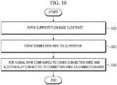
- Yet another aspect of the present invention provides a method of manufacturing a display device, the method including forming a supporter on a base substrate, forming a connection wire on the supporter, and forming a signal wire, which covers the connection wire and is electrically connected to the connection wire, on the connection wire, wherein the connection wire may cover the supporter and may be in direct contact with the supporter.
- the forming of the supporter on the base substrate may further include forming the supporter through a photolithography process, an inkjet process, or a squeezing process.
- the method may further include, after forming the signal wire, attaching a driving integrated circuit onto the signal wire.
- the attaching of the driving integrated circuit may include directly connecting the bump to the signal wire.
- the signal wire may include a first portion disposed to overlap the supporter, a second portion disposed not to overlap the supporter and located on one side of the first portion, and a third portion disposed not to overlap the supporter and located on the other side of the first portion, wherein an upper surface of the first portion may protrude further than an upper surface of the second portion and an upper surface of the third portion in a thickness direction.
- the bump may include a first portion, a second portion disposed on one side of the first portion, and a third portion disposed on the other side of the first portion, wherein a surface of the first portion may be indented further than a surface of the second portion and a surface of the third portion in the thickness direction.
- the first portion of the signal wire may be connected to the first portion of the bump
- the second portion of the signal wire may be connected to the second portion of the bump
- the third portion of the signal wire may be connected to the third portion of the bump.
- a display device having high bonding reliability can be provided.
- Display devices are devices for displaying a video or a still image.
- the display devices may be used for implementing display screens of various kinds of products such as televisions, notebook computers, monitors, digital signage, and Internet of Things (IoT) devices, as well as portable electronic devices such as mobile phones, smartphones, tablet personal computers (PCs), smart watches, watch phones, mobile communication terminals, electronic organizers, electronic books, portable multimedia players (PMPs), navigation devices, and ultra-mobile PCs (UMPCs).
- IoT Internet of Things
- portable electronic devices such as mobile phones, smartphones, tablet personal computers (PCs), smart watches, watch phones, mobile communication terminals, electronic organizers, electronic books, portable multimedia players (PMPs), navigation devices, and ultra-mobile PCs (UMPCs).
- PCs personal computers
- PMPs portable multimedia players
- UMPCs ultra-mobile PCs
- FIG. 1 is a plan layout view of a display device according to one embodiment
- FIG. 2 is a schematic partial cross-sectional view of the display device according to one embodiment.
- a display device 1 includes a display area DA that displays an image and a non-display area NDA disposed around the display area DA.
- the display area DA may have a rectangular shape in which each corner has a right angle in a plan view or a rectangular shape in which each corner is round in a plan view.
- a planar shape of the display area DA is not limited to the rectangular shape and may be a circular shape, an elliptical shape, or various other shapes.
- the display area DA includes a plurality of pixels. A detailed cross-sectional structure of the pixel will be described below.
- the non-display area NDA is disposed around the display area DA.
- the non-display area NDA may be disposed adjacent to both short sides of the display area DA.
- the non-display area NDA may be disposed adjacent to both long sides of the display area DA in addition to both short sides thereof and may surround all of the sides of the display area DA. That is, the non-display area NDA may form edges of the display area DA.
- the display device 1 may include a display panel 100, which displays a screen, and a driving integrated circuit 300 that is attached to the display panel 100 and drives a pixel circuit of the display panel 100.
- the driving integrated circuit 300 may be implemented as a chip on plastic (COP) in which a driving chip (IC) is applied and which is mounted directly on the display panel 100.
- COP chip on plastic
- an organic light-emitting display panel may be applied.
- the display panel 100 to which an organic light-emitting display panel is applied is exemplified in the following embodiment, the present invention is not limited thereto, and other types of display panels such as a liquid crystal display (LCD) panel, a field emission display (FED) panel, an electrophoretic apparatus, and the like may be applied thereto.
- LCD liquid crystal display
- FED field emission display
- electrophoretic apparatus an electrophoretic apparatus, and the like
- the display panel 100 may include a main area MA and a bending area BA.
- the main area MA may be flat.
- the display area DA and a partial area of the non-display area NDA of the display panel 100 may be disposed.
- the bending area BA may be disposed on at least one side of the main area MA.
- one bending area BA is exemplified as being disposed adjacent to a lower side of the main area MA.
- the bending area BA may be disposed adjacent to other sides such as left, right, and upper sides of the main area MA.
- the bending area BA may be disposed on two or more sides of the main area MA.
- the bending area BA may be bent in a direction opposite to a display direction (a back surface in the case of a top emission type device). As described above, when at least a portion of the non-display area NDA is bent in the direction opposite to the display direction, a bezel of the display device may be reduced.
- the display device 1 may further include a sub area SA extending from the bending area BA.
- the sub area SA may be parallel to the main area MA.
- the sub area SA may overlap the main area MA in a thickness direction.
- the above-described bending area BA and sub area SA may each be the non-display area NDA, but the present invention is not limited thereto.
- the display panel 100 may include a pad area PA disposed in the non-display area NDA.
- the pad area PA may be located in the sub area SA as exemplified in the drawing. However, the pad area PA is not limited thereto and may be located in the main area MA or the bending area BA.
- the driving integrated circuit 300 may be attached to the pad area PA of the display panel 100.
- a plurality of signal wires are disposed in the pad area PA of the non-display area NDA.
- the plurality of signal wires may be connected to at least one thin-film transistor of the pixel in the display area DA through a connection wire electrically connected to the thin-film transistor.
- the connection wire may be disposed across the display area DA and the non-display area NDA.
- Bumps of the driving integrated circuit 300 may be connected to the plurality of signal wires.
- the display device may further include a printed circuit board 500 attached to the display panel 100.
- the printed circuit board 500 may be attached to the outside of the pad area PA of the display panel 100 in the non-display area NDA. That is, the pad area PA to which the driving integrated circuit 300 is attached may be disposed between the display area DA and an area to which the printed circuit board 500 are attached.
- the printed circuit board 500 may be attached to an end portion of a lower surface of the sub area SA.
- the printed circuit board 500 may be a flexible printed circuit board (FPCB).
- FPCB flexible printed circuit board
- the printed circuit board 500 is not limited thereto and may be connected to the display panel 100 through a flexible film.
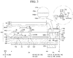
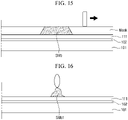
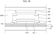
- FIG. 3 is a cross-sectional view of one pixel and the pad area according to one embodiment.
- the display device 1 further includes a panel bottom sheet 200 disposed below the display panel 100.
- the panel bottom sheet 200 may be attached to a back surface of the display panel 100.
- the panel bottom sheet 200 includes at least one functional layer.
- the functional layer may be a layer that performs a heat dissipation function, an electromagnetic wave shielding function, a grounding function, a buffering function, a strength reinforcing function, a supporting function, and/or a digitizing function.
- the functional layer may be a sheet layer formed of a sheet, a film layer formed of a film, a thin film layer, a coating layer, a panel, a plate, or the like.
- One functional layer may be formed of a single layer or formed of a plurality of stacked thin films or coating layers.
- the functional layer may be, for example, a support substrate, a heat dissipation layer, an electromagnetic wave shielding layer, a shock-absorbing layer, a digitizer, or the like.
- the display panel 100 may include a display substrate 101, a plurality of conductive layers, a plurality of insulating layers insulating the plurality of conductive layers, an organic layer EL, and the like.
- the display substrate 101 is disposed across the entirety of the display area DA and the non-display area NDA.
- the display substrate 101 may perform a function of supporting various elements disposed thereabove.
- the display substrate 101 may be a rigid substrate including a rigid material such as flexible glass, quartz, or the like.
- the display substrate 101 is not limited thereto and may be a flexible substrate including a flexible material such as polyimide (PI) or the like.
- a buffer layer 102 may be disposed on the display substrate 101.
- the buffer layer 102 may prevent moisture and oxygen from penetrating from the outside through the display substrate 101.
- the buffer layer 102 may include one of a silicon nitride (SiN x ) film, a silicon oxide (SiO 2 ) film, and a silicon oxynitride (SiO x N y ) film.
- a semiconductor layer 105 may be disposed on the buffer layer 102.
- the semiconductor layer 105 forms a channel of a thin-film transistor.
- the semiconductor layer 105 may be disposed in each pixel of the display area DA and may be disposed even in the non-display area NDA in some cases.
- the semiconductor layer 105 may include a source/drain area and an active area.
- the semiconductor layer 105 may include polycrystalline silicon.
- a first insulating layer 111 may be disposed on the semiconductor layer 105.
- the first insulating layer 111 may be disposed over the entire surface of the display substrate 101.
- the first insulating layer 111 may be a gate insulating film having a gate insulating function.
- the first insulating layer 111 may include a silicon compound, a metal oxide, or the like.
- the first insulating layer 111 may include silicon oxide, silicon nitride, silicon oxynitride, aluminum oxide, tantalum oxide, hafnium oxide, zirconium oxide, titanium oxide, or the like. The above materials may be used alone or in combination thereof.
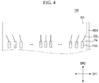
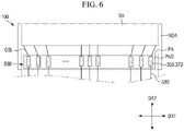
- a supporter SM may be disposed on the first insulating layer 111.
- the supporter SM may be disposed directly on an upper surface of the first insulating layer 111.
- the supporter SM may be disposed below a connection wire GSL, which will be described below, to protrude the connection wire GSL in the thickness direction. Due to the protruding connection wire GSL, a signal wire PAD may protrude together with the connection wire GSL in the thickness direction to facilitate bonding with the bumps of the driving integrated circuit 300.
- the supporter SM may include an organic material or an inorganic material.
- a cross-sectional shape of the supporter SM may be a trapezoidal shape.
- a first conductive layer 120 may be disposed on the first insulating layer 111 and the supporter SM.
- the first conductive layer 120 may include a gate electrode GE of a thin-film transistor TFT, a first electrode CE1 of a storage capacitor Cst, and the connection wire GSL.
- the connection wire GSL may be disposed to pass through the display area DA and the pad area PA.
- the first conductive layer 120 may include one or more metals selected from among molybdenum (Mo), aluminum (Al), platinum (Pt), palladium (Pd), silver (Ag), magnesium (Mg), gold (Au), nickel (Ni), neodymium (Nd), iridium (Ir), chromium (Cr), calcium (Ca), titanium (Ti), tantalum (Ta), tungsten (W), and copper (Cu).
- the first conductive layer 120 may be a single film or a stacked film made of the above-exemplified materials.
- connection wire GSL may cover a surface of the supporter SM and may be in direct contact with the surface of the supporter SM. A portion of the connection wire GSL overlapping the supporter SM in the thickness direction may protrude in the thickness direction.
- Second insulating layers 112a and 112b may be disposed on the first conductive layer 120.
- the second insulating layers 112a and 112b may insulate the first conductive layer 120 and a second conductive layer 130 from each other.
- the second insulating layer 112a may be disposed mainly in the display area DA, and the second insulating layer 112b may be disposed mainly in the pad area PA.
- the second insulating layers 112a and 112b may be made of a material selected from the exemplified materials of the first insulating layer 111.
- the second insulating layer 112b may partially expose the connection wire GSL in the pad area PA.
- the second insulating layer 112b may partially cover a side surface of the connection wire GSL and expose an upper surface and a portion of the remaining side surface thereof.
- the second conductive layer 130 may be disposed on the second insulating layers 112a and 112b.
- the second conductive layer 130 may include a second electrode CE2 of the storage capacitor Cst.
- a material of the second conductive layer 130 may be selected from the above-exemplified materials of the first conductive layer 120.
- the first electrode CE1 of the storage capacitor Cst and the second electrode CE2 of the storage capacitor Cst may form a capacitor through the second insulating layers 112a and 112b.
- a third insulating layer 113 may be disposed on the second conductive layer 130.
- the third insulating layer 113 may include at least one of the above-exemplified materials of the first insulating layer 111.
- the third insulating layer 113 may include an organic insulating material.
- the organic insulating material may be selected from exemplified materials of a first via layer VIA1, which will be described below.
- a third conductive layer 140 may be disposed on the third insulating layer 113, the second insulating layer 112b, and the connection wire GSL.
- the third conductive layer 140 may include a source electrode SE, a drain electrode DE, a high-potential voltage electrode ELVDDE, and the signal wire PAD
- the third conductive layer 140 may include at least one selected from among molybdenum (Mo), aluminum (Al), platinum (Pt), palladium (Pd), silver (Ag), magnesium (Mg), gold (Au), nickel (Ni), neodymium (Nd), iridium (Ir), chromium (Cr), calcium (Ca), titanium (Ti), tantalum (Ta), tungsten (W), and copper (Cu).
- the third conductive layer 140 may be a single film made of a material selected from the above-exemplified materials.
- the third conductive layer 140 is not limited thereto and may be a stacked film.
- the third conductive layer 140 may be formed in a stacked structure of Ti/Al/Ti, Mo/Al/Mo, Mo/AlGe/Mo, Ti/Cu, or the like.
- the third conductive layer 140 may be formed in a stacked structure of Ti/Al/Ti.
- the signal wire PAD of the third conductive layer 140 may be disposed to overlap the connection wire GSL of the first conductive layer 120 in the thickness direction and may be electrically connected to the connection wire GSL through the exposed portion of the second insulating layer 112b.
- a planar size of the signal wire PAD may be greater than a planar size of the connection wire GSL.
- the signal wire PAD may cover the connection wire GSL in a plan view, and include a side surface extending further outward than the side surface of the connection wire GSL.
- the first via layer VIA1 may be disposed on the third conductive layer 140.
- the first via layer VIA1 may include an organic insulating material.
- the organic insulating material may include at least one among an acrylic-based resin (polyacrylate resin), an epoxy resin, a phenolic resin, a polyamide-based resin, a polyimide-based resin, an unsaturated polyester-based resin, a polyphenylene-based resin (polyphenylene ether resin), a polyphenylene sulfide-based resin, and benzocyclobutene (BCB).
- the third insulating layer 113 and upper structures of the third conductive layer 140 may be removed or omitted in a partial area of the signal wire PAD on the pad area PA. Accordingly, the omitted or removed structures may expose the signal wire PAD disposed in the pad area PA.
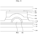
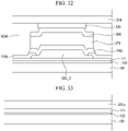
- the driving integrated circuit 300 may include a driving substrate 310, a driving wire 330 disposed on the driving substrate 310, and a bump disposed on the driving wire 330.
- the bump may include a first bump 350 disposed on a surface of the driving wire 330, and a second bump 370 disposed on a surface of the first bump 350.
- the driving substrate 310 may include at least one of the exemplified materials of the display substrate 101.
- the driving substrate 310 may serve to support lower structures of the driving integrated circuit 300.
- the driving wire 330 may include at least one selected from among molybdenum (Mo), aluminum (Al), platinum (Pt), palladium (Pd), silver (Ag), magnesium (Mg), gold (Au), nickel (Ni), neodymium (Nd), iridium (Ir), chromium (Cr), calcium (Ca), titanium (Ti), tantalum (Ta), tungsten (W), and copper (Cu).
- the driving wire 330 may be a single film made of a material selected from the above-exemplified materials.
- the driving wire 330 is not limited thereto and may be a stacked film.
- the bump may be bonded to the signal wire PAD of the display panel 100.
- the first bump 350 may include at least one selected from among molybdenum (Mo), aluminum (Al), platinum (Pt), palladium (Pd), silver (Ag), magnesium (Mg), gold (Au), nickel (Ni), neodymium (Nd), iridium (Ir), chromium (Cr), calcium (Ca), titanium (Ti), tantalum (Ta), tungsten (W), and copper (Cu).
- the first bump 350 may be a single film made of a material selected from the above-exemplified materials.
- the first bump 350 is not limited thereto and may be a stacked film.
- the second bump 370 may include at least one selected from among molybdenum (Mo), aluminum (Al), platinum (Pt), palladium (Pd), silver (Ag), magnesium (Mg), gold (Au), nickel (Ni), neodymium (Nd), iridium (Ir), chromium (Cr), calcium (Ca), titanium (Ti), tantalum (Ta), tungsten (W), and copper (Cu).
- the second bump 370 may be a single film made of a material selected from the above-exemplified materials.
- the second bump 370 is not limited thereto and may be a stacked film.
- a non-conductive member NCM may be disposed on the periphery of the signal wire PAD and the bump.
- the non-conductive member NCM may be disposed between adjacent signal wires PAD and between adjacent bumps.
- the non-conductive member NCM may be disposed between the driving substrate 310 and the second insulating layer 112b.
- the non-conductive member NCM may be disposed between adjacent signal wires PAD, between adjacent bumps, and between the signal wire PAD and the bump before an ultrasonic bonding process, which will be described below, is performed, and during the ultrasonic bonding process, the non-conductive members NCM located between the signal wire PAD and the bump may be pushed out into an area not overlapping the signal wire PAD and the bump to fill a gap between the adjacent signal wires PAD and a gap between the adjacent bumps together with the non-conductive members NCM located between the adjacent signal wires PAD and between the adjacent bumps.
- the non-conductive member NCM may be made of a material having no conductivity or substantially no conductivity.
- the non-conductive member NCM may include a non-conductive film (NCF) or a non-conductive paste (NCP).
- the bump may be directly connected to the exposed signal wire PAD.
- the bump may be ultrasonically bonded to the signal wire PAD.
- the second bump 370 may be directly connected to the signal wire PAD and may be ultrasonically bonded thereto.
- the ultrasonic bonding may be performed through an ultrasonic device 700.
- the ultrasonic device 700 may include a vibration generation part 710, a vibration part 720 connected to the vibration generation part 710, a pressing part 730 configured to amplify a vibration amplitude of the vibration part 720, and a vibration transmitting part 740 connected to the vibration part 720.
- the vibration generation part 710 may convert electrical energy into vibration energy.
- the vibration part 720 may vibrate by the vibration energy converted by the vibration generation part 710.
- the vibration part 720 may vibrate while having a constant vibration direction and a predetermined amplitude.
- the amplitude of the vibration part 720 may be amplified in a direction parallel to the vibration direction by the pressing part 730 connected to the vibration part 720.
- the vibration transmitting part 740 may transmit the vibration of the vibration part 720 to an ultrasonic bonding object.
- a support part 750 may fix upper and lower surfaces of the vibration part 720 to suppress the vibration part 720 and the vibration transmitting part 740 from moving up and down due to the vibration.
- the ultrasonic device 700 is in contact with the other surface of the driving integrated circuit 300 and maintains a constant pressurized state downward so that the vibration transmitting part 740 efficiently transmits the vibration to the driving integrated circuit 300.
- the vibration transmitting part 740 of the ultrasonic device 700 may perform the ultrasonic bonding while overlapping the entire area of the driving integrated circuit 300 disposed therebelow.
- the ultrasonic device 700 may vibrate the bump in a vibration direction while vibrating in the predetermined vibration direction.
- the signal wire PAD may vibrate slightly in the vibration direction due to the vibration transmitted through the bump, a vibration amplitude thereof may be insignificant.
- the vibration amplitude of the vibration transmitting part 740 in the vibration direction may be regarded as substantially the same as a distance that the bump moves on the signal wire PAD in the vibration direction.
- the vibration direction may be a second direction DR2. That is, the vibration direction may be a direction in which the signal wire PAD and a long side of the bump extend.
- the bump When the bump is ultrasonically vibrated on one surface of the signal wire PAD, a predetermined frictional force is generated at an interface between one surface of the signal wire PAD and one surface of the bump, and frictional heat may be generated due to the frictional force.
- a pad melting area PADb adjacent to the bump of the signal wire PAD and a bump melting area 370b adjacent to the signal wire PAD of the bump may be melted.
- the signal wire PAD may include a pad non-melting area PADa and the pad melting area PADb.
- the bump may include a bump non-melting area 370a and the bump melting area 370b.
- the pad non-melting area PADa may be an area including only the material included in the signal wire PAD.
- the bump non-melting area 370a may be an area including only the material included in the bump.
- the pad melting area PADb may be an area in which the material included in the bump is diffused, and the material of the signal wire PAD and the material of the bump are mixed, and the bump melting area 370b may be an area in which the material in the signal wire PAD is diffused, and the material of the bump and the material of the signal wire PAD are mixed.
- the signal wire PAD and the bump may be bonded to each other through solidification.
- An interface between the signal wire PAD and the bump i.e., an interface between the pad melting area PADb and the bump melting area 370b, may have a non-flat shape.
- the vibration transmitting part 740 of the ultrasonic device 700 presses an upper surface of the printed base film 310 of the driving integrated circuit 300 in a third direction DR3 and applies the vibration along the second direction DR2, and accordingly, the bump disposed on the printed base film 310 is bonded to the signal wire PAD as described above.
- the vibration transmitting part 740 of the ultrasonic device 700 may be separated from the printed base film 310 in the thickness direction DR3, and a bonding force between the signal wire PAD and the bump may be greater than a bonding force between the bump and the printed base film 310, and thus delamination may occur between the bump and the printed base film 310.
- the display device 1 may prevent the delamination between the bump and the printed base film 310 in advance by arranging a first curable pattern IRP between adjacent bumps as will be described below.
- a fourth conductive layer 150 may be disposed on the first via layer VIA1.
- the fourth conductive layer 150 may include a data line DL, a connection electrode CNE, and a high-potential voltage wire ELVDDL.
- the data line DL may be electrically connected to the source electrode SE of the thin-film transistor TFT through a contact hole passing through the first via layer VIA1.
- the connection electrode CNE may be electrically connected to the drain electrode DE of the thin-film transistor TFT through a contact hole passing through the first via layer VIA1.
- the high-potential voltage wire ELVDDL may be electrically connected to the high-potential voltage electrode ELVDDE through a contact hole passing through the first via layer VIA1.
- the fourth conductive layer 150 may include a material selected from the exemplified materials of the third conductive layer 140.
- a second via layer VIA2 is disposed on the fourth conductive layer 150.
- the second via layer VIA2 may include at least one of the above-exemplified materials of the first via layer VIA1.
- An anode AND is disposed on the second via layer VIA2.
- the anode AND may be electrically connected to the connection electrode CNE through a contact hole passing through the second via layer VIA2.
- a bank layer BANK may be disposed on the anode AND
- the bank layer BANK may include a contact hole that exposes the anode AND
- the bank layer BANK may be made of an organic insulating material or an inorganic insulating material.
- the bank layer BANK may include at least one of a photoresist, a polyimide-based resin, an acrylic-based resin, a silicon compound, a polyacrylic-based resin, and the like.
- the organic layer EL may be disposed on an upper surface of the anode AND in an opening of the bank layer BANK
- a cathode CAT is disposed on the organic layer EL and the bank layer BANK
- the cathode CAT may be a common electrode disposed across a plurality of pixels.
- a thin-film encapsulation layer 170 is disposed on the cathode CAT.
- the thin-film encapsulation layer 170 may cover an organic light-emitting diode (OLED).
- the thin-film encapsulation layer 170 may be a stacked film in which inorganic films and organic films are alternately stacked.
- the thin-film encapsulation layer 170 may include a first encapsulation inorganic film 171, an encapsulation organic film 172, and a second encapsulation inorganic film 173, which are sequentially stacked.
- FIG. 4 is a plan layout view of the pad area of the display panel according to one embodiment
- FIG. 5 is a plan layout view of the driving integrated circuit according to one embodiment
- FIG. 6 is a plan layout view of the pad area of the display panel to which the driving integrated circuit is attached
- FIG. 7 is a partial enlarged view of FIG. 6
- FIG. 8 is a cross-sectional view taken along line VIII-VIII' of FIG. 7
- FIG. 9 is a cross-sectional view taken along line IX-IX' of FIG. 7 .
- a plurality of signal wires PAD may be provided, and the plurality of signal wires PAD may be arranged along a first direction DR1.
- the plurality of signal wires PAD may include a power pad, a data pad, and a panel dummy pad.
- the bumps 350 and 370 of the driving integrated circuit 300 may include a plurality of bumps, and the plurality of bumps may be arranged along the first direction DR1.
- a planar shape of each of the signal wire PAD and the bumps 350 and 370 may be a rectangular shape. That is, each of the signal wire PAD and the bumps 350 and 370 may include long sides extending along the second direction DR2 and short sides extending along the first direction DR1. A corner at which the long side and the short side meet may form a right angle.
- the planar shape of each of the signal wire PAD and the bumps 350 and 370 is not limited thereto, and of course, a square shape, a circular shape, an elliptical shape, other polygonal shape, or the like may be applied.
- planar size of the signal wire PAD and a planar size of each of the bumps 350 and 370 may be substantially the same, but are not limited thereto, and the planar size of the signal wire PAD may be greater than the planar size of each of the bumps 350 and 370, and vice versa.
- connection wire GSL may be disposed to cross from the display area DA to the pad area PA, and may have a shape in which a width is increased in the first direction DR1 in an area overlapping the signal wire PAD of the pad area PA.
- the planar size of the signal wire PAD may be greater than the planar size of each of the connection wire GSL and the supporter SM.
- the signal wire PAD may be disposed to overlap the connection wire GSL and the supporter SM in the thickness direction.
- the planar size of the supporter SM may be less than the planar size of the connection wire GSL.
- a planar shape of the supporter SM may be a rectangular shape, but is not limited thereto, and a square shape, a circular shape, an elliptical shape, other polygonal shape, or the like may be applied.
- the driving wire 330 may be disposed to extend from an end portion of a lower side of the display panel 100 in the second direction DR2 in a plan view to the pad area PA.
- the driving wire 330 may have a shape in which a width extends in the first direction DR1 in an area overlapping the signal wire PAD and the bumps 350 and 370 in the thickness direction.
- a planar shape of the driving wire 330 may be a rectangular shape in an area overlapping the signal wire PAD and the bumps 350 and 370 in the thickness direction. That is, in the above-described area, the driving wire 330 may include short sides extending along the first direction DR1 and long sides extending along the second direction DR2, and a corner at which the long side and the short side meet may form a right angle.
- the planar shape of the driving wire 330 is not limited thereto, and of course, a square shape, a circular shape, an elliptical shape, other polygonal shape, or the like may be applied.
- a planar size of the driving wire 330 may be substantially the same as the planar size of the connection wire GSL described above. However, the planar size of the driving wire 330 is not limited thereto, and may be less or greater than the planar size of the connection wire GSL.
- the bumps 350 and 370 may be disposed to overlap the signal wire PAD and the driving wire 330 in the thickness direction.
- the planar size of each of the bumps 350 and 370 may be substantially the same as the planar size of the signal wire PAD.
- the planar size of each of the bumps 350 and 370 may be greater than the planar size of the driving wire 330.
- the supporter SM may be covered by the connection wire GSL disposed thereabove. As shown in FIG. 9 , when the supporter SM is applied in a trapezoidal shape, the supporter SM may include an upper surface, a lower surface, and side surfaces. The connection wire GSL may be disposed on the upper and side surfaces of the supporter SM.
- the lower surface of the supporter SM may be in direct contact with the first insulating layer 111.
- the upper and side surfaces of the supporter SM may be covered by and in direct contact with the connection wire GSL.
- the connection wire GSL may be formed along the surface of the supporter SM along the shape of the supporter SM.
- An overall thickness of the connection wire GSL may be the same. That is, the thickness of a portion of the connection wire GSL disposed on the upper surface of the supporter SM and the thickness of a portion of the connection wire GSL disposed on the side surface of the supporter SM may be substantially the same.
- a surface of the connection wire GSL may include an inner surface and an outer surface.
- the outer surface of the connection wire GSL may include an upper surface GSLa1 and outer side surfaces GSLa2 and GSLa3, and the inner surface of the connection wire GSL may include a lower surface GSLb1 and inner side surfaces GSLb2 and GSLb3.
- the lower surface GSLb1 of the connection wire GSL may be in direct contact with the upper surface of the supporter SM.
- the inner side surfaces GSLb2 and GSLb3 of the connection wire GSL may be in direct contact with the side surfaces of the supporter SM, respectively.
- the second insulating layer 112b may be further disposed on the side surface of the connection wire GSL.
- the second insulating layer 112b may be in direct contact with the supporter SM and the upper surface of the first insulating layer 111 exposed by the connection wire GSL.
- the second insulating layer 112b may be disposed on the outer side surfaces GSLa2 and GSLa3 of the connection wire GSL.
- the second insulating layer 112b may expose an upper end portion of each of the outer side surfaces GSLa2 and GSLa3 of the connection wire GSL and cover a lower end portion of each of the outer side surfaces GSLa2 and GSLa3.
- the second insulating layer 112b may be in direct contact with the lower end portion of each of the outer side surfaces GSLa2 and GSLa3 of the connection wire GSL.
- the signal wire PAD may be disposed on the second insulating layer 112b and the connection wire GSL.
- the signal wire PAD may be disposed on the upper surface and the side surfaces of the connection wire GSL.
- An overall thickness of the signal wire PAD may be the same. That is, the thickness of a portion of the signal wire PAD disposed on the upper surface of the connection wire GSL and the thickness of a portion of the signal wire PAD disposed on the side surfaces of the connection wire GSL may be substantially the same.
- a surface of the signal wire PAD may include an inner surface and an outer surface.
- the inner surface of the signal wire PAD may include a first upper surface PADa1, a second upper surface PADa3, and an outer side surface PADa2 disposed between the first upper surface PADa1 and the second upper surface PADa3 and connecting the first upper surface PADa1 and the second upper surface PADa3, and the outer surface of the signal wire PAD may include a first lower surface PADb1, a second lower surface PADb3, and an inner side surface PADb2 disposed between the first lower surface PADb1 and the second lower surface PADb3 and connecting the first lower surface PADb1 and the second lower surface PADb3.
- the second upper surface PADa3 and the outer side surface PADa2 may be further located in opposite directions symmetrically with respect to the first upper surface PADa1.
- the second lower surface PADb3 and the inner side surface PADb2 may be further located in opposite directions symmetrically with respect to the first lower surface PADb1.
- the first lower surface PADb1 of the signal wire PAD may be located to protrude further upward than the second lower surface PADb3 in the thickness direction.
- the first upper surface PADa1 of the signal wire PAD may be located to protrude further upward than the second upper surface PADa3 in the thickness direction.
- the first lower surface PADb1 of the signal wire PAD may be in direct contact with the upper surface PADb1 of the connection wire GSL
- the inner side surface PADb2 of the signal wire PAD may be in direct contact with the upper end portion of the outer side surface GSLa2 of the connection wire GSL exposed by the second insulating layer 112b
- the second lower surface PADb3 of the signal wire PAD may be in direct contact with the upper surface of the second insulating layer 112b.
- the first upper surface PADa1, the second upper surface PADa3, and the outer side surface PADa2 of the signal wire PAD may be in contact with the bump.
- a surface of the second bump 370 may include an outer surface facing the signal wire PAD.
- the outer surface of the second bump 370 may include a first lower surface 370a1, a second lower surface 370a3, and an outer side surface 370a2 disposed between the first lower surface 370a1 and the second lower surface 370a3 and physically connecting the first lower surface 370a1 and the second lower surface 370a3.
- the second lower surface 370a3 and the outer side surface 370a2 may be further located in opposite directions symmetrically with respect to the first lower surface 370a1.
- the first lower surface 370a1 of the second bump 370 may be located to be indented further upward than the second lower surface 370a3 in the thickness direction.
- the first lower surface 370a1 of the second bump 370 may be in direct contact with the first upper surface PADa1 of the signal wire PAD, and the second lower surface 370a3 of the second bump 370 may be in direct contact with the second upper surface PADa3 of the signal wire PAD, and the outer side surface 370a2 of the second bump 370 may be in direct contact with the outer side surface PADa2 of the signal wire PAD.
- the first lower surface 370a1, the second lower surface 370a3, and the outer side surface 370a2 may be in direct contact with the first upper surface PADa1, the second upper surface PADa3, and the outer side surface PADa2, respectively.
- the first lower surface 370a1, the second lower surface 370a3, and the outer side surface 370a2 may be ultrasonically connected or ultrasonically bonded to the first upper surface PADa1, the second upper surface PADa3, and the outer side surface PADa2, respectively.
- the surface of the signal wire PAD may be in contact with the connection wire GSL therebelow and the second insulating layer 112b, and the supporter SM may be disposed between first insulating layer 111 and the connection wire GSL so that the surface of a central portion of the connection wire GSL may protrude in the thickness direction, and the surface of a central portion of the signal wire PAD disposed along the surface of the connection wire GSL may protrude in the thickness direction.
- the signal wire PAD having a shape in which the surface of the central portion protrudes in the thickness direction may be engaged with the shape of the second bump 370 of the driving integrated circuit 300.
- the signal wire PAD may include a first portion (the central portion) having a first surface height and second portions (edge portions) disposed on one side and the other side of the first portion in the first direction DR1 and having a second surface height less than the first surface height
- the second bump 370 may include a first portion (the central portion) having a third surface height and second portions (edge portions) disposed on one side and the other side of the first portion in the first direction DR1 and having a fourth surface height greater than the third surface height.
- the protruding first portion of the signal wire PAD may be coupled to the indented first portion of the second bump 370
- the indented second portion of the signal wire PAD may be coupled to the protruding second portion of the second bump 370. Accordingly, bonding reliability and a contact area between the signal wire PAD and the second bump 370 may be increased, and resistance between the second bump 370 and the signal wire PAD may be reduced.
- FIG. 10 is a flowchart of a method of manufacturing the display device according to one embodiment
- FIGS. 11 and 12 are cross-sectional views illustrating a processing operation of the method of manufacturing the display device according to one embodiment
- FIG. 13 is a cross-sectional view illustrating a processing operation of a method of manufacturing the display device according to another embodiment
- FIGS. 14 and 15 are cross-sectional views illustrating a processing operation of a method of manufacturing the display device according to still another embodiment
- FIGS. 16 and 17 are cross-sectional views illustrating a processing operation of a method of manufacturing the display device according to yet another embodiment
- FIG. 18 is a cross-sectional view illustrating the processing operation of the method of manufacturing the display device according to one embodiment.
- a supporter is formed on a display substrate 101 or a base substrate (S10).
- a supporter SM may be disposed on a first insulating layer 111.
- the supporter SM may be directly disposed on an upper surface of the first insulating layer 111.
- the supporter SM may be disposed below the above-described connection wire GSL to protrude the connection wire GSL in the thickness direction. Due to the protruding connection wire GSL, a signal wire PAD may protrude together with the connection wire GSL in the thickness direction to facilitate bonding with bumps of a driving integrated circuit 300.
- the supporter SM may include an organic material or an inorganic material.
- a cross-sectional shape of the supporter SM may be a trapezoidal shape.
- FIGS. 12 to 17 illustrate various methods of forming the supporter SM.
- the operation of forming the supporter on the display substrate 101 or the base substrate (S10) may further include an operation of forming the supporter SM through a photolithography process.
- the operation of forming the supporter SM through the photolithography process may further include operations of applying a supporter material SMa on the first insulating layer 111, irradiating the supporter material SMa applied on the first insulating layer 111 with an ultraviolet (UV) laser, and developing the supporter material SMa irradiated with the ultraviolet laser to form the supporter SM.
- the operation of irradiating the supporter material SMa applied on the first insulating layer 111 with the ultraviolet (UV) laser may further include operations of disposing a mask MASK illustrated in FIG. 13 in an area except for the area where the supporter SM is formed, and irradiating the supporter material with the ultraviolet laser.
- the operation of forming the supporter on the display substrate 101 or the base substrate (S10) may further include an operation of forming a supporter SM through a squeezing process.
- the operation of forming the supporter SM through the squeezing process may further include operations of disposing a masking pattern MK on a first insulating layer 111 in an area except for a supporter disposing area, filling a supporter material SMb on the first insulating layer 111 exposed by the masking pattern MK by pushing the supporter material SMb through a squeezing device, and removing the masking pattern MK from the first insulating layer 111 and curing the supporter material SMb formed on an upper surface of the first insulating layer 111.
- the operation of forming the supporter on the display substrate 101 or the base substrate (S10) may further include an operation of forming a supporter SM through an inkjet process.
- the operation of forming the supporter SM through the inkjet process may include operations of applying a supporter material SMc1 onto a first insulating layer 111 through an inkjet device, and curing the supporter material SMc1 applied onto the first insulating layer 111 to form the supporter SM.
- connection wire GSL is formed on the supporter SM (S20).
- the connection wire GSL may include one or more metals selected from among molybdenum (Mo), aluminum (Al), platinum (Pt), palladium (Pd), silver (Ag), magnesium (Mg), gold (Au), nickel (Ni), neodymium (Nd), iridium (Ir), chromium (Cr), calcium (Ca), titanium (Ti), tantalum (Ta), tungsten (W), and copper (Cu).
- the connection wire GSL may be a single film or a stacked film made of the above-exemplified materials.
- connection wire GSL may be formed to cover a surface of the supporter SM and to be in direct contact with the surface of the supporter SM. A portion of the connection wire GSL overlapping the supporter SM in the thickness direction may protrude in the thickness direction.
- FIG. 19 is a cross-sectional view of a pad area of a display device according to another embodiment
- FIG. 20 is a cross-sectional view of a pad area of a display device according to still another embodiment
- FIG. 21 is a cross-sectional view of a pad area of a display device according to yet another embodiment
- FIG. 22 is a cross-sectional view of a pad area of a display device according to yet another embodiment
- FIG. 23 is a cross-sectional view of a pad area of a display device according to yet another embodiment.
- FIGS. 19 to 23 illustrate various cross-sectional shapes of the supporter SM.
- a cross-sectional shape of a supporter SM_1 may be applied in a triangular shape.
- a cross-sectional shape of a supporter SM_2 may be applied in a pentagonal shape.
- a cross-sectional shape of a supporter SM_3 may be applied in a semicircular shape.
- a cross-sectional shape of a supporter SM_4 may be applied in a semi-elliptical shape.
- a cross-sectional shape of a supporter SM_5 may be applied in a quadrangular shape.
- FIG. 24 is a plan layout view of a pad area of a display panel to which a driving integrated circuit according to another embodiment is attached.
- a supporter SM_6 is different from the supporter SM of FIG. 7 in that the supporter SM_6 may have a line shape extending along a long-side direction of a signal wire PAD, and the supporter SM_6 having a line shape may include a plurality of patterns.
- the supporter SM_6 may have a line shape extending along the long-side direction or a column direction of the signal wire PAD, and the supporter SM_6 having a line shape may include the plurality of patterns.
- the plurality of line-shaped patterns may be disposed to be spaced apart from each other along a short-side direction of the signal wire PAD.
- the number of line-shaped patterns is three, but is not limited thereto, and may be two or four or more.
- FIG. 25 is a plan layout view of a pad area of a display panel to which a driving integrated circuit according to still another embodiment is attached.
- a supporter SM_7 is different from the supporter SM of FIG. 7 in that the supporter SM_7 may have a line shape extending along a short-side direction or a row direction of a signal wire PAD, and the supporter SM_7 having a line shape may include a plurality of patterns.
- the supporter SM_7 may have a line shape extending along the short-side direction of the signal wire PAD, and the supporter SM_7 having a line shape may include the plurality of patterns.
- the plurality of line-shaped patterns may be disposed to be spaced apart from each other along a long-side direction of the signal wire PAD.
- the number of line-shaped patterns is six, but is not limited thereto, and may be two, three, four, five, or seven or more.
- FIG. 26 is a plan layout view of a pad area of a display panel to which a driving integrated circuit according to yet another embodiment is attached.
- a supporter SM_8 according to the present embodiment is different from the supporter SM of FIG. 7 in that the supporter SM_8 has a lattice shape extending along a long-side direction and a short-side direction of a signal wire PAD.
- the supporter SM_8 may have a lattice shape extending along the long-side direction and the short-side direction of the signal wire PAD.
- FIG. 27 is a plan layout view of a pad area of a display panel to which a driving integrated circuit according to yet another embodiment is attached.
- a supporter SM_9 according to the present embodiment is different from the supporter SM of FIG. 7 in that the supporter SM_9 includes a plurality of patterns having an island shape.
- the supporter SM_9 may include the plurality of patterns having an island shape.
- the plurality of island-shaped patterns may be arranged along a long-side direction and a short-side direction of the signal wire PAD, and the plurality of adjacent patterns may be disposed to be spaced apart from each other.
- the plurality of patterns are exemplified as being arranged in three columns along the long-side direction of the signal wire PAD and in six rows along the short-side direction of the signal wire PAD, but the present invention is not limited thereto.
- the trapezoidal shape of FIG. 9 may be applied, and a hexahedral shape having a trapezoidal cross-sectional shape may be applied.
- FIG. 28 is a view illustrating modified examples of the supporter according to one embodiment.
- a supporter SM_9a may be applied as a rectangular parallelepiped with a quadrangular-shaped cross section.
- a supporter SM_9b may be applied in a conical shape having a triangular-shaped cross section.
- a supporter SM_9c may be applied in a quadrangular pyramid shape having a quadrangular-shaped base surface and triangular-shaped side surfaces.
- a supporter SM_9d may be applied in a pentagonal pyramid shape having a pentagonal-shaped base surface and triangular-shaped side surfaces.
- a supporter SM_9e may be applied in a truncated conical shape having circular-shaped base and top surfaces, wherein an area of the base surface is greater than an area of the top surface.
- a supporter SM_9f may be applied in a pentagonal conical shape having pentagonal-shaped base and top surfaces, wherein an area of the base surface is greater than an area of the top surface.
- a supporter SM_9g may be applied in a cylindrical shape having circular-shaped base and top surfaces, wherein an area of the base surface is equal to an area of the top surface.
- a supporter SM_9h may be applied in a dish shape.
- a supporter SM_9i may be applied in a hemispherical shape.
- a supporter SM_9j may be applied in a bell shape.
- FIG. 29 is a plan layout view of a pad area of a display panel to which a driving integrated circuit according to yet another embodiment is attached
- FIG. 30 is a cross-sectional view of the pad area of the display device according to yet another embodiment.
- the present embodiment is different from the embodiment according to FIGS. 7 and 9 in that a second connection wire GSL2 is further disposed between a connection wire GSL_1 and a signal wire PAD, and a supporter SM is omitted.
- a planar size of the second connection wire GSL2 may be less than a planar size of the connection wire GSL_1.
- a planar shape of the second connection wire GSL2 a rectangular shape may be applied, but the present invention is not limited thereto.
- the second connection wire GSL2 may be disposed directly on an upper surface of the connection wire GSL_1.
- the signal wire PAD may be directly disposed on and in direct contact with a second insulating layer 112b, the second connection wire GSL2, and the upper surface of the connection wire GSL_1 exposed by the second connection wire GSL2 and the second insulating layer 112b.
- the second connection wire GSL2 may be disposed on the same layer as the second conductive layer 130 described above with reference to FIG. 3 .
- the second connection wire GSL2 may include at least one of the exemplified materials of the second conductive layer 130.
- FIG. 31 is a plan layout view of a pad area of a display panel to which a driving integrated circuit according to yet another embodiment is attached
- FIG. 32 is a cross-sectional view of the pad area of the display device according to yet another embodiment.
- the present embodiment is different from the embodiment according to FIGS 7 and 9 in that a supporter SM is omitted and a connection wire GSL 2 includes portions having different thicknesses.
- the connection wire GSL_2 may include a first portion or a central portion having a first thickness, and a second portion and a third portion having a second thickness less than the first thickness.
- the second portion and the third portion may be respectively located on one side and the other side of the first portion in a first direction DR1.
- a surface of the first portion of the connection wire GSL 2 may protrude in the thickness direction compared to a surface of the second portion and a surface of the third portion.
- a central portion of a signal wire PAD disposed to overlap the first portion of the connection wire GSL 2 may protrude in the thickness direction.
- FIGS. 33 to 35 are cross-sectional views of a processing operation of the connection wire according to FIGS. 31 and 32 .
- connection wire material GSLa is deposited on a first insulating layer 111.
- the connection wire material GSLa may include at least one of the exemplified materials of the connection wire GSL described above with reference to FIG. 3 .
- a mask MASK is disposed on the connection wire material GSLa in an area in which the connection wire GSL_2 is to be formed, and the part of the connection wire material GSLa not overlapping the mask MASK is etched.
- the operation of etching the part of the connection wire material GSLa not overlapping the mask MASK may include an operation of dry etching the part of the connection wire material GSLa not overlapping the mask MASK or wet etching the part of the connection wire material GSLa not overlapping the mask MASK.
- the mask MASK is disposed on the first portion of the connection wire GSL_2 and an area not overlapping the connection wire GSL_2, the area exposed by the mask MASK is etched to form the first to third portions of the connection wire GSL_2.
Landscapes
- Engineering & Computer Science (AREA)
- Microelectronics & Electronic Packaging (AREA)
- Power Engineering (AREA)
- Computer Hardware Design (AREA)
- Physics & Mathematics (AREA)
- Condensed Matter Physics & Semiconductors (AREA)
- General Physics & Mathematics (AREA)
- Manufacturing & Machinery (AREA)
- Devices For Indicating Variable Information By Combining Individual Elements (AREA)
- Electroluminescent Light Sources (AREA)
Abstract
Description
- The present invention relates to a display device and a method of manufacturing the display device.
- Display devices are devices for visually displaying data. The display devices each include a substrate divided into a display area DA and a non-display area NDA. Pixels are disposed on the substrate in the display area DA, and pads and the like are disposed on the substrate in the non-display area NDA. On the pads, a driving circuit and the like are mounted and transmit a driving signal to the pixels.
- The driving circuit includes a plurality of bumps, and each of the bumps may be bonded to the pads separated from each other.
- The present invention is directed to providing a display device in which bonding reliability between a pad and a bump may be increased.
- It should be noted that objects of the present invention are not limited to the above-described technical objects, and other technical objects of the present invention will be apparent to those skilled in the art from the following descriptions.
- One aspect of the present invention provides a display panel including a display substrate in which a display area and a pad area disposed around the display area are defined, a connection wire disposed on the pad area of the display substrate, a signal wire disposed on the connection wire, and a supporter disposed between the display substrate and the connection wire, wherein the connection wire is in direct contact with the supporter.
- A planar size of the connection wire may be greater than a planar size of the supporter, and the connection wire may cover the supporter.
- A planar size of the signal wire may be greater than the planar size of the connection wire, and the signal wire may be in direct contact with the connection wire.
- The display panel may further include an insulating layer disposed between the display substrate and the signal wire, wherein the insulating layer may cover a side surface of the connection wire and expose an upper surface thereof.
- The signal wire may be in direct contact with an upper surface of the insulating layer.
- A cross-sectional shape of the supporter may include at least one of a trapezoidal shape, a triangular shape, a pentagonal shape, a semicircular shape, a semi-elliptical shape, and a quadrangular shape.
- The supporter may include a pattern extending along a long-side direction of the signal wire, the pattern of the supporter may include a plurality of patterns, and the plurality of patterns of the supporter may be disposed to be spaced apart from each other along a short-side direction of the signal wire.
- The supporter may include a pattern extending along a short-side direction of the signal wire, the pattern of the supporter may include a plurality of patterns, and the plurality of patterns of the supporter may be disposed to be spaced apart from each other along a long-side direction of the signal wire.
- The supporter may have a lattice shape extending along a long-side direction and a short-side direction of the signal wire in a plan view.
- The supporter may have a shape of a plurality of islands disposed to be spaced apart along a long-side direction and a short-side direction of the signal wire in a plan view.
- The connection wire may include a plurality of connection wires, and the display panel may further include a non-conductive film or a non-conductive binder disposed between the plurality of connection wires.
- Another aspect of the present invention provides a display panel including a display substrate in which a display area and a pad area disposed around the display area are defined, a first connection wire disposed on the pad area of the display substrate, and a signal wire disposed on the first connection wire, wherein the first connection wire includes a first portion, a second portion disposed on one side of the first portion, and a third portion disposed on the other side of the first portion, wherein a surface height of the first portion is greater than a surface height of the second portion and a surface height of the third portion.
- The first connection wire may include a fourth portion disposed to overlap a first portion of the signal wire, a fifth portion disposed to overlap a second portion of the signal wire, and a sixth portion disposed to overlap a third portion of the signal wire, wherein a thickness of the fourth portion may be greater than a thickness of each of the fifth portion and the sixth portion.
- The display panel may further include a second connection wire disposed between the first connection wire and the signal wire, wherein a planar size of the second connection wire may be less than a planar size of the first connection wire and a planar size of the signal wire, and the second connection wire may be disposed to overlap a first portion of the signal wire in a thickness direction.
- Still another aspect of the present invention provides a display device including a display panel including a display substrate in which a display area and a pad area disposed around the display area are defined, a connection wire disposed on the pad area of the display substrate, a signal wire disposed on the connection wire, and a supporter disposed between the display substrate and the connection wire, and a driving integrated circuit attached on the pad area of the display substrate and including a bump connected to the signal wire, wherein the connection wire is in direct contact with the supporter.
- A planar size of the connection wire may be greater than a planar size of the supporter, and the connection wire may cover the supporter.
- A planar size of the signal wire may be greater than a planar size of the connection wire, and the signal wire may be in direct contact with the connection wire.
- The display device may further include an insulating layer disposed between the display substrate and the signal wire, wherein the insulating layer may cover a side surface of the connection wire and expose an upper surface thereof.
- The signal wire may be in direct contact with an upper surface of the insulating layer.
- The signal wire may include a first portion disposed to overlap the supporter, a second portion disposed not to overlap the supporter and located on one side of the first portion, and a third portion disposed not to overlap the supporter and located on the other side of the first portion, wherein an upper surface of the first portion may protrude further than an upper surface of the second portion and an upper surface of the third portion in a thickness direction.
- The driving integrated circuit may further include a driving substrate and a driving wire disposed on the driving substrate, and the bump may be disposed on the driving wire and connected to the driving wire.
- The bump may include a first portion, a second portion disposed on one side of the first portion, and a third portion disposed on the other side of the first portion, wherein a surface of the first portion may be indented further than a surface of the second portion and a surface of the third portion in the thickness direction.
- The first portion of the signal wire may be connected to the first portion of the bump, the second portion of the signal wire may be connected to the second portion of the bump, and the third portion of the signal wire may be connected to the third portion of the bump.
- The bump may be directly connected to the signal wire.
- The bump may be ultrasonically connected to the signal wire.
- Yet another aspect of the present invention provides a method of manufacturing a display device, the method including forming a supporter on a base substrate, forming a connection wire on the supporter, and forming a signal wire, which covers the connection wire and is electrically connected to the connection wire, on the connection wire, wherein the connection wire may cover the supporter and may be in direct contact with the supporter.
- The forming of the supporter on the base substrate may further include forming the supporter through a photolithography process, an inkjet process, or a squeezing process.
- The method may further include, after forming the signal wire, attaching a driving integrated circuit onto the signal wire.
- The attaching of the driving integrated circuit may include directly connecting the bump to the signal wire.
- The signal wire may include a first portion disposed to overlap the supporter, a second portion disposed not to overlap the supporter and located on one side of the first portion, and a third portion disposed not to overlap the supporter and located on the other side of the first portion, wherein an upper surface of the first portion may protrude further than an upper surface of the second portion and an upper surface of the third portion in a thickness direction.
- The bump may include a first portion, a second portion disposed on one side of the first portion, and a third portion disposed on the other side of the first portion, wherein a surface of the first portion may be indented further than a surface of the second portion and a surface of the third portion in the thickness direction.
- The first portion of the signal wire may be connected to the first portion of the bump, the second portion of the signal wire may be connected to the second portion of the bump, and the third portion of the signal wire may be connected to the third portion of the bump.
- According to embodiments of the present invention, a display device having high bonding reliability can be provided.
- Effects according to the present invention are not limited by the contents illustrated above, and more various effects are included in the present specification.
-
-
FIG. 1 is a plan layout view of a display device according to one embodiment. -
FIG. 2 is a schematic partial cross-sectional view when the display device according to one embodiment is bent. -
FIG. 3 is a cross-sectional view of one pixel and a pad area according to one embodiment. -
FIG. 4 is a plan layout view of the pad area of a display panel according to one embodiment. -
FIG. 5 is a plan layout view of a driving integrated circuit according to one embodiment. -
FIG. 6 is a plan layout view of the pad area of the display panel to which the driving integrated circuit is attached. -
FIG. 7 is a partial enlarged view ofFIG. 6 . -
FIG. 8 is a cross-sectional view taken along line VIII-VIII' ofFIG. 7 . -
FIG. 9 is a cross-sectional view taken along line IX-IX' ofFIG. 7 . -
FIG. 10 is a flowchart of a method of manufacturing the display device according to one embodiment. -
FIGS. 11 and 12 are cross-sectional views illustrating a processing operation of the method of manufacturing the display device according to one embodiment. -
FIG. 13 is a cross-sectional view illustrating a processing operation of a method of manufacturing the display device according to another embodiment. -
FIGS. 14 and15 are cross-sectional views illustrating a processing operation of a method of manufacturing the display device according to still another embodiment. -
FIGS. 16 and17 are cross-sectional views illustrating a processing operation of a method of manufacturing the display device according to yet another embodiment. -
FIG. 18 is a cross-sectional view illustrating the processing operation of the method of manufacturing the display device according to one embodiment. -
FIG. 19 is a cross-sectional view of a pad area of a display device according to another embodiment. -
FIG. 20 is a cross-sectional view of a pad area of a display device according to still another embodiment. -
FIG. 21 is a cross-sectional view of a pad area of a display device according to yet another embodiment. -
FIG. 22 is a cross-sectional view of a pad area of a display device according to yet another embodiment. -
FIG. 23 is a cross-sectional view of a pad area of a display device according to yet another embodiment. -
FIG. 24 is a plan layout view of a pad area of a display panel to which a driving integrated circuit according to another embodiment is attached. -
FIG. 25 is a plan layout view of a pad area of a display panel to which a driving integrated circuit according to still another embodiment is attached. -
FIG. 26 is a plan layout view of a pad area of a display panel to which a driving integrated circuit according to yet another embodiment is attached. -
FIG. 27 is a plan layout view of a pad area of a display panel to which a driving integrated circuit according to yet another embodiment is attached. -
FIG. 28 is a view illustrating modified examples of a supporter according to one embodiment. -
FIG. 29 is a plan layout view of a pad area of a display panel to which a driving integrated circuit according to yet another embodiment is attached. -
FIG. 30 is a cross-sectional view of the pad area of the display device according to yet another embodiment. -
FIG. 31 is a plan layout view of a pad area of a display panel to which a driving integrated circuit according to yet another embodiment is attached. -
FIG. 32 is a cross-sectional view of the pad area of the display device according to yet another embodiment. -
FIGS. 33 to 35 are cross-sectional views of a processing operation of a connection wire according toFIGS. 31 and32 . - Display devices are devices for displaying a video or a still image. The display devices may be used for implementing display screens of various kinds of products such as televisions, notebook computers, monitors, digital signage, and Internet of Things (IoT) devices, as well as portable electronic devices such as mobile phones, smartphones, tablet personal computers (PCs), smart watches, watch phones, mobile communication terminals, electronic organizers, electronic books, portable multimedia players (PMPs), navigation devices, and ultra-mobile PCs (UMPCs).
- Hereinafter, embodiments of the present invention will be described with reference to the accompanying drawings.
-
FIG. 1 is a plan layout view of a display device according to one embodiment, andFIG. 2 is a schematic partial cross-sectional view of the display device according to one embodiment. - Referring to
FIGS. 1 and2 , adisplay device 1 includes a display area DA that displays an image and a non-display area NDA disposed around the display area DA. The display area DA may have a rectangular shape in which each corner has a right angle in a plan view or a rectangular shape in which each corner is round in a plan view. A planar shape of the display area DA is not limited to the rectangular shape and may be a circular shape, an elliptical shape, or various other shapes. The display area DA includes a plurality of pixels. A detailed cross-sectional structure of the pixel will be described below. - The non-display area NDA is disposed around the display area DA. The non-display area NDA may be disposed adjacent to both short sides of the display area DA. In addition, the non-display area NDA may be disposed adjacent to both long sides of the display area DA in addition to both short sides thereof and may surround all of the sides of the display area DA. That is, the non-display area NDA may form edges of the display area DA.
- The
display device 1 may include adisplay panel 100, which displays a screen, and a drivingintegrated circuit 300 that is attached to thedisplay panel 100 and drives a pixel circuit of thedisplay panel 100. The drivingintegrated circuit 300 may be implemented as a chip on plastic (COP) in which a driving chip (IC) is applied and which is mounted directly on thedisplay panel 100. - As the
display panel 100, for example, an organic light-emitting display panel may be applied. Although thedisplay panel 100 to which an organic light-emitting display panel is applied is exemplified in the following embodiment, the present invention is not limited thereto, and other types of display panels such as a liquid crystal display (LCD) panel, a field emission display (FED) panel, an electrophoretic apparatus, and the like may be applied thereto. - In one embodiment, the
display panel 100 may include a main area MA and a bending area BA. The main area MA may be flat. In the main area MA, the display area DA and a partial area of the non-display area NDA of thedisplay panel 100 may be disposed. - The bending area BA may be disposed on at least one side of the main area MA. In the drawings, one bending area BA is exemplified as being disposed adjacent to a lower side of the main area MA. However, the bending area BA may be disposed adjacent to other sides such as left, right, and upper sides of the main area MA. In addition, the bending area BA may be disposed on two or more sides of the main area MA.
- The bending area BA may be bent in a direction opposite to a display direction (a back surface in the case of a top emission type device). As described above, when at least a portion of the non-display area NDA is bent in the direction opposite to the display direction, a bezel of the display device may be reduced.
- The
display device 1 may further include a sub area SA extending from the bending area BA. The sub area SA may be parallel to the main area MA. The sub area SA may overlap the main area MA in a thickness direction. The above-described bending area BA and sub area SA may each be the non-display area NDA, but the present invention is not limited thereto. - The
display panel 100 may include a pad area PA disposed in the non-display area NDA. The pad area PA may be located in the sub area SA as exemplified in the drawing. However, the pad area PA is not limited thereto and may be located in the main area MA or the bending area BA. The drivingintegrated circuit 300 may be attached to the pad area PA of thedisplay panel 100. - A plurality of signal wires are disposed in the pad area PA of the non-display area NDA. The plurality of signal wires may be connected to at least one thin-film transistor of the pixel in the display area DA through a connection wire electrically connected to the thin-film transistor. The connection wire may be disposed across the display area DA and the non-display area NDA. Bumps of the driving
integrated circuit 300 may be connected to the plurality of signal wires. - The display device may further include a printed
circuit board 500 attached to thedisplay panel 100. The printedcircuit board 500 may be attached to the outside of the pad area PA of thedisplay panel 100 in the non-display area NDA. That is, the pad area PA to which the drivingintegrated circuit 300 is attached may be disposed between the display area DA and an area to which the printedcircuit board 500 are attached. The printedcircuit board 500 may be attached to an end portion of a lower surface of the sub area SA. The printedcircuit board 500 may be a flexible printed circuit board (FPCB). However, the printedcircuit board 500 is not limited thereto and may be connected to thedisplay panel 100 through a flexible film. -
FIG. 3 is a cross-sectional view of one pixel and the pad area according to one embodiment. - Referring to
FIG. 3 , thedisplay device 1 further includes apanel bottom sheet 200 disposed below thedisplay panel 100. Thepanel bottom sheet 200 may be attached to a back surface of thedisplay panel 100. Thepanel bottom sheet 200 includes at least one functional layer. The functional layer may be a layer that performs a heat dissipation function, an electromagnetic wave shielding function, a grounding function, a buffering function, a strength reinforcing function, a supporting function, and/or a digitizing function. The functional layer may be a sheet layer formed of a sheet, a film layer formed of a film, a thin film layer, a coating layer, a panel, a plate, or the like. One functional layer may be formed of a single layer or formed of a plurality of stacked thin films or coating layers. The functional layer may be, for example, a support substrate, a heat dissipation layer, an electromagnetic wave shielding layer, a shock-absorbing layer, a digitizer, or the like. - The
display panel 100 may include adisplay substrate 101, a plurality of conductive layers, a plurality of insulating layers insulating the plurality of conductive layers, an organic layer EL, and the like. - The
display substrate 101 is disposed across the entirety of the display area DA and the non-display area NDA. Thedisplay substrate 101 may perform a function of supporting various elements disposed thereabove. In one embodiment, thedisplay substrate 101 may be a rigid substrate including a rigid material such as flexible glass, quartz, or the like. However, thedisplay substrate 101 is not limited thereto and may be a flexible substrate including a flexible material such as polyimide (PI) or the like. - A
buffer layer 102 may be disposed on thedisplay substrate 101. Thebuffer layer 102 may prevent moisture and oxygen from penetrating from the outside through thedisplay substrate 101. Thebuffer layer 102 may include one of a silicon nitride (SiNx) film, a silicon oxide (SiO2) film, and a silicon oxynitride (SiOxNy) film. - A
semiconductor layer 105 may be disposed on thebuffer layer 102. Thesemiconductor layer 105 forms a channel of a thin-film transistor. Thesemiconductor layer 105 may be disposed in each pixel of the display area DA and may be disposed even in the non-display area NDA in some cases. Thesemiconductor layer 105 may include a source/drain area and an active area. Thesemiconductor layer 105 may include polycrystalline silicon. - A first insulating
layer 111 may be disposed on thesemiconductor layer 105. The first insulatinglayer 111 may be disposed over the entire surface of thedisplay substrate 101. The first insulatinglayer 111 may be a gate insulating film having a gate insulating function. The first insulatinglayer 111 may include a silicon compound, a metal oxide, or the like. For example, the first insulatinglayer 111 may include silicon oxide, silicon nitride, silicon oxynitride, aluminum oxide, tantalum oxide, hafnium oxide, zirconium oxide, titanium oxide, or the like. The above materials may be used alone or in combination thereof. - A supporter SM may be disposed on the first insulating
layer 111. The supporter SM may be disposed directly on an upper surface of the first insulatinglayer 111. The supporter SM may be disposed below a connection wire GSL, which will be described below, to protrude the connection wire GSL in the thickness direction. Due to the protruding connection wire GSL, a signal wire PAD may protrude together with the connection wire GSL in the thickness direction to facilitate bonding with the bumps of the drivingintegrated circuit 300. The supporter SM may include an organic material or an inorganic material. - A cross-sectional shape of the supporter SM may be a trapezoidal shape.
- A first
conductive layer 120 may be disposed on the first insulatinglayer 111 and the supporter SM. The firstconductive layer 120 may include a gate electrode GE of a thin-film transistor TFT, a first electrode CE1 of a storage capacitor Cst, and the connection wire GSL. The connection wire GSL may be disposed to pass through the display area DA and the pad area PA. The firstconductive layer 120 may include one or more metals selected from among molybdenum (Mo), aluminum (Al), platinum (Pt), palladium (Pd), silver (Ag), magnesium (Mg), gold (Au), nickel (Ni), neodymium (Nd), iridium (Ir), chromium (Cr), calcium (Ca), titanium (Ti), tantalum (Ta), tungsten (W), and copper (Cu). The firstconductive layer 120 may be a single film or a stacked film made of the above-exemplified materials. - The connection wire GSL may cover a surface of the supporter SM and may be in direct contact with the surface of the supporter SM. A portion of the connection wire GSL overlapping the supporter SM in the thickness direction may protrude in the thickness direction.
- Second insulating
layers conductive layer 120. The second insulatinglayers conductive layer 120 and a secondconductive layer 130 from each other. The second insulatinglayer 112a may be disposed mainly in the display area DA, and the second insulatinglayer 112b may be disposed mainly in the pad area PA. The second insulatinglayers layer 111. The secondinsulating layer 112b may partially expose the connection wire GSL in the pad area PA. The secondinsulating layer 112b may partially cover a side surface of the connection wire GSL and expose an upper surface and a portion of the remaining side surface thereof. - The second
conductive layer 130 may be disposed on the second insulatinglayers conductive layer 130 may include a second electrode CE2 of the storage capacitor Cst. A material of the secondconductive layer 130 may be selected from the above-exemplified materials of the firstconductive layer 120. The first electrode CE1 of the storage capacitor Cst and the second electrode CE2 of the storage capacitor Cst may form a capacitor through the second insulatinglayers - A third insulating
layer 113 may be disposed on the secondconductive layer 130. The thirdinsulating layer 113 may include at least one of the above-exemplified materials of the first insulatinglayer 111. In some embodiments, the third insulatinglayer 113 may include an organic insulating material. The organic insulating material may be selected from exemplified materials of a first via layer VIA1, which will be described below. - A third
conductive layer 140 may be disposed on the third insulatinglayer 113, the second insulatinglayer 112b, and the connection wire GSL. The thirdconductive layer 140 may include a source electrode SE, a drain electrode DE, a high-potential voltage electrode ELVDDE, and the signal wire PAD The thirdconductive layer 140 may include at least one selected from among molybdenum (Mo), aluminum (Al), platinum (Pt), palladium (Pd), silver (Ag), magnesium (Mg), gold (Au), nickel (Ni), neodymium (Nd), iridium (Ir), chromium (Cr), calcium (Ca), titanium (Ti), tantalum (Ta), tungsten (W), and copper (Cu). The thirdconductive layer 140 may be a single film made of a material selected from the above-exemplified materials. The thirdconductive layer 140 is not limited thereto and may be a stacked film. For example, the thirdconductive layer 140 may be formed in a stacked structure of Ti/Al/Ti, Mo/Al/Mo, Mo/AlGe/Mo, Ti/Cu, or the like. In one embodiment, the thirdconductive layer 140 may be formed in a stacked structure of Ti/Al/Ti. - The signal wire PAD of the third
conductive layer 140 may be disposed to overlap the connection wire GSL of the firstconductive layer 120 in the thickness direction and may be electrically connected to the connection wire GSL through the exposed portion of the second insulatinglayer 112b. A planar size of the signal wire PAD may be greater than a planar size of the connection wire GSL. The signal wire PAD may cover the connection wire GSL in a plan view, and include a side surface extending further outward than the side surface of the connection wire GSL. - The first via layer VIA1 may be disposed on the third
conductive layer 140. The first via layer VIA1 may include an organic insulating material. The organic insulating material may include at least one among an acrylic-based resin (polyacrylate resin), an epoxy resin, a phenolic resin, a polyamide-based resin, a polyimide-based resin, an unsaturated polyester-based resin, a polyphenylene-based resin (polyphenylene ether resin), a polyphenylene sulfide-based resin, and benzocyclobutene (BCB). - Meanwhile, the third insulating
layer 113 and upper structures of the thirdconductive layer 140 may be removed or omitted in a partial area of the signal wire PAD on the pad area PA. Accordingly, the omitted or removed structures may expose the signal wire PAD disposed in the pad area PA. - The driving
integrated circuit 300 may include a drivingsubstrate 310, adriving wire 330 disposed on the drivingsubstrate 310, and a bump disposed on thedriving wire 330. The bump may include afirst bump 350 disposed on a surface of thedriving wire 330, and asecond bump 370 disposed on a surface of thefirst bump 350. - The driving
substrate 310 may include at least one of the exemplified materials of thedisplay substrate 101. The drivingsubstrate 310 may serve to support lower structures of the drivingintegrated circuit 300. - The
driving wire 330 may include at least one selected from among molybdenum (Mo), aluminum (Al), platinum (Pt), palladium (Pd), silver (Ag), magnesium (Mg), gold (Au), nickel (Ni), neodymium (Nd), iridium (Ir), chromium (Cr), calcium (Ca), titanium (Ti), tantalum (Ta), tungsten (W), and copper (Cu). Thedriving wire 330 may be a single film made of a material selected from the above-exemplified materials. Thedriving wire 330 is not limited thereto and may be a stacked film. - The bump may be bonded to the signal wire PAD of the
display panel 100. Thefirst bump 350 may include at least one selected from among molybdenum (Mo), aluminum (Al), platinum (Pt), palladium (Pd), silver (Ag), magnesium (Mg), gold (Au), nickel (Ni), neodymium (Nd), iridium (Ir), chromium (Cr), calcium (Ca), titanium (Ti), tantalum (Ta), tungsten (W), and copper (Cu). Thefirst bump 350 may be a single film made of a material selected from the above-exemplified materials. Thefirst bump 350 is not limited thereto and may be a stacked film. - The
second bump 370 may include at least one selected from among molybdenum (Mo), aluminum (Al), platinum (Pt), palladium (Pd), silver (Ag), magnesium (Mg), gold (Au), nickel (Ni), neodymium (Nd), iridium (Ir), chromium (Cr), calcium (Ca), titanium (Ti), tantalum (Ta), tungsten (W), and copper (Cu). Thesecond bump 370 may be a single film made of a material selected from the above-exemplified materials. Thesecond bump 370 is not limited thereto and may be a stacked film. - Meanwhile, a non-conductive member NCM may be disposed on the periphery of the signal wire PAD and the bump. The non-conductive member NCM may be disposed between adjacent signal wires PAD and between adjacent bumps. The non-conductive member NCM may be disposed between the driving
substrate 310 and the second insulatinglayer 112b. The non-conductive member NCM may be disposed between adjacent signal wires PAD, between adjacent bumps, and between the signal wire PAD and the bump before an ultrasonic bonding process, which will be described below, is performed, and during the ultrasonic bonding process, the non-conductive members NCM located between the signal wire PAD and the bump may be pushed out into an area not overlapping the signal wire PAD and the bump to fill a gap between the adjacent signal wires PAD and a gap between the adjacent bumps together with the non-conductive members NCM located between the adjacent signal wires PAD and between the adjacent bumps. - The non-conductive member NCM may be made of a material having no conductivity or substantially no conductivity. For example, the non-conductive member NCM may include a non-conductive film (NCF) or a non-conductive paste (NCP).
- In one embodiment, the bump may be directly connected to the exposed signal wire PAD. For example, the bump may be ultrasonically bonded to the signal wire PAD. Furthermore, the
second bump 370 may be directly connected to the signal wire PAD and may be ultrasonically bonded thereto. - Meanwhile, the ultrasonic bonding may be performed through an
ultrasonic device 700. Theultrasonic device 700 may include avibration generation part 710, avibration part 720 connected to thevibration generation part 710, apressing part 730 configured to amplify a vibration amplitude of thevibration part 720, and avibration transmitting part 740 connected to thevibration part 720. - The
vibration generation part 710 may convert electrical energy into vibration energy. Thevibration part 720 may vibrate by the vibration energy converted by thevibration generation part 710. Thevibration part 720 may vibrate while having a constant vibration direction and a predetermined amplitude. The amplitude of thevibration part 720 may be amplified in a direction parallel to the vibration direction by thepressing part 730 connected to thevibration part 720. Thevibration transmitting part 740 may transmit the vibration of thevibration part 720 to an ultrasonic bonding object. Asupport part 750 may fix upper and lower surfaces of thevibration part 720 to suppress thevibration part 720 and thevibration transmitting part 740 from moving up and down due to the vibration. - In one embodiment, the
ultrasonic device 700 is in contact with the other surface of the drivingintegrated circuit 300 and maintains a constant pressurized state downward so that thevibration transmitting part 740 efficiently transmits the vibration to the drivingintegrated circuit 300. In this case, as shown inFIG. 3 , thevibration transmitting part 740 of theultrasonic device 700 may perform the ultrasonic bonding while overlapping the entire area of the drivingintegrated circuit 300 disposed therebelow. - The
ultrasonic device 700 may vibrate the bump in a vibration direction while vibrating in the predetermined vibration direction. However, in this case, although the signal wire PAD may vibrate slightly in the vibration direction due to the vibration transmitted through the bump, a vibration amplitude thereof may be insignificant. Accordingly, the vibration amplitude of thevibration transmitting part 740 in the vibration direction may be regarded as substantially the same as a distance that the bump moves on the signal wire PAD in the vibration direction. In one embodiment, the vibration direction may be a second direction DR2. That is, the vibration direction may be a direction in which the signal wire PAD and a long side of the bump extend. - When the bump is ultrasonically vibrated on one surface of the signal wire PAD, a predetermined frictional force is generated at an interface between one surface of the signal wire PAD and one surface of the bump, and frictional heat may be generated due to the frictional force. When the frictional heat is sufficient to melt the materials of the signal wire PAD and the bump, a pad melting area PADb adjacent to the bump of the signal wire PAD and a
bump melting area 370b adjacent to the signal wire PAD of the bump may be melted. That is, the signal wire PAD may include a pad non-melting area PADa and the pad melting area PADb. In addition, the bump may include abump non-melting area 370a and thebump melting area 370b. - The pad non-melting area PADa may be an area including only the material included in the signal wire PAD. The
bump non-melting area 370a may be an area including only the material included in the bump. - The pad melting area PADb may be an area in which the material included in the bump is diffused, and the material of the signal wire PAD and the material of the bump are mixed, and the
bump melting area 370b may be an area in which the material in the signal wire PAD is diffused, and the material of the bump and the material of the signal wire PAD are mixed. - In the pad melting area PADb and the
bump melting area 370b, the signal wire PAD and the bump may be bonded to each other through solidification. An interface between the signal wire PAD and the bump, i.e., an interface between the pad melting area PADb and thebump melting area 370b, may have a non-flat shape. - Meanwhile, when bonding the signal wire PAD and the bump, as described above, the
vibration transmitting part 740 of theultrasonic device 700 presses an upper surface of the printedbase film 310 of the drivingintegrated circuit 300 in a third direction DR3 and applies the vibration along the second direction DR2, and accordingly, the bump disposed on the printedbase film 310 is bonded to the signal wire PAD as described above. After the ultrasonic bonding process, thevibration transmitting part 740 of theultrasonic device 700 may be separated from the printedbase film 310 in the thickness direction DR3, and a bonding force between the signal wire PAD and the bump may be greater than a bonding force between the bump and the printedbase film 310, and thus delamination may occur between the bump and the printedbase film 310. As a result, a crack in the bump may be generated. Thedisplay device 1 according to one embodiment may prevent the delamination between the bump and the printedbase film 310 in advance by arranging a first curable pattern IRP between adjacent bumps as will be described below. - A fourth
conductive layer 150 may be disposed on the first via layer VIA1. The fourthconductive layer 150 may include a data line DL, a connection electrode CNE, and a high-potential voltage wire ELVDDL. The data line DL may be electrically connected to the source electrode SE of the thin-film transistor TFT through a contact hole passing through the first via layer VIA1. The connection electrode CNE may be electrically connected to the drain electrode DE of the thin-film transistor TFT through a contact hole passing through the first via layer VIA1. The high-potential voltage wire ELVDDL may be electrically connected to the high-potential voltage electrode ELVDDE through a contact hole passing through the first via layer VIA1. The fourthconductive layer 150 may include a material selected from the exemplified materials of the thirdconductive layer 140. - A second via layer VIA2 is disposed on the fourth
conductive layer 150. The second via layer VIA2 may include at least one of the above-exemplified materials of the first via layer VIA1. - An anode AND is disposed on the second via layer VIA2. The anode AND may be electrically connected to the connection electrode CNE through a contact hole passing through the second via layer VIA2.
- A bank layer BANK may be disposed on the anode AND The bank layer BANK may include a contact hole that exposes the anode AND The bank layer BANK may be made of an organic insulating material or an inorganic insulating material. For example, the bank layer BANK may include at least one of a photoresist, a polyimide-based resin, an acrylic-based resin, a silicon compound, a polyacrylic-based resin, and the like.
- The organic layer EL may be disposed on an upper surface of the anode AND in an opening of the bank layer BANK A cathode CAT is disposed on the organic layer EL and the bank layer BANK The cathode CAT may be a common electrode disposed across a plurality of pixels.
- A thin-
film encapsulation layer 170 is disposed on the cathode CAT. The thin-film encapsulation layer 170 may cover an organic light-emitting diode (OLED). The thin-film encapsulation layer 170 may be a stacked film in which inorganic films and organic films are alternately stacked. For example, the thin-film encapsulation layer 170 may include a first encapsulationinorganic film 171, an encapsulationorganic film 172, and a second encapsulationinorganic film 173, which are sequentially stacked. -
FIG. 4 is a plan layout view of the pad area of the display panel according to one embodiment,FIG. 5 is a plan layout view of the driving integrated circuit according to one embodiment,FIG. 6 is a plan layout view of the pad area of the display panel to which the driving integrated circuit is attached,FIG. 7 is a partial enlarged view ofFIG. 6 ,FIG. 8 is a cross-sectional view taken along line VIII-VIII' ofFIG. 7 , andFIG. 9 is a cross-sectional view taken along line IX-IX' ofFIG. 7 . - Referring to
FIGS. 4 to 9 , a plurality of signal wires PAD may be provided, and the plurality of signal wires PAD may be arranged along a first direction DR1. For example, the plurality of signal wires PAD may include a power pad, a data pad, and a panel dummy pad. - In addition, the
bumps integrated circuit 300 may include a plurality of bumps, and the plurality of bumps may be arranged along the first direction DR1. - A planar shape of each of the signal wire PAD and the
bumps bumps bumps - The planar size of the signal wire PAD and a planar size of each of the
bumps bumps - Referring to
FIG. 7 , the connection wire GSL may be disposed to cross from the display area DA to the pad area PA, and may have a shape in which a width is increased in the first direction DR1 in an area overlapping the signal wire PAD of the pad area PA. - As described above, the planar size of the signal wire PAD may be greater than the planar size of each of the connection wire GSL and the supporter SM. The signal wire PAD may be disposed to overlap the connection wire GSL and the supporter SM in the thickness direction. The planar size of the supporter SM may be less than the planar size of the connection wire GSL. A planar shape of the supporter SM may be a rectangular shape, but is not limited thereto, and a square shape, a circular shape, an elliptical shape, other polygonal shape, or the like may be applied.
- The
driving wire 330 may be disposed to extend from an end portion of a lower side of thedisplay panel 100 in the second direction DR2 in a plan view to the pad area PA. Thedriving wire 330 may have a shape in which a width extends in the first direction DR1 in an area overlapping the signal wire PAD and thebumps driving wire 330 may be a rectangular shape in an area overlapping the signal wire PAD and thebumps driving wire 330 may include short sides extending along the first direction DR1 and long sides extending along the second direction DR2, and a corner at which the long side and the short side meet may form a right angle. However, the planar shape of thedriving wire 330 is not limited thereto, and of course, a square shape, a circular shape, an elliptical shape, other polygonal shape, or the like may be applied. - A planar size of the
driving wire 330 may be substantially the same as the planar size of the connection wire GSL described above. However, the planar size of thedriving wire 330 is not limited thereto, and may be less or greater than the planar size of the connection wire GSL. - The
bumps driving wire 330 in the thickness direction. The planar size of each of thebumps bumps driving wire 330. - Referring to
FIGS. 8 and9 , the supporter SM may be covered by the connection wire GSL disposed thereabove. As shown inFIG. 9 , when the supporter SM is applied in a trapezoidal shape, the supporter SM may include an upper surface, a lower surface, and side surfaces. The connection wire GSL may be disposed on the upper and side surfaces of the supporter SM. - The lower surface of the supporter SM may be in direct contact with the first insulating
layer 111. The upper and side surfaces of the supporter SM may be covered by and in direct contact with the connection wire GSL. The connection wire GSL may be formed along the surface of the supporter SM along the shape of the supporter SM. An overall thickness of the connection wire GSL may be the same. That is, the thickness of a portion of the connection wire GSL disposed on the upper surface of the supporter SM and the thickness of a portion of the connection wire GSL disposed on the side surface of the supporter SM may be substantially the same. - A surface of the connection wire GSL may include an inner surface and an outer surface. The outer surface of the connection wire GSL may include an upper surface GSLa1 and outer side surfaces GSLa2 and GSLa3, and the inner surface of the connection wire GSL may include a lower surface GSLb1 and inner side surfaces GSLb2 and GSLb3. The lower surface GSLb1 of the connection wire GSL may be in direct contact with the upper surface of the supporter SM. The inner side surfaces GSLb2 and GSLb3 of the connection wire GSL may be in direct contact with the side surfaces of the supporter SM, respectively.
- The second
insulating layer 112b may be further disposed on the side surface of the connection wire GSL. The secondinsulating layer 112b may be in direct contact with the supporter SM and the upper surface of the first insulatinglayer 111 exposed by the connection wire GSL. The secondinsulating layer 112b may be disposed on the outer side surfaces GSLa2 and GSLa3 of the connection wire GSL. The secondinsulating layer 112b may expose an upper end portion of each of the outer side surfaces GSLa2 and GSLa3 of the connection wire GSL and cover a lower end portion of each of the outer side surfaces GSLa2 and GSLa3. The secondinsulating layer 112b may be in direct contact with the lower end portion of each of the outer side surfaces GSLa2 and GSLa3 of the connection wire GSL. - The signal wire PAD may be disposed on the second insulating
layer 112b and the connection wire GSL. The signal wire PAD may be disposed on the upper surface and the side surfaces of the connection wire GSL. An overall thickness of the signal wire PAD may be the same. That is, the thickness of a portion of the signal wire PAD disposed on the upper surface of the connection wire GSL and the thickness of a portion of the signal wire PAD disposed on the side surfaces of the connection wire GSL may be substantially the same. - A surface of the signal wire PAD may include an inner surface and an outer surface. The inner surface of the signal wire PAD may include a first upper surface PADa1, a second upper surface PADa3, and an outer side surface PADa2 disposed between the first upper surface PADa1 and the second upper surface PADa3 and connecting the first upper surface PADa1 and the second upper surface PADa3, and the outer surface of the signal wire PAD may include a first lower surface PADb1, a second lower surface PADb3, and an inner side surface PADb2 disposed between the first lower surface PADb1 and the second lower surface PADb3 and connecting the first lower surface PADb1 and the second lower surface PADb3. The second upper surface PADa3 and the outer side surface PADa2 may be further located in opposite directions symmetrically with respect to the first upper surface PADa1. Similarly, the second lower surface PADb3 and the inner side surface PADb2 may be further located in opposite directions symmetrically with respect to the first lower surface PADb1.
- The first lower surface PADb1 of the signal wire PAD may be located to protrude further upward than the second lower surface PADb3 in the thickness direction. In addition, the first upper surface PADa1 of the signal wire PAD may be located to protrude further upward than the second upper surface PADa3 in the thickness direction.
- The first lower surface PADb1 of the signal wire PAD may be in direct contact with the upper surface PADb1 of the connection wire GSL, the inner side surface PADb2 of the signal wire PAD may be in direct contact with the upper end portion of the outer side surface GSLa2 of the connection wire GSL exposed by the second insulating
layer 112b, and the second lower surface PADb3 of the signal wire PAD may be in direct contact with the upper surface of the second insulatinglayer 112b. - The first upper surface PADa1, the second upper surface PADa3, and the outer side surface PADa2 of the signal wire PAD may be in contact with the bump. A surface of the
second bump 370 may include an outer surface facing the signal wire PAD. The outer surface of thesecond bump 370 may include a first lower surface 370a1, a second lower surface 370a3, and an outer side surface 370a2 disposed between the first lower surface 370a1 and the second lower surface 370a3 and physically connecting the first lower surface 370a1 and the second lower surface 370a3. The second lower surface 370a3 and the outer side surface 370a2 may be further located in opposite directions symmetrically with respect to the first lower surface 370a1. - The first lower surface 370a1 of the
second bump 370 may be located to be indented further upward than the second lower surface 370a3 in the thickness direction. - The first lower surface 370a1 of the
second bump 370 may be in direct contact with the first upper surface PADa1 of the signal wire PAD, and the second lower surface 370a3 of thesecond bump 370 may be in direct contact with the second upper surface PADa3 of the signal wire PAD, and the outer side surface 370a2 of thesecond bump 370 may be in direct contact with the outer side surface PADa2 of the signal wire PAD. As described above, the first lower surface 370a1, the second lower surface 370a3, and the outer side surface 370a2 may be in direct contact with the first upper surface PADa1, the second upper surface PADa3, and the outer side surface PADa2, respectively. The first lower surface 370a1, the second lower surface 370a3, and the outer side surface 370a2 may be ultrasonically connected or ultrasonically bonded to the first upper surface PADa1, the second upper surface PADa3, and the outer side surface PADa2, respectively. - In the
display device 1 according to one embodiment, the surface of the signal wire PAD may be in contact with the connection wire GSL therebelow and the second insulatinglayer 112b, and the supporter SM may be disposed between first insulatinglayer 111 and the connection wire GSL so that the surface of a central portion of the connection wire GSL may protrude in the thickness direction, and the surface of a central portion of the signal wire PAD disposed along the surface of the connection wire GSL may protrude in the thickness direction. The signal wire PAD having a shape in which the surface of the central portion protrudes in the thickness direction may be engaged with the shape of thesecond bump 370 of the drivingintegrated circuit 300. That is, the signal wire PAD may include a first portion (the central portion) having a first surface height and second portions (edge portions) disposed on one side and the other side of the first portion in the first direction DR1 and having a second surface height less than the first surface height, and thesecond bump 370 may include a first portion (the central portion) having a third surface height and second portions (edge portions) disposed on one side and the other side of the first portion in the first direction DR1 and having a fourth surface height greater than the third surface height. The protruding first portion of the signal wire PAD may be coupled to the indented first portion of thesecond bump 370, and the indented second portion of the signal wire PAD may be coupled to the protruding second portion of thesecond bump 370. Accordingly, bonding reliability and a contact area between the signal wire PAD and thesecond bump 370 may be increased, and resistance between thesecond bump 370 and the signal wire PAD may be reduced. - Furthermore, by allowing the first portion (the central portion) of each of the signal wire PAD and the
second bump 370 to be in direct contact with each other, there is no room for the non-conductive member NCM to remain in the first portion (the central portion), thereby preventing the occurrence of an open defect between the signal wire PAD and thesecond bump 370 caused by the non-conductive member NCM. - Hereinafter, a method of manufacturing the above-described display device will be described. In the following embodiments, components that are the same as those in the above-described embodiments will be referred to with the same reference numerals, and descriptions of the components will be omitted or simplified.
-
FIG. 10 is a flowchart of a method of manufacturing the display device according to one embodiment,FIGS. 11 and 12 are cross-sectional views illustrating a processing operation of the method of manufacturing the display device according to one embodiment,FIG. 13 is a cross-sectional view illustrating a processing operation of a method of manufacturing the display device according to another embodiment,FIGS. 14 and15 are cross-sectional views illustrating a processing operation of a method of manufacturing the display device according to still another embodiment,FIGS. 16 and17 are cross-sectional views illustrating a processing operation of a method of manufacturing the display device according to yet another embodiment, andFIG. 18 is a cross-sectional view illustrating the processing operation of the method of manufacturing the display device according to one embodiment. - Referring to
FIGS. 10 and11 , a supporter is formed on adisplay substrate 101 or a base substrate (S10). - A supporter SM may be disposed on a first insulating
layer 111. The supporter SM may be directly disposed on an upper surface of the first insulatinglayer 111. The supporter SM may be disposed below the above-described connection wire GSL to protrude the connection wire GSL in the thickness direction. Due to the protruding connection wire GSL, a signal wire PAD may protrude together with the connection wire GSL in the thickness direction to facilitate bonding with bumps of a drivingintegrated circuit 300. The supporter SM may include an organic material or an inorganic material. - A cross-sectional shape of the supporter SM may be a trapezoidal shape.
-
FIGS. 12 to 17 illustrate various methods of forming the supporter SM. - Referring to
FIGS. 12 and13 , the operation of forming the supporter on thedisplay substrate 101 or the base substrate (S10) may further include an operation of forming the supporter SM through a photolithography process. - The operation of forming the supporter SM through the photolithography process may further include operations of applying a supporter material SMa on the first insulating
layer 111, irradiating the supporter material SMa applied on the first insulatinglayer 111 with an ultraviolet (UV) laser, and developing the supporter material SMa irradiated with the ultraviolet laser to form the supporter SM. The operation of irradiating the supporter material SMa applied on the first insulatinglayer 111 with the ultraviolet (UV) laser may further include operations of disposing a mask MASK illustrated inFIG. 13 in an area except for the area where the supporter SM is formed, and irradiating the supporter material with the ultraviolet laser. - Referring to
FIGS. 14 and15 , the operation of forming the supporter on thedisplay substrate 101 or the base substrate (S10) may further include an operation of forming a supporter SM through a squeezing process. - The operation of forming the supporter SM through the squeezing process may further include operations of disposing a masking pattern MK on a first insulating
layer 111 in an area except for a supporter disposing area, filling a supporter material SMb on the first insulatinglayer 111 exposed by the masking pattern MK by pushing the supporter material SMb through a squeezing device, and removing the masking pattern MK from the first insulatinglayer 111 and curing the supporter material SMb formed on an upper surface of the first insulatinglayer 111. - Referring to
FIGS. 16 and17 , the operation of forming the supporter on thedisplay substrate 101 or the base substrate (S10) may further include an operation of forming a supporter SM through an inkjet process. - The operation of forming the supporter SM through the inkjet process may include operations of applying a supporter material SMc1 onto a first insulating
layer 111 through an inkjet device, and curing the supporter material SMc1 applied onto the first insulatinglayer 111 to form the supporter SM. - Subsequently, referring to
FIG. 18 , the connection wire GSL is formed on the supporter SM (S20). The connection wire GSL may include one or more metals selected from among molybdenum (Mo), aluminum (Al), platinum (Pt), palladium (Pd), silver (Ag), magnesium (Mg), gold (Au), nickel (Ni), neodymium (Nd), iridium (Ir), chromium (Cr), calcium (Ca), titanium (Ti), tantalum (Ta), tungsten (W), and copper (Cu). The connection wire GSL may be a single film or a stacked film made of the above-exemplified materials. - The connection wire GSL may be formed to cover a surface of the supporter SM and to be in direct contact with the surface of the supporter SM. A portion of the connection wire GSL overlapping the supporter SM in the thickness direction may protrude in the thickness direction.
- Thereafter, the signal wire PAD configured to cover the connection wire GSL and electrically connected to the connection wire GSL is formed on the connection wire GSL (S30).
FIG. 19 is a cross-sectional view of a pad area of a display device according to another embodiment,FIG. 20 is a cross-sectional view of a pad area of a display device according to still another embodiment,FIG. 21 is a cross-sectional view of a pad area of a display device according to yet another embodiment,FIG. 22 is a cross-sectional view of a pad area of a display device according to yet another embodiment, andFIG. 23 is a cross-sectional view of a pad area of a display device according to yet another embodiment. -
FIGS. 19 to 23 illustrate various cross-sectional shapes of the supporter SM. - Referring to
FIG. 19 , it is exemplified that a cross-sectional shape of a supporter SM_1 may be applied in a triangular shape. - Other descriptions overlap with those described above with reference to
FIG. 9 and thus will be omitted. - Referring to
FIG. 20 , it is exemplified that a cross-sectional shape of a supporter SM_2 may be applied in a pentagonal shape. - Other descriptions overlap with those described above with reference to
FIG. 9 and thus will be omitted. - Referring to
FIG. 21 , it is exemplified that a cross-sectional shape of a supporter SM_3 may be applied in a semicircular shape. - Other descriptions overlap with those described above with reference to
FIG. 9 and thus will be omitted. - Referring to
FIG. 22 , it is exemplified that a cross-sectional shape of a supporter SM_4 may be applied in a semi-elliptical shape. - Other descriptions overlap with those described above with reference to
FIG. 9 and thus will be omitted. - Referring to
FIG. 23 , it is exemplified that a cross-sectional shape of a supporter SM_5 may be applied in a quadrangular shape. - Other descriptions overlap with those described above with reference to
FIG. 9 and thus will be omitted. -
FIG. 24 is a plan layout view of a pad area of a display panel to which a driving integrated circuit according to another embodiment is attached. - Referring to
FIG. 24 , a supporter SM_6 according to the present embodiment is different from the supporter SM ofFIG. 7 in that the supporter SM_6 may have a line shape extending along a long-side direction of a signal wire PAD, and the supporter SM_6 having a line shape may include a plurality of patterns. - More specifically, the supporter SM_6 according to the present embodiment may have a line shape extending along the long-side direction or a column direction of the signal wire PAD, and the supporter SM_6 having a line shape may include the plurality of patterns.
- The plurality of line-shaped patterns may be disposed to be spaced apart from each other along a short-side direction of the signal wire PAD. In
FIG. 24 , the number of line-shaped patterns is three, but is not limited thereto, and may be two or four or more. - Other descriptions overlap with those described above with reference to
FIG. 7 and thus will be omitted. -
FIG. 25 is a plan layout view of a pad area of a display panel to which a driving integrated circuit according to still another embodiment is attached. - Referring to
FIG. 25 , a supporter SM_7 according to the present embodiment is different from the supporter SM ofFIG. 7 in that the supporter SM_7 may have a line shape extending along a short-side direction or a row direction of a signal wire PAD, and the supporter SM_7 having a line shape may include a plurality of patterns. - More specifically, the supporter SM_7 according to the present embodiment may have a line shape extending along the short-side direction of the signal wire PAD, and the supporter SM_7 having a line shape may include the plurality of patterns.
- The plurality of line-shaped patterns may be disposed to be spaced apart from each other along a long-side direction of the signal wire PAD. In
FIG. 25 , the number of line-shaped patterns is six, but is not limited thereto, and may be two, three, four, five, or seven or more. - Other descriptions overlap with those described above with reference to
FIG. 7 and thus will be omitted. -
FIG. 26 is a plan layout view of a pad area of a display panel to which a driving integrated circuit according to yet another embodiment is attached. - Referring to
FIG. 26 , a supporter SM_8 according to the present embodiment is different from the supporter SM ofFIG. 7 in that the supporter SM_8 has a lattice shape extending along a long-side direction and a short-side direction of a signal wire PAD. - More specifically, the supporter SM_8 according to the present embodiment may have a lattice shape extending along the long-side direction and the short-side direction of the signal wire PAD.
- Other descriptions overlap with those described above with reference to
FIG. 7 and thus will be omitted. -
FIG. 27 is a plan layout view of a pad area of a display panel to which a driving integrated circuit according to yet another embodiment is attached. - Referring to
FIG. 27 , a supporter SM_9 according to the present embodiment is different from the supporter SM ofFIG. 7 in that the supporter SM_9 includes a plurality of patterns having an island shape. - More specifically, the supporter SM_9 according to the present embodiment may include the plurality of patterns having an island shape.
- The plurality of island-shaped patterns may be arranged along a long-side direction and a short-side direction of the signal wire PAD, and the plurality of adjacent patterns may be disposed to be spaced apart from each other. In
FIG. 27 , the plurality of patterns are exemplified as being arranged in three columns along the long-side direction of the signal wire PAD and in six rows along the short-side direction of the signal wire PAD, but the present invention is not limited thereto. - As a cross-sectional shape of the island-shaped pattern, the trapezoidal shape of
FIG. 9 may be applied, and a hexahedral shape having a trapezoidal cross-sectional shape may be applied. -
FIG. 28 is a view illustrating modified examples of the supporter according to one embodiment. - As shown in FIG. 28A, a supporter SM_9a according to the present embodiment may be applied as a rectangular parallelepiped with a quadrangular-shaped cross section.
- As shown in FIG. 28B, a supporter SM_9b according to the present embodiment may be applied in a conical shape having a triangular-shaped cross section.
- As shown in FIG. 28C, a supporter SM_9c according to the present embodiment may be applied in a quadrangular pyramid shape having a quadrangular-shaped base surface and triangular-shaped side surfaces.
- As shown in FIG. 28D, a supporter SM_9d according to the present embodiment may be applied in a pentagonal pyramid shape having a pentagonal-shaped base surface and triangular-shaped side surfaces.
- As shown in FIG. 28E, a supporter SM_9e according to the present embodiment may be applied in a truncated conical shape having circular-shaped base and top surfaces, wherein an area of the base surface is greater than an area of the top surface.
- As shown in FIG. 28F, a supporter SM_9f according to the present embodiment may be applied in a pentagonal conical shape having pentagonal-shaped base and top surfaces, wherein an area of the base surface is greater than an area of the top surface.
- As shown in FIG. 28G, a supporter SM_9g according to the present embodiment may be applied in a cylindrical shape having circular-shaped base and top surfaces, wherein an area of the base surface is equal to an area of the top surface.
- As shown in FIG. 28H, a supporter SM_9h according to the present embodiment may be applied in a dish shape.
- As shown in FIG. 28I, a supporter SM_9i according to the present embodiment may be applied in a hemispherical shape.
- As shown in FIG. 28J, a supporter SM_9j according to the present embodiment may be applied in a bell shape.
-
FIG. 29 is a plan layout view of a pad area of a display panel to which a driving integrated circuit according to yet another embodiment is attached, andFIG. 30 is a cross-sectional view of the pad area of the display device according to yet another embodiment. - Referring to
FIGS. 29 and30 , the present embodiment is different from the embodiment according toFIGS. 7 and9 in that a second connection wire GSL2 is further disposed between a connection wire GSL_1 and a signal wire PAD, and a supporter SM is omitted. - More specifically, a planar size of the second connection wire GSL2 may be less than a planar size of the connection wire GSL_1. As a planar shape of the second connection wire GSL2, a rectangular shape may be applied, but the present invention is not limited thereto.
- The second connection wire GSL2 may be disposed directly on an upper surface of the connection wire GSL_1. The signal wire PAD may be directly disposed on and in direct contact with a second insulating
layer 112b, the second connection wire GSL2, and the upper surface of the connection wire GSL_1 exposed by the second connection wire GSL2 and the second insulatinglayer 112b. - The second connection wire GSL2 may be disposed on the same layer as the second
conductive layer 130 described above with reference toFIG. 3 . The second connection wire GSL2 may include at least one of the exemplified materials of the secondconductive layer 130. -
FIG. 31 is a plan layout view of a pad area of a display panel to which a driving integrated circuit according to yet another embodiment is attached, andFIG. 32 is a cross-sectional view of the pad area of the display device according to yet another embodiment. - Referring to
FIGS. 31 and32 , the present embodiment is different from the embodiment according toFIGS 7 and9 in that a supporter SM is omitted and aconnection wire GSL 2 includes portions having different thicknesses. - The connection wire GSL_2 may include a first portion or a central portion having a first thickness, and a second portion and a third portion having a second thickness less than the first thickness. The second portion and the third portion may be respectively located on one side and the other side of the first portion in a first direction DR1. A surface of the first portion of the
connection wire GSL 2 may protrude in the thickness direction compared to a surface of the second portion and a surface of the third portion. A central portion of a signal wire PAD disposed to overlap the first portion of theconnection wire GSL 2 may protrude in the thickness direction. -
FIGS. 33 to 35 are cross-sectional views of a processing operation of the connection wire according toFIGS. 31 and32 . - Referring to
FIG. 33 , a connection wire material GSLa is deposited on a first insulatinglayer 111. The connection wire material GSLa may include at least one of the exemplified materials of the connection wire GSL described above with reference toFIG. 3 . - Subsequently, referring to
FIG. 34 , a mask MASK is disposed on the connection wire material GSLa in an area in which the connection wire GSL_2 is to be formed, and the part of the connection wire material GSLa not overlapping the mask MASK is etched. The operation of etching the part of the connection wire material GSLa not overlapping the mask MASK may include an operation of dry etching the part of the connection wire material GSLa not overlapping the mask MASK or wet etching the part of the connection wire material GSLa not overlapping the mask MASK. - Subsequently, referring to
FIG. 35 , the mask MASK is disposed on the first portion of the connection wire GSL_2 and an area not overlapping the connection wire GSL_2, the area exposed by the mask MASK is etched to form the first to third portions of the connection wire GSL_2. - Although the embodiments of the present invention have been described above, the embodiments are merely examples and are not intended to limit the present invention. It should be understood by one of ordinary skill in the art that various modifications and applications which are not exemplified above may be made without departing from the essential features of the present invention. For example, the specific components described in the embodiments of the present invention may be implemented while being modified. In addition, it will be interpreted that differences related to the modifications and applications fall within the scope of the present invention defined by the appended claims.
-
- 100: display panel
- 300: driving integrated circuit
- 500: printed circuit board
- PAD: signal wire
- GSL: connection wire
- 310: driving substrate
- 330: driving wire
- 350: first bump
- 370: second bump
Claims (32)
- A display panel comprising:a display substrate in which a display area and a pad area disposed around the display area are defined;a connection wire disposed on the pad area of the display substrate;a signal wire disposed on the connection wire; anda supporter disposed between the display substrate and the connection wire,wherein the connection wire is in direct contact with the supporter.
- The display panel of claim 1, whereina planar size of the connection wire is greater than a planar size of the supporter, andthe connection wire covers the supporter.
- The display panel of claim 2, whereina planar size of the signal wire is greater than the planar size of the connection wire, andthe signal wire is in direct contact with the connection wire.
- The display panel of claim 3, further comprising an insulating layer disposed between the display substrate and the signal wire,
wherein the insulating layer covers a side surface of the connection wire and exposes an upper surface thereof. - The display panel of claim 4, wherein the signal wire is in direct contact with an upper surface of the insulating layer.
- The display panel of claim 1, wherein a cross-sectional shape of the supporter includes at least one of a trapezoidal shape, a triangular shape, a pentagonal shape, a semicircular shape, a semi-elliptical shape, and a quadrangular shape.
- The display panel of claim 1, whereinthe supporter includes a pattern extending along a long-side direction of the signal wire,the pattern of the supporter includes a plurality of patterns, andthe plurality of patterns of the supporter are disposed to be spaced apart from each other along a short-side direction of the signal wire.
- The display panel of claim 1, whereinthe supporter includes a pattern extending along a short-side direction of the signal wire, the pattern of the supporter includes a plurality of patterns, andthe plurality of patterns of the supporter are disposed to be spaced apart from each other along a long-side direction of the signal wire.
- The display panel of claim 1, wherein the supporter has a lattice shape extending along a long-side direction and a short-side direction of the signal wire in a plan view.
- The display panel of claim 1, wherein the supporter has a shape of a plurality of islands disposed to be spaced apart along a long-side direction and a short-side direction of the signal wire in a plan view.
- The display panel of claim 1, whereinthe connection wire includes a plurality of connection wires, andthe display panel further comprises a non-conductive film or a non-conductive binder disposed between the plurality of connection wires.
- A display panel comprising:a display substrate in which a display area and a pad area disposed around the display area are defined;a first connection wire disposed on the pad area of the display substrate; anda signal wire disposed on the first connection wire,wherein the first connection wire includes a first portion, a second portion disposed on one side of the first portion, and a third portion disposed on the other side of the first portion,wherein a surface height of the first portion is greater than a surface height of the second portion and a surface height of the third portion.
- The display panel of claim 12, whereinthe first connection wire includes a fourth portion disposed to overlap a first portion of the signal wire, a fifth portion disposed to overlap a second portion of the signal wire, and a sixth portion disposed to overlap a third portion of the signal wire,wherein a thickness of the fourth portion is greater than a thickness of each of the fifth portion and the sixth portion.
- The display panel of claim 12, further comprising a second connection wire disposed between the first connection wire and the signal wire,wherein a planar size of the second connection wire is less than a planar size of the first connection wire and a planar size of the signal wire, andthe second connection wire is disposed to overlap a first portion of the signal wire in a thickness direction.
- A display device comprising:a display panel including a display substrate in which a display area and a pad area disposed around the display area are defined, a connection wire disposed on the pad area of the display substrate, a signal wire disposed on the connection wire, and a supporter disposed between the display substrate and the connection wire, anda driving integrated circuit attached on the pad area of the display substrate and including a bump connected to the signal wire,wherein the connection wire is in direct contact with the supporter.
- The display device of claim 15, whereina planar size of the connection wire is greater than a planar size of the supporter, andthe connection wire covers the supporter.
- The display device of claim 15, whereina planar size of the signal wire is greater than a planar size of the connection wire, andthe signal wire is in direct contact with the connection wire.
- The display device of claim 17, further comprising an insulating layer disposed between the display substrate and the signal wire,
wherein the insulating layer covers a side surface of the connection wire and exposes an upper surface thereof. - The display device of claim 18, wherein the signal wire is in direct contact with an upper surface of the insulating layer.
- The display device of claim 17, whereinthe signal wire includes a first portion disposed to overlap the supporter, a second portion disposed not to overlap the supporter and located on one side of the first portion, and a third portion disposed not to overlap the supporter and located on the other side of the first portion,wherein an upper surface of the first portion protrudes further than an upper surface of the second portion and an upper surface of the third portion in a thickness direction.
- The display device of claim 20, whereinthe driving integrated circuit further includes a driving substrate and a driving wire disposed on the driving substrate, andthe bump is disposed on the driving wire and connected to the driving wire.
- The display device of claim 21, whereinthe bump includes a first portion, a second portion disposed on one side of the first portion, and a third portion disposed on the other side of the first portion,wherein a surface of the first portion is indented further than a surface of the second portion and a surface of the third portion in the thickness direction.
- The display device of claim 22, whereinthe first portion of the signal wire is connected to the first portion of the bump,the second portion of the signal wire is connected to the second portion of the bump, andthe third portion of the signal wire is connected to the third portion of the bump.
- The display device of claim 21, wherein the bump is directly connected to the signal wire.
- The display device of claim 24, wherein the bump is ultrasonically connected to the signal wire.
- A method of manufacturing a display device, the method comprising:forming a supporter on a base substrate;forming a connection wire on the supporter; andforming a signal wire, which covers the connection wire and is electrically connected to the connection wire, on the connection wire,wherein the connection wire covers the supporter and is in direct contact with the supporter.
- The method of claim 26, wherein the forming of the supporter on the base substrate further includes forming the supporter through a photolithography process, an inkjet process, or a squeezing process.
- The method of claim 26, further comprising, after forming the signal wire, attaching a driving integrated circuit onto the signal wire.
- The method of claim 28, wherein the attaching of the driving integrated circuit includes directly connecting the bump to the signal wire.
- The method of claim 29, whereinthe signal wire includes a first portion disposed to overlap the supporter, a second portion disposed not to overlap the supporter and located on one side of the first portion, and a third portion disposed not to overlap the supporter and located on the other side of the first portion,wherein an upper surface of the first portion protrudes further than an upper surface of the second portion and an upper surface of the third portion in a thickness direction.
- The method of claim 30, whereinthe bump includes a first portion, a second portion disposed on one side of the first portion, and a third portion disposed on the other side of the first portion,wherein a surface of the first portion is indented further than a surface of the second portion and a surface of the third portion in the thickness direction.
- The method of claim 31, whereinthe first portion of the signal wire is connected to the first portion of the bump,the second portion of the signal wire is connected to the second portion of the bump, andthe third portion of the signal wire is connected to the third portion of the bump.
Applications Claiming Priority (2)
| Application Number | Priority Date | Filing Date | Title |
|---|---|---|---|
| KR1020190084765A KR20210008277A (en) | 2019-07-12 | 2019-07-12 | Display device and method of manufacturing for display device |
| PCT/KR2020/008404 WO2021010616A1 (en) | 2019-07-12 | 2020-06-26 | Display device and method for manufacturing display device |
Publications (2)
| Publication Number | Publication Date |
|---|---|
| EP3998636A1 true EP3998636A1 (en) | 2022-05-18 |
| EP3998636A4 EP3998636A4 (en) | 2023-08-30 |
Family
ID=74211061
Family Applications (1)
| Application Number | Title | Priority Date | Filing Date |
|---|---|---|---|
| EP20840013.5A Pending EP3998636A4 (en) | 2019-07-12 | 2020-06-26 | Display device and method for manufacturing display device |
Country Status (6)
| Country | Link |
|---|---|
| US (1) | US20220278088A1 (en) |
| EP (1) | EP3998636A4 (en) |
| JP (1) | JP2022540193A (en) |
| KR (1) | KR20210008277A (en) |
| CN (1) | CN114097091A (en) |
| WO (1) | WO2021010616A1 (en) |
Families Citing this family (1)
| Publication number | Priority date | Publication date | Assignee | Title |
|---|---|---|---|---|
| WO2023012914A1 (en) * | 2021-08-03 | 2023-02-09 | 株式会社Nttドコモ | Terminal and radio communication method |
Family Cites Families (9)
| Publication number | Priority date | Publication date | Assignee | Title |
|---|---|---|---|---|
| US20040099959A1 (en) * | 2002-11-22 | 2004-05-27 | Hannstar Display Corp. | Conductive bump structure |
| KR20040050245A (en) * | 2002-12-09 | 2004-06-16 | 삼성전자주식회사 | Thin film transistor substrate, method of manufacturing the same, liquid crystal display device having the same and method of manufacturing the same |
| JP5259095B2 (en) * | 2006-06-19 | 2013-08-07 | 新光電気工業株式会社 | Semiconductor device |
| JP4293563B2 (en) * | 2006-11-28 | 2009-07-08 | Okiセミコンダクタ株式会社 | Semiconductor device and semiconductor package |
| KR102393315B1 (en) * | 2015-09-30 | 2022-04-29 | 엘지디스플레이 주식회사 | Display Device |
| KR102468198B1 (en) * | 2015-12-31 | 2022-11-17 | 엘지디스플레이 주식회사 | Pad area electrode structure and display device having the same |
| KR102654925B1 (en) * | 2016-06-21 | 2024-04-05 | 삼성디스플레이 주식회사 | Display apparatus and manufacturing method of the same |
| KR102600926B1 (en) * | 2016-08-24 | 2023-11-14 | 삼성디스플레이 주식회사 | Semiconductor chip, display panel and electronic device |
| KR102658923B1 (en) * | 2016-09-12 | 2024-04-18 | 삼성전자주식회사 | Semiconductor device and semiconductor package |
-
2019
- 2019-07-12 KR KR1020190084765A patent/KR20210008277A/en active Search and Examination
-
2020
- 2020-06-26 CN CN202080051032.8A patent/CN114097091A/en active Pending
- 2020-06-26 US US17/626,198 patent/US20220278088A1/en active Pending
- 2020-06-26 EP EP20840013.5A patent/EP3998636A4/en active Pending
- 2020-06-26 JP JP2022501069A patent/JP2022540193A/en active Pending
- 2020-06-26 WO PCT/KR2020/008404 patent/WO2021010616A1/en unknown
Also Published As
| Publication number | Publication date |
|---|---|
| CN114097091A (en) | 2022-02-25 |
| US20220278088A1 (en) | 2022-09-01 |
| EP3998636A4 (en) | 2023-08-30 |
| JP2022540193A (en) | 2022-09-14 |
| WO2021010616A1 (en) | 2021-01-21 |
| KR20210008277A (en) | 2021-01-21 |
Similar Documents
| Publication | Publication Date | Title |
|---|---|---|
| US11791253B2 (en) | Display device | |
| KR102603403B1 (en) | Display device | |
| US11137649B2 (en) | Display device | |
| US20230301150A1 (en) | Display device | |
| US11696473B2 (en) | Display device | |
| US11538887B2 (en) | Display device and method of manufacturing the same | |
| US20220278288A1 (en) | Display device and method of manufacturing the display device | |
| EP3998636A1 (en) | Display device and method for manufacturing display device | |
| EP3873181A1 (en) | Display device | |
| CN112771675A (en) | Display device | |
| US20210066434A1 (en) | Display device | |
| US20220059640A1 (en) | Display device and method of manufacturing the same | |
| US11302765B2 (en) | Display device | |
| US11456349B2 (en) | Display device having flexible film with window portion | |
| US11296177B2 (en) | Display device with curable pattern between lead wirings and method of fabricating the same | |
| US11825600B2 (en) | Printed circuit board, display device, and manufacturing method of display device | |
| CN114196335A (en) | Adhesive member, display device, and method for manufacturing display device | |
| JP2010169804A (en) | Electrooptical apparatus and electronic device |
Legal Events
| Date | Code | Title | Description |
|---|---|---|---|
| STAA | Information on the status of an ep patent application or granted ep patent |
Free format text: STATUS: THE INTERNATIONAL PUBLICATION HAS BEEN MADE |
|
| PUAI | Public reference made under article 153(3) epc to a published international application that has entered the european phase |
Free format text: ORIGINAL CODE: 0009012 |
|
| STAA | Information on the status of an ep patent application or granted ep patent |
Free format text: STATUS: REQUEST FOR EXAMINATION WAS MADE |
|
| 17P | Request for examination filed |
Effective date: 20220112 |
|
| AK | Designated contracting states |
Kind code of ref document: A1 Designated state(s): AL AT BE BG CH CY CZ DE DK EE ES FI FR GB GR HR HU IE IS IT LI LT LU LV MC MK MT NL NO PL PT RO RS SE SI SK SM TR |
|
| DAV | Request for validation of the european patent (deleted) | ||
| DAX | Request for extension of the european patent (deleted) | ||
| P01 | Opt-out of the competence of the unified patent court (upc) registered |
Effective date: 20230516 |
|
| REG | Reference to a national code |
Ref country code: DE Ref legal event code: R079 Free format text: PREVIOUS MAIN CLASS: H01L0027320000 Ipc: H01L0027120000 |
|
| A4 | Supplementary search report drawn up and despatched |
Effective date: 20230801 |
|
| RIC1 | Information provided on ipc code assigned before grant |
Ipc: H10K 59/131 20230101ALI20230726BHEP Ipc: H01L 23/00 20060101ALI20230726BHEP Ipc: H01L 21/48 20060101ALI20230726BHEP Ipc: H01L 27/12 20060101AFI20230726BHEP |