EP3998448A1 - Distance measurement device and biometric authentication device - Google Patents
Distance measurement device and biometric authentication device Download PDFInfo
- Publication number
- EP3998448A1 EP3998448A1 EP20836126.1A EP20836126A EP3998448A1 EP 3998448 A1 EP3998448 A1 EP 3998448A1 EP 20836126 A EP20836126 A EP 20836126A EP 3998448 A1 EP3998448 A1 EP 3998448A1
- Authority
- EP
- European Patent Office
- Prior art keywords
- light
- distance measurement
- image sensor
- subject
- transparent member
- Prior art date
- Legal status (The legal status is an assumption and is not a legal conclusion. Google has not performed a legal analysis and makes no representation as to the accuracy of the status listed.)
- Withdrawn
Links
Images






Classifications
-
- G—PHYSICS
- G01—MEASURING; TESTING
- G01B—MEASURING LENGTH, THICKNESS OR SIMILAR LINEAR DIMENSIONS; MEASURING ANGLES; MEASURING AREAS; MEASURING IRREGULARITIES OF SURFACES OR CONTOURS
- G01B11/00—Measuring arrangements characterised by the use of optical techniques
- G01B11/02—Measuring arrangements characterised by the use of optical techniques for measuring length, width or thickness
- G01B11/026—Measuring arrangements characterised by the use of optical techniques for measuring length, width or thickness by measuring distance between sensor and object
-
- G—PHYSICS
- G06—COMPUTING OR CALCULATING; COUNTING
- G06T—IMAGE DATA PROCESSING OR GENERATION, IN GENERAL
- G06T7/00—Image analysis
- G06T7/50—Depth or shape recovery
- G06T7/521—Depth or shape recovery from laser ranging, e.g. using interferometry; from the projection of structured light
-
- G—PHYSICS
- G01—MEASURING; TESTING
- G01C—MEASURING DISTANCES, LEVELS OR BEARINGS; SURVEYING; NAVIGATION; GYROSCOPIC INSTRUMENTS; PHOTOGRAMMETRY OR VIDEOGRAMMETRY
- G01C15/00—Surveying instruments or accessories not provided for in groups G01C1/00 - G01C13/00
-
- G—PHYSICS
- G02—OPTICS
- G02B—OPTICAL ELEMENTS, SYSTEMS OR APPARATUS
- G02B27/00—Optical systems or apparatus not provided for by any of the groups G02B1/00 - G02B26/00, G02B30/00
- G02B27/0018—Optical systems or apparatus not provided for by any of the groups G02B1/00 - G02B26/00, G02B30/00 with means for preventing ghost images
-
- G—PHYSICS
- G02—OPTICS
- G02B—OPTICAL ELEMENTS, SYSTEMS OR APPARATUS
- G02B5/00—Optical elements other than lenses
- G02B5/20—Filters
- G02B5/208—Filters for use with infrared or ultraviolet radiation, e.g. for separating visible light from infrared and/or ultraviolet radiation
-
- G—PHYSICS
- G06—COMPUTING OR CALCULATING; COUNTING
- G06F—ELECTRIC DIGITAL DATA PROCESSING
- G06F21/00—Security arrangements for protecting computers, components thereof, programs or data against unauthorised activity
- G06F21/30—Authentication, i.e. establishing the identity or authorisation of security principals
- G06F21/31—User authentication
- G06F21/32—User authentication using biometric data, e.g. fingerprints, iris scans or voiceprints
-
- G—PHYSICS
- G02—OPTICS
- G02B—OPTICAL ELEMENTS, SYSTEMS OR APPARATUS
- G02B5/00—Optical elements other than lenses
- G02B5/18—Diffraction gratings
- G02B2005/1804—Transmission gratings
-
- G—PHYSICS
- G06—COMPUTING OR CALCULATING; COUNTING
- G06T—IMAGE DATA PROCESSING OR GENERATION, IN GENERAL
- G06T2207/00—Indexing scheme for image analysis or image enhancement
- G06T2207/30—Subject of image; Context of image processing
- G06T2207/30196—Human being; Person
- G06T2207/30201—Face
-
- H—ELECTRICITY
- H04—ELECTRIC COMMUNICATION TECHNIQUE
- H04N—PICTORIAL COMMUNICATION, e.g. TELEVISION
- H04N23/00—Cameras or camera modules comprising electronic image sensors; Control thereof
- H04N23/50—Constructional details
- H04N23/55—Optical parts specially adapted for electronic image sensors; Mounting thereof
-
- H—ELECTRICITY
- H04—ELECTRIC COMMUNICATION TECHNIQUE
- H04N—PICTORIAL COMMUNICATION, e.g. TELEVISION
- H04N23/00—Cameras or camera modules comprising electronic image sensors; Control thereof
- H04N23/56—Cameras or camera modules comprising electronic image sensors; Control thereof provided with illuminating means
Definitions
- the present disclosure relates to a distance measurement apparatus and a biometric authentication apparatus, and more particularly, to a distance measurement apparatus and a biometric authentication apparatus that are capable of conducting high-precise distance measurement even in intense light such as sunlight.
- PTL 1 discloses a CSP solid state imaging element in which the upper surface portion of a glass wafer is coated with an IR cut filter layer.
- the present disclosure has been achieved in view of the above circumstances, and enables high-precise distance measurement even in intense light such as sunlight.
- a biometric authentication apparatus includes a light source that applies light to a subject, an image sensor that captures an image of the subject, a distance measurement section that calculates a distance to the subject on the basis of the image obtained by the image capturing, and a transparent member that is formed, on the image sensor, so as to be integrated with the image sensor.
- the transparent member includes a transmission film that allows a peak wavelength band of the light of the light source to transmit therethrough.
- FIG. 1 is a diagram illustrating a configuration example of a distance measurement apparatus according to an embodiment of the present disclosure.
- the distance measurement apparatus 1 includes a light source 10, a correction lens 20, a diffractive optical element (DOE) 30, an imaging camera 40, and a distance measurement section 50.
- DOE diffractive optical element
- the diffractive optical element 30 generates diffraction light from the light of the light source 10 which the correction lens 20 has caused to enter the diffractive optical element 30.
- the subject SB is irradiated with the diffraction light emitted from the diffractive optical element 30.
- the imaging camera 40 captures an image of the subject SB being irradiated with the diffraction light, and supplies the obtained image (image data) to the distance measurement section 50.
- the distance measurement section 50 calculates distance information which indicates the distance to the subject SB or indicates recesses and projections of the subject SB.
- the distance information calculated by the distance measurement section 50 is used for face authentication of the subject SB.
- FIG. 2 depicts an internal configuration example of an imaging camera included in an existing distance measurement apparatus.
- the imaging camera includes a solid state imaging device 100.
- the solid state imaging device 100 images infrared light that has been reflected by a subject and has entered the solid state imaging device 100 through a camera lens OP.
- the solid state imaging device 100 includes a substrate 101, a CMOS (Complementary Metal Oxide Semiconductor) image sensor 102 (hereinafter, simply referred to as an image sensor 102), and a wire 103.
- the image sensor 102 may include a CCD (Charge-Coupled Device) image sensor.
- the image sensor 102 includes a light reception section 102a forming an imaging surface in which pixels are arranged in a matrix form. Respective bonding pads of the substrate 101 and the image sensor 102 are connected via the wire 103, so that the substrate 101 and the image sensor 102 are electrically connected.
- a cover glass 121 is disposed above the image sensor 102.
- An antireflection layer 122 is formed on the lower surface (image sensor 102-side surface) of the cover glass 121.
- a bandpass filter (hereinafter, referred to as BPF) 123 which is a transmission film that allows a peak wavelength band of infrared light to transmit therethrough and that cuts the remaining bands of infrared light, is formed on the upper surface (camera lens OP-side surface) of the cover glass 121.
- the solid state imaging device 100 can image infrared light reflected by a subject.
- the transmission characteristic of the BPF 123 varies according to the entering angle of the infrared light.
- the transmission characteristic of the BPF 123 when the entering angle of the infrared light is 0° is different from that when the entering angle is 30°. Specifically, when the entering angle is 0°, light of 930 to 950 nm is transmitted through the BPF 123, and when the entering angle is 30°, light of 920 to 940 nm is transmitted through the BPF 123.
- the reflection light Lr resulting from the diffractive reflection enters the BPF 123 at an angle which depends on the order of diffraction.
- FIG. 4 is a diagram for explaining the details of reflection at the BPF 123.
- the BPF 123 may be formed not on the upper surface of the cover glass 121 but on the lower surface (image sensor 102-side surface) of the cover glass 121, as depicted in FIG. 6 .
- the distances which the diffractive reflection lights Lr1, Lr2, and Lr3 respectively travel before being reflected by the BPF 123 are shortened because the distance between the light reception section 102a and the BPF 23 is shortened.
- the reentering points of the reentering lights Ri1, Ri2, and Ri3 in the light reception section 102a are made close to the entering point of the entering light Li.
- ghost and flare caused by the reentering light components can be arranged so as not to be superimposed on a subject which is a face authentication target.
- the height of the wire 103 from a surface of the image sensor 102 is normally set to approximately 300 ⁇ m, and the distance between the light reception section 102a and the BPF 123 is set to approximately 400 ⁇ m in view of manufacturing tolerance.
- the diffraction angle ⁇ of the m-th order diffractive reflection light which is reflected by the light reception section 102a is expressed by Expression (2), on the basis of Expression (1).
- ⁇ arcsin m ⁇ ⁇ / nd
- the distance, in the light reception section 102a, from the entering point of the entering light Li to the reentering point of the reentering light Ri1 is approximately 264 ⁇ m. That is, the first order diffractive reflection light is imaged at a point apart, by 88 pixels, from the position where the intense light has been imaged.
- the distance, in the light reception section 102a, from the entering point of the entering light Li to the reentering point of the reentering light Ri2 is approximately 644 ⁇ m. That is, the second order diffractive reflection light is imaged at a point apart, by 214 pixels, from the position where the intense light has been imaged.
- the distance, in the light reception section 102a, from the entering point of the entering light Li to the reentering point of the reentering light Ri3 is approximately 2204 ⁇ m. That is, the third order diffractive reflection light is imaged at a point apart, by 734 pixels, from the position where the intense light has been imaged.
- FIG. 7 depicts an internal configuration example of the imaging camera 40 included in the distance measurement apparatus 1 according to the first embodiment of the present disclosure.
- the imaging camera 40 includes a solid state imaging device 200.
- the solid state imaging device 200 images infrared light that has been reflected by a subject and entered the solid state imaging device 200 through the camera lens OP.
- the solid state imaging device 200 includes a substrate 201 and an image sensor 202.
- the image sensor 202 is fixed on the substrate 201 while being electrically connected to the substrate 201.
- the image sensor 202 includes a light reception section 202a forming an imaging surface in which pixels are arranged in a matrix form.
- the image sensor 202 may include a CMOS image sensor or may include a CCD image sensor.
- a bandpass filter (BPF) 205 which is a transmission film that allows at least a peak wavelength band (930 to 950 nm) of infrared light to transmit therethrough and that cuts the remaining wavelength bands of infrared light, is formed on the subject-side surface (camera lens OP-side surface) of the transparent member 204.
- the BPF 205 is formed by vapor deposition on the surface of the transparent member 204.
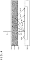
- FIG. 8 is a diagram for explaining the details of reflection at the BPF 205.
- FIG. 8 depicts first order diffractive reflection light Lr1, second order diffractive reflection light Lr2, third order diffractive reflection light Lr3, and fourth order diffractive reflection light Lr4.
- the diffractive reflection lights Lr1, Lr2, Lr3, and Lr4 are reflected by the BPF 205, and become reentering lights Ri1, Ri2, Ri3, and Ri4, respectively, to reenter the light reception section 202a.
- a part of the diffractive reflection light Lr1 becomes transmission light Lt1 to transmit through the BPF 205, and the remaining part thereof is reflected by the BPF 205.
- the diffractive reflection lights Lr2, Lr3, and Lr4 having traveled through the transparent member 204 and having a reflection angle (the angle of entering the BPF 205) of 41° or greater are totally reflected by the BPF 205 because none of the light components of these lights transmit through the BPF 205.
- diffractive reflection light not having been totally reflected by the BPF 205 and having a reflection angle of less than 41° is also imaged at a point close to the entering point of the intense light (entering light Li), compared to the points where the light totally reflected by the BPF 205 are imaged. Therefore, such diffractive reflection light hardly affects the accuracy of distance measurement.
- the diffraction angle ⁇ of the m-th order diffractive reflection light which is reflected by the light reception section 202a is expressed by the above Expression (2).
- the distance, in the light reception section 202a, from the entering point of the entering light Li to the reentering point of the reentering light Ri2 is approximately 90 ⁇ m. That is, the second order diffractive reflection light is imaged at a point apart, by 30 pixels, from the position where the intense light has been imaged.
- the points where the first to third order diffractive reflection lights are imaged are included within the distance of 80 pixels from the point where the intense light has been imaged.
- the distance between the light reception section 202a and the BPF 205 can be made sufficiently small. Accordingly, in an image obtained by image capturing by the biometric authentication apparatus, ghost and flare caused by reentering light components can be arranged so as not to be superimposed on a subject which is a face authentication target. That is, high-precise distance measurement can be conducted even in intense light such as sunlight. As a result, precise biometric authentication can be performed.
- a cover glass 221 is provided between the solid state imaging device 200 and the camera lens OP in the example in FIGS. 10 and 11 .
- An antireflection layer 222 is formed on the lower surface (image sensor 202-side surface) of the cover glass 221.
- an adjustment film 223 is formed on the upper surface (camera lens OP-side surface) of the cover glass 221.
- the BPF 205 is formed by vapor deposition on the surface of the transparent member 204, as previously explained.
- a bandpass filter formed by vapor deposition typically has such a transmission characteristic that a peak appears in a wavelength band apart from a stopband when a target wavelength that is intended to be transmitted through the filter is defined as a center wavelength ⁇ 0, as illustrated in FIG. 12 .
- a center wavelength ⁇ 0 as illustrated in FIG. 12 .
- the adjustment film 223 is formed so as to have a characteristic of prohibiting transmission of light of such a wavelength band.
- FIG. 13 illustrates an example of the transmission characteristics of the BPF 205 and the adjustment film 223.
- a peak appears at 940 nm which is the wavelength of infrared light intended to be transmitted through the BPF, and further, another peak appears near a wavelength ⁇ 1 which is apart from a stopband when 940 nm is set as the center wavelength. Consequently, not only infrared light but also light around the wavelength ⁇ 1 is transmitted through the BPF 205.
- the adjustment film 223 through which light of a wavelength band lower than a stopband of the BPF 205 and light of a wavelength band higher than the stopband of the BPF 205 are prohibited from transmitting is provided, any light other than infrared light can be inhibited from entering the image sensor 202. Accordingly, the accuracy of distance measurement is not degraded, and precise biometric authentication can be performed.
- FIG. 14 depicts an internal configuration example of the imaging camera 40 included in the distance measurement apparatus 1 according to the third embodiment of the present disclosure.
- the BPF 205 is formed on the light reception section 202a (imaging surface)-side surface of the transparent member 204.
- the abovementioned adjustment film 223 is formed on the subject-side surface (camera lens OP-side surface) of the transparent member 204.
- FIG. 15 depicts an internal configuration example of the imaging camera 40 included in the distance measurement apparatus 1 according to the fourth embodiment of the present disclosure.
- the transparent member 204 includes a cavity (void) 241 above the light reception section 202a of the image sensor 202.
- the BPF 205 is formed on the cavity 241-side surface (image sensor 202-side surface) of the transparent member 204.
- the abovementioned adjustment film 223 is formed on the subject-side surface (camera lens Op-side surface) of the transparent member 204.
- FIG. 16 depicts an internal configuration example of the imaging camera 40 included in the distance measurement apparatus 1 according to the fifth embodiment of the present disclosure.
- FIG. 17 depicts an internal configuration example of the imaging camera 40 included in the distance measurement apparatus 1 according to the sixth embodiment of the present disclosure.
- An adjustment film 306 is formed on the image sensor 302-side surface of the transparent member 305.
- a BPF 307 which is a transmission film that allows at least a peak wavelength band (930 to 950 nm) of infrared light to transmit therethrough and that cuts the remaining wavelength bands of infrared light, is formed on the subject-side surface (camera lens OP-side surface) of the transparent member 305.
- the distance measurement apparatus 1 having been explained so far is applicable not only to a biometric authentication apparatus, but also to various types of electronic apparatuses including image capturing apparatuses such as digital still cameras, digital video cameras, monitoring cameras, and on-vehicle cameras, camera-equipped mobile phones having distance measuring functions, and any other apparatuses having distance measuring functions.
- image capturing apparatuses such as digital still cameras, digital video cameras, monitoring cameras, and on-vehicle cameras, camera-equipped mobile phones having distance measuring functions, and any other apparatuses having distance measuring functions.
- FIG. 18 is a block diagram depicting a configuration example of an electronic apparatus to which the technology according to the present disclosure is applied.
- An electronic apparatus 500 depicted in FIG. 18 includes an optical system 501, a shutter device 502, a solid state imaging device 503, a control circuit 504, a signal processing circuit 505, a monitor 506, and a memory 507.
- the electronic apparatus 500 is capable of capturing still images and video images.
- the signal processing circuit 505 performs various signal processes on the signal charges outputted from the solid state imaging device 503.
- An image (image data) obtained as a result of the signal processes performed by the signal processing circuit 505 is supplied to the monitor 506 and is displayed thereon, or is supplied to the memory 507 and is saved (recorded) therein.
- high-precise distance measurement can be conducted even in intense light such as sunlight with the abovementioned solid state imaging device 200 or 300 applied to the optical system 501 and the solid state imaging device 503.
Landscapes
- Engineering & Computer Science (AREA)
- Physics & Mathematics (AREA)
- General Physics & Mathematics (AREA)
- Theoretical Computer Science (AREA)
- Optics & Photonics (AREA)
- Computer Security & Cryptography (AREA)
- Multimedia (AREA)
- Signal Processing (AREA)
- Computer Vision & Pattern Recognition (AREA)
- Computer Hardware Design (AREA)
- Software Systems (AREA)
- General Engineering & Computer Science (AREA)
- Toxicology (AREA)
- Health & Medical Sciences (AREA)
- Radar, Positioning & Navigation (AREA)
- Remote Sensing (AREA)
- Measurement Of Optical Distance (AREA)
- Image Input (AREA)
Abstract
Description
- The present disclosure relates to a distance measurement apparatus and a biometric authentication apparatus, and more particularly, to a distance measurement apparatus and a biometric authentication apparatus that are capable of conducting high-precise distance measurement even in intense light such as sunlight.
- In recent years, biometric authentication involving distance measurement has been popularly performed in order to prevent spoofing and fraud in mobile terminal devices equipped with cameras or in electronic settlement systems in banks, etc.
- To achieve downsizing, thickness reduction, and performance improvement of a biometric authentication apparatus for performing biometric authentication involving distance measurement, a method including generating diffraction light from collimated light/infrared light, imaging reflection light resulting from application of the diffraction light to a subject, and analyzing the obtained image of the subject has been used.
- Meanwhile, to achieve downsizing and thickness reduction of an image capturing apparatus, it has been known to use a solid state imaging element having a CSP (Chip Size Package) structure. For example, PTL 1 discloses a CSP solid state imaging element in which the upper surface portion of a glass wafer is coated with an IR cut filter layer.
- [PTL 1]
JP 2007-73958A - In a case where light reflected by a subject is imaged by a biometric authentication apparatus, if an image of the subject is captured in intense light such as sunlight (hereinafter, referred to as intense light), ghost and flare occur due to reflection of the intense light by an imaging surface of a solid state imaging element. This degrades the accuracy of distance measurement, so that there is a possibility that precise biometric authentication cannot be performed.
- The present disclosure has been achieved in view of the above circumstances, and enables high-precise distance measurement even in intense light such as sunlight.
- A distance measurement apparatus according to the present disclosure includes a light source that applies light to a subject, an image sensor that captures an image of the subject, a distance measurement section that calculates a distance to the subject on the basis of the image obtained by the image capturing, and a transparent member that is formed, on the image sensor, so as to be integrated with the image sensor. The transparent member includes a transmission film that allows a peak wavelength band of the light of the light source to transmit therethrough.
- A biometric authentication apparatus according to the present disclosure includes a light source that applies light to a subject, an image sensor that captures an image of the subject, a distance measurement section that calculates a distance to the subject on the basis of the image obtained by the image capturing, and a transparent member that is formed, on the image sensor, so as to be integrated with the image sensor. The transparent member includes a transmission film that allows a peak wavelength band of the light of the light source to transmit therethrough.
- The present disclosure includes the light source that applies light to a subject, the image sensor that captures an image of the subject, the distance measurement section that calculates the distance to the subject on the basis of the image obtained by the image capturing, and the transparent member that is formed, on the image sensor, so as to be integrated with the image sensor. The transparent member includes the transmission film that allows a peak wavelength band of the light of the light source to transmit therethrough.
-
- [
FIG. 1 ]
FIG. 1 is a diagram depicting a configuration example of a distance measurement apparatus according to an embodiment of the present disclosure. - [
FIG. 2 ]
FIG. 2 is an explanatory diagram of problems in an existing distance measurement apparatus. - [
FIG. 3 ]
FIG. 3 is a diagram illustrating an example of transmission characteristics of a BPF. - [
FIG. 4 ]
FIG. 4 is a diagram for explaining details of reflection at a BPF. - [
FIG. 5 ]
FIG. 5 depicts diagrams illustrating an example of ghost and flare. - [
FIG. 6 ]
FIG. 6 is a diagram for explaining reflection at a BPF. - [
FIG. 7 ]
FIG. 7 is a diagram depicting an internal configuration example of an imaging camera included in a distance measurement apparatus according to a first embodiment. - [
FIG. 8 ]
FIG. 8 is a diagram for explaining details of reflection at a BPF. - [
FIG. 9 ]
FIG. 9 depicts diagrams illustrating an example of ghost and flare. - [
FIG. 10 ]
FIG. 10 is a diagram depicting an internal configuration example of an imaging camera included in a distance measurement apparatus according to a second embodiment. - [
FIG. 11 ]
FIG. 11 is a diagram for explaining details of reflection at a BPF. - [
FIG. 12 ]
FIG. 12 is an explanatory diagram of stopbands. - [
FIG. 13 ]
FIG. 13 is a diagram illustrating an example of transmission characteristics of a BPF and an adjustment film. - [
FIG. 14 ]
FIG. 14 is a diagram depicting an internal configuration example of an imaging camera included in a distance measurement apparatus according to a third embodiment. - [
FIG. 15 ]
FIG. 15 is a diagram depicting an internal configuration example of an imaging camera included in a distance measurement apparatus according to a fourth embodiment. - [
FIG. 16 ]
FIG. 16 is a diagram depicting an internal configuration example of an imaging camera included in a distance measurement apparatus according to a fifth embodiment. - [
FIG. 17 ]
FIG. 17 is a diagram depicting an internal configuration example of an imaging camera included in a distance measurement apparatus according to a sixth embodiment. - [
FIG. 18 ]
FIG. 18 is a block diagram depicting a configuration example of an electronic apparatus. - Hereinafter, modes for carrying out the present disclosure (hereinafter, referred to as embodiments) will be explained. It is to be noted that the explanation will be given in the following order.
- 1. Configuration of Distance Measurement Apparatus
- 2. Problems in Existing Distance Measurement Apparatus
- 3. First Embodiment
- 4. Second Embodiment
- 5. Third Embodiment
- 6. Fourth Embodiment
- 7. Fifth Embodiment
- 8. Sixth Embodiment
- 9. Configuration Example of Electronic Apparatus
-
FIG. 1 is a diagram illustrating a configuration example of a distance measurement apparatus according to an embodiment of the present disclosure. - A distance measurement apparatus 1 depicted in
FIG. 1 generates diffraction light from infrared light, images reflection light resulting from application of the diffraction light to a subject SB, and calculates the distance to the subject SB by analyzing the obtained image of the subject. The distance measurement apparatus 1 is configured as a biometric authentication apparatus that performs face authentication of the subject SB by conducting distance measurement. - The distance measurement apparatus 1 includes a
light source 10, acorrection lens 20, a diffractive optical element (DOE) 30, animaging camera 40, and adistance measurement section 50. - The
light source 10 emits infrared light. Thecorrection lens 20 causes the infrared light of thelight source 10 to perpendicularly enter the diffractiveoptical element 30. - The diffractive
optical element 30 generates diffraction light from the light of thelight source 10 which thecorrection lens 20 has caused to enter the diffractiveoptical element 30. The subject SB is irradiated with the diffraction light emitted from the diffractiveoptical element 30. - The
imaging camera 40 captures an image of the subject SB being irradiated with the diffraction light, and supplies the obtained image (image data) to thedistance measurement section 50. - By analyzing the image data supplied from the
imaging camera 40, thedistance measurement section 50 calculates distance information which indicates the distance to the subject SB or indicates recesses and projections of the subject SB. The distance information calculated by thedistance measurement section 50 is used for face authentication of the subject SB. -
FIG. 2 depicts an internal configuration example of an imaging camera included in an existing distance measurement apparatus. - The imaging camera includes a solid
state imaging device 100. The solidstate imaging device 100 images infrared light that has been reflected by a subject and has entered the solidstate imaging device 100 through a camera lens OP. - The solid
state imaging device 100 includes asubstrate 101, a CMOS (Complementary Metal Oxide Semiconductor) image sensor 102 (hereinafter, simply referred to as an image sensor 102), and awire 103. Theimage sensor 102 may include a CCD (Charge-Coupled Device) image sensor. - The
image sensor 102 includes alight reception section 102a forming an imaging surface in which pixels are arranged in a matrix form. Respective bonding pads of thesubstrate 101 and theimage sensor 102 are connected via thewire 103, so that thesubstrate 101 and theimage sensor 102 are electrically connected. - In addition, a
cover glass 121 is disposed above theimage sensor 102. Anantireflection layer 122 is formed on the lower surface (image sensor 102-side surface) of thecover glass 121. A bandpass filter (hereinafter, referred to as BPF) 123, which is a transmission film that allows a peak wavelength band of infrared light to transmit therethrough and that cuts the remaining bands of infrared light, is formed on the upper surface (camera lens OP-side surface) of thecover glass 121. - With such a configuration, the solid
state imaging device 100 can image infrared light reflected by a subject. - In a case where light reflected by a subject is imaged with the configuration depicted in
FIG. 1 , if an image of the subject is captured in intense light such as sunlight, ghost and flare occur due to reflection of the intense light by thelight reception section 102a of theimage sensor 102. - That is, as illustrated in
FIG. 1 , entering light Li having a wavelength component of 940 nm included in the intense light having passed through the camera lens OP transmits through theBPF 123, and enters thelight reception section 102a of theimage sensor 102. Reflection light Lr resulting from diffractive reflection of the entering light Li by thelight reception section 102a enters theBPF 123, and a part of the reflection light Lr becomes transmission light Lt to transmit through theBPF 123 while the remaining part thereof is reflected by theBPF 123 and becomes reentering light Ri to reenter thelight reception section 102a. - Meanwhile, the transmission characteristic of the
BPF 123 varies according to the entering angle of the infrared light. - As illustrated in
FIG. 3 , for example, the transmission characteristic of theBPF 123 when the entering angle of the infrared light is 0° is different from that when the entering angle is 30°. Specifically, when the entering angle is 0°, light of 930 to 950 nm is transmitted through theBPF 123, and when the entering angle is 30°, light of 920 to 940 nm is transmitted through theBPF 123. - Due to the transmission characteristics of the
BPF 123, a light component, which is hatched inFIG. 3 , of the reflection light Lr resulting from diffractive reflection by thelight reception section 102a is reflected by theBPF 123, and becomes the reentering light Ri to reenter thelight reception section 102a. - Further, the reflection light Lr resulting from the diffractive reflection enters the
BPF 123 at an angle which depends on the order of diffraction. -
FIG. 4 is a diagram for explaining the details of reflection at theBPF 123. -
FIG. 4 depicts first order diffractive reflection light Lr1, second order diffractive reflection light Lr2, and third order diffractive reflection light Lr3. The diffractive reflection light Lr1, the diffractive reflection light Lr2, and the diffractive reflection light Lr3 are reflected by theBPF 123, and become reentering light Ri1, reentering light Ri2, and reentering light Ri3, respectively, to reenter thelight reception section 102a. - Accordingly, in an image obtained by image capturing, ghost and flare occur in a wide range GF1 centered on the intense light, as illustrated in A of
FIG. 5 . As a result, ghost and flare caused by the reentering light components are superimposed on a subject which is a face authentication target, as illustrated in B ofFIG. 5 . In this case, the accuracy of distance measurement is degraded, so that there is a possibility that precise biometric authentication cannot be performed. It is to be noted that, in the image illustrated in B ofFIG. 5 , white circles each indicate the 0-th order diffraction light of diffraction light applied to the subject, and black circles each indicate the first or higher order diffraction light. - Alternatively, the
BPF 123 may be formed not on the upper surface of thecover glass 121 but on the lower surface (image sensor 102-side surface) of thecover glass 121, as depicted inFIG. 6 . With such a structure, the distances which the diffractive reflection lights Lr1, Lr2, and Lr3 respectively travel before being reflected by theBPF 123 are shortened because the distance between thelight reception section 102a and the BPF 23 is shortened. Accordingly, the reentering points of the reentering lights Ri1, Ri2, and Ri3 in thelight reception section 102a are made close to the entering point of the entering light Li. As a result, in an image obtained by image capturing, ghost and flare caused by the reentering light components can be arranged so as not to be superimposed on a subject which is a face authentication target. - However, in the structure in which the
substrate 101 and theimage sensor 102 are electrically connected via thewire 103, there is a limit in shortening the distance between thelight reception section 102a and theBPF 123. - Specifically, the height of the
wire 103 from a surface of the image sensor 102 (light reception section 102a) is normally set to approximately 300 µm, and the distance between thelight reception section 102a and theBPF 123 is set to approximately 400 µm in view of manufacturing tolerance. - Here, when a refractive index n, a lattice constant d, a diffraction angle θ, a light wavelength λ, and an order m are given, the m-th order diffraction light has a relation of Expression (1) which is obtained by a Young's interference experiment.

- If the pixel pitch (corresponding to the lattice constant) d in the
light reception section 102a = 3 µm, the wavelength λ of infrared light = 940 nm, and the refractive index n of air = 1, for example, the diffraction angle θ of the m-th order diffractive reflection light which is reflected by thelight reception section 102a is expressed by Expression (2), on the basis of Expression (1).
- Therefore, in accordance with Expression (2), the diffraction angle θ of the m-th order diffractive reflection light (m = 1) is approximately 18.26°. In a case where the distance between the
light reception section 102a and theBPF 123 is 400 µm, the distance, in thelight reception section 102a, from the entering point of the entering light Li to the reentering point of the reentering light Ri1 is approximately 264 µm. That is, the first order diffractive reflection light is imaged at a point apart, by 88 pixels, from the position where the intense light has been imaged. - Further, in accordance with Expression (2), the diffraction angle θ of the second order diffractive reflection light (m = 2) is approximately 38.80°. In a case where the distance between the
light reception section 102a and theBPF 123 is 400 µm, the distance, in thelight reception section 102a, from the entering point of the entering light Li to the reentering point of the reentering light Ri2 is approximately 644 µm. That is, the second order diffractive reflection light is imaged at a point apart, by 214 pixels, from the position where the intense light has been imaged. - Likewise, in accordance with Expression (2), the diffraction angle θ of the third order diffractive reflection light (m = 3) is approximately 70.05°. In a case where the distance between the
light reception section 102a and theBPF 123 is 400 µm, the distance, in thelight reception section 102a, from the entering point of the entering light Li to the reentering point of the reentering light Ri3 is approximately 2204 µm. That is, the third order diffractive reflection light is imaged at a point apart, by 734 pixels, from the position where the intense light has been imaged. - Consequently, even with the structure depicted in
FIG. 6 , the distance between thelight reception section 102a and theBPF 123 cannot be made sufficiently short. As a result, there is a possibility that, in an image obtained by image capturing by the biometric authentication apparatus, ghost and flare caused by reentering light components are superimposed on a subject which is a face authentication target. - Thus, an explanation will be given below of embodiments in which the distance between a light reception section and a BPF is made sufficiently short to enable high-precise distance measurement even in intense light such as sunlight and precise biometric authentication can be performed.
-
FIG. 7 depicts an internal configuration example of theimaging camera 40 included in the distance measurement apparatus 1 according to the first embodiment of the present disclosure. - The
imaging camera 40 includes a solidstate imaging device 200. The solidstate imaging device 200 images infrared light that has been reflected by a subject and entered the solidstate imaging device 200 through the camera lens OP. - The solid
state imaging device 200 includes asubstrate 201 and animage sensor 202. Theimage sensor 202 is fixed on thesubstrate 201 while being electrically connected to thesubstrate 201. Theimage sensor 202 includes alight reception section 202a forming an imaging surface in which pixels are arranged in a matrix form. Theimage sensor 202 may include a CMOS image sensor or may include a CCD image sensor. - A
transparent member 204 that is formed of a glass substrate, for example, is bonded to theimage sensor 202 with a transparentadhesive resin 203. Accordingly, thetransparent member 204 is integrated with theimage sensor 202. That is, theimage sensor 202 has a CSP (Chip Size Package) structure. It is to be noted that the refractive index of theadhesive resin 203 is set to be substantially equal to that of thetransparent member 204. In addition, thetransparent member 204 may be formed of a material other than the glass substrate. - A bandpass filter (BPF) 205, which is a transmission film that allows at least a peak wavelength band (930 to 950 nm) of infrared light to transmit therethrough and that cuts the remaining wavelength bands of infrared light, is formed on the subject-side surface (camera lens OP-side surface) of the
transparent member 204. TheBPF 205 is formed by vapor deposition on the surface of thetransparent member 204. - With such a configuration, the solid
state imaging device 200 can image infrared light reflected by a subject. - In a case where light reflected by a subject is imaged with the configuration depicted in
FIG. 7 , if an image of the subject is captured in intense light such as sunlight, entering light Li of an infrared light component included in the intense light having passed through the camera lens OP transmits through theBPF 205, and enters thelight reception section 202a of theimage sensor 202. Reflection light Lr resulting from diffractive reflection of the entering light Li by thelight reception section 202a enters theBPF 205. A part of the reflection light Lr becomes transmission light Lt to transmit through theBPF 205 and go out into the air layer while the remaining part thereof is reflected by theBPF 205 and becomes reentering light Ri to reenter thelight reception section 202a. -
FIG. 8 is a diagram for explaining the details of reflection at theBPF 205. -
FIG. 8 depicts first order diffractive reflection light Lr1, second order diffractive reflection light Lr2, third order diffractive reflection light Lr3, and fourth order diffractive reflection light Lr4. The diffractive reflection lights Lr1, Lr2, Lr3, and Lr4 are reflected by theBPF 205, and become reentering lights Ri1, Ri2, Ri3, and Ri4, respectively, to reenter thelight reception section 202a. - In the example in
FIG. 8 , particularly, a part of the diffractive reflection light Lr1 becomes transmission light Lt1 to transmit through theBPF 205, and the remaining part thereof is reflected by theBPF 205. On the other hand, the diffractive reflection lights Lr2, Lr3, and Lr4 having traveled through thetransparent member 204 and having a reflection angle (the angle of entering the BPF 205) of 41° or greater are totally reflected by theBPF 205 because none of the light components of these lights transmit through theBPF 205. - In such a manner, the diffractive reflection lights having been reflected by the
light reception section 202a and having a reflection angle of 41° or greater are totally reflected by theBPF 205 without going out of thetransparent member 204 into the air layer. The lights totally reflected by theBPF 205 are received by thelight reception section 202a. If the thickness of the transparent member 204 (the distance between thelight reception section 202a and the BPF 205) is approximately 50 to 300 µm, for example, the lights are imaged at respective points close to the entering point of the intense light (entering light Li). The distance between thelight reception section 202a and theBPF 205 can be set to at least less than 400 µm. In the example inFIG. 8 , the distance is 100 µm. - Accordingly, in an image obtained by image capturing, ghost and flare occur within a range GF2 that is extremely close to the intense light, as illustrated in A of
FIG. 9 . However, as illustrated in B ofFIG. 9 , the ghost and flare caused by the totally reflected light components are not superimposed on a subject which is a face authentication target. Therefore, the accuracy of distance measurement is not degraded, and precise biometric authentication can be performed. - In addition, diffractive reflection light not having been totally reflected by the
BPF 205 and having a reflection angle of less than 41° is also imaged at a point close to the entering point of the intense light (entering light Li), compared to the points where the light totally reflected by theBPF 205 are imaged. Therefore, such diffractive reflection light hardly affects the accuracy of distance measurement. - For example, when the pixel pitch d in the
light reception section 202a = 3 µm, the wavelength λ of infrared light = 940 nm, and the refractive index n of theadhesive resin 203 and thetransparent member 204 = 1.51, the diffraction angle θ of the m-th order diffractive reflection light which is reflected by thelight reception section 202a is expressed by the above Expression (2). - Therefore, in accordance with Expression (2), the diffraction angle θ of the first order diffractive reflection light is approximately 12.06°. In a case where the distance between the
light reception section 202a and theBPF 205 is 100 µm, the distance, in thelight reception section 202a, from the entering point of the entering light Li to the reentering point of the reentering light Ri1 is approximately 42 µm. That is, the first order diffractive reflection light is imaged at a point apart, by 14 pixels, from the position where the intense light has been imaged. - Further, in accordance with Expression (2), the diffraction angle θ of the second order diffractive reflection light (m = 2) is approximately 24.69°. In a case where the distance between the
light reception section 202a and theBPF 205 is 100 µm, the distance, in thelight reception section 202a, from the entering point of the entering light Li to the reentering point of the reentering light Ri2 is approximately 90 µm. That is, the second order diffractive reflection light is imaged at a point apart, by 30 pixels, from the position where the intense light has been imaged. - Likewise, in accordance with Expression (2), the diffraction angle θ of the third order diffractive reflection light (m = 3) is approximately 38.80°. In a case where the distance between the
light reception section 202a and theBPF 205 is 100 µm, the distance, in thelight reception section 202a, from the entering point of the entering light Li to the reentering point of the reentering light Ri3 is approximately 160 µm. That is, the third order diffractive reflection light is imaged at a point apart, by 54 pixels, from the position where the intense light has been imaged. - In such a manner, the points where the first to third order diffractive reflection lights are imaged are included within the distance of 80 pixels from the point where the intense light has been imaged.
- In the past, the configuration in which an IR cut filter is provided to a transparent member formed integrally with an image sensor has been known, as disclosed in PTL 1. However, in a biometric authentication apparatus for performing biometric authentication involving distance measurement, providing a BPF that allows infrared light to pass therethrough to a transparent member formed integrally with an image sensor has not been considered.
- In the distance measurement apparatus 1 according to the present embodiment, since the
BPF 205 is formed on thetransparent member 204 that is formed integrally with theimage sensor 202, the distance between thelight reception section 202a and theBPF 205 can be made sufficiently small. Accordingly, in an image obtained by image capturing by the biometric authentication apparatus, ghost and flare caused by reentering light components can be arranged so as not to be superimposed on a subject which is a face authentication target. That is, high-precise distance measurement can be conducted even in intense light such as sunlight. As a result, precise biometric authentication can be performed. -
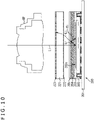
FIGS. 10 and11 each depict an internal configuration example of theimaging camera 40 included in the distance measurement apparatus 1 according to the second embodiment of the present disclosure. - In addition to configurations similar to those in
FIGS. 7 and8 , acover glass 221 is provided between the solidstate imaging device 200 and the camera lens OP in the example inFIGS. 10 and11 . - An
antireflection layer 222 is formed on the lower surface (image sensor 202-side surface) of thecover glass 221. On the other hand, anadjustment film 223 is formed on the upper surface (camera lens OP-side surface) of thecover glass 221. - The
BPF 205 is formed by vapor deposition on the surface of thetransparent member 204, as previously explained. A bandpass filter formed by vapor deposition typically has such a transmission characteristic that a peak appears in a wavelength band apart from a stopband when a target wavelength that is intended to be transmitted through the filter is defined as a center wavelength λ0, as illustrated inFIG. 12 . In order to suppress such a peak, it is necessary to perform vapor deposition or the like in a tank filled with hydrogen. This incurs a great increase in cost. - To this end, the
adjustment film 223 is formed so as to have a characteristic of prohibiting transmission of light of such a wavelength band. -
FIG. 13 illustrates an example of the transmission characteristics of theBPF 205 and theadjustment film 223. - In
FIG. 13 , a transmission characteristic C205 of theBPF 205 is indicated by a solid line, and a transmission characteristic C223 of theadjustment film 223 is indicated by a dotted line. - In the transmission characteristic C205, a peak appears at 940 nm which is the wavelength of infrared light intended to be transmitted through the BPF, and further, another peak appears near a wavelength λ1 which is apart from a stopband when 940 nm is set as the center wavelength. Consequently, not only infrared light but also light around the wavelength λ1 is transmitted through the
BPF 205. - On the other hand, in the transmission characteristic C223, light of a wavelength band including the wavelength λ1 is prohibited from transmitting through the adjustment film 223 (is cut).
- That is, a combination of the
BPF 205 and theadjustment film 223 has a transmission characteristic Cmix indicated by a dot-dash line inFIG. 13 . In the transmission characteristic Cmix, transmission of only the peak wavelength of infrared light is allowed, and the remaining wavelengths of infrared light including the wavelength λ1 are cut. - Therefore, since the
adjustment film 223 through which light of a wavelength band lower than a stopband of theBPF 205 and light of a wavelength band higher than the stopband of theBPF 205 are prohibited from transmitting is provided, any light other than infrared light can be inhibited from entering theimage sensor 202. Accordingly, the accuracy of distance measurement is not degraded, and precise biometric authentication can be performed. -
FIG. 14 depicts an internal configuration example of theimaging camera 40 included in the distance measurement apparatus 1 according to the third embodiment of the present disclosure. - In the configuration in
FIG. 14 , theBPF 205 is formed on thelight reception section 202a (imaging surface)-side surface of thetransparent member 204. In addition, theabovementioned adjustment film 223 is formed on the subject-side surface (camera lens OP-side surface) of thetransparent member 204. - It is to be noted that, in the configuration in
FIG. 14 , theBPF 205 needs to be formed on the surface of thetransparent member 204 before thetransparent member 204 is bonded to theimage sensor 202 with the transparentadhesive resin 203. - Since the
BPF 205 is formed on thelight reception section 202a-side surface of thetransparent member 204 in such a manner, the distance between thelight reception section 202a and theBPF 205 can be made extremely short. Accordingly, in an image obtained by image capturing by the biometric authentication apparatus, ghost and flare caused by reentering light components can be arranged so as not to be superimposed on a subject which is a face authentication target. That is, high-precise distance measurement can be conducted even in intense light such as sunlight. As a result, precise biometric authentication can be performed. -
FIG. 15 depicts an internal configuration example of theimaging camera 40 included in the distance measurement apparatus 1 according to the fourth embodiment of the present disclosure. - In the configuration in
FIG. 15 , thetransparent member 204 includes a cavity (void) 241 above thelight reception section 202a of theimage sensor 202. TheBPF 205 is formed on the cavity 241-side surface (image sensor 202-side surface) of thetransparent member 204. In addition, theabovementioned adjustment film 223 is formed on the subject-side surface (camera lens Op-side surface) of thetransparent member 204. - Since, in the configuration in which the
transparent member 204 includes the cavity 241 above thelight reception section 202a, theBPF 205 is formed on the cavity 241-side surface of thetransparent member 204 in such a manner, the distance between thelight reception section 202a and theBPF 205 can be made sufficiently short. Accordingly, in an image obtained by image capturing by the biometric authentication apparatus, ghost and flare caused by reentering light components can be arranged so as not to be superimposed on a subject which is a face authentication target. That is, high-precise distance measurement can be conducted even in intense light such as sunlight. As a result, precise biometric authentication can be performed. -
FIG. 16 depicts an internal configuration example of theimaging camera 40 included in the distance measurement apparatus 1 according to the fifth embodiment of the present disclosure. - Also in the configuration in
FIG. 16 , thetransparent member 204 includes the cavity 241 above thelight reception section 202a of theimage sensor 202. TheBPF 205 is formed on the subject-side surface (camera lens OP-side surface) of thetransparent member 204. In addition, theabovementioned adjustment film 223 is formed on the cavity 241-side surface (image sensor 202-side surface) of thetransparent member 204. - Since, in the configuration in which the
transparent member 204 includes the cavity 241 above thelight reception section 202a, theBPF 205 is formed on the subject-side surface of thetransparent member 204 in such a manner, the distance between thelight reception section 202a and theBPF 205 can be made sufficiently short. Accordingly, in an image obtained by image capturing by the biometric authentication apparatus, ghost and flare caused by reentering light components can be arranged so as not to be superimposed on a subject which is a face authentication target. That is, high-precise distance measurement can be conducted even in intense light such as sunlight. As a result, precise biometric authentication can be performed. -
FIG. 17 depicts an internal configuration example of theimaging camera 40 included in the distance measurement apparatus 1 according to the sixth embodiment of the present disclosure. - The
imaging camera 40 according to the present embodiment includes a solidstate imaging device 300. The solidstate imaging device 300 images incident infrared light having been reflected by a subject and having entered the solidstate imaging device 300 through the camera lens OP. - The solid
state imaging device 300 includes asubstrate 301, an image sensor 302, and awire 303. - The image sensor 302 includes a
light reception section 302a forming an imaging surface in which pixels are arranged in a matrix form. In addition, respective bonding pads of thesubstrate 301 and the image sensor 302 are connected via thewire 303, so that thesubstrate 301 and the image sensor 302 are electrically connected. - A
transparent member 305 that is formed of a glass substrate, for example, is bonded to the image sensor 302 with a transparentadhesive resin 304. Accordingly, thetransparent member 305 is integrated with the image sensor 302. - An
adjustment film 306 is formed on the image sensor 302-side surface of thetransparent member 305. In addition, aBPF 307, which is a transmission film that allows at least a peak wavelength band (930 to 950 nm) of infrared light to transmit therethrough and that cuts the remaining wavelength bands of infrared light, is formed on the subject-side surface (camera lens OP-side surface) of thetransparent member 305. - In the configuration in which the
substrate 301 and the image sensor 302 are connected via thewire 303, the image sensor 302 and thetransparent member 305 are integrally formed, and theBPF 307 is formed on the subject-side surface of thetransparent member 305 in such a manner. Therefore, the distance between thelight reception section 302a and theBPF 307 can be made sufficiently short. Accordingly, in an image obtained by image capturing by the biometric authentication apparatus, ghost and flare caused by reentering light components can be arranged so as not to be superimposed on a subject which is a face authentication target. That is, high-precise distance measurement can be conducted even in intense light such as sunlight. As a result, precise biometric authentication can be performed. - The distance measurement apparatus 1 having been explained so far is applicable not only to a biometric authentication apparatus, but also to various types of electronic apparatuses including image capturing apparatuses such as digital still cameras, digital video cameras, monitoring cameras, and on-vehicle cameras, camera-equipped mobile phones having distance measuring functions, and any other apparatuses having distance measuring functions.
-
FIG. 18 is a block diagram depicting a configuration example of an electronic apparatus to which the technology according to the present disclosure is applied. - An
electronic apparatus 500 depicted inFIG. 18 includes anoptical system 501, ashutter device 502, a solidstate imaging device 503, acontrol circuit 504, asignal processing circuit 505, amonitor 506, and amemory 507. Theelectronic apparatus 500 is capable of capturing still images and video images. - The
optical system 501 includes one or more lenses. Theoptical system 501 guides subject light (entering light) to the solidstate imaging device 503, and forms an image on a light reception section in the solidstate imaging device 503. - The
shutter device 502 is disposed between theoptical system 501 and the solidstate imaging device 503, and controls a time period for applying light to the solidstate imaging device 503 and a time period for blocking the light, under the control of thecontrol circuit 504. - The solid
state imaging device 503 includes a package including the abovementioned image sensor. The solidstate imaging device 503 accumulates signal charges during a fixed period of time according to light an image of which is formed on the light reception section via theoptical system 501 and theshutter device 502. The signal charges accumulated in the solidstate imaging device 503 are transferred according to a driving signal (timing signal) supplied from thecontrol circuit 504. - By outputting a driving signal for controlling a transfer operation of the solid
state imaging device 503 and a shutter operation of theshutter device 502, thecontrol circuit 504 drives the solidstate imaging device 503 and theshutter device 502. - The
signal processing circuit 505 performs various signal processes on the signal charges outputted from the solidstate imaging device 503. An image (image data) obtained as a result of the signal processes performed by thesignal processing circuit 505 is supplied to themonitor 506 and is displayed thereon, or is supplied to thememory 507 and is saved (recorded) therein. - Also with the
electronic apparatus 500 having the above configuration, high-precise distance measurement can be conducted even in intense light such as sunlight with the abovementioned solidstate imaging device optical system 501 and the solidstate imaging device 503. - It is to be noted that the embodiments of the present disclosure are not limited to the abovementioned embodiments, and various changes can be made within the scope of the gist of the present disclosure.
- In addition, the effects described herein are just examples, and effects to be provided by the present disclosure are not limited thereto. Any other effect may be provided.
- Furthermore, the present disclosure can have the following configurations.
- (1) A distance measurement apparatus including:
- a light source that applies light to a subject;
- an image sensor that captures an image of the subject;
- a distance measurement section that calculates a distance to the subject on the basis of the image obtained by the image capturing; and
- a transparent member that is formed, on the image sensor, so as to be integrated with the image sensor, in which
- the transparent member includes a transmission film that allows a peak wavelength band of the light of the light source to transmit therethrough.
- (2) The distance measurement apparatus according to (1), further including:
- a diffractive optical element that generates diffraction light from the light of the light source, in which
- the image sensor captures an image of the subject being irradiated with the diffraction light.
- (3) The distance measurement apparatus according to (2), further including:
a correction lens that causes the light of the light source to perpendicularly enter the diffractive optical element. - (4) The distance measurement apparatus according to any one of (1) to (3), in which
the light source emits infrared light. - (5) The distance measurement apparatus according to any one of (1) to (4), in which
- the transparent member is formed of a glass substrate that is bonded to the image sensor, and
- the image sensor has a CSP (Chip Size Package) structure.
- (6) The distance measurement apparatus according to (5), in which
the transmission film is formed on a subject-side surface of the transparent member. - (7) The distance measurement apparatus according to (5), in which
the transmission film is formed on an image sensor's imaging surface-side surface of the transparent member. - (8) The distance measurement apparatus according to (7), in which
- the transparent member includes a cavity above the imaging surface of the image sensor, and
- the transmission film is formed on a cavity-side surface of the transparent member.
- (9) The distance measurement apparatus according to any one of (5) to (8), in which
a distance between the imaging surface of the image sensor and the transmission film is set to be at least less than 400 µm. - (10) The distance measurement apparatus according to (9), in which
the distance between the imaging surface of the image sensor and the transmission film is set to fall within a range of 50 to 300 µm. - (11) The distance measurement apparatus according to any one of (1) to (10), further including:
an adjustment film through which light of a wavelength band lower than a stopband of the transmission film and/or light of a wavelength higher than a stopband of the transmission film is prohibited from transmitting. - (12) A biometric authentication apparatus including:
- a light source that applies light to a subject;
- an image sensor that captures an image of the subject;
- a distance measurement section that calculates a distance to the subject on the basis of the image obtained by the image capturing; and
- a transparent member that is formed, on the image sensor, so as to be integrated with the image sensor, in which
- the transparent member includes a transmission film that allows a peak wavelength of the light of the light source to transmit therethrough.
-
- 1: Distance measurement apparatus
- 10: Light source
- 20: Correction lens
- 30: Diffractive optical element
- 40: Imaging camera
- 200: Solid state imaging device
- 201: Substrate
- 202: Image sensor
- 202a: Light reception section
- 203: Adhesive resin
- 204: Transparent member
- 205: BPF
- 221: Cover glass
- 222: Antireflection layer
- 223: Adjustment film
- 241: Cavity
- 500: Electronic apparatus
- 503: Solid state imaging device
Claims (12)
- A distance measurement apparatus comprising:a light source that applies light to a subject;an image sensor that captures an image of the subject;a distance measurement section that calculates a distance to the subject on a basis of the image obtained by the image capturing; anda transparent member that is formed, on the image sensor, so as to be integrated with the image sensor, whereinthe transparent member includes a transmission film that allows a peak wavelength band of the light of the light source to transmit therethrough.
- The distance measurement apparatus according to claim 1, further comprising:a diffractive optical element that generates diffraction light from the light of the light source, whereinthe image sensor captures an image of the subject being irradiated with the diffraction light.
- The distance measurement apparatus according to claim 2, further comprising:
a correction lens that causes the light of the light source to perpendicularly enter the diffractive optical element. - The distance measurement apparatus according to claim 1, wherein
the light source emits infrared light. - The distance measurement apparatus according to claim 1, whereinthe transparent member is formed of a glass substrate that is bonded to the image sensor, andthe image sensor has a CSP (Chip Size Package) structure.
- The distance measurement apparatus according to claim 5, wherein
the transmission film is formed on a subject-side surface of the transparent member. - The distance measurement apparatus according to claim 5, wherein
the transmission film is formed on an image sensor's imaging surface-side surface of the transparent member. - The distance measurement apparatus according to claim 7, whereinthe transparent member includes a cavity above the imaging surface of the image sensor, andthe transmission film is formed on a cavity-side surface of the transparent member.
- The distance measurement apparatus according to claim 5, wherein
a distance between the imaging surface of the image sensor and the transmission film is set to be at least less than 400 µm. - The distance measurement apparatus according to claim 9, wherein
the distance between the imaging surface of the image sensor and the transmission film is set to fall within a range of 50 to 300 µm. - The distance measurement apparatus according to claim 1, further comprising:
an adjustment film through which light of a wavelength band lower than a stopband of the transmission film and/or light of a wavelength higher than a stopband of the transmission film is prohibited from transmitting. - A biometric authentication apparatus comprising:a light source that applies light to a subject;an image sensor that captures an image of the subject;a distance measurement section that calculates a distance to the subject on a basis of the image obtained by the image capturing; anda transparent member that is formed, on the image sensor, so as to be integrated with the image sensor, whereinthe transparent member includes a transmission film that allows a peak wavelength of the light of the light source to transmit therethrough.
Applications Claiming Priority (2)
| Application Number | Priority Date | Filing Date | Title |
|---|---|---|---|
| JP2019126689A JP2021012560A (en) | 2019-07-08 | 2019-07-08 | Distance measuring device and biometric authentication device |
| PCT/JP2020/024973 WO2021006050A1 (en) | 2019-07-08 | 2020-06-25 | Distance measurement device and biometric authentication device |
Publications (2)
| Publication Number | Publication Date |
|---|---|
| EP3998448A1 true EP3998448A1 (en) | 2022-05-18 |
| EP3998448A4 EP3998448A4 (en) | 2022-06-22 |
Family
ID=74114689
Family Applications (1)
| Application Number | Title | Priority Date | Filing Date |
|---|---|---|---|
| EP20836126.1A Withdrawn EP3998448A4 (en) | 2019-07-08 | 2020-06-25 | DISTANCE MEASURING DEVICE AND BIOMETRIC AUTHENTICATION DEVICE |
Country Status (4)
| Country | Link |
|---|---|
| US (1) | US20220309692A1 (en) |
| EP (1) | EP3998448A4 (en) |
| JP (1) | JP2021012560A (en) |
| WO (1) | WO2021006050A1 (en) |
Family Cites Families (11)
| Publication number | Priority date | Publication date | Assignee | Title |
|---|---|---|---|---|
| KR100738653B1 (en) | 2005-09-02 | 2007-07-11 | 한국과학기술원 | Wafer Level Chip Size Package for Image Sensor Module and Its Manufacturing Method |
| JP2009225064A (en) * | 2008-03-14 | 2009-10-01 | Ricoh Co Ltd | Image input device, authentication device, and electronic apparatus having them mounted thereon |
| JP5768396B2 (en) * | 2011-02-15 | 2015-08-26 | ソニー株式会社 | Solid-state imaging device, manufacturing method thereof, and electronic apparatus |
| CN110596806A (en) * | 2014-12-19 | 2019-12-20 | Agc株式会社 | Optical filter and device using the same |
| CN107438148B (en) * | 2016-05-27 | 2021-08-24 | 松下知识产权经营株式会社 | camera system |
| US10417473B2 (en) * | 2016-09-07 | 2019-09-17 | Mei-Yen Lee | Optical imaging system with variable light field for biometrics application |
| CN106778663B (en) * | 2016-12-29 | 2023-07-07 | 苏州塞罗尔医学影像科技有限公司 | Fingerprint identification system |
| JP2018200423A (en) * | 2017-05-29 | 2018-12-20 | ソニーセミコンダクタソリューションズ株式会社 | Imaging apparatus and electronic device |
| EP3683542B1 (en) * | 2017-09-13 | 2023-10-11 | Sony Group Corporation | Distance measuring module |
| CN109753852B (en) * | 2017-11-03 | 2020-09-18 | 华为技术有限公司 | Optical assembly for object texture, display assembly and electronic equipment |
| KR102481875B1 (en) * | 2017-12-27 | 2022-12-27 | 엘지디스플레이 주식회사 | Display device including fingerpring identification sensor |
-
2019
- 2019-07-08 JP JP2019126689A patent/JP2021012560A/en active Pending
-
2020
- 2020-06-25 US US17/597,163 patent/US20220309692A1/en not_active Abandoned
- 2020-06-25 EP EP20836126.1A patent/EP3998448A4/en not_active Withdrawn
- 2020-06-25 WO PCT/JP2020/024973 patent/WO2021006050A1/en not_active Ceased
Also Published As
| Publication number | Publication date |
|---|---|
| JP2021012560A (en) | 2021-02-04 |
| WO2021006050A1 (en) | 2021-01-14 |
| US20220309692A1 (en) | 2022-09-29 |
| EP3998448A4 (en) | 2022-06-22 |
Similar Documents
| Publication | Publication Date | Title |
|---|---|---|
| EP3133646A2 (en) | Sensor assembly with selective infrared filter array | |
| US11619772B2 (en) | Semiconductor chip and electronic apparatus | |
| EP3414763B1 (en) | Mobile device for hdr video capture | |
| US7119842B2 (en) | Image capturing device including a spectrally-selectively transmissive diaphragm | |
| US20070097249A1 (en) | Camera module | |
| CN102215349B (en) | Solid-state imaging device | |
| WO2017061296A1 (en) | Solid-state imaging element package, manufacturing method therefor, and electronic device | |
| US11569282B2 (en) | Image sensor package including bonding wire inside support member | |
| EP1906451A1 (en) | Imaging device | |
| EP1603165A2 (en) | Solid state imaging device, semiconductor wafer and camera module | |
| JP2017143092A (en) | Glass interposer module, imaging device, and electronic equipment | |
| US20210368080A1 (en) | Multi-cameras with shared camera apertures | |
| US20060092313A1 (en) | Image capturing apparatus | |
| EP1720340A1 (en) | Camera module | |
| US20200395396A1 (en) | Image sensor package | |
| US10451483B2 (en) | Short wave infrared polarimeter | |
| US11315966B2 (en) | Solid-state imaging element, manufacturing method, and electronic apparatus | |
| US20220309692A1 (en) | Distance measurement apparatus and biometric authentication apparatus | |
| US20190121005A1 (en) | Imaging device and filter | |
| JP2009217030A (en) | Optical system, and imaging device and digital apparatus using the optical system | |
| US6903774B2 (en) | Viewfinder device including first and second prisms to reflect light from outside the viewing area | |
| US12148777B2 (en) | Image sensor with spectral-filter-based crosstalk suppression | |
| JP5184244B2 (en) | Imaging device | |
| CN101071261A (en) | Method for detecting coated surface of IR-cut filter | |
| US10153314B2 (en) | Semiconductor apparatus, solid-state image pickup device, image pickup apparatus, and electronic apparatus |
Legal Events
| Date | Code | Title | Description |
|---|---|---|---|
| STAA | Information on the status of an ep patent application or granted ep patent |
Free format text: STATUS: THE INTERNATIONAL PUBLICATION HAS BEEN MADE |
|
| PUAI | Public reference made under article 153(3) epc to a published international application that has entered the european phase |
Free format text: ORIGINAL CODE: 0009012 |
|
| STAA | Information on the status of an ep patent application or granted ep patent |
Free format text: STATUS: REQUEST FOR EXAMINATION WAS MADE |
|
| 17P | Request for examination filed |
Effective date: 20211122 |
|
| AK | Designated contracting states |
Kind code of ref document: A1 Designated state(s): AL AT BE BG CH CY CZ DE DK EE ES FI FR GB GR HR HU IE IS IT LI LT LU LV MC MK MT NL NO PL PT RO RS SE SI SK SM TR |
|
| A4 | Supplementary search report drawn up and despatched |
Effective date: 20220519 |
|
| RIC1 | Information provided on ipc code assigned before grant |
Ipc: H04N 5/72 20060101ALI20220513BHEP Ipc: G01B 11/02 20060101ALI20220513BHEP Ipc: G06T 1/00 20060101ALI20220513BHEP Ipc: G01C 3/06 20060101ALI20220513BHEP Ipc: G01B 11/00 20060101AFI20220513BHEP |
|
| DAV | Request for validation of the european patent (deleted) | ||
| DAX | Request for extension of the european patent (deleted) | ||
| STAA | Information on the status of an ep patent application or granted ep patent |
Free format text: STATUS: EXAMINATION IS IN PROGRESS |
|
| 17Q | First examination report despatched |
Effective date: 20240119 |
|
| GRAP | Despatch of communication of intention to grant a patent |
Free format text: ORIGINAL CODE: EPIDOSNIGR1 |
|
| STAA | Information on the status of an ep patent application or granted ep patent |
Free format text: STATUS: GRANT OF PATENT IS INTENDED |
|
| RIC1 | Information provided on ipc code assigned before grant |
Ipc: G02B 5/18 20060101ALI20250115BHEP Ipc: G02B 27/00 20060101ALI20250115BHEP Ipc: G02B 5/20 20060101ALI20250115BHEP Ipc: G01C 15/00 20060101ALI20250115BHEP Ipc: G01C 3/06 20060101ALI20250115BHEP Ipc: G06T 1/00 20060101ALI20250115BHEP Ipc: G01B 11/02 20060101ALI20250115BHEP Ipc: H04N 5/72 20060101ALI20250115BHEP Ipc: G01B 11/00 20060101AFI20250115BHEP |
|
| INTG | Intention to grant announced |
Effective date: 20250123 |
|
| STAA | Information on the status of an ep patent application or granted ep patent |
Free format text: STATUS: THE APPLICATION IS DEEMED TO BE WITHDRAWN |
|
| 18D | Application deemed to be withdrawn |
Effective date: 20250524 |