EP3996281A1 - Analog-to-digital converter circuit, corresponding system and method - Google Patents
Analog-to-digital converter circuit, corresponding system and method Download PDFInfo
- Publication number
- EP3996281A1 EP3996281A1 EP21204292.3A EP21204292A EP3996281A1 EP 3996281 A1 EP3996281 A1 EP 3996281A1 EP 21204292 A EP21204292 A EP 21204292A EP 3996281 A1 EP3996281 A1 EP 3996281A1
- Authority
- EP
- European Patent Office
- Prior art keywords
- sensing
- digital
- adc
- analog
- error
- Prior art date
- Legal status (The legal status is an assumption and is not a legal conclusion. Google has not performed a legal analysis and makes no representation as to the accuracy of the status listed.)
- Pending
Links
- 238000000034 method Methods 0.000 title claims description 6
- 238000012545 processing Methods 0.000 claims abstract description 32
- 238000006243 chemical reaction Methods 0.000 claims abstract description 9
- 230000005540 biological transmission Effects 0.000 abstract description 13
- 101710096655 Probable acetoacetate decarboxylase 1 Proteins 0.000 abstract 1
- 108091022873 acetoacetate decarboxylase Proteins 0.000 abstract 1
- 230000006870 function Effects 0.000 description 12
- 238000005259 measurement Methods 0.000 description 12
- 238000010586 diagram Methods 0.000 description 6
- 230000005669 field effect Effects 0.000 description 5
- 230000008901 benefit Effects 0.000 description 4
- 238000010348 incorporation Methods 0.000 description 2
- 239000000463 material Substances 0.000 description 2
- 238000009529 body temperature measurement Methods 0.000 description 1
- 238000003745 diagnosis Methods 0.000 description 1
- 230000000694 effects Effects 0.000 description 1
- 239000011159 matrix material Substances 0.000 description 1
- 238000012544 monitoring process Methods 0.000 description 1
- 230000000737 periodic effect Effects 0.000 description 1
- 238000012502 risk assessment Methods 0.000 description 1
- 239000004065 semiconductor Substances 0.000 description 1
- 238000012360 testing method Methods 0.000 description 1
Images


Classifications
-
- H—ELECTRICITY
- H03—ELECTRONIC CIRCUITRY
- H03M—CODING; DECODING; CODE CONVERSION IN GENERAL
- H03M1/00—Analogue/digital conversion; Digital/analogue conversion
- H03M1/10—Calibration or testing
- H03M1/1004—Calibration or testing without interrupting normal operation, e.g. by providing an additional component for temporarily replacing components to be tested or calibrated
-
- H—ELECTRICITY
- H03—ELECTRONIC CIRCUITRY
- H03M—CODING; DECODING; CODE CONVERSION IN GENERAL
- H03M1/00—Analogue/digital conversion; Digital/analogue conversion
- H03M1/10—Calibration or testing
- H03M1/1071—Measuring or testing
-
- H—ELECTRICITY
- H03—ELECTRONIC CIRCUITRY
- H03M—CODING; DECODING; CODE CONVERSION IN GENERAL
- H03M1/00—Analogue/digital conversion; Digital/analogue conversion
- H03M1/06—Continuously compensating for, or preventing, undesired influence of physical parameters
- H03M1/0617—Continuously compensating for, or preventing, undesired influence of physical parameters characterised by the use of methods or means not specific to a particular type of detrimental influence
- H03M1/0675—Continuously compensating for, or preventing, undesired influence of physical parameters characterised by the use of methods or means not specific to a particular type of detrimental influence using redundancy
- H03M1/0678—Continuously compensating for, or preventing, undesired influence of physical parameters characterised by the use of methods or means not specific to a particular type of detrimental influence using redundancy using additional components or elements, e.g. dummy components
-
- H—ELECTRICITY
- H03—ELECTRONIC CIRCUITRY
- H03M—CODING; DECODING; CODE CONVERSION IN GENERAL
- H03M1/00—Analogue/digital conversion; Digital/analogue conversion
- H03M1/06—Continuously compensating for, or preventing, undesired influence of physical parameters
- H03M1/0617—Continuously compensating for, or preventing, undesired influence of physical parameters characterised by the use of methods or means not specific to a particular type of detrimental influence
- H03M1/0675—Continuously compensating for, or preventing, undesired influence of physical parameters characterised by the use of methods or means not specific to a particular type of detrimental influence using redundancy
- H03M1/0687—Continuously compensating for, or preventing, undesired influence of physical parameters characterised by the use of methods or means not specific to a particular type of detrimental influence using redundancy using fault-tolerant coding, e.g. parity check, error correcting codes
-
- H—ELECTRICITY
- H03—ELECTRONIC CIRCUITRY
- H03M—CODING; DECODING; CODE CONVERSION IN GENERAL
- H03M1/00—Analogue/digital conversion; Digital/analogue conversion
- H03M1/10—Calibration or testing
- H03M1/1071—Measuring or testing
- H03M1/1076—Detection or location of converter hardware failure, e.g. power supply failure, open or short circuit
-
- H—ELECTRICITY
- H03—ELECTRONIC CIRCUITRY
- H03M—CODING; DECODING; CODE CONVERSION IN GENERAL
- H03M1/00—Analogue/digital conversion; Digital/analogue conversion
- H03M1/12—Analogue/digital converters
- H03M1/1205—Multiplexed conversion systems
- H03M1/122—Shared using a single converter or a part thereof for multiple channels, e.g. a residue amplifier for multiple stages
- H03M1/1225—Shared using a single converter or a part thereof for multiple channels, e.g. a residue amplifier for multiple stages using time-division multiplexing
-
- H—ELECTRICITY
- H03—ELECTRONIC CIRCUITRY
- H03M—CODING; DECODING; CODE CONVERSION IN GENERAL
- H03M1/00—Analogue/digital conversion; Digital/analogue conversion
- H03M1/12—Analogue/digital converters
- H03M1/1205—Multiplexed conversion systems
- H03M1/123—Simultaneous, i.e. using one converter per channel but with common control or reference circuits for multiple converters
Definitions
- the description relates to safety checks in devices such as analog-to-digital converters (ADCs).
- ADCs analog-to-digital converters
- One or more embodiments may be applied in the automotive sector, for instance, in transmission control units and braking control units for current measurement in valve driver blocks.
- a high level of safety is desirable in integrated circuits (ICs) for use in transmission and braking applications in the automotive sector, for thermal sensors for instance.
- ICs integrated circuits
- the ASIL scheme is established by performing a risk analysis of a potential hazard by looking at the severity, exposure and controllability of the operating scenario of a vehicle.
- ASIL A There are currently four ASIL categories: ASIL A, ASIL B, ASIL C, ASIL D, where ASIL D dictates the highest integrity specification and ASIL A the dictates the lowest.
- a conventional implementation for thermal sensors is based on architecture comprising a small BJT (bipolar junction transistor) sensor in combination with a high-resolution ADC that converts a voltage signal proportional to temperature into a temperature code.
- BJT bipolar junction transistor
- thermal sensors may be configured, for instance, to measure a temperature in an IC die and currents in valve driver blocks and to provide real-time temperature information to an interpolator in order to achieve desired target accuracy.
- a whole measurement chain including a thermal sensor, may be rendered completely independent, which involves implementing a redundant "thermal" ADC, which results in twice-added (2x) complexity for each channel.
- An object of one or more embodiments is to address the issues outlined previously, while avoiding the added complexity discussed in the foregoing.
- One or more embodiments may relate to a corresponding system.
- a multi-channel valve drive system for use in transmission and braking applications in the automotive sector may be exemplary of such a system.
- One or more embodiments may relate to a corresponding method.
- One or more embodiments may advantageously provide architecture for measuring temperature in an IC die (in a valve driver block, for instance).
- an ADC is associated to a respective main temperature sensor for each channel and redundant temperature sensors are associated to a single shared ADC by means of a multiplexer.
- a "redundant" temperature measurement of each redundant sensor is provided in a corresponding time frame and real-time measurement of a main temperature sensor is provided so that N channels involve only N+1 ADCs.
- transmission control units and braking control units for automotive applications benefit from a high level of safety (up to ASIL-D), with a safe (alert) state asserted in case of malfunctioning of a component in the control unit.
- ASIL-D high level of safety
- a safe (alert) state asserted in case of malfunctioning of a component in the control unit.
- Such system level specifications are expected to be complied with by all the components in the control unit, especially by those ICs providing a basis for the whole system.
- such level of safety should desirably be reached for thermal sensors in the first place.
- FIG. 1 is block diagram exemplary of a conventional implementation for this kind of sensor arrangement comprising sensors S1, S2 (small CSA-certified - BJT sensors, for instance) for high-side (HS) and low-side (LS), respectively.
- the sensors S1 and S2 co-operate with (high-resolution) ADCs ADC HS and ADC LS that convert voltages proportional to the temperature as provided by the sensors S1 and S2 to a temperature code.
- Such thermal sensors can be configured to measure the die temperature of an integrated circuit IC (not visible in the figure) and for current measurement in valve driver blocks to provide real-time temperature to interpolators in order to facilitate achieving a target accuracy.
- a (single channel) measurement chain as illustrated in Figure 1 that is, including the sensors S1, S2, includes (completely) independent signal paths.
- an arrangement as illustrated in Figure 1 comprises:
- An arrangement as illustrated in Figure 1 also comprises a multiplexer 18 driven by an on-off (pulse-width modulated) signal PWM to alternately supply the outputs from the high-side branch and low-side branch discussed previously (essentially the outputs from the calibration circuitry 14H and 14L) to a controller 20 (for instance, a proportional-integral or PI controller) sensitive to a current set point CS and configured to generate the signal PWM.
- a controller 20 for instance, a proportional-integral or PI controller
- the (average) value of the output from the multiplexer 18 is indicative of the average current 18 provided by the high-side branch and low-side branch discussed previously and thus of the average value of the temperature sensed by the sensors S1 and S2 as indicated by the block 22.
- a PWM monitor circuit 24 receives a PWM feedback signal from the input analog channel in order to verify that such a PWM signal at the output of the valve driver is consistent - for instance, equal, with a certain margin of error - with the value imposed by the controller block 20 (a PI controller, for instance).
- Such a signal can be provided by an analog comparator that compares the output voltage with the voltage of the supply (battery). This may take place, for instance, with a threshold having a value which is half the battery value.
- the device may be configured to provide (on SPI registers, for instance) the duty cycle measured by the block 24 and a microcontroller - at the system level - can compare it with the theoretical values set by the block 20 (which can also be read from SPI registers). If the difference exceeds a certain threshold, the microcontroller may set the system to a "safe" state.
- comparator circuitry 26 can be coupled to the outputs from the high-side branch and low-side branch discussed previously (essentially the outputs from the calibration circuitry 14H and 14L) with the capability of comparing these two outputs (and thus the temperature values sensed by the sensors S1 and S2).
- the information provided by the block 24 is also used by the block 26 (high-side, low-side compare) for diagnostics purposes.
- Transmission control units (TCUs) and braking control units for automotive applications may involve a high multiplicity of architectures as illustrated in Figure 1 .
- N channels involve 2xN thermal sensors (more specifically, 2xN BJT sensors such as S1 and S2 plus 2xN ADCs such as ADC HS and ADC LS)
- FIG. 1 An arrangement as illustrated in Figure 1 involves HS and LS paths which are (completely) independent of each other in order to facilitate ASIL-D compliance as well as independent redundant current monitors (in order to facilitate HS-LS comparison at 26, for instance) plus independent temperature interpolators for the two paths.
- FIG. 2 is illustrative of an embodiment of a valve driver including N channels with High-Side (HS) and Low-Side (LS) field-effect transistors (FETs).
- HS High-Side
- LS Low-Side field-effect transistors
- Such a driver (which can otherwise retain certain features of the arrangement illustrated in Figure 1 ) can be incorporated, for instance, in a transmission control unit for passenger vehicles and (PVs) and commercial vehicles (CVs).
- Valve driver stages as implemented in transmission and braking control units are exemplary of such a possible application.
- One or more embodiments can in fact be generally applied to circuits where a high level of safety (up to ASIL-D, for instance) is desirable, which may result in redundancy for each function.
- such an ADC can be implemented in a redundant manner (which facilitates fulfilling ASIL-D requirements, for instance) by providing for "physical" redundancy of a (whole) ADC structure.
- One or more embodiments may achieve (full) redundancy via digital signal processing (thus without physical redundancy of a whole ADC), which provides benefits in terms in die size and test time saved and increased diagnosis coverage.
- Embodiments as illustrated in Figure 2 may comprise a number N of channels (channel 1 to channel N) each including (see the left-hand portion of the figure) two sensors S_CH_1, S_CN_1R to S_CH_N, S_CN_NR.
- These sensors can be, for instance, BJT (bipolar junction transistor) thermal sensors.
- BJT bipolar junction transistor
- Such an option may be advantageous due to its reduced contribution to thermal sensor area, especially if compared with the larger contribution to the whole thermal sensor area as provided by ADCs, only one of which, namely ADC_1 to ADC_N, is used for each channel as illustrated in Figure 2 .
- the sensors in each pair can be regarded as including a first sensor, S_CH_1 to S_CH_N, and a second sensor S_CN_1R to S_CN_NR providing safety redundancy in (e.g. temperature) sensing as indicated by SR.
- the outputs from the first sensors S_CH_1 to S_CH_N are applied to respective ADCs, namely ADC_1 to ADC_N, which may be configured to provide, for instance, analog sigma-delta quantizer and digital decimator functions.
- the outputs from the second, redundancy sensors S_CH_1R to S_CH_NR are applied to a single common ADC, namely ADC_R, which may likewise be configured to provide, for instance, analog sigma-delta quantizer and digital decimator functions.
- supplying the outputs from the redundancy sensors S_CH_1R to S_CH_NR to the analog-to-digital converter ADC_R is via a (first) multiplexer, MUX1.
- the multiplexer MUX1 is sensitive to a selector signal SS, which can be generated (in a manner known per se to those of skill in the art, via a time window selector circuit STW) to be indicative of a time window.
- the hardware of the analog-to-digital converter ADC R can be shared by the N channels, with each channel suited to be processed in a respective time window as discussed in the following.
- the analog (e.g. temperature) signals from the sensors S_CH_1 to S_CH_N and S_CH_1R to S_CH_NR are converted into corresponding digital signals (8-bit codes, for instance) TEMP_CODE_1 to TEMP_CODE_N (from the converters ADC_1 to ADC_N coupled individually to the sensors S_CH_1 to S_CH_N) and TEMP_CODE_RED (from the common converter ADC_R coupled to the sensors S_CH_1R to S_CH_NR via the multiplexer MUX1).
- TEMP_CODE_1 to TEMP_CODE_N from the converters ADC_1 to ADC_N coupled individually to the sensors S_CH_1 to S_CH_N
- TEMP_CODE_RED from the common converter ADC_R coupled to the sensors S_CH_1R to S_CH_NR via the multiplexer MUX1).
- References 101 and 102 denote two interpolators (HS and LS, respectively) that receive the digital signals TEMP_CODE_1 to TEMP_CODE_N from the converters, ADC_1 to ADC_N.
- the interpolators 101, 102 may be of any type known to those of skill in the art for a desired drive function of respective electrical loads such as field-effect transistors HS FET (high-side) and LS FET (low-side).
- the blocks 101, 102 may provide as an output an error value affecting the measurement of an actuation current supplied to a load associated with the respective channel, assumed to be at a certain temperature.
- Input to (each) block 101, 102 may comprise a matrix T(C) of current errors for certain temperature and current values taken as a reference, as possibly derived from a memory block (two RAM memory banks, for instance) not visible in the figures for simplicity.
- the blocks 101, 102 may be configured to calculate (in a manner known per se to those of skill in the art) an error value at a generic temperature and current by interpolating that error value starting from the reference values.
- a same block 101 may repeat the calculation scanning the N channels in a sequential manner.
- a same block may be replicated in 101 and 102 in order to provide an independent calculation for the high-side (HS) and the low-side (LS). In that way, two independent HS and LS measurements are available which can be compared to ascertain if any misalignments (errors) arise.
- HS high-side
- LS low-side
- both interpolators 101 and 102 use the same (temperature) sensors S_CH_1 to S_CH_N and analog-to-digital converters ADC_1 to ADC_N.
- such a redundant converter ADC R can be placed at an IC top level with the capability of multiplexing via the multiplexer MUX1 the signals from the redundant sensors S_CH_1R to S_CH_NR present in each one of the N channels for a time (as set via the signal SS) selected to provide an adequate (e.g. temperature) measurement and to facilitate fulfilling a desired FTTI (fault tolerant time interval).
- a digital processing circuit block 103 is configured to act as a safety ADC checker and compare the (temperature) values read by the "main" sensors S_CH_1 to S_CH_N with corresponding values read by the "redundant" sensors S_CH_1R to S_CH_NR.
- the values should be the same assuming that the main and redundant sensors are placed in corresponding positions (the same positions in a semiconductor die, for instance).
- the ADC checker circuit 103 has the purpose of revealing errors affecting any of the channels 1 to N and prompting adequate reaction (for instance setting the channel to a three-state turnoff/low-power condition).
- the safety ADC checker circuit 103 is configured to act on (to compare):
- operation of the multiplexers MUX1, MUX2 can be co-ordinated in such a way that, at a certain time window j (in a periodic sequence of N windows), the safety ADC checker circuit 103 compares:
- error signals error_CH_1 to error_CH_N may reveal errors affecting any of the channels 1 to N and prompt adequate reaction: for instance, the channel found affected by error being set to a three-state turnoff/low-power condition).
- error signals error_CH_1 to error_CH_N (which may indicate an inconsistency in the measurement of die temperature) can be transmitted from the circuit 100 (on a "fault" pin for instance) and/or be stored in internal registers which can be accessed by a microcontroller, for instance.
- Such mismatch errors in measuring temperature may apply both the valve channels and the die, that is, the N channel illustrated herein can be regarded as comprising both the valves and the die.
- One or more embodiments may include a temperature control function of the temperature of the whole die.
- one or more embodiments are in fact largely “transparent" to the intended use of both the signals from the blocks 101, 102 and the signals error_CH_1 to error_CH_N from the block 103.
- a circuit as illustrated in Figure 2 facilitates achieving independency to fulfill specifications such as ASIL-D requirement with reduce die size impact.
- a circuit as illustrated in Figure 2 and including N channels comprises N+1 analog-to-digital converters (ADC_1 to ADC_N plus ADC_R) and 2xN sensors (N main sensors S_CH_1 to S_CH_N and N redundant sensors S_CH_1R to S_CH_NR.
- ADC_1 to ADC_N plus ADC_R N+1 analog-to-digital converters
- 2xN sensors N main sensors S_CH_1 to S_CH_N and N redundant sensors S_CH_1R to S_CH_NR.
- FIG 3 is a block diagram exemplary of the possible incorporation of embodiments in a transmission control unit 1000 for passenger vehicles and (PVs) and commercial vehicles (CVs).
- PVs passenger vehicles and
- CVs commercial vehicles
- a transmission control unit 1000 as illustrated in Figure 3 may include various other blocks/elements which are per se conventional in the art and are not expressly mentioned and/or referenced insofar as they are not of specific importance for the embodiments.
- a circuit for instance, 100 as exemplified herein may comprise:
- said first and second digital processing circuitry coupled to said plurality of N analog-to-digital converters may be configured to perform interpolator digital processing on said N first digital signals as a function of a set of reference signals (for instance, T(C)) received at said first and second (102) digital processing circuitry.
- a circuit as exemplified may comprise:
- a circuit as exemplified herein may be configured to:
- each sensing channel in said plurality of N sensing channels may comprise at least one thermal sensor providing a temperature sensing signal to one of said first sensing node (for instance, S_CH_1 to S_CH_N) and said second sensing node (for instance, S_CH_1R to S_CH_NR) paired therewith.
- a circuit as exemplified herein may comprise a first sensor supplying a first sensing signal to said first sensing node and a second sensor providing a second sensing signal to said second sensing node paired therewith.
- a system for instance, a transmission control unit 1000 for passenger and commercial vehicles such as 1000
- a transmission control unit 1000 for passenger and commercial vehicles such as 1000 may comprise:
- a method of operating a circuit or a system as exemplified herein may comprise:
Landscapes
- Engineering & Computer Science (AREA)
- Theoretical Computer Science (AREA)
- Analogue/Digital Conversion (AREA)
Abstract
Description
- The description relates to safety checks in devices such as analog-to-digital converters (ADCs).
- One or more embodiments may be applied in the automotive sector, for instance, in transmission control units and braking control units for current measurement in valve driver blocks.
- A high level of safety is desirable in integrated circuits (ICs) for use in transmission and braking applications in the automotive sector, for thermal sensors for instance.
- Specifications such as ISO26262 - Functional Safety for Road Vehicles, define a risk classification scheme referred to as ASIL (Automotive Safety Integrity Level) which is helpful in defining safety specifications in line with ISO 26262.
- The ASIL scheme is established by performing a risk analysis of a potential hazard by looking at the severity, exposure and controllability of the operating scenario of a vehicle.
- There are currently four ASIL categories: ASIL A, ASIL B, ASIL C, ASIL D, where ASIL D dictates the highest integrity specification and ASIL A the dictates the lowest.
- A conventional implementation for thermal sensors is based on architecture comprising a small BJT (bipolar junction transistor) sensor in combination with a high-resolution ADC that converts a voltage signal proportional to temperature into a temperature code.
- These thermal sensors may be configured, for instance, to measure a temperature in an IC die and currents in valve driver blocks and to provide real-time temperature information to an interpolator in order to achieve desired target accuracy.
- Current measurement in valve driver blocks may benefit from (complete) independency of a low-side (LS) path and a high-side (HS) path.
- To that end, a whole measurement chain, including a thermal sensor, may be rendered completely independent, which involves implementing a redundant "thermal" ADC, which results in twice-added (2x) complexity for each channel.
- An object of one or more embodiments is to address the issues outlined previously, while avoiding the added complexity discussed in the foregoing.
- According to one or more embodiments, that object can be achieved by means of an analog-to-digital converter circuit having the features set forth in the claims that follow.
- One or more embodiments may relate to a corresponding system. A multi-channel valve drive system for use in transmission and braking applications in the automotive sector may be exemplary of such a system.
- One or more embodiments may relate to a corresponding method.
- The claims are an integral part of the technical teaching provided herein in respect of the embodiments.
- One or more embodiments may advantageously provide architecture for measuring temperature in an IC die (in a valve driver block, for instance).
- In comparison with the prior art (where N channels involve 2xN ADCs), in one or more embodiments, an ADC is associated to a respective main temperature sensor for each channel and redundant temperature sensors are associated to a single shared ADC by means of a multiplexer.
- In one or more embodiments, a "redundant" temperature measurement of each redundant sensor is provided in a corresponding time frame and real-time measurement of a main temperature sensor is provided so that N channels involve only N+1 ADCs.
- One or more embodiments will now be described, by way of example only, with reference to the annexed figures, wherein:
-
Figure 1 is a block diagram illustrative of an implementation of independent HS/LS current measurement paths, -
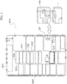
Figure 2 is a block diagram illustrative of a solution for a driver channel with a high-side FET and a low-side FET in valve driver according to embodiments as exemplified herein, and -
Figure 3 is a block diagram exemplary of the possible incorporation of embodiments in a transmission control unit. - In the ensuing description, one or more specific details are illustrated, aimed at providing an in-depth understanding of examples of embodiments of this description. The embodiments may be obtained without one or more of the specific details, or with other methods, components, materials, etc. In other cases, known structures, materials, or operations are not illustrated or described in detail so that certain aspects of embodiments will not be obscured.
- Reference to "an embodiment" or "one embodiment" in the framework of the present description is intended to indicate that a particular configuration, structure, or characteristic described in relation to the embodiment is comprised in at least one embodiment. Hence, phrases such as "in an embodiment" or "in one embodiment" that may be present in one or more points of the present description do not necessarily refer to one and the same embodiment.
- Moreover, particular conformations, structures, or characteristics may be combined in any adequate way in one or more embodiments.
- The headings/references used herein are provided merely for convenience and hence do not define the extent of protection or the scope of the embodiments.
- As discussed in the introductory portion of this description, transmission control units and braking control units for automotive applications benefit from a high level of safety (up to ASIL-D), with a safe (alert) state asserted in case of malfunctioning of a component in the control unit.
- Such system level specifications are expected to be complied with by all the components in the control unit, especially by those ICs providing a basis for the whole system. In an ASIL-D IC for transmission and braking applications, as considered herein by way of example, such level of safety should desirably be reached for thermal sensors in the first place.
-
Figure 1 is block diagram exemplary of a conventional implementation for this kind of sensor arrangement comprising sensors S1, S2 (small CSA-certified - BJT sensors, for instance) for high-side (HS) and low-side (LS), respectively. The sensors S1 and S2 co-operate with (high-resolution) ADCs ADC HS and ADC LS that convert voltages proportional to the temperature as provided by the sensors S1 and S2 to a temperature code. - Such thermal sensors can be configured to measure the die temperature of an integrated circuit IC (not visible in the figure) and for current measurement in valve driver blocks to provide real-time temperature to interpolators in order to facilitate achieving a target accuracy.
- In current measurement of valve driver blocks independency between LS and HS paths is desirable.
- For that reason, a (single channel) measurement chain as illustrated in
Figure 1 , that is, including the sensors S1, S2, includes (completely) independent signal paths. - Independent HS and LS paths as illustrated in
Figure 1 facilitate achieving compliance with ASIL-D specifications and independency of redundant current monitoring (with HS and LS comparable therebetween). - This in turn involves implementing independent temperature interpolation for the two paths (S1, ADC HS and S2, ADC LS) in a single analog channel as illustrated and an intrinsic redundancy of the temperature sensor arrangement.
- For instance, for a (single) digital channel to be coupled to an analog channel comprising two sensors S1, S2 and two ADCs, namely ADC HS and ADC LS, an arrangement as illustrated in
Figure 1 comprises: -
ADC logic circuitry 10H (high) and 10L (low), -
filter circuitry -
calibration circuitry calibration temperature sources - An arrangement as illustrated in
Figure 1 also comprises amultiplexer 18 driven by an on-off (pulse-width modulated) signal PWM to alternately supply the outputs from the high-side branch and low-side branch discussed previously (essentially the outputs from thecalibration circuitry - The (average) value of the output from the
multiplexer 18 is indicative of theaverage current 18 provided by the high-side branch and low-side branch discussed previously and thus of the average value of the temperature sensed by the sensors S1 and S2 as indicated by theblock 22. - As illustrated, a PWM monitor circuit 24 receives a PWM feedback signal from the input analog channel in order to verify that such a PWM signal at the output of the valve driver is consistent - for instance, equal, with a certain margin of error - with the value imposed by the controller block 20 (a PI controller, for instance).
- Such a signal can be provided by an analog comparator that compares the output voltage with the voltage of the supply (battery). This may take place, for instance, with a threshold having a value which is half the battery value.
- This additional safety function facilitates complying with ASIL-D specifications according to ISO26262.
- The device may be configured to provide (on SPI registers, for instance) the duty cycle measured by the block 24 and a microcontroller - at the system level - can compare it with the theoretical values set by the block 20 (which can also be read from SPI registers). If the difference exceeds a certain threshold, the microcontroller may set the system to a "safe" state.
- As illustrated,
comparator circuitry 26 can be coupled to the outputs from the high-side branch and low-side branch discussed previously (essentially the outputs from thecalibration circuitry - As illustrated, the information provided by the block 24 is also used by the block 26 (high-side, low-side compare) for diagnostics purposes.
- Transmission control units (TCUs) and braking control units for automotive applications may involve a high multiplicity of architectures as illustrated in
Figure 1 . - This in turn leads to a considerable impact in term of die size. In fact, N channels involve 2xN thermal sensors (more specifically, 2xN BJT sensors such as S1 and S2 plus 2xN ADCs such as ADC HS and ADC LS)
- An arrangement as illustrated in
Figure 1 involves HS and LS paths which are (completely) independent of each other in order to facilitate ASIL-D compliance as well as independent redundant current monitors (in order to facilitate HS-LS comparison at 26, for instance) plus independent temperature interpolators for the two paths. - The diagram of
Figure 2 is illustrative of an embodiment of a valve driver including N channels with High-Side (HS) and Low-Side (LS) field-effect transistors (FETs). - Such a driver (which can otherwise retain certain features of the arrangement illustrated in
Figure 1 ) can be incorporated, for instance, in a transmission control unit for passenger vehicles and (PVs) and commercial vehicles (CVs). Valve driver stages as implemented in transmission and braking control units are exemplary of such a possible application. - It is otherwise noted that reference to such a possible application is merely exemplary and nonlimiting of the embodiments. One or more embodiments can in fact be generally applied to circuits where a high level of safety (up to ASIL-D, for instance) is desirable, which may result in redundancy for each function.
- To that effect, accuracy in achieving a target entity (current, for instance) can be facilitated via calibration and temperature interpolation of a thermal sensor implemented with a high-accuracy and high-resolution ADC (analog-to-digital converter).
- In one or more embodiments, such an ADC can be implemented in a redundant manner (which facilitates fulfilling ASIL-D requirements, for instance) by providing for "physical" redundancy of a (whole) ADC structure.
- One or more embodiments may achieve (full) redundancy via digital signal processing (thus without physical redundancy of a whole ADC), which provides benefits in terms in die size and test time saved and increased diagnosis coverage.
- Embodiments as illustrated in
Figure 2 may comprise a number N of channels (channel 1 to channel N) each including (see the left-hand portion of the figure) two sensors S_CH_1, S_CN_1R to S_CH_N, S_CN_NR. - These sensors can be, for instance, BJT (bipolar junction transistor) thermal sensors. Such an option may be advantageous due to its reduced contribution to thermal sensor area, especially if compared with the larger contribution to the whole thermal sensor area as provided by ADCs, only one of which, namely ADC_1 to ADC_N, is used for each channel as illustrated in
Figure 2 . - The sensors in each pair can be regarded as including a first sensor, S_CH_1 to S_CH_N, and a second sensor S_CN_1R to S_CN_NR providing safety redundancy in (e.g. temperature) sensing as indicated by SR.
- As illustrated in
Figure 2 , the outputs from the first sensors S_CH_1 to S_CH_N are applied to respective ADCs, namely ADC_1 to ADC_N, which may be configured to provide, for instance, analog sigma-delta quantizer and digital decimator functions. - As illustrated in
Figure 2 , the outputs from the second, redundancy sensors S_CH_1R to S_CH_NR are applied to a single common ADC, namely ADC_R, which may likewise be configured to provide, for instance, analog sigma-delta quantizer and digital decimator functions. - As illustrated in
Figure 2 , supplying the outputs from the redundancy sensors S_CH_1R to S_CH_NR to the analog-to-digital converter ADC_R is via a (first) multiplexer, MUX1. The multiplexer MUX1 is sensitive to a selector signal SS, which can be generated (in a manner known per se to those of skill in the art, via a time window selector circuit STW) to be indicative of a time window. - In that way, the hardware of the analog-to-digital converter ADC R can be shared by the N channels, with each channel suited to be processed in a respective time window as discussed in the following.
- As result of processing in the analog-to-digital converters, ADC_1 to ADC_N and ADC_R, the analog (e.g. temperature) signals from the sensors S_CH_1 to S_CH_N and S_CH_1R to S_CH_NR are converted into corresponding digital signals (8-bit codes, for instance) TEMP_CODE_1 to TEMP_CODE_N (from the converters ADC_1 to ADC_N coupled individually to the sensors S_CH_1 to S_CH_N) and TEMP_CODE_RED (from the common converter ADC_R coupled to the sensors S_CH_1R to S_CH_NR via the multiplexer MUX1).
-
References interpolators - The outline of such field-effect transistors is represented in dashed lines insofar as these field-effect transistors (and any other electrical load driven by the circuit 100) may be a distinct element from the embodiments.
- By way of example, the
blocks 101, 102 (which can be regarded as identical) may provide as an output an error value affecting the measurement of an actuation current supplied to a load associated with the respective channel, assumed to be at a certain temperature. - Input to (each) block 101, 102 may comprise a matrix T(C) of current errors for certain temperature and current values taken as a reference, as possibly derived from a memory block (two RAM memory banks, for instance) not visible in the figures for simplicity.
- These reference values may be different for each channel and be distinct for high-side and low-side.
- By way of example, the
blocks - A same block 101 (and 102) may repeat the calculation scanning the N channels in a sequential manner. A same block may be replicated in 101 and 102 in order to provide an independent calculation for the high-side (HS) and the low-side (LS). In that way, two independent HS and LS measurements are available which can be compared to ascertain if any misalignments (errors) arise.
- It will be otherwise appreciated that the embodiments are largely "transparent" to the specific type of processing performed in blocks such as 101 and 102.
- Also, irrespective of the specific drive function which may be implemented therein (in a manner known to those of skill in the art), both
interpolators - Operation of a circuit as illustrated in
Figure 2 lends itself to being monitored via the common "redundant" analog-to-digital converter ADC_R. - In one or more embodiments, such a redundant converter ADC R can be placed at an IC top level with the capability of multiplexing via the multiplexer MUX1 the signals from the redundant sensors S_CH_1R to S_CH_NR present in each one of the N channels for a time (as set via the signal SS) selected to provide an adequate (e.g. temperature) measurement and to facilitate fulfilling a desired FTTI (fault tolerant time interval).
- As illustrated in
Figure 2 , a digitalprocessing circuit block 103 is configured to act as a safety ADC checker and compare the (temperature) values read by the "main" sensors S_CH_1 to S_CH_N with corresponding values read by the "redundant" sensors S_CH_1R to S_CH_NR. In principle, the values should be the same assuming that the main and redundant sensors are placed in corresponding positions (the same positions in a semiconductor die, for instance). - The
ADC checker circuit 103 has the purpose of revealing errors affecting any of thechannels 1 to N and prompting adequate reaction (for instance setting the channel to a three-state turnoff/low-power condition). - As illustrated in
Figure 2 , the safetyADC checker circuit 103 is configured to act on (to compare): - the (digital) signal TEMP_CODE_RED resulting from analog-to-digital conversion (at the converter ADC_D) of one of the "redundant" sensors S_CH_1R to S_CH_NR selected by the multiplexer MUX1 as a function of the time window selection signal SS from the time window selector circuit STW,
- a (digital) signal TEMP_CODE selected by a (second) multiplexer MUX2 as a function of the time window selection signal SS from the time window selector circuit STW out of the (digital) signals TEMP_CODE_1 to TEMP _CODE_N resulting from analog-to-digital conversion (at the converters ADC_1 to ADC_N) of the signal from the "main" sensors S_CH_1 to S_CH_N.
- In a circuit as illustrated in
Figure 2 , operation of the multiplexers MUX1, MUX2 can be co-ordinated in such a way that, at a certain time window j (in a periodic sequence of N windows), the safetyADC checker circuit 103 compares: - a signal TEMP_CODE_j, from the j-th main sensor S_CH_j with j = 1, ..., N, and
- the signal TEMP_CODE_RED corresponding to the signal from the j-th redundant sensor S_CH_jR with j = 1, ..., N.
- As noted, the signals should be notionally identical. In fact comparison at the safety
ADC checker circuit 103 may results in N (digital) non-zero errors signals error _CH_1 to error _CH_N (that is, error_CH_j with j = 1, ..., N) . - As discussed, these error signals error_CH_1 to error_CH_N may reveal errors affecting any of the
channels 1 to N and prompt adequate reaction: for instance, the channel found affected by error being set to a three-state turnoff/low-power condition). - The error signals error_CH_1 to error_CH_N (which may indicate an inconsistency in the measurement of die temperature) can be transmitted from the circuit 100 (on a "fault" pin for instance) and/or be stored in internal registers which can be accessed by a microcontroller, for instance.
- Such mismatch errors in measuring temperature may apply both the valve channels and the die, that is, the N channel illustrated herein can be regarded as comprising both the valves and the die.
- One or more embodiments may include a temperature control function of the temperature of the whole die.
- It is noted that one or more embodiments are in fact largely "transparent" to the intended use of both the signals from the
blocks block 103. - A circuit as illustrated in
Figure 2 facilitates achieving independency to fulfill specifications such as ASIL-D requirement with reduce die size impact. - A circuit as illustrated in
Figure 2 and including N channels comprises N+1 analog-to-digital converters (ADC_1 to ADC_N plus ADC_R) and 2xN sensors (N main sensors S_CH_1 to S_CH_N and N redundant sensors S_CH_1R to S_CH_NR. - Such an advantage in terms of die size becomes even more evident as the number N of channels increases.
-
Figure 3 is a block diagram exemplary of the possible incorporation of embodiments in atransmission control unit 1000 for passenger vehicles and (PVs) and commercial vehicles (CVs). - The following designations apply to certain blocks visible in
Figure 3 : - 1002 - Charge pump
- 1008 - SPI interface
- 1020 - Internal supply
- 1022 - Auxiliary oscillator
- 1024 - Main oscillator
- 1026 and 1028 - Main and auxiliary bandgap voltage reference
- 1038 - Temperature monitor (cooperating with N-channel
current control driver 100 as discussed previously) - FET - field effect transistors driven by
driver 100 - L - load(s) supplied by FET.
- Those of skill in the art will otherwise note that a
transmission control unit 1000 as illustrated inFigure 3 may include various other blocks/elements which are per se conventional in the art and are not expressly mentioned and/or referenced insofar as they are not of specific importance for the embodiments. - A circuit (for instance, 100) as exemplified herein may comprise:
- a plurality of N sensing channels, each channel including a pair of a first sensing node (for instance, S_CH_1 to S_CH_N) and a second sensing node (for instance, S_CH_1R to S_CH_NR), wherein each first sensing node has a second sensing node paired therewith (for instance, S_CH_1R paired with S_CH_1, and so on),
- a plurality of N analog-to-digital converters (for instance, ADC_1 to ADC_N) each of the N analog-to-digital converters coupled to a respective first sensing node (for instance, S_CH_1 to S_CH_N) in said plurality of N sensing channels
- first (for instance, 101) and second (for instance, 102) digital processing circuitry coupled to said plurality of N analog-to-digital converters and configured to perform digital processing on said N first digital signals,
- a first multiplexer (for instance, MUX1) coupled to the second sensing nodes in said plurality of N sensing channels, a second multiplexer (for instance, MUX2) coupled to the outputs of said plurality of N analog-to-digital converters as well as a further analog-to-digital converter (for instance, ADC_R) coupled to the output of said second multiplexer,
- error checking circuitry (for instance, 103) coupled to the output of said second multiplexer and to the output of said further analog-to-digital converter,
- wherein:
- said first and second multiplexers are configured to operate over a sequence of N time windows and to apply to the error checking circuitry, at each time window in the sequence of N time windows, a first digital value (for instance, TEMP _CODE) resulting from conversion to digital of an analog sensing signal at a selected one of said respective first sensing nodes and a second digital value (for instance, TEMP_CODE_RED) resulting from conversion to digital of an analog sensing signal at the second sensing node out of said second sensing nodes paired with said selected one of said respective first sensing nodes, and
- said error checking circuitry is configured to compare, at each time window in the sequence of N time windows, said first digital value and said second digital value and produce over said sequence of N time windows, N sensing error signals (for instance, error _CH_1, ... , error _CH_N) as a function of the difference between said first digital sensing value and said further digital sensing value.
- In a circuit as exemplified herein, said first and second digital processing circuitry coupled to said plurality of N analog-to-digital converters may be configured to perform interpolator digital processing on said N first digital signals as a function of a set of reference signals (for instance, T(C)) received at said first and second (102) digital processing circuitry.
- A circuit as exemplified may comprise:
- first, high-side digital processing circuitry (for instance, 101) configured to drive a high-side electrical load (for instance, HS FET), and
- second, low-side digital processing circuitry (for instance, 102) configured to drive a low-side electrical load (for instance, LS FET).
- In a circuit as exemplified herein said first and second digital processing circuitry may be configured to be sequentially scan said plurality of N analog-to-digital converters (for instance, ADC_1 to ADC_N) to obtain therefrom said N first digital signals to perform digital processing on said N first digital signals.
- A circuit as exemplified herein may be configured to:
- transmit from the circuit said N sensing error signals (for instance, error_CH_1, ..., error_CH_N), and/or
- store in the circuit (100) said N sensing error signals.
- In a circuit as exemplified herein each sensing channel in said plurality of N sensing channels may comprise at least one thermal sensor providing a temperature sensing signal to one of said first sensing node (for instance, S_CH_1 to S_CH_N) and said second sensing node (for instance, S_CH_1R to S_CH_NR) paired therewith.
- A circuit as exemplified herein may comprise a first sensor supplying a first sensing signal to said first sensing node and a second sensor providing a second sensing signal to said second sensing node paired therewith.
- A system (for instance, a
transmission control unit 1000 for passenger and commercial vehicles such as 1000) as exemplified herein may comprise: - a circuit as exemplified herein,
- at least one power switch (for instance, HS FET, LS FET; FET) coupled to said first and second digital processing circuitry and configured to be driven by said first and second digital processing circuitry, and
- at least one electrical load (for instance, L) controllably supplied via said at least one power switch (for instance, HS FET, LS FET; FET)
- A method of operating a circuit or a system as exemplified herein may comprise:
- collecting respective sensing signals via said plurality of N sensing channels,
- operating said first and second (102) digital processing circuitry to perform digital processing on said N first digital signals as a function of said N sensing error signals (for instance, error _CH_1, ..., error_CH_N) produced by said error checking circuitry (for instance, 103) over said sequence of N time windows.
- Without prejudice to the underlying principles, the details and embodiments may vary, even significantly, with respect to what has been described by way of example only, without departing from the extent of protection.
- The extent of protection is determined by the annexed claims.
Claims (9)
- A circuit (100), comprising:a plurality of N sensing channels, each channel including a pair of a first sensing node (S_CH_1 to S_CH_N) and a second sensing node (S_CH_1R to S_CH_NR), wherein each first sensing node (S_CH_1 to S_CH_N) has a second sensing node (S_CH_1R to S_CH_NR) paired therewith,a plurality of N analog-to-digital converters (ADC_1 to ADC_N) each of the N analog-to-digital converters (ADC_1 to ADC_N) coupled to a respective first sensing node (S_CH_1 to S_CH_N) in said plurality of N sensing channelsfirst (101) and second (102) digital processing circuitry coupled to said plurality of N analog-to-digital converters (ADC_1 to ADC_N) and configured to perform digital processing on said N first digital signals,a first multiplexer (MUX1) coupled to the second sensing nodes (S_CH_1R to S_CH_NR) in said plurality of N sensing channels, a second multiplexer (MUX2) coupled to the outputs of said plurality of N analog-to-digital converters (ADC_1 to ADC_N) as well as a further analog-to-digital converter (ADC_R) coupled to the output of said second multiplexer (MUX2),error checking circuitry (103) coupled to the output of said second multiplexer (MUX2) and to the output of said further analog-to-digital converter (ADC_R),wherein:said first (MUX1) and second (MUX2) multiplexers are configured to operate over a sequence of N time windows and to apply to the error checking circuitry (103), at each time window in the sequence of N time windows, a first digital value (TEMP_CODE) resulting from conversion to digital of an analog sensing signal at a selected one of said respective first sensing nodes (S_CH_1 to S_CH_N) and a second digital value (TEMP_CODE_RED) resulting from conversion to digital of an analog sensing signal at the second sensing node out of said second sensing nodes (S_CH_1R to S_CH_NR) paired with said selected one of said respective first sensing nodes (S_CH_1 to S_CH_N), andsaid error checking circuitry (103) is configured to compare, at each time window in the sequence of N time windows, said first digital value (TEMP _CODE) and said second digital value (TEMP_CODE_RED) and produce over said sequence of N time windows, N sensing error signals (error_CH_1, ... , error _CH_N) as a function of the difference between said first digital sensing value (TEMP_CODE) and said further digital sensing value (TEMP-CODE _RED).
- The circuit (100) of claim 1, wherein said first (101) and second (102) digital processing circuitry coupled to said plurality of N analog-to-digital converters (ADC_1 to ADC_N) are configured to perform interpolator digital processing on said N first digital signals (TEMP_CODE_1 to TEMP_CODE_N) as a function of a set of reference signals (T(C)) received at said first (101) and second (102) digital processing circuitry.
- The circuit (100) of claim 1 or claim 2, comprising:first (101), high-side digital processing circuitry configured to drive a high-side electrical load (HS FET), andsecond (102), low-side digital processing circuitry configured to drive a low-side electrical load (LS FET).
- The circuit (100) of any of the previous claims wherein said first (101) and second (102) digital processing circuitry are configured to be sequentially scan said plurality of N analog-to-digital converters (ADC_1 to ADC_N) to obtain therefrom said N first digital signals to perform digital processing on said N first digital signals.
- The circuit (100) of any of the previous claims wherein the circuit is configured to:transmit from the circuit (100) said N sensing error signals (error _CH_1, ..., error _CH_N), and/orstore in the circuit (100) said N sensing error signals (error _CH_1, ..., error _CH_N).
- The circuit (100) of any of the previous claims, wherein each sensing channel in said plurality of N sensing channels comprises at least one thermal sensor providing a temperature sensing signal to one of said first sensing node (S_CH_1 to S_CH_N) and said second sensing node (S_CH_1R to S_CH_NR) paired therewith.
- The circuit (100) of any of the previous claims, comprises a first sensor supplying a first sensing signal to said first sensing node (S_CH_1 to S_CH_N) and a second sensor providing a second sensing signal to said second sensing node (S_CH_1R to S_CH_NR) paired therewith.
- A system (1000), comprising:a circuit (100) according to any of the previous claims,at least one power switch (HS FET, LS FET; FET) coupled to first (101) and second (102) digital processing circuitry and configured to be driven by said first (101) and second (102) digital processing circuitry, andat least one electrical load (L) controllably supplied via said at least one power switch (HS FET, LS FET; FET)
- A method of operating a circuit (100) according to any of claims 1 to 7 or a system according to claim 8, the method comprising:collecting respective sensing signals via said plurality of N sensing channels,operating said first (101) and second (102) digital processing circuitry to perform digital processing on said N first digital signals as a function of said N sensing error signals (error_CH_1, ..., error_CH_N) produced by said error checking circuitry (103) over said sequence of N time windows.
Applications Claiming Priority (1)
| Application Number | Priority Date | Filing Date | Title |
|---|---|---|---|
| IT202000026678 | 2020-11-09 |
Publications (1)
| Publication Number | Publication Date |
|---|---|
| EP3996281A1 true EP3996281A1 (en) | 2022-05-11 |
Family
ID=74184833
Family Applications (1)
| Application Number | Title | Priority Date | Filing Date |
|---|---|---|---|
| EP21204292.3A Pending EP3996281A1 (en) | 2020-11-09 | 2021-10-22 | Analog-to-digital converter circuit, corresponding system and method |
Country Status (2)
| Country | Link |
|---|---|
| US (1) | US11658674B2 (en) |
| EP (1) | EP3996281A1 (en) |
Cited By (1)
| Publication number | Priority date | Publication date | Assignee | Title |
|---|---|---|---|---|
| EP4372396A1 (en) * | 2022-11-15 | 2024-05-22 | STMicroelectronics S.r.l. | Self-testing circuits for devices having multiple input channels with redundancy |
Families Citing this family (1)
| Publication number | Priority date | Publication date | Assignee | Title |
|---|---|---|---|---|
| CN117749182A (en) * | 2022-09-14 | 2024-03-22 | 恩智浦美国有限公司 | Analog-to-digital converter (ADC) auto-sequential scanning with extended multiplexer and ancillary circuit configuration control |
Citations (3)
| Publication number | Priority date | Publication date | Assignee | Title |
|---|---|---|---|---|
| US20150241523A1 (en) * | 2014-02-24 | 2015-08-27 | Infineon Technologies Ag | Highly efficient diagnostic methods for monolithic sensor systems |
| US20180365974A1 (en) * | 2017-06-14 | 2018-12-20 | Allegro Microsystems, Llc | Sensor Integrated Circuits and Methods for Safety Critical Applications |
| US20200309848A1 (en) * | 2017-05-02 | 2020-10-01 | Texas Instruments Incorporated | Apparatus having signal chain lock step for high integrity functional safety applications |
Family Cites Families (4)
| Publication number | Priority date | Publication date | Assignee | Title |
|---|---|---|---|---|
| US8624764B2 (en) * | 2011-02-11 | 2014-01-07 | Analog Devices, Inc. | Test circuits and methods for redundant electronic systems |
| JPWO2014034137A1 (en) * | 2012-08-31 | 2016-08-08 | パナソニックIpマネジメント株式会社 | Image processing apparatus, image processing method, and image processing program |
| EP3484053A1 (en) * | 2017-11-14 | 2019-05-15 | Nxp B.V. | Successive approximation register analog-to-digital converter, electronic device and method therefor |
| US11265004B2 (en) | 2018-11-09 | 2022-03-01 | Stmicroelectronics S.R.L. | Analog-to-digital converter circuit, corresponding device and method |
-
2021
- 2021-10-14 US US17/501,112 patent/US11658674B2/en active Active
- 2021-10-22 EP EP21204292.3A patent/EP3996281A1/en active Pending
Patent Citations (3)
| Publication number | Priority date | Publication date | Assignee | Title |
|---|---|---|---|---|
| US20150241523A1 (en) * | 2014-02-24 | 2015-08-27 | Infineon Technologies Ag | Highly efficient diagnostic methods for monolithic sensor systems |
| US20200309848A1 (en) * | 2017-05-02 | 2020-10-01 | Texas Instruments Incorporated | Apparatus having signal chain lock step for high integrity functional safety applications |
| US20180365974A1 (en) * | 2017-06-14 | 2018-12-20 | Allegro Microsystems, Llc | Sensor Integrated Circuits and Methods for Safety Critical Applications |
Cited By (2)
| Publication number | Priority date | Publication date | Assignee | Title |
|---|---|---|---|---|
| EP4372396A1 (en) * | 2022-11-15 | 2024-05-22 | STMicroelectronics S.r.l. | Self-testing circuits for devices having multiple input channels with redundancy |
| US12306242B2 (en) | 2022-11-15 | 2025-05-20 | Stmicroelectronics S.R.L. | Self-testing circuits for devices having multiple input channels with redundancy |
Also Published As
| Publication number | Publication date |
|---|---|
| US11658674B2 (en) | 2023-05-23 |
| US20220149859A1 (en) | 2022-05-12 |
Similar Documents
| Publication | Publication Date | Title |
|---|---|---|
| US11658674B2 (en) | Analog-to-digital converter circuit, corresponding system and method | |
| EP1202071B1 (en) | Voltage measurement apparatus | |
| US9673704B2 (en) | Inductive load control circuit, a braking system for a vehicle and a method of measuring current in an inductive load control circuit | |
| CN109298306B (en) | Semiconductor Failure Prediction | |
| CN102187571B (en) | The self-automatic calibration of the analog circuit in composite signal integrated circuits device | |
| JP2010263531A (en) | A / D conversion circuit and test method | |
| JP2001523429A (en) | Signal conditioning circuit with ADC / DAC combined sensor system and method | |
| Kolen | Self-calibration/compensation technique for microcontroller-based sensor arrays | |
| US8612840B2 (en) | Method for detecting an error in an A/D converter by parity predictions | |
| US7031863B2 (en) | Variable condition responsive sense system and method | |
| CN114465624B (en) | Analog-to-digital converter circuits, corresponding systems and methods | |
| US11742789B2 (en) | Current monitor circuit, corresponding system and method | |
| US12265070B2 (en) | Sensor system and failure detection method for sensor system | |
| CN222232882U (en) | Self-test circuit and integrated circuit IC device | |
| JP2020092341A (en) | AD converter | |
| US11940469B2 (en) | Circuit system for measuring an electrical voltage | |
| US11630154B2 (en) | Method and device for monitoring connection of semiconductor of power module | |
| US20230228796A1 (en) | Controller and a method to operate a temperature sensor | |
| US10705148B2 (en) | Semiconductor device and battery monitoring system | |
| US20250132709A1 (en) | Systems and methods for current sensing in motor control applications | |
| US11831326B2 (en) | Analog-to-digital conversion system and analog-to-digital conversion method | |
| US20250370053A1 (en) | Detection circuit and method for detecting internal resistance of battery unit | |
| CN116298483B (en) | Pulse width modulation signal voltage measuring device, motor driving device and method thereof | |
| JP2019163961A (en) | Current detection circuit | |
| US12254212B2 (en) | Result register with readout counter value |
Legal Events
| Date | Code | Title | Description |
|---|---|---|---|
| PUAI | Public reference made under article 153(3) epc to a published international application that has entered the european phase |
Free format text: ORIGINAL CODE: 0009012 |
|
| STAA | Information on the status of an ep patent application or granted ep patent |
Free format text: STATUS: THE APPLICATION HAS BEEN PUBLISHED |
|
| AK | Designated contracting states |
Kind code of ref document: A1 Designated state(s): AL AT BE BG CH CY CZ DE DK EE ES FI FR GB GR HR HU IE IS IT LI LT LU LV MC MK MT NL NO PL PT RO RS SE SI SK SM TR |
|
| STAA | Information on the status of an ep patent application or granted ep patent |
Free format text: STATUS: REQUEST FOR EXAMINATION WAS MADE |
|
| 17P | Request for examination filed |
Effective date: 20220804 |
|
| RBV | Designated contracting states (corrected) |
Designated state(s): AL AT BE BG CH CY CZ DE DK EE ES FI FR GB GR HR HU IE IS IT LI LT LU LV MC MK MT NL NO PL PT RO RS SE SI SK SM TR |
|
| STAA | Information on the status of an ep patent application or granted ep patent |
Free format text: STATUS: EXAMINATION IS IN PROGRESS |
|
| 17Q | First examination report despatched |
Effective date: 20240719 |