EP3996150A1 - Perovskite photoelectric element and method for manufacturing same - Google Patents
Perovskite photoelectric element and method for manufacturing same Download PDFInfo
- Publication number
- EP3996150A1 EP3996150A1 EP20849467.4A EP20849467A EP3996150A1 EP 3996150 A1 EP3996150 A1 EP 3996150A1 EP 20849467 A EP20849467 A EP 20849467A EP 3996150 A1 EP3996150 A1 EP 3996150A1
- Authority
- EP
- European Patent Office
- Prior art keywords
- perovskite
- layer
- photoelectric device
- transport layer
- graded
- Prior art date
- Legal status (The legal status is an assumption and is not a legal conclusion. Google has not performed a legal analysis and makes no representation as to the accuracy of the status listed.)
- Pending
Links
- 238000004519 manufacturing process Methods 0.000 title claims abstract description 24
- 238000000034 method Methods 0.000 title claims description 14
- 150000001875 compounds Chemical class 0.000 claims abstract description 73
- 150000001450 anions Chemical class 0.000 claims abstract description 70
- 230000005525 hole transport Effects 0.000 claims abstract description 66
- 150000001768 cations Chemical class 0.000 claims abstract description 42
- 229910052751 metal Inorganic materials 0.000 claims abstract description 36
- 239000002184 metal Substances 0.000 claims abstract description 36
- 238000005507 spraying Methods 0.000 claims description 32
- 239000000758 substrate Substances 0.000 claims description 24
- 239000010409 thin film Substances 0.000 claims description 23
- 229910001507 metal halide Inorganic materials 0.000 claims description 5
- 150000005309 metal halides Chemical class 0.000 claims description 5
- OKTJSMMVPCPJKN-UHFFFAOYSA-N Carbon Chemical compound [C] OKTJSMMVPCPJKN-UHFFFAOYSA-N 0.000 claims description 4
- 229910044991 metal oxide Inorganic materials 0.000 claims description 4
- 150000004706 metal oxides Chemical class 0.000 claims description 4
- 150000001786 chalcogen compounds Chemical class 0.000 claims description 3
- 229920006037 cross link polymer Polymers 0.000 claims description 3
- 229910021389 graphene Inorganic materials 0.000 claims description 3
- 229920000642 polymer Polymers 0.000 claims description 3
- 239000000243 solution Substances 0.000 description 38
- 230000000052 comparative effect Effects 0.000 description 28
- 239000002243 precursor Substances 0.000 description 22
- IAZDPXIOMUYVGZ-UHFFFAOYSA-N Dimethylsulphoxide Chemical compound CS(C)=O IAZDPXIOMUYVGZ-UHFFFAOYSA-N 0.000 description 17
- 239000007921 spray Substances 0.000 description 15
- -1 iodine ions Chemical class 0.000 description 14
- 238000001878 scanning electron micrograph Methods 0.000 description 14
- 238000004544 sputter deposition Methods 0.000 description 11
- 229910052794 bromium Inorganic materials 0.000 description 10
- PQXKHYXIUOZZFA-UHFFFAOYSA-M lithium fluoride Chemical compound [Li+].[F-] PQXKHYXIUOZZFA-UHFFFAOYSA-M 0.000 description 10
- GDTBXPJZTBHREO-UHFFFAOYSA-N bromine Substances BrBr GDTBXPJZTBHREO-UHFFFAOYSA-N 0.000 description 9
- WKBOTKDWSSQWDR-UHFFFAOYSA-N Bromine atom Chemical compound [Br] WKBOTKDWSSQWDR-UHFFFAOYSA-N 0.000 description 8
- 239000011521 glass Substances 0.000 description 7
- 229910010272 inorganic material Inorganic materials 0.000 description 7
- 239000011147 inorganic material Substances 0.000 description 7
- 239000011368 organic material Substances 0.000 description 7
- LFQSCWFLJHTTHZ-UHFFFAOYSA-N Ethanol Chemical compound CCO LFQSCWFLJHTTHZ-UHFFFAOYSA-N 0.000 description 6
- OKKJLVBELUTLKV-UHFFFAOYSA-N Methanol Chemical compound OC OKKJLVBELUTLKV-UHFFFAOYSA-N 0.000 description 6
- XLOMVQKBTHCTTD-UHFFFAOYSA-N Zinc monoxide Chemical compound [Zn]=O XLOMVQKBTHCTTD-UHFFFAOYSA-N 0.000 description 6
- 230000008859 change Effects 0.000 description 6
- ZMXDDKWLCZADIW-UHFFFAOYSA-N N,N-Dimethylformamide Chemical compound CN(C)C=O ZMXDDKWLCZADIW-UHFFFAOYSA-N 0.000 description 5
- 239000007983 Tris buffer Substances 0.000 description 5
- 238000002441 X-ray diffraction Methods 0.000 description 5
- LYQFWZFBNBDLEO-UHFFFAOYSA-M caesium bromide Chemical compound [Br-].[Cs+] LYQFWZFBNBDLEO-UHFFFAOYSA-M 0.000 description 5
- 239000013078 crystal Substances 0.000 description 5
- 239000000203 mixture Substances 0.000 description 5
- 239000000843 powder Substances 0.000 description 5
- XOLBLPGZBRYERU-UHFFFAOYSA-N tin dioxide Chemical compound O=[Sn]=O XOLBLPGZBRYERU-UHFFFAOYSA-N 0.000 description 5
- CSCPPACGZOOCGX-UHFFFAOYSA-N Acetone Chemical compound CC(C)=O CSCPPACGZOOCGX-UHFFFAOYSA-N 0.000 description 4
- 229920001609 Poly(3,4-ethylenedioxythiophene) Polymers 0.000 description 4
- GWEVSGVZZGPLCZ-UHFFFAOYSA-N Titan oxide Chemical compound O=[Ti]=O GWEVSGVZZGPLCZ-UHFFFAOYSA-N 0.000 description 4
- 229910052792 caesium Inorganic materials 0.000 description 4
- 230000003247 decreasing effect Effects 0.000 description 4
- 238000000151 deposition Methods 0.000 description 4
- 239000010408 film Substances 0.000 description 4
- 238000004770 highest occupied molecular orbital Methods 0.000 description 4
- 229910052738 indium Inorganic materials 0.000 description 4
- 239000002245 particle Substances 0.000 description 4
- 229920003936 perfluorinated ionomer Polymers 0.000 description 4
- 230000008569 process Effects 0.000 description 4
- 238000002834 transmittance Methods 0.000 description 4
- XMWRBQBLMFGWIX-UHFFFAOYSA-N C60 fullerene Chemical compound C12=C3C(C4=C56)=C7C8=C5C5=C9C%10=C6C6=C4C1=C1C4=C6C6=C%10C%10=C9C9=C%11C5=C8C5=C8C7=C3C3=C7C2=C1C1=C2C4=C6C4=C%10C6=C9C9=C%11C5=C5C8=C3C3=C7C1=C1C2=C4C6=C2C9=C5C3=C12 XMWRBQBLMFGWIX-UHFFFAOYSA-N 0.000 description 3
- 229920000144 PEDOT:PSS Polymers 0.000 description 3
- KDLHZDBZIXYQEI-UHFFFAOYSA-N Palladium Chemical compound [Pd] KDLHZDBZIXYQEI-UHFFFAOYSA-N 0.000 description 3
- 230000001133 acceleration Effects 0.000 description 3
- TVFDJXOCXUVLDH-UHFFFAOYSA-N caesium atom Chemical compound [Cs] TVFDJXOCXUVLDH-UHFFFAOYSA-N 0.000 description 3
- 150000001767 cationic compounds Chemical class 0.000 description 3
- 238000006243 chemical reaction Methods 0.000 description 3
- 239000010949 copper Substances 0.000 description 3
- 230000007423 decrease Effects 0.000 description 3
- ZASWJUOMEGBQCQ-UHFFFAOYSA-L dibromolead Chemical compound Br[Pb]Br ZASWJUOMEGBQCQ-UHFFFAOYSA-L 0.000 description 3
- 239000007789 gas Substances 0.000 description 3
- 239000010931 gold Substances 0.000 description 3
- APFVFJFRJDLVQX-UHFFFAOYSA-N indium atom Chemical compound [In] APFVFJFRJDLVQX-UHFFFAOYSA-N 0.000 description 3
- 229910001411 inorganic cation Inorganic materials 0.000 description 3
- 150000002500 ions Chemical group 0.000 description 3
- 150000002892 organic cations Chemical class 0.000 description 3
- BASFCYQUMIYNBI-UHFFFAOYSA-N platinum Chemical compound [Pt] BASFCYQUMIYNBI-UHFFFAOYSA-N 0.000 description 3
- 229910001887 tin oxide Inorganic materials 0.000 description 3
- 239000011787 zinc oxide Substances 0.000 description 3
- XNCMQRWVMWLODV-UHFFFAOYSA-N 1-phenylbenzimidazole Chemical compound C1=NC2=CC=CC=C2N1C1=CC=CC=C1 XNCMQRWVMWLODV-UHFFFAOYSA-N 0.000 description 2
- HPJFXFRNEJHDFR-UHFFFAOYSA-N 22291-04-9 Chemical compound C1=CC(C(N(CCN(C)C)C2=O)=O)=C3C2=CC=C2C(=O)N(CCN(C)C)C(=O)C1=C32 HPJFXFRNEJHDFR-UHFFFAOYSA-N 0.000 description 2
- XQNMSKCVXVXEJT-UHFFFAOYSA-N 7,14,25,32-tetrazaundecacyclo[21.13.2.22,5.03,19.04,16.06,14.08,13.020,37.024,32.026,31.034,38]tetraconta-1(36),2,4,6,8,10,12,16,18,20(37),21,23(38),24,26,28,30,34,39-octadecaene-15,33-dione 7,14,25,32-tetrazaundecacyclo[21.13.2.22,5.03,19.04,16.06,14.08,13.020,37.025,33.026,31.034,38]tetraconta-1(37),2,4,6,8,10,12,16,18,20,22,26,28,30,32,34(38),35,39-octadecaene-15,24-dione Chemical compound O=c1c2ccc3c4ccc5c6nc7ccccc7n6c(=O)c6ccc(c7ccc(c8nc9ccccc9n18)c2c37)c4c56.O=c1c2ccc3c4ccc5c6c(ccc(c7ccc(c8nc9ccccc9n18)c2c37)c46)c1nc2ccccc2n1c5=O XQNMSKCVXVXEJT-UHFFFAOYSA-N 0.000 description 2
- 239000005964 Acibenzolar-S-methyl Substances 0.000 description 2
- XKRFYHLGVUSROY-UHFFFAOYSA-N Argon Chemical compound [Ar] XKRFYHLGVUSROY-UHFFFAOYSA-N 0.000 description 2
- 229920008347 Cellulose acetate propionate Polymers 0.000 description 2
- 229920002284 Cellulose triacetate Polymers 0.000 description 2
- YCKRFDGAMUMZLT-UHFFFAOYSA-N Fluorine atom Chemical compound [F] YCKRFDGAMUMZLT-UHFFFAOYSA-N 0.000 description 2
- CPELXLSAUQHCOX-UHFFFAOYSA-N Hydrogen bromide Chemical compound Br CPELXLSAUQHCOX-UHFFFAOYSA-N 0.000 description 2
- 229920000280 Poly(3-octylthiophene) Polymers 0.000 description 2
- 229920001167 Poly(triaryl amine) Polymers 0.000 description 2
- 239000004693 Polybenzimidazole Substances 0.000 description 2
- 239000004697 Polyetherimide Substances 0.000 description 2
- 239000004642 Polyimide Substances 0.000 description 2
- 239000004734 Polyphenylene sulfide Substances 0.000 description 2
- XUIMIQQOPSSXEZ-UHFFFAOYSA-N Silicon Chemical compound [Si] XUIMIQQOPSSXEZ-UHFFFAOYSA-N 0.000 description 2
- NNLVGZFZQQXQNW-ADJNRHBOSA-N [(2r,3r,4s,5r,6s)-4,5-diacetyloxy-3-[(2s,3r,4s,5r,6r)-3,4,5-triacetyloxy-6-(acetyloxymethyl)oxan-2-yl]oxy-6-[(2r,3r,4s,5r,6s)-4,5,6-triacetyloxy-2-(acetyloxymethyl)oxan-3-yl]oxyoxan-2-yl]methyl acetate Chemical compound O([C@@H]1O[C@@H]([C@H]([C@H](OC(C)=O)[C@H]1OC(C)=O)O[C@H]1[C@@H]([C@@H](OC(C)=O)[C@H](OC(C)=O)[C@@H](COC(C)=O)O1)OC(C)=O)COC(=O)C)[C@@H]1[C@@H](COC(C)=O)O[C@@H](OC(C)=O)[C@H](OC(C)=O)[C@H]1OC(C)=O NNLVGZFZQQXQNW-ADJNRHBOSA-N 0.000 description 2
- MCEWYIDBDVPMES-UHFFFAOYSA-N [60]pcbm Chemical compound C123C(C4=C5C6=C7C8=C9C%10=C%11C%12=C%13C%14=C%15C%16=C%17C%18=C(C=%19C=%20C%18=C%18C%16=C%13C%13=C%11C9=C9C7=C(C=%20C9=C%13%18)C(C7=%19)=C96)C6=C%11C%17=C%15C%13=C%15C%14=C%12C%12=C%10C%10=C85)=C9C7=C6C2=C%11C%13=C2C%15=C%12C%10=C4C23C1(CCCC(=O)OC)C1=CC=CC=C1 MCEWYIDBDVPMES-UHFFFAOYSA-N 0.000 description 2
- 238000007792 addition Methods 0.000 description 2
- 125000000217 alkyl group Chemical group 0.000 description 2
- 229910052782 aluminium Inorganic materials 0.000 description 2
- XAGFODPZIPBFFR-UHFFFAOYSA-N aluminium Chemical compound [Al] XAGFODPZIPBFFR-UHFFFAOYSA-N 0.000 description 2
- PNEYBMLMFCGWSK-UHFFFAOYSA-N aluminium oxide Inorganic materials [O-2].[O-2].[O-2].[Al+3].[Al+3] PNEYBMLMFCGWSK-UHFFFAOYSA-N 0.000 description 2
- 230000005540 biological transmission Effects 0.000 description 2
- 238000004140 cleaning Methods 0.000 description 2
- INPLXZPZQSLHBR-UHFFFAOYSA-N cobalt(2+);sulfide Chemical compound [S-2].[Co+2] INPLXZPZQSLHBR-UHFFFAOYSA-N 0.000 description 2
- 229920001577 copolymer Polymers 0.000 description 2
- OMZSGWSJDCOLKM-UHFFFAOYSA-N copper(II) sulfide Chemical compound [S-2].[Cu+2] OMZSGWSJDCOLKM-UHFFFAOYSA-N 0.000 description 2
- 229910052593 corundum Inorganic materials 0.000 description 2
- 125000004093 cyano group Chemical group *C#N 0.000 description 2
- 230000008021 deposition Effects 0.000 description 2
- DMBHHRLKUKUOEG-UHFFFAOYSA-N diphenylamine Chemical compound C=1C=CC=CC=1NC1=CC=CC=C1 DMBHHRLKUKUOEG-UHFFFAOYSA-N 0.000 description 2
- 238000004090 dissolution Methods 0.000 description 2
- 230000000694 effects Effects 0.000 description 2
- 238000005530 etching Methods 0.000 description 2
- 229910052731 fluorine Inorganic materials 0.000 description 2
- 239000011737 fluorine Substances 0.000 description 2
- 238000002347 injection Methods 0.000 description 2
- 239000007924 injection Substances 0.000 description 2
- 238000010884 ion-beam technique Methods 0.000 description 2
- 239000000463 material Substances 0.000 description 2
- 125000000956 methoxy group Chemical group [H]C([H])([H])O* 0.000 description 2
- 238000012986 modification Methods 0.000 description 2
- 230000004048 modification Effects 0.000 description 2
- IBHBKWKFFTZAHE-UHFFFAOYSA-N n-[4-[4-(n-naphthalen-1-ylanilino)phenyl]phenyl]-n-phenylnaphthalen-1-amine Chemical compound C1=CC=CC=C1N(C=1C2=CC=CC=C2C=CC=1)C1=CC=C(C=2C=CC(=CC=2)N(C=2C=CC=CC=2)C=2C3=CC=CC=C3C=CC=2)C=C1 IBHBKWKFFTZAHE-UHFFFAOYSA-N 0.000 description 2
- 229910000480 nickel oxide Inorganic materials 0.000 description 2
- 125000000449 nitro group Chemical group [O-][N+](*)=O 0.000 description 2
- 229920000553 poly(phenylenevinylene) Polymers 0.000 description 2
- 229920001467 poly(styrenesulfonates) Polymers 0.000 description 2
- 229920000058 polyacrylate Polymers 0.000 description 2
- 229920002480 polybenzimidazole Polymers 0.000 description 2
- 229920001601 polyetherimide Polymers 0.000 description 2
- 229920000139 polyethylene terephthalate Polymers 0.000 description 2
- 239000005020 polyethylene terephthalate Substances 0.000 description 2
- 229920001721 polyimide Polymers 0.000 description 2
- 229920000069 polyphenylene sulfide Polymers 0.000 description 2
- 238000002360 preparation method Methods 0.000 description 2
- WPFGFHJALYCVMO-UHFFFAOYSA-L rubidium carbonate Chemical compound [Rb+].[Rb+].[O-]C([O-])=O WPFGFHJALYCVMO-UHFFFAOYSA-L 0.000 description 2
- 229910000026 rubidium carbonate Inorganic materials 0.000 description 2
- 229910052710 silicon Inorganic materials 0.000 description 2
- 239000010703 silicon Substances 0.000 description 2
- 239000000126 substance Substances 0.000 description 2
- XLYOFNOQVPJJNP-UHFFFAOYSA-N water Chemical compound O XLYOFNOQVPJJNP-UHFFFAOYSA-N 0.000 description 2
- 229910001845 yogo sapphire Inorganic materials 0.000 description 2
- RMSGQZDGSZOJMU-UHFFFAOYSA-N 1-butyl-2-phenylbenzene Chemical group CCCCC1=CC=CC=C1C1=CC=CC=C1 RMSGQZDGSZOJMU-UHFFFAOYSA-N 0.000 description 1
- YMRHXVOHLPIMNN-UHFFFAOYSA-N 1-n-(3-methylphenyl)-2-n,2-n-diphenylbenzene-1,2-diamine Chemical compound CC1=CC=CC(NC=2C(=CC=CC=2)N(C=2C=CC=CC=2)C=2C=CC=CC=2)=C1 YMRHXVOHLPIMNN-UHFFFAOYSA-N 0.000 description 1
- GKWLILHTTGWKLQ-UHFFFAOYSA-N 2,3-dihydrothieno[3,4-b][1,4]dioxine Chemical compound O1CCOC2=CSC=C21 GKWLILHTTGWKLQ-UHFFFAOYSA-N 0.000 description 1
- VTJFHMXDKGXZFC-UHFFFAOYSA-N 2,4,6-tris(3-pyrimidin-5-ylphenyl)-1,3,5-triazine Chemical compound c1cc(cc(c1)-c1nc(nc(n1)-c1cccc(c1)-c1cncnc1)-c1cccc(c1)-c1cncnc1)-c1cncnc1 VTJFHMXDKGXZFC-UHFFFAOYSA-N 0.000 description 1
- GTPNJFWMUYHPEP-UHFFFAOYSA-N 2-(4-phenylphenyl)-5-[6-[6-[5-(4-phenylphenyl)-1,3,4-oxadiazol-2-yl]pyridin-2-yl]pyridin-2-yl]-1,3,4-oxadiazole Chemical group C1=CC=CC=C1C1=CC=C(C=2OC(=NN=2)C=2N=C(C=CC=2)C=2N=C(C=CC=2)C=2OC(=NN=2)C=2C=CC(=CC=2)C=2C=CC=CC=2)C=C1 GTPNJFWMUYHPEP-UHFFFAOYSA-N 0.000 description 1
- GEQBRULPNIVQPP-UHFFFAOYSA-N 2-[3,5-bis(1-phenylbenzimidazol-2-yl)phenyl]-1-phenylbenzimidazole Chemical compound C1=CC=CC=C1N1C2=CC=CC=C2N=C1C1=CC(C=2N(C3=CC=CC=C3N=2)C=2C=CC=CC=2)=CC(C=2N(C3=CC=CC=C3N=2)C=2C=CC=CC=2)=C1 GEQBRULPNIVQPP-UHFFFAOYSA-N 0.000 description 1
- UICMBMCOVLMLIE-UHFFFAOYSA-N 2-[4-[4-(4,6-diphenyl-1,3,5-triazin-2-yl)phenyl]phenyl]-4,6-diphenyl-1,3,5-triazine Chemical group C1=CC=CC=C1C1=NC(C=2C=CC=CC=2)=NC(C=2C=CC(=CC=2)C=2C=CC(=CC=2)C=2N=C(N=C(N=2)C=2C=CC=CC=2)C=2C=CC=CC=2)=N1 UICMBMCOVLMLIE-UHFFFAOYSA-N 0.000 description 1
- RKVIAZWOECXCCM-UHFFFAOYSA-N 2-carbazol-9-yl-n,n-diphenylaniline Chemical compound C1=CC=CC=C1N(C=1C(=CC=CC=1)N1C2=CC=CC=C2C2=CC=CC=C21)C1=CC=CC=C1 RKVIAZWOECXCCM-UHFFFAOYSA-N 0.000 description 1
- XSUNFLLNZQIJJG-UHFFFAOYSA-N 2-n-naphthalen-2-yl-1-n,1-n,2-n-triphenylbenzene-1,2-diamine Chemical compound C1=CC=CC=C1N(C=1C(=CC=CC=1)N(C=1C=CC=CC=1)C=1C=C2C=CC=CC2=CC=1)C1=CC=CC=C1 XSUNFLLNZQIJJG-UHFFFAOYSA-N 0.000 description 1
- GIFWAJGKWIDXMY-UHFFFAOYSA-N 2-octylthiophene Chemical compound CCCCCCCCC1=CC=CS1 GIFWAJGKWIDXMY-UHFFFAOYSA-N 0.000 description 1
- XDXWNHPWWKGTKO-UHFFFAOYSA-N 207739-72-8 Chemical compound C1=CC(OC)=CC=C1N(C=1C=C2C3(C4=CC(=CC=C4C2=CC=1)N(C=1C=CC(OC)=CC=1)C=1C=CC(OC)=CC=1)C1=CC(=CC=C1C1=CC=C(C=C13)N(C=1C=CC(OC)=CC=1)C=1C=CC(OC)=CC=1)N(C=1C=CC(OC)=CC=1)C=1C=CC(OC)=CC=1)C1=CC=C(OC)C=C1 XDXWNHPWWKGTKO-UHFFFAOYSA-N 0.000 description 1
- BMYNFMYTOJXKLE-UHFFFAOYSA-N 3-azaniumyl-2-hydroxypropanoate Chemical compound NCC(O)C(O)=O BMYNFMYTOJXKLE-UHFFFAOYSA-N 0.000 description 1
- JAYBIBLZTQMCAY-UHFFFAOYSA-N 3-decylthiophene Chemical compound CCCCCCCCCCC=1C=CSC=1 JAYBIBLZTQMCAY-UHFFFAOYSA-N 0.000 description 1
- RFKWIEFTBMACPZ-UHFFFAOYSA-N 3-dodecylthiophene Chemical compound CCCCCCCCCCCCC=1C=CSC=1 RFKWIEFTBMACPZ-UHFFFAOYSA-N 0.000 description 1
- LBILMILSSHNOHK-UHFFFAOYSA-N 3-hexylthiophene Chemical compound CCCCCCC=1C=[C]SC=1 LBILMILSSHNOHK-UHFFFAOYSA-N 0.000 description 1
- LGDCSNDMFFFSHY-UHFFFAOYSA-N 4-butyl-n,n-diphenylaniline Chemical compound C1=CC(CCCC)=CC=C1N(C=1C=CC=CC=1)C1=CC=CC=C1 LGDCSNDMFFFSHY-UHFFFAOYSA-N 0.000 description 1
- AWXGSYPUMWKTBR-UHFFFAOYSA-N 4-carbazol-9-yl-n,n-bis(4-carbazol-9-ylphenyl)aniline Chemical compound C12=CC=CC=C2C2=CC=CC=C2N1C1=CC=C(N(C=2C=CC(=CC=2)N2C3=CC=CC=C3C3=CC=CC=C32)C=2C=CC(=CC=2)N2C3=CC=CC=C3C3=CC=CC=C32)C=C1 AWXGSYPUMWKTBR-UHFFFAOYSA-N 0.000 description 1
- DIVZFUBWFAOMCW-UHFFFAOYSA-N 4-n-(3-methylphenyl)-1-n,1-n-bis[4-(n-(3-methylphenyl)anilino)phenyl]-4-n-phenylbenzene-1,4-diamine Chemical compound CC1=CC=CC(N(C=2C=CC=CC=2)C=2C=CC(=CC=2)N(C=2C=CC(=CC=2)N(C=2C=CC=CC=2)C=2C=C(C)C=CC=2)C=2C=CC(=CC=2)N(C=2C=CC=CC=2)C=2C=C(C)C=CC=2)=C1 DIVZFUBWFAOMCW-UHFFFAOYSA-N 0.000 description 1
- UNANDJIJRBQOOF-UHFFFAOYSA-N 5-(dimethoxymethyl)-1,3-benzodioxole Chemical compound COC(OC)C1=CC=C2OCOC2=C1 UNANDJIJRBQOOF-UHFFFAOYSA-N 0.000 description 1
- RYGMFSIKBFXOCR-UHFFFAOYSA-N Copper Chemical compound [Cu] RYGMFSIKBFXOCR-UHFFFAOYSA-N 0.000 description 1
- 229910016553 CuOx Inorganic materials 0.000 description 1
- 229910001218 Gallium arsenide Inorganic materials 0.000 description 1
- 101000837344 Homo sapiens T-cell leukemia translocation-altered gene protein Proteins 0.000 description 1
- RAXXELZNTBOGNW-UHFFFAOYSA-O Imidazolium Chemical group C1=C[NH+]=CN1 RAXXELZNTBOGNW-UHFFFAOYSA-O 0.000 description 1
- 229910015711 MoOx Inorganic materials 0.000 description 1
- AWFDUOVDQHJMKG-UHFFFAOYSA-N N-(3-methylphenyl)-2-phenoxyaniline Chemical compound CC=1C=C(C=CC=1)NC1=C(C=CC=C1)OC1=CC=CC=C1 AWFDUOVDQHJMKG-UHFFFAOYSA-N 0.000 description 1
- 229910005855 NiOx Inorganic materials 0.000 description 1
- 229920012266 Poly(ether sulfone) PES Polymers 0.000 description 1
- 229910002785 ReO3 Inorganic materials 0.000 description 1
- BQCADISMDOOEFD-UHFFFAOYSA-N Silver Chemical compound [Ag] BQCADISMDOOEFD-UHFFFAOYSA-N 0.000 description 1
- 102100028692 T-cell leukemia translocation-altered gene protein Human genes 0.000 description 1
- ATJFFYVFTNAWJD-UHFFFAOYSA-N Tin Chemical compound [Sn] ATJFFYVFTNAWJD-UHFFFAOYSA-N 0.000 description 1
- 229910007694 ZnSnO3 Inorganic materials 0.000 description 1
- 229920000109 alkoxy-substituted poly(p-phenylene vinylene) Polymers 0.000 description 1
- 150000001412 amines Chemical class 0.000 description 1
- 125000003277 amino group Chemical group 0.000 description 1
- 238000000137 annealing Methods 0.000 description 1
- 229910052786 argon Inorganic materials 0.000 description 1
- 239000012298 atmosphere Substances 0.000 description 1
- 230000004888 barrier function Effects 0.000 description 1
- HFACYLZERDEVSX-UHFFFAOYSA-N benzidine Chemical compound C1=CC(N)=CC=C1C1=CC=C(N)C=C1 HFACYLZERDEVSX-UHFFFAOYSA-N 0.000 description 1
- 125000005605 benzo group Chemical group 0.000 description 1
- 239000004305 biphenyl Substances 0.000 description 1
- 229910052799 carbon Inorganic materials 0.000 description 1
- 239000012159 carrier gas Substances 0.000 description 1
- HKQOBOMRSSHSTC-UHFFFAOYSA-N cellulose acetate Chemical compound OC1C(O)C(O)C(CO)OC1OC1C(CO)OC(O)C(O)C1O.CC(=O)OCC1OC(OC(C)=O)C(OC(C)=O)C(OC(C)=O)C1OC1C(OC(C)=O)C(OC(C)=O)C(OC(C)=O)C(COC(C)=O)O1.CCC(=O)OCC1OC(OC(=O)CC)C(OC(=O)CC)C(OC(=O)CC)C1OC1C(OC(=O)CC)C(OC(=O)CC)C(OC(=O)CC)C(COC(=O)CC)O1 HKQOBOMRSSHSTC-UHFFFAOYSA-N 0.000 description 1
- 239000003153 chemical reaction reagent Substances 0.000 description 1
- 238000005229 chemical vapour deposition Methods 0.000 description 1
- 239000002322 conducting polymer Substances 0.000 description 1
- 229920001940 conductive polymer Polymers 0.000 description 1
- 229910052802 copper Inorganic materials 0.000 description 1
- PDZKZMQQDCHTNF-UHFFFAOYSA-M copper(1+);thiocyanate Chemical compound [Cu+].[S-]C#N PDZKZMQQDCHTNF-UHFFFAOYSA-M 0.000 description 1
- XCJYREBRNVKWGJ-UHFFFAOYSA-N copper(II) phthalocyanine Chemical compound [Cu+2].C12=CC=CC=C2C(N=C2[N-]C(C3=CC=CC=C32)=N2)=NC1=NC([C]1C=CC=CC1=1)=NC=1N=C1[C]3C=CC=CC3=C2[N-]1 XCJYREBRNVKWGJ-UHFFFAOYSA-N 0.000 description 1
- 239000008367 deionised water Substances 0.000 description 1
- 229910021641 deionized water Inorganic materials 0.000 description 1
- 238000005137 deposition process Methods 0.000 description 1
- 238000011161 development Methods 0.000 description 1
- 150000004985 diamines Chemical class 0.000 description 1
- 238000009792 diffusion process Methods 0.000 description 1
- 229940035422 diphenylamine Drugs 0.000 description 1
- 238000001035 drying Methods 0.000 description 1
- 238000011156 evaluation Methods 0.000 description 1
- 238000001704 evaporation Methods 0.000 description 1
- 230000008020 evaporation Effects 0.000 description 1
- 238000000605 extraction Methods 0.000 description 1
- 238000001914 filtration Methods 0.000 description 1
- 230000004907 flux Effects 0.000 description 1
- 239000011888 foil Substances 0.000 description 1
- 229910003472 fullerene Inorganic materials 0.000 description 1
- PCHJSUWPFVWCPO-UHFFFAOYSA-N gold Chemical compound [Au] PCHJSUWPFVWCPO-UHFFFAOYSA-N 0.000 description 1
- 229910052737 gold Inorganic materials 0.000 description 1
- 125000005843 halogen group Chemical group 0.000 description 1
- 238000010438 heat treatment Methods 0.000 description 1
- RBTKNAXYKSUFRK-UHFFFAOYSA-N heliogen blue Chemical compound [Cu].[N-]1C2=C(C=CC=C3)C3=C1N=C([N-]1)C3=CC=CC=C3C1=NC([N-]1)=C(C=CC=C3)C3=C1N=C([N-]1)C3=CC=CC=C3C1=N2 RBTKNAXYKSUFRK-UHFFFAOYSA-N 0.000 description 1
- 230000005660 hydrophilic surface Effects 0.000 description 1
- 125000002887 hydroxy group Chemical group [H]O* 0.000 description 1
- 238000003384 imaging method Methods 0.000 description 1
- 229910052740 iodine Inorganic materials 0.000 description 1
- 239000011630 iodine Substances 0.000 description 1
- 229910052745 lead Inorganic materials 0.000 description 1
- FQHFBFXXYOQXMN-UHFFFAOYSA-M lithium;quinolin-8-olate Chemical compound [Li+].C1=CN=C2C([O-])=CC=CC2=C1 FQHFBFXXYOQXMN-UHFFFAOYSA-M 0.000 description 1
- 230000007774 longterm Effects 0.000 description 1
- 238000001755 magnetron sputter deposition Methods 0.000 description 1
- 238000005259 measurement Methods 0.000 description 1
- 239000011259 mixed solution Substances 0.000 description 1
- 238000002156 mixing Methods 0.000 description 1
- 229910003465 moissanite Inorganic materials 0.000 description 1
- 239000012299 nitrogen atmosphere Substances 0.000 description 1
- GNRSAWUEBMWBQH-UHFFFAOYSA-N oxonickel Chemical compound [Ni]=O GNRSAWUEBMWBQH-UHFFFAOYSA-N 0.000 description 1
- 229910052760 oxygen Inorganic materials 0.000 description 1
- 239000001301 oxygen Substances 0.000 description 1
- 229910052763 palladium Inorganic materials 0.000 description 1
- 125000002080 perylenyl group Chemical group C1(=CC=C2C=CC=C3C4=CC=CC5=CC=CC(C1=C23)=C45)* 0.000 description 1
- CSHWQDPOILHKBI-UHFFFAOYSA-N peryrene Natural products C1=CC(C2=CC=CC=3C2=C2C=CC=3)=C3C2=CC=CC3=C1 CSHWQDPOILHKBI-UHFFFAOYSA-N 0.000 description 1
- 229910052697 platinum Inorganic materials 0.000 description 1
- 229920000264 poly(3',7'-dimethyloctyloxy phenylene vinylene) Polymers 0.000 description 1
- 229920000767 polyaniline Polymers 0.000 description 1
- 229920001230 polyarylate Polymers 0.000 description 1
- 239000004417 polycarbonate Substances 0.000 description 1
- 229920000515 polycarbonate Polymers 0.000 description 1
- 239000011112 polyethylene naphthalate Substances 0.000 description 1
- 239000011148 porous material Substances 0.000 description 1
- 238000000746 purification Methods 0.000 description 1
- 239000010453 quartz Substances 0.000 description 1
- 238000011160 research Methods 0.000 description 1
- YSZJKUDBYALHQE-UHFFFAOYSA-N rhenium trioxide Chemical compound O=[Re](=O)=O YSZJKUDBYALHQE-UHFFFAOYSA-N 0.000 description 1
- 229910010271 silicon carbide Inorganic materials 0.000 description 1
- VYPSYNLAJGMNEJ-UHFFFAOYSA-N silicon dioxide Inorganic materials O=[Si]=O VYPSYNLAJGMNEJ-UHFFFAOYSA-N 0.000 description 1
- 229910052709 silver Inorganic materials 0.000 description 1
- 239000004332 silver Substances 0.000 description 1
- 239000002904 solvent Substances 0.000 description 1
- 238000004528 spin coating Methods 0.000 description 1
- 238000006467 substitution reaction Methods 0.000 description 1
- 238000002207 thermal evaporation Methods 0.000 description 1
- 239000012780 transparent material Substances 0.000 description 1
- 238000001771 vacuum deposition Methods 0.000 description 1
- 229910001868 water Inorganic materials 0.000 description 1
Images









Classifications
-
- H—ELECTRICITY
- H10—SEMICONDUCTOR DEVICES; ELECTRIC SOLID-STATE DEVICES NOT OTHERWISE PROVIDED FOR
- H10F—INORGANIC SEMICONDUCTOR DEVICES SENSITIVE TO INFRARED RADIATION, LIGHT, ELECTROMAGNETIC RADIATION OF SHORTER WAVELENGTH OR CORPUSCULAR RADIATION
- H10F77/00—Constructional details of devices covered by this subclass
- H10F77/10—Semiconductor bodies
- H10F77/12—Active materials
-
- H—ELECTRICITY
- H10—SEMICONDUCTOR DEVICES; ELECTRIC SOLID-STATE DEVICES NOT OTHERWISE PROVIDED FOR
- H10F—INORGANIC SEMICONDUCTOR DEVICES SENSITIVE TO INFRARED RADIATION, LIGHT, ELECTROMAGNETIC RADIATION OF SHORTER WAVELENGTH OR CORPUSCULAR RADIATION
- H10F71/00—Manufacture or treatment of devices covered by this subclass
-
- H—ELECTRICITY
- H10—SEMICONDUCTOR DEVICES; ELECTRIC SOLID-STATE DEVICES NOT OTHERWISE PROVIDED FOR
- H10F—INORGANIC SEMICONDUCTOR DEVICES SENSITIVE TO INFRARED RADIATION, LIGHT, ELECTROMAGNETIC RADIATION OF SHORTER WAVELENGTH OR CORPUSCULAR RADIATION
- H10F77/00—Constructional details of devices covered by this subclass
- H10F77/10—Semiconductor bodies
- H10F77/16—Material structures, e.g. crystalline structures, film structures or crystal plane orientations
- H10F77/169—Thin semiconductor films on metallic or insulating substrates
-
- H—ELECTRICITY
- H10—SEMICONDUCTOR DEVICES; ELECTRIC SOLID-STATE DEVICES NOT OTHERWISE PROVIDED FOR
- H10F—INORGANIC SEMICONDUCTOR DEVICES SENSITIVE TO INFRARED RADIATION, LIGHT, ELECTROMAGNETIC RADIATION OF SHORTER WAVELENGTH OR CORPUSCULAR RADIATION
- H10F77/00—Constructional details of devices covered by this subclass
- H10F77/20—Electrodes
-
- H—ELECTRICITY
- H10—SEMICONDUCTOR DEVICES; ELECTRIC SOLID-STATE DEVICES NOT OTHERWISE PROVIDED FOR
- H10F—INORGANIC SEMICONDUCTOR DEVICES SENSITIVE TO INFRARED RADIATION, LIGHT, ELECTROMAGNETIC RADIATION OF SHORTER WAVELENGTH OR CORPUSCULAR RADIATION
- H10F77/00—Constructional details of devices covered by this subclass
- H10F77/30—Coatings
- H10F77/306—Coatings for devices having potential barriers
- H10F77/311—Coatings for devices having potential barriers for photovoltaic cells
-
- H—ELECTRICITY
- H10—SEMICONDUCTOR DEVICES; ELECTRIC SOLID-STATE DEVICES NOT OTHERWISE PROVIDED FOR
- H10K—ORGANIC ELECTRIC SOLID-STATE DEVICES
- H10K30/00—Organic devices sensitive to infrared radiation, light, electromagnetic radiation of shorter wavelength or corpuscular radiation
- H10K30/40—Organic devices sensitive to infrared radiation, light, electromagnetic radiation of shorter wavelength or corpuscular radiation comprising a p-i-n structure, e.g. having a perovskite absorber between p-type and n-type charge transport layers
-
- H—ELECTRICITY
- H10—SEMICONDUCTOR DEVICES; ELECTRIC SOLID-STATE DEVICES NOT OTHERWISE PROVIDED FOR
- H10K—ORGANIC ELECTRIC SOLID-STATE DEVICES
- H10K71/00—Manufacture or treatment specially adapted for the organic devices covered by this subclass
- H10K71/10—Deposition of organic active material
- H10K71/12—Deposition of organic active material using liquid deposition, e.g. spin coating
-
- H—ELECTRICITY
- H10—SEMICONDUCTOR DEVICES; ELECTRIC SOLID-STATE DEVICES NOT OTHERWISE PROVIDED FOR
- H10K—ORGANIC ELECTRIC SOLID-STATE DEVICES
- H10K85/00—Organic materials used in the body or electrodes of devices covered by this subclass
- H10K85/50—Organic perovskites; Hybrid organic-inorganic perovskites [HOIP], e.g. CH3NH3PbI3
-
- H—ELECTRICITY
- H10—SEMICONDUCTOR DEVICES; ELECTRIC SOLID-STATE DEVICES NOT OTHERWISE PROVIDED FOR
- H10K—ORGANIC ELECTRIC SOLID-STATE DEVICES
- H10K30/00—Organic devices sensitive to infrared radiation, light, electromagnetic radiation of shorter wavelength or corpuscular radiation
- H10K30/20—Organic devices sensitive to infrared radiation, light, electromagnetic radiation of shorter wavelength or corpuscular radiation comprising organic-organic junctions, e.g. donor-acceptor junctions
- H10K30/211—Organic devices sensitive to infrared radiation, light, electromagnetic radiation of shorter wavelength or corpuscular radiation comprising organic-organic junctions, e.g. donor-acceptor junctions comprising multiple junctions, e.g. double heterojunctions
-
- H—ELECTRICITY
- H10—SEMICONDUCTOR DEVICES; ELECTRIC SOLID-STATE DEVICES NOT OTHERWISE PROVIDED FOR
- H10K—ORGANIC ELECTRIC SOLID-STATE DEVICES
- H10K50/00—Organic light-emitting devices
- H10K50/10—OLEDs or polymer light-emitting diodes [PLED]
- H10K50/11—OLEDs or polymer light-emitting diodes [PLED] characterised by the electroluminescent [EL] layers
-
- Y—GENERAL TAGGING OF NEW TECHNOLOGICAL DEVELOPMENTS; GENERAL TAGGING OF CROSS-SECTIONAL TECHNOLOGIES SPANNING OVER SEVERAL SECTIONS OF THE IPC; TECHNICAL SUBJECTS COVERED BY FORMER USPC CROSS-REFERENCE ART COLLECTIONS [XRACs] AND DIGESTS
- Y02—TECHNOLOGIES OR APPLICATIONS FOR MITIGATION OR ADAPTATION AGAINST CLIMATE CHANGE
- Y02E—REDUCTION OF GREENHOUSE GAS [GHG] EMISSIONS, RELATED TO ENERGY GENERATION, TRANSMISSION OR DISTRIBUTION
- Y02E10/00—Energy generation through renewable energy sources
- Y02E10/50—Photovoltaic [PV] energy
- Y02E10/549—Organic PV cells
Definitions
- the present invention relates a perovskite photoelectric device and a method of fabricating the same.
- a perovskite solar cell uses AMX 3 (A is a cation, M is a metal cation, X is an anion)-type cubic diatom perovskite material with good electrical properties as a photoactive layer.
- a perovskite solar cell can be manufactured more easily and inexpensively than a silicon solar cell, and a perovskite solar cell with the world's highest light conversion efficiency (22.7%) close to that of a silicon solar cell (about 25%) has been developed.
- an existing perovskite light emitting device has a problem in that the light conversion efficiency of a battery rapidly decreases when used for more than 1000 hours.
- the present invention has been made in view of the above problems, and it is one object of the present invention to provide a perovskite photoelectric device including a hole transport layer, a perovskite layer and a graded wall formed between the hole transport layer and the perovskite layer; and a method of fabricating the perovskite photoelectric device, so that movement of anions in the perovskite layer to other layers can be prevented, and thus, the light emitting lifespan of the perovskite photoelectric device can be improved.
- an anion concentration at the graded wall may be higher than an anion concentration at the perovskite layer so that movement of anions included in the perovskite layer is suppressed.
- a size of voids of the graded wall may be smaller than a size of anions included in the perovskite layer so that movement of anions included in the perovskite layer is suppressed.
- the graded wall may further include at least one of inorganic thin films including a metal chalcogen compound, a metal oxide, a metal halide, and a metal thin film and organic thin films including a graphene thin film, a polymer thin film, a crosslinked polymer thin film, and a monomolecular thin film.
- inorganic thin films including a metal chalcogen compound, a metal oxide, a metal halide, and a metal thin film and organic thin films including a graphene thin film, a polymer thin film, a crosslinked polymer thin film, and a monomolecular thin film.
- the graded wall may have a thickness of 0.5 nm to 100 ⁇ m.
- the perovskite photoelectric device may have a light emitting lifespan (T 90 , at 100 cd/m 2 ) of 2,000 hours to 200,000,000 hours.
- the graded wall may be formed by spray-coating the second perovskite compound on the hole transport layer.
- the spray coating may be performed for 0.1 seconds to 100,000 seconds.
- a thickness of the graded wall may be adjusted according to a time for which the spray coating is performed.
- the graded wall may have a thickness of 0.5 nm to 100 ⁇ m.
- the movement of anions in a perovskite layer to other layers can be prevented by forming a graded wall between a hole transport layer and the perovskite layer, so that the light emitting lifespan of a perovskite photoelectric device can be improved.
- the movement of anions of the perovskite compound can be suppressed by forming a graded wall between a hole transport layer and a perovskite layer, wherein an anion concentration at the graded wall is higher than that at the perovskite layer, so that the durability of the perovskite photoelectric device can be improved.
- the movement of anions of the perovskite compound can be suppressed by forming a graded wall with voids between a hole transport layer and a perovskite layer, wherein the voids are smaller than the size of anions included in the perovskite layer, so that the durability of the perovskite photoelectric device can be improved.
- the perovskite photoelectric device has longer light emitting lifespan than an existing perovskite photoelectric device at the same luminance, thus having improved durability.
- FIG. 1 is a sectional view illustrating the structure of a perovskite photoelectric device according to an embodiment of the present invention.
- a perovskite photoelectric device 100 includes a substrate (not shown), a first electrode 110, a hole transport layer 120 formed on the first electrode 110, a perovskite layer 140 formed on the hole transport layer 120 and made of a first perovskite compound, an electron transport layer 150 formed on the perovskite layer 140, a second electrode 160 formed on the electron transport layer 150, and a graded wall 130 formed between the hole transport layer 120 and the perovskite layer 140 and made of a second perovskite compound.
- an inorganic material substrate or an organic material substrate may be used as the substrate.
- the inorganic material substrate may be made of, without being limited to glass, quartz, Al 2 O 3 , SiC, Si, GaAs or InP.
- the organic material substrate may be selected from, without being limited to, Kepton foil, polyimide (PI), polyethersulfone (PES), polyacrylate (PAR), polyetherimide (PEI), polyethylene naphthalate (PEN), polyethylene terephthalate (PET), polyphenylene sulfide (PPS), polyarylate, polycarbonate (PC), cellulose triacetate (CTA) and cellulose acetate propionate (CAP).
- PI polyimide
- PES polyethersulfone
- PAR polyacrylate
- PEI polyetherimide
- PEN polyethylene naphthalate
- PET polyethylene terephthalate
- PPS polyphenylene sulfide
- PC polycarbonate
- CTA cellulose triacetate
- CAP cellulose acetate propionate
- the inorganic material substrate and the organic material substrate are more preferably made of a transparent material through which light is transmitted, and any substrate that can be placed on a front electrode may be used.
- any substrate that can be placed on a front electrode may be used.
- the flexibility of an electrode may be improved.
- the first electrode 110 is preferably a conductive electrode placed on a substrate and, particularly, a transparent conductive electrode being capable of improving light transmission.
- the first electrode 110 may be a front electrode provided on a light-receiving side an electrode.
- the first electrode 110 may be selected from, without being limited to, the group consisting of fluorine doped tin oxide (FTO), indium doped tin oxide (ITO), Al-doped zinc oxide (AZO), indium doped zinc oxide (IZO) or a mixture thereof.
- FTO fluorine doped tin oxide
- ITO indium doped tin oxide
- AZO Al-doped zinc oxide
- IZO indium doped zinc oxide
- the first electrode 110 may include ITO, as a transparent electrode with a large work function, so as to facilitate injection of holes into a highest occupied molecular orbital (HOMO) level of the perovskite layer 140.
- ITO a transparent electrode with a large work function
- the first electrode 110 may be formed on the substrate by thermal evaporation, e-beam evaporation, radio frequency (RF) sputtering, magnetron sputtering, vacuum deposition, chemical vapor deposition, or the like.
- RF radio frequency
- the first electrode 110 may have a sheet resistance of 1 ⁇ /cm 2 to 1000 ⁇ /cm 2 and a transmittance of 80 % to 99.9 %.
- the sheet resistance of the first electrode 110 is less than 1 ⁇ /cm 2 , the transmittance is decreased, and thus, it is difficult to use as a transparent electrode.
- the sheet resistance of the first electrode 110 is greater than 1000 ⁇ /cm 2 , the performance of an element is decreased due to the high sheet resistance.
- the transmittance of the first electrode 110 when the transmittance of the first electrode 110 is less than 80%, light extraction or light transmission is low, and thus, the performance of an element is decreased. When the transmittance of the first electrode 110 is greater than 99.9%, the performance of an element is decreased due to the high sheet resistance.
- the hole transport layer 120 may be disposed between the first electrode 110 and the perovskite layer 140.
- the hole transport layer 120 may be disposed between the first electrode 110 and the graded wall 130, as shown in FIG. 1b.
- the hole transport layer 120 may serve to move holes injected from the first electrode 110 to the perovskite layer 140 when the perovskite photoelectric device 100 according to an embodiment of the present invention is used as a light emitting device, and may allow holes generated in the perovskite layer 140 to be easily transferred to the first electrode 110 when the perovskite photoelectric device 100 according to an embodiment of the present invention is used a solar cell.
- the hole transport layer 120 may be at least one selected from, without being limited to, P3HT (poly[3-hexylthiophene]), MDMO-PPV (poly[2-methoxy-5-(3',7'-dimethyloctyloxyl)]-1,4-phenylene vinylene), MEH-PPV (poly[2-methoxy-5-(2"-ethylhexyloxy)-p-phenylene vinylene]), P3OT (poly (3-octyl thiophene)), POT ( poly (octyl thiophene)), P3DT (poly (3-decyl thiophene)), P3DDT (poly (3-dodecyl thiophene), PPV (poly (p-phenylene vinylene)), TFB (poly (9,9'-dioctylfluorene-co-N-(4-butylphenyl)diphen
- the perovskite layer 140 may be formed between the hole transport layer 120 and the electron transport layer 150.
- A may be a monovalent organic cation, a monovalent inorganic cation or a combination thereof.
- the perovskite compound may an organic/inorganic hybrid perovskite compound or an inorganic metal halide perovskite compound, depending upon the type of A of Formula 1.
- the perovskite compound when A in Formula 1 is a monovalent organic cation, may be composed of an organic material A and inorganic materials M and X, and thus, may be an organic/inorganic hybrid perovskite compound composed of an organic material and an inorganic material.
- the perovskite compound when A in Formula 1 is a monovalent inorganic cation, the perovskite compound may be composed of inorganic materials A, M and X, and thus, may be an inorganic metal halide perovskite compound composed of only an inorganic material.
- the monovalent cation A when it is an organic cation, it may be a C 1 ⁇ 24 linear or branched alkyl group, an amine group (-NH3), a hydroxyl group (-OH), a cyano group (-CN), a halogen group, a nitro group (-NO), a methoxy group (-OCH3) or an imidazolium group-substituted C 1 ⁇ 24 linear or branched alkyl group or a combination thereof.
- the monovalent cation A is an inorganic cation, it may be Li + , Na + , K + , Rb + , Cs + , Fr + , Cu (I) + , Ag (I) + , Au (I) + or a combination thereof.
- the divalent metal cation may include at least one of Pb 2+ , Sn 2+ , Ge 2+ , Cu 2+ , Co 2+ , Ni 2+ , Ti 2+ , Zr 2+ , Hf 2+ , Rf 2+ , In 3+ , Bi 3+ , Co 3+ , Sb 3+ and Ni 3+ .
- M of Formula 1 when M of Formula 1 is a trivalent metal cation, it may be In 3+ , Bi 3+ , Co 3+ , Sb 3+ , Ni 3+ , Al 3+ , Ga 3+ , Tl 3+ , Sc 3+ , Y 3+ , La 3+ , Ce 3+ , Fe 3+ , Ru 3+ , Cr 3+ , V 3+ , Ti 3+ or a combination thereof.
- X which is a monovalent anion, may include F - , Cl - , Br - , I - , BF 4 - , PF 6 - and SCN - , and is not limited thereto unless the ion size is excessively large.
- the first perovskite compound may have a single structure, a double structure, a triple structure, or a Ruddlesden-Popper structure.
- a perovskite compound having a single structure corresponds to the perovskite of Formula 1 having a three-dimensional single phase
- a perovskite compound having a double structure corresponds to the perovskite layer 140 formed by alternately stacking (A1) a (M1) b (X1) c and (A2) a (M2) b (X2) c .
- A1 and A2 are the same or different monovalent cations
- M1 and M2 are the same or different divalent metal cations or trivalent metal cations
- X1 and X2 are the same or different monovalent anions.
- at least one of A1, M1 and X1 differs from A2, M2 and X2.
- the perovskite compound having a triple structure is a perovskite film formed by alternately stacking (A1) a (M1) b (X1) c , (A2) a (M2) b (X2) c and (A3) a (M3) b (X3) c .
- A1, A2 and A3 are the same or different monovalent cations
- M1, M2 and M3 are the same or different divalent metal cations or trivalent metal cations
- X1, X2 and X3 are the same or different monovalent anions.
- A1, M1 and X1, and A2, M2 and X2, and A3, M3 and X3 differ from each other by at least one.
- the Ruddlesden-Popper structure is (A1) a (M1) b (X1) c ⁇ (A2) a (M2) b (X2) c ⁇ n (A1) a (M1) b (X1) c .
- n is a natural number.
- the electron transport layer 150 may be placed between the perovskite layer 140 and the second electrode 160.
- the electron transport layer 150 may move electrons injected from the second electrode 160 to the perovskite layer 140, and when the perovskite photoelectric device 100 according to an embodiment of the present invention is used as a solar cell, the electron transport layer 150 may allow electrons generated in the perovskite layer 140 to be easily transferred to the second electrode 160.
- the electron transport layer 150 may include, without being limited to, at least one of fullerene (C60), a fullerene derivative, perylene, TPBi (2,2',2"-(1,3,5-benzinetriyl)-tris (1-phenyl-1-H-benzimidazole)), PBI (polybenzimidazole) and PTCBI (3,4,9,10-perylene-tetracarboxylic bis-benzimidazole), NDI (Naphthalene diimide) and a derivative thereof, TiO 2 , SnO 2 , ZnO, ZnSnO 3 , 2,4,6-Tris (3-(pyrimidin-5-yl)phenyl)-1,3,5-triazine, 8-Hydroxyquinolinolato-lithium, 1,3,5-Tris (1-phenyl-1Hbenzimidazol- 2-yl)benzene, 6,6'-Bis[5-(biphenyl-4-y
- the electron transport layer 150 may be mainly made of, without being limited to a TiO 2 -based or Al 2 O 3 -based porous material.
- the second electrode 160 may be a commonly used rear electrode. Particularly, the second electrode 160 may be, without being limited to, lithium fluoride/aluminum (LiF/Al), gold (Au), silver (Ag), platinum (Pt), palladium (Pd), copper (Cu), aluminum (Al), carbon (C), cobalt sulfide (CoS), copper sulfide (CuS), nickel oxide (NiO) or a mixture thereof.
- the second electrode 160 may also be formed by the method described regarding the first electrode 110, and thus, a redundant description thereof is omitted.
- a metal-based electrode having a low large work function to facilitate injection of electrons into the highest occupied molecular orbital (HOMO) level of the perovskite layer 140 and having excellent internal reflectance may be used.
- the graded wall 130 may be formed between the hole transport layer 120 and the perovskite layer 140.
- the second perovskite compound constituting the graded wall 130 is represented by Formula 1 and may inhibit the movement of anions included in the first perovskite compound constituting the perovskite layer 140.
- the anions included in the photoactive layer made of the perovskite compound move toward a positive electrode due to electrostatic properties thereof and are accumulated at the electrode interface.
- anions move toward an electrode (especially positive electrode) and move to the hole transport layer formed on the positive electrode, which causes the lifespan of the perovskite light-emitting device to decrease.
- the graded wall 130 may be formed between the hole transport layer 120 and the perovskite layer 140.
- an anion concentration at the graded wall 130 is higher than that at the perovskite layer 140, movement of the anions included in the perovskite layer 140 to the hole transport layer 120 may be inhibited due to a difference in the anion concentrations.
- the concentration of anions included in the perovskite layer 140 may be smaller than that included in the graded wall.
- anions included in in the perovskite layer1 140 are not moved to the hole transport layer 120 by the graded wall 130.
- the content of anions (X) in the second perovskite compound may increase because AX or MX 2 is further added to the first perovskite compound.
- the second perovskite compound may be Cs 4 PbBr 6 , or the like.
- the graded wall 130 has voids smaller than the size of anions included in the perovskite layer 140, so that the movement of anions included in the perovskite layer 140 to the hole transport layer 120 may be suppressed.
- the graded wall 130 has voids smaller than the size of anions included in the perovskite layer 140, anions included in the perovskite layer 140 do not pass through voids of the graded wall 130, so that movement of the anions to the hole transport layer 120 may be suppressed.
- the graded wall 130 may further include at least one of inorganic thin films including a metal chalcogen compound, a metal oxide, a metal halide, and a metal thin film and organic thin films including a graphene thin film, a polymer thin film, a crosslinked polymer thin film, and a monomolecular thin film.
- inorganic thin films including a metal chalcogen compound, a metal oxide, a metal halide, and a metal thin film and organic thin films including a graphene thin film, a polymer thin film, a crosslinked polymer thin film, and a monomolecular thin film.
- At least one of the cation (A), metal cation (M), and anion (X) of the first perovskite compound may be the same as or different from at least one of the cation (A), metal cation (M), and anion (X) of the second perovskite compound.
- the first perovskite compound may be CsPbBr 3
- the second perovskite compound may be Cs 4 PbBr 6 , without being limited thereto.
- the second perovskite compound has the same characteristics as those of the first perovskite compound except that the number of anions in the second perovskite compound is greater than that of the first perovskite compound, and thus, a redundant description thereof is omitted.
- the graded wall 130 is formed between the hole transport layer 120 and the perovskite layer 140, movement of anions of the perovskite compound to the hole transport layer 120 may be suppressed, so that the light emitting lifespan of the perovskite photoelectric device 100 may be improved.
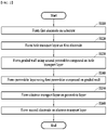
- FIG. 2 is a flowchart illustrating a method of fabricating a perovskite photoelectric device according to an embodiment of the present invention.
- the method of fabricating a perovskite photoelectric device may include a step S110 of forming a first electrode on a substrate, a step S120 of forming a hole transport layer on the first electrode, a step S130 of forming a graded wall using a second perovskite compound on the hole transport layer, a step S140 of forming a perovskite layer using a first perovskite compound on the graded wall, a step S150 of forming an electron transport layer on the perovskite layer, and a step S160 of forming a second electrode 160 on the electron transport layer.
- the graded wall may be formed by applying a solution including the second perovskite compound onto the hole transport layer.
- steps S130 and S140 may be performed at the same time.
- the perovskite layer on which the graded wall has been formed may be formed on the hole transport layer.
- the solution including the second perovskite compound may be coated on the hole transport layer by spray coating or ultrasonic spray coating, thereby forming the graded wall.
- a solution including the first and second perovskite compounds may be coated on the hole transport layer by spray coating or ultrasonic spray coating.
- the spray coating may be applied to any one point on the hole transport layer for 0.1 to 100,000 seconds.
- the spray coating time is less than 0.1 seconds, it is difficult to a graded wall in the form of a thin film on the hole transport layer due to an insufficient amount of the second perovskite compound.
- the spray coating may be performed while moving a spray nozzle at a speed of 0.001 m/min to 20 m/min.
- a discharge amount of the solution, which includes the second perovskite compound, discharged from a spray nozzle may be 0.001 ml/min to 1000 ml/min.
- the discharge amount is less than 0.001 ml/min, the amount of the solution including the second perovskite compound sprayed from the spray nozzle is small, so that all of the solution is blown off before reaching the substrate or the amount applied is small, and thus, a process time is long.
- the discharge amount exceeds 1000 ml/min, the solution is applied in an excessive amount, so that there is difficulty in drying, and thus, it is difficult to obtain a uniform film.
- the thickness of the graded wall may be changed according to a spray coating time.
- the thickness of the graded wall is thin when the spray coating time is short, and the thickness of the graded wall is thick when the spray coating time is long.
- the thickness of the graded wall may be 0.5 nm to 100,000 nm.
- the thickness is less than 0.5 nm, it is difficult to form the graded wall to a uniform thickness on the entire surface, and when the thickness exceeds 100, 000 nm, there is difficulty in applying to a thin film-type LED and solar cell.
- the graded wall formed on the hole transport layer may suppress the movement of anions included in the perovskite layer.
- the anion concertation at the graded wall is higher than that at the perovskite layer, movement of anions included in the perovskite layer to the hole transport layer may be suppressed due to a difference in anion concentrations.
- the anion concentration at the second perovskite compound included in the graded wall is higher than the anion concentration at the first perovskite compound included in the perovskite layer, movement of anions included in the perovskite layer to the hole transport layer due to a difference in anion concentrations may be suppressed.
- a detailed description thereof has been described above with reference to FIG. 1 , and thus, a redundant description thereof is omitted.
- the graded wall has voids smaller than the size of anions included in the perovskite layer, so that movement of anions included in the perovskite layer to the hole transport layer may be suppressed.
- the graded wall formed by the method of fabricating a perovskite photoelectric device according to an embodiment of the present invention suppress the movement of anions included in the perovskite layer to the hole transport layer, thereby being capable of improving the durability of the perovskite photoelectric device.
- the perovskite photoelectric device fabricated by the method of fabricating a perovskite photoelectric device according to an embodiment of the present invention may have a light emitting lifespan (T 90 , at 100cd/m 2 ) of 2,000 hours to 200,000,000 hours.
- a perovskite photoelectric device according to the present invention was fabricated according the following fabrication example, and then the characteristics and effects of the perovskite photoelectric device were evaluated through the following comparative examples and examples.
- Patterned ITO glass (tin oxide doped with indium, 12 ⁇ ) was purchased from HANALINTECH, and a cleaning solution (Micro-90) was purchased from CnP Science.
- TPBi (2,2',2"-(1,3,5-Benzinetriyl)-tris (1-phenyl-1-H-benzimidazole),> 98.0 %) was purchased from TCI Chemicals.
- PEDOT:PSS poly (3,4-ethylenedioxythiophene)-poly (styrenesulfonate), PH500
- CLEVIOS TM poly(styrenesulfonate)
- Methanol, ethanol and acetone were purchased from SAMCHUN CHEMICALS, and all reagents were used without purification.
- SOCP solution was prepared by mixing PEDOT:PSS and PFI in a ratio of 1 : 11.2, and then adding a small amount of DMSO thereto.
- the SOCP solution was spin-coated on a cleaned ITO glass substrate at 2000 rpm for 60 seconds, followed by heat treatment on a 150°C hot plate for 30 minutes.
- the orange CsPbBr 3 perovskite powder in the solution was recovered by filtration, then dissolved in DMSO, recrystallized from ethanol and dried in a vacuum oven at 60°C for 12 hours.
- a CsPbBr 3 perovskite precursor solution was prepared by completely dissolving a CsPbBr 3 perovskite powder (2 mmol, 1.160 g) in a mixed solution of DMSO (8 mL) and DMF (2 mL) at 60°C.
- a Cs 4 PbBr 6 perovskite precursor solution was prepared by completely dissolving the CsPbBr 3 perovskite powder (0.25 mmol, 0.145 g) and the CsPbBr 3 perovskite powder (0.5 mmol, 0.107 g) in DMSO (10 mL) at 60 °C, and then further adding methanol (1 mL) thereto.
- the perovskite precursor solution was deposited by an ultrasonic spray coating system in the atmosphere.
- An ultrasonic spray nozzle was manufactured by CERATORQ, and the operation frequency thereof was 80 kHz.
- a vortex air deflector was mounted on an ultrasonic spray nozzle to improve the uniformity and applicability of the perovskite layer.
- the perovskite precursor solution was directly supplied through an ultrasonic spray nozzle of a syringe pump (KDS 100, KD Scientific, CsPbBr 3 perovskite precursor solution: 0.7 mL/min, Cs 4 PbBr 6 perovskite precursor solution: 1.0 mL/min).
- N 2 gas As a carrier gas for carrying droplets of the perovskite precursor solution to a substrate, N 2 gas was used.
- the pressure of N 2 gas and the distance between the nozzle and the substrate were respectively set to 7 psi and 50 mm which were constantly maintained in all deposition processes.
- a deposition temperature was 150°C.
- the cleaned ITO glass substrate was treated with argon (Ar) plasma for 1 minute to remove organic residues and to make the surface hydrophilic.
- a hole transport layer was formed by spin-coating a SOCP solution on the ITO glass substrate with a hydrophilic surface and then annealing the same.
- a Cs 4 PbBr 6 graded wall and a CsPbBr 3 perovskite layer were formed on the hole transport layer by an ultrasonic spray coating system.
- an electron transport layer and a second electrode were formed by sequentially depositing 70 nm of TPBi, 1 nm of LiF, and 60 nm of Al by a high vacuum thermal evaporator at ⁇ 10 -6 Torr.
- deposition rates thereof were respectively 0.5, 0.1 and 2 ⁇ /s (Angstroms per second).
- An active region was fixed to 0.16 cm 2 , and all devices were encapsulated prior to measurement in an N 2 atmosphere.
- a Cs 4 PbBr 6 perovskite precursor solution was spray-coated on a hole transport layer for 10 seconds to form a graded wall, and then a perovskite layer was formed on the graded wall, thereby fabricating a perovskite photoelectric device.
- a perovskite photoelectric device was fabricated in the same manner as in Example 1, except that a Cs 4 PbBr 6 perovskite precursor solution was spray-coated for 20 seconds.
- a perovskite photoelectric device was fabricated in the same manner as in Example 1, except that a Cs 4 PbBr 6 perovskite precursor solution was spray-coated for 30 seconds.
- a CsPbBr 3 perovskite precursor solution was spray-coated on a hole transport layer, thereby forming a perovskite photoelectric device including a perovskite layer.
- G-wall 10s of Example 1 means that the Cs 4 PbBr 6 perovskite precursor solution was spray-coated for 10 sec to form a graded wall (G-wall)
- G-wall 20s of Example 2 means that the Cs 4 PbBr 6 perovskite precursor solution was spray-coated for 20 sec to form a graded wall (G-wall)
- G-wall 30s of Example 3 means that the Cs 4 PbBr 6 perovskite precursor solution was spray-coated for 30 sec to form a graded wall (G-wall).
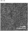
- FIG. 3A illustrates a scanning electron microscope (SEM) image, photographed in a plan view, of a perovskite photoelectric device according to a comparative example of the present invention
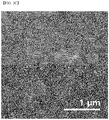
- FIG. 3B illustrates an SEM image, photographed in a plan view, of a perovskite photoelectric device including a graded wall formed thereon according to Example 1 of the present invention
- FIG. 3C illustrates an SEM image, photographed in a plan view, of a perovskite photoelectric device including a graded wall formed thereon according to Example 2 of the present invention
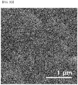
- FIG. 3D illustrates an SEM image, photographed in a plan view, of a perovskite photoelectric device including a graded wall formed thereon according to Example 3 of the present invention.
- the crystal particle size gradually increased with increasing spray coating time with the Cs 4 PbBr 6 perovskite precursor solution is due to repeated crystal particle dissolution and regrowth by balancing the internal and external fluxes of the solvent in the diluted Cs 4 PbBr 6 perovskite precursor solution during the spray coating process.
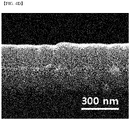
- FIG. 4A illustrates an SEM image of a cross-section of a perovskite photoelectric device according to the comparative example of the present invention
- FIG. 4B illustrates an SEM image of a cross-section of a perovskite photoelectric device including a graded wall formed thereon according to Example 1 of the present invention
- FIG. 4C illustrates an SEM image of a cross-section of a perovskite photoelectric device including a graded wall formed thereon according to Example 2 of the present invention
- FIG. 4D illustrates an SEM image of a cross-section of a perovskite photoelectric device including a graded wall formed thereon according to Example 3 of the present invention.
- the thickness of the graded wall formed on the perovskite layer is not significantly changed regardless of the spray coating time.
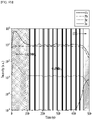
- FIG. 5A is a time-of-flight secondary ion mass spectroscope (TOF-SIMS) graph illustrating a compositional depth profile of a perovskite photoelectric device according to the comparative example of the present invention
- FIG. 5B is a TOF-SIMS graph illustrating a compositional depth profile of a perovskite photoelectric device including a graded wall formed thereon according to Example 1 of the present invention
- FIG. 5C is a TOF-SIMS graph illustrating a compositional depth profile of a perovskite photoelectric device including a graded wall formed thereon according to Example 2 of the present invention
- FIG. 5D is a TOF-SIMS graph illustrating a compositional depth profile of a perovskite photoelectric device including a graded wall formed thereon according to Example 3 of the present invention.
- TOF-SIMS was analyzed by an oxygen ion sputtering beam (1 keV) and a Bi + pulsed primary ion beam (25 keV).
- Cs, Pb, Br and In shown in FIGS. 5A to 5D respectively denote cesium, lead, bromine and tin.
- TOF-SIMS was measured using an oxygen-ion sputtering beam for etching and a Bi + pulsed primary ion beam.
- Examples 1 to 3 show the composition profiles of cesium and bromine around the top surface of the perovskite layer including a graded wall formed thereon, and the constant composition profile of lead.
- the thicknesses of the graded walls of Examples 1 to 3 were respectively -17 nm, -23 nm and -37 nm.
- a mixed region of CsPbBr 3 and Cs 4 PbBr 6 is formed as the graded wall is formed on the perovskite layer, and the thickness of the mixed region increase with increasing spray coating time due to diffusion of Cs 4 PbBr 6 by repeated dissolution and re-growth processes of the perovskite crystal particles.
- the perovskite layer on which a graded wall has been formed is thickly formed as the spray coating time increases to 10 seconds, 20 seconds and 30 seconds.
- FIG. 6 illustrates the XRD patterns of perovskite photoelectric devices according to examples of the present invention and a comparative example.
- CsPbBr 3 denotes the perovskite photoelectric device according to the comparative example
- 10s, 20s and 30s denote the perovskite photoelectric devices according to Examples 1, 2 and 3 in the order.
- the XRD pattern of the perovskite layer according to the comparative example shows that the deposited CsPbBr 3 crystal particle has a cubic shape.
- the Cs 4 PbBr 6 perovskite phase appears as the Cs 4 PbBr 6 perovskite precursor solution is spray-coated for 20 seconds or more.
- Such a result means that the graded wall formed by spray-coating the Cs 4 PbBr 6 perovskite precursor solution for 20 seconds or more is covered by a pure Cs 4 PbBr 6 phase, which is consistent with the TOF-SIMS results of FIGS. 5B to 5D .
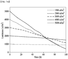
- FIG. 7A illustrates a time dependent-luminance change of a perovskite photoelectric device according to a comparative example of the present invention
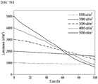
- FIG. 7B illustrates a time dependent-luminance change of a perovskite photoelectric device according to Example 2 of the present invention.
- An acceleration factor may be determined by measuring T time according to light emission intensity. Accordingly, the acceleration factors of the comparative example and Example 2 were respectively determined to be 1.5266 and 1.5400.
- the perovskite light emitting lifespans according to the comparative example and Example 2 were respectively calculated as 3656 hours and 4132 hours by Equation 1.
- the light emitting lifespan increases when the graded wall of the perovskite photoelectric device is formed.
- the compositional depth profile of the perovskite photoelectric device was observed at a luminance of 5000 cd/m 2 or less for 100 hours.
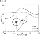
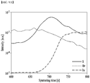
- bromine (Br) moves to the hole transport layer as a bias voltage is applied to the hole transport layer of the comparative example.
- bromine moves to the hole transport layer as a bias voltage is applied to the hole transport layer of Example 2, but a relatively small amount of bromine, compared to the comparative example, moves to the hole transport layer of Example 2.
- Example 2 since the graded wall formed of Cs 4 PbBr 6 having a greater number of monovalent anions than CsPbBr 3 of the perovskite layer is formed in Example 2, the bromine concentration of Example 2 is higher than that of the comparative example, so that a concentration barrier is generated and thus the movement of bromine is relatively less.
- Example 2 wherein the graded wall is formed between the hole transport layer and the perovskite layer, the movement of bromine ions can be efficiently suppressed, so that the light emitting lifespan of the perovskite photoelectric device can be improved and thus the long-term stability thereof can be greatly improved.
Landscapes
- Engineering & Computer Science (AREA)
- Chemical & Material Sciences (AREA)
- Materials Engineering (AREA)
- Physics & Mathematics (AREA)
- Manufacturing & Machinery (AREA)
- Optics & Photonics (AREA)
- Electromagnetism (AREA)
- Photovoltaic Devices (AREA)
- Life Sciences & Earth Sciences (AREA)
- Sustainable Development (AREA)
- Sustainable Energy (AREA)
- Electroluminescent Light Sources (AREA)
Abstract
Description
- This application is a National Stage Entry of PCT International Application No.
PCT/KR2020/010471, which was filed on August 07, 2020 Korean Patent Application No. 10-2019-0096837, filed on August 08, 2019 - The present invention relates a perovskite photoelectric device and a method of fabricating the same.
- A perovskite solar cell uses AMX3 (A is a cation, M is a metal cation, X is an anion)-type cubic diatom perovskite material with good electrical properties as a photoactive layer.
- A perovskite solar cell can be manufactured more easily and inexpensively than a silicon solar cell, and a perovskite solar cell with the world's highest light conversion efficiency (22.7%) close to that of a silicon solar cell (about 25%) has been developed.
- However, an existing perovskite light emitting device has a problem in that the light conversion efficiency of a battery rapidly decreases when used for more than 1000 hours.
- This was found to be due to iodine ions, which constitute a photoactive layer of a perovskite light-emitting device, accumulated at an interface under an electrode (team led by Professor Changhee Lee of Electrical and Computer Engineering Department in Seoul National University,).
- To solve this durability problem, research into high-durability PLEDs is underway. However, it is very difficult to develop such PLEDs.
-
Korean Patent Application Publication No. 10-2018-0106851 -
Korean Patent No. 10-1755333 - Therefore, the present invention has been made in view of the above problems, and it is one object of the present invention to provide a perovskite photoelectric device including a hole transport layer, a perovskite layer and a graded wall formed between the hole transport layer and the perovskite layer; and a method of fabricating the perovskite photoelectric device, so that movement of anions in the perovskite layer to other layers can be prevented, and thus, the light emitting lifespan of the perovskite photoelectric device can be improved.
- It is another object of the present invention to provide a perovskite photoelectric device including a hole transport layer, a perovskite layer and a graded wall formed between the hole transport layer and the perovskite layer, wherein an anion concentration at the graded wall is higher than that at the perovskite layer; and a method of fabricating the perovskite photoelectric device, so that the movement of anions of the perovskite compound can be suppressed and thus the durability of the perovskite photoelectric device can be improved.
- It is another object of the present invention to provide a perovskite photoelectric device including a hole transport layer, a perovskite layer and a graded wall formed between the hole transport layer and the perovskite layer; and a method of fabricating the perovskite photoelectric device, wherein the graded wall has voids smaller than the size of anions included in the perovskite layer, so that the movement of anions of the perovskite compound can be suppressed, and thus, the durability of the perovskite photoelectric device can be improved.
- It is yet another object of the present invention to provide a perovskite photoelectric device having longer light emitting lifespan than an existing perovskite photoelectric device at the same luminance and thus having improved durability; and a method of fabricating the perovskite photoelectric device.
- In accordance with an aspect of the present invention, the above and other objects can be accomplished by the provision of a perovskite photoelectric device, including: a first electrode; a hole transport layer formed on the first electrode; a perovskite layer formed on the hole transport layer and made of a first perovskite compound; an electron transport layer formed on the perovskite layer; a second electrode formed on the electron transport layer; and a graded wall formed on the hole transport layer and the perovskite layer and made of a second perovskite compound, wherein the first perovskite compound and the second perovskite compound are represented by Formula 1 below, and the graded wall suppresses movement of anions included in the perovskite layer:
[Formula 1] AaMbXc
where A is a monovalent cation, M is a divalent or trivalent metal cation, X is a monovalent anion, a+2b=c when M is a divalent metal cation, a+3B=c when M is a trivalent metal cation, and a, b and c are natural numbers. - In accordance with the perovskite photoelectric device according to an embodiment of the present invention, an anion concentration at the graded wall may be higher than an anion concentration at the perovskite layer so that movement of anions included in the perovskite layer is suppressed.
- In accordance with the perovskite photoelectric device according to an embodiment of the present invention, a size of voids of the graded wall may be smaller than a size of anions included in the perovskite layer so that movement of anions included in the perovskite layer is suppressed.
- In accordance with the perovskite photoelectric device according to an embodiment of the present invention, the graded wall may further include at least one of inorganic thin films including a metal chalcogen compound, a metal oxide, a metal halide, and a metal thin film and organic thin films including a graphene thin film, a polymer thin film, a crosslinked polymer thin film, and a monomolecular thin film.
- In accordance with the perovskite photoelectric device according to an embodiment of the present invention, the graded wall may have a thickness of 0.5 nm to 100 µm.
- In accordance with the perovskite photoelectric device according to an embodiment of the present invention, the perovskite photoelectric device may have a light emitting lifespan (T90, at 100 cd/m2) of 2,000 hours to 200,000,000 hours.
- In accordance with another aspect of the present invention, there is provided a method of fabricating a perovskite photoelectric device, the method including: forming a first electrode on a substrate; forming a hole transport layer on the first electrode; forming a graded wall made of a second perovskite compound on the hole transport layer; forming a perovskite layer made of a first perovskite compound on the graded wall; forming an electron transport layer on the perovskite layer; and forming a second electrode on the electron transport layer, wherein the first perovskite compound and the second perovskite compound are represented by Formula 1 below, and the graded wall suppresses movement of anions included in the perovskite layer:
[Formula 1] AaMbXc
where A is a monovalent cation, M is a divalent or trivalent metal cation, X is a monovalent anion, a+2b=c when M is a divalent metal cation, a+3B=c when M is a trivalent metal cation, and a, b and c are natural numbers. - In accordance with the method of fabricating a perovskite photoelectric device according to an embodiment of the present invention, the graded wall may be formed by spray-coating the second perovskite compound on the hole transport layer.
- In accordance with the method of fabricating a perovskite photoelectric device according to an embodiment of the present invention, the spray coating may be performed for 0.1 seconds to 100,000 seconds.
- In accordance with the method of fabricating a perovskite photoelectric device according to an embodiment of the present invention, a thickness of the graded wall may be adjusted according to a time for which the spray coating is performed.
- In accordance with the method of fabricating a perovskite photoelectric device according to an embodiment of the present invention, the graded wall may have a thickness of 0.5 nm to 100 µm.
- According to an embodiment of the present invention, the movement of anions in a perovskite layer to other layers can be prevented by forming a graded wall between a hole transport layer and the perovskite layer, so that the light emitting lifespan of a perovskite photoelectric device can be improved.
- According to an embodiment of the present invention, the movement of anions of the perovskite compound can be suppressed by forming a graded wall between a hole transport layer and a perovskite layer, wherein an anion concentration at the graded wall is higher than that at the perovskite layer, so that the durability of the perovskite photoelectric device can be improved.
- According to an embodiment of the present invention, the movement of anions of the perovskite compound can be suppressed by forming a graded wall with voids between a hole transport layer and a perovskite layer, wherein the voids are smaller than the size of anions included in the perovskite layer, so that the durability of the perovskite photoelectric device can be improved.
- According to an embodiment of the present invention, the perovskite photoelectric device has longer light emitting lifespan than an existing perovskite photoelectric device at the same luminance, thus having improved durability.
-
-
FIG. 1 is a sectional view illustrating the structure of a perovskite photoelectric device according to an embodiment of the present invention. -
FIG. 2 is a flowchart illustrating a method of fabricating a perovskite photoelectric device according to an embodiment of the present invention. -
FIG. 3A illustrates a scanning electron microscope (SEM) image, photographed in a plan view, of a perovskite photoelectric device according to a comparative example of the present invention. -
FIG. 3B illustrates an SEM image, photographed in a plan view, of a perovskite photoelectric device including a graded wall formed thereon according to Example 1 of the present invention. -
FIG. 3C illustrates an SEM image, photographed in a plan view, of a perovskite photoelectric device including a graded wall formed thereon according to Example 2 of the present invention. -
FIG. 3D illustrates an SEM image, photographed in a plan view, of a perovskite photoelectric device including a graded wall formed thereon according to Example 3 of the present invention. -
FIG. 4A illustrates an SEM image of a cross-section of a perovskite photoelectric device according to the comparative example of the present invention. -
FIG. 4B illustrates an SEM image of a cross-section of a perovskite photoelectric device including a graded wall formed thereon according to Example 1 of the present invention. -
FIG. 4C illustrates an SEM image of a cross-section of a perovskite photoelectric device including a graded wall formed thereon according to Example 2 of the present invention. -
FIG. 4D illustrates an SEM image of a cross-section of a perovskite photoelectric device including a graded wall formed thereon according to Example 3 of the present invention. -
FIG. 5A is a time-of-flight secondary ion mass spectroscope (TOF-SIMS) graph illustrating a compositional depth profile of a perovskite photoelectric device according to the comparative example of the present invention. -
FIG. 5B is a TOF-SIMS graph illustrating a compositional depth profile of a perovskite photoelectric device including a graded wall formed thereon according to Example 1 of the present invention. -
FIG. 5C is a TOF-SIMS graph illustrating a compositional depth profile of a perovskite photoelectric device including a graded wall formed thereon according to Example 2 of the present invention. -
FIG. 5D is a TOF-SIMS graph illustrating a compositional depth profile of a perovskite photoelectric device including a graded wall formed thereon according to Example 3 of the present invention. -
FIG. 6 illustrates the XRD patterns of perovskite photoelectric devices according to examples of the present invention and a comparative example. -
FIG. 7A illustrates a time dependent-luminance change of a perovskite photoelectric device according to a comparative example of the present invention. -
FIG. 7B illustrates a time dependent-luminance change of a perovskite photoelectric device according to Example 2 of the present invention. -
FIG. 8A is a TOF-SIMS graph illustrating a compositional depth profile according to a sputtering time for an initial state (t=0h) of a perovskite photoelectric device according to a comparative example of the present invention. -
FIG. 8B is a TOF-SIMS graph illustrating a compositional depth profile according to a sputtering time for a final state (t=100h) of the perovskite photoelectric device according to the comparative example of the present invention. -
FIG. 9A is a TOF-SIMS graph illustrating a compositional depth profile according to a sputtering time for an initial state (t=0h) of a perovskite photoelectric device according to Example 2 of the present invention. -
FIG. 9B is a TOF-SIMS graph illustrating a compositional depth profile according to a sputtering time for a final state (t=100h) of the perovskite photoelectric device according to Example 2 of the present invention. - The present invention will now be described more fully with reference to the accompanying drawings and contents disclosed in the drawings. However, the present invention should not be construed as limited to the exemplary embodiments described herein.
- The terms used in the present specification are used to explain a specific exemplary embodiment and not to limit the present inventive concept. Thus, the expression of singularity in the present specification includes the expression of plurality unless clearly specified otherwise in context.
- It will be further understood that the terms "comprise" and/or "comprising", when used in this specification, specify the presence of stated steps, but do not preclude the presence or addition of one or more other steps thereof.
- It should not be understood that arbitrary aspects or designs disclosed in "embodiments", "examples", "aspects", etc. used in the specification are more satisfactory or advantageous than other aspects or designs.
- In addition, the expression "or" means "inclusive or" rather than "exclusive or". That is, unless otherwise mentioned or clearly inferred from context, the expression "x uses a or b" means any one of natural inclusive permutations.
- In addition, as used in the description of the invention and the appended claims, the singular forms "a", "an" and "the" are intended to include the plural forms as well, unless context clearly indicates otherwise.
- Although terms used in the specification are selected from terms generally used in related technical fields, other terms may be used according to technical development and/or due to change, practices, priorities of technicians, etc.
- Therefore, it should not be understood that terms used below limit the technical spirit of the present invention, and it should be understood that the terms are exemplified to describe embodiments of the present invention.
- Also, some of the terms used herein may be arbitrarily chosen by the present applicant. In this case, these terms are defined in detail below. Accordingly, the specific terms used herein should be understood based on the unique meanings thereof and the whole context of the present invention.
- Unless otherwise defined, all terms (including technical and scientific terms) used herein have the same meaning as commonly understood by one of ordinary skill in the art. It will be further understood that terms, such as those defined in commonly used dictionaries, should be interpreted as having a meaning that is consistent with their meaning in the context of the relevant art and the present invention, and will not be interpreted in an idealized or overly formal sense unless expressly so defined herein.
- Meanwhile, in the following description of the present invention, a detailed description of known functions and configurations incorporated herein will be omitted when it may make the subject matter of the present invention unclear.
- The terms used in the specification are defined in consideration of functions used in the present invention, and can be changed according to the intent or conventionally used methods of clients, operators, and users. Accordingly, definitions of the terms should be understood on the basis of the entire description of the present specification.
-
FIG. 1 is a sectional view illustrating the structure of a perovskite photoelectric device according to an embodiment of the present invention. - Referring to
FIG. 1 , a perovskitephotoelectric device 100 according to an embodiment of the present invention includes a substrate (not shown), afirst electrode 110, ahole transport layer 120 formed on thefirst electrode 110, aperovskite layer 140 formed on thehole transport layer 120 and made of a first perovskite compound, anelectron transport layer 150 formed on theperovskite layer 140, asecond electrode 160 formed on theelectron transport layer 150, and a gradedwall 130 formed between thehole transport layer 120 and theperovskite layer 140 and made of a second perovskite compound. - As the substrate, an inorganic material substrate or an organic material substrate may be used.
- The inorganic material substrate may be made of, without being limited to glass, quartz, Al2O3, SiC, Si, GaAs or InP.
- The organic material substrate may be selected from, without being limited to, Kepton foil, polyimide (PI), polyethersulfone (PES), polyacrylate (PAR), polyetherimide (PEI), polyethylene naphthalate (PEN), polyethylene terephthalate (PET), polyphenylene sulfide (PPS), polyarylate, polycarbonate (PC), cellulose triacetate (CTA) and cellulose acetate propionate (CAP).
- The inorganic material substrate and the organic material substrate are more preferably made of a transparent material through which light is transmitted, and any substrate that can be placed on a front electrode may be used. When an organic material substrate is applied, the flexibility of an electrode may be improved.
- The
first electrode 110 is preferably a conductive electrode placed on a substrate and, particularly, a transparent conductive electrode being capable of improving light transmission. For example, thefirst electrode 110 may be a front electrode provided on a light-receiving side an electrode. - For example, the
first electrode 110 may be selected from, without being limited to, the group consisting of fluorine doped tin oxide (FTO), indium doped tin oxide (ITO), Al-doped zinc oxide (AZO), indium doped zinc oxide (IZO) or a mixture thereof. - Preferably, the
first electrode 110 may include ITO, as a transparent electrode with a large work function, so as to facilitate injection of holes into a highest occupied molecular orbital (HOMO) level of theperovskite layer 140. - The
first electrode 110 may be formed on the substrate by thermal evaporation, e-beam evaporation, radio frequency (RF) sputtering, magnetron sputtering, vacuum deposition, chemical vapor deposition, or the like. - In addition, the
first electrode 110 may include a transparent conductive electrode having an OMO (O = organic material or metal oxide, M = metal) structure. - According to an embodiment, the
first electrode 110 may have a sheet resistance of 1 Ω/cm2 to 1000 Ω/cm2 and a transmittance of 80 % to 99.9 %. - When the sheet resistance of the
first electrode 110 is less than 1 Ω/cm2, the transmittance is decreased, and thus, it is difficult to use as a transparent electrode. When the sheet resistance of thefirst electrode 110 is greater than 1000 Ω/cm2, the performance of an element is decreased due to the high sheet resistance. - In addition, when the transmittance of the
first electrode 110 is less than 80%, light extraction or light transmission is low, and thus, the performance of an element is decreased. When the transmittance of thefirst electrode 110 is greater than 99.9%, the performance of an element is decreased due to the high sheet resistance. - As shown in FIG. 1a, the
hole transport layer 120 may be disposed between thefirst electrode 110 and theperovskite layer 140. - According to an embodiment, the
hole transport layer 120 may be disposed between thefirst electrode 110 and the gradedwall 130, as shown in FIG. 1b. - According to an embodiment, the
hole transport layer 120 may serve to move holes injected from thefirst electrode 110 to theperovskite layer 140 when the perovskitephotoelectric device 100 according to an embodiment of the present invention is used as a light emitting device, and may allow holes generated in theperovskite layer 140 to be easily transferred to thefirst electrode 110 when the perovskitephotoelectric device 100 according to an embodiment of the present invention is used a solar cell. - The hole transport layer 120 may be at least one selected from, without being limited to, P3HT (poly[3-hexylthiophene]), MDMO-PPV (poly[2-methoxy-5-(3',7'-dimethyloctyloxyl)]-1,4-phenylene vinylene), MEH-PPV (poly[2-methoxy-5-(2"-ethylhexyloxy)-p-phenylene vinylene]), P3OT (poly (3-octyl thiophene)), POT ( poly (octyl thiophene)), P3DT (poly (3-decyl thiophene)), P3DDT (poly (3-dodecyl thiophene), PPV (poly (p-phenylene vinylene)), TFB (poly (9,9'-dioctylfluorene-co-N-(4-butylphenyl)diphenyl amine), Polyaniline, Spiro-MeOTAD ([2,22',7,77'-tetrkis (N,N-dipmethoxyphenylamine)-9,9,9'-spirobi fluorine]), CuSCN, CuI, MoOx, VOx, NiOx, CuOx, PCPDTBT (Poly[2,1,3-benzothiadiazole-4,7-diyl[4,4-bis(2-ethylhexyl-4H- cyclopenta [2,1-b:3,4-b']dithiophene-2,6-diyl]], Si-PCPDTBT (poly[ (4,4'-bis(2-ethylhexyl)dithieno[3,2-b:2',3'-d]silole)-2,6-diyl-alt-(2,1,3-benzothiadiazole)-4,7-diyl]), PBDTTPD (poly ( (4,8-diethylhexyloxyl) benzo ([1,2-b:4,5-b']dithiophene)-2,6-diyl)-alt-( (5-octylthieno[3,4-c]pyrrole-4,6-dione)-1,3-diyl)), PFDTBT (poly[2,7-(9-(2-ethylhexyl)-9-hexyl-fluorene)-alt-5,5-(4', 7,-di-2-thienyl-2',1', 3'-benzothiadiazole)]), PFO-DBT (poly[2,7-.9,9-(dioctyl-fluorene)-alt-5,5-(4',7'-di-2-.thienyl-2', 1', 3'-benzothiadiazole)]), PSiFDTBT (poly[ (2,7-dioctylsilafluorene)-2,7-diyl-alt-(4,7-bis(2-thienyl)-2,1,3-benzothiadiazole)-5,5'-diyl]), PSBTBT (poly[ (4,4'-bis(2-ethylhexyl)dithieno[3,2-b:2',3'-d]silole)-2,6-diyl-alt-(2,1,3-benzothiadiazole)-4,7-diyl]), PCDTBT (Poly [[9-(1-octylnonyl)-9H-carbazole-2,7-diyl]-2,5-thiophenediyl-2,1,3-benzothiadiazole-4,7-diyl-2,5-thiophenediyl]), PFB (poly (9,9'-dioctylfluorene-co-bis(N,N'-(4,butylphenyl))bis(N,N'-phenyl-1,4-phenylene)diamine), F8BT (poly (9,9'-dioctylfluorene-cobenzothiadiazole), PEDOT (poly (3,4-ethylenedioxythiophene)), PEDOT:PSS, poly (3,4-ethylenedioxythiophene) poly (styrenesulfonate), PTAA (poly (triarylamine)), poly (4-butylphenyldiphenyl-amine), 4,4'-bis[N-(1-naphtyl)-N-phenylamino]-biphenyl (NPD), PEDOT:PSSbis(N-(1-naphthyl-n-phenyl))benzidine (α-NPD) mixed with PFI (perfluorinated ionomer), N,N'-di (naphthalen-1-yl)-N,N'-diphenyl-benzidine (NPB), N,N'-diphenyl-N,N'-bis(3-methylphenyl)-1,1'-diphenyl-4,4'-diamine (TPD), copper phthalocyanine (CuPc), 4,4',4"-tris (3-methylphenylamino)triphenylamine (m-MTDATA), 4,4',4"-tris (3-methylphenylamino)phenoxybenzene (m-MTDAPB), starburst-type amines4,4',4"-tri (N-carbazolyl)triphenylamine (TCTA), 4,4',4"-tris (N-(2-naphthyl)-N-phenylamino)-triphenylamine (2-TNATA) and a copolymer thereof.

- The
perovskite layer 140 may be formed between thehole transport layer 120 and theelectron transport layer 150. - The first perovskite compound forming the
perovskite layer 140 may be represented byFormula 1 below:
[Formula 1] AaMbXc
whereFormula 1, A is a monovalent cation, M is a divalent or trivalent metal cation, X is a monovalent anion, a+2b=c when M is a divalent metal cation, a+3B=c when M is a trivalent metal cation, and a, b and c are natural numbers. - Particularly, A may be a monovalent organic cation, a monovalent inorganic cation or a combination thereof.
- The perovskite compound may an organic/inorganic hybrid perovskite compound or an inorganic metal halide perovskite compound, depending upon the type of A of
Formula 1. - More particularly, when A in
Formula 1 is a monovalent organic cation, the perovskite compound may be composed of an organic material A and inorganic materials M and X, and thus, may be an organic/inorganic hybrid perovskite compound composed of an organic material and an inorganic material. - On the other hand, when A in
Formula 1 is a monovalent inorganic cation, the perovskite compound may be composed of inorganic materials A, M and X, and thus, may be an inorganic metal halide perovskite compound composed of only an inorganic material. - When the monovalent cation A is an organic cation, it may be a C1~24 linear or branched alkyl group, an amine group (-NH3), a hydroxyl group (-OH), a cyano group (-CN), a halogen group, a nitro group (-NO), a methoxy group (-OCH3) or an imidazolium group-substituted C1~24 linear or branched alkyl group or a combination thereof.
- When the monovalent cation A is an inorganic cation, it may be Li+, Na+, K+, Rb+, Cs+, Fr+, Cu (I)+, Ag (I)+, Au (I)+ or a combination thereof.
- The divalent metal cation may include at least one of Pb2+, Sn2+, Ge2+, Cu2+, Co2+, Ni2+, Ti2+, Zr2+, Hf2+, Rf2+, In3+, Bi3+, Co3+, Sb3+ and Ni3+.
- According to an embodiment, when M of
Formula 1 is a trivalent metal cation, it may be In3+, Bi3+, Co3+, Sb3+, Ni3+, Al3+, Ga3+, Tl3+, Sc3+, Y3+, La3+, Ce3+, Fe3+, Ru3+, Cr3+, V3+, Ti3+ or a combination thereof. - Particularly, when M is the divalent metal cation, a+2b=c and, when M is a trivalent cation, a+3B=c.
- X, which is a monovalent anion, may include F-, Cl-, Br-, I-, BF4 -, PF6 - and SCN-, and is not limited thereto unless the ion size is excessively large.
- According to an embodiment, the first perovskite compound may have a single structure, a double structure, a triple structure, or a Ruddlesden-Popper structure.
- A perovskite compound having a single structure corresponds to the perovskite of
Formula 1 having a three-dimensional single phase, and a perovskite compound having a double structure corresponds to theperovskite layer 140 formed by alternately stacking (A1)a (M1)b (X1)c and (A2)a (M2)b (X2)c. - Here, in Formulas (A1)a(M1)b(X1)c and (A2)a (M2)b (X2)c, A1 and A2 are the same or different monovalent cations, M1 and M2 are the same or different divalent metal cations or trivalent metal cations, and X1 and X2 are the same or different monovalent anions. Here, at least one of A1, M1 and X1 differs from A2, M2 and X2.
- The perovskite compound having a triple structure is a perovskite film formed by alternately stacking (A1)a (M1)b (X1)c, (A2)a (M2)b(X2)c and (A3)a (M3)b (X3)c. Here, A1, A2 and A3 are the same or different monovalent cations, M1, M2 and M3 are the same or different divalent metal cations or trivalent metal cations, and X1, X2 and X3 are the same or different monovalent anions. Here, A1, M1 and X1, and A2, M2 and X2, and A3, M3 and X3 differ from each other by at least one.
- The Ruddlesden-Popper structure is (A1)a (M1)b (X1)c{ (A2)a (M2)b (X2)c}n (A1)a (M1)b (X1)c. Here, n is a natural number.
- The
electron transport layer 150 may be placed between theperovskite layer 140 and thesecond electrode 160. - When the perovskite
photoelectric device 100 according to an embodiment of the present invention is used as a light emitting device, theelectron transport layer 150 may move electrons injected from thesecond electrode 160 to theperovskite layer 140, and when the perovskitephotoelectric device 100 according to an embodiment of the present invention is used as a solar cell, theelectron transport layer 150 may allow electrons generated in theperovskite layer 140 to be easily transferred to thesecond electrode 160. - The electron transport layer 150 may include, without being limited to, at least one of fullerene (C60), a fullerene derivative, perylene, TPBi (2,2',2"-(1,3,5-benzinetriyl)-tris (1-phenyl-1-H-benzimidazole)), PBI (polybenzimidazole) and PTCBI (3,4,9,10-perylene-tetracarboxylic bis-benzimidazole), NDI (Naphthalene diimide) and a derivative thereof, TiO2, SnO2, ZnO, ZnSnO3, 2,4,6-Tris (3-(pyrimidin-5-yl)phenyl)-1,3,5-triazine, 8-Hydroxyquinolinolato-lithium, 1,3,5-Tris (1-phenyl-1Hbenzimidazol- 2-yl)benzene, 6,6'-Bis[5-(biphenyl-4-yl)-1,3,4-oxadiazo-2-yl]-2,2'-bipyridyl, 4,4'-Bis (4,6-diphenyl-1,3,5-triazin-2-yl)biphenyl (BTB), Rb2CO3 (Rubidium carbonate) and ReO3 (Rhenium (VI) oxide), and the fullerene derivative may be, without being limited to, PCBM ( (6,6)-phenyl-C61-butyric acid-methylester) or PCBCR ( (6,6)-phenyl-C61-butyric acid cholesteryl ester).
- However, in an inverted structure, the
electron transport layer 150 may be mainly made of, without being limited to a TiO2-based or Al2O3-based porous material. - The
second electrode 160 may be a commonly used rear electrode. Particularly, thesecond electrode 160 may be, without being limited to, lithium fluoride/aluminum (LiF/Al), gold (Au), silver (Ag), platinum (Pt), palladium (Pd), copper (Cu), aluminum (Al), carbon (C), cobalt sulfide (CoS), copper sulfide (CuS), nickel oxide (NiO) or a mixture thereof. Thesecond electrode 160 may also be formed by the method described regarding thefirst electrode 110, and thus, a redundant description thereof is omitted. - As the
second electrode 160, a metal-based electrode having a low large work function to facilitate injection of electrons into the highest occupied molecular orbital (HOMO) level of theperovskite layer 140 and having excellent internal reflectance may be used. - The graded
wall 130 may be formed between thehole transport layer 120 and theperovskite layer 140. - The second perovskite compound constituting the graded
wall 130 is represented byFormula 1 and may inhibit the movement of anions included in the first perovskite compound constituting theperovskite layer 140. - According an existing perovskite light-emitting device, the anions included in the photoactive layer made of the perovskite compound move toward a positive electrode due to electrostatic properties thereof and are accumulated at the electrode interface.
- As such, anions move toward an electrode (especially positive electrode) and move to the hole transport layer formed on the positive electrode, which causes the lifespan of the perovskite light-emitting device to decrease.
- Accordingly, to prevent anions included in the
perovskite layer 140 from moving to thehole transport layer 120, the gradedwall 130 may be formed between thehole transport layer 120 and theperovskite layer 140. - According to an embodiment, since an anion concentration at the graded
wall 130 is higher than that at theperovskite layer 140, movement of the anions included in theperovskite layer 140 to thehole transport layer 120 may be inhibited due to a difference in the anion concentrations. - Particularly, when the type of anions of the second perovskite compound is the same as that of the first perovskite compound and the number of anions of the second perovskite compound is larger than that of the first perovskite compound, the concentration of anions included in the
perovskite layer 140 may be smaller than that included in the graded wall. - Due to such an anion concentration difference, anions included in in the
perovskite layer1 140 are not moved to thehole transport layer 120 by the gradedwall 130. - For example, when the first perovskite compound is CsPbBr3 (AMX3 structure as a mixture of AX and MX2), the content of anions (X) in the second perovskite compound may increase because AX or MX2 is further added to the first perovskite compound.
- Particularly, when n=1 and Cs2PbBr4, n=3 in CsPbBr3+nCsBr=Cs (1+n)PbBr (3+n), the second perovskite compound may be Cs4PbBr6, or the like.
- Alternatively, the formula of the second perovskite compound may be obtained using nCsPbBr3+mPbBr2=CsnPb (n+m)Br (3n+2m) (where n= integer of 0 or more, and m an integer of 1 or more).
- According to an embodiment, the graded
wall 130 has voids smaller than the size of anions included in theperovskite layer 140, so that the movement of anions included in theperovskite layer 140 to thehole transport layer 120 may be suppressed. - That is, since the graded
wall 130 has voids smaller than the size of anions included in theperovskite layer 140, anions included in theperovskite layer 140 do not pass through voids of the gradedwall 130, so that movement of the anions to thehole transport layer 120 may be suppressed. - To have voids smaller than the size of anions included in the
perovskite layer 140, the gradedwall 130 may further include at least one of inorganic thin films including a metal chalcogen compound, a metal oxide, a metal halide, and a metal thin film and organic thin films including a graphene thin film, a polymer thin film, a crosslinked polymer thin film, and a monomolecular thin film. - According to an embodiment, at least one of the cation (A), metal cation (M), and anion (X) of the first perovskite compound may be the same as or different from at least one of the cation (A), metal cation (M), and anion (X) of the second perovskite compound.
- For example, the first perovskite compound may be CsPbBr3, and the second perovskite compound may be Cs4PbBr6, without being limited thereto.
- The second perovskite compound has the same characteristics as those of the first perovskite compound except that the number of anions in the second perovskite compound is greater than that of the first perovskite compound, and thus, a redundant description thereof is omitted.
- Accordingly, since in the case of the perovskite
photoelectric device 100 according to an embodiment of the present invention, the gradedwall 130 is formed between thehole transport layer 120 and theperovskite layer 140, movement of anions of the perovskite compound to thehole transport layer 120 may be suppressed, so that the light emitting lifespan of the perovskitephotoelectric device 100 may be improved. - Hereinafter, a method of fabricating the perovskite
photoelectric device 100 according to an embodiment of the present invention is described with reference toFIG. 2 and the perovskitephotoelectric device 100 according to an embodiment of the present invention is also more particularly described. -
FIG. 2 is a flowchart illustrating a method of fabricating a perovskite photoelectric device according to an embodiment of the present invention. - Referring to
FIG. 2 , the method of fabricating a perovskite photoelectric device according to an embodiment of the present invention may include a step S110 of forming a first electrode on a substrate, a step S120 of forming a hole transport layer on the first electrode, a step S130 of forming a graded wall using a second perovskite compound on the hole transport layer, a step S140 of forming a perovskite layer using a first perovskite compound on the graded wall, a step S150 of forming an electron transport layer on the perovskite layer, and a step S160 of forming asecond electrode 160 on the electron transport layer. - In step S130, the graded wall may be formed by applying a solution including the second perovskite compound onto the hole transport layer.
- According to an embodiment, steps S130 and S140 may be performed at the same time.
- That is, after step S120, the perovskite layer on which the graded wall has been formed may be formed on the hole transport layer.
- According to an embodiment, in step S130, the solution including the second perovskite compound may be coated on the hole transport layer by spray coating or ultrasonic spray coating, thereby forming the graded wall.
- According to an embodiment, when steps S130 and S140 are performed at the same time, a solution including the first and second perovskite compounds may be coated on the hole transport layer by spray coating or ultrasonic spray coating.
- According to an embodiment, the spray coating may be applied to any one point on the hole transport layer for 0.1 to 100,000 seconds.
- The spray coating time is less than 0.1 seconds, it is difficult to a graded wall in the form of a thin film on the hole transport layer due to an insufficient amount of the second perovskite compound.
- When the spray coating time exceeds 100,000 seconds, a graded wall is formed in the form of a very thick film, so that there is difficulty in applying to an LED or solar cell requiring a thin film.
- When a large-area graded wall is formed using a spray coating, the spray coating may be performed while moving a spray nozzle at a speed of 0.001 m/min to 20 m/min.
- When the spray nozzle is moved at a speed of less than 0.001 m/min, there is a disadvantage that a process speed is too low and, when the speed exceeds 20 m/min, it is difficult to obtain a uniform inclined wall without pinholes due to an excessively fast moving speed.
- A discharge amount of the solution, which includes the second perovskite compound, discharged from a spray nozzle may be 0.001 ml/min to 1000 ml/min.
- When the discharge amount is less than 0.001 ml/min, the amount of the solution including the second perovskite compound sprayed from the spray nozzle is small, so that all of the solution is blown off before reaching the substrate or the amount applied is small, and thus, a process time is long. When the discharge amount exceeds 1000 ml/min, the solution is applied in an excessive amount, so that there is difficulty in drying, and thus, it is difficult to obtain a uniform film.
- The thickness of the graded wall may be changed according to a spray coating time.
- Particularly, the thickness of the graded wall is thin when the spray coating time is short, and the thickness of the graded wall is thick when the spray coating time is long.
- According to an embodiment, the thickness of the graded wall may be 0.5 nm to 100,000 nm.
- When the thickness is less than 0.5 nm, it is difficult to form the graded wall to a uniform thickness on the entire surface, and when the thickness exceeds 100, 000 nm, there is difficulty in applying to a thin film-type LED and solar cell.
- The graded wall formed on the hole transport layer may suppress the movement of anions included in the perovskite layer.
- Particularly, since the anion concertation at the graded wall is higher than that at the perovskite layer, movement of anions included in the perovskite layer to the hole transport layer may be suppressed due to a difference in anion concentrations.
- In other words, since the anion concentration at the second perovskite compound included in the graded wall is higher than the anion concentration at the first perovskite compound included in the perovskite layer, movement of anions included in the perovskite layer to the hole transport layer due to a difference in anion concentrations may be suppressed. A detailed description thereof has been described above with reference to
FIG. 1 , and thus, a redundant description thereof is omitted. - According to an embodiment, the graded wall has voids smaller than the size of anions included in the perovskite layer, so that movement of anions included in the perovskite layer to the hole transport layer may be suppressed. A detailed description thereof has been described above with reference to
FIG. 1 , and thus, a redundant description thereof is omitted. - Accordingly, the graded wall formed by the method of fabricating a perovskite photoelectric device according to an embodiment of the present invention suppress the movement of anions included in the perovskite layer to the hole transport layer, thereby being capable of improving the durability of the perovskite photoelectric device.
- Accordingly, the perovskite photoelectric device fabricated by the method of fabricating a perovskite photoelectric device according to an embodiment of the present invention may have a light emitting lifespan (T90, at 100cd/m2) of 2,000 hours to 200,000,000 hours.
- Hereinafter, a perovskite photoelectric device according to the present invention was fabricated according the following fabrication example, and then the characteristics and effects of the perovskite photoelectric device were evaluated through the following comparative examples and examples.
- Patterned ITO glass (tin oxide doped with indium, 12Ω) was purchased from HANALINTECH, and a cleaning solution (Micro-90) was purchased from CnP Science.
- Cesium bromide (CsBr, 99.999%), lead bromide (PbBr2, 99.999%), hydrobromic acid (HBr, 48 % by weight), DMSO (dimethylsulfoxide, 99.7%), DMF (N, N- dimethylformamide, 99.8%), PFI (tetrafluoroethylene-perfluoro-3,6dioxa-4-methyl-7-octenesulfonic acid copolymer, 5 % by weight) and lithium fluoride (LiF, 99.995%) were purchased from Sigma-Aldrich.
- TPBi (2,2',2"-(1,3,5-Benzinetriyl)-tris (1-phenyl-1-H-benzimidazole),> 98.0 %) was purchased from TCI Chemicals.
- In addition, PEDOT:PSS (poly (3,4-ethylenedioxythiophene)-poly (styrenesulfonate), PH500) was purchased from CLEVIOS™.
- Methanol, ethanol and acetone were purchased from SAMCHUN CHEMICALS, and all reagents were used without purification.
- SOCP solution was prepared by mixing PEDOT:PSS and PFI in a ratio of 1 : 11.2, and then adding a small amount of DMSO thereto.
- The SOCP solution was spin-coated on a cleaned ITO glass substrate at 2000 rpm for 60 seconds, followed by heat treatment on a 150°C hot plate for 30 minutes.
- First, a PbBr2/HBr solution (3.67 g/8 mL) and CsBr/H2O solution (2.12 g/3 mL) were reacted to prepare a CsPbBr3 perovskite powder.
- The orange CsPbBr3 perovskite powder in the solution was recovered by filtration, then dissolved in DMSO, recrystallized from ethanol and dried in a vacuum oven at 60°C for 12 hours.
- A CsPbBr3 perovskite precursor solution was prepared by completely dissolving a CsPbBr3 perovskite powder (2 mmol, 1.160 g) in a mixed solution of DMSO (8 mL) and DMF (2 mL) at 60°C.
- A Cs4PbBr6 perovskite precursor solution was prepared by completely dissolving the CsPbBr3 perovskite powder (0.25 mmol, 0.145 g) and the CsPbBr3 perovskite powder (0.5 mmol, 0.107 g) in DMSO (10 mL) at 60 °C, and then further adding methanol (1 mL) thereto.
- The perovskite precursor solution was deposited by an ultrasonic spray coating system in the atmosphere.
- An ultrasonic spray nozzle was manufactured by CERATORQ, and the operation frequency thereof was 80 kHz.
- A vortex air deflector was mounted on an ultrasonic spray nozzle to improve the uniformity and applicability of the perovskite layer.
- The perovskite precursor solution was directly supplied through an ultrasonic spray nozzle of a syringe pump (
KDS 100, KD Scientific, CsPbBr3 perovskite precursor solution: 0.7 mL/min, Cs4PbBr6 perovskite precursor solution: 1.0 mL/min). - As a carrier gas for carrying droplets of the perovskite precursor solution to a substrate, N2 gas was used.
- The pressure of N2 gas and the distance between the nozzle and the substrate were respectively set to 7 psi and 50 mm which were constantly maintained in all deposition processes. A deposition temperature was 150°C.
- The patterned ITO glass substrate (ITO substrate = 25 mm × 25 mm, etching area = 10 mm × 25 mm) was sequentially washed with a cleaning solution, deionized water, acetone and ethanol, and then dried with compressed N2 gas.
- The cleaned ITO glass substrate was treated with argon (Ar) plasma for 1 minute to remove organic residues and to make the surface hydrophilic.
- A hole transport layer was formed by spin-coating a SOCP solution on the ITO glass substrate with a hydrophilic surface and then annealing the same.
- A Cs4PbBr6 graded wall and a CsPbBr3 perovskite layer were formed on the hole transport layer by an ultrasonic spray coating system.
- The thicknesses of the perovskite layer and the graded wall were controlled by a spray coating time (CsPbBr3=300 sec, Cs4PbBr6=0, 10, 20 and 30 sec).
- After depositing the perovskite layer and the graded wall, an electron transport layer and a second electrode were formed by sequentially depositing 70 nm of TPBi, 1 nm of LiF, and 60 nm of Al by a high vacuum thermal evaporator at <10-6 Torr. Here, deposition rates thereof were respectively 0.5, 0.1 and 2 Å/s (Angstroms per second).
- An active region was fixed to 0.16 cm2, and all devices were encapsulated prior to measurement in an N2 atmosphere.
- A Cs4PbBr6 perovskite precursor solution was spray-coated on a hole transport layer for 10 seconds to form a graded wall, and then a perovskite layer was formed on the graded wall, thereby fabricating a perovskite photoelectric device.
- A perovskite photoelectric device was fabricated in the same manner as in Example 1, except that a Cs4PbBr6 perovskite precursor solution was spray-coated for 20 seconds.
- A perovskite photoelectric device was fabricated in the same manner as in Example 1, except that a Cs4PbBr6 perovskite precursor solution was spray-coated for 30 seconds.
- A CsPbBr3 perovskite precursor solution was spray-coated on a hole transport layer, thereby forming a perovskite photoelectric device including a perovskite layer.
- The examples and the comparative example were summarized in Table 1 below according to the presence or absence of a graded wall and the spray coating time.
[Table 1] Classification Presence or absence of graded wall Number of graded walls Spray coating time Comparative Example (CsPbBr3) X 0 - Example 1 (G- wall 10s)0 1 10 seconds Example 2 (G-wall 20s) 0 1 20 seconds Example 3 (G-wall 30s) 0 1 30 seconds - Here, G-
wall 10s of Example 1 means that the Cs4PbBr6 perovskite precursor solution was spray-coated for 10 sec to form a graded wall (G-wall), G-wall 20s of Example 2 means that the Cs4PbBr6 perovskite precursor solution was spray-coated for 20 sec to form a graded wall (G-wall), and G-wall 30s of Example 3 means that the Cs4PbBr6 perovskite precursor solution was spray-coated for 30 sec to form a graded wall (G-wall). -
FIG. 3A illustrates a scanning electron microscope (SEM) image, photographed in a plan view, of a perovskite photoelectric device according to a comparative example of the present invention,FIG. 3B illustrates an SEM image, photographed in a plan view, of a perovskite photoelectric device including a graded wall formed thereon according to Example 1 of the present invention,FIG. 3C illustrates an SEM image, photographed in a plan view, of a perovskite photoelectric device including a graded wall formed thereon according to Example 2 of the present invention, andFIG. 3D illustrates an SEM image, photographed in a plan view, of a perovskite photoelectric device including a graded wall formed thereon according to Example 3 of the present invention. - Referring to
FIGS. 3A to 3D , it can be confirmed that the diameter of crystal grains on an upper surface gradually increases as the spray coating time with the Cs4PbBr6 perovskite precursor solution increases. - The crystal particle size gradually increased with increasing spray coating time with the Cs4PbBr6 perovskite precursor solution is due to repeated crystal particle dissolution and regrowth by balancing the internal and external fluxes of the solvent in the diluted Cs4PbBr6 perovskite precursor solution during the spray coating process.
-
FIG. 4A illustrates an SEM image of a cross-section of a perovskite photoelectric device according to the comparative example of the present invention,FIG. 4B illustrates an SEM image of a cross-section of a perovskite photoelectric device including a graded wall formed thereon according to Example 1 of the present invention,FIG. 4C illustrates an SEM image of a cross-section of a perovskite photoelectric device including a graded wall formed thereon according to Example 2 of the present invention, andFIG. 4D illustrates an SEM image of a cross-section of a perovskite photoelectric device including a graded wall formed thereon according to Example 3 of the present invention. - Referring to
FIGS. 4A to 4D , it can be confirmed that the thickness of the graded wall formed on the perovskite layer is not significantly changed regardless of the spray coating time. - This is because a Cs4PbBr6 perovskite precursor solution at a low concentration was used for spray coating.
-
FIG. 5A is a time-of-flight secondary ion mass spectroscope (TOF-SIMS) graph illustrating a compositional depth profile of a perovskite photoelectric device according to the comparative example of the present invention,FIG. 5B is a TOF-SIMS graph illustrating a compositional depth profile of a perovskite photoelectric device including a graded wall formed thereon according to Example 1 of the present invention,FIG. 5C is a TOF-SIMS graph illustrating a compositional depth profile of a perovskite photoelectric device including a graded wall formed thereon according to Example 2 of the present invention, andFIG. 5D is a TOF-SIMS graph illustrating a compositional depth profile of a perovskite photoelectric device including a graded wall formed thereon according to Example 3 of the present invention. - Here, TOF-SIMS was analyzed by an oxygen ion sputtering beam (1 keV) and a Bi+ pulsed primary ion beam (25 keV).
- In addition, Cs, Pb, Br and In shown in
FIGS. 5A to 5D respectively denote cesium, lead, bromine and tin. - Referring to
FIGS. 5A to 5D , to measure the compositional depth profile of the perovskite layer including a graded wall formed thereon according to a spray coating time with the Cs4PbBr6 perovskite precursor solution, TOF-SIMS was measured using an oxygen-ion sputtering beam for etching and a Bi+ pulsed primary ion beam. - As shown in
FIG. 5A , when the compositional depth profile from a top surface of the perovskite layer including a graded wall formed thereon to a bottom surface of the ITO glass substrate was detected, a constant compositional depth profile of cesium (Cs), lead (Pb) and bromine (Br) was shown. - Conversely, it can be confirmed that, as shown in
FIGS. 5B to 5D , Examples 1 to 3 show the composition profiles of cesium and bromine around the top surface of the perovskite layer including a graded wall formed thereon, and the constant composition profile of lead. - Here, the thicknesses of the graded walls of Examples 1 to 3 were respectively -17 nm, -23 nm and -37 nm.
- A mixed region of CsPbBr3 and Cs4PbBr6 is formed as the graded wall is formed on the perovskite layer, and the thickness of the mixed region increase with increasing spray coating time due to diffusion of Cs4PbBr6 by repeated dissolution and re-growth processes of the perovskite crystal particles.
- That is, it can be confirmed that the perovskite layer on which a graded wall has been formed is thickly formed as the spray coating time increases to 10 seconds, 20 seconds and 30 seconds.
-
FIG. 6 illustrates the XRD patterns of perovskite photoelectric devices according to examples of the present invention and a comparative example. - Here, CsPbBr3 denotes the perovskite photoelectric device according to the comparative example, and 10s, 20s and 30s denote the perovskite photoelectric devices according to Examples 1, 2 and 3 in the order.
- Referring to
FIG. 6 , the XRD pattern of the perovskite layer according to the comparative example shows that the deposited CsPbBr3 crystal particle has a cubic shape. - Particularly, referring to the XRD pattern enlarged at 2θ=24~27° of
FIG. 6 , the Cs4PbBr6 perovskite phase appears as the Cs4PbBr6 perovskite precursor solution is spray-coated for 20 seconds or more. - It can be confirmed that the XRD peak at 2θ=24~27° is the same as the XRD pattern of pure Cs4PbBr6 in the existing literature.
- Such a result means that the graded wall formed by spray-coating the Cs4PbBr6 perovskite precursor solution for 20 seconds or more is covered by a pure Cs4PbBr6 phase, which is consistent with the TOF-SIMS results of
FIGS. 5B to 5D . -
FIG. 7A illustrates a time dependent-luminance change of a perovskite photoelectric device according to a comparative example of the present invention, andFIG. 7B illustrates a time dependent-luminance change of a perovskite photoelectric device according to Example 2 of the present invention. - At initial luminance (L0) of 5000cd/m2, 4000cd/m2, 3000cd/m2, 2000cd/m2 and 1000 cd/m2, a change in the luminance of each of the comparative example and Example 2 was observed for 100 hours.
- In addition, the light emitting lifespan (T90, at 100cd/m2) of each of the perovskite photoelectric devices according to the comparative example and Example 2 was calculated through
Equation 1 below:
- An acceleration factor may be determined by measuring T time according to light emission intensity. Accordingly, the acceleration factors of the comparative example and Example 2 were respectively determined to be 1.5266 and 1.5400.
- Accordingly, the perovskite light emitting lifespans according to the comparative example and Example 2 were respectively calculated as 3656 hours and 4132 hours by
Equation 1. - That is, it can be confirmed that the light emitting lifespan increases when the graded wall of the perovskite photoelectric device is formed.
- Hereinafter, to prove the reason for improving durability of the perovskite photoelectric device according to the presence or absence of the graded wall, the compositional depth profile of the perovskite photoelectric device was observed at a luminance of 5000 cd/m2 or less for 100 hours.
-
FIG. 8A is a TOF-SIMS graph illustrating a compositional depth profile according to a sputtering time for an initial state (t=0h) of a perovskite photoelectric device according to a comparative example of the present invention, andFIG. 8B is a TOF-SIMS graph illustrating a compositional depth profile according to a sputtering time for a final state (t=100h) of the perovskite photoelectric device according to the comparative example of the present invention. - Referring to
FIGS. 8A and8B , it can be confirmed that bromine (Br) moves to the hole transport layer as a bias voltage is applied to the hole transport layer of the comparative example. -
FIG. 9A is a TOF-SIMS graph illustrating a compositional depth profile according to a sputtering time for an initial state (t=0h) of a perovskite photoelectric device according to Example 2 of the present invention, andFIG. 9B is a TOF-SIMS graph illustrating a compositional depth profile according to a sputtering time for a final state (t=100h) of the perovskite photoelectric device according to Example 2 of the present invention. - Referring to
FIGS. 9A and9B , it can be confirmed that bromine moves to the hole transport layer as a bias voltage is applied to the hole transport layer of Example 2, but a relatively small amount of bromine, compared to the comparative example, moves to the hole transport layer of Example 2. - It can be seen that, since the graded wall formed of Cs4PbBr6 having a greater number of monovalent anions than CsPbBr3 of the perovskite layer is formed in Example 2, the bromine concentration of Example 2 is higher than that of the comparative example, so that a concentration barrier is generated and thus the movement of bromine is relatively less.
- In conclusion, in the case of Example 2 wherein the graded wall is formed between the hole transport layer and the perovskite layer, the movement of bromine ions can be efficiently suppressed, so that the light emitting lifespan of the perovskite photoelectric device can be improved and thus the long-term stability thereof can be greatly improved.
- Although the present invention has been described through limited examples and figures, the present invention is not intended to be limited to the examples. Those skilled in the art will appreciate that various modifications, additions and substitutions are possible, without departing from the scope and spirit of the invention. Therefore, it should be understood that there is no intent to limit the invention to the embodiments disclosed, rather, the invention is to cover all modifications, equivalents, and alternatives falling within the spirit and scope of the invention as defined by the claims.
-
- 100:
- perovskite photoelectric device
- 110:
- first electrode
- 120:
- hole transport layer
- 130:
- graded wall
- 140:
- perovskite layer
- 150:
- electron transport layer
- 160:
- second electrode
Claims (11)
- A perovskite photoelectric device, comprising:a first electrode;a hole transport layer formed on the first electrode;a perovskite layer formed on the hole transport layer and made of a first perovskite compound;an electron transport layer formed on the perovskite layer;a second electrode formed on the electron transport layer; anda graded wall formed on the hole transport layer and the perovskite layer and made of a second perovskite compound,wherein the first perovskite compound and the second perovskite compound are represented by Formula 1 below, andthe graded wall suppresses movement of anions comprised in the perovskite layer:
[Formula 1] AaMbXc
where A is a monovalent cation, M is a divalent or trivalent metal cation, X is a monovalent anion, a+2b=c when M is a divalent metal cation, a+3B=c when M is a trivalent metal cation, and a, b and c are natural numbers. - The perovskite photoelectric device according to claim 1, wherein an anion concentration at the graded wall is higher than an anion concentration at the perovskite layer so that movement of anions comprised in the perovskite layer is suppressed.
- The perovskite photoelectric device according to claim 1, wherein a size of voids of the graded wall is smaller than a size of anions comprised in the perovskite layer so that movement of anions comprised in the perovskite layer is suppressed.
- The perovskite photoelectric device according to claim 3, wherein the graded wall further comprises at least one of inorganic thin films comprising a metal chalcogen compound, a metal oxide, a metal halide, and a metal thin film and organic thin films comprising a graphene thin film, a polymer thin film, a crosslinked polymer thin film, and a monomolecular thin film.
- The perovskite photoelectric device according to claim 1, wherein the graded wall has a thickness of 0.5 nm to 100 µm.
- The perovskite photoelectric device according to claim 1, wherein the perovskite photoelectric device has a light emitting lifespan (T90, at 100 cd/m2) of 2,000 hours to 200,000,000 hours.
- A method of fabricating a perovskite photoelectric device, the method comprising:forming a first electrode on a substrate;forming a hole transport layer on the first electrode;forming a graded wall made of a second perovskite compound on the hole transport layer;forming a perovskite layer made of a first perovskite compound on the graded wall;forming an electron transport layer on the perovskite layer; andforming a second electrode on the electron transport layer,wherein the first perovskite compound and the second perovskite compound are represented by Formula 1 below, andthe graded wall suppresses movement of anions comprised in the perovskite layer:
[Formula 1] AaMbXc
where A is a monovalent cation, M is a divalent or trivalent metal cation, X is a monovalent anion, a+2b=c when M is a divalent metal cation, a+3B=c when M is a trivalent metal cation, and a, b and c are natural numbers. - The method according to claim 7, wherein the graded wall is formed by spray-coating the second perovskite compound on the hole transport layer.
- The method according to claim 8, wherein the spray coating is performed for 0.1 seconds to 100,000 seconds.
- The method according to claim 8, wherein a thickness of the graded wall is adjusted according to a time for which the spray coating is performed.
- The method according to claim 10, wherein the graded wall has a thickness of 0.5 nm to 100 µm.
Applications Claiming Priority (2)
| Application Number | Priority Date | Filing Date | Title |
|---|---|---|---|
| KR1020190096837A KR102272548B1 (en) | 2019-08-08 | 2019-08-08 | A perovskite photoelectric device and manufacturing method thereof |
| PCT/KR2020/010471 WO2021025519A1 (en) | 2019-08-08 | 2020-08-07 | Perovskite photoelectric element and method for manufacturing same |
Publications (2)
| Publication Number | Publication Date |
|---|---|
| EP3996150A1 true EP3996150A1 (en) | 2022-05-11 |
| EP3996150A4 EP3996150A4 (en) | 2023-08-02 |
Family
ID=74502813
Family Applications (1)
| Application Number | Title | Priority Date | Filing Date |
|---|---|---|---|
| EP20849467.4A Pending EP3996150A4 (en) | 2019-08-08 | 2020-08-07 | PEROVSKITE PHOTOELECTRIC ELEMENT AND METHOD FOR ITS MANUFACTURE |
Country Status (4)
| Country | Link |
|---|---|
| US (1) | US12439769B2 (en) |
| EP (1) | EP3996150A4 (en) |
| KR (1) | KR102272548B1 (en) |
| WO (1) | WO2021025519A1 (en) |
Families Citing this family (5)
| Publication number | Priority date | Publication date | Assignee | Title |
|---|---|---|---|---|
| KR102849586B1 (en) * | 2021-04-08 | 2025-08-25 | 삼성디스플레이 주식회사 | Light emitting device and electronic apparatus comprising same |
| EP4319538B1 (en) * | 2021-11-22 | 2025-11-12 | Contemporary Amperex Technology (Hong Kong) Limited | Preparation method for perovskite thin film, and perovskite thin film and solar cell related thereto |
| US12490576B2 (en) * | 2021-11-26 | 2025-12-02 | Board Of Regents, The University Of Texas System | 3D-0D perovskite light-emitting electrochemical cells |
| CN114235771B (en) * | 2021-12-23 | 2023-10-03 | 重庆大学 | A sensing detection method for detecting heavy metal mercury ions |
| KR102709645B1 (en) * | 2022-08-23 | 2024-09-26 | 고려대학교 산학협력단 | Method for producing a pure phase zero-dimensional perovskite compound and pure phase zero-dimensional perovskite compound particles prepared through the same, perovskite optoelectronic device including the same |
Family Cites Families (11)
| Publication number | Priority date | Publication date | Assignee | Title |
|---|---|---|---|---|
| GB201208793D0 (en) * | 2012-05-18 | 2012-07-04 | Isis Innovation | Optoelectronic device |
| KR101574658B1 (en) | 2014-11-06 | 2015-12-07 | 재단법인대구경북과학기술원 | 3-dimentional solar cell based on Perovskite, and the preparation method thereof |
| JP6829682B2 (en) * | 2014-11-06 | 2021-02-10 | エスエヌ ディスプレイ カンパニー リミテッド | A light emitting layer for a perovskite light emitting element, a method for manufacturing the same, and a perovskite light emitting device using the same. |
| US10593816B2 (en) | 2015-01-08 | 2020-03-17 | Korea Research Institute Of Chemical Technology | Method for manufacturing device comprising inorganic/organic hybrid perovskite compound film and device comprising inorganic/organic hybrid perovskite compound film |
| KR101687491B1 (en) | 2015-07-16 | 2016-12-16 | 한국과학기술원 | Ultrafast formation and transfer of organic and inorganic thin-films utilizing spontaneous spreading effect |
| KR20170028054A (en) * | 2015-09-03 | 2017-03-13 | 울산과학기술원 | High-Performance Perovskite Film, Perovskite Light-Emitting Diodes and Method For Producing The Same |
| KR20170079877A (en) * | 2015-12-31 | 2017-07-10 | 주식회사 동진쎄미켐 | Organic Electronic Device Encapsulation Technologies of Adhesive Film and Manufacturing Method Thereof |
| KR20180074577A (en) | 2016-12-23 | 2018-07-03 | 가부시키가이샤 한도오따이 에네루기 켄큐쇼 | Light-emitting element, light-emitting device, electronic device, display device, and lighting device |
| KR102506443B1 (en) | 2017-03-17 | 2023-03-07 | 삼성전자주식회사 | Photoelectric conversion device including perovskite compound and imaging device including the same |
| EP3682489A4 (en) | 2017-09-15 | 2021-10-20 | Energy Everywhere, Inc. | MANUFACTURE OF STACKED PEROWSKITE STRUCTURES |
| KR101998021B1 (en) * | 2018-03-14 | 2019-07-08 | 군산대학교산학협력단 | Perovskite Solar Cells And The Fabrication Method Of The Same |
-
2019
- 2019-08-08 KR KR1020190096837A patent/KR102272548B1/en active Active
-
2020
- 2020-08-07 EP EP20849467.4A patent/EP3996150A4/en active Pending
- 2020-08-07 US US17/633,247 patent/US12439769B2/en active Active
- 2020-08-07 WO PCT/KR2020/010471 patent/WO2021025519A1/en not_active Ceased
Also Published As
| Publication number | Publication date |
|---|---|
| WO2021025519A1 (en) | 2021-02-11 |
| US12439769B2 (en) | 2025-10-07 |
| KR102272548B1 (en) | 2021-07-05 |
| KR20210017495A (en) | 2021-02-17 |
| US20230225140A1 (en) | 2023-07-13 |
| EP3996150A4 (en) | 2023-08-02 |
Similar Documents
| Publication | Publication Date | Title |
|---|---|---|
| KR101587895B1 (en) | Inverted organic electronic device and method for manufacturing the same | |
| Gong et al. | Diverse applications of MoO 3 for high performance organic photovoltaics: fundamentals, processes and optimization strategies | |
| US12439769B2 (en) | Perovskite photoelectric device and manufacturing method thereof | |
| CN103781845B (en) | Vertical phase separation of semiconducting organic material layers | |
| CN102074657B (en) | Organic light emitting apparatus | |
| US9431621B2 (en) | Metal oxide charge transport material doped with organic molecules | |
| CN103943784B (en) | Organic light emitting apparatus | |
| US9214255B2 (en) | P-doped conjugated polymer electrolyte and an organic electronic device using the same | |
| CN101556988B (en) | An organic optoelectronic device with non-doped gain layer and its preparation method | |
| JP6486737B2 (en) | Photoelectric conversion element | |
| KR101422454B1 (en) | Organic Photoelectic Semiconductor Device and Method for Fabricating the Same | |
| KR20090092114A (en) | Electron injecting layer comprising super acid salt, photovoltaic device including the same and electron injecting layer including the same | |
| US20130061928A1 (en) | Organic solar cell and method of manufacturing the same | |
| CN108183176A (en) | A kind of lamination perovskite light emitting diode and preparation method thereof | |
| JP2015134703A (en) | Composition for forming metal oxide-containing layer, and method for producing electronic device | |
| KR102210595B1 (en) | High efficiency perovskite optoelectric device and manufacturing method by the same | |
| JP6675505B2 (en) | Method for manufacturing photoelectric conversion element | |
| KR102260621B1 (en) | A perovskite photoelectric device and manufacturing method thereof | |
| KR102625989B1 (en) | Novel phenanthroline-based compound, preparation method thereof, and optoelectronic device comprising the same as passivation layer | |
| KR102585825B1 (en) | High durability perovskite photoelectric element and method for manufacturing the same | |
| KR102932878B1 (en) | Method for manufacturing optoelectronic device using post-annealing | |
| JP2017527109A (en) | Organic light emitting device and method of manufacturing the same | |
| KR102267155B1 (en) | Perovskite optoelectronic device including mixed dual sites |
Legal Events
| Date | Code | Title | Description |
|---|---|---|---|
| STAA | Information on the status of an ep patent application or granted ep patent |
Free format text: STATUS: THE INTERNATIONAL PUBLICATION HAS BEEN MADE |
|
| PUAI | Public reference made under article 153(3) epc to a published international application that has entered the european phase |
Free format text: ORIGINAL CODE: 0009012 |
|
| STAA | Information on the status of an ep patent application or granted ep patent |
Free format text: STATUS: REQUEST FOR EXAMINATION WAS MADE |
|
| 17P | Request for examination filed |
Effective date: 20220207 |
|
| AK | Designated contracting states |
Kind code of ref document: A1 Designated state(s): AL AT BE BG CH CY CZ DE DK EE ES FI FR GB GR HR HU IE IS IT LI LT LU LV MC MK MT NL NO PL PT RO RS SE SI SK SM TR |
|
| DAV | Request for validation of the european patent (deleted) | ||
| DAX | Request for extension of the european patent (deleted) | ||
| REG | Reference to a national code |
Ref country code: DE Ref legal event code: R079 Free format text: PREVIOUS MAIN CLASS: H01L0031032000 Ipc: H10K0030400000 |
|
| A4 | Supplementary search report drawn up and despatched |
Effective date: 20230704 |
|
| RIC1 | Information provided on ipc code assigned before grant |
Ipc: H10K 50/11 20230101ALN20230628BHEP Ipc: H01L 31/0392 20060101ALI20230628BHEP Ipc: H01L 31/032 20060101ALI20230628BHEP Ipc: H10K 85/50 20230101ALI20230628BHEP Ipc: H10K 30/40 20230101AFI20230628BHEP |