EP3995840B1 - Device and method for monitoring common mode voltage - Google Patents
Device and method for monitoring common mode voltage Download PDFInfo
- Publication number
- EP3995840B1 EP3995840B1 EP21748242.1A EP21748242A EP3995840B1 EP 3995840 B1 EP3995840 B1 EP 3995840B1 EP 21748242 A EP21748242 A EP 21748242A EP 3995840 B1 EP3995840 B1 EP 3995840B1
- Authority
- EP
- European Patent Office
- Prior art keywords
- voltage
- controller
- comparator
- energy storage
- power
- Prior art date
- Legal status (The legal status is an assumption and is not a legal conclusion. Google has not performed a legal analysis and makes no representation as to the accuracy of the status listed.)
- Active
Links
Images






Classifications
-
- G—PHYSICS
- G01—MEASURING; TESTING
- G01R—MEASURING ELECTRIC VARIABLES; MEASURING MAGNETIC VARIABLES
- G01R19/00—Arrangements for measuring currents or voltages or for indicating presence or sign thereof
- G01R19/165—Indicating that current or voltage is either above or below a predetermined value or within or outside a predetermined range of values
- G01R19/16566—Circuits and arrangements for comparing voltage or current with one or several thresholds and for indicating the result not covered by subgroups G01R19/16504, G01R19/16528, G01R19/16533
- G01R19/16576—Circuits and arrangements for comparing voltage or current with one or several thresholds and for indicating the result not covered by subgroups G01R19/16504, G01R19/16528, G01R19/16533 comparing DC or AC voltage with one threshold
-
- G—PHYSICS
- G01—MEASURING; TESTING
- G01R—MEASURING ELECTRIC VARIABLES; MEASURING MAGNETIC VARIABLES
- G01R19/00—Arrangements for measuring currents or voltages or for indicating presence or sign thereof
- G01R19/25—Arrangements for measuring currents or voltages or for indicating presence or sign thereof using digital measurement techniques
- G01R19/2513—Arrangements for monitoring electric power systems, e.g. power lines or loads; Logging
-
- G—PHYSICS
- G01—MEASURING; TESTING
- G01R—MEASURING ELECTRIC VARIABLES; MEASURING MAGNETIC VARIABLES
- G01R19/00—Arrangements for measuring currents or voltages or for indicating presence or sign thereof
- G01R19/25—Arrangements for measuring currents or voltages or for indicating presence or sign thereof using digital measurement techniques
- G01R19/2503—Arrangements for measuring currents or voltages or for indicating presence or sign thereof using digital measurement techniques for measuring voltage only, e.g. digital volt meters (DVM's)
-
- G—PHYSICS
- G01—MEASURING; TESTING
- G01R—MEASURING ELECTRIC VARIABLES; MEASURING MAGNETIC VARIABLES
- G01R15/00—Details of measuring arrangements of the types provided for in groups G01R17/00 - G01R29/00, G01R33/00 - G01R33/26 or G01R35/00
- G01R15/14—Adaptations providing voltage or current isolation, e.g. for high-voltage or high-current networks
- G01R15/144—Measuring arrangements for voltage not covered by other subgroups of G01R15/14
-
- H—ELECTRICITY
- H01—ELECTRIC ELEMENTS
- H01M—PROCESSES OR MEANS, e.g. BATTERIES, FOR THE DIRECT CONVERSION OF CHEMICAL ENERGY INTO ELECTRICAL ENERGY
- H01M50/00—Constructional details or processes of manufacture of the non-active parts of electrochemical cells other than fuel cells, e.g. hybrid cells
- H01M50/50—Current conducting connections for cells or batteries
- H01M50/569—Constructional details of current conducting connections for detecting conditions inside cells or batteries, e.g. details of voltage sensing terminals
-
- H—ELECTRICITY
- H02—GENERATION; CONVERSION OR DISTRIBUTION OF ELECTRIC POWER
- H02J—ELECTRIC POWER NETWORKS; CIRCUIT ARRANGEMENTS OR SYSTEMS FOR SUPPLYING OR DISTRIBUTING ELECTRIC POWER; SYSTEMS FOR STORING ELECTRIC ENERGY
- H02J7/00—Circuit arrangements for charging or discharging batteries or for supplying loads from batteries
- H02J7/02—Circuit arrangements for charging or discharging batteries or for supplying loads from batteries for charging batteries from AC mains by converters
- H02J7/04—Regulation of charging current or voltage
-
- H—ELECTRICITY
- H02—GENERATION; CONVERSION OR DISTRIBUTION OF ELECTRIC POWER
- H02J—ELECTRIC POWER NETWORKS; CIRCUIT ARRANGEMENTS OR SYSTEMS FOR SUPPLYING OR DISTRIBUTING ELECTRIC POWER; SYSTEMS FOR STORING ELECTRIC ENERGY
- H02J7/00—Circuit arrangements for charging or discharging batteries or for supplying loads from batteries
- H02J7/40—Circuit arrangements for charging or discharging batteries or for supplying loads from batteries characterised by the exchange of charge or discharge related data
-
- H—ELECTRICITY
- H02—GENERATION; CONVERSION OR DISTRIBUTION OF ELECTRIC POWER
- H02J—ELECTRIC POWER NETWORKS; CIRCUIT ARRANGEMENTS OR SYSTEMS FOR SUPPLYING OR DISTRIBUTING ELECTRIC POWER; SYSTEMS FOR STORING ELECTRIC ENERGY
- H02J7/00—Circuit arrangements for charging or discharging batteries or for supplying loads from batteries
- H02J7/80—Circuit arrangements for charging or discharging batteries or for supplying loads from batteries including monitoring or indicating arrangements
-
- G—PHYSICS
- G01—MEASURING; TESTING
- G01R—MEASURING ELECTRIC VARIABLES; MEASURING MAGNETIC VARIABLES
- G01R15/00—Details of measuring arrangements of the types provided for in groups G01R17/00 - G01R29/00, G01R33/00 - G01R33/26 or G01R35/00
- G01R15/04—Voltage dividers
-
- H—ELECTRICITY
- H02—GENERATION; CONVERSION OR DISTRIBUTION OF ELECTRIC POWER
- H02J—ELECTRIC POWER NETWORKS; CIRCUIT ARRANGEMENTS OR SYSTEMS FOR SUPPLYING OR DISTRIBUTING ELECTRIC POWER; SYSTEMS FOR STORING ELECTRIC ENERGY
- H02J2207/00—Details of circuit arrangements for charging or discharging batteries or supplying loads from batteries
- H02J2207/20—Charging or discharging characterised by the power electronics converter
-
- H—ELECTRICITY
- H02—GENERATION; CONVERSION OR DISTRIBUTION OF ELECTRIC POWER
- H02J—ELECTRIC POWER NETWORKS; CIRCUIT ARRANGEMENTS OR SYSTEMS FOR SUPPLYING OR DISTRIBUTING ELECTRIC POWER; SYSTEMS FOR STORING ELECTRIC ENERGY
- H02J3/00—Circuit arrangements for AC mains or AC distribution networks
- H02J3/28—Arrangements for balancing of the load in networks by storage of energy
- H02J3/32—Arrangements for balancing of the load in networks by storage of energy using batteries or super capacitors with converting means
Definitions
- the present invention relates to a device and method for monitoring a common mode voltage.
- the energy storage device is used in the form of a battery rack including a plurality of battery modules connected in series and/or in parallel and a charging and discharging device for charging and discharging the plurality of battery modules.
- the battery module includes battery cells, which are secondary batteries, connected in series and/or in parallel.
- the battery rack includes a rack controller (RBMS; rack battery management system) for controlling the charging and discharging device, and a plurality of module controllers (MBMS; module battery management system) that respectively control the plurality of battery modules.
- RBMS rack battery management system
- MBMS module battery management system
- a power conversion device (PCS; power conversion system) is installed outside the energy storage device for charging and discharging.
- the power conversion device converts AC power of a system into DC power and supplies DC power to the energy storage device, or converts DC power of the energy storage device into AC power and supplies AC power to the system.
- Switching noise occurs in accordance with switching performed during this power conversion. Switching noise is caused on a common mode voltage transmitted in a power line between the power conversion device and the energy storage device, which affects an operation and safety of a battery system such as the energy storage device. Accordingly, it is necessary to accurately monitor the common mode voltage for stable operation of the battery system.
- the present invention has been made to solve the problems described above, and an object thereof is to accurately detect a common mode voltage transmitted in a power line between the power conversion device and the energy storage device.
- a device for monitoring a common mode voltage according to claim 1.
- the comparator may include a plurality of comparators, and at least some of the plurality of comparators may be configured to compare different reference voltages to the output of the voltage divider.
- the comparator may be included in the controller, and may compare a value obtained by converting the output of the voltage divider into a digital value with a digital value corresponding to the reference voltage.
- a terminal portion for communicating with outside of the device, and a power supply portion that generates power based on an input from the terminal portion may be further included.
- an isolator formed between a high voltage circuit portion and a low voltage circuit portion the high voltage circuit portion includes the input end, the voltage divider, the comparator, and the low voltage circuit portion includes the terminal portion and the power supply portion to insulate the high voltage circuit portion from the low voltage circuit portion.
- the isolator may include a power isolator for supplying power from the low voltage circuit portion to the high voltage circuit portion, and a communication isolator for transmitting an input from the terminal portion to the controller.
- the controller may transmit an error signal to outside of the device when an abnormality is detected, by the controller, in the voltage applied to the energy storage device.
- the controller may transmit the error signal to a battery management system of the energy storage device.
- the controller may transmit the error signal to an upper level controller that manages the energy storage device.
- the voltage applied to the input end may be a voltage between the node and a chassis that is the ground of the energy storage device.
- the device and method for monitoring the common mode voltage described above it is possible to accurately detect the common mode voltage transferred in the power line between the conversion device and the energy storage device, thereby enabling stable operation of the battery system.
- first, second, firstly, or secondly may modify various constituent elements regardless of order and/or importance, and do not limit corresponding constituent elements.
- a first constituent element may be named as a second constituent element, and similarly, the second constituent element may also be renamed as the first constituent element.
- FIG. 1 is a diagram schematically illustrating a configuration of an energy storage system to which a device for monitoring a common mode voltage according to an embodiment of the present invention is applied.
- a power system 1 is a system that is connected to a system 2 to receive power or supply power to the system 2 and a load.
- the power system 1 includes a battery system 10, a power conversion device 20, a battery system controller 30, and a device 40 for monitoring a common mode voltage (hereinafter, simply referred to as a 'monitoring device').
- the battery system 10 refers to an energy storage device that stores power.
- the battery system 10 may be provided in the form of a battery rack or a battery bank including a plurality of battery racks.
- the battery system 10 may be charged using DC power supplied from the power conversion device 20.
- the battery system 10 may perform a discharging operation by outputting DC power and supplying DC power to the power conversion device 20.
- the operation of the battery system 10 may be controlled by a battery system controller (BSC) 30.
- BSC battery system controller
- the battery system 10 communicates with the battery system controller 30 to transmit data related to the battery system 10.
- the battery system 10 may transmit a value obtained by measuring the temperature and voltage of the battery system 10 or parameters such as SOC and SOH derived therefrom to the battery system controller 30.
- various devices for monitoring a state of the battery system 10 and a controller for communication with the battery system controller 30 may be provided therein.
- the power conversion device 20 converts AC power supplied from the system 2 into DC power.
- the power conversion device 20 supplies the converted DC power to the battery system 10.
- the power conversion device 20 converts DC power supplied from the battery system 10 into AC power.
- the power conversion device 20 supplies the converted AC power to the system 2. Further, although not illustrated, the power conversion device 20 may supply the converted AC power to the load.
- the power conversion device 20 may include an inverter and a converter for conversion between DC power and AC power.
- the power conversion device 20 may perform a power conversion operation under the control of the battery system controller 30.
- the battery system controller 30 manages each component included in the power system 1 and controls the overall operation.
- the battery system controller 30 may communicate with a controller provided in the battery system 1.
- the battery system controller 30 may transmit a control signal to the battery system 1 to control the operation of the battery system 1. Further, the battery system controller 30 may receive data from the battery system 1 and manage the state of the battery system 1.
- the battery system controller 30 may transmit a control signal to the power conversion device 20 to control a power conversion operation of the power conversion device 30.
- the battery system controller 30 also receives a monitoring result of a common mode voltage between the power conversion device 20 and the battery system 10 which is an energy storage device from the monitoring device 40.
- the battery system controller 30 may transmit the notification to the outside.
- the battery system controller 30 may be a subject operating the power system 1.
- the monitoring device 40 monitors the common mode voltage between the power conversion device 20 and the battery system 10 which is an energy storage device. That is, the monitoring device 40 monitors the voltage between a cathode line between the power conversion device 20 and the battery system 10 and a reference potential (e.g., ground). Further, the monitoring device 40 monitors the voltage between an anode line between the power conversion device 20 and the battery system 10 and a reference potential (e.g., ground).
- the reference potential in this case may be the ground of the battery system 10, for example, a chassis of the battery rack.
- the monitoring device 40 When an abnormality is found in the measured voltage, the monitoring device 40 transmits the fact that the abnormality is found in the measured voltage to the battery system controller 30. The monitoring device 40 transmits an alarm or warning indicating an abnormality in the common mode voltage to the battery system controller 30.
- FIG. 2 is a diagram illustrating a configuration of a battery system 10a according to an embodiment of the present invention.
- the battery system 10a may be a battery rack 100.
- the battery rack 100 includes a plurality of battery modules 110-1 to 110-n each including a battery pack (battery cell assembly) 120 and a module controller (MBMS) 130.
- the battery rack 100 further includes a charging and discharging device 150 for charging and discharging the battery module 110 and a rack controller (RBMS) 140.
- RBMS rack controller
- the battery module 110 is a component that is mounted on the battery rack 100 to store power.
- a plurality of battery modules 110 may be provided according to specifications required for the battery rack 100.
- the plurality of battery modules 110 may be connected in series and/or parallel within the battery rack 110 to provide a required output.
- the battery module 110 includes a battery pack 120 that stores power and a module controller 130 that controls the operation of the battery pack 120.
- the battery pack 120 is a component that stores power and includes a plurality of battery cells.
- the battery pack 120 may include a plurality of battery cells connected in series and/or in parallel. The number and connection type of the battery cells may be determined according to the required output of the battery pack 120.
- the battery cell included in the battery pack 120 may be a secondary battery such as a lithium ion (Li-ion) battery, a lithium ion polymer battery, a nickel cadmium (Ni-Cd) battery, and a nickel hydride (Ni-MH) battery, but is not limited thereto.
- the module controller 130 controls charging and discharging of the battery pack 120, and manages the state thereof.
- the module controller 130 may monitor voltage, current, temperature, etc. of the battery pack 120. Further, the module controller 130 may additionally include a sensor or various measurement modules (not illustrated) for monitoring.
- the module controller 40 may calculate parameters indicating the state of the battery pack 120, for example, SOC or SOH, based on measured values such as the monitored voltage, current, and temperature.
- the module controller 130 may be configured to communicate with the rack controller 140.
- the module controller 40 may receive a control signal such as a command for controlling the battery pack 120 from the rack controller 140.
- the module controller 130 may transmit the measured value by the monitoring described above or the parameter calculated from the measured value to the rack controller 140.
- the rack controller 140 and a plurality of module controllers 130-1 to 130-n are collectively referred to as a battery management system (BMS).
- the rack controller 20 of the battery management system (BMS) and the plurality of module controllers 40-1 to 40-n may perform communication in a wired and/or wireless manner.
- communication may be performed with each other using a communication protocol of differential input mode.
- Examples of the communication protocol of differential input mode include controller area network (CAN) recommended standard 485 (RS-485), recommended standard 422 (RS-422), etc.
- wireless communication protocols such as wi-fi (registered trademark) and Bluetooth (registered trademark) may be used.
- the wired and wireless communication protocols are only examples, and are not limited thereto.
- the charging and discharging device 150 charges and discharges the battery module 110.
- the charging and discharging device 150 supplies power to the battery module 110 or supplies power from the battery module 110 to a system or a load.
- the charging and discharging device 150 may be connected to a system to receive power from the system, and may supply the received power to the battery module 110. Further, the charging and discharging device 150 may supply power discharged from the battery module 110 to the system or the load (e.g., a factory, a home, etc.).
- the charging and discharging device 150 may include a switching device for charging and discharging the battery module 110, for example, a relay.
- the battery system 10a may be provided in the form of a battery rack 100 as described above and connected to the power conversion device 20.
- FIG. 3 is a diagram illustrating a configuration of a battery system 10b according to another embodiment of the present invention.
- the battery system 10b may be a battery bank 200.
- the battery bank 200 includes a plurality of battery racks 100-1 to 100-m and a bank controller (BBMS; bank battery management system) 210.
- BBMS bank battery management system
- Each of the plurality of battery racks 100-1 to 100-n corresponds to the battery rack 100 described in FIG. 2 .
- Each of these battery racks 100 include a rack controller (RBMS) that manages the battery rack 100 and controls its operation.
- RBMS rack controller
- the bank controller 210 may receive various data by performing communication with the rack controllers (RBMS) included in the plurality of battery racks 100. Further, the bank controller 210 may control the operation of the battery rack 100 by transmitting a control signal to the rack controller (RBMS). To this end, the bank controller 210 may perform communication with the rack controller (RBMS) in a wired or wireless manner.
- a protocol for wired or wireless communication is not particularly limited, and a protocol suitable for operating the battery bank 200 may be selected. Further, in this embodiment, a plurality of battery racks 100 are illustrated to be included in the battery bank 200, but is not limited thereto, and only a single battery rack 100 may be included therein.
- the battery system 10a may be provided in the form of the battery bank 200 as described above and may be connected to the power conversion device 20.
- monitoring device 40 that may be installed between the battery system 10 and the power conversion device 20 described above will be described in detail.
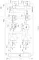
- FIG. 4 is a diagram illustrating a configuration of a device 40a for monitoring a common mode voltage according to an embodiment of the present invention.
- the monitoring device 40a includes an input end 411, voltage dividers 412a and 412b, comparators 413a and 413b, and a controller 414.
- the input end 411 is connected to a node between the battery system 10 which is an energy storage device and the power conversion device 20. A voltage according to the power transferred between the battery system 10 and the power conversion device 20 is applied to the input end 411. A high voltage is applied to the input end 411, and thus, the input end 411 may be configured as a connector having high withstand voltage characteristics.
- the input end 411 is provided with a terminal for measuring a voltage Vp of a cathode line and a terminal for measuring a voltage Vn of an anode line, respectively.
- the voltage dividers 412a and 412b divide the voltage applied to the input end 411. That is, the voltage dividers 412a and 412b serve to lower the applied common mode voltage to a predetermined magnitude.
- the voltage dividers 412a and 412b include a voltage divider 412a for dividing the voltage Vp of the cathode line and a voltage divider 412b for dividing the voltage Vn of the anode line.
- the voltage divider 412a may include a plurality of resistors R1 and R2 for dividing the voltage Vp between the cathode line and the ground into a desired voltage.
- the resistances of the resistors R1 and R2 may be appropriately determined according to the magnitude of the reference voltage used by the comparator 413a.
- the voltage divided by the voltage divider 412a is applied to the comparator 413a.
- a node between the resistors R1 and R2 is connected to the comparator 413a.
- the voltage divider 412b may include a plurality of resistors R4 and R5 for dividing the voltage Vn between the anode line and the ground into a desired voltage.
- the resistances of the resistors R4 and R5 may be appropriately determined according to the magnitude of the reference voltage used by the comparator 413b.
- the voltage divided by the voltage divider 412b is applied to the comparator 413b.
- the node between the resistors R4 and R5 is connected to the comparator 413b.
- Comparators 413a and 413b compare the outputs of the voltage dividers 412a and 412b with a reference voltage Vref1.
- the comparators 413a and 413b compare the voltage obtained by dividing the voltages Vp and Vn of the cathode line and anode line, respectively, by the voltage dividers 412a and 412b with the reference voltage Vref1.
- a non-inverting terminal of the comparator 413a may be connected to the node between the resistors R1 and R2.
- An inverting terminal of the comparator 413a may be connected to a node between the reference voltage Vref1 and a resistor R3.
- the reference voltage Vref1 may be generated by a regulator to be described later.
- a non-inverting terminal of the comparator 413b may be connected to a node between resistors R4 and R5.
- An inverting terminal of the comparator 413b may be connected to a node between the reference voltage Vref1 and a resistor R6.
- a predetermined voltage may be applied to the comparators 413a and 413b as power.
- the voltage applied to the comparators 413a and 413b may be a voltage supplied from a low voltage circuit portion 410 to be described later.
- this is an exemplary configuration, and the power used may be differently set according to the voltage required for the operation of the comparators 413a and 413b.
- a voltage generated by one of a first regulator 415a and a second regulator 415b to be described later may be used as power.
- the controller 414 detects an abnormality in the voltage applied from the power conversion device 20 to the energy storage device based on outputs of the comparators 413a and 413b. That is, the controller 414 determines whether output voltages of the voltage dividers 412a and 412b, which are voltages applied to the non-inverting terminals, exceed the reference voltage based on the outputs of the comparators 413a and 413b. When it is determined that the output voltages of the voltage dividers 412a and 412b exceed the reference voltage, the controller 414 determines that there is an abnormality in the common mode voltage between the power conversion device 20 and the battery system 10. Meanwhile, when it is determined that the output voltages of the voltage dividers 412a and 412b do not exceed the reference voltage, the controller 414 determines that there is no abnormality in the common mode voltage between the power conversion device 20 and the battery system 10.
- the controller 414 transmits an error signal to an external device.
- the controller 414 transmits an error signal to the battery management system of the battery system 10 which is an energy storage device.
- the battery management system of the battery system 10 may be, for example, the rack controller 140 of FIG. 2 , the bank controller 210 of FIG. 3 , etc.
- the controller 414 may transmit the error signal to the battery system controller 30 that is an upper level controller.
- a high voltage circuit portion 400a may be configured to include the input end 411, the voltage dividers 412a and 412b, the comparators 413a and 413b, and the controller 414.
- the high voltage circuit portion 400a is a region that handles a relatively high voltage, and may include a regulator for supplying power therein.
- the first regulator 415a and the second regulator 415b may respectively generate a first reference voltage Vref1 and a second reference voltage Vref2 by using power supplied from the low voltage circuit portion 410.
- the first reference voltage Vref1 generated by the first regulator 415a and the second reference voltage Vref2 generated by the second regulator 415b may be provided to the comparators 413a and 413b or the controller 414.
- the first regulator 415a and the second regulator 415b are included, but is not limited thereto, and one or three or more regulators may be included.
- the high voltage circuit portion 400a may be insulated from and connected to the low voltage circuit portion 410 through isolators.
- the isolators connecting the high voltage circuit portion 400a and the low voltage circuit portion 410 may include a first isolator 420 for power and a second isolator 421 for communication.
- the low voltage circuit unit 410 may include terminal portions 411a and 411b and a power supply portion 412.
- the terminal portions 411a and 411b are components for communicating with the outside.
- Each of the terminal portions 411a and 411b may include a power terminal and a communication terminal.
- the terminal portions 411a and 411b may receive power from the outside using the power terminal.
- the terminal portions 411a and 411b may communicate with an external device through the communication terminal.
- the number of terminal portions may be appropriately determined according to the specification or installation type of the monitoring device 40.
- Power supplied through the terminal portions 411a and 411b is provided to the power supply portion 412.
- the terminal portions 411a and 411b may receive power of 24V from the outside and provide the power to the power supply portion 412.
- the power supply portion 412 may be, for example, a regulator. That is, the power supply portion 412 generates power based on inputs from the terminal portions 411a and 411b.
- the power supply portion 412 may apply the generated voltage to the second isolator 421 as a driving voltage.
- the first isolator 420 supplies power from the low voltage circuit portion 410 to the high voltage circuit portion 400a while insulating the high voltage circuit portion 400a from the low voltage circuit unit 410.
- the first regulator 415a and the second regulator 415b of the high voltage circuit portion 400a generate the first reference voltage Vref1 and the second reference voltage Vref2, respectively, using power transferred through the first isolator 420.
- the second isolator 421 transmits the input from the terminal portions 411a and 411b of the low voltage circuit portion 410 to the controller 414 of the high voltage circuit portion 400a while insulating the high voltage circuit portion 400a from the low voltage circuit portion 410. That is, the second isolator 421 provides a path for the controller 414 to perform communication through the terminal portions 411a and 411b of the low voltage circuit unit 410.
- a line through which a communication signal such as a wake-up signal can be directly transferred may be provided between the terminal portion 411a and the terminal portion 411b.
- the common mode voltage between the power conversion device 20 and the battery system 10 can be accurately monitored by the monitoring device 40a as described above. As a result, it is possible to stably operate the battery system 10 and furthermore the power system 1.
- FIG. 5 is a diagram illustrating a configuration of a common mode voltage monitoring device 40b according to another embodiment of the present invention.
- the monitoring device 40b according to FIG. 5 is different from the monitoring device 40a according to FIG. 4 in the configuration of comparators 413c and 413d of the low-voltage circuit portion 400b, but the other configurations are the same.
- the difference described above will be mainly described.
- the monitoring device 40b monitors the voltage Vp of the cathode line and the voltage Vn of the anode line using a plurality of reference voltages.
- the comparator 413c for monitoring the voltage Vp of the cathode line includes a first comparator 413c1 and a second comparator 413c2.
- the comparator 413d for monitoring the voltage Vn of the anode line includes a third comparator 413d1 and a fourth comparator 413d2.
- the first comparator 413c1 compares the voltage divided by the voltage divider 412a with the reference voltage Vref1, similar to the comparator 413a of FIG. 4 .
- the second comparator 413c2 compares the voltage divided by the voltage divider 412a with the reference voltage Vref2.
- the reference voltage Vref2 is a voltage different from the reference voltage Vref1.
- the third comparator 413d1 also compares the voltage divided by the voltage divider 412b with the reference voltage Vref1, similar to the comparator 413b of FIG. 4 . Further, the fourth comparator 413d2 compares the voltage divided by the voltage divider 412b with the reference voltage Vref2.
- the monitoring device 40b may include the plurality of comparators 413c1, 413c2, 413d1, and 413d2, and at least some of the plurality of comparators may be configured to compare different reference voltages with the output of the voltage divider.
- the controller 414 detects an abnormality in the common mode voltage based on the outputs from the plurality of comparators 413c1, 413c2, 413d1, and 413d2. In this case, the controller 414 may detect whether or not an abnormality occurs in the common mode voltage in the cathode line and a degree of the abnormality based on the outputs of the first comparator 413c1 and second comparator 413c2. For example, it is assumed that the reference voltage Vref1 is greater than the reference voltage Vref2. In this case, if the output from the second comparator 413c2 indicates that the output voltage of the voltage divider 412a does not exceed the reference voltage Vref2, the controller 414 determines that the common mode voltage is normal.
- the controller 414 may determine the abnormality level of the common mode voltage in a plurality of stages based on the plurality of reference voltages described above, and may change a corresponding operation according to the determined abnormality level. For example, when the abnormality level is low, the error may be notified only to the battery system 10, and when the abnormality level is high, the error may be notified to an upper level controller such as the battery system controller 30.
- the monitoring device 40b according to this embodiment may distinguish and grasp the degree of abnormality occurring in the common mode voltage by comparing the common mode voltage with a plurality of reference voltages.
- the monitoring device 40b according to the present embodiment may respond in different ways depending on the abnormality level.
- FIG. 6 is a diagram illustrating a configuration of a common mode voltage monitoring device 40c according to another embodiment of the present invention. Unlike the monitoring device 40a according to FIG. 4 and the monitoring device 40b according to FIG. 5 , the monitoring device 40c according to FIG. 6 includes analog-to-digital converters 416a and 416b instead of the comparators. Hereinafter, the difference described above will be mainly described.
- the monitoring device 40c converts the outputs of the voltage dividers 412a and 412b into digital values in the analog-to-digital converters 416a and 416b, respectively. Then, the digital values, which are the outputs of the analog-to-digital converters 416a and 416b, are applied to the controller 414.
- the controller 414 stores digital values corresponding to a plurality of reference voltages such as reference voltage Vref1 and reference voltage Vref2. Further, the controller 414 compares the digital values applied from the analog-to-digital converters 416a and 416b with a digital value corresponding to the reference voltage. That is, unlike the analog comparison in the monitoring devices 40a and 40b of FIGS. 4 and 5 , in this embodiment, a comparison is made between digital values. Thus, the controller 414 has a function as a comparator.
- the monitoring device 40 is a device connected to the node between the battery system 10 and the power conversion device 20, which is an energy storage device.
- the voltage divider of the monitoring device 40 first divides the voltage between the node between the battery system 10 and the power conversion device 20 and the chassis used as the ground of the battery system 10. Further, the comparator of the monitoring device 40 compares the divided voltage with the reference voltage. Thereafter, the controller of the monitoring device 40 detects an abnormality in the voltage applied from the power conversion device to the energy storage device based on the comparison result.
- the common mode voltage abnormality can be detected by the control method of the monitoring device 40 as described above.
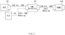
- FIG. 7 is a diagram illustrating an example of a connection configuration of the common mode voltage monitoring device 40 according to the embodiment of the present invention.
- the monitoring device 40 is connected to the rack controller 140 through a terminal portion of the low voltage circuit portion.
- the monitoring device 40 may be connected to the rack controller 140 through a CAN H/L channel to perform communication. Further, for the connection between the monitoring device 40 and the rack controller 140, a line for supplying power and a line for transmitting the wake-up signal are further included.
- the monitoring device 40 is connected to the battery system controller 30 through another terminal portion of the low voltage circuit portion.
- the monitoring device 40 and the battery system controller 30 may only be provided with a CAN H/L channel for communication.
- monitoring devices 40 may be connected to the power supply 50 and supplied with power.
- the monitoring device 40 when the monitoring device 40 detects that an abnormality has occurred in the common mode voltage, the monitoring device 40 may selectively transmit an error notification to the rack controller 140 and the battery system controller 30. The monitoring device 40 may select a destination for transmitting the error notification according to the abnormality level occurring in the common mode voltage.
- FIG. 8 is a diagram illustrating another example of the connection configuration of the common mode voltage monitoring device 40 according to the embodiment of the present invention.
- the monitoring device 40 may be configured to be positioned at a termination and sequentially connected to a bank controller 210a and a bank controller 210b. Further, the battery system controller 30 and the power supply 50 are connected to the bank controller 210b.
- the monitoring device 40 when detecting that an abnormality has occurred in the common mode voltage, transmits the fact that the abnormality has occurred only to the bank controller 210a. Further, the bank controller 210a may determine whether to transmit an error notification to the battery system controller 30 according to the abnormality level generated in the common mode voltage.
- FIG. 9 is a waveform diagram of a voltage measured using the common mode voltage monitoring device according to the embodiment of the present invention.
- the upper waveform shows a case where the common mode voltage is normal.
- the voltage of the cathode line was detected to be approximately 800 V and the voltage of the anode line was detected to be approximately -720 V compared to the ground 0 V (the frequency at which the peak value was represented is approximately 50 kHz). In this case, no error notification has occurred in the monitoring device 40.
- the waveform at the bottom shows a case where the abnormality has occurred in the common mode voltage.
- the common mode voltage was biased toward the negative side due to noise caused by switching of the power converter.
- the voltage of the cathode line was detected to be approximately 500 V
- the voltage of the anode line was detected to be approximately -1050 V (the frequency when the peak value was represented is approximately 50 kHz).
- the value obtained by dividing the common mode voltage in the monitoring device 40 exceeded the reference value, and an abnormality in the common mode voltage was detected.
Landscapes
- Physics & Mathematics (AREA)
- General Physics & Mathematics (AREA)
- Engineering & Computer Science (AREA)
- Power Engineering (AREA)
- Chemical & Material Sciences (AREA)
- Chemical Kinetics & Catalysis (AREA)
- Electrochemistry (AREA)
- General Chemical & Material Sciences (AREA)
- Charge And Discharge Circuits For Batteries Or The Like (AREA)
- Secondary Cells (AREA)
- Protection Of Static Devices (AREA)
- Remote Monitoring And Control Of Power-Distribution Networks (AREA)
Description
- The present invention relates to a device and method for monitoring a common mode voltage.
- Recently, research on a secondary battery as a power supply source is being actively conducted in accordance with the spread of an electronic device such as a smartphone, an uninterruptible power supply (UPS), and an electric vehicle, and expansion of infrastructure for an energy storage device (ESS; energy storage system).
- In the case of an energy storage device, it not only needs to store a large amount of electric energy, but also requires high output. To this end, the energy storage device is used in the form of a battery rack including a plurality of battery modules connected in series and/or in parallel and a charging and discharging device for charging and discharging the plurality of battery modules. The battery module includes battery cells, which are secondary batteries, connected in series and/or in parallel. Further, the battery rack includes a rack controller (RBMS; rack battery management system) for controlling the charging and discharging device, and a plurality of module controllers (MBMS; module battery management system) that respectively control the plurality of battery modules.
- Further, a power conversion device (PCS; power conversion system) is installed outside the energy storage device for charging and discharging. The power conversion device converts AC power of a system into DC power and supplies DC power to the energy storage device, or converts DC power of the energy storage device into AC power and supplies AC power to the system. Switching noise occurs in accordance with switching performed during this power conversion. Switching noise is caused on a common mode voltage transmitted in a power line between the power conversion device and the energy storage device, which affects an operation and safety of a battery system such as the energy storage device. Accordingly, it is necessary to accurately monitor the common mode voltage for stable operation of the battery system.
- Further background art is described in
KR 2018-0066631 A US 2009/184717 A1 ,KR 2019-0012718 A US 2018/088178 A1 andUS 6313750 B1 - The present invention has been made to solve the problems described above, and an object thereof is to accurately detect a common mode voltage transmitted in a power line between the power conversion device and the energy storage device.
- In order to solve the technical problems as described above, according to one aspect of embodiments of the present invention, there is provided a device for monitoring a common mode voltage according to
claim 1. - According to another feature of the device for monitoring the common mode voltage of this embodiment, the comparator may include a plurality of comparators, and at least some of the plurality of comparators may be configured to compare different reference voltages to the output of the voltage divider.
- According to another feature of the device for monitoring the common mode voltage of this embodiment, the comparator may be included in the controller, and may compare a value obtained by converting the output of the voltage divider into a digital value with a digital value corresponding to the reference voltage.
- According to another feature of the device for monitoring the common mode voltage of this embodiment, a terminal portion for communicating with outside of the device, and a power supply portion that generates power based on an input from the terminal portion may be further included.
- According to another feature of the device for monitoring the common mode voltage of this embodiment, an isolator formed between a high voltage circuit portion and a low voltage circuit portion the high voltage circuit portion includes the input end, the voltage divider, the comparator, and the low voltage circuit portion includes the terminal portion and the power supply portion to insulate the high voltage circuit portion from the low voltage circuit portion.
- According to another feature of the device for monitoring the common mode voltage of this embodiment, the isolator may include a power isolator for supplying power from the low voltage circuit portion to the high voltage circuit portion, and a communication isolator for transmitting an input from the terminal portion to the controller.
- According to another feature of the device for monitoring the common mode voltage of this embodiment, the controller may transmit an error signal to outside of the device when an abnormality is detected, by the controller, in the voltage applied to the energy storage device.
- According to another feature of the device for monitoring the common mode voltage of this embodiment, the controller may transmit the error signal to a battery management system of the energy storage device.
- According to another feature of the device for monitoring the common mode voltage of this embodiment, the controller may transmit the error signal to an upper level controller that manages the energy storage device.
- According to another feature of the device for monitoring the common mode voltage of this embodiment, the voltage applied to the input end may be a voltage between the node and a chassis that is the ground of the energy storage device.
- In order to solve the technical problems as described above, according to another aspect of embodiments of the present invention, there is provided a method of controlling a device for monitoring a common mode voltage connected to a node between an energy storage device and a power conversion device according to claim 11.
- According to the device and method for monitoring the common mode voltage described above, it is possible to accurately detect the common mode voltage transferred in the power line between the conversion device and the energy storage device, thereby enabling stable operation of the battery system.
-
-
FIG. 1 is a diagram schematically illustrating a configuration of an energy storage system to which a device for monitoring a common mode voltage according to an embodiment of the present invention is applied; -
FIG. 2 is a diagram illustrating a configuration of a battery system according to an embodiment of the present invention; -
FIG. 3 is a diagram illustrating the configuration of the battery system according to another embodiment of the present invention; -
FIG. 4 is a diagram illustrating a configuration of the device for monitoring the common mode voltage according to an embodiment of the present invention; -
FIG. 5 is a diagram illustrating the configuration of the device for monitoring the common mode voltage according to another embodiment of the present invention; -
FIG. 6 is a diagram illustrating the configuration of the device for monitoring the common mode voltage according to still another embodiment of the present invention; -
FIG. 7 is a diagram illustrating a connection configuration of the device for monitoring the common mode voltage according to the embodiment of the present invention; -
FIG. 8 is a diagram illustrating another example of the connection configuration of the device for monitoring the common mode voltage according to the embodiment of the present invention; and -
FIG. 9 is a waveform diagram of a voltage measured using the device for monitoring the common mode voltage according to the embodiment of the present invention. - Hereinafter, various embodiments of the present invention will be described in detail with reference to the accompanying drawings. In this document, the same reference numerals are used for the same constituent elements in the drawings, and duplicate descriptions for the same constituent elements are omitted.
- With respect to the various embodiments of the present invention disclosed in this document, specific structural or functional descriptions have been exemplified for the purpose of describing the embodiments of the present invention only, and various embodiments of the present invention may be embodied in various forms and should not be construed as being limited to the embodiments described in this document.
- Expressions such as "first", "second", "firstly", or "secondly", etc. used in various embodiments may modify various constituent elements regardless of order and/or importance, and do not limit corresponding constituent elements. For example, without deviating from the scope of the present invention, a first constituent element may be named as a second constituent element, and similarly, the second constituent element may also be renamed as the first constituent element.
- The terms used in this document are only used to describe a specific embodiment, and may not be intended to limit the scope of other embodiments. Singular expressions may include plural expressions unless the context clearly indicates otherwise.
-
FIG. 1 is a diagram schematically illustrating a configuration of an energy storage system to which a device for monitoring a common mode voltage according to an embodiment of the present invention is applied. - Referring to
FIG. 1 , apower system 1 is a system that is connected to asystem 2 to receive power or supply power to thesystem 2 and a load. Thepower system 1 includes abattery system 10, apower conversion device 20, abattery system controller 30, and adevice 40 for monitoring a common mode voltage (hereinafter, simply referred to as a 'monitoring device'). - The
battery system 10 refers to an energy storage device that stores power. Thebattery system 10 may be provided in the form of a battery rack or a battery bank including a plurality of battery racks. Thebattery system 10 may be charged using DC power supplied from thepower conversion device 20. Thebattery system 10 may perform a discharging operation by outputting DC power and supplying DC power to thepower conversion device 20. - The operation of the
battery system 10 may be controlled by a battery system controller (BSC) 30. Thebattery system 10 communicates with thebattery system controller 30 to transmit data related to thebattery system 10. For example, thebattery system 10 may transmit a value obtained by measuring the temperature and voltage of thebattery system 10 or parameters such as SOC and SOH derived therefrom to thebattery system controller 30. Although not illustrated, in thebattery system 10, various devices for monitoring a state of thebattery system 10 and a controller for communication with thebattery system controller 30 may be provided therein. - The
power conversion device 20 converts AC power supplied from thesystem 2 into DC power. Thepower conversion device 20 supplies the converted DC power to thebattery system 10. Thepower conversion device 20 converts DC power supplied from thebattery system 10 into AC power. Thepower conversion device 20 supplies the converted AC power to thesystem 2. Further, although not illustrated, thepower conversion device 20 may supply the converted AC power to the load. - The
power conversion device 20 may include an inverter and a converter for conversion between DC power and AC power. Thepower conversion device 20 may perform a power conversion operation under the control of thebattery system controller 30. - The
battery system controller 30 manages each component included in thepower system 1 and controls the overall operation. Thebattery system controller 30 may communicate with a controller provided in thebattery system 1. Thebattery system controller 30 may transmit a control signal to thebattery system 1 to control the operation of thebattery system 1. Further, thebattery system controller 30 may receive data from thebattery system 1 and manage the state of thebattery system 1. Thebattery system controller 30 may transmit a control signal to thepower conversion device 20 to control a power conversion operation of thepower conversion device 30. - The
battery system controller 30 also receives a monitoring result of a common mode voltage between thepower conversion device 20 and thebattery system 10 which is an energy storage device from themonitoring device 40. When thebattery system controller 30 receives a notification that there is an abnormality in the common mode voltage from themonitoring device 40, thebattery system controller 30 may transmit the notification to the outside. For example, thebattery system controller 30 may be a subject operating thepower system 1. - The
monitoring device 40 monitors the common mode voltage between thepower conversion device 20 and thebattery system 10 which is an energy storage device. That is, themonitoring device 40 monitors the voltage between a cathode line between thepower conversion device 20 and thebattery system 10 and a reference potential (e.g., ground). Further, themonitoring device 40 monitors the voltage between an anode line between thepower conversion device 20 and thebattery system 10 and a reference potential (e.g., ground). The reference potential in this case may be the ground of thebattery system 10, for example, a chassis of the battery rack. - When an abnormality is found in the measured voltage, the
monitoring device 40 transmits the fact that the abnormality is found in the measured voltage to thebattery system controller 30. Themonitoring device 40 transmits an alarm or warning indicating an abnormality in the common mode voltage to thebattery system controller 30. - Hereinafter, a configuration of the
battery system 10 will be described in more detail. -
FIG. 2 is a diagram illustrating a configuration of abattery system 10a according to an embodiment of the present invention. - The
battery system 10a according to the present embodiment may be abattery rack 100. Thebattery rack 100 includes a plurality of battery modules 110-1 to 110-n each including a battery pack (battery cell assembly) 120 and a module controller (MBMS) 130. Thebattery rack 100 further includes a charging and dischargingdevice 150 for charging and discharging thebattery module 110 and a rack controller (RBMS) 140. (In this embodiment, when there is no need to distinguish between the battery modules, the module controllers, and the battery packs, reference numerals thereof will be denoted as 110, 120, and 130, respectively.) - The
battery module 110 is a component that is mounted on thebattery rack 100 to store power. A plurality ofbattery modules 110 may be provided according to specifications required for thebattery rack 100. The plurality ofbattery modules 110 may be connected in series and/or parallel within thebattery rack 110 to provide a required output. Thebattery module 110 includes abattery pack 120 that stores power and amodule controller 130 that controls the operation of thebattery pack 120. - The
battery pack 120 is a component that stores power and includes a plurality of battery cells. Thebattery pack 120 may include a plurality of battery cells connected in series and/or in parallel. The number and connection type of the battery cells may be determined according to the required output of thebattery pack 120. The battery cell included in thebattery pack 120 may be a secondary battery such as a lithium ion (Li-ion) battery, a lithium ion polymer battery, a nickel cadmium (Ni-Cd) battery, and a nickel hydride (Ni-MH) battery, but is not limited thereto. - The
module controller 130 controls charging and discharging of thebattery pack 120, and manages the state thereof. Themodule controller 130 may monitor voltage, current, temperature, etc. of thebattery pack 120. Further, themodule controller 130 may additionally include a sensor or various measurement modules (not illustrated) for monitoring. Themodule controller 40 may calculate parameters indicating the state of thebattery pack 120, for example, SOC or SOH, based on measured values such as the monitored voltage, current, and temperature. - The
module controller 130 may be configured to communicate with therack controller 140. Themodule controller 40 may receive a control signal such as a command for controlling thebattery pack 120 from therack controller 140. Themodule controller 130 may transmit the measured value by the monitoring described above or the parameter calculated from the measured value to therack controller 140. - The
rack controller 140 and a plurality of module controllers 130-1 to 130-n are collectively referred to as a battery management system (BMS). Therack controller 20 of the battery management system (BMS) and the plurality of module controllers 40-1 to 40-n may perform communication in a wired and/or wireless manner. For example, when wired communication is applied within the battery management system, communication may be performed with each other using a communication protocol of differential input mode. Examples of the communication protocol of differential input mode include controller area network (CAN) recommended standard 485 (RS-485), recommended standard 422 (RS-422), etc. Further, when wireless communication is applied within the battery management system, wireless communication protocols such as wi-fi (registered trademark) and Bluetooth (registered trademark) may be used. However, the wired and wireless communication protocols are only examples, and are not limited thereto. - The charging and discharging
device 150 charges and discharges thebattery module 110. The charging and dischargingdevice 150 supplies power to thebattery module 110 or supplies power from thebattery module 110 to a system or a load. The charging and dischargingdevice 150 may be connected to a system to receive power from the system, and may supply the received power to thebattery module 110. Further, the charging and dischargingdevice 150 may supply power discharged from thebattery module 110 to the system or the load (e.g., a factory, a home, etc.). The charging and dischargingdevice 150 may include a switching device for charging and discharging thebattery module 110, for example, a relay. - The
battery system 10a may be provided in the form of abattery rack 100 as described above and connected to thepower conversion device 20. -
FIG. 3 is a diagram illustrating a configuration of abattery system 10b according to another embodiment of the present invention. - The
battery system 10b according to this embodiment may be abattery bank 200. Thebattery bank 200 includes a plurality of battery racks 100-1 to 100-m and a bank controller (BBMS; bank battery management system) 210. - Each of the plurality of battery racks 100-1 to 100-n corresponds to the
battery rack 100 described inFIG. 2 . Each of thesebattery racks 100 include a rack controller (RBMS) that manages thebattery rack 100 and controls its operation. - The
bank controller 210 may receive various data by performing communication with the rack controllers (RBMS) included in the plurality of battery racks 100. Further, thebank controller 210 may control the operation of thebattery rack 100 by transmitting a control signal to the rack controller (RBMS). To this end, thebank controller 210 may perform communication with the rack controller (RBMS) in a wired or wireless manner. A protocol for wired or wireless communication is not particularly limited, and a protocol suitable for operating thebattery bank 200 may be selected. Further, in this embodiment, a plurality ofbattery racks 100 are illustrated to be included in thebattery bank 200, but is not limited thereto, and only asingle battery rack 100 may be included therein. - The
battery system 10a may be provided in the form of thebattery bank 200 as described above and may be connected to thepower conversion device 20. - Hereinafter, the
monitoring device 40 that may be installed between thebattery system 10 and thepower conversion device 20 described above will be described in detail. -
FIG. 4 is a diagram illustrating a configuration of adevice 40a for monitoring a common mode voltage according to an embodiment of the present invention. - The
monitoring device 40a includes aninput end 411,voltage dividers comparators controller 414. - The
input end 411 is connected to a node between thebattery system 10 which is an energy storage device and thepower conversion device 20. A voltage according to the power transferred between thebattery system 10 and thepower conversion device 20 is applied to theinput end 411. A high voltage is applied to theinput end 411, and thus, theinput end 411 may be configured as a connector having high withstand voltage characteristics. Theinput end 411 is provided with a terminal for measuring a voltage Vp of a cathode line and a terminal for measuring a voltage Vn of an anode line, respectively. - The
voltage dividers input end 411. That is, thevoltage dividers voltage dividers voltage divider 412a for dividing the voltage Vp of the cathode line and avoltage divider 412b for dividing the voltage Vn of the anode line. - The
voltage divider 412a may include a plurality of resistors R1 and R2 for dividing the voltage Vp between the cathode line and the ground into a desired voltage. The resistances of the resistors R1 and R2 may be appropriately determined according to the magnitude of the reference voltage used by thecomparator 413a. The voltage divided by thevoltage divider 412a is applied to thecomparator 413a. In thevoltage divider 412a, a node between the resistors R1 and R2 is connected to thecomparator 413a. - Similarly, the
voltage divider 412b may include a plurality of resistors R4 and R5 for dividing the voltage Vn between the anode line and the ground into a desired voltage. The resistances of the resistors R4 and R5 may be appropriately determined according to the magnitude of the reference voltage used by thecomparator 413b. The voltage divided by thevoltage divider 412b is applied to thecomparator 413b. In thevoltage divider 412b, the node between the resistors R4 and R5 is connected to thecomparator 413b. -
Comparators voltage dividers comparators voltage dividers comparator 413a may be connected to the node between the resistors R1 and R2. An inverting terminal of thecomparator 413a may be connected to a node between the reference voltage Vref1 and a resistor R3. The reference voltage Vref1 may be generated by a regulator to be described later. Similarly, a non-inverting terminal of thecomparator 413b may be connected to a node between resistors R4 and R5. An inverting terminal of thecomparator 413b may be connected to a node between the reference voltage Vref1 and a resistor R6. - A predetermined voltage may be applied to the
comparators comparators voltage circuit portion 410 to be described later. However, this is an exemplary configuration, and the power used may be differently set according to the voltage required for the operation of thecomparators first regulator 415a and asecond regulator 415b to be described later may be used as power. - The controller 414 (MCU) detects an abnormality in the voltage applied from the
power conversion device 20 to the energy storage device based on outputs of thecomparators controller 414 determines whether output voltages of thevoltage dividers comparators voltage dividers controller 414 determines that there is an abnormality in the common mode voltage between thepower conversion device 20 and thebattery system 10. Meanwhile, when it is determined that the output voltages of thevoltage dividers controller 414 determines that there is no abnormality in the common mode voltage between thepower conversion device 20 and thebattery system 10. - When it is determined that there is an abnormality in the common mode voltage, the
controller 414 transmits an error signal to an external device. For example, thecontroller 414 transmits an error signal to the battery management system of thebattery system 10 which is an energy storage device. The battery management system of thebattery system 10 may be, for example, therack controller 140 ofFIG. 2 , thebank controller 210 ofFIG. 3 , etc. Alternatively, thecontroller 414 may transmit the error signal to thebattery system controller 30 that is an upper level controller. - A high
voltage circuit portion 400a may be configured to include theinput end 411, thevoltage dividers comparators controller 414. The highvoltage circuit portion 400a is a region that handles a relatively high voltage, and may include a regulator for supplying power therein. Thefirst regulator 415a and thesecond regulator 415b may respectively generate a first reference voltage Vref1 and a second reference voltage Vref2 by using power supplied from the lowvoltage circuit portion 410. The first reference voltage Vref1 generated by thefirst regulator 415a and the second reference voltage Vref2 generated by thesecond regulator 415b may be provided to thecomparators controller 414. In this embodiment, thefirst regulator 415a and thesecond regulator 415b are included, but is not limited thereto, and one or three or more regulators may be included. - Meanwhile, the high
voltage circuit portion 400a may be insulated from and connected to the lowvoltage circuit portion 410 through isolators. The isolators connecting the highvoltage circuit portion 400a and the lowvoltage circuit portion 410 may include afirst isolator 420 for power and asecond isolator 421 for communication. - The low
voltage circuit unit 410 may includeterminal portions power supply portion 412. - The
terminal portions terminal portions terminal portions terminal portions monitoring device 40. - Power supplied through the
terminal portions power supply portion 412. For example, theterminal portions power supply portion 412. Thepower supply portion 412 may be, for example, a regulator. That is, thepower supply portion 412 generates power based on inputs from theterminal portions power supply portion 412 may apply the generated voltage to thesecond isolator 421 as a driving voltage. - The
first isolator 420 supplies power from the lowvoltage circuit portion 410 to the highvoltage circuit portion 400a while insulating the highvoltage circuit portion 400a from the lowvoltage circuit unit 410. Thefirst regulator 415a and thesecond regulator 415b of the highvoltage circuit portion 400a generate the first reference voltage Vref1 and the second reference voltage Vref2, respectively, using power transferred through thefirst isolator 420. - The
second isolator 421 transmits the input from theterminal portions voltage circuit portion 410 to thecontroller 414 of the highvoltage circuit portion 400a while insulating the highvoltage circuit portion 400a from the lowvoltage circuit portion 410. That is, thesecond isolator 421 provides a path for thecontroller 414 to perform communication through theterminal portions voltage circuit unit 410. - Meanwhile, as illustrated in
FIG. 4 , a line through which a communication signal such as a wake-up signal can be directly transferred may be provided between theterminal portion 411a and theterminal portion 411b. - The common mode voltage between the
power conversion device 20 and thebattery system 10 can be accurately monitored by themonitoring device 40a as described above. As a result, it is possible to stably operate thebattery system 10 and furthermore thepower system 1. - Further, when an abnormality in the common mode voltage is detected, it means that noise caused by the switching of the
power conversion device 20 is large, and thus it is possible to prevent a larger failure in advance by checking thepower conversion device 20. -
FIG. 5 is a diagram illustrating a configuration of a common modevoltage monitoring device 40b according to another embodiment of the present invention. Themonitoring device 40b according toFIG. 5 is different from themonitoring device 40a according toFIG. 4 in the configuration ofcomparators voltage circuit portion 400b, but the other configurations are the same. Hereinafter, the difference described above will be mainly described. - Referring to
FIG. 5 , themonitoring device 40b according to this embodiment monitors the voltage Vp of the cathode line and the voltage Vn of the anode line using a plurality of reference voltages. To this end, thecomparator 413c for monitoring the voltage Vp of the cathode line includes a first comparator 413c1 and a second comparator 413c2. Further, thecomparator 413d for monitoring the voltage Vn of the anode line includes a third comparator 413d1 and a fourth comparator 413d2. - The first comparator 413c1 compares the voltage divided by the
voltage divider 412a with the reference voltage Vref1, similar to thecomparator 413a ofFIG. 4 . The second comparator 413c2 compares the voltage divided by thevoltage divider 412a with the reference voltage Vref2. The reference voltage Vref2 is a voltage different from the reference voltage Vref1. - The third comparator 413d1 also compares the voltage divided by the
voltage divider 412b with the reference voltage Vref1, similar to thecomparator 413b ofFIG. 4 . Further, the fourth comparator 413d2 compares the voltage divided by thevoltage divider 412b with the reference voltage Vref2. - As described above, the
monitoring device 40b may include the plurality of comparators 413c1, 413c2, 413d1, and 413d2, and at least some of the plurality of comparators may be configured to compare different reference voltages with the output of the voltage divider. - The
controller 414 detects an abnormality in the common mode voltage based on the outputs from the plurality of comparators 413c1, 413c2, 413d1, and 413d2. In this case, thecontroller 414 may detect whether or not an abnormality occurs in the common mode voltage in the cathode line and a degree of the abnormality based on the outputs of the first comparator 413c1 and second comparator 413c2. For example, it is assumed that the reference voltage Vref1 is greater than the reference voltage Vref2. In this case, if the output from the second comparator 413c2 indicates that the output voltage of thevoltage divider 412a does not exceed the reference voltage Vref2, thecontroller 414 determines that the common mode voltage is normal. While the output from the second comparator 413c2 indicates that the output voltage of thevoltage divider 412a exceeds the reference voltage Vref2, if the output from the first comparator 413c1 indicates that the output voltage of thevoltage divider 412a does not exceed the reference voltage Vref1, thecontroller 414 determines that an abnormality level of the common mode voltage is 1. Finally, if the output from the first comparator 413c1 indicates that the output voltage of thevoltage divider 412a exceeds the reference voltage Vref1, thecontroller 414 determines that the abnormality level of the common mode voltage is 2. This operation may be similarly applied to the third comparator 413d1 and the fourth comparator 413d2. - The
controller 414 may determine the abnormality level of the common mode voltage in a plurality of stages based on the plurality of reference voltages described above, and may change a corresponding operation according to the determined abnormality level. For example, when the abnormality level is low, the error may be notified only to thebattery system 10, and when the abnormality level is high, the error may be notified to an upper level controller such as thebattery system controller 30. - Even when the
monitoring device 40b described above is used, it is possible to accurately monitor the common mode voltage, similar to themonitoring device 40a according toFIG. 4 . As a result, it is possible to stably operate thebattery system 10 and furthermore thepower system 1. - Further, the
monitoring device 40b according to this embodiment may distinguish and grasp the degree of abnormality occurring in the common mode voltage by comparing the common mode voltage with a plurality of reference voltages. Themonitoring device 40b according to the present embodiment may respond in different ways depending on the abnormality level. -
FIG. 6 is a diagram illustrating a configuration of a common modevoltage monitoring device 40c according to another embodiment of the present invention. Unlike themonitoring device 40a according toFIG. 4 and themonitoring device 40b according toFIG. 5 , themonitoring device 40c according toFIG. 6 includes analog-to-digital converters - Referring to
FIG. 6 , themonitoring device 40c according to this embodiment converts the outputs of thevoltage dividers digital converters digital converters controller 414. - The
controller 414 stores digital values corresponding to a plurality of reference voltages such as reference voltage Vref1 and reference voltage Vref2. Further, thecontroller 414 compares the digital values applied from the analog-to-digital converters monitoring devices FIGS. 4 and5 , in this embodiment, a comparison is made between digital values. Thus, thecontroller 414 has a function as a comparator. - Even when the
monitoring device 40c as described above is used, it is possible to accurately monitor the common mode voltage. As a result, it is possible to stably operate thebattery system 10 and furthermore thepower system 1. - In summary, the
monitoring device 40 is a device connected to the node between thebattery system 10 and thepower conversion device 20, which is an energy storage device. The voltage divider of themonitoring device 40 first divides the voltage between the node between thebattery system 10 and thepower conversion device 20 and the chassis used as the ground of thebattery system 10. Further, the comparator of themonitoring device 40 compares the divided voltage with the reference voltage. Thereafter, the controller of themonitoring device 40 detects an abnormality in the voltage applied from the power conversion device to the energy storage device based on the comparison result. The common mode voltage abnormality can be detected by the control method of themonitoring device 40 as described above. -
FIG. 7 is a diagram illustrating an example of a connection configuration of the common modevoltage monitoring device 40 according to the embodiment of the present invention. - Referring to
FIG. 7 , themonitoring device 40 is connected to therack controller 140 through a terminal portion of the low voltage circuit portion. Themonitoring device 40 may be connected to therack controller 140 through a CAN H/L channel to perform communication. Further, for the connection between themonitoring device 40 and therack controller 140, a line for supplying power and a line for transmitting the wake-up signal are further included. - Further, the
monitoring device 40 is connected to thebattery system controller 30 through another terminal portion of the low voltage circuit portion. Themonitoring device 40 and thebattery system controller 30 may only be provided with a CAN H/L channel for communication. - In addition, the
monitoring devices 40 may be connected to thepower supply 50 and supplied with power. - In the case of the connection configuration according to
FIG. 7 , when themonitoring device 40 detects that an abnormality has occurred in the common mode voltage, themonitoring device 40 may selectively transmit an error notification to therack controller 140 and thebattery system controller 30. Themonitoring device 40 may select a destination for transmitting the error notification according to the abnormality level occurring in the common mode voltage. -
FIG. 8 is a diagram illustrating another example of the connection configuration of the common modevoltage monitoring device 40 according to the embodiment of the present invention. - Referring to
FIG. 8 , themonitoring device 40 may be configured to be positioned at a termination and sequentially connected to abank controller 210a and abank controller 210b. Further, thebattery system controller 30 and thepower supply 50 are connected to thebank controller 210b. - In the case of the connection configuration according to
FIG. 8 , when detecting that an abnormality has occurred in the common mode voltage, themonitoring device 40 transmits the fact that the abnormality has occurred only to thebank controller 210a. Further, thebank controller 210a may determine whether to transmit an error notification to thebattery system controller 30 according to the abnormality level generated in the common mode voltage. -
FIG. 9 is a waveform diagram of a voltage measured using the common mode voltage monitoring device according to the embodiment of the present invention. - Referring to
FIG. 9 , the upper waveform shows a case where the common mode voltage is normal. When the common mode voltage is normal, the voltage of the cathode line was detected to be approximately 800 V and the voltage of the anode line was detected to be approximately -720 V compared to the ground 0 V (the frequency at which the peak value was represented is approximately 50 kHz). In this case, no error notification has occurred in themonitoring device 40. - Meanwhile, the waveform at the bottom shows a case where the abnormality has occurred in the common mode voltage. As can be seen from the waveform, the common mode voltage was biased toward the negative side due to noise caused by switching of the power converter. The voltage of the cathode line was detected to be approximately 500 V, and the voltage of the anode line was detected to be approximately -1050 V (the frequency when the peak value was represented is approximately 50 kHz). In this case, the value obtained by dividing the common mode voltage in the
monitoring device 40 exceeded the reference value, and an abnormality in the common mode voltage was detected. - As described above, it was confirmed that the abnormality of the common mode voltage through the
monitoring device 40 can be accurately monitored. - Further, the terms such as "include", "configure" or "have" described above mean that the corresponding constituent element may be embedded unless otherwise described, and thus the terms should be interpreted as being capable of further including other constituent elements, rather than excluding other constituent elements. All terms used herein including technical or scientific terms may be interpreted as having the same meaning as generally understood by a person of ordinary skill in the art, unless otherwise defined. Terms generally used, such as terms defined in the dictionary, should be interpreted as being consistent with the meaning of the context of related technology, and are not to be interpreted as an ideal or excessively formal meaning unless explicitly defined in the present invention.
- The above description is merely illustrative of the technical idea of the present invention, and those of ordinary skill in the art to which the present invention pertains will be able to make various modifications and variations without deviating from the essential characteristics of the present invention. Accordingly, the embodiments disclosed in the present invention are not intended to limit the technical idea of the present invention, but to explain the technical idea, and the scope of the technical idea of the present invention is not limited by these embodiments. The scope of protection of the present invention should be interpreted by the claims set forth below.
Claims (11)
- A device (40, 40a) for monitoring a common mode voltage between a power conversion device (20) and an energy storage device (10), the device comprising:an input end (411) connected to a node between the energy storage device and the power conversion device;a voltage divider (412a, 412b) configured to divide a voltage applied to the input end;a comparator (413a, 413b; 413c1, 413c2, 413d1, 413d2) configured to compare an output of the voltage divider and a reference voltage (Vref1); anda controller (414) configured to detect an abnormality in a voltage applied from the power conversion device to the energy storage device based on an output of the comparator;characterized in that the input end is provided with a terminal for measuring a voltage (Vp) of a cathode line and a terminal for measuring a voltage (Vn) of an anode line between the energy storage device and the power conversion device;wherein the voltage divider comprises a first voltage divider (412a) configured to divide the voltage of the cathode line and a second voltage divider configured to divide the voltage of the anode line;wherein the comparator comprises a first comparator (413a; 413c1) configured to compare the voltage obtained by dividing the voltage of the cathode line by the first voltage divider with the reference voltage, and a second comparator (413b; 413d1) configured to compare the voltage obtained by dividing the voltage of the anode line by the second voltage divider with the reference voltage;wherein the controller is configured to detect an abnormality based on the outputs of both comparators.
- The device of claim 1,
wherein the comparator further includes a third comparator (413c2) configured to compare the voltage divided by the first voltage divider with another reference voltage (Vref2) different from the reference voltage (Vref1), and a fourth comparator (413d2) configured to compare the voltage divided by the second voltage divider with the other reference voltage (Vref2). - The device of claim 1,
wherein the comparator is included in the controller, and is configured to compare a value obtained by converting the output of the voltage divider into a digital value with a digital value corresponding to the reference voltage. - The device of claim 1, further comprising:a terminal portion (411a, 411b) configured to communicate with outside of the device, anda power supply portion (412) configured to generate power based on an input from the terminal portion.
- The device of claim 4, further comprising:an isolator (420, 421) formed between a high voltage circuit portion (400a) and a low voltage circuit portion (410),wherein the high voltage circuit portion includes the input end, the voltage divider, the comparator, andwherein the low voltage circuit portion includes the terminal portion and the power supply portion to insulate the high voltage circuit portion from the low voltage circuit portion.
- The device of claim 5,
wherein the isolator includes:a power isolator (420) configured to supply power from the low voltage circuit portion to the high voltage circuit portion; anda communication isolator (421) configured to transmit an input from the terminal portion to the controller. - The device of claim 1,
wherein the controller is configured to transmit an error signal to outside of the device when an abnormality is detected, by the controller, in the voltage applied to the energy storage device. - The device of claim 7,
wherein the controller is configured to transmit the error signal to a battery management system of the energy storage device. - The device of claim 7,
wherein the controller is configured to transmit the error signal to an upper level controller that manages the energy storage device. - The device of claim 1,
wherein the voltage applied to the input end is a voltage between the node and a chassis that is the ground of the energy storage device. - A method of controlling a device for monitoring a common mode voltage between an energy storage device and a power conversion device on a cathode line and on an anode line, the method comprising:measuring a voltage of the cathode line and a voltage of the anode line;dividing the voltage of the cathode line and the voltage of the anode line;comparing the divided voltage of the cathode line and the anode line with a reference voltage; anddetecting an abnormality in a voltage applied from the power conversion device to the energy storage device based on the results of the comparison.
Applications Claiming Priority (2)
| Application Number | Priority Date | Filing Date | Title |
|---|---|---|---|
| KR1020200011239A KR102843295B1 (en) | 2020-01-30 | 2020-01-30 | Device and method for monitoring common mode voltage |
| PCT/KR2021/000307 WO2021153923A1 (en) | 2020-01-30 | 2021-01-11 | Common mode voltage monitoring device and monitoring method |
Publications (3)
| Publication Number | Publication Date |
|---|---|
| EP3995840A1 EP3995840A1 (en) | 2022-05-11 |
| EP3995840A4 EP3995840A4 (en) | 2022-12-14 |
| EP3995840B1 true EP3995840B1 (en) | 2024-06-12 |
Family
ID=77078386
Family Applications (1)
| Application Number | Title | Priority Date | Filing Date |
|---|---|---|---|
| EP21748242.1A Active EP3995840B1 (en) | 2020-01-30 | 2021-01-11 | Device and method for monitoring common mode voltage |
Country Status (10)
| Country | Link |
|---|---|
| US (1) | US12032005B2 (en) |
| EP (1) | EP3995840B1 (en) |
| JP (1) | JP7285968B2 (en) |
| KR (1) | KR102843295B1 (en) |
| CN (1) | CN114127566B (en) |
| AU (1) | AU2021213624B2 (en) |
| ES (1) | ES2984816T3 (en) |
| HU (1) | HUE067030T2 (en) |
| PL (1) | PL3995840T3 (en) |
| WO (1) | WO2021153923A1 (en) |
Families Citing this family (3)
| Publication number | Priority date | Publication date | Assignee | Title |
|---|---|---|---|---|
| US11881708B2 (en) * | 2022-06-09 | 2024-01-23 | Hamilton Sundstrand Corporation | Common mode voltage feed fault protection |
| US12352825B2 (en) * | 2022-06-09 | 2025-07-08 | Hamilton Sundstrand Corporation | Common mode voltage feed fault protection |
| US12519412B2 (en) | 2022-06-09 | 2026-01-06 | Hamilton Sundstrand Corporation | Common mode current feed fault protection |
Family Cites Families (34)
| Publication number | Priority date | Publication date | Assignee | Title |
|---|---|---|---|---|
| JP2838462B2 (en) | 1992-11-09 | 1998-12-16 | 松下電器産業株式会社 | Earth leakage detection device |
| JP3041150B2 (en) | 1993-02-15 | 2000-05-15 | 松下電器産業株式会社 | Earth leakage detection device |
| JP3480019B2 (en) | 1993-12-29 | 2003-12-15 | 松下電工株式会社 | Leakage determination method and device |
| JPH10213611A (en) * | 1997-01-28 | 1998-08-11 | Matsushita Electric Ind Co Ltd | Power supply voltage drop detection device and its detection method |
| KR20000075877A (en) | 1997-03-07 | 2000-12-26 | 도날드 디. 먼둘 | Voltage divider providing switchable resolution |
| JP4106496B2 (en) | 1997-12-26 | 2008-06-25 | 株式会社安川電機 | Inverter common mode voltage / current suppression method and apparatus |
| KR20000010233A (en) | 1998-07-31 | 2000-02-15 | 김태구 | Overvoltage prevention device of alternator |
| US6313750B1 (en) | 1999-08-23 | 2001-11-06 | Plug Power Inc. | Measuring cell voltages of a fuel cell stack |
| US9270133B2 (en) | 2007-04-02 | 2016-02-23 | Linear Technology Corporation | Monitoring cells in energy storage system |
| US8022710B2 (en) | 2008-01-18 | 2011-09-20 | GM Global Technology Operations LLC | Methods for common mode voltage-based AC fault detection, verification and/or identification |
| JP2010261862A (en) | 2009-05-08 | 2010-11-18 | Sony Corp | AC line signal detection device and method, and power supply device |
| KR20120073520A (en) * | 2010-12-27 | 2012-07-05 | 주식회사 이아이지 | Battery management system and battery monitoring system using the same |
| JP5353915B2 (en) * | 2011-02-01 | 2013-11-27 | 株式会社デンソー | Battery voltage monitoring device |
| US9341665B2 (en) * | 2012-04-18 | 2016-05-17 | Lear Corporation | Method and apparatus for high voltage isolation monitor for a vehicle |
| KR101631064B1 (en) * | 2012-08-06 | 2016-06-16 | 삼성에스디아이 주식회사 | Battery pack, voltage measuring method of the same, and energy storage system including the battery pack |
| US9178421B2 (en) * | 2012-10-30 | 2015-11-03 | Nvidia Corporation | Multi-stage power supply with fast transient response |
| JP2014103819A (en) | 2012-11-22 | 2014-06-05 | Nemoto Denko Co Ltd | Charging device, charging method, power supply system and residual stored power amount measuring method thereof |
| JP2014147161A (en) * | 2013-01-28 | 2014-08-14 | Toyota Motor Corp | Vehicle |
| KR101522475B1 (en) | 2013-12-30 | 2015-05-21 | 주식회사 효성 | Method and apparatus for charging battery |
| CN104007391A (en) | 2014-04-29 | 2014-08-27 | 江苏华东锂电技术研究院有限公司 | Temperature and voltage monitoring system of lithium battery pack |
| KR101592702B1 (en) * | 2014-06-10 | 2016-02-15 | 현대자동차주식회사 | Apparatus and method for reducing common mode voltage |
| KR101711706B1 (en) | 2014-11-20 | 2017-03-02 | 주식회사 엘지화학 | Common Mode Noise Simulator |
| US9599651B2 (en) | 2015-02-19 | 2017-03-21 | Nec Energy Solutions, Inc. | Systems and methods of detecting ground faults in energy storage and/or generation systems that employ DC/AC power conversion systems |
| JP6497298B2 (en) * | 2015-11-10 | 2019-04-10 | 株式会社デンソー | Abnormality diagnosis device |
| JP6611619B2 (en) * | 2016-01-12 | 2019-11-27 | アルパイン株式会社 | Power fluctuation detection device and processing system |
| JP6699485B2 (en) | 2016-09-23 | 2020-05-27 | 株式会社デンソー | Voltage detector |
| CN106451772A (en) * | 2016-10-08 | 2017-02-22 | 广州供电局有限公司 | Direct voltage acquisition apparatus |
| KR101887905B1 (en) * | 2016-12-09 | 2018-08-13 | 현대오트론 주식회사 | An Apparatus And A Method For Monitoring High Voltage Battery And Detecting Over/Under Voltage |
| KR101769357B1 (en) * | 2017-03-02 | 2017-08-30 | (주) 파루 | Energy storage system capable of controling power quality, monitoring system using it and the monitoring method thereof |
| KR102410938B1 (en) * | 2017-06-20 | 2022-06-20 | 현대자동차주식회사 | Apparatus for managing power of vehicle and method for controlling the same |
| KR102323035B1 (en) * | 2017-07-28 | 2021-11-05 | 주식회사 엘지에너지솔루션 | System and method for monitoring battery |
| KR101925773B1 (en) * | 2018-06-04 | 2019-03-07 | 주식회사 대경산전 | System for monitoring battery state and method for detecting deterioration position of the same |
| KR101955537B1 (en) | 2018-06-07 | 2019-03-08 | 주식회사 휴네이트 | Ground fault detection apparatus of energy storage system and method thereof |
| CN108832686B (en) * | 2018-06-28 | 2021-04-20 | 苏州格远电气有限公司 | Charging circuit and charging circuit detection method |
-
2020
- 2020-01-30 KR KR1020200011239A patent/KR102843295B1/en active Active
-
2021
- 2021-01-11 HU HUE21748242A patent/HUE067030T2/en unknown
- 2021-01-11 JP JP2021571609A patent/JP7285968B2/en active Active
- 2021-01-11 WO PCT/KR2021/000307 patent/WO2021153923A1/en not_active Ceased
- 2021-01-11 PL PL21748242.1T patent/PL3995840T3/en unknown
- 2021-01-11 EP EP21748242.1A patent/EP3995840B1/en active Active
- 2021-01-11 US US17/628,146 patent/US12032005B2/en active Active
- 2021-01-11 ES ES21748242T patent/ES2984816T3/en active Active
- 2021-01-11 CN CN202180004625.3A patent/CN114127566B/en active Active
- 2021-01-11 AU AU2021213624A patent/AU2021213624B2/en active Active
Also Published As
| Publication number | Publication date |
|---|---|
| WO2021153923A1 (en) | 2021-08-05 |
| ES2984816T3 (en) | 2024-10-31 |
| US12032005B2 (en) | 2024-07-09 |
| JP2022535244A (en) | 2022-08-05 |
| CN114127566A (en) | 2022-03-01 |
| HUE067030T2 (en) | 2024-09-28 |
| JP7285968B2 (en) | 2023-06-02 |
| EP3995840A4 (en) | 2022-12-14 |
| AU2021213624B2 (en) | 2026-03-19 |
| KR20210097481A (en) | 2021-08-09 |
| KR102843295B1 (en) | 2025-08-06 |
| EP3995840A1 (en) | 2022-05-11 |
| PL3995840T3 (en) | 2024-08-19 |
| CN114127566B (en) | 2024-09-10 |
| US20220283206A1 (en) | 2022-09-08 |
| AU2021213624A1 (en) | 2022-02-17 |
Similar Documents
| Publication | Publication Date | Title |
|---|---|---|
| KR102415122B1 (en) | Battery system | |
| EP3995840B1 (en) | Device and method for monitoring common mode voltage | |
| US8729860B2 (en) | Energy storage assembly and method for operating such an assembly | |
| KR101854218B1 (en) | Battery pack, energy storage system, and method of charging the battery pack | |
| CN103781653B (en) | Battery management system, battery and motor vehicle having a battery management system, and method for monitoring a battery | |
| US10775443B2 (en) | Secondary battery degradation determination device | |
| GB2528290A (en) | Battery management | |
| KR102595174B1 (en) | Battery system | |
| WO2017109500A1 (en) | Multi-module battery control | |
| JP2014226031A (en) | Secondary battery charging and discharging control apparatus and method with active balancing circuit and algorithm for charging and discharging plural secondary batteries connected in series | |
| KR102045047B1 (en) | Maximum capacity charging apparatus considering SOH unbalance of battery module and control method thereof | |
| KR20170019971A (en) | Battery Pack and Energy Storage System Including Thereof | |
| JP6026225B2 (en) | Power storage system | |
| KR102340097B1 (en) | Method and apparatus for managing a battery | |
| US20190260095A1 (en) | Battery control unit | |
| KR20180126168A (en) | Efficient energy storage system for monitoring and controlling battery periodically | |
| KR20210114757A (en) | Battery pack and controlling method thereof | |
| US20250309646A1 (en) | Power supply system | |
| KR101965655B1 (en) | Battery module system and driving method thereof | |
| KR101439233B1 (en) | Battery management system with subsidiary battery | |
| US9985321B2 (en) | Battery system | |
| KR102847360B1 (en) | Short-circuit protection circuit and battery system including same | |
| CN218569910U (en) | Power supply system of nuclear power plant | |
| US20190312315A1 (en) | Power storage system | |
| WO2018173157A1 (en) | Cell device and method for controlling cell device |
Legal Events
| Date | Code | Title | Description |
|---|---|---|---|
| STAA | Information on the status of an ep patent application or granted ep patent |
Free format text: STATUS: THE INTERNATIONAL PUBLICATION HAS BEEN MADE |
|
| PUAI | Public reference made under article 153(3) epc to a published international application that has entered the european phase |
Free format text: ORIGINAL CODE: 0009012 |
|
| STAA | Information on the status of an ep patent application or granted ep patent |
Free format text: STATUS: REQUEST FOR EXAMINATION WAS MADE |
|
| 17P | Request for examination filed |
Effective date: 20220204 |
|
| AK | Designated contracting states |
Kind code of ref document: A1 Designated state(s): AL AT BE BG CH CY CZ DE DK EE ES FI FR GB GR HR HU IE IS IT LI LT LU LV MC MK MT NL NO PL PT RO RS SE SI SK SM TR |
|
| A4 | Supplementary search report drawn up and despatched |
Effective date: 20221110 |
|
| RIC1 | Information provided on ipc code assigned before grant |
Ipc: H02J 3/32 20060101ALI20221104BHEP Ipc: G01R 19/25 20060101ALI20221104BHEP Ipc: G01R 15/04 20060101ALI20221104BHEP Ipc: G01R 19/165 20060101AFI20221104BHEP |
|
| DAV | Request for validation of the european patent (deleted) | ||
| DAX | Request for extension of the european patent (deleted) | ||
| GRAP | Despatch of communication of intention to grant a patent |
Free format text: ORIGINAL CODE: EPIDOSNIGR1 |
|
| STAA | Information on the status of an ep patent application or granted ep patent |
Free format text: STATUS: GRANT OF PATENT IS INTENDED |
|
| INTG | Intention to grant announced |
Effective date: 20231106 |
|
| P01 | Opt-out of the competence of the unified patent court (upc) registered |
Effective date: 20231201 |
|
| GRAJ | Information related to disapproval of communication of intention to grant by the applicant or resumption of examination proceedings by the epo deleted |
Free format text: ORIGINAL CODE: EPIDOSDIGR1 |
|
| GRAL | Information related to payment of fee for publishing/printing deleted |
Free format text: ORIGINAL CODE: EPIDOSDIGR3 |
|
| GRAS | Grant fee paid |
Free format text: ORIGINAL CODE: EPIDOSNIGR3 |
|
| STAA | Information on the status of an ep patent application or granted ep patent |
Free format text: STATUS: REQUEST FOR EXAMINATION WAS MADE |
|
| GRAP | Despatch of communication of intention to grant a patent |
Free format text: ORIGINAL CODE: EPIDOSNIGR1 |
|
| STAA | Information on the status of an ep patent application or granted ep patent |
Free format text: STATUS: GRANT OF PATENT IS INTENDED |
|
| INTC | Intention to grant announced (deleted) | ||
| GRAS | Grant fee paid |
Free format text: ORIGINAL CODE: EPIDOSNIGR3 |
|
| INTG | Intention to grant announced |
Effective date: 20240405 |
|
| GRAA | (expected) grant |
Free format text: ORIGINAL CODE: 0009210 |
|
| STAA | Information on the status of an ep patent application or granted ep patent |
Free format text: STATUS: THE PATENT HAS BEEN GRANTED |
|
| AK | Designated contracting states |
Kind code of ref document: B1 Designated state(s): AL AT BE BG CH CY CZ DE DK EE ES FI FR GB GR HR HU IE IS IT LI LT LU LV MC MK MT NL NO PL PT RO RS SE SI SK SM TR |
|
| REG | Reference to a national code |
Ref country code: GB Ref legal event code: FG4D |
|
| REG | Reference to a national code |
Ref country code: CH Ref legal event code: EP |
|
| REG | Reference to a national code |
Ref country code: DE Ref legal event code: R096 Ref document number: 602021014415 Country of ref document: DE |
|
| REG | Reference to a national code |
Ref country code: IE Ref legal event code: FG4D |
|
| REG | Reference to a national code |
Ref country code: SE Ref legal event code: TRGR |
|
| REG | Reference to a national code |
Ref country code: NL Ref legal event code: FP |
|
| REG | Reference to a national code |
Ref country code: HU Ref legal event code: AG4A Ref document number: E067030 Country of ref document: HU |
|
| PG25 | Lapsed in a contracting state [announced via postgrant information from national office to epo] |
Ref country code: BG Free format text: LAPSE BECAUSE OF FAILURE TO SUBMIT A TRANSLATION OF THE DESCRIPTION OR TO PAY THE FEE WITHIN THE PRESCRIBED TIME-LIMIT Effective date: 20240612 |
|
| PG25 | Lapsed in a contracting state [announced via postgrant information from national office to epo] |
Ref country code: FI Free format text: LAPSE BECAUSE OF FAILURE TO SUBMIT A TRANSLATION OF THE DESCRIPTION OR TO PAY THE FEE WITHIN THE PRESCRIBED TIME-LIMIT Effective date: 20240612 Ref country code: HR Free format text: LAPSE BECAUSE OF FAILURE TO SUBMIT A TRANSLATION OF THE DESCRIPTION OR TO PAY THE FEE WITHIN THE PRESCRIBED TIME-LIMIT Effective date: 20240612 |
|
| REG | Reference to a national code |
Ref country code: LT Ref legal event code: MG9D |
|
| PG25 | Lapsed in a contracting state [announced via postgrant information from national office to epo] |
Ref country code: GR Free format text: LAPSE BECAUSE OF FAILURE TO SUBMIT A TRANSLATION OF THE DESCRIPTION OR TO PAY THE FEE WITHIN THE PRESCRIBED TIME-LIMIT Effective date: 20240913 |
|
| PG25 | Lapsed in a contracting state [announced via postgrant information from national office to epo] |
Ref country code: LV Free format text: LAPSE BECAUSE OF FAILURE TO SUBMIT A TRANSLATION OF THE DESCRIPTION OR TO PAY THE FEE WITHIN THE PRESCRIBED TIME-LIMIT Effective date: 20240612 |
|
| PG25 | Lapsed in a contracting state [announced via postgrant information from national office to epo] |
Ref country code: NO Free format text: LAPSE BECAUSE OF FAILURE TO SUBMIT A TRANSLATION OF THE DESCRIPTION OR TO PAY THE FEE WITHIN THE PRESCRIBED TIME-LIMIT Effective date: 20240912 Ref country code: LV Free format text: LAPSE BECAUSE OF FAILURE TO SUBMIT A TRANSLATION OF THE DESCRIPTION OR TO PAY THE FEE WITHIN THE PRESCRIBED TIME-LIMIT Effective date: 20240612 Ref country code: HR Free format text: LAPSE BECAUSE OF FAILURE TO SUBMIT A TRANSLATION OF THE DESCRIPTION OR TO PAY THE FEE WITHIN THE PRESCRIBED TIME-LIMIT Effective date: 20240612 Ref country code: GR Free format text: LAPSE BECAUSE OF FAILURE TO SUBMIT A TRANSLATION OF THE DESCRIPTION OR TO PAY THE FEE WITHIN THE PRESCRIBED TIME-LIMIT Effective date: 20240913 Ref country code: FI Free format text: LAPSE BECAUSE OF FAILURE TO SUBMIT A TRANSLATION OF THE DESCRIPTION OR TO PAY THE FEE WITHIN THE PRESCRIBED TIME-LIMIT Effective date: 20240612 Ref country code: BG Free format text: LAPSE BECAUSE OF FAILURE TO SUBMIT A TRANSLATION OF THE DESCRIPTION OR TO PAY THE FEE WITHIN THE PRESCRIBED TIME-LIMIT Effective date: 20240612 Ref country code: RS Free format text: LAPSE BECAUSE OF FAILURE TO SUBMIT A TRANSLATION OF THE DESCRIPTION OR TO PAY THE FEE WITHIN THE PRESCRIBED TIME-LIMIT Effective date: 20240912 |
|
| REG | Reference to a national code |
Ref country code: ES Ref legal event code: FG2A Ref document number: 2984816 Country of ref document: ES Kind code of ref document: T3 Effective date: 20241031 |
|
| REG | Reference to a national code |
Ref country code: AT Ref legal event code: MK05 Ref document number: 1694708 Country of ref document: AT Kind code of ref document: T Effective date: 20240612 |
|
| PG25 | Lapsed in a contracting state [announced via postgrant information from national office to epo] |
Ref country code: PT Free format text: LAPSE BECAUSE OF FAILURE TO SUBMIT A TRANSLATION OF THE DESCRIPTION OR TO PAY THE FEE WITHIN THE PRESCRIBED TIME-LIMIT Effective date: 20241014 |
|
| PG25 | Lapsed in a contracting state [announced via postgrant information from national office to epo] |
Ref country code: PT Free format text: LAPSE BECAUSE OF FAILURE TO SUBMIT A TRANSLATION OF THE DESCRIPTION OR TO PAY THE FEE WITHIN THE PRESCRIBED TIME-LIMIT Effective date: 20241014 |
|
| PG25 | Lapsed in a contracting state [announced via postgrant information from national office to epo] |
Ref country code: EE Free format text: LAPSE BECAUSE OF FAILURE TO SUBMIT A TRANSLATION OF THE DESCRIPTION OR TO PAY THE FEE WITHIN THE PRESCRIBED TIME-LIMIT Effective date: 20240612 |
|
| PG25 | Lapsed in a contracting state [announced via postgrant information from national office to epo] |
Ref country code: IS Free format text: LAPSE BECAUSE OF FAILURE TO SUBMIT A TRANSLATION OF THE DESCRIPTION OR TO PAY THE FEE WITHIN THE PRESCRIBED TIME-LIMIT Effective date: 20241012 Ref country code: AT Free format text: LAPSE BECAUSE OF FAILURE TO SUBMIT A TRANSLATION OF THE DESCRIPTION OR TO PAY THE FEE WITHIN THE PRESCRIBED TIME-LIMIT Effective date: 20240612 |
|
| PG25 | Lapsed in a contracting state [announced via postgrant information from national office to epo] |
Ref country code: CZ Free format text: LAPSE BECAUSE OF FAILURE TO SUBMIT A TRANSLATION OF THE DESCRIPTION OR TO PAY THE FEE WITHIN THE PRESCRIBED TIME-LIMIT Effective date: 20240612 |
|
| PG25 | Lapsed in a contracting state [announced via postgrant information from national office to epo] |
Ref country code: RO Free format text: LAPSE BECAUSE OF FAILURE TO SUBMIT A TRANSLATION OF THE DESCRIPTION OR TO PAY THE FEE WITHIN THE PRESCRIBED TIME-LIMIT Effective date: 20240612 Ref country code: SK Free format text: LAPSE BECAUSE OF FAILURE TO SUBMIT A TRANSLATION OF THE DESCRIPTION OR TO PAY THE FEE WITHIN THE PRESCRIBED TIME-LIMIT Effective date: 20240612 |
|
| PG25 | Lapsed in a contracting state [announced via postgrant information from national office to epo] |
Ref country code: SM Free format text: LAPSE BECAUSE OF FAILURE TO SUBMIT A TRANSLATION OF THE DESCRIPTION OR TO PAY THE FEE WITHIN THE PRESCRIBED TIME-LIMIT Effective date: 20240612 |
|
| PG25 | Lapsed in a contracting state [announced via postgrant information from national office to epo] |
Ref country code: SM Free format text: LAPSE BECAUSE OF FAILURE TO SUBMIT A TRANSLATION OF THE DESCRIPTION OR TO PAY THE FEE WITHIN THE PRESCRIBED TIME-LIMIT Effective date: 20240612 Ref country code: SK Free format text: LAPSE BECAUSE OF FAILURE TO SUBMIT A TRANSLATION OF THE DESCRIPTION OR TO PAY THE FEE WITHIN THE PRESCRIBED TIME-LIMIT Effective date: 20240612 Ref country code: RO Free format text: LAPSE BECAUSE OF FAILURE TO SUBMIT A TRANSLATION OF THE DESCRIPTION OR TO PAY THE FEE WITHIN THE PRESCRIBED TIME-LIMIT Effective date: 20240612 Ref country code: IS Free format text: LAPSE BECAUSE OF FAILURE TO SUBMIT A TRANSLATION OF THE DESCRIPTION OR TO PAY THE FEE WITHIN THE PRESCRIBED TIME-LIMIT Effective date: 20241012 Ref country code: EE Free format text: LAPSE BECAUSE OF FAILURE TO SUBMIT A TRANSLATION OF THE DESCRIPTION OR TO PAY THE FEE WITHIN THE PRESCRIBED TIME-LIMIT Effective date: 20240612 Ref country code: CZ Free format text: LAPSE BECAUSE OF FAILURE TO SUBMIT A TRANSLATION OF THE DESCRIPTION OR TO PAY THE FEE WITHIN THE PRESCRIBED TIME-LIMIT Effective date: 20240612 Ref country code: AT Free format text: LAPSE BECAUSE OF FAILURE TO SUBMIT A TRANSLATION OF THE DESCRIPTION OR TO PAY THE FEE WITHIN THE PRESCRIBED TIME-LIMIT Effective date: 20240612 |
|
| REG | Reference to a national code |
Ref country code: DE Ref legal event code: R097 Ref document number: 602021014415 Country of ref document: DE |
|
| PG25 | Lapsed in a contracting state [announced via postgrant information from national office to epo] |
Ref country code: DK Free format text: LAPSE BECAUSE OF FAILURE TO SUBMIT A TRANSLATION OF THE DESCRIPTION OR TO PAY THE FEE WITHIN THE PRESCRIBED TIME-LIMIT Effective date: 20240612 |
|
| PLBE | No opposition filed within time limit |
Free format text: ORIGINAL CODE: 0009261 |
|
| STAA | Information on the status of an ep patent application or granted ep patent |
Free format text: STATUS: NO OPPOSITION FILED WITHIN TIME LIMIT |
|
| 26N | No opposition filed |
Effective date: 20250313 |
|
| REG | Reference to a national code |
Ref country code: CH Ref legal event code: PL |
|
| PG25 | Lapsed in a contracting state [announced via postgrant information from national office to epo] |
Ref country code: MC Free format text: LAPSE BECAUSE OF FAILURE TO SUBMIT A TRANSLATION OF THE DESCRIPTION OR TO PAY THE FEE WITHIN THE PRESCRIBED TIME-LIMIT Effective date: 20240612 Ref country code: LU Free format text: LAPSE BECAUSE OF NON-PAYMENT OF DUE FEES Effective date: 20250111 |
|
| PG25 | Lapsed in a contracting state [announced via postgrant information from national office to epo] |
Ref country code: CH Free format text: LAPSE BECAUSE OF NON-PAYMENT OF DUE FEES Effective date: 20250131 |
|
| PGFP | Annual fee paid to national office [announced via postgrant information from national office to epo] |
Ref country code: GB Payment date: 20251222 Year of fee payment: 6 |
|
| PGFP | Annual fee paid to national office [announced via postgrant information from national office to epo] |
Ref country code: NL Payment date: 20251223 Year of fee payment: 6 Ref country code: FR Payment date: 20251223 Year of fee payment: 6 |
|
| PGFP | Annual fee paid to national office [announced via postgrant information from national office to epo] |
Ref country code: BE Payment date: 20251229 Year of fee payment: 6 |
|
| PGFP | Annual fee paid to national office [announced via postgrant information from national office to epo] |
Ref country code: SE Payment date: 20251223 Year of fee payment: 6 |
|
| PG25 | Lapsed in a contracting state [announced via postgrant information from national office to epo] |
Ref country code: IE Free format text: LAPSE BECAUSE OF NON-PAYMENT OF DUE FEES Effective date: 20250111 |
|
| PGFP | Annual fee paid to national office [announced via postgrant information from national office to epo] |
Ref country code: PL Payment date: 20251222 Year of fee payment: 6 |
|
| PGFP | Annual fee paid to national office [announced via postgrant information from national office to epo] |
Ref country code: HU Payment date: 20260129 Year of fee payment: 6 |
|
| PGFP | Annual fee paid to national office [announced via postgrant information from national office to epo] |
Ref country code: ES Payment date: 20260212 Year of fee payment: 6 |
|
| PGFP | Annual fee paid to national office [announced via postgrant information from national office to epo] |
Ref country code: DE Payment date: 20251222 Year of fee payment: 6 |
|
| PGFP | Annual fee paid to national office [announced via postgrant information from national office to epo] |
Ref country code: IT Payment date: 20251223 Year of fee payment: 6 |
|
| PGFP | Annual fee paid to national office [announced via postgrant information from national office to epo] |
Ref country code: TR Payment date: 20260108 Year of fee payment: 6 |