EP3993006A1 - Electron tube - Google Patents
Electron tube Download PDFInfo
- Publication number
- EP3993006A1 EP3993006A1 EP20831782.6A EP20831782A EP3993006A1 EP 3993006 A1 EP3993006 A1 EP 3993006A1 EP 20831782 A EP20831782 A EP 20831782A EP 3993006 A1 EP3993006 A1 EP 3993006A1
- Authority
- EP
- European Patent Office
- Prior art keywords
- electron emission
- emission plate
- plate
- electron
- main surface
- Prior art date
- Legal status (The legal status is an assumption and is not a legal conclusion. Google has not performed a legal analysis and makes no representation as to the accuracy of the status listed.)
- Pending
Links
Images





Classifications
-
- H—ELECTRICITY
- H01—ELECTRIC ELEMENTS
- H01J—ELECTRIC DISCHARGE TUBES OR DISCHARGE LAMPS
- H01J43/00—Secondary-emission tubes; Electron-multiplier tubes
- H01J43/04—Electron multipliers
- H01J43/06—Electrode arrangements
- H01J43/08—Cathode arrangements
-
- H—ELECTRICITY
- H01—ELECTRIC ELEMENTS
- H01J—ELECTRIC DISCHARGE TUBES OR DISCHARGE LAMPS
- H01J43/00—Secondary-emission tubes; Electron-multiplier tubes
- H01J43/04—Electron multipliers
- H01J43/06—Electrode arrangements
- H01J43/18—Electrode arrangements using essentially more than one dynode
-
- H—ELECTRICITY
- H01—ELECTRIC ELEMENTS
- H01J—ELECTRIC DISCHARGE TUBES OR DISCHARGE LAMPS
- H01J31/00—Cathode ray tubes; Electron beam tubes
- H01J31/08—Cathode ray tubes; Electron beam tubes having a screen on or from which an image or pattern is formed, picked up, converted, or stored
- H01J31/26—Image pick-up tubes having an input of visible light and electric output
- H01J31/48—Tubes with amplification of output effected by electron multiplier arrangements within the vacuum space
-
- H—ELECTRICITY
- H01—ELECTRIC ELEMENTS
- H01J—ELECTRIC DISCHARGE TUBES OR DISCHARGE LAMPS
- H01J31/00—Cathode ray tubes; Electron beam tubes
- H01J31/08—Cathode ray tubes; Electron beam tubes having a screen on or from which an image or pattern is formed, picked up, converted, or stored
- H01J31/49—Pick-up adapted for an input of electromagnetic radiation other than visible light and having an electric output, e.g. for an input of X-rays, for an input of infrared radiation
-
- H—ELECTRICITY
- H01—ELECTRIC ELEMENTS
- H01J—ELECTRIC DISCHARGE TUBES OR DISCHARGE LAMPS
- H01J43/00—Secondary-emission tubes; Electron-multiplier tubes
- H01J43/04—Electron multipliers
- H01J43/28—Vessels, e.g. wall of the tube; Windows; Screens; Suppressing undesired discharges or currents
-
- G—PHYSICS
- G01—MEASURING; TESTING
- G01J—MEASUREMENT OF INTENSITY, VELOCITY, SPECTRAL CONTENT, POLARISATION, PHASE OR PULSE CHARACTERISTICS OF INFRARED, VISIBLE OR ULTRAVIOLET LIGHT; COLORIMETRY; RADIATION PYROMETRY
- G01J1/00—Photometry, e.g. photographic exposure meter
- G01J1/42—Photometry, e.g. photographic exposure meter using electric radiation detectors
- G01J1/44—Electric circuits
- G01J2001/4446—Type of detector
- G01J2001/4453—PMT
-
- H—ELECTRICITY
- H01—ELECTRIC ELEMENTS
- H01J—ELECTRIC DISCHARGE TUBES OR DISCHARGE LAMPS
- H01J29/00—Details of cathode-ray tubes or of electron-beam tubes of the types covered by group H01J31/00
- H01J29/02—Electrodes; Screens; Mounting, supporting, spacing or insulating thereof
- H01J29/10—Screens on or from which an image or pattern is formed, picked up, converted or stored
- H01J29/36—Photoelectric screens; Charge-storage screens
- H01J29/38—Photoelectric screens; Charge-storage screens not using charge storage, e.g. photo-emissive screen, extended cathode
Definitions
- the present invention relates to an electron tube.
- Patent Literature 1 A known electron tube holds an electron emission plate in a housing (for example, Patent Literature 1).
- the electron emission plate emits electrons in response to an incident of an electromagnetic wave.
- Patent Literature 1 describes an electron tube in which a photocathode plate is held in a housing.
- Patent Literature 1 Japanese Unexamined Patent Publication No. 2002-42636
- the photocathode plate is held by interposing the photocathode plate between a support plate and an incident window. A voltage is applied to the photocathode plate through the support plate.
- a positional relationship between the support plate and the photocathode plate may not be stable due to a manufacturing error and deformation by a temperature change in each member of the electron tube.
- a voltage applied to the photocathode plate through the support plate may become unstable. Therefore, it is required to apply a stable voltage to the electron emission plate such as the photocathode plate even when there is the manufacturing error and deformation due to the temperature change.
- An object of one aspect of the present invention is to provide an electron tube having an electron emission plate that emits electrons in response to an incident of an electromagnetic wave and having improved stability of a voltage applied to the electron emission plate.
- An electron tube includes a housing, an electron emission plate, and a holding member.
- the housing has a window having an electromagnetic wave transmitting property.
- the electron emission plate is disposed inside the housing and emits electrons in response to an incident of the electromagnetic wave.
- the holding member is disposed inside the housing to hold the electron emission plate.
- the holding member is configured to apply a voltage to the electron emission plate.
- the electron emission plate has a first main surface and a second main surface facing each other.
- the holding member has a base portion being in contact with the first main surface, and a plurality of electron emission plate biasing portions.
- the plurality of electron emission plate biasing portions are in contact with an edge of the second main surface and are configured to elastically bias the electron emission plate to the base portion.
- the holding member is electrically connected to the second main surface through the plurality of electron emission plate biasing portions.
- the plurality of electron emission plate biasing portions elastically bias the electron emission plate to the base portion (hereinafter, the electron emission plate biasing portion is simply referred to as an "biasing portion"). Therefore, even when there are some manufacturing error and deformation by a temperature in each member of the electron tube, the plurality of biasing portions are in stable contact with the electron emission plate.
- the holding member is electrically connected to the second main surface of the electron emission plate through the plurality of biasing portions. Therefore, the stability of the voltage applied to the second main surface of the electron emission plate through the plurality of biasing portions of the holding member is improved.
- the plurality of biasing portions may be disposed at rotationally symmetric positions when viewed from the normal direction of the second main surface.
- the biasing force is evenly applied to the electron emission plate by the plurality of biasing portions. Therefore, the electron emission plate is in stable contact with the plurality of biasing portions.
- the plurality of biasing portions may have a plate shape.
- the thickness of each biasing portion may be smaller than the thickness of the electron emission plate. In this case, the biasing force applied to the electron emission plate from each biasing portion is reduced. Therefore, the breakage of the electron emission plate is suppressed.
- each biasing portion may be divided into a plurality of parts.
- Each of the plurality of parts may elastically bias the electron emission plate to the base portion. In this case, the biasing force from each biasing portion is more stably applied to the electron emission plate. Therefore, the electron emission plate is more stably in contact with the plurality of biasing portions.
- the holding member may have a frame plate portion and a spacer.
- the frame plate portion may include a plurality of electron emission plate biasing portions and a flat plate portion integrally formed with the plurality of electron emission plate biasing portions.
- the spacer may be interposed between the base portion and the flat plate portion, and surround the edge of the electron emission plate.
- the plurality of biasing portions may project from the flat plate portion, and elastically bias the electron emission plate to the base portion.
- a thickness of the spacer may be less than or equal to a thickness of the electron emission plate. In this case, the spacer surrounding the edge of the electron emission plate more reliably holds the electron emission plate in the direction orthogonal to the thickness direction of the electron emission plate.
- the thickness of the spacer is less than or equal to the thickness of the electron emission plate, an biasing force applied to the electron emission plate in the thickness direction of the electron emission plate by the plurality of biasing portions is stably ensured. Therefore, the electron emission plate is more reliably held in the thickness direction of the electron emission plate.
- an opening may be formed in the frame plate portion.
- This opening is defined by the plurality of electron emission plate biasing portions and the flat plate portion.
- the plurality of electron emission plate biasing portions may extend from the flat plate portion to the center side of the opening in directions facing each other.
- an opening may be formed in the base portion.
- An electromagnetic wave having passed through the window enters this opening.
- This opening may have a rectangular shape or a circular shape.
- the base portion may be in contact with the first main surface at the edge defining the opening. In this case, the electron emission plate is held more stably, and the electromagnetic wave can be incident on the electron emission plate.
- the electron emission plate may be a field assist type photocathode.
- an electric field is formed in the electron emission plate, and the electric field emits electrons from the second main surface of the electron emission plate. Therefore, the electron emission plate emits electrons from the second main surface in response to an incident of an electromagnetic wave having a frequency band from infrared light to ultraviolet light, for example.
- the electron emission plate may have a metasurface configured to emits electrons in response to an incident of an electromagnetic wave.
- the electron emission plate emits electrons from the metasurface in response to the incident of electromagnetic wave in the frequency band from millimeter waves to infrared light, for example.
- the housing may have a tubular shape.
- the holding member may have a plurality of springs configured to position the holding member with respect to the housing by applying an biasing force to the inner side surface of the housing. In this case, the holding member is stably held with respect to the housing even when there is some manufacturing error or deformation by a temperature change in each member of the electron tube.
- One aspect of the present invention provides an electron tube capable of stably applying a voltage to an electron emission plate configured to emit electrons in response to an incident of an electromagnetic wave.
- FIG. 1 is a cross-sectional view illustrating an example of the electron tube.
- An electron tube 1 is a photomultiplier tube that outputs an electric signal in response to an incident of an electromagnetic wave.
- an "electromagnetic wave" entering the electron tube is an electromagnetic wave having a frequency band of so-called millimeter wave to ultraviolet light.
- the electron tube 1 emits electrons and multipliers the emitted electrons, when an electromagnetic wave enters the electron tube 1.
- the electron tube 1 causes an electromagnetic wave to enter a photoelectric surface and multiplies the electrons emitted from the photoelectric surface by the external photoelectric effect.
- the electron tube 1 includes a housing 10, an electron emitting unit 20, an electron multiplying unit 30, and an electron collecting unit 40.
- the housing 10 has a valve 11 and a stem 12.
- the inside of the housing 10 is held in a vacuum by being hermetically sealed by the valve 11 and the stem 12.
- the vacuum includes not only an absolute vacuum but also a state filled with a gas having a pressure lower than the atmospheric pressure.
- the inside of the housing 10 is held at 1 ⁇ 10 -4 to 1 ⁇ 10 -7 Pa.
- the valve 11 has a window 11a having an electromagnetic wave transmitting property.
- the term "electromagnetic wave transmitting property” refers to a property that at least a part of a frequency band of an incident electromagnetic wave is transmitted.
- the housing 10 has a cylindrical shape.
- the stem 12 is included in a bottom surface of the housing 10.
- the valve 11 is included in a side surface of the housing 10 and a bottom surface facing the stem 12.
- the window 11a is included in the bottom surface facing the stem 12.
- the window 11a has, for example, a circular shape in a plan view.
- a frequency characteristic of a transmittance of an electromagnetic wave differs depending on the material. Therefore, the window 11a is made of an optimum material according to the frequency band of the electromagnetic wave entering the electron tube 1.
- the window 11a includes, for example, at least one type selected from quartz, silicon, germanium, sapphire, zinc selenide, zinc sulfide, magnesium fluoride, lithium fluoride, barium fluoride, calcium fluoride, magnesium oxide, calcium carbonate, UV glass, and borosilicate glass.
- the electron tube 1 further has a plurality of wires 13 that allows electric connection between the outside and the inside of the housing 10.
- the plurality of wires 13 is, for example, lead wires or pins.
- the plurality of wires 13 is pins penetrating the stem 12 and extends from the inside to the outside of the housing 10. At least one of the plurality of wires 13 is connected to various members provided inside the housing 10.
- the electron emitting unit 20 is disposed inside the housing 10, and emits electrons inside the housing 10 in response to the incident of the electromagnetic wave.
- the electron emitting unit 20 has an electron emission plate 21 that emits electrons in response to the incident of the electromagnetic wave, and a holding member 22 that holds the electron emission plate 21.
- the holding member 22 applies a voltage to the electron emission plate 21.
- the electron emission plate 21 has a main surface 21a and a main surface 21b facing each other.
- the main surface 21a is included in a first main surface
- the main surface 21b is included in a second main surface.
- the main surface 21a and the main surface 21b are disposed parallel to the window 11a.
- the main surface 21a faces the window 11a.
- the main surface 21a includes an incident surface 21c on which an electromagnetic wave having passed through the window 11a is incident.
- the main surface 21b includes an emission surface 21d that emits electrons.
- the electron emission plate 21 is a field assist type photocathode. In the present embodiment, the electron emission plate 21 emits electrons by the external photoelectric effect when an electromagnetic wave is incident. In the present embodiment, the electron emission plate 21 emits electrons in response to an incident of an electromagnetic wave having a frequency band from infrared light to ultraviolet light, for example.
- the electron emission plate 21 has, as the emission surface 21d, a photoelectric surface containing Cs-I, Cs-Te, Sb-Cs, bialkali (Sb-Rb-Cs, Sb-K-Cs, and Sb-Na-K), multi-alkali (Sb-Na-K-Cs), Ag-O-Cs, GaAsP (Cs), GaAs (Cs), InGaAs (Cs), InP/InGaAsP (Cs), InP/InGaAs (Cs), etc.
- a photoelectric surface containing Cs-I, Cs-Te, Sb-Cs, bialkali (Sb-Rb-Cs, Sb-K-Cs, and Sb-Na-K), multi-alkali (Sb-Na-K-Cs), Ag-O-Cs, GaAsP (Cs), GaAs (Cs), InGaAs (Cs), InP/InG
- the holding member 22 is positioned with respect to an inner side surface 10a of the housing 10. That is, the holding member 22 positions the electron emission plate 21 with respect to the housing 10.
- the holding member 22 has a frame shape along the side surface 10a of the housing 10.
- a penetration opening 22a is formed in the holding member 22.
- the incident surface 21c and the emission surface 21d of the electron emission plate 21 are disposed inside an edge defining the penetration opening 22a.
- a pipe shaft TA of the housing 10 passes through the penetration opening 22a.
- the holding member 22 is positioned with respect to the housing 10 so that an optical axis of the electromagnetic wave passing through the penetration opening 22a (hereinafter, referred to as an "axis of the holding member 22") is parallel to the pipe shaft TA of the housing 10.
- the axis HA of the holding member 22 is orthogonal to the main surfaces 21a and 21b of the electron emission plate 21.
- the holding member 22 is connected to at least one of the plurality of wires 13.
- FIG. 2 is an exploded perspective view of the holding member 22.
- the holding member 22 has a first positioning portion 23, a second positioning portion 24, a base portion 25, a spacer 26, and a frame plate portion 27.
- the first positioning portion 23, the second positioning portion 24, the base portion 25, the spacer 26, and the frame plate portion 27 are welded to each other while holding the electron emission plate 21.
- the base portion 25, the spacer 26, the frame plate portion 27, the second positioning portion 24, and the first positioning portion 23 are located in this order from the window 11a side.
- Each of the first positioning portion 23, the second positioning portion 24, the base portion 25, the spacer 26, and the frame plate portion 27 has conductivity. At least the frame plate portion 27 is electrically connected to the wire 13.
- the electron multiplying unit 30 is disposed inside the housing 10 and has an incident surface 35 on which the electrons emitted from the electron emitting unit 20 are incident.
- the electron multiplying unit 30 multiplies the electrons incident on the incident surface 35.
- the main surface 21b of the electron emission plate 21 faces the incident surface 35 of the electron multiplying unit 30. That is, the emission surface 21d of the electron emission plate 21 faces the incident surface 35 of the electron multiplying unit 30, and the electrons emitted from the emission surface 21d are incident on the incident surface 35.
- the main surface 21a of the electron emission plate 21 faces the window 11a of the housing 10.
- an expression " ⁇ faces ⁇ " means that ⁇ is located in a normal direction of ⁇ with respect to a plane tangent to ⁇ .
- the expression " ⁇ faces ⁇ ” means that when a space is divided into two parts by a surface in contact with ⁇ , ⁇ is located on the ⁇ side, not on the back side of ⁇ .
- the emission surface 21d of the electron emission plate 21 faces the incident surface 35 of the electron multiplying unit 30, which means that the incident surface 35 of the electron multiplying unit 30 is located in the normal direction of the emission surface 21d with respect to a plane in contact with the emission surface 21d.
- the electron multiplying unit 30 has a so-called line focus type multi-stage dynode.
- the electron multiplying unit 30 has a focusing electrode 31 for focusing electrons and a plurality of stages of dynodes 32a, 32b, 32c, 32d, 32e, 32f, 32g, 32h, 32i, and 32j separated from each other.
- the dynode 32a includes the incident surface 35 described above.
- the electron multiplying unit 30 has ten stages of dynodes 32a to 32j.
- a circular incident opening 31a is provided at a center of the focusing electrode 31.
- the dynodes 32a to 32j are disposed after the incident opening 31a.
- One of the plurality of wires 13 is connected to each of the dynodes 32a to 32j.
- a predetermined potential is applied to each of the dynodes 32a to 32j through the wires 13.
- the dynodes 32a to 32j multiply the electrons having passed through the incident opening 31a according to the applied potential.
- the electron collecting unit 40 is disposed inside the housing 10, and collects the electrons multiplied by the electron multiplying unit 30.
- the electron collecting unit 40 has a mesh-shaped anode 41.
- the anode 41 faces the main surface 21b of the electron emission plate 21.
- One of the plurality of wires 13 is connected to the anode 41.
- a predetermined potential is applied to the anode 41 through the wires 13.
- the anode 41 captures the electrons multiplied by the dynodes 32a to 32j.
- the electron collecting unit 40 may have a diode instead of the anode 41.
- the electron tube 1 has a pair of insulating substrates 52 for fixing the dynodes 32a to 32j and the anode 41 inside the housing 10.
- the pair of insulating substrates 52 is made of alumina.
- the pair of insulating substrates 52 faces each other.
- the dynodes 32a to 32j have a pair of ends extending in opposite directions of the pair of insulating substrates 52.
- the anode 41 has a pair of ends extending in the opposite directions of the pair of insulating substrates 52.
- Each end of the dynodes 32a to 32j and the anode 41 is inserted into a slit-shaped through-hole provided in advance in the pair of insulating substrates 52.
- the electron tube 1 has a shielding plate 36 that partially surrounds the dynodes 32a to 32j and the anode 41.
- the shielding plate 36 prevents light and ions generated by the collision of electrons multiplied by the dynodes 32a to 32j from scattering inside the housing 10.
- the shielding plate 36 is connected to one of the plurality of wires 13. A predetermined potential is applied to the shielding plate 36 through the wires 13.
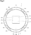
- FIGS. 3 and 4 are diagrams illustrating a state in which the holding member 22 is positioned in the housing 10.
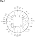
- FIG. 5 is an enlarged plan view illustrating a state in which the frame plate portion 27 is biasing the electron emission plate 21.
- FIG. 6 is an enlarged end view of the holding member 22.
- the first positioning portion 23 and the second positioning portion 24 position the holding member 22 inside the housing 10.
- the first positioning portion 23 has a flat plate portion 23b in which an opening 23a is formed and a plurality of springs 23c.
- the second positioning portion 24 has a flat plate portion 24b in which an opening 24a is formed and a plurality of springs 24c.
- the opening 23a and the opening 24a form a penetration opening 22a of the holding member 22.
- the opening 23a and the opening 24a have rectangular or circular shapes. In the present embodiment, the opening 23a and the opening 24a have rectangular shapes.
- the flat plate portion 23b and the flat plate portion 24b are in contact with each other. When viewed from a direction orthogonal to the main surfaces 21a and 21b of the electron emission plate 21, the emission surface 21d of the electron emission plate 21 is disposed inside an edge that defines the opening 23a and the opening 24a.
- the plurality of springs 23c extends in different directions from each other.
- the plurality of springs 23c is disposed in a circumferential direction of the holding member 22 so as to be rotationally symmetric when viewed from an axis HA direction of the holding member 22.
- the plurality of springs 24c extends in different directions from each other.
- the plurality of springs 24c is disposed in the circumferential direction of the holding member 22 so as to be rotationally symmetric when viewed from the axis HA direction of the holding member 22.
- the plurality of springs 23c and 24c is disposed at equal intervals in the circumferential direction of the pipe shaft TA along the side surface 10a of the housing 10, respectively.
- the plurality of springs 24c is disposed on the window 11a side of the plurality of springs 23c when viewed from a direction orthogonal to the axis HA of the holding member 22.
- the first positioning portion 23 and the second positioning portion 24 have four springs 23c and four springs 24c, respectively.
- the first positioning portion 23 and the second positioning portion 24 position the holding member 22 with respect to the housing 10 by the plurality of springs 23c and the plurality of springs 24c.
- Each spring 23c of the first positioning portion 23 extends in the direction of the axis HA of the holding member 22 and in the direction orthogonal to the axis HA.
- Each spring 23c abuts on the side surface 10a of the housing 10 at a tip and applies an biasing force F1.
- the first positioning portion 23 prevents the holding member 22 from moving in the pipe shaft TA direction of the housing 10 due to a frictional force between the plurality of springs 23c and the side surface 10a of the housing 10.
- Each spring 24c of the second positioning portion 24 extends in an opposite direction to a direction in which the plurality of springs 23c extends when viewed from a direction orthogonal to the axis HA of the holding member 22.
- Each spring 24c has a T-shape, and a tip thereof is divided into two parts. The tips of the each spring 24c are separated in directions opposite from each other in the circumferential direction of the holding member 22 when viewed from the axis HA direction of the holding member 22.
- Each spring 24c abuts on the side surface 10a of the housing 10 at two tips and applies an biasing force F2.
- Each spring 24c elastically holds the position of the holding member 22 inside the housing 10 in the direction orthogonal to the pipe shaft TA of the housing 10.
- the base portion 25 has a flat plate portion 25b in which an opening 25a is formed.
- the base portion 25 is in contact with the main surface 21a of the electron emission plate 21 at the flat plate portion 25b.
- the opening 25a forms a penetration opening 22a of the holding member 22.
- the base portion 25 is in contact with the main surface 21a of the electron emission plate 21 at an edge defining the opening 25a.
- the incident surface 21c of the electron emission plate 21 is disposed inside the edge defining the opening 25a.
- the opening 25a has a rectangular or circular shape. In the present embodiment, the opening 25a has a rectangular shape.
- the base portion 25 has a U-shape in a cross section passing through the axis HA of the holding member 22, and further has a frame 25c extending from a peripheral edge of the flat plate portion 25b to the opposite side from the spacer 26 side in the axis HA direction of the holding member 22.
- the spacer 26 is interposed between the base portion 25 and the frame plate portion 27.
- the spacer 26 has a flat plate portion 26b in which the opening 26a is formed.
- the opening 26a forms a penetration opening 22a of the holding member 22.
- the opening 26a of the spacer 26 has a shape along an edge of the electron emission plate 21. That is, the spacer 26 surrounds the edge of the electron emission plate 21.
- the opening 26a has a rectangular or circular shape. In the present embodiment, the opening 26a has a rectangular shape. The edge of the opening 26a is in contact with the edge of the electron emission plate 21.
- the spacer 26 positions the electron emission plate 21 with respect to the holding member 22 in a direction orthogonal to the axis HA of the holding member 22.
- a thickness T1 of the spacer 26 is equal to or less than a thickness T2 of the electron emission plate. In the present embodiment, the thickness T1 of the spacer 26 is smaller than the thickness T2 of the electron emission plate.
- the frame plate portion 27 is formed of a single plate.
- An opening 27a is formed in the frame plate portion 27.
- the opening 27a forms the penetration opening 22a of the holding member 22.
- the frame plate portion 27 has a flat plate portion 27b and a plurality of biasing portions 27c (electron emission plate biasing portions).
- the flat plate portion 27b and the plurality of biasing portions 27c are integrally formed.
- the flat plate portion 27b is in contact with the spacer 26, and each biasing portion 27c is in contact with the electron emission plate 21.
- the flat plate portion 27b interposes the spacer 26 between the flat plate portion 27b and the base portion 25.
- the opening 27a is defined by the flat plate portion 27b and the plurality of biasing portions 27c. As illustrated in FIG. 5 , when viewed from a direction orthogonal to the main surfaces 21a and 21b of the electron emission plate 21, the emission surface 21d of the electron emission plate 21 is disposed inside the edge defining the opening 27a.
- Each biasing portion 27c is in contact with the edge of the main surface 21b of the electron emission plate 21. Each biasing portion 27c elastically biases the electron emission plate 21 with respect to the flat plate portion 25b of the base portion 25 by applying an biasing force F3 to the edge of the main surface 21b. Each biasing portion 27c is electrically connected to the main surface 21b. That is, the holding member 22 is electrically connected to the main surface 21b through the plurality of biasing portions 27c. The electron emission plate 21 is electrically connected to the wire 13 connected to the holding member 22 through the plurality of biasing portions 27c.
- the plurality of biasing portions 27c is disposed at different positions in the circumferential direction of the edge of the opening 27a, and projects in directions facing each other.
- Each biasing portion 27c projects from the flat plate portion 27b toward the axis HA of the holding member 22 in a direction orthogonal to the axis.
- each biasing portion 27c extends from the flat plate portion 27b to a center side of the opening 27a (the shaft HA side of the holding member 22).
- the plurality of biasing portions 27c is disposed so as to be rotationally symmetric when viewed from the axis HA direction of the holding member 22.
- each biasing portion 27c has a plate shape and functions as a leaf spring that biases the electron emission plate 21 to the base portion 25.
- Each biasing portion 27c is formed flush with the flat plate portion 27b in a state before being in contact with the electron emission plate 21. As illustrated in FIG. 6 , each biasing portion 27c is elastically deformed by coming into contact with the edge of the main surface 21b of the electron emission plate 21, and the biasing force F3 is applied to the main surface 21b of the electron emission plate 21.
- a thickness T3 of each biasing portion 27c is smaller than the thickness T2 of the electron emission plate 21.
- the thickness T3 of each biasing portion 27c is smaller than the thickness T1 of the spacer 26.
- the thicknesses T3 of the flat plate portion 25b and each biasing portion 27c are the same. Note that "same” includes a range of manufacturing tolerance.
- the plurality of biasing portions 27c has a shape in which a plurality of notch-shaped gaps 27d are provided in a radial direction of the holding member 22 (direction orthogonal to the axis HA of the holding member 22) at an edge of a rectangular opening located at a center of the frame plate portion 27.
- the plurality of biasing portions 27c has a shape in which notch-shaped gaps 27d are provided at the four corners of the edge of the rectangular opening.
- each of the plurality of biasing portions 27c is provided on one of sides of the edge of the rectangular opening.
- each biasing portion 27c has a shape in which a plurality of notch-shaped gaps 27e is provided on the above-mentioned side. That is, each biasing portion 27c is divided into a plurality of parts 27f by the gap 27e. Each of the plurality of parts 27f is a metal piece that elastically biases the electron emission plate 21 to the base portion 25. In the present embodiment, each biasing portion 27c is divided into three rectangular parts 27f in a plan view. Each biasing portion 27c may be divided into two parts or may be divided into four or more parts.
- a voltage is applied to the holding member 22, the dynodes 32a to 32j, and the anode 41, respectively, through the wires 13.
- a voltage is applied to the electron emission plate 21 through the frame plate portion 27 of the holding member 22.
- the voltage applied to each of the holding member 22, the dynodes 32a to 32j, and the anode 41 is set so as to gradually increase as the holding member 22 approaches the anode 41.
- the electromagnetic wave passes through the window 11a of the housing 10, and then the electromagnetic wave enters the opening 25a of the base portion 25 of the holding member 22.
- the electromagnetic wave passing through the opening 25a is incident on the incident surface 21c of the electron emission plate 21.
- the electron emission plate 21 emits electrons from the emission surface 21d in response to an incident of an electromagnetic wave.
- the electrons emitted from the electron emission plate 21 pass through the opening 27a of the frame plate portion 27, the opening 24a of the second positioning portion 24, and the opening 23a of the first positioning portion 23 in this order, and then are guided to the incident surface 35 of the electron multiplying unit 30.
- the electrons emitted from the electron emission plate 21 are converged by the focusing electrode 31 and sent to a first-stage dynode 32a (incident surface 35).
- first-stage dynode 32a incident surface 35
- secondary electrons are emitted from the dynode 32a toward the second-stage dynode 32b.
- second-stage dynode 32b secondary electrons are emitted from the dynode 32b toward the third-stage dynode 32c. In this way, electrons are sequentially transmitted from the first-stage dynode 32a to the tenth-stage dynode 32j while being multiplied.
- the electrons emitted from the electron emission plate 21 are cascade-multipliered by the electron multiplying unit 30.
- the electrons multiplied by the electron multiplying unit 30 are collected by the anode 41, which is the electron collecting unit 40, and are output as an output signal from the anode 41 through the wires 13.
- FIG. 7 is an enlarged plan view illustrating a state in which the frame plate portion 27 is biasing the electron emission plate 21 in the electron tube 1 according to the modification.
- the modification illustrated in FIG. 7 is generally similar to or the same as the above-described embodiment. However, the modification is different from the above-described embodiment in that an electron emission plate 21A is held by a holding member 22 instead of the electron emission plate 21.
- a difference between the above-described embodiment and the modification will be mainly described.
- the electron emitting unit 20 has the electron emission plate 21A that emits electrons in response to an incident of an electromagnetic wave, and the holding member 22 that holds the electron emission plate 21A.
- the electron emission plate 21A has a main surface 21a and a main surface 21b facing each other.
- the main surface 21a faces the window 11a.
- the main surface 21a includes an incident surface 21c on which an electromagnetic wave having passed through the window 11a is incident.
- the main surface 21b includes an emission surface 21d that emits electrons.
- the electron emission plate 21A has a metasurface 50 and a substrate 51 provided with the metasurface 50.
- the substrate 51 has an electromagnetic wave transmitting property against an electromagnetic wave transmitted through the window 11a. That is, the substrate 51 transmits at least a part of the frequency band of the electromagnetic wave transmitted through the window 11a.
- the substrate 51 is made of, for example, silicon.
- the substrate 51 has a rectangular shape in a plan view. In this embodiment, the substrate 51 is separated from the window 11a and the electron multiplying unit 30.
- the substrate 51 has a main surface 21a and a main surface 21b facing each other, similarly to the electron emission plate 21.
- the main surface 21a is included in the first main surface
- the main surface 21b is included in the second main surface.
- the main surface 21a and the main surface 21b are disposed parallel to the window 11a.
- the main surface 21a faces the window 11a.
- the main surface 21a includes the incident surface 21c on which an electromagnetic wave having passed through the window 11a is incident.
- the metasurface 50 is provided on the main surface 21b.
- the metasurface 50 emits electrons in response to an incident of an electromagnetic wave. That is, the metasurface 50 includes the emission surface 21d that emits electrons.
- the metasurface 50 when viewed from a direction orthogonal to the main surfaces 21a and 21b of the electron emission plate 21, the metasurface 50 is disposed inside the edge defining the opening 27a of the frame plate portion 27. In this way, when viewed from a direction orthogonal to the main surfaces 21a and 21b of the electron emission plate 21, the incident surface 21c and the emission surface 21d of the electron emission plate 21 are disposed inside the edge defining the penetration opening 22a of the holding member 22.
- the metasurface 50 is included in a patterned oxide layer or patterned metal layer on the main surface 21b of the substrate 51.
- the oxide layer is, for example, titanium oxide.
- the metal layer is, for example, gold.
- the metasurface 50 has a rectangular shape in a plan view. In the present embodiment, the metal layers included in the metasurface 50 form a plurality of antennas on the main surface 21b.
- the metasurface 50 can correspond to a frequency band of about 0.01 to 50 THz, that is, a frequency band of so-called millimeter wave to mid-infrared light. That is, the metasurface 50 can correspond to a frequency band including a so-called terahertz wave.
- the electromagnetic wave passes through the window 11a of the housing 10, and then the electromagnetic wave enters the opening 25a of the base portion 25 of the holding member 22.
- the electromagnetic wave passing through the opening 25a is incident on the incident surface 21c of the substrate 51.
- the electromagnetic wave incident on the incident surface 21c passes through the substrate 51 and is incident on the metasurface 50 provided on the main surface 21b of the substrate 51.
- the metasurface 50 emits electrons in response to the incident of electromagnetic wave.
- the electrons emitted from the metasurface 50 pass through the opening 27a of the frame plate portion 27, the opening 24a of the second positioning portion 24, and the opening 23a of the first positioning portion 23 in this order, and then are guided to the incident surface 35 of the electron multiplying unit 30.
- the plurality of biasing portions 27c of the holding member 22 elastically bias the electron emission plate 21 to the base portion 25. Therefore, even when there is some manufacturing error or deformation by a temperature change in each member of the electron tube 1, the plurality of biasing portions 27c are in stable contact with the electron emission plate 21.
- the holding member 22 is electrically connected to the main surface 21b of the electron emission plate 21 through the plurality of biasing portions 27c. Therefore, the stability of the voltage applied to the main surface 21b of the electron emission plate 21 through the plurality of biasing portions 27c of the holding member 22 is improved.
- the plurality of biasing portions 27c is disposed at positions that are rotationally symmetric when viewed from the normal direction of the main surface 21b. In this case, the biasing force F3 is evenly applied to the electron emission plate 21 by the plurality of biasing portions 27c. Therefore, the electron emission plate 21 is in stable contact with the plurality of biasing portions 27c.
- each biasing portion 27c is smaller than the thickness T2 of the electron emission plate 21. Therefore, the biasing force F3 applied to the electron emission plate 21 from each biasing portion 27c is reduced. Therefore, the damage of the electron emission plate 21 is suppressed.
- Each biasing portion 27c is divided into the plurality of parts 27f.
- Each of the plurality of parts 27f elastically biases the electron emission plate 21 to the base portion 25. Therefore, the biasing force from each biasing portion 27c is more stably applied to the electron emission plate 21. Therefore, the electron emission plate 21 comes into contact with the plurality of biasing portions 27c more stably.
- the flat plate portion 27b is integrally formed with the plurality of biasing portions 27c.
- the spacer 26 is interposed between the base portion 25 and the flat plate portion 27b and surrounds the edge of the electron emission plate 21.
- the plurality of biasing portions 27c projects from the flat plate portion 27b and elastically biases the electron emission plate 21 with respect to the base portion 25.
- the thickness T1 of the spacer 26 is equal to or less than the thickness T2 of the electron emission plate 21.
- the spacer 26 surrounding the edge of the electron emission plate 21 more reliably holds the electron emission plate 21 in a direction orthogonal to a thickness direction of the electron emission plate 21. Since the thickness T1 of the spacer 26 is equal to or less than the thickness T2 of the electron emission plate 21, the biasing force F3 applied to the electron emission plate 21 in the thickness direction of the electron emission plate 21 by the plurality of biasing portions 27c is stably ensured in the state illustrated in FIG. 6 . Therefore, the electron emission plate 21 is more reliably held in the thickness direction of the electron emission plate 21.
- the base portion 25 is in contact with the main surface 21a at an edge defining the opening 25a.
- the electron emission plate 21 can be held more stably, and an electromagnetic wave can be incident on the electron emission plate 21.
- the electron emission plate 21 is a field assist type photocathode. In this case, an electric field is formed on the electron emission plate 21, and electrons are emitted from the main surface 21b of the electron emission plate 21 by the electric field. Therefore, the electron emission plate 21 emits electrons from the main surface 21b in response to an incident of an electromagnetic wave having a frequency band from infrared light to ultraviolet light, for example.
- the electron emission plate 21 has a metasurface 50 that emits electrons in response to an incident of an electromagnetic wave.
- the electron emission plate 21 emits electrons from the metasurface 50 in response to the incident of the electromagnetic wave in a frequency band from millimeter waves to infrared light, for example.
- the plurality of springs 23c and 24c of the holding member 22 positions the holding member 22 with respect to the housing 10 by applying biasing forces F1 and F2 to the inner side surface 10a of the housing 10. In this case, the holding member 22 is stably held with respect to the housing 10 even when there is some manufacturing error or deformation by a temperature change in each member of the electron tube 1.
- the electron tube 1 is a photomultiplier tube.
- the electron tube 1 may be a so-called image intensifier, a streak tube, an image pickup device, etc.
- the holding member 22 positions the electron emission plate 21 with respect to the housing 10 so that the main surface 21a of the electron emission plate 21 faces the window 11a of the housing 10.
- each biasing portion 27c may be formed as one metal piece.
- each biasing portion 27c may be one metal piece having a rectangular shape in a plan view.
- the housing 10 is not limited to the cylindrical shape.
- the housing 10 may have a tubular shape having a polygonal cross section.
- the holding member 22 has the frame plate portion 27.
- the plurality of biasing portions 27c extends from the edge of the flat plate portion 25b of the base portion 25.
- the plurality of biasing portions 27c may extend from the edge of the flat plate portion 25b of the base portion 25 to the main surface 21b side of the electron emission plate 21 and then bend in a direction parallel to the main surface 21b.
- the plurality of biasing portions 27c is in contact with the edge of the main surface 21b, and the electron emission plate 21 is elastically biasd to the flat plate portion 25b of the base portion 25.
Landscapes
- Physics & Mathematics (AREA)
- Electromagnetism (AREA)
- Electron Tubes For Measurement (AREA)
- Image-Pickup Tubes, Image-Amplification Tubes, And Storage Tubes (AREA)
- Photometry And Measurement Of Optical Pulse Characteristics (AREA)
- Common Detailed Techniques For Electron Tubes Or Discharge Tubes (AREA)
Abstract
Description
- The present invention relates to an electron tube.
- A known electron tube holds an electron emission plate in a housing (for example, Patent Literature 1). The electron emission plate emits electrons in response to an incident of an electromagnetic wave. Patent Literature 1 describes an electron tube in which a photocathode plate is held in a housing.
- Patent Literature 1:
Japanese Unexamined Patent Publication No. 2002-42636 - In the electron tube described in Patent Literature 1, the photocathode plate is held by interposing the photocathode plate between a support plate and an incident window. A voltage is applied to the photocathode plate through the support plate. In this configuration, there is concern that a positional relationship between the support plate and the photocathode plate may not be stable due to a manufacturing error and deformation by a temperature change in each member of the electron tube. When the positional relationship between the support plate and the photocathode plate is not stable, there is concern that a voltage applied to the photocathode plate through the support plate may become unstable. Therefore, it is required to apply a stable voltage to the electron emission plate such as the photocathode plate even when there is the manufacturing error and deformation due to the temperature change.
- An object of one aspect of the present invention is to provide an electron tube having an electron emission plate that emits electrons in response to an incident of an electromagnetic wave and having improved stability of a voltage applied to the electron emission plate.
- An electron tube according to an aspect of the present invention includes a housing, an electron emission plate, and a holding member. The housing has a window having an electromagnetic wave transmitting property. The electron emission plate is disposed inside the housing and emits electrons in response to an incident of the electromagnetic wave. The holding member is disposed inside the housing to hold the electron emission plate. The holding member is configured to apply a voltage to the electron emission plate. The electron emission plate has a first main surface and a second main surface facing each other. The holding member has a base portion being in contact with the first main surface, and a plurality of electron emission plate biasing portions. The plurality of electron emission plate biasing portions are in contact with an edge of the second main surface and are configured to elastically bias the electron emission plate to the base portion. The holding member is electrically connected to the second main surface through the plurality of electron emission plate biasing portions.
- In the aspect, the plurality of electron emission plate biasing portions elastically bias the electron emission plate to the base portion (hereinafter, the electron emission plate biasing portion is simply referred to as an "biasing portion"). Therefore, even when there are some manufacturing error and deformation by a temperature in each member of the electron tube, the plurality of biasing portions are in stable contact with the electron emission plate. The holding member is electrically connected to the second main surface of the electron emission plate through the plurality of biasing portions. Therefore, the stability of the voltage applied to the second main surface of the electron emission plate through the plurality of biasing portions of the holding member is improved.
- In the aspect, the plurality of biasing portions may be disposed at rotationally symmetric positions when viewed from the normal direction of the second main surface. In this case, the biasing force is evenly applied to the electron emission plate by the plurality of biasing portions. Therefore, the electron emission plate is in stable contact with the plurality of biasing portions.
- In the aspect, the plurality of biasing portions may have a plate shape. The thickness of each biasing portion may be smaller than the thickness of the electron emission plate. In this case, the biasing force applied to the electron emission plate from each biasing portion is reduced. Therefore, the breakage of the electron emission plate is suppressed.
- In the aspect, each biasing portion may be divided into a plurality of parts. Each of the plurality of parts may elastically bias the electron emission plate to the base portion. In this case, the biasing force from each biasing portion is more stably applied to the electron emission plate. Therefore, the electron emission plate is more stably in contact with the plurality of biasing portions.
- In the aspect, the holding member may have a frame plate portion and a spacer. The frame plate portion may include a plurality of electron emission plate biasing portions and a flat plate portion integrally formed with the plurality of electron emission plate biasing portions. The spacer may be interposed between the base portion and the flat plate portion, and surround the edge of the electron emission plate. The plurality of biasing portions may project from the flat plate portion, and elastically bias the electron emission plate to the base portion. A thickness of the spacer may be less than or equal to a thickness of the electron emission plate. In this case, the spacer surrounding the edge of the electron emission plate more reliably holds the electron emission plate in the direction orthogonal to the thickness direction of the electron emission plate. Since the thickness of the spacer is less than or equal to the thickness of the electron emission plate, an biasing force applied to the electron emission plate in the thickness direction of the electron emission plate by the plurality of biasing portions is stably ensured. Therefore, the electron emission plate is more reliably held in the thickness direction of the electron emission plate.
- In the aspect, an opening may be formed in the frame plate portion. This opening is defined by the plurality of electron emission plate biasing portions and the flat plate portion. The plurality of electron emission plate biasing portions may extend from the flat plate portion to the center side of the opening in directions facing each other.
- In the aspect, an opening may be formed in the base portion. An electromagnetic wave having passed through the window enters this opening. This opening may have a rectangular shape or a circular shape. The base portion may be in contact with the first main surface at the edge defining the opening. In this case, the electron emission plate is held more stably, and the electromagnetic wave can be incident on the electron emission plate.
- In the aspect, the electron emission plate may be a field assist type photocathode. In this case, an electric field is formed in the electron emission plate, and the electric field emits electrons from the second main surface of the electron emission plate. Therefore, the electron emission plate emits electrons from the second main surface in response to an incident of an electromagnetic wave having a frequency band from infrared light to ultraviolet light, for example.
- In the aspect, the electron emission plate may have a metasurface configured to emits electrons in response to an incident of an electromagnetic wave. In this case, the electron emission plate emits electrons from the metasurface in response to the incident of electromagnetic wave in the frequency band from millimeter waves to infrared light, for example.
- In the aspect, the housing may have a tubular shape. The holding member may have a plurality of springs configured to position the holding member with respect to the housing by applying an biasing force to the inner side surface of the housing. In this case, the holding member is stably held with respect to the housing even when there is some manufacturing error or deformation by a temperature change in each member of the electron tube.
- One aspect of the present invention provides an electron tube capable of stably applying a voltage to an electron emission plate configured to emit electrons in response to an incident of an electromagnetic wave.
-
-
FIG. 1 is a cross-sectional view illustrating an electron tube according to an embodiment. -
FIG. 2 is an exploded perspective view of a holding member. -
FIG. 3 is a diagram illustrating a state in which the holding member is positioned in a housing. -
FIG. 4 is a diagram illustrating a state in which the holding member is positioned in the housing. -
FIG. 5 is an enlarged plan view illustrating a state in which a frame plate portion biases an electron emission plate. -
FIG. 6 is an enlarged end view of the holding member. -
FIG. 7 is an enlarged plan view illustrating a state in which a frame plate portion biases an electron emission plate in an electron tube according to a modification of the present embodiment. - Hereinafter, an embodiment of the present invention will be described in detail with reference to the accompanying drawings. Note that in the description, the same reference symbol will be used for the same element or an element having the same function, and duplicate description will be omitted.
- First, a configuration of an electron tube according to the present embodiment will be described with reference to
FIGS. 1 and2 .FIG. 1 is a cross-sectional view illustrating an example of the electron tube. - An electron tube 1 is a photomultiplier tube that outputs an electric signal in response to an incident of an electromagnetic wave. In the present specification, an "electromagnetic wave" entering the electron tube is an electromagnetic wave having a frequency band of so-called millimeter wave to ultraviolet light. The electron tube 1 emits electrons and multipliers the emitted electrons, when an electromagnetic wave enters the electron tube 1. In the present embodiment, the electron tube 1 causes an electromagnetic wave to enter a photoelectric surface and multiplies the electrons emitted from the photoelectric surface by the external photoelectric effect. As illustrated in
FIG. 1 , the electron tube 1 includes ahousing 10, anelectron emitting unit 20, anelectron multiplying unit 30, and anelectron collecting unit 40. - The
housing 10 has avalve 11 and astem 12. The inside of thehousing 10 is held in a vacuum by being hermetically sealed by thevalve 11 and thestem 12. The vacuum includes not only an absolute vacuum but also a state filled with a gas having a pressure lower than the atmospheric pressure. For example, the inside of thehousing 10 is held at 1 × 10⁻⁴ to 1 × 10⁻⁷ Pa. Thevalve 11 has awindow 11a having an electromagnetic wave transmitting property. In the present specification, the term "electromagnetic wave transmitting property" refers to a property that at least a part of a frequency band of an incident electromagnetic wave is transmitted. In the present embodiment, thehousing 10 has a cylindrical shape. Thestem 12 is included in a bottom surface of thehousing 10. Thevalve 11 is included in a side surface of thehousing 10 and a bottom surface facing thestem 12. - The
window 11a is included in the bottom surface facing thestem 12. Thewindow 11a has, for example, a circular shape in a plan view. A frequency characteristic of a transmittance of an electromagnetic wave differs depending on the material. Therefore, thewindow 11a is made of an optimum material according to the frequency band of the electromagnetic wave entering the electron tube 1. For example, thewindow 11a includes, for example, at least one type selected from quartz, silicon, germanium, sapphire, zinc selenide, zinc sulfide, magnesium fluoride, lithium fluoride, barium fluoride, calcium fluoride, magnesium oxide, calcium carbonate, UV glass, and borosilicate glass. By constructing thewindow 11a using a material selected from these materials, an electromagnetic wave in any frequency band from millimeter waves to ultraviolet light can be guided to the inside of thehousing 10. - The electron tube 1 further has a plurality of
wires 13 that allows electric connection between the outside and the inside of thehousing 10. The plurality ofwires 13 is, for example, lead wires or pins. In the present embodiment, the plurality ofwires 13 is pins penetrating thestem 12 and extends from the inside to the outside of thehousing 10. At least one of the plurality ofwires 13 is connected to various members provided inside thehousing 10. - The
electron emitting unit 20 is disposed inside thehousing 10, and emits electrons inside thehousing 10 in response to the incident of the electromagnetic wave. Theelectron emitting unit 20 has anelectron emission plate 21 that emits electrons in response to the incident of the electromagnetic wave, and a holdingmember 22 that holds theelectron emission plate 21. The holdingmember 22 applies a voltage to theelectron emission plate 21. - The
electron emission plate 21 has amain surface 21a and amain surface 21b facing each other. For example, when themain surface 21a is included in a first main surface, themain surface 21b is included in a second main surface. Themain surface 21a and themain surface 21b are disposed parallel to thewindow 11a. Themain surface 21a faces thewindow 11a. Themain surface 21a includes anincident surface 21c on which an electromagnetic wave having passed through thewindow 11a is incident. Themain surface 21b includes anemission surface 21d that emits electrons. - In the present embodiment, the
electron emission plate 21 is a field assist type photocathode. In the present embodiment, theelectron emission plate 21 emits electrons by the external photoelectric effect when an electromagnetic wave is incident. In the present embodiment, theelectron emission plate 21 emits electrons in response to an incident of an electromagnetic wave having a frequency band from infrared light to ultraviolet light, for example. For example, theelectron emission plate 21 has, as theemission surface 21d, a photoelectric surface containing Cs-I, Cs-Te, Sb-Cs, bialkali (Sb-Rb-Cs, Sb-K-Cs, and Sb-Na-K), multi-alkali (Sb-Na-K-Cs), Ag-O-Cs, GaAsP (Cs), GaAs (Cs), InGaAs (Cs), InP/InGaAsP (Cs), InP/InGaAs (Cs), etc. - The holding
member 22 is positioned with respect to aninner side surface 10a of thehousing 10. That is, the holdingmember 22 positions theelectron emission plate 21 with respect to thehousing 10. The holdingmember 22 has a frame shape along theside surface 10a of thehousing 10. Apenetration opening 22a is formed in the holdingmember 22. When viewed from a direction orthogonal to themain surfaces electron emission plate 21, theincident surface 21c and theemission surface 21d of theelectron emission plate 21 are disposed inside an edge defining thepenetration opening 22a. In a state in which the holdingmember 22 is positioned with respect to thehousing 10, a pipe shaft TA of thehousing 10 passes through thepenetration opening 22a. The holdingmember 22 is positioned with respect to thehousing 10 so that an optical axis of the electromagnetic wave passing through thepenetration opening 22a (hereinafter, referred to as an "axis of the holdingmember 22") is parallel to the pipe shaft TA of thehousing 10. The axis HA of the holdingmember 22 is orthogonal to themain surfaces electron emission plate 21. The holdingmember 22 is connected to at least one of the plurality ofwires 13. -
FIG. 2 is an exploded perspective view of the holdingmember 22. The holdingmember 22 has afirst positioning portion 23, asecond positioning portion 24, abase portion 25, aspacer 26, and aframe plate portion 27. Thefirst positioning portion 23, thesecond positioning portion 24, thebase portion 25, thespacer 26, and theframe plate portion 27 are welded to each other while holding theelectron emission plate 21. In a state where the holdingmember 22 is positioned in thehousing 10, thebase portion 25, thespacer 26, theframe plate portion 27, thesecond positioning portion 24, and thefirst positioning portion 23 are located in this order from thewindow 11a side. Each of thefirst positioning portion 23, thesecond positioning portion 24, thebase portion 25, thespacer 26, and theframe plate portion 27 has conductivity. At least theframe plate portion 27 is electrically connected to thewire 13. - The
electron multiplying unit 30 is disposed inside thehousing 10 and has anincident surface 35 on which the electrons emitted from theelectron emitting unit 20 are incident. Theelectron multiplying unit 30 multiplies the electrons incident on theincident surface 35. In the present embodiment, themain surface 21b of theelectron emission plate 21 faces theincident surface 35 of theelectron multiplying unit 30. That is, theemission surface 21d of theelectron emission plate 21 faces theincident surface 35 of theelectron multiplying unit 30, and the electrons emitted from theemission surface 21d are incident on theincident surface 35. Themain surface 21a of theelectron emission plate 21 faces thewindow 11a of thehousing 10. - In the present specification, an expression "α faces β" means that β is located in a normal direction of α with respect to a plane tangent to α. In other words, the expression "α faces β" means that when a space is divided into two parts by a surface in contact with α, β is located on the α side, not on the back side of α. For example, in the electron tube 1, as described above, the
emission surface 21d of theelectron emission plate 21 faces theincident surface 35 of theelectron multiplying unit 30, which means that theincident surface 35 of theelectron multiplying unit 30 is located in the normal direction of theemission surface 21d with respect to a plane in contact with theemission surface 21d. - In the present embodiment, as illustrated in
FIG. 1 , theelectron multiplying unit 30 has a so-called line focus type multi-stage dynode. In the present embodiment, theelectron multiplying unit 30 has a focusingelectrode 31 for focusing electrons and a plurality of stages ofdynodes dynode 32a includes theincident surface 35 described above. In the present embodiment, theelectron multiplying unit 30 has ten stages ofdynodes 32a to 32j. A circular incident opening 31a is provided at a center of the focusingelectrode 31. Thedynodes 32a to 32j are disposed after theincident opening 31a. One of the plurality ofwires 13 is connected to each of thedynodes 32a to 32j. A predetermined potential is applied to each of thedynodes 32a to 32j through thewires 13. Thedynodes 32a to 32j multiply the electrons having passed through theincident opening 31a according to the applied potential. - The
electron collecting unit 40 is disposed inside thehousing 10, and collects the electrons multiplied by theelectron multiplying unit 30. In the present embodiment, theelectron collecting unit 40 has a mesh-shapedanode 41. Theanode 41 faces themain surface 21b of theelectron emission plate 21. One of the plurality ofwires 13 is connected to theanode 41. A predetermined potential is applied to theanode 41 through thewires 13. Theanode 41 captures the electrons multiplied by thedynodes 32a to 32j. Theelectron collecting unit 40 may have a diode instead of theanode 41. - In the present embodiment, the electron tube 1 has a pair of insulating
substrates 52 for fixing thedynodes 32a to 32j and theanode 41 inside thehousing 10. The pair of insulatingsubstrates 52 is made of alumina. The pair of insulatingsubstrates 52 faces each other. Thedynodes 32a to 32j have a pair of ends extending in opposite directions of the pair of insulatingsubstrates 52. Theanode 41 has a pair of ends extending in the opposite directions of the pair of insulatingsubstrates 52. Each end of thedynodes 32a to 32j and theanode 41 is inserted into a slit-shaped through-hole provided in advance in the pair of insulatingsubstrates 52. - The electron tube 1 has a shielding
plate 36 that partially surrounds thedynodes 32a to 32j and theanode 41. The shieldingplate 36 prevents light and ions generated by the collision of electrons multiplied by thedynodes 32a to 32j from scattering inside thehousing 10. The shieldingplate 36 is connected to one of the plurality ofwires 13. A predetermined potential is applied to the shieldingplate 36 through thewires 13. - Next, a configuration of the holding
member 22 in theelectron emitting unit 20 will be described in detail with reference toFIGS. 3 to 6 .FIGS. 3 and4 are diagrams illustrating a state in which the holdingmember 22 is positioned in thehousing 10.FIG. 5 is an enlarged plan view illustrating a state in which theframe plate portion 27 is biasing theelectron emission plate 21.FIG. 6 is an enlarged end view of the holdingmember 22. - As illustrated in
FIGS. 3 and4 , thefirst positioning portion 23 and thesecond positioning portion 24 position the holdingmember 22 inside thehousing 10. Thefirst positioning portion 23 has aflat plate portion 23b in which anopening 23a is formed and a plurality ofsprings 23c. Thesecond positioning portion 24 has aflat plate portion 24b in which anopening 24a is formed and a plurality ofsprings 24c. Theopening 23a and theopening 24a form apenetration opening 22a of the holdingmember 22. Theopening 23a and theopening 24a have rectangular or circular shapes. In the present embodiment, theopening 23a and theopening 24a have rectangular shapes. Theflat plate portion 23b and theflat plate portion 24b are in contact with each other. When viewed from a direction orthogonal to themain surfaces electron emission plate 21, theemission surface 21d of theelectron emission plate 21 is disposed inside an edge that defines theopening 23a and theopening 24a. - The plurality of
springs 23c extends in different directions from each other. In the present embodiment, the plurality ofsprings 23c is disposed in a circumferential direction of the holdingmember 22 so as to be rotationally symmetric when viewed from an axis HA direction of the holdingmember 22. The plurality ofsprings 24c extends in different directions from each other. In the present embodiment, the plurality ofsprings 24c is disposed in the circumferential direction of the holdingmember 22 so as to be rotationally symmetric when viewed from the axis HA direction of the holdingmember 22. - In the present embodiment, the plurality of
springs side surface 10a of thehousing 10, respectively. The plurality ofsprings 24c is disposed on thewindow 11a side of the plurality ofsprings 23c when viewed from a direction orthogonal to the axis HA of the holdingmember 22. In the present embodiment, thefirst positioning portion 23 and thesecond positioning portion 24 have foursprings 23c and foursprings 24c, respectively. - The
first positioning portion 23 and thesecond positioning portion 24 position the holdingmember 22 with respect to thehousing 10 by the plurality ofsprings 23c and the plurality ofsprings 24c. Eachspring 23c of thefirst positioning portion 23 extends in the direction of the axis HA of the holdingmember 22 and in the direction orthogonal to the axis HA. Eachspring 23c abuts on theside surface 10a of thehousing 10 at a tip and applies an biasing force F1. Thefirst positioning portion 23 prevents the holdingmember 22 from moving in the pipe shaft TA direction of thehousing 10 due to a frictional force between the plurality ofsprings 23c and theside surface 10a of thehousing 10. - Each
spring 24c of thesecond positioning portion 24 extends in an opposite direction to a direction in which the plurality ofsprings 23c extends when viewed from a direction orthogonal to the axis HA of the holdingmember 22. Eachspring 24c has a T-shape, and a tip thereof is divided into two parts. The tips of the eachspring 24c are separated in directions opposite from each other in the circumferential direction of the holdingmember 22 when viewed from the axis HA direction of the holdingmember 22. Eachspring 24c abuts on theside surface 10a of thehousing 10 at two tips and applies an biasing force F2. Eachspring 24c elastically holds the position of the holdingmember 22 inside thehousing 10 in the direction orthogonal to the pipe shaft TA of thehousing 10. - The
base portion 25 has aflat plate portion 25b in which anopening 25a is formed. Thebase portion 25 is in contact with themain surface 21a of theelectron emission plate 21 at theflat plate portion 25b. Theopening 25a forms apenetration opening 22a of the holdingmember 22. Thebase portion 25 is in contact with themain surface 21a of theelectron emission plate 21 at an edge defining theopening 25a. When viewed from a direction orthogonal to themain surfaces electron emission plate 21, theincident surface 21c of theelectron emission plate 21 is disposed inside the edge defining theopening 25a. Theopening 25a has a rectangular or circular shape. In the present embodiment, theopening 25a has a rectangular shape. In the present embodiment, thebase portion 25 has a U-shape in a cross section passing through the axis HA of the holdingmember 22, and further has aframe 25c extending from a peripheral edge of theflat plate portion 25b to the opposite side from thespacer 26 side in the axis HA direction of the holdingmember 22. - The
spacer 26 is interposed between thebase portion 25 and theframe plate portion 27. Thespacer 26 has aflat plate portion 26b in which theopening 26a is formed. Theopening 26a forms apenetration opening 22a of the holdingmember 22. Theopening 26a of thespacer 26 has a shape along an edge of theelectron emission plate 21. That is, thespacer 26 surrounds the edge of theelectron emission plate 21. Theopening 26a has a rectangular or circular shape. In the present embodiment, theopening 26a has a rectangular shape. The edge of theopening 26a is in contact with the edge of theelectron emission plate 21. - The
spacer 26 positions theelectron emission plate 21 with respect to the holdingmember 22 in a direction orthogonal to the axis HA of the holdingmember 22. A thickness T1 of thespacer 26 is equal to or less than a thickness T2 of the electron emission plate. In the present embodiment, the thickness T1 of thespacer 26 is smaller than the thickness T2 of the electron emission plate. - The
frame plate portion 27 is formed of a single plate. Anopening 27a is formed in theframe plate portion 27. Theopening 27a forms thepenetration opening 22a of the holdingmember 22. Theframe plate portion 27 has aflat plate portion 27b and a plurality of biasingportions 27c (electron emission plate biasing portions). Theflat plate portion 27b and the plurality of biasingportions 27c are integrally formed. Theflat plate portion 27b is in contact with thespacer 26, and each biasingportion 27c is in contact with theelectron emission plate 21. Theflat plate portion 27b interposes thespacer 26 between theflat plate portion 27b and thebase portion 25. Theopening 27a is defined by theflat plate portion 27b and the plurality of biasingportions 27c. As illustrated inFIG. 5 , when viewed from a direction orthogonal to themain surfaces electron emission plate 21, theemission surface 21d of theelectron emission plate 21 is disposed inside the edge defining theopening 27a. - Each biasing
portion 27c is in contact with the edge of themain surface 21b of theelectron emission plate 21. Each biasingportion 27c elastically biases theelectron emission plate 21 with respect to theflat plate portion 25b of thebase portion 25 by applying an biasing force F3 to the edge of themain surface 21b. Each biasingportion 27c is electrically connected to themain surface 21b. That is, the holdingmember 22 is electrically connected to themain surface 21b through the plurality of biasingportions 27c. Theelectron emission plate 21 is electrically connected to thewire 13 connected to the holdingmember 22 through the plurality of biasingportions 27c. - The plurality of biasing
portions 27c is disposed at different positions in the circumferential direction of the edge of theopening 27a, and projects in directions facing each other. Each biasingportion 27c projects from theflat plate portion 27b toward the axis HA of the holdingmember 22 in a direction orthogonal to the axis. In other words, each biasingportion 27c extends from theflat plate portion 27b to a center side of theopening 27a (the shaft HA side of the holding member 22). In the present embodiment, the plurality of biasingportions 27c is disposed so as to be rotationally symmetric when viewed from the axis HA direction of the holdingmember 22. - In the present embodiment, each biasing
portion 27c has a plate shape and functions as a leaf spring that biases theelectron emission plate 21 to thebase portion 25. Each biasingportion 27c is formed flush with theflat plate portion 27b in a state before being in contact with theelectron emission plate 21. As illustrated inFIG. 6 , each biasingportion 27c is elastically deformed by coming into contact with the edge of themain surface 21b of theelectron emission plate 21, and the biasing force F3 is applied to themain surface 21b of theelectron emission plate 21. A thickness T3 of each biasingportion 27c is smaller than the thickness T2 of theelectron emission plate 21. The thickness T3 of each biasingportion 27c is smaller than the thickness T1 of thespacer 26. The thicknesses T3 of theflat plate portion 25b and each biasingportion 27c are the same. Note that "same" includes a range of manufacturing tolerance. - In the present embodiment, the plurality of biasing
portions 27c has a shape in which a plurality of notch-shapedgaps 27d are provided in a radial direction of the holding member 22 (direction orthogonal to the axis HA of the holding member 22) at an edge of a rectangular opening located at a center of theframe plate portion 27. In the present embodiment, the plurality of biasingportions 27c has a shape in which notch-shapedgaps 27d are provided at the four corners of the edge of the rectangular opening. In the present embodiment, each of the plurality of biasingportions 27c is provided on one of sides of the edge of the rectangular opening. - In the present embodiment, each biasing
portion 27c has a shape in which a plurality of notch-shapedgaps 27e is provided on the above-mentioned side. That is, each biasingportion 27c is divided into a plurality ofparts 27f by thegap 27e. Each of the plurality ofparts 27f is a metal piece that elastically biases theelectron emission plate 21 to thebase portion 25. In the present embodiment, each biasingportion 27c is divided into threerectangular parts 27f in a plan view. Each biasingportion 27c may be divided into two parts or may be divided into four or more parts. - Next, a description will be given of an operation when an electromagnetic wave enters the electron tube 1 in the present embodiment. A voltage is applied to the holding
member 22, thedynodes 32a to 32j, and theanode 41, respectively, through thewires 13. At this time, a voltage is applied to theelectron emission plate 21 through theframe plate portion 27 of the holdingmember 22. The voltage applied to each of the holdingmember 22, thedynodes 32a to 32j, and theanode 41 is set so as to gradually increase as the holdingmember 22 approaches theanode 41. - The electromagnetic wave passes through the
window 11a of thehousing 10, and then the electromagnetic wave enters theopening 25a of thebase portion 25 of the holdingmember 22. The electromagnetic wave passing through theopening 25a is incident on theincident surface 21c of theelectron emission plate 21. Theelectron emission plate 21 emits electrons from theemission surface 21d in response to an incident of an electromagnetic wave. The electrons emitted from theelectron emission plate 21 pass through theopening 27a of theframe plate portion 27, theopening 24a of thesecond positioning portion 24, and theopening 23a of thefirst positioning portion 23 in this order, and then are guided to theincident surface 35 of theelectron multiplying unit 30. - The electrons emitted from the
electron emission plate 21 are converged by the focusingelectrode 31 and sent to a first-stage dynode 32a (incident surface 35). When electrons enter the first-stage dynode 32a (incident surface 35), secondary electrons are emitted from thedynode 32a toward the second-stage dynode 32b. When electrons enter the second-stage dynode 32b, secondary electrons are emitted from thedynode 32b toward the third-stage dynode 32c. In this way, electrons are sequentially transmitted from the first-stage dynode 32a to the tenth-stage dynode 32j while being multiplied. That is, the electrons emitted from theelectron emission plate 21 are cascade-multipliered by theelectron multiplying unit 30. The electrons multiplied by theelectron multiplying unit 30 are collected by theanode 41, which is theelectron collecting unit 40, and are output as an output signal from theanode 41 through thewires 13. - Next, an electron tube according to a modification of the present embodiment will be described with reference to
FIG. 7. FIG. 7 is an enlarged plan view illustrating a state in which theframe plate portion 27 is biasing theelectron emission plate 21 in the electron tube 1 according to the modification. The modification illustrated inFIG. 7 is generally similar to or the same as the above-described embodiment. However, the modification is different from the above-described embodiment in that anelectron emission plate 21A is held by a holdingmember 22 instead of theelectron emission plate 21. Hereinafter, a difference between the above-described embodiment and the modification will be mainly described. - In this modification, the
electron emitting unit 20 has theelectron emission plate 21A that emits electrons in response to an incident of an electromagnetic wave, and the holdingmember 22 that holds theelectron emission plate 21A. Similarly to theelectron emission plate 21, theelectron emission plate 21A has amain surface 21a and amain surface 21b facing each other. Themain surface 21a faces thewindow 11a. Themain surface 21a includes anincident surface 21c on which an electromagnetic wave having passed through thewindow 11a is incident. Themain surface 21b includes anemission surface 21d that emits electrons. - The
electron emission plate 21A has ametasurface 50 and asubstrate 51 provided with themetasurface 50. Thesubstrate 51 has an electromagnetic wave transmitting property against an electromagnetic wave transmitted through thewindow 11a. That is, thesubstrate 51 transmits at least a part of the frequency band of the electromagnetic wave transmitted through thewindow 11a. Thesubstrate 51 is made of, for example, silicon. Thesubstrate 51 has a rectangular shape in a plan view. In this embodiment, thesubstrate 51 is separated from thewindow 11a and theelectron multiplying unit 30. - The
substrate 51 has amain surface 21a and amain surface 21b facing each other, similarly to theelectron emission plate 21. For example, when themain surface 21a is included in the first main surface, themain surface 21b is included in the second main surface. Themain surface 21a and themain surface 21b are disposed parallel to thewindow 11a. Themain surface 21a faces thewindow 11a. Themain surface 21a includes theincident surface 21c on which an electromagnetic wave having passed through thewindow 11a is incident. - The
metasurface 50 is provided on themain surface 21b. Themetasurface 50 emits electrons in response to an incident of an electromagnetic wave. That is, themetasurface 50 includes theemission surface 21d that emits electrons. As illustrated inFIG. 7 , when viewed from a direction orthogonal to themain surfaces electron emission plate 21, themetasurface 50 is disposed inside the edge defining theopening 27a of theframe plate portion 27. In this way, when viewed from a direction orthogonal to themain surfaces electron emission plate 21, theincident surface 21c and theemission surface 21d of theelectron emission plate 21 are disposed inside the edge defining thepenetration opening 22a of the holdingmember 22. - The
metasurface 50 is included in a patterned oxide layer or patterned metal layer on themain surface 21b of thesubstrate 51. The oxide layer is, for example, titanium oxide. The metal layer is, for example, gold. Themetasurface 50 has a rectangular shape in a plan view. In the present embodiment, the metal layers included in themetasurface 50 form a plurality of antennas on themain surface 21b. - The smaller the size of the antennas of the
metasurface 50, the more sensitive it is to an electromagnetic wave having a shorter wavelength, that is, an electromagnetic wave having a higher frequency. By changing the structure of the antennas, themetasurface 50 can correspond to a frequency band of about 0.01 to 50 THz, that is, a frequency band of so-called millimeter wave to mid-infrared light. That is, themetasurface 50 can correspond to a frequency band including a so-called terahertz wave. - Next, a description will be given of an operation when an electromagnetic wave enters the electron tube 1 in this modification. The electromagnetic wave passes through the
window 11a of thehousing 10, and then the electromagnetic wave enters theopening 25a of thebase portion 25 of the holdingmember 22. The electromagnetic wave passing through theopening 25a is incident on theincident surface 21c of thesubstrate 51. The electromagnetic wave incident on theincident surface 21c passes through thesubstrate 51 and is incident on themetasurface 50 provided on themain surface 21b of thesubstrate 51. Themetasurface 50 emits electrons in response to the incident of electromagnetic wave. The electrons emitted from themetasurface 50 pass through theopening 27a of theframe plate portion 27, theopening 24a of thesecond positioning portion 24, and theopening 23a of thefirst positioning portion 23 in this order, and then are guided to theincident surface 35 of theelectron multiplying unit 30. - As described above, in the electron tube 1, the plurality of biasing
portions 27c of the holdingmember 22 elastically bias theelectron emission plate 21 to thebase portion 25. Therefore, even when there is some manufacturing error or deformation by a temperature change in each member of the electron tube 1, the plurality of biasingportions 27c are in stable contact with theelectron emission plate 21. The holdingmember 22 is electrically connected to themain surface 21b of theelectron emission plate 21 through the plurality of biasingportions 27c. Therefore, the stability of the voltage applied to themain surface 21b of theelectron emission plate 21 through the plurality of biasingportions 27c of the holdingmember 22 is improved. - The plurality of biasing
portions 27c is disposed at positions that are rotationally symmetric when viewed from the normal direction of themain surface 21b. In this case, the biasing force F3 is evenly applied to theelectron emission plate 21 by the plurality of biasingportions 27c. Therefore, theelectron emission plate 21 is in stable contact with the plurality of biasingportions 27c. - The thickness T3 of each biasing
portion 27c is smaller than the thickness T2 of theelectron emission plate 21. Therefore, the biasing force F3 applied to theelectron emission plate 21 from each biasingportion 27c is reduced. Therefore, the damage of theelectron emission plate 21 is suppressed. - Each biasing
portion 27c is divided into the plurality ofparts 27f. Each of the plurality ofparts 27f elastically biases theelectron emission plate 21 to thebase portion 25. Therefore, the biasing force from each biasingportion 27c is more stably applied to theelectron emission plate 21. Therefore, theelectron emission plate 21 comes into contact with the plurality of biasingportions 27c more stably. - The
flat plate portion 27b is integrally formed with the plurality of biasingportions 27c. Thespacer 26 is interposed between thebase portion 25 and theflat plate portion 27b and surrounds the edge of theelectron emission plate 21. The plurality of biasingportions 27c projects from theflat plate portion 27b and elastically biases theelectron emission plate 21 with respect to thebase portion 25. The thickness T1 of thespacer 26 is equal to or less than the thickness T2 of theelectron emission plate 21. - In this case, the
spacer 26 surrounding the edge of theelectron emission plate 21 more reliably holds theelectron emission plate 21 in a direction orthogonal to a thickness direction of theelectron emission plate 21. Since the thickness T1 of thespacer 26 is equal to or less than the thickness T2 of theelectron emission plate 21, the biasing force F3 applied to theelectron emission plate 21 in the thickness direction of theelectron emission plate 21 by the plurality of biasingportions 27c is stably ensured in the state illustrated inFIG. 6 . Therefore, theelectron emission plate 21 is more reliably held in the thickness direction of theelectron emission plate 21. - The
base portion 25 is in contact with themain surface 21a at an edge defining theopening 25a. In this case, theelectron emission plate 21 can be held more stably, and an electromagnetic wave can be incident on theelectron emission plate 21. - The
electron emission plate 21 is a field assist type photocathode. In this case, an electric field is formed on theelectron emission plate 21, and electrons are emitted from themain surface 21b of theelectron emission plate 21 by the electric field. Therefore, theelectron emission plate 21 emits electrons from themain surface 21b in response to an incident of an electromagnetic wave having a frequency band from infrared light to ultraviolet light, for example. - The
electron emission plate 21 has ametasurface 50 that emits electrons in response to an incident of an electromagnetic wave. In this case, theelectron emission plate 21 emits electrons from themetasurface 50 in response to the incident of the electromagnetic wave in a frequency band from millimeter waves to infrared light, for example. - The plurality of
springs member 22 positions the holdingmember 22 with respect to thehousing 10 by applying biasing forces F1 and F2 to theinner side surface 10a of thehousing 10. In this case, the holdingmember 22 is stably held with respect to thehousing 10 even when there is some manufacturing error or deformation by a temperature change in each member of the electron tube 1. - Even though the embodiment and modification of the present invention have been described above, the present invention is not necessarily limited to the above-described embodiment and modification, and various modifications can be made without departing from the gist thereof.
- For example, in the present embodiment and modification, a description has been given of a case where the electron tube 1 is a photomultiplier tube. However, the present invention is not limited thereto. The electron tube 1 may be a so-called image intensifier, a streak tube, an image pickup device, etc. In this case as well, the holding
member 22 positions theelectron emission plate 21 with respect to thehousing 10 so that themain surface 21a of theelectron emission plate 21 faces thewindow 11a of thehousing 10. - In the present embodiment and modification, a description has been given of a configuration in which each biasing
portion 27c is divided into the plurality ofparts 27f by thegap 27e. However, each biasingportion 27c may be formed as one metal piece. For example, each biasingportion 27c may be one metal piece having a rectangular shape in a plan view. - The
housing 10 is not limited to the cylindrical shape. For example, thehousing 10 may have a tubular shape having a polygonal cross section. - In the present embodiment, a description has been given of a configuration in which the holding
member 22 has theframe plate portion 27. However, it is possible to adopt a configuration in which the plurality of biasingportions 27c extends from the edge of theflat plate portion 25b of thebase portion 25. In this case, the plurality of biasingportions 27c may extend from the edge of theflat plate portion 25b of thebase portion 25 to themain surface 21b side of theelectron emission plate 21 and then bend in a direction parallel to themain surface 21b. In this case as well, the plurality of biasingportions 27c is in contact with the edge of themain surface 21b, and theelectron emission plate 21 is elastically biasd to theflat plate portion 25b of thebase portion 25. - 1: electron tube, 10: housing, 10a: side surface, 11a: window, 21: electron emission plate, 21a, 21b: main surface, 22: holding member, 23c, 24c: spring, 25: base portion, 25a, 27a: opening, 26: spacer, 27b: flat plate portion, 27c: biasing portion, 27f: part, 50: metasurface, T1, T2, T3: thickness.
Claims (10)
- An electron tube comprising:a housing having a window having an electromagnetic wave transmitting property;an electron emission plate disposed inside the housing, the electron emission plate emitting electrons in response to an incident of the electromagnetic wave; anda holding member disposed inside the housing to hold the electron emission plate and configured to apply a voltage to the electron emission plate,wherein the electron emission plate has a first main surface and a second main surface facing each other, andthe holding member has a base portion being in contact with the first main surface, and a plurality of electron emission plate biasing portions which are in contact with an edge of the second main surface and are configured to elastically bias the electron emission plate to the base portion, and is electrically connected to the second main surface through the plurality of electron emission plate biasing portions.
- The electron tube according to claim 1, wherein the plurality of electron emission plate biasing portions are disposed at rotationally symmetric positions when viewed from a normal direction of the second main surface.
- The electron tube according to claim 1 or 2,wherein the plurality of electron emission plate biasing portions have a plate shape, anda thickness of each of the electron emission plate biasing portions is smaller than a thickness of the electron emission plate.
- The electron tube according to any one of claims 1 to 3,wherein each of the electron emission plate biasing portions is divided into a plurality of parts, andeach of the plurality of parts elastically is configured to bias the electron emission plate to the base portion.
- The electron tube according to any one of claims 1 to 4,wherein the holding member has:a frame plate portion including the plurality of electron emission plate biasing portions and a flat plate portion integrally formed with the plurality of electron emission plate biasing portions, anda spacer which is interposed between the base portion and the flat plate portion and surrounds an edge of the electron emission plate,the plurality of electron emission plate biasing portions project from the flat plate portion and are configured to elastically bias the electron emission plate to the base portion, anda thickness of the spacer is less than or equal to a thickness of the electron emission plate.
- The electron tube according to claim 5,wherein an opening defined by the plurality of electron emission plate biasing portions and the flat plate portion is formed in the frame plate portion, andthe plurality of electron emission plate biasing portions extend from the flat plate portion to a center side of the opening in directions facing each other.
- The electron tube according to any one of claims 1 to 6,wherein an opening which an electromagnetic wave having passed through the window enters is formed in the base portion,the opening has a rectangular shape or a circular shape, andthe base portion is in contact with the first main surface at an edge defining the opening.
- The electron tube according to any one of claims 1 to 7, wherein the electron emission plate is a field assist type photocathode.
- The electron tube according to any one of claims 1 to 7, wherein the electron emission plate has a metasurface configured to emit electrons in response to an incident of an electromagnetic wave.
- The electron tube according to any one of claims 1 to 9,wherein the housing has a tubular shape, andthe holding member has a plurality of springs configured to position the holding member with respect to the housing by applying an biasing force to an inner side surface of the housing.
Applications Claiming Priority (2)
| Application Number | Priority Date | Filing Date | Title |
|---|---|---|---|
| JP2019121617A JP6818815B1 (en) | 2019-06-28 | 2019-06-28 | Electron tube |
| PCT/JP2020/022999 WO2020262016A1 (en) | 2019-06-28 | 2020-06-11 | Electron tube |
Publications (2)
| Publication Number | Publication Date |
|---|---|
| EP3993006A1 true EP3993006A1 (en) | 2022-05-04 |
| EP3993006A4 EP3993006A4 (en) | 2023-08-09 |
Family
ID=74061864
Family Applications (1)
| Application Number | Title | Priority Date | Filing Date |
|---|---|---|---|
| EP20831782.6A Pending EP3993006A4 (en) | 2019-06-28 | 2020-06-11 | ELECTRON TUBE |
Country Status (5)
| Country | Link |
|---|---|
| US (1) | US11776798B2 (en) |
| EP (1) | EP3993006A4 (en) |
| JP (1) | JP6818815B1 (en) |
| CN (1) | CN114026669B (en) |
| WO (1) | WO2020262016A1 (en) |
Families Citing this family (6)
| Publication number | Priority date | Publication date | Assignee | Title |
|---|---|---|---|---|
| EP4002418A1 (en) * | 2020-11-12 | 2022-05-25 | Hamamatsu Photonics K.K. | Metasurface element, electron tube, and method for producing electron tube |
| EP4135001B1 (en) * | 2021-08-10 | 2024-02-28 | Hamamatsu Photonics K.K. | Photoelectric conversion device, electromagnetic wave detection device, photoelectric conversion method and electromagnetic wave detection method |
| EP4135002B1 (en) * | 2021-08-10 | 2024-12-04 | Hamamatsu Photonics K.K. | Photoelectric conversion device and photoelectric conversion method |
| WO2024189964A1 (en) * | 2023-03-14 | 2024-09-19 | 浜松ホトニクス株式会社 | Electron tube |
| US20260005005A1 (en) * | 2023-03-14 | 2026-01-01 | Hamamatsu Photonics K.K. | Electron tube |
| JP7810766B1 (en) * | 2024-08-30 | 2026-02-03 | 浜松ホトニクス株式会社 | electron tube |
Family Cites Families (13)
| Publication number | Priority date | Publication date | Assignee | Title |
|---|---|---|---|---|
| US3914599A (en) | 1974-03-18 | 1975-10-21 | Varian Associates | Photomultiplier with reduced dark current |
| US6440264B1 (en) | 1999-09-20 | 2002-08-27 | Litton Systems, Inc. | Method and system for manufacturing a photocathode |
| JP4550976B2 (en) * | 2000-07-31 | 2010-09-22 | 浜松ホトニクス株式会社 | Photocathode and electron tube |
| JP2003338260A (en) | 2002-05-21 | 2003-11-28 | Hamamatsu Photonics Kk | Semiconductor photoelectric surface and its manufacturing method, and photodetection tube using this semiconductor photoelectric face |
| JP3872419B2 (en) * | 2002-11-13 | 2007-01-24 | 浜松ホトニクス株式会社 | Photocathode, electron tube and photocathode assembly method |
| US7492097B2 (en) * | 2005-01-25 | 2009-02-17 | Hamamatsu Photonics K.K. | Electron multiplier unit including first and second support members and photomultiplier including the same |
| US7317283B2 (en) * | 2005-03-31 | 2008-01-08 | Hamamatsu Photonics K.K. | Photomultiplier |
| US7427835B2 (en) * | 2005-03-31 | 2008-09-23 | Hamamatsu Photonics K.K. | Photomultiplier including a photocathode, a dynode unit, a focusing electrode, and an accelerating electrode |
| WO2007119283A1 (en) | 2006-04-14 | 2007-10-25 | Hamamatsu Photonics K.K. | Photoelectron multiplier |
| KR101205541B1 (en) * | 2006-06-30 | 2012-11-27 | 니혼 고꾸 덴시 고교 가부시끼가이샤 | Discharge tube, lighting device, display device and television receiver |
| US9194962B2 (en) * | 2013-01-17 | 2015-11-24 | General Electric Company | Enclosure pressure relief mechanism inherent to case design |
| US9734977B2 (en) | 2015-07-16 | 2017-08-15 | Intevac, Inc. | Image intensifier with indexed compliant anode assembly |
| US10062554B2 (en) * | 2016-11-28 | 2018-08-28 | The United States Of America, As Represented By The Secretary Of The Navy | Metamaterial photocathode for detection and imaging of infrared radiation |
-
2019
- 2019-06-28 JP JP2019121617A patent/JP6818815B1/en active Active
-
2020
- 2020-06-11 WO PCT/JP2020/022999 patent/WO2020262016A1/en not_active Ceased
- 2020-06-11 CN CN202080047134.2A patent/CN114026669B/en active Active
- 2020-06-11 EP EP20831782.6A patent/EP3993006A4/en active Pending
- 2020-06-11 US US17/621,322 patent/US11776798B2/en active Active
Also Published As
| Publication number | Publication date |
|---|---|
| JP6818815B1 (en) | 2021-01-20 |
| CN114026669A (en) | 2022-02-08 |
| JP2021009767A (en) | 2021-01-28 |
| WO2020262016A1 (en) | 2020-12-30 |
| US20220415638A1 (en) | 2022-12-29 |
| US11776798B2 (en) | 2023-10-03 |
| CN114026669B (en) | 2024-10-29 |
| EP3993006A4 (en) | 2023-08-09 |
Similar Documents
| Publication | Publication Date | Title |
|---|---|---|
| EP3993006A1 (en) | Electron tube | |
| US5587625A (en) | Gas discharge tube | |
| EP1045428A1 (en) | Gas discharge tube | |
| JP5290804B2 (en) | Photomultiplier tube | |
| US12354858B2 (en) | Electron tube, imaging device and electromagnetic wave detection device | |
| CN114097057B (en) | Electron tube and camera | |
| JP5290805B2 (en) | Photomultiplier tube | |
| US6765352B2 (en) | Photocathode and electron tube | |
| JP2024530683A (en) | Photoelectric conversion device, electromagnetic wave detection device, photoelectric conversion method, and electromagnetic wave detection method | |
| WO2022102268A1 (en) | Metasurface element, electron tube, and method for producing electron tube | |
| JP2009200044A (en) | Photomultiplier | |
| JP7772886B1 (en) | Electron tubes and electron tube devices | |
| JP7810766B1 (en) | electron tube | |
| JP7788116B1 (en) | electron tube | |
| WO2013061815A1 (en) | Electron tube | |
| JP2026044479A (en) | electron tube | |
| CN111739772B (en) | Method for manufacturing electron tube | |
| JP2009217996A (en) | Photo-electric cathode, electron tube, and image intensifier |
Legal Events
| Date | Code | Title | Description |
|---|---|---|---|
| STAA | Information on the status of an ep patent application or granted ep patent |
Free format text: STATUS: THE INTERNATIONAL PUBLICATION HAS BEEN MADE |
|
| PUAI | Public reference made under article 153(3) epc to a published international application that has entered the european phase |
Free format text: ORIGINAL CODE: 0009012 |
|
| STAA | Information on the status of an ep patent application or granted ep patent |
Free format text: STATUS: REQUEST FOR EXAMINATION WAS MADE |
|
| 17P | Request for examination filed |
Effective date: 20220104 |
|
| AK | Designated contracting states |
Kind code of ref document: A1 Designated state(s): AL AT BE BG CH CY CZ DE DK EE ES FI FR GB GR HR HU IE IS IT LI LT LU LV MC MK MT NL NO PL PT RO RS SE SI SK SM TR |
|
| DAV | Request for validation of the european patent (deleted) | ||
| DAX | Request for extension of the european patent (deleted) | ||
| A4 | Supplementary search report drawn up and despatched |
Effective date: 20230706 |
|
| RIC1 | Information provided on ipc code assigned before grant |
Ipc: H01J 1/94 20060101ALI20230630BHEP Ipc: H01J 43/08 20060101ALI20230630BHEP Ipc: H01J 40/06 20060101AFI20230630BHEP |
|
| STAA | Information on the status of an ep patent application or granted ep patent |
Free format text: STATUS: EXAMINATION IS IN PROGRESS |
|
| 17Q | First examination report despatched |
Effective date: 20251119 |