EP3992701B1 - Display substrate and manufacturing method therefor, and display device - Google Patents
Display substrate and manufacturing method therefor, and display device Download PDFInfo
- Publication number
- EP3992701B1 EP3992701B1 EP19930165.6A EP19930165A EP3992701B1 EP 3992701 B1 EP3992701 B1 EP 3992701B1 EP 19930165 A EP19930165 A EP 19930165A EP 3992701 B1 EP3992701 B1 EP 3992701B1
- Authority
- EP
- European Patent Office
- Prior art keywords
- pattern
- metal
- reflection
- layer
- slope angle
- Prior art date
- Legal status (The legal status is an assumption and is not a legal conclusion. Google has not performed a legal analysis and makes no representation as to the accuracy of the status listed.)
- Active
Links
Images


Classifications
-
- H—ELECTRICITY
- H10—SEMICONDUCTOR DEVICES; ELECTRIC SOLID-STATE DEVICES NOT OTHERWISE PROVIDED FOR
- H10P—GENERIC PROCESSES OR APPARATUS FOR THE MANUFACTURE OR TREATMENT OF DEVICES COVERED BY CLASS H10
- H10P50/00—Etching of wafers, substrates or parts of devices
- H10P50/60—Wet etching
- H10P50/66—Wet etching of conductive or resistive materials
- H10P50/663—Wet etching of conductive or resistive materials by chemical means only
- H10P50/667—Wet etching of conductive or resistive materials by chemical means only by liquid etching only
-
- G—PHYSICS
- G02—OPTICS
- G02F—OPTICAL DEVICES OR ARRANGEMENTS FOR THE CONTROL OF LIGHT BY MODIFICATION OF THE OPTICAL PROPERTIES OF THE MEDIA OF THE ELEMENTS INVOLVED THEREIN; NON-LINEAR OPTICS; FREQUENCY-CHANGING OF LIGHT; OPTICAL LOGIC ELEMENTS; OPTICAL ANALOGUE/DIGITAL CONVERTERS
- G02F1/00—Devices or arrangements for the control of the intensity, colour, phase, polarisation or direction of light arriving from an independent light source, e.g. switching, gating or modulating; Non-linear optics
- G02F1/01—Devices or arrangements for the control of the intensity, colour, phase, polarisation or direction of light arriving from an independent light source, e.g. switching, gating or modulating; Non-linear optics for the control of the intensity, phase, polarisation or colour
- G02F1/13—Devices or arrangements for the control of the intensity, colour, phase, polarisation or direction of light arriving from an independent light source, e.g. switching, gating or modulating; Non-linear optics for the control of the intensity, phase, polarisation or colour based on liquid crystals, e.g. single liquid crystal display cells
- G02F1/133—Constructional arrangements; Operation of liquid crystal cells; Circuit arrangements
- G02F1/136—Liquid crystal cells structurally associated with a semi-conducting layer or substrate, e.g. cells forming part of an integrated circuit
- G02F1/1362—Active matrix addressed cells
- G02F1/136286—Wiring, e.g. gate line, drain line
- G02F1/136295—Materials; Compositions; Manufacture processes
-
- H—ELECTRICITY
- H10—SEMICONDUCTOR DEVICES; ELECTRIC SOLID-STATE DEVICES NOT OTHERWISE PROVIDED FOR
- H10D—INORGANIC ELECTRIC SEMICONDUCTOR DEVICES
- H10D86/00—Integrated devices formed in or on insulating or conducting substrates, e.g. formed in silicon-on-insulator [SOI] substrates or on stainless steel or glass substrates
- H10D86/01—Manufacture or treatment
- H10D86/021—Manufacture or treatment of multiple TFTs
- H10D86/0212—Manufacture or treatment of multiple TFTs comprising manufacture, treatment or coating of substrates
-
- H—ELECTRICITY
- H10—SEMICONDUCTOR DEVICES; ELECTRIC SOLID-STATE DEVICES NOT OTHERWISE PROVIDED FOR
- H10D—INORGANIC ELECTRIC SEMICONDUCTOR DEVICES
- H10D86/00—Integrated devices formed in or on insulating or conducting substrates, e.g. formed in silicon-on-insulator [SOI] substrates or on stainless steel or glass substrates
- H10D86/40—Integrated devices formed in or on insulating or conducting substrates, e.g. formed in silicon-on-insulator [SOI] substrates or on stainless steel or glass substrates characterised by multiple TFTs
- H10D86/441—Interconnections, e.g. scanning lines
-
- H—ELECTRICITY
- H10—SEMICONDUCTOR DEVICES; ELECTRIC SOLID-STATE DEVICES NOT OTHERWISE PROVIDED FOR
- H10D—INORGANIC ELECTRIC SEMICONDUCTOR DEVICES
- H10D86/00—Integrated devices formed in or on insulating or conducting substrates, e.g. formed in silicon-on-insulator [SOI] substrates or on stainless steel or glass substrates
- H10D86/40—Integrated devices formed in or on insulating or conducting substrates, e.g. formed in silicon-on-insulator [SOI] substrates or on stainless steel or glass substrates characterised by multiple TFTs
- H10D86/60—Integrated devices formed in or on insulating or conducting substrates, e.g. formed in silicon-on-insulator [SOI] substrates or on stainless steel or glass substrates characterised by multiple TFTs wherein the TFTs are in active matrices
-
- H—ELECTRICITY
- H10—SEMICONDUCTOR DEVICES; ELECTRIC SOLID-STATE DEVICES NOT OTHERWISE PROVIDED FOR
- H10K—ORGANIC ELECTRIC SOLID-STATE DEVICES
- H10K59/00—Integrated devices, or assemblies of multiple devices, comprising at least one organic light-emitting element covered by group H10K50/00
- H10K59/80—Constructional details
- H10K59/8791—Arrangements for improving contrast, e.g. preventing reflection of ambient light
-
- H—ELECTRICITY
- H05—ELECTRIC TECHNIQUES NOT OTHERWISE PROVIDED FOR
- H05K—PRINTED CIRCUITS; CASINGS OR CONSTRUCTIONAL DETAILS OF ELECTRIC APPARATUS; MANUFACTURE OF ASSEMBLAGES OF ELECTRICAL COMPONENTS
- H05K3/00—Apparatus or processes for manufacturing printed circuits
- H05K3/02—Apparatus or processes for manufacturing printed circuits in which the conductive material is applied to the surface of the insulating support and is thereafter removed from such areas of the surface which are not intended for current conducting or shielding
- H05K3/06—Apparatus or processes for manufacturing printed circuits in which the conductive material is applied to the surface of the insulating support and is thereafter removed from such areas of the surface which are not intended for current conducting or shielding the conductive material being removed chemically or electrolytically, e.g. by photo-etch process
-
- H—ELECTRICITY
- H10—SEMICONDUCTOR DEVICES; ELECTRIC SOLID-STATE DEVICES NOT OTHERWISE PROVIDED FOR
- H10K—ORGANIC ELECTRIC SOLID-STATE DEVICES
- H10K71/00—Manufacture or treatment specially adapted for the organic devices covered by this subclass
- H10K71/621—Providing a shape to conductive layers, e.g. patterning or selective deposition
-
- H—ELECTRICITY
- H10—SEMICONDUCTOR DEVICES; ELECTRIC SOLID-STATE DEVICES NOT OTHERWISE PROVIDED FOR
- H10P—GENERIC PROCESSES OR APPARATUS FOR THE MANUFACTURE OR TREATMENT OF DEVICES COVERED BY CLASS H10
- H10P50/00—Etching of wafers, substrates or parts of devices
- H10P50/20—Dry etching; Plasma etching; Reactive-ion etching
- H10P50/28—Dry etching; Plasma etching; Reactive-ion etching of insulating materials
- H10P50/282—Dry etching; Plasma etching; Reactive-ion etching of insulating materials of inorganic materials
- H10P50/283—Dry etching; Plasma etching; Reactive-ion etching of insulating materials of inorganic materials by chemical means
-
- H—ELECTRICITY
- H10—SEMICONDUCTOR DEVICES; ELECTRIC SOLID-STATE DEVICES NOT OTHERWISE PROVIDED FOR
- H10P—GENERIC PROCESSES OR APPARATUS FOR THE MANUFACTURE OR TREATMENT OF DEVICES COVERED BY CLASS H10
- H10P76/00—Manufacture or treatment of masks on semiconductor bodies, e.g. by lithography or photolithography
- H10P76/20—Manufacture or treatment of masks on semiconductor bodies, e.g. by lithography or photolithography of masks comprising organic materials
- H10P76/204—Manufacture or treatment of masks on semiconductor bodies, e.g. by lithography or photolithography of masks comprising organic materials of organic photoresist masks
- H10P76/2041—Photolithographic processes
- H10P76/2043—Photolithographic processes using an anti-reflective coating
Definitions
- the present disclosure relates to the field of display technology, in particular to a display substrate, a method for preparing the same, and a display device.
- the metal pattern proximate to a light emitting side of the display substrate will reflect the ambient light.
- US 2019/0187529 A1 discloses a display panel comprising a metal structure which includes a patterned molybdenum tantalum oxide layer and a patterned metal layer and can effectively reduce the light reflection without reducing the display luminance.
- US 2018/0033893 A1 discloses a thin-film transistor substrate and a display device including the thin-film transistor substrate.
- US 2018/0046017 A1 discloses a conductive structure body and an electronic device including the conductive structure body.
- the conductive structure body comprises a substrate; a metal layer provided on the substrate; and a light reflection reducing layer provided on at least one surface of the metal layer, wherein the light reflection reducing layer includes oxides of Mo and Ti or oxynitrides of Mo and Ti.
- the present disclosure provides a display substrate, a display device including the display substrate, and a method for preparing a display substrate, as defined in the appended set of claims.
- the metal layer 3 such as the gate metal layer, is located on the light emitting side of the display substrate, and ambient light is incident on the metal layer 3 and reflected by the metal layer 3 after being incident through the base substrate 1, so that the substrate will still emit light in a black state.
- the anti-reflection layer 2 can be added on the light emitting side of the metal layer 3, so that after the ambient light is incident on the surfaces of the metal layer 3, the second light 5 and the first light 4 reflected by the two surfaces will interfere with and offset each other, thereby achieving an anti-reflection effect.
- An embodiment of the present disclosure provides a display substrate, as shown in Figs. 2A and 2B , including a base substrate 1, a metal pattern 7 on the base substrate 1, and an anti-reflection pattern 6 on a surface of the metal pattern 7 proximate to the base substrate 1, so that the reflection of the ambient light by the display substrate can be reduced through the anti-reflection pattern 6.
- the anti-reflection layer 2 is made of molybdenum oxide MoO x
- the metal layer 3 is made of copper.
- the etching rate of molybdenum oxide in the acidic etching solution is greater than that of copper in the acidic etching solution.
- the slope angle ⁇ of the longitudinal section of the formed anti-reflection pattern 6 is less than the slope angle ⁇ of the longitudinal section of the formed metal pattern 7.
- the longitudinal section of the metal pattern 7 is the section of the metal pattern 7 in the first direction, the first direction is perpendicular to the base substrate 1 and perpendicular to the extending direction of the metal pattern 7, the longitudinal section of the anti-reflection pattern 6 being a cross section of the anti-reflection pattern 6 in the second direction, the second direction being perpendicular to the base substrate 1 and perpendicular to the extension direction of the anti-reflection pattern 6.
- the undercut phenomenon will affect the connection between the metal pattern 7 and other conductive patterns. For example, when other layers of the conductive patterns are connected to the metal pattern 7, as shown in Fig. 2B , the conductive pattern 9 in contact with the metal pattern 7 will break at the undercut A. In this way, in the case that three is disconnection at the undercut, it will result in a defective product of the display substrate.
- an embodiment of the claimed invention provides a display substrate, as shown in Figs. 3A and 3B , including a base substrate 1, a metal pattern 7 on the base substrate 1, and an anti-reflection pattern 6 located on a surface of the metal pattern 7 proximate to the base substrate 1, in which a difference between the first slope angle ⁇ of the anti-reflection pattern 6 and the second slope angle ⁇ of the metal pattern 7 is less than a first threshold, and a distance d between a first edge of a side surface of the anti-reflection pattern proximate to the metal pattern and a second edge of a side surface of the metal pattern proximate to the anti-reflection pattern is less than a second threshold, and in which the first slope angle ⁇ is an acute angle formed between the side surface of the anti-reflection pattern 6 and the base substrate 1, the second slope angle ⁇ is the acute angle formed between a side surface of the metal pattern 7 and the base substrate 1, and the first edge and the second edge are located on a same
- the anti-reflection pattern 6 is proximate to the metal pattern 7 and is located between the metal pattern 7 and the base substrate 1. When the metal pattern 7 is located on the light exiting side of the base substrate 1, as shown in Figs. 3A and 3B , the anti-reflection pattern 6 may be adjacent to the base substrate 1, that is, in contact with the base substrate 1.
- a difference between the first slope angle ⁇ of the anti-reflection pattern 6 and the second slope angle ⁇ of the metal pattern 7 is less than the first threshold, and a distance between the first edge and the second edge is less than the second threshold, thereby avoiding the undercut phenomenon, optimizing the connection between the metal pattern 7 and other conductive patterns, and improving the product yield of the display substrate.
- the first threshold is 5°
- the second threshold is 10 nm
- the difference between the first slope angle ⁇ of the anti-reflection pattern 6 and the second slope angle ⁇ of the metal pattern 7 is less than 5°
- the distance d between the first edge and the second edge is less than the second threshold.
- the first slope angle may be in a range of 55° to 65°
- the second slope angle may be in a range of 55° to 65°.
- the second slope angle of the metal pattern 7 is (A-5)° to (A+5)°
- a line width of the signal line is (D-1) ⁇ m to (D+1) ⁇ m
- A is a preset reference value of the second slope angle
- D is a preset reference value of the width of the signal line.
- A may be about 60°
- D may be in a range of 20 ⁇ m to 40 ⁇ m.
- the line width of the metal pattern 7 is a width of an orthogonal projection of the metal pattern 7 on the base substrate in a third direction, and the third direction is perpendicular to the extending direction of the metal pattern.
- the signal line of the display substrate includes, but is not limited to, a gate line, a data line, and a common electrode line.
- the second slope angle and line width of the metal pattern 7 at different positions may be equal, that is, the sizes of the metal pattern 7 at different positions are the same.
- the thickness of the anti-reflection pattern 6 can be adjusted according to the wavelength of the incident light, as long as the optical path difference of the reflected light on the upper and lower surfaces of the anti-reflection pattern 6 is an odd multiple of the half wavelength of the reflected light.
- the wavelength is mostly around 550 nm, and most of the light is perpendicular to the anti-reflection pattern 6, so that ⁇ in the above formula (1) can be 550 nm.
- the thickness of the anti-reflection pattern 6 may be in a range of 50 nm to 60 nm.
- the metal pattern in this embodiment is a metal pattern arranged on the light emitting side of the display substrate.
- the gate metal layer pattern is arranged on the light emitting side of the display substrate.
- an anti-reflection pattern is arranged between the gate metal layer pattern and the base substrate, the difference between the first slope angle of the anti-reflection pattern and the second slope angle of the gate metal layer pattern is less than the first threshold, and the distance between the first edge and the second edge of the metal pattern is less than the second threshold.
- the metal pattern 7 is made of copper.
- the anti-reflection pattern 6 is made of molybdenum oxide.
- a corrosion-resistant metal is doped in the anti-reflection pattern 6, in which the corrosion-resistant metal is a metal having strong resistance to oxidation of oxygen and other corrosion, and will react with usual acid.
- the corrosion-resistant metal is selected from at least one of: ruthenium, rhodium, palladium, silver, osmium, iridium, platinum, and gold.
- the etching rate of the anti-reflection pattern 6 in the acidic etching solution can be reduced by doping the anti-reflection pattern 6 with corrosion-resistant metal, and the etching rate of the anti-reflection pattern 6 in the acidic etching solution can be adjusted by adjusting the content of the corrosion-resistant metal in anti-reflection pattern 6, so that the etching rate of the anti-reflection pattern 6 in the acidic etching solution is close to or the same as the etching rate of the metal pattern 7 in the acidic etching solution, thereby reducing or avoiding the undercut phenomenon.
- the corrosion-resistant metal is doped into the anti-reflection pattern 6, the contact resistance between the anti-reflection pattern 6 and the metal pattern 7 can also be reduced.
- the metal pattern 7 is a signal line, the signal transmission condition on the signal line can be optimized.
- the metal pattern 7 is a gate metal pattern
- the metal pattern 7 since the distance between the first edge and the second edge is reduced, after the gate insulating layer is formed on the gate metal pattern, the parasitic capacitance between the metal pattern 7 and the data line of the display substrate can also be reduced, thereby preventing the electrical signal on the metal pattern 7 from affecting the data voltage on the data line, and further avoiding flickering of the picture and improving the display effect of the display device.
- the molar ratio of the corrosion-resistant metal to molybdenum is (4: 100) to (6: 100), so that the etching rate of the anti-reflection pattern 6 in the acidic etching solution is close to the etching rate of the metal pattern 7 in the acidic etching solution.
- the etching rate of the anti-reflection pattern in the acidic etching solution is adjusted by doping the anti-reflection pattern with a corrosion-resistant metal, so that the etching rate of the anti-reflection pattern in the acidic etching solution is close to the etching rate of the metal pattern in the acidic etching solution.
- the anti-reflection pattern and the metal pattern is formed by etching, so that the undercut at the junction of the anti-reflection pattern and the metal pattern can be avoided, thereby improving the connection between other conductive patterns and the metal pattern, and improving the product yield of the display substrate.
- An embodiment of the present disclosure further provides a display device, including the display substrate as described above and a color filter substrate oppositely arranged to form a cell with the display substrate, in which the display substrate is located on a light exiting side of the color filter substrate.
- the display device may be a liquid crystal display device or an organic light emitting diode display device.
- the display device may be any product or component having a display function, such as a television, a display, a digital photo frame, a mobile phone, a tablet computer, etc., in which the display device further includes a flexible circuit board, a printed circuit board, and a backplane.
- An embodiment of the present disclosure further provides a method for preparing a display substrate, including: as shown in Fig. 4 , providing a base substrate 1; forming an anti-reflection layer 2 and a metal layer 3 in sequence on the base substrate 1; coating photoresist on the metal layer 3, as shown in Fig. 5 , and exposing and developing of the photoresist to form a photoresist pattern 8; as shown in Fig.
- the first slope angle is an acute angle formed between a side surface of the anti-reflection pattern 6 and the base substrate 1
- the second slope angle is an acute angle formed between a side surface
- the rate threshold can be specifically 0.5 nm/s.
- the value of the rate threshold is not limited to 0.5 nm/s, and can also be other values, but the value of the rate threshold needs to ensure that the difference between the first slope angle ⁇ of the resulting anti-reflection pattern 6 and the second slope angle ⁇ of the metal pattern 7 is less than the first threshold and d is less than the second threshold.
- a difference between the first slope angle ⁇ of the anti-reflection pattern 6 and the second slope angle ⁇ of the metal pattern 7 is less than the first threshold, and d is less than the second threshold, thereby avoiding the undercut phenomenon, optimizing the connection between the metal pattern 7 and other conductive patterns, and improving the product yield of the display substrate.
- the composition of the anti-reflection layer 2 needs to be adjusted, and the etching rate of the anti-reflection layer 2 in the etching solution is further adjusted, so that the etching rate of the anti-reflection layer 2 in the etching solution is close to or the same as the etching rate of the metal layer 3 in the etching solution.
- the first threshold is 5°
- the second threshold is 10 nm
- the difference between the first slope angle ⁇ of the anti-reflection pattern 6 and the second slope angle ⁇ of the metal pattern 7 is less than 5°
- the distance d between the first edge and the second edge is less than the second threshold.
- the thickness of the anti-reflection pattern 6 can be adjusted according to the wavelength of the incident light, as long as the optical path difference of the reflected light on the upper and lower surfaces of the anti-reflection pattern 6 is an odd multiple of the half wavelength of the reflected light.
- the wavelength is mostly around 550 nm, and most of the light is perpendicular to the anti-reflection pattern 6, so that ⁇ in the above formula (1) can be 550 nm.
- the metal layer 3 is copper.
- the anti-reflection layer 2 is made of molybdenum oxide.
- a corrosion-resistant metal is doped in the anti-reflection layer 2, in which the corrosion-resistant metal is a metal having strong resistance to oxidation of oxygen and other corrosion, and will react with usual acid.
- the corrosion-resistant metal is selected from at least one of: ruthenium, rhodium, palladium, silver, osmium, iridium, platinum, and gold.
- the etching rate of the anti-reflection layer 2 in the acidic etching solution can be reduced by doping the anti-reflection layer 2 with corrosion-resistant metal, and the etching rate of the anti-reflection layer 2 in the acidic etching solution can be adjusted by adjusting the content of the corrosion-resistant metal in anti-reflection layer 2, so that the etching rate of the anti-reflection pattern 2 in the acidic etching solution is close to or the same as the etching rate of the metal layer 3 in the acidic etching solution, thereby avoiding the undercut phenomenon.
- the forming the anti-reflection layer and the metal layer in sequence on the base substrate includes: bombarding a target made of molybdenum oxide doped with a corrosion-resistant metal by using a first plasma, to form the anti-reflection layer on the base substrate; and bombarding a target made of copper by using a second plasma, to form the metal layer on the base substrate.
- the first plasma and the second plasma may be the same or different.
- molybdenum oxide powder and corrosion-resistant metal powder can be sintered to prepare the target made of molybdenum oxide doped with corrosion-resistant metal.
- the molar ratio of the corrosion-resistant metal to molybdenum is (4:100) to (6:100), so that the etching rate of the anti-reflection layer 2 in the acidic etching solution is close to the etching rate of the metal layer 3 in the acidic etching solution.
- the gas flow rate of the sputtering gas for forming the first plasma may be in a range of 600 sccm to 800 sccm (standard milliliters per minute), the gas pressure for depositing may be in a range of 0.25 Pa to 0.35 Pa, and the sputtering power can be in a range of 7.5 kw to 8.5 kw.
- the film-forming rate of the anti-reflection layer 2 may be in a range of 1.3 nm/s to 1.4 nm/s.
- the etching rate of the anti-reflection layer 2 in the etching solution can also be adjusted by adjusting the composition of the etching solution.
- the etching solution may be a mixed solution of H 2 SO 4 and H 2 O 2 , in which the volume ratio of H 2 O 2 in the mixed solution may be in a range of 3% to 5%, and the ratio is beneficial to the etching rate of the anti-reflection layer 2 in the acidic etching solution close to the etching rate of metal layer 3 in the acidic etching solution.
- the metal ion concentration in the etching solution can also be increased, thereby reducing the etching rate of the metal layer 3 and the anti-reflection layer 2 in the etching solution. If the etching rate is too fast, it is difficult to avoid uneven etching. After reducing the etching rate of the metal layer 3 and the anti-reflection layer 2 in the etching solution, it can improve the uniformity of the size of the formed metal pattern 7 and the anti-reflection pattern 2, which is conducive to improving the product yield of display substrates and enhancing the market competitiveness of products. Therefore, the etching solution for etching the metal layer and the anti-reflection layer includes metal ions, in which the metal ion and the metal layer share the same metal element.
- the second slope angle of the metal pattern 7 is (A-5)° to (A+5)°
- a line width of the signal line is (D-1) ⁇ m to (D+1) ⁇ m
- A is a preset reference value of the second slope angle
- D is a preset reference value of the width of the signal line
- a line width of the metal pattern 7 is a width of an orthogonal projection of the metal pattern 7 on the base substrate in a third direction
- the third direction is perpendicular to the extending direction of the metal pattern. In this way, it can ensure the size uniformity of the metal pattern 7, and optimize the signal transmission performance of the display substrate.
- the signal line of the display substrate includes, but is not limited to, a gate line, a data line, and a common electrode line.
- the second slope angle and line width of the metal pattern 7 at different positions may be equal, that is, the sizes of the metal pattern 7 at different positions are the same.
- the concentration of copper ions in the etching solution may be in a range of 200 ppm to 1500 ppm, thereby effectively reducing the etching rate of the metal layer 3 and the anti-reflection layer 2 in the etching solution, so as to ensure the uniformity of the size of the metal pattern 7 and the anti-reflection pattern 2.
- the concentration of metal ions in the etching solution can also be adjusted to reduce the etching rate of the metal layer 3 and the anti-reflection layer 2 in the etching solution.
- the concentration of aluminum ions in the etching solution can be increased, and so on.
- the corrosion-resistant metal is doped into the anti-reflection pattern 6, the contact resistance between the anti-reflection pattern 6 and the metal pattern 7 can also be reduced.
- the metal pattern 7 is a signal line, the signal transmission condition on the signal line can be optimized.
- the metal pattern 7 is a gate metal pattern
- the parasitic capacitance between the metal pattern 7 and the data line of the display substrate can also be reduced, thereby preventing the electrical signal on the metal pattern 7 from affecting the data voltage on the data line, and further avoiding flickering of the picture and improving the display effect of the display device.
- the method for preparing the display substrate includes the following steps.
- Step 1 as shown in Fig. 4 , forming an anti-reflection layer 2 on the base substrate 1.
- a physical vapor deposition (PVD) device can be used to deposit a layer of molybdenum oxide film doped with tantalum as the anti-reflection layer.
- PVD physical vapor deposition
- the molybdenum oxide target is bombarded with ionized inert gas ions such as Ar particles, so that the molybdenum oxide target is ejected in the form of ions, atoms or molecules and deposited on the base substrate to form a molybdenum oxide film.
- the molar ratio of tantalum to molybdenum is (4:100) to (6:100)
- the flow rate of Ar gas is controlled to 700 sccm
- the deposition pressure is adjusted to 0.3 Pa
- the deposition power is 8 kw
- the deposition rate is controlled to 1.35 nm/s, to ensure that the deposited film is uniform
- the anti-reflection layer 2 with a thickness of about 54 nm is formed.
- Step 2 as shown in Fig. 4 , depositing a metal layer 3 on the anti-reflection layer 2.
- a layer of copper can be deposited as a metal layer 3 using PVD equipment.
- Step 3 coating photoresist on the metal layer 3, and exposing and developing the photoresist using a mask plate, as shown in Fig. 5 , to form a photoresist pattern 8;
- Step 4 etching the metal layer 3 and the anti-reflection layer 2 by a mixed solution of H 2 SO 4 and H 2 O 2 with the photoresist pattern 8 as a mask, as shown in Fig. 3A , to obtain a metal pattern 7 and an anti-reflection pattern 6.
- the volume ratio of H 2 O 2 accounts for 4%, and the concentration of Cu ion is in a range of 200 ppm to 1500 ppm.
- the copper block can be etched by a mixed solution of H 2 SO 4 and H 2 O 2 to increase the concentration of Cu ions in the mixed solution of H 2 SO 4 and H 2 O 2 .
- the etch rate of the mixed solution of H 2 SO 4 and H 2 O 2 to the metal layer 3 and the anti-reflection layer 2 can be reduced, thereby further improve the uniformity of the size of the metal pattern 7 and the anti-reflection pattern 6.
- the anti-reflection layer 2 uses tantalum-doped molybdenum oxide, and thus the etching rate of the anti-reflection layer 2 in the mixed solution is reduced. In this way, it will reduce the difference in the etching rate from copper, thereby avoiding the occurrence of the undercut phenomenon.
- Step 5 stripping a remaining photoresist.
- the metal pattern 7 may be the gate metal layer pattern of the display substrate.
- the anti-reflection pattern 6 is made of molybdenum oxide doped with tantalum, the anti-reflection pattern 6 also has a certain conductivity, and is parallel to the gate metal layer pattern to improve the conductive property of the gate metal layer pattern, and further improve the product yield of the display substrate.
- the metal pattern 7 is not limited to the gate metal layer pattern of the display substrate, but may also be the source-drain metal layer pattern of the display substrate.
- the provision of the anti-reflection pattern 6 on a surface of the metal pattern 7 facing the base substrate 1 also helps to reduce the reflectivity of the display substrate, and the anti-reflection pattern 6 connected in parallel with the metal pattern 7 is capable of improving the conductivity of the source-drain metal layer pattern and further improve the product yield of the display substrate rate.
- the other film layer of the display substrate such as the gate insulating layer, the active layer, the anode, the cathode, etc., can be continued to be prepared, so as to complete the production of the display substrate.
Landscapes
- Physics & Mathematics (AREA)
- Engineering & Computer Science (AREA)
- Nonlinear Science (AREA)
- Manufacturing & Machinery (AREA)
- Microelectronics & Electronic Packaging (AREA)
- Mathematical Physics (AREA)
- Chemical & Material Sciences (AREA)
- Crystallography & Structural Chemistry (AREA)
- General Physics & Mathematics (AREA)
- Optics & Photonics (AREA)
- Devices For Indicating Variable Information By Combining Individual Elements (AREA)
Description
- The present disclosure relates to the field of display technology, in particular to a display substrate, a method for preparing the same, and a display device.
- In the related art of display substrate, the metal pattern proximate to a light emitting side of the display substrate will reflect the ambient light.
-
US 2019/0187529 A1 discloses a display panel comprising a metal structure which includes a patterned molybdenum tantalum oxide layer and a patterned metal layer and can effectively reduce the light reflection without reducing the display luminance. -
US 2018/0033893 A1 discloses a thin-film transistor substrate and a display device including the thin-film transistor substrate. -
US 2018/0046017 A1 discloses a conductive structure body and an electronic device including the conductive structure body. The conductive structure body comprises a substrate; a metal layer provided on the substrate; and a light reflection reducing layer provided on at least one surface of the metal layer, wherein the light reflection reducing layer includes oxides of Mo and Ti or oxynitrides of Mo and Ti. - The present disclosure provides a display substrate, a display device including the display substrate, and a method for preparing a display substrate, as defined in the appended set of claims.
-
-
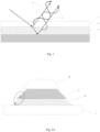
Fig. 1 is a schematic view showing the forming an anti-reflection layer on a metal layer; -
Figs. 2A and2B are schematic views showing the cross sections of the metal pattern and the anti-reflection pattern; -
Figs. 3A and3B are schematic views showing the cross sections of the metal pattern and the anti-reflection pattern according to an embodiments of the present disclosure; -
Fig. 4 is a schematic view showing the forming the metal layer and the anti-reflection layer according to an embodiment of the present disclosure; -
Fig. 5 is a schematic view showing the forming a photoresist pattern according to an embodiment of the present disclosure. - 1 base substrate; 2 anti-reflection layer; 3 metal layer; 4 first light; 5 second light; 6 anti-reflection pattern; 7 metal pattern; 8 photoresist pattern; 9 conductive pattern.
- In order to make the technical problems to be solved, the technical solutions, and the advantages of the examples of the present disclosure, the present disclosure will be described hereinafter in conjunction with the drawings and specific examples.
- As shown in
Fig. 1 , themetal layer 3, such as the gate metal layer, is located on the light emitting side of the display substrate, and ambient light is incident on themetal layer 3 and reflected by themetal layer 3 after being incident through thebase substrate 1, so that the substrate will still emit light in a black state. In order to reduce the reflection of the display substrate to the ambient light, the anti-reflection layer 2 can be added on the light emitting side of themetal layer 3, so that after the ambient light is incident on the surfaces of themetal layer 3, the second light 5 and thefirst light 4 reflected by the two surfaces will interfere with and offset each other, thereby achieving an anti-reflection effect. - An embodiment of the present disclosure provides a display substrate, as shown in
Figs. 2A and2B , including abase substrate 1, ametal pattern 7 on thebase substrate 1, and ananti-reflection pattern 6 on a surface of themetal pattern 7 proximate to thebase substrate 1, so that the reflection of the ambient light by the display substrate can be reduced through theanti-reflection pattern 6. - The anti-reflection layer 2 is made of molybdenum oxide MoOx, and the
metal layer 3 is made of copper. The etching rate of molybdenum oxide in the acidic etching solution is greater than that of copper in the acidic etching solution. In this way, in the process of manufacturing the display substrate, when themetal layer 3 and the anti-reflection layer 2 are etched by an acidic etching solution using aphotoresist 8 as a mask, as shown inFig. 2A , the undercut phenomenon as shown in the dotted frame will occur. Since the anti-reflection layer 2 has a greater etching rate in the acidic etching solution, the slope angle β of the longitudinal section of the formedanti-reflection pattern 6 is less than the slope angle α of the longitudinal section of the formedmetal pattern 7. The longitudinal section of themetal pattern 7 is the section of themetal pattern 7 in the first direction, the first direction is perpendicular to thebase substrate 1 and perpendicular to the extending direction of themetal pattern 7, the longitudinal section of theanti-reflection pattern 6 being a cross section of theanti-reflection pattern 6 in the second direction, the second direction being perpendicular to thebase substrate 1 and perpendicular to the extension direction of theanti-reflection pattern 6. The undercut phenomenon will affect the connection between themetal pattern 7 and other conductive patterns. For example, when other layers of the conductive patterns are connected to themetal pattern 7, as shown inFig. 2B , theconductive pattern 9 in contact with themetal pattern 7 will break at the undercut A. In this way, in the case that three is disconnection at the undercut, it will result in a defective product of the display substrate. - To avoid undercut phenomenon, an embodiment of the claimed invention provides a display substrate, as shown in
Figs. 3A and3B , including abase substrate 1, ametal pattern 7 on thebase substrate 1, and ananti-reflection pattern 6 located on a surface of themetal pattern 7 proximate to thebase substrate 1, in which a difference between the first slope angle β of theanti-reflection pattern 6 and the second slope angle α of themetal pattern 7 is less than a first threshold, and a distance d between a first edge of a side surface of the anti-reflection pattern proximate to the metal pattern and a second edge of a side surface of the metal pattern proximate to the anti-reflection pattern is less than a second threshold, and in which the first slope angle β is an acute angle formed between the side surface of theanti-reflection pattern 6 and thebase substrate 1, the second slope angle α is the acute angle formed between a side surface of themetal pattern 7 and thebase substrate 1, and the first edge and the second edge are located on a same side of theanti-reflection pattern 6. - The
anti-reflection pattern 6 is proximate to themetal pattern 7 and is located between themetal pattern 7 and thebase substrate 1. When themetal pattern 7 is located on the light exiting side of thebase substrate 1, as shown inFigs. 3A and3B , theanti-reflection pattern 6 may be adjacent to thebase substrate 1, that is, in contact with thebase substrate 1. - In this embodiment, a difference between the first slope angle β of the
anti-reflection pattern 6 and the second slope angle α of themetal pattern 7 is less than the first threshold, and a distance between the first edge and the second edge is less than the second threshold, thereby avoiding the undercut phenomenon, optimizing the connection between themetal pattern 7 and other conductive patterns, and improving the product yield of the display substrate. - Specifically, the first threshold is 5°, the second threshold is 10 nm, the difference between the first slope angle β of the
anti-reflection pattern 6 and the second slope angle α of themetal pattern 7 is less than 5°, the distance d between the first edge and the second edge is less than the second threshold. As shown inFig. 3B , when otherconductive patterns 9 are connected to themetal pattern 7, it will not break at the side surface of themetal pattern 7 and theanti-reflection pattern 6, thereby optimizing the connection between themetal pattern 7 and otherconductive patterns 9 and improving the product yield of the display substrate. - In a specific embodiment, the first slope angle β is equal to the second slope angle α, and the first edge coincides with the second edge, that is, d = 0, thereby eliminating the undercut phenomenon, so that the side surface of the
anti-reflection pattern 6 and the side surface of themetal pattern 7 can be located on a same plane. In this way, when other conductive patterns are connected to themetal pattern 7, there is no disconnection, thereby optimizing the connection between themetal pattern 7 and other conductive patterns, and improving the product yield of the display substrate. - Among them, the first slope angle may be in a range of 55° to 65°, and the second slope angle may be in a range of 55° to 65°.
- Among them, when the
metal pattern 7 is a signal line, the second slope angle of themetal pattern 7 is (A-5)° to (A+5)°, and a line width of the signal line is (D-1) µm to (D+1) µm, in which A is a preset reference value of the second slope angle, D is a preset reference value of the width of the signal line. A may be about 60°, and D may be in a range of 20 µm to 40 µm. The line width of themetal pattern 7 is a width of an orthogonal projection of themetal pattern 7 on the base substrate in a third direction, and the third direction is perpendicular to the extending direction of the metal pattern. The above embodiments can ensure the size uniformity of themetal pattern 7, and optimize the signal transmission performance of the display substrate. Among them, the signal line of the display substrate includes, but is not limited to, a gate line, a data line, and a common electrode line. - Specifically, the second slope angle and line width of the
metal pattern 7 at different positions may be equal, that is, the sizes of themetal pattern 7 at different positions are the same. - Among them, the thickness of the
anti-reflection pattern 6 is set such that the optical path difference of the reflected light on the upper and lower surfaces of theanti-reflection pattern 6 is an odd multiple of the half wavelength of the reflected light, and the thickness of theanti-reflection pattern 6 satisfies:
anti-reflection pattern 6, n may be in a range of 2.2 to 2.3, h is the thickness of the anti-reflection pattern, k is a positive integer, and λ is a wavelength of incident light. - In this way, after the ambient light is incident on the surfaces of the
metal pattern 7 and theanti-reflection pattern 6, the light reflected by the upper and lower surfaces of theanti-reflection pattern 6 will interfere with and offset each other, thereby achieving anti-reflection. Specifically, the thickness of theanti-reflection pattern 6 can be adjusted according to the wavelength of the incident light, as long as the optical path difference of the reflected light on the upper and lower surfaces of theanti-reflection pattern 6 is an odd multiple of the half wavelength of the reflected light. In addition, the wavelength is mostly around 550 nm, and most of the light is perpendicular to theanti-reflection pattern 6, so that λ in the above formula (1) can be 550 nm. When λ is equal to 550 nm and k = 1, the display substrate can reduce to the reflectance of light with a wavelength of 450 nm to 600 nm 10% or less, thereby greatly reducing the reflection of the display substrate on the ambient light. - Optionally, the thickness of the
anti-reflection pattern 6 may be in a range of 50 nm to 60 nm. - The metal pattern in this embodiment is a metal pattern arranged on the light emitting side of the display substrate. In some display substrates, the gate metal layer pattern is arranged on the light emitting side of the display substrate. In order to reduce the reflection of the ambient light by the gate metal layer pattern, an anti-reflection pattern is arranged between the gate metal layer pattern and the base substrate, the difference between the first slope angle of the anti-reflection pattern and the second slope angle of the gate metal layer pattern is less than the first threshold, and the distance between the first edge and the second edge of the metal pattern is less than the second threshold.
- Since copper has good conductivity, the
metal pattern 7 is made of copper. Theanti-reflection pattern 6 is made of molybdenum oxide. - Since the etching rate of molybdenum oxide in the acidic etching solution is greater than that of copper in the acidic etching solution, in order to avoid the undercut phenomenon, the composition of the
anti-reflection pattern 6 needs to be adjusted, and then the etching rate ofanti-reflection pattern 6 in acidic etching solution is adjusted. In this embodiment, and according to the claimed invention, a corrosion-resistant metal is doped in theanti-reflection pattern 6, in which the corrosion-resistant metal is a metal having strong resistance to oxidation of oxygen and other corrosion, and will react with usual acid. Specifically, the corrosion-resistant metal is selected from at least one of: ruthenium, rhodium, palladium, silver, osmium, iridium, platinum, and gold. The etching rate of theanti-reflection pattern 6 in the acidic etching solution can be reduced by doping theanti-reflection pattern 6 with corrosion-resistant metal, and the etching rate of theanti-reflection pattern 6 in the acidic etching solution can be adjusted by adjusting the content of the corrosion-resistant metal inanti-reflection pattern 6, so that the etching rate of theanti-reflection pattern 6 in the acidic etching solution is close to or the same as the etching rate of themetal pattern 7 in the acidic etching solution, thereby reducing or avoiding the undercut phenomenon. - After the corrosion-resistant metal is doped into the
anti-reflection pattern 6, the contact resistance between theanti-reflection pattern 6 and themetal pattern 7 can also be reduced. When themetal pattern 7 is a signal line, the signal transmission condition on the signal line can be optimized. - When the
metal pattern 7 is a gate metal pattern, in this embodiment and according to the claimed invention, since the distance between the first edge and the second edge is reduced, after the gate insulating layer is formed on the gate metal pattern, the parasitic capacitance between themetal pattern 7 and the data line of the display substrate can also be reduced, thereby preventing the electrical signal on themetal pattern 7 from affecting the data voltage on the data line, and further avoiding flickering of the picture and improving the display effect of the display device. - Specifically, in the
anti-reflection pattern 6, the molar ratio of the corrosion-resistant metal to molybdenum is (4: 100) to (6: 100), so that the etching rate of theanti-reflection pattern 6 in the acidic etching solution is close to the etching rate of themetal pattern 7 in the acidic etching solution. - In this embodiment, the etching rate of the anti-reflection pattern in the acidic etching solution is adjusted by doping the anti-reflection pattern with a corrosion-resistant metal, so that the etching rate of the anti-reflection pattern in the acidic etching solution is close to the etching rate of the metal pattern in the acidic etching solution. In this way, after the anti-reflection pattern and the metal pattern is formed by etching, so that the undercut at the junction of the anti-reflection pattern and the metal pattern can be avoided, thereby improving the connection between other conductive patterns and the metal pattern, and improving the product yield of the display substrate.
- An embodiment of the present disclosure further provides a display device, including the display substrate as described above and a color filter substrate oppositely arranged to form a cell with the display substrate, in which the display substrate is located on a light exiting side of the color filter substrate. The display device may be a liquid crystal display device or an organic light emitting diode display device. The display device may be any product or component having a display function, such as a television, a display, a digital photo frame, a mobile phone, a tablet computer, etc., in which the display device further includes a flexible circuit board, a printed circuit board, and a backplane.
- An embodiment of the present disclosure further provides a method for preparing a display substrate, including: as shown in
Fig. 4 , providing abase substrate 1; forming an anti-reflection layer 2 and ametal layer 3 in sequence on thebase substrate 1; coating photoresist on themetal layer 3, as shown inFig. 5 , and exposing and developing of the photoresist to form aphotoresist pattern 8; as shown inFig. 3A , forming ananti-reflection layer pattern 6 and ametal pattern 7 respectively by simultaneously etching the anti-reflection layer 2 and themetal layer 3 with an etching solution using thephotoresist pattern 8 as a mask, since the difference between the etch rate of the anti-reflection layer 2 and the etch rate of themetal layer 3 under the same etching condition is less than the rate threshold, a difference between a first slope angle β of the formedanti-reflection pattern 6 and a second slope angle α of the formedmetal pattern 7 is less than a first threshold, and a distance d between a first edge of a side surface of theanti-reflection pattern 6 proximate to themetal pattern 7 and a second edge of a side surface of themetal pattern 6 proximate to theanti-reflection pattern 7 is less than a second threshold, the first slope angle is an acute angle formed between a side surface of theanti-reflection pattern 6 and thebase substrate 1, the second slope angle is an acute angle formed between a side surface of themetal pattern 7 and thebase substrate 1, and the first edge and the second edge are located on a same side of theanti-reflection pattern 6. - The rate threshold can be specifically 0.5 nm/s. Of course, the value of the rate threshold is not limited to 0.5 nm/s, and can also be other values, but the value of the rate threshold needs to ensure that the difference between the first slope angle β of the resulting
anti-reflection pattern 6 and the second slope angle α of themetal pattern 7 is less than the first threshold and d is less than the second threshold. - In this embodiment, a difference between the first slope angle β of the
anti-reflection pattern 6 and the second slope angle α of themetal pattern 7 is less than the first threshold, and d is less than the second threshold, thereby avoiding the undercut phenomenon, optimizing the connection between themetal pattern 7 and other conductive patterns, and improving the product yield of the display substrate. In order to ensure that the difference between the first slope angle β of theanti-reflection pattern 6 and the second slope angle α of themetal pattern 7 is less than the first threshold and d is less than the second threshold, the composition of the anti-reflection layer 2 needs to be adjusted, and the etching rate of the anti-reflection layer 2 in the etching solution is further adjusted, so that the etching rate of the anti-reflection layer 2 in the etching solution is close to or the same as the etching rate of themetal layer 3 in the etching solution. - Specifically, the first threshold is 5°, the second threshold is 10 nm, the difference between the first slope angle β of the
anti-reflection pattern 6 and the second slope angle α of themetal pattern 7 is less than 5°, the distance d between the first edge and the second edge is less than the second threshold. When other conductive patterns are connected to the metal pattern, it may optimize the connection between themetal pattern 7 and other conductive patterns and improve the product yield of the display substrate. - The etching rate of the anti-reflection layer 2 may be equal to the etching rate of the
metal layer 3 under the same etching condition, so that the first slope angle β is equal to the second slope angle α, and the first edge coincides with the second edge, that is, d = 0, thereby eliminating the undercut phenomenon, and so that the side surface of theanti-reflection pattern 6 and the side surface of themetal pattern 7 can be located on a same plane. In this way, when other conductive patterns are connected to themetal pattern 7, there is no disconnection, thereby optimizing the connection between themetal pattern 7 and other conductive patterns, and improving the product yield of the display substrate. - The thickness of the
anti-reflection pattern 6, that is, the thickness of the anti-reflection layer 2 is set such that the optical path difference of the reflected light on the upper and lower surfaces of theanti-reflection pattern 6 is an odd multiple of the half wavelength of the reflected light and the thickness of 6 satisfies:
anti-reflection pattern 6, n may be 2.2 to 2.3, h is the thickness of the anti-reflection pattern, k is a positive integer, and λ is a wavelength of incident light. - In this way, after the ambient light is incident on the surfaces of the
metal pattern 7 and theanti-reflection pattern 6, the light reflected by the upper and lower surfaces of theanti-reflection pattern 6 will interfere with and offset each other, thereby achieving anti-reflection. Specifically, the thickness of theanti-reflection pattern 6 can be adjusted according to the wavelength of the incident light, as long as the optical path difference of the reflected light on the upper and lower surfaces of theanti-reflection pattern 6 is an odd multiple of the half wavelength of the reflected light. In addition, the wavelength is mostly around 550 nm, and most of the light is perpendicular to theanti-reflection pattern 6, so that λ in the above formula (1) can be 550 nm. When λ is equal to 550 nm and k = 1, the display substrate can reduce to the reflectance of light with a wavelength of 450 nm to 600 nm 10% or less, thereby greatly reducing the reflection of the display substrate on the ambient light. - Since copper has good conductivity, the
metal layer 3 is copper. The anti-reflection layer 2 is made of molybdenum oxide. - Since the etching rate of molybdenum oxide in the acidic etching solution is greater than that of copper in the acidic etching solution, in order to avoid the undercut phenomenon, the composition of the anti-reflection layer 2 needs to be adjusted, and then the etching rate of anti-reflection layer 2 in acidic etching solution is adjusted. In this embodiment and according to the claimed invention, a corrosion-resistant metal is doped in the anti-reflection layer 2, in which the corrosion-resistant metal is a metal having strong resistance to oxidation of oxygen and other corrosion, and will react with usual acid. Specifically, the corrosion-resistant metal is selected from at least one of: ruthenium, rhodium, palladium, silver, osmium, iridium, platinum, and gold. The etching rate of the anti-reflection layer 2 in the acidic etching solution can be reduced by doping the anti-reflection layer 2 with corrosion-resistant metal, and the etching rate of the anti-reflection layer 2 in the acidic etching solution can be adjusted by adjusting the content of the corrosion-resistant metal in anti-reflection layer 2, so that the etching rate of the anti-reflection pattern 2 in the acidic etching solution is close to or the same as the etching rate of the
metal layer 3 in the acidic etching solution, thereby avoiding the undercut phenomenon. - In a specific embodiment, when the
metal layer 3 is made of copper and the anti-reflection layer 2 is made of molybdenum oxide doped with a corrosion-resistant metal, a configuration according to the claimed invention, the forming the anti-reflection layer and the metal layer in sequence on the base substrate includes: bombarding a target made of molybdenum oxide doped with a corrosion-resistant metal by using a first plasma, to form the anti-reflection layer on the base substrate; and bombarding a target made of copper by using a second plasma, to form the metal layer on the base substrate. - The first plasma and the second plasma may be the same or different.
- Specifically, molybdenum oxide powder and corrosion-resistant metal powder can be sintered to prepare the target made of molybdenum oxide doped with corrosion-resistant metal.
- Specifically, in a molybdenum oxide target material doped with a corrosion-resistant metal, the molar ratio of the corrosion-resistant metal to molybdenum is (4:100) to (6:100), so that the etching rate of the anti-reflection layer 2 in the acidic etching solution is close to the etching rate of the
metal layer 3 in the acidic etching solution. - In a specific embodiment, during the formation of the anti-reflection layer 2, the gas flow rate of the sputtering gas for forming the first plasma may be in a range of 600 sccm to 800 sccm (standard milliliters per minute), the gas pressure for depositing may be in a range of 0.25 Pa to 0.35 Pa, and the sputtering power can be in a range of 7.5 kw to 8.5 kw. The film-forming rate of the anti-reflection layer 2 may be in a range of 1.3 nm/s to 1.4 nm/s.
- In addition to adjusting the composition of the anti-reflection layer 2, the etching rate of the anti-reflection layer 2 in the etching solution can also be adjusted by adjusting the composition of the etching solution. In a specific embodiment, the etching solution may be a mixed solution of H2SO4 and H2O2, in which the volume ratio of H2O2 in the mixed solution may be in a range of 3% to 5%, and the ratio is beneficial to the etching rate of the anti-reflection layer 2 in the acidic etching solution close to the etching rate of
metal layer 3 in the acidic etching solution. - According to the claimed invention, before the
metal layer 3 and the anti-reflection layer 2 are etched by the etching solution, the metal ion concentration in the etching solution can also be increased, thereby reducing the etching rate of themetal layer 3 and the anti-reflection layer 2 in the etching solution. If the etching rate is too fast, it is difficult to avoid uneven etching. After reducing the etching rate of themetal layer 3 and the anti-reflection layer 2 in the etching solution, it can improve the uniformity of the size of the formedmetal pattern 7 and the anti-reflection pattern 2, which is conducive to improving the product yield of display substrates and enhancing the market competitiveness of products. Therefore, the etching solution for etching the metal layer and the anti-reflection layer includes metal ions, in which the metal ion and the metal layer share the same metal element. - When the
metal pattern 7 is a signal line, the second slope angle of themetal pattern 7 is (A-5)° to (A+5)°, and a line width of the signal line is (D-1) µm to (D+1) µm, in which A is a preset reference value of the second slope angle, D is a preset reference value of the width of the signal line, a line width of themetal pattern 7 is a width of an orthogonal projection of themetal pattern 7 on the base substrate in a third direction, and the third direction is perpendicular to the extending direction of the metal pattern. In this way, it can ensure the size uniformity of themetal pattern 7, and optimize the signal transmission performance of the display substrate. The signal line of the display substrate includes, but is not limited to, a gate line, a data line, and a common electrode line. - Specifically, the second slope angle and line width of the
metal pattern 7 at different positions may be equal, that is, the sizes of themetal pattern 7 at different positions are the same. - Specifically, when the
metal layer 3 is made of copper, the concentration of copper ions in the etching solution may be in a range of 200 ppm to 1500 ppm, thereby effectively reducing the etching rate of themetal layer 3 and the anti-reflection layer 2 in the etching solution, so as to ensure the uniformity of the size of themetal pattern 7 and the anti-reflection pattern 2. - When other metal materials are used for the
metal layer 3, which is not according to the claimed invention, the concentration of metal ions in the etching solution can also be adjusted to reduce the etching rate of themetal layer 3 and the anti-reflection layer 2 in the etching solution. For example, when the metal layer is made of aluminum, the concentration of aluminum ions in the etching solution can be increased, and so on. - After the corrosion-resistant metal is doped into the
anti-reflection pattern 6, the contact resistance between theanti-reflection pattern 6 and themetal pattern 7 can also be reduced. When themetal pattern 7 is a signal line, the signal transmission condition on the signal line can be optimized. - When the
metal pattern 7 is a gate metal pattern, in this embodiment, since the distance between the first edge and the second edge is reduced, after the gate insulating layer is formed on the gate metal pattern, the parasitic capacitance between themetal pattern 7 and the data line of the display substrate can also be reduced, thereby preventing the electrical signal on themetal pattern 7 from affecting the data voltage on the data line, and further avoiding flickering of the picture and improving the display effect of the display device. - In a specific example not according to the claimed invention, the method for preparing the display substrate includes the following steps.
- Step 1: as shown in
Fig. 4 , forming an anti-reflection layer 2 on thebase substrate 1. - A physical vapor deposition (PVD) device can be used to deposit a layer of molybdenum oxide film doped with tantalum as the anti-reflection layer. Specifically, in a vacuum environment, under the combined action of voltage and magnetic field, the molybdenum oxide target is bombarded with ionized inert gas ions such as Ar particles, so that the molybdenum oxide target is ejected in the form of ions, atoms or molecules and deposited on the base substrate to form a molybdenum oxide film. In the molybdenum oxide target, the molar ratio of tantalum to molybdenum is (4:100) to (6:100), the flow rate of Ar gas is controlled to 700 sccm, the deposition pressure is adjusted to 0.3 Pa, the deposition power is 8 kw, the deposition rate is controlled to 1.35 nm/s, to ensure that the deposited film is uniform, and the anti-reflection layer 2 with a thickness of about 54 nm is formed.
- Step 2: as shown in
Fig. 4 , depositing ametal layer 3 on the anti-reflection layer 2. - Specifically, a layer of copper can be deposited as a
metal layer 3 using PVD equipment. - Step 3: coating photoresist on the
metal layer 3, and exposing and developing the photoresist using a mask plate, as shown inFig. 5 , to form aphotoresist pattern 8; - Step 4: etching the
metal layer 3 and the anti-reflection layer 2 by a mixed solution of H2SO4 and H2O2 with thephotoresist pattern 8 as a mask, as shown inFig. 3A , to obtain ametal pattern 7 and ananti-reflection pattern 6. - In the mixed solution of H2SO4 and H2O2, the volume ratio of H2O2 accounts for 4%, and the concentration of Cu ion is in a range of 200 ppm to 1500 ppm.
- Specifically, the copper block can be etched by a mixed solution of H2SO4 and H2O2 to increase the concentration of Cu ions in the mixed solution of H2SO4 and H2O2. After increasing the concentration of Cu ions in the mixed solution of H2SO4 and H2O2, the etch rate of the mixed solution of H2SO4 and H2O2 to the
metal layer 3 and the anti-reflection layer 2 can be reduced, thereby further improve the uniformity of the size of themetal pattern 7 and theanti-reflection pattern 6. - At the same time, the anti-reflection layer 2 uses tantalum-doped molybdenum oxide, and thus the etching rate of the anti-reflection layer 2 in the mixed solution is reduced. In this way, it will reduce the difference in the etching rate from copper, thereby avoiding the occurrence of the undercut phenomenon.
- Step 5: stripping a remaining photoresist.
- After the above steps, the production of the
metal pattern 7 and theanti-reflection pattern 6 can be completed. Themetal pattern 7 may be the gate metal layer pattern of the display substrate. When theanti-reflection pattern 6 is made of molybdenum oxide doped with tantalum, theanti-reflection pattern 6 also has a certain conductivity, and is parallel to the gate metal layer pattern to improve the conductive property of the gate metal layer pattern, and further improve the product yield of the display substrate. - Of course, the
metal pattern 7 is not limited to the gate metal layer pattern of the display substrate, but may also be the source-drain metal layer pattern of the display substrate. When themetal pattern 7 is the source-drain metal layer pattern of the display substrate, the provision of theanti-reflection pattern 6 on a surface of themetal pattern 7 facing thebase substrate 1 also helps to reduce the reflectivity of the display substrate, and theanti-reflection pattern 6 connected in parallel with themetal pattern 7 is capable of improving the conductivity of the source-drain metal layer pattern and further improve the product yield of the display substrate rate. - After the production of the
metal pattern 7 and theanti-reflection pattern 6 is completed by the above steps, the other film layer of the display substrate, such as the gate insulating layer, the active layer, the anode, the cathode, etc., can be continued to be prepared, so as to complete the production of the display substrate. - In the method embodiments of the present disclosure, the serial numbers of the steps cannot be used to define the sequence of the steps. As for one skilled in the art, the changes in the order of steps without paying creative work also fall within the scope of the present disclosure.
- Unless otherwise defined, technical terms or scientific terms used herein have the normal meaning commonly understood by one skilled in the art in the field of the present disclosure. The words "first", "second", and the like used herein does not denote any order, quantity, or importance, but rather merely serves to distinguish different components. The "including", "comprising", and the like used in the present disclosure means that the element or item appeared in front of the word encompasses the element or item and their equivalents listed after the word, and does exclude other elements or items. The word "connected" or "connecting" and the like are not limited to physical or mechanical connections, but may include electrical connections, whether direct or indirect. "On", "under", "left", "right" and the like are only used to represent relative positional relationships, and when the absolute position of the described object is changed, the relative positional relationship may also be changed, accordingly.
- It will be understood that when an element, such as a layer, film, region, or substrate, is referred to as being "on" or "under" another element, the element may be directly "on" or "under" another element, or there may be an intermediate element.
- The above descriptions are preferred embodiments of the present disclosure. It should be noted that one skilled in the art would make several improvements and substitutions without departing from the principles of the present disclosure.
Claims (14)
- A display substrate, comprising:a base substrate (1);a metal pattern (7) located on the base substrate (1); andan anti-reflection pattern (6) located on a surface of the metal pattern (7) proximate to the base substrate (1),wherein a difference between a first slope angle of the anti-reflection pattern (6) and a second slope angle of the metal pattern (7) is less than a first threshold, and a distance between a first edge of a side surface of the anti-reflection pattern (6) proximate to the metal pattern (7) and a second edge of a side surface of the metal pattern (7) proximate to the anti-reflection pattern (6) is less than a second threshold;the first slope angle is an acute angle formed between the side surface of the anti-reflection pattern (6) and the base substrate (1), the second slope angle is an acute angle formed between the side surface of the metal pattern (7) and the base substrate (1), and the first edge and the second edge are located on a same side of the anti-reflection pattern (6),wherein the metal pattern (7) is a gate metal layer pattern of the display substrate, a material of the metal pattern (7) is copper, and a material of the anti-reflection pattern (6) is molybdenum oxide doped with a corrosion-resistant metalwherein in the anti-reflection pattern (6), a molar ratio of the corrosion-resistant metal to molybdenum is 4:100 to 6:100 and characterized in that the: corrosion-resistant metal is at least one selected from: ruthenium, rhodium, palladium, silver, osmium, iridium, platinum and gold.
- The display substrate of claim 1, wherein the first threshold is 5°, and the second threshold is 10 nm.
- The display substrate of claim 2, wherein the first slope angle is equal to the second slope angle, and the first edge coincides with the second edge.
- The display substrate of claim 1, wherein the first slope angle is in a range of 55° to 65°, and the second slope angle is in a range of 55° to 65°.
- The display substrate of claim 1, wherein the metal pattern (7) comprises a signal line, a second slope angle of the signal line is (A-5)° to (A+5)°, and a line width of the signal line is (D-1) µm to (D+1) µm, wherein A is a reference value of the second slope angle and D is a reference value of the width of the signal line.
- The display substrate of claim 1, wherein a thickness of the anti-reflection pattern (6) satisfies:

- A display device, comprising the display substrate according to any one of claims 1 to 6 and a color filter substrate arranged oppositely to form a cell with the display substrate, wherein the display substrate is located on a light exiting side of the color filter substrate.
- A method for preparing a display substrate, comprising:providing a base substrate (1);forming an anti-reflection layer (2) and a metal layer (3) in sequence on the base substrate (1);coating a photoresist on the metal layer (3), and exposing and developing the photoresist to form a photoresist pattern (8);forming an anti-reflection pattern (6) and a metal pattern (7) respectively by simultaneously etching the anti-reflection layer (2) and the metal layer (3) with an etching solution using the photoresist pattern (8) as a mask, wherein a difference between a first slope angle of the anti-reflection pattern (6) and a second slope angle of the metal pattern (7) is less than a first threshold, and a distance between a first edge of a side surface of the anti-reflection pattern (6) proximate to the metal pattern (7) and a second edge of a side surface of the metal pattern (7) proximate to the anti-reflection pattern (6) is less than a second threshold, and wherein the first slope angle is an acute angle formed between a side surface of the anti-reflection pattern (6) and the base substrate (1), the second slope angle is an acute angle formed between a side surface of the metal pattern (7) and the base substrate (1), and the first edge and the second edge are located on a same side of the anti-reflection pattern (6),wherein the metal pattern (7) is a gate metal layer pattern of the display substrate, a material of the metal pattern (7) is copper, and a material of the anti-reflection pattern (6) is molybdenum oxide doped with a corrosion-resistant metal andcharacterized in that the anti-reflection pattern (6) is doped with a corrosion-resistant metal, the corrosion-resistant metal is at least one selected from: ruthenium, rhodium, palladium, silver, osmium, iridium, platinum, and gold,wherein before the metal layer (3) and the anti-reflection layer (2) are etched by the etching solution, the etching solution includes a metal ion, and the metal ion and the metal layer (3) are made of a same metal element.
- The method of claim 8, wherein a difference between an etching rate of the anti-reflection layer (2) and an etching rate of the metal layer (3) in a same etching conditions is less than a rate threshold, optionally the rate threshold is 0.5 nm/s.
- The method of claim 8, wherein the forming the anti-reflection layer (2) and the metal layer (3) in sequence on the base substrate (1) comprises:bombarding a target made of molybdenum oxide doped with a corrosion-resistant metal by using a first plasma, to form the anti-reflection layer (2) on the base substrate (1); andbombarding a target made of copper by using a second plasma, to form the metal layer (3) on the base substrate (1).
- The method of claim 10, wherein in the target made of molybdenum oxide doped with the corrosion-resistant metal, a molar ratio of the corrosion-resistant metal to molybdenum is (4:100) to (6:100).
- The method of claim 10, wherein a film-forming rate of the anti-reflection layer (2) is in a range of 1.3 nm/s to 1.4 nm/s.
- The method of any one of claims 8 to 12, wherein the etching solution is a mixed solution of H2SO4 and H2O2, and a volume ratio of H2O2 in the mixed solution is in a range of 3% to 5%.
- The method of any one of claims 8 to 12, wherein a concentration of copper ions in the etching solution is in a range of 200 ppm to 1500 ppm.
Applications Claiming Priority (1)
| Application Number | Priority Date | Filing Date | Title |
|---|---|---|---|
| PCT/CN2019/101571 WO2021031118A1 (en) | 2019-08-20 | 2019-08-20 | Display substrate and manufacturing method therefor, and display device |
Publications (3)
| Publication Number | Publication Date |
|---|---|
| EP3992701A1 EP3992701A1 (en) | 2022-05-04 |
| EP3992701A4 EP3992701A4 (en) | 2022-05-18 |
| EP3992701B1 true EP3992701B1 (en) | 2024-11-06 |
Family
ID=74646387
Family Applications (1)
| Application Number | Title | Priority Date | Filing Date |
|---|---|---|---|
| EP19930165.6A Active EP3992701B1 (en) | 2019-08-20 | 2019-08-20 | Display substrate and manufacturing method therefor, and display device |
Country Status (4)
| Country | Link |
|---|---|
| US (1) | US11251206B2 (en) |
| EP (1) | EP3992701B1 (en) |
| CN (1) | CN113168039A (en) |
| WO (1) | WO2021031118A1 (en) |
Family Cites Families (11)
| Publication number | Priority date | Publication date | Assignee | Title |
|---|---|---|---|---|
| TWI489519B (en) | 2004-04-28 | 2015-06-21 | 半導體能源研究所股份有限公司 | Wiring on substrate, semiconductor device and method of manufacturing same |
| US10873045B2 (en) * | 2005-11-29 | 2020-12-22 | Banpil Photonics, Inc. | High efficiency photovoltaic cells and manufacturing thereof |
| WO2007139210A1 (en) * | 2006-05-31 | 2007-12-06 | Semiconductor Energy Laboratory Co., Ltd. | Display device |
| CN103231570B (en) | 2013-04-11 | 2016-03-30 | 合肥京东方光电科技有限公司 | A kind of thin layer and preparation method thereof, substrate for display, liquid crystal display |
| US11926558B2 (en) * | 2015-03-27 | 2024-03-12 | Lg Chem Ltd. | Conductive structure, manufacturing method therefor, and electrode comprising conductive structure |
| KR102030227B1 (en) * | 2015-05-08 | 2019-10-08 | 주식회사 엘지화학 | Thin film transistor substrate and display device comprising thereof |
| KR102127545B1 (en) * | 2015-12-07 | 2020-06-29 | 주식회사 엘지화학 | Conductive structure body, method for manufacturing thereof and electrode comprising conductive structure body |
| CN107393933B (en) * | 2017-07-31 | 2020-08-04 | 京东方科技集团股份有限公司 | Manufacturing method of array substrate, array substrate and display panel |
| KR102446344B1 (en) * | 2017-11-16 | 2022-09-22 | 삼성디스플레이 주식회사 | Method of manufacturing display device and wiring |
| CN107946322A (en) * | 2017-12-15 | 2018-04-20 | 京东方科技集团股份有限公司 | Array substrate, manufacturing method thereof, and display device |
| CN108121098B (en) * | 2017-12-19 | 2019-08-06 | 友达光电股份有限公司 | Metal structure, manufacturing method and display panel for application thereof |
-
2019
- 2019-08-20 EP EP19930165.6A patent/EP3992701B1/en active Active
- 2019-08-20 CN CN201980001407.7A patent/CN113168039A/en active Pending
- 2019-08-20 US US16/771,201 patent/US11251206B2/en active Active
- 2019-08-20 WO PCT/CN2019/101571 patent/WO2021031118A1/en not_active Ceased
Also Published As
| Publication number | Publication date |
|---|---|
| EP3992701A1 (en) | 2022-05-04 |
| EP3992701A4 (en) | 2022-05-18 |
| WO2021031118A1 (en) | 2021-02-25 |
| CN113168039A (en) | 2021-07-23 |
| US11251206B2 (en) | 2022-02-15 |
| US20210057448A1 (en) | 2021-02-25 |
Similar Documents
| Publication | Publication Date | Title |
|---|---|---|
| US10886410B2 (en) | Thin film transistor, display substrate, method for manufacturing the same, and display device | |
| KR101522481B1 (en) | Method for fabricating array substrate, array substrate and display device | |
| KR101711260B1 (en) | Conductive film, method for manufacturing the same and display device comprising the same | |
| CN105144045B (en) | Conductive structure and its manufacture method | |
| US10651204B2 (en) | Array substrate, its manufacturing method and display device | |
| US11293088B2 (en) | Conductive structure, method for manufacturing same, and electrode comprising conductive structure | |
| KR19990067926A (en) | Electrode plate having transparent type or reflective type multi-layered conductive film and method for manufacturing the same | |
| US20010030170A1 (en) | Transparent conductive film and process for forming a transparent electrode | |
| US10539724B2 (en) | Array substrate, method for manufacture thereof and display device | |
| CN111524907A (en) | Display panel, preparation method thereof and display device | |
| CN110850656A (en) | Array substrate, manufacturing method thereof, display panel and display device | |
| KR101849449B1 (en) | Conductive structure body and method for manufacturing the same | |
| KR20040016908A (en) | Tft substrate, liquid crystal display using the same, and its manufacturing method | |
| US20190196285A1 (en) | Manufacturing method of array substrate and its upper electrode line pattern and liquid crystal display panel | |
| CN108565246A (en) | Thin film transistor base plate and preparation method thereof, dot structure, display device | |
| US11251206B2 (en) | Display substrate and method for preparing the same, and display device | |
| US9196734B2 (en) | Thin-film transistor substrate and method for fabricating the same, display | |
| US11966009B2 (en) | Display substrate and method for preparing the same, and display device | |
| US11333944B2 (en) | Array substrate and method of manufacturing the same, and display device | |
| CN112909040B (en) | Display module, manufacturing method thereof, display screen assembly and electronic equipment | |
| CN116057502A (en) | Transparent electrode laminate and touch sensor including the same | |
| US20250233299A1 (en) | Transparent antenna and method for fabricating the same, electronic device and method for driving the same | |
| CN219738130U (en) | Touch screen button bitmap layer stacking structure | |
| TWI831409B (en) | Touch panel and manufacturing method thereof | |
| CN114784022B (en) | Array substrate, manufacturing method thereof and display device |
Legal Events
| Date | Code | Title | Description |
|---|---|---|---|
| STAA | Information on the status of an ep patent application or granted ep patent |
Free format text: STATUS: UNKNOWN |
|
| STAA | Information on the status of an ep patent application or granted ep patent |
Free format text: STATUS: THE INTERNATIONAL PUBLICATION HAS BEEN MADE |
|
| PUAI | Public reference made under article 153(3) epc to a published international application that has entered the european phase |
Free format text: ORIGINAL CODE: 0009012 |
|
| STAA | Information on the status of an ep patent application or granted ep patent |
Free format text: STATUS: REQUEST FOR EXAMINATION WAS MADE |
|
| REG | Reference to a national code |
Ref legal event code: R079 Free format text: PREVIOUS MAIN CLASS: G02F0001133300 Ref country code: DE Ref legal event code: R079 Ref document number: 602019061770 Country of ref document: DE Free format text: PREVIOUS MAIN CLASS: G02F0001133300 Ipc: G02F0001136200 |
|
| 17P | Request for examination filed |
Effective date: 20201202 |
|
| AK | Designated contracting states |
Kind code of ref document: A1 Designated state(s): AL AT BE BG CH CY CZ DE DK EE ES FI FR GB GR HR HU IE IS IT LI LT LU LV MC MK MT NL NO PL PT RO RS SE SI SK SM TR |
|
| A4 | Supplementary search report drawn up and despatched |
Effective date: 20220420 |
|
| RIC1 | Information provided on ipc code assigned before grant |
Ipc: H01L 27/12 20060101ALI20220412BHEP Ipc: H01L 21/3213 20060101ALI20220412BHEP Ipc: G02F 1/1362 20060101AFI20220412BHEP |
|
| DAV | Request for validation of the european patent (deleted) | ||
| DAX | Request for extension of the european patent (deleted) | ||
| STAA | Information on the status of an ep patent application or granted ep patent |
Free format text: STATUS: EXAMINATION IS IN PROGRESS |
|
| 17Q | First examination report despatched |
Effective date: 20230804 |
|
| GRAP | Despatch of communication of intention to grant a patent |
Free format text: ORIGINAL CODE: EPIDOSNIGR1 |
|
| STAA | Information on the status of an ep patent application or granted ep patent |
Free format text: STATUS: GRANT OF PATENT IS INTENDED |
|
| INTG | Intention to grant announced |
Effective date: 20240703 |
|
| GRAS | Grant fee paid |
Free format text: ORIGINAL CODE: EPIDOSNIGR3 |
|
| GRAA | (expected) grant |
Free format text: ORIGINAL CODE: 0009210 |
|
| STAA | Information on the status of an ep patent application or granted ep patent |
Free format text: STATUS: THE PATENT HAS BEEN GRANTED |
|
| AK | Designated contracting states |
Kind code of ref document: B1 Designated state(s): AL AT BE BG CH CY CZ DE DK EE ES FI FR GB GR HR HU IE IS IT LI LT LU LV MC MK MT NL NO PL PT RO RS SE SI SK SM TR |
|
| REG | Reference to a national code |
Ref country code: GB Ref legal event code: FG4D |
|
| REG | Reference to a national code |
Ref country code: CH Ref legal event code: EP |
|
| REG | Reference to a national code |
Ref country code: DE Ref legal event code: R096 Ref document number: 602019061770 Country of ref document: DE |
|
| REG | Reference to a national code |
Ref country code: IE Ref legal event code: FG4D |
|
| REG | Reference to a national code |
Ref country code: LT Ref legal event code: MG9D |
|
| REG | Reference to a national code |
Ref country code: NL Ref legal event code: MP Effective date: 20241106 |
|
| PG25 | Lapsed in a contracting state [announced via postgrant information from national office to epo] |
Ref country code: HR Free format text: LAPSE BECAUSE OF FAILURE TO SUBMIT A TRANSLATION OF THE DESCRIPTION OR TO PAY THE FEE WITHIN THE PRESCRIBED TIME-LIMIT Effective date: 20241106 Ref country code: IS Free format text: LAPSE BECAUSE OF FAILURE TO SUBMIT A TRANSLATION OF THE DESCRIPTION OR TO PAY THE FEE WITHIN THE PRESCRIBED TIME-LIMIT Effective date: 20250306 Ref country code: PT Free format text: LAPSE BECAUSE OF FAILURE TO SUBMIT A TRANSLATION OF THE DESCRIPTION OR TO PAY THE FEE WITHIN THE PRESCRIBED TIME-LIMIT Effective date: 20250306 |
|
| PG25 | Lapsed in a contracting state [announced via postgrant information from national office to epo] |
Ref country code: FI Free format text: LAPSE BECAUSE OF FAILURE TO SUBMIT A TRANSLATION OF THE DESCRIPTION OR TO PAY THE FEE WITHIN THE PRESCRIBED TIME-LIMIT Effective date: 20241106 Ref country code: NL Free format text: LAPSE BECAUSE OF FAILURE TO SUBMIT A TRANSLATION OF THE DESCRIPTION OR TO PAY THE FEE WITHIN THE PRESCRIBED TIME-LIMIT Effective date: 20241106 |
|
| REG | Reference to a national code |
Ref country code: AT Ref legal event code: MK05 Ref document number: 1740015 Country of ref document: AT Kind code of ref document: T Effective date: 20241106 |
|
| PG25 | Lapsed in a contracting state [announced via postgrant information from national office to epo] |
Ref country code: BG Free format text: LAPSE BECAUSE OF FAILURE TO SUBMIT A TRANSLATION OF THE DESCRIPTION OR TO PAY THE FEE WITHIN THE PRESCRIBED TIME-LIMIT Effective date: 20241106 |
|
| PG25 | Lapsed in a contracting state [announced via postgrant information from national office to epo] |
Ref country code: ES Free format text: LAPSE BECAUSE OF FAILURE TO SUBMIT A TRANSLATION OF THE DESCRIPTION OR TO PAY THE FEE WITHIN THE PRESCRIBED TIME-LIMIT Effective date: 20241106 |
|
| PG25 | Lapsed in a contracting state [announced via postgrant information from national office to epo] |
Ref country code: NO Free format text: LAPSE BECAUSE OF FAILURE TO SUBMIT A TRANSLATION OF THE DESCRIPTION OR TO PAY THE FEE WITHIN THE PRESCRIBED TIME-LIMIT Effective date: 20250206 |
|
| PG25 | Lapsed in a contracting state [announced via postgrant information from national office to epo] |
Ref country code: LV Free format text: LAPSE BECAUSE OF FAILURE TO SUBMIT A TRANSLATION OF THE DESCRIPTION OR TO PAY THE FEE WITHIN THE PRESCRIBED TIME-LIMIT Effective date: 20241106 Ref country code: GR Free format text: LAPSE BECAUSE OF FAILURE TO SUBMIT A TRANSLATION OF THE DESCRIPTION OR TO PAY THE FEE WITHIN THE PRESCRIBED TIME-LIMIT Effective date: 20250207 Ref country code: AT Free format text: LAPSE BECAUSE OF FAILURE TO SUBMIT A TRANSLATION OF THE DESCRIPTION OR TO PAY THE FEE WITHIN THE PRESCRIBED TIME-LIMIT Effective date: 20241106 |
|
| PG25 | Lapsed in a contracting state [announced via postgrant information from national office to epo] |
Ref country code: PL Free format text: LAPSE BECAUSE OF FAILURE TO SUBMIT A TRANSLATION OF THE DESCRIPTION OR TO PAY THE FEE WITHIN THE PRESCRIBED TIME-LIMIT Effective date: 20241106 |
|
| PG25 | Lapsed in a contracting state [announced via postgrant information from national office to epo] |
Ref country code: RS Free format text: LAPSE BECAUSE OF FAILURE TO SUBMIT A TRANSLATION OF THE DESCRIPTION OR TO PAY THE FEE WITHIN THE PRESCRIBED TIME-LIMIT Effective date: 20250206 |
|
| PG25 | Lapsed in a contracting state [announced via postgrant information from national office to epo] |
Ref country code: SM Free format text: LAPSE BECAUSE OF FAILURE TO SUBMIT A TRANSLATION OF THE DESCRIPTION OR TO PAY THE FEE WITHIN THE PRESCRIBED TIME-LIMIT Effective date: 20241106 |
|
| PG25 | Lapsed in a contracting state [announced via postgrant information from national office to epo] |
Ref country code: DK Free format text: LAPSE BECAUSE OF FAILURE TO SUBMIT A TRANSLATION OF THE DESCRIPTION OR TO PAY THE FEE WITHIN THE PRESCRIBED TIME-LIMIT Effective date: 20241106 |
|
| PG25 | Lapsed in a contracting state [announced via postgrant information from national office to epo] |
Ref country code: EE Free format text: LAPSE BECAUSE OF FAILURE TO SUBMIT A TRANSLATION OF THE DESCRIPTION OR TO PAY THE FEE WITHIN THE PRESCRIBED TIME-LIMIT Effective date: 20241106 |
|
| PG25 | Lapsed in a contracting state [announced via postgrant information from national office to epo] |
Ref country code: RO Free format text: LAPSE BECAUSE OF FAILURE TO SUBMIT A TRANSLATION OF THE DESCRIPTION OR TO PAY THE FEE WITHIN THE PRESCRIBED TIME-LIMIT Effective date: 20241106 |
|
| PG25 | Lapsed in a contracting state [announced via postgrant information from national office to epo] |
Ref country code: SK Free format text: LAPSE BECAUSE OF FAILURE TO SUBMIT A TRANSLATION OF THE DESCRIPTION OR TO PAY THE FEE WITHIN THE PRESCRIBED TIME-LIMIT Effective date: 20241106 |
|
| PG25 | Lapsed in a contracting state [announced via postgrant information from national office to epo] |
Ref country code: CZ Free format text: LAPSE BECAUSE OF FAILURE TO SUBMIT A TRANSLATION OF THE DESCRIPTION OR TO PAY THE FEE WITHIN THE PRESCRIBED TIME-LIMIT Effective date: 20241106 |
|
| PG25 | Lapsed in a contracting state [announced via postgrant information from national office to epo] |
Ref country code: IT Free format text: LAPSE BECAUSE OF FAILURE TO SUBMIT A TRANSLATION OF THE DESCRIPTION OR TO PAY THE FEE WITHIN THE PRESCRIBED TIME-LIMIT Effective date: 20241106 |
|
| REG | Reference to a national code |
Ref country code: DE Ref legal event code: R097 Ref document number: 602019061770 Country of ref document: DE |
|
| PG25 | Lapsed in a contracting state [announced via postgrant information from national office to epo] |
Ref country code: SE Free format text: LAPSE BECAUSE OF FAILURE TO SUBMIT A TRANSLATION OF THE DESCRIPTION OR TO PAY THE FEE WITHIN THE PRESCRIBED TIME-LIMIT Effective date: 20241106 |
|
| PLBE | No opposition filed within time limit |
Free format text: ORIGINAL CODE: 0009261 |
|
| STAA | Information on the status of an ep patent application or granted ep patent |
Free format text: STATUS: NO OPPOSITION FILED WITHIN TIME LIMIT |
|
| PGFP | Annual fee paid to national office [announced via postgrant information from national office to epo] |
Ref country code: DE Payment date: 20250820 Year of fee payment: 7 |
|
| 26N | No opposition filed |
Effective date: 20250807 |
|
| REG | Reference to a national code |
Ref country code: CH Ref legal event code: H13 Free format text: ST27 STATUS EVENT CODE: U-0-0-H10-H13 (AS PROVIDED BY THE NATIONAL OFFICE) Effective date: 20260324 |
|
| PG25 | Lapsed in a contracting state [announced via postgrant information from national office to epo] |
Ref country code: MC Free format text: LAPSE BECAUSE OF FAILURE TO SUBMIT A TRANSLATION OF THE DESCRIPTION OR TO PAY THE FEE WITHIN THE PRESCRIBED TIME-LIMIT Effective date: 20241106 |
|
| PG25 | Lapsed in a contracting state [announced via postgrant information from national office to epo] |
Ref country code: LU Free format text: LAPSE BECAUSE OF NON-PAYMENT OF DUE FEES Effective date: 20250820 |
|
| PG25 | Lapsed in a contracting state [announced via postgrant information from national office to epo] |
Ref country code: CH Free format text: LAPSE BECAUSE OF NON-PAYMENT OF DUE FEES Effective date: 20250831 |
|
| GBPC | Gb: european patent ceased through non-payment of renewal fee |
Effective date: 20250820 |