EP3992672A1 - Optical element, optical system, and optical apparatus - Google Patents
Optical element, optical system, and optical apparatus Download PDFInfo
- Publication number
- EP3992672A1 EP3992672A1 EP21202894.8A EP21202894A EP3992672A1 EP 3992672 A1 EP3992672 A1 EP 3992672A1 EP 21202894 A EP21202894 A EP 21202894A EP 3992672 A1 EP3992672 A1 EP 3992672A1
- Authority
- EP
- European Patent Office
- Prior art keywords
- layer
- film
- optical element
- sio
- refractive index
- Prior art date
- Legal status (The legal status is an assumption and is not a legal conclusion. Google has not performed a legal analysis and makes no representation as to the accuracy of the status listed.)
- Granted
Links
Images





Classifications
-
- G—PHYSICS
- G02—OPTICS
- G02B—OPTICAL ELEMENTS, SYSTEMS OR APPARATUS
- G02B1/00—Optical elements characterised by the material of which they are made; Optical coatings for optical elements
- G02B1/10—Optical coatings produced by application to, or surface treatment of, optical elements
- G02B1/11—Anti-reflection coatings
- G02B1/113—Anti-reflection coatings using inorganic layer materials only
- G02B1/115—Multilayers
-
- H—ELECTRICITY
- H04—ELECTRIC COMMUNICATION TECHNIQUE
- H04N—PICTORIAL COMMUNICATION, e.g. TELEVISION
- H04N23/00—Cameras or camera modules comprising electronic image sensors; Control thereof
- H04N23/50—Constructional details
- H04N23/55—Optical parts specially adapted for electronic image sensors; Mounting thereof
-
- H—ELECTRICITY
- H10—SEMICONDUCTOR DEVICES; ELECTRIC SOLID-STATE DEVICES NOT OTHERWISE PROVIDED FOR
- H10F—INORGANIC SEMICONDUCTOR DEVICES SENSITIVE TO INFRARED RADIATION, LIGHT, ELECTROMAGNETIC RADIATION OF SHORTER WAVELENGTH OR CORPUSCULAR RADIATION
- H10F39/00—Integrated devices, or assemblies of multiple devices, comprising at least one element covered by group H10F30/00, e.g. radiation detectors comprising photodiode arrays
- H10F39/80—Constructional details of image sensors
- H10F39/805—Coatings
Definitions
- the present disclosure relates to an optical element.
- JP 2002-202401 discloses an antireflection film having an outermost layer, which is a layer (silicon oxide layer) including SiO 2 or SiO as a principal component, and a next layer, which is a layer (magnesium fluoride layer) including MgF 2 as a principal component.
- JP 2017-134404 discloses an antireflection film consisting of a multi-laminated layer in which silicon oxide layers and tantalum oxide layers are alternately laminated, a magnesium fluoride layer formed on the multi-laminated layer, and a silicon oxide layer as an outermost layer formed on the magnesium fluoride layer.
- the present disclosure provides an optical element, an optical system, and an optical apparatus each of which has high mechanical strength and high environmental durability.
- the present disclosure in a first aspect provides an optical element as specified in claims 1 to 11.
- the present disclosure in a second aspect provides an optical system as specified in claim 12.
- the present disclosure in a further aspect provides an optical apparatus as specified in claim 13.
- FIG. 1 is a schematic sectional view illustrating the optical element 300.
- the optical element 300 includes a transparent resin substrate 200 which is a base material consisting of resin material, and an antireflection film 100 formed on the transparent resin substrate 200.
- the antireflection film 100 includes a multilayer film 111 as a first film and a multilayer film 101 as a second film, in order from the side closer to the transparent resin substrate 200.
- the antireflection film 100 consists of a multilayer film 111 formed on the transparent resin substrate 200 and a multilayer film 101 formed on the multilayer film 111, i.e., formed at a position farthest from the transparent resin substrate 200.
- the multilayer film 111 consists of layers 11, 12, 13, 14, 15, and 16, in order from the side closer to the transparent resin substrate 200. In this embodiment, the multilayer film 111 consists of six layers, but the present disclosure is not limited to this. The number of layers of the multilayer film 111 may be any number as long as the multilayer film 111 consists of one or more layer.
- the multilayer film 101 consists of three layers of a layer 01 as a first layer, a layer 02 as a second layer, and a layer 03 as a third layer, in order from the side closer to the multilayer film 111.
- the layers 01 and 03 forming the multilayer film 101 each include silicon oxide (SiO 2 ), and the layer 02 includes magnesium fluoride (MgF 2 ).
- the layers 01 and 03 each consist of silicon oxide, or each include silicon oxide as a principal component, that is, are layers each including silicon oxide at a weight ratio of 90% or more.
- the layer 02 consists of magnesium fluoride or includes magnesium fluoride as a principal component.
- the antireflection film 100 When the antireflection film 100 is vapor-deposited on the transparent resin substrate 200, it is necessary to form films with the transparent resin substrate 200 in a state of non-heated, or of heated at low temperature of 80 degrees or less.
- Magnesium fluoride vapor-deposited in the state of non-heated, or of heated at low temperature of 80 degrees or less has low film strength and strong tensile stress.
- silicon oxide even when vapor-deposited in the state of non-heated, or of heated at a low temperature of 80 degrees or less, silicon oxide has high film strength and strong tensile stress.
- a magnesium fluoride layer is sandwiched between silicon oxide layers as in the configuration of the multilayer film 101, so that the film strength can be improved and adhesion can be improved by canceling the stress.
- conditional expression (1) may be satisfied where n1, n2, and n3 respectively represent refractive indexes at a d-line of the layers 01, 02, and 03, d1, d2, and d3 (nm) respectively represent physical film thicknesses of the layers 01, 02, and 03, and ⁇ represents a wavelength of the d-line.
- ⁇ / 8 ⁇ n 1 d 1 + n 2 d 2 + n 3 d 3 ⁇ ⁇ / 2
- the numerical range of the conditional expression (1) may be set to that in the following conditional expression (1a). ⁇ / 6 ⁇ n 1 d 1 + n 2 d 2 + n 3 d 3 ⁇ ⁇ / 3
- antireflection performance is improved when the outermost layer, i.e., a top layer, is made from material having a low refractive index and an optical film thickness of the outermost layer is set to about ⁇ /4.
- the antireflection performance can be improved by regarding the multilayer film 101 as a layer substantially equivalent to the low refractive index material of the outermost layer and satisfying the conditional expression (1).
- conditional expressions (2) and (3) may be satisfied. 0.2 ⁇ n 2 d 2 / n 1 d 1 + n 2 d 2 + n 3 d 3 ⁇ 0.9 0.5 ⁇ n 1 d 1 / n 3 d 3 ⁇ 2.0
- the numerical ranges of the conditional expressions (2) and (3) may be set to those in the following conditional expressions (2a) and (3a). 0.3 ⁇ n 2 d 2 / n 1 d 1 + n 2 d 2 + n 3 d 3 ⁇ 0.7 0.8 ⁇ d 1 / d 3 ⁇ 1.2
- the film thickness of the layer 02 of the multilayer film 101 increases, an average refractive index of the multilayer film 101 decreases, but the film strength decreases, and tensile stress increases and makes it difficult to ensure adhesion.
- the film thicknesses of the layers 01 and 03 increase, the film strength improves and the tensile stress decreases and makes it easy to ensure the adhesion, but the average refractive index of the multilayer film 101 increases.
- the transparent resin substrate 200 expands as the temperature rises.
- Magnesium fluoride has a large tensile stress.
- vapor-deposited films made from silicon oxide have compressive stress, but stronger compressive stress is required to offset the stress of magnesium fluoride.
- the compressive stress is enhanced by using silicon oxide material including a small amount of aluminum. Therefore, material forming the layers 01 and 03 may be material including silicon oxide as a principal component and a small amount of aluminum.
- the refractive indexes n1 and n3 may satisfy the following conditional expressions (4) and (5), respectively. 1.4 ⁇ n 1 ⁇ 1.5 1.4 ⁇ n 3 ⁇ 1.5
- Each of the layers 01 and 03 may include aluminum at a weight ratio of 10% or less.
- the addition of aluminum is effective even when the added amount is very small. Even a silicon oxide film including aluminum at a weight ratio of 0.001% can hinder film cracking and film peeling from occurring when combined with a magnesium fluoride film.
- the multilayer film 111 may be a combination of high refractive index material and medium refractive index material, which has a refractive index at the d-line of about 1.6 to 1.8, but may be a layer (alternate layer) formed by alternately laminating high refractive index material and low refractive index material.
- the high refractive index material used in the multilayer film 111 may be one of tantalum oxide, titanium oxide, lanthanum oxide, and zirconium oxide, or may be material whose principal component is a mixture of more than one of them.
- the high refractive index material has tensile stress.
- the low refractive index material used in the multilayer film 111 may be the same material as the layers 01 and 03 so as to be easily manufactured and to offset the stress of the antireflection film 100. Since the high refractive index material has the tensile stress and the low refractive index material has the compressive stress, the stress is offset by forming the alternate layer.
- the alternate layer is not limited to the six layers as illustrated in FIG. 1 , as long as the alternate layer includes at least one layer for each of two types of layers made from material different from each other.
- a layer 11 which is a bottom layer of the multilayer film 111 may be made from the same material as the layers 01 and 03.
- the transparent resin substrate 200 generally has a thermal expansion coefficient larger than that of glass. When material having strong compressive stress is used on the transparent resin substrate 200, the layer 11 can follow a shape variation of the transparent resin substrate 200 expanding due to high temperature, and hindering film cracking from occurring.
- a film forming method for the antireflection film 100 consisting of the multilayer film 111 and the multilayer film 101 is not particularly limited as long as it is physical vapor deposition such as vapor deposition, a sputtering method, and an ion plating method.
- vapor deposition may be used because fluoride is less likely to decompose.
- heating methods for vapor deposition material include electrical resistance heating, electron-beam physical vapor deposition, pulsed laser deposition, and the like.
- Electron-beam physical vapor deposition may be used because it can form a film with a substrate in a non-heated state by directly heating film material, and can provide a film of relatively high quality with small amount of contamination.
- An ion beam assist method may also be used. By an independent ion source playing a role of assisting vapor deposition, it is possible to form a dense film with low absorption and scattering and high strength.
- conditional expression (6) may be satisfied where nd represents a refractive index (average refractive index at the d-line) of the transparent resin substrate 200. 1.48 ⁇ nd ⁇ 1.80
- conditional expression (7) may be satisfied where ⁇ (10 -5 /°C) represents a coefficient of linear expansion of the transparent resin substrate 200. 1.5 ⁇ ⁇ ⁇ 30.0
- FIG. 1 is a schematic sectional view of an optical element 300 in an Example 1 of the present disclosure.
- the optical element 300 in this example is an optical element in which an antireflection film 100 is formed on a transparent resin substrate 200.
- the transparent resin substrate 200 is made from COP resin (Zeon Corporation, "ZEONEX") having a refractive index of 1.53 (at the d-line).
- layers 11, 13, 15, 01, and 03 use SiO 2
- layers 12, 14, and 16 use mixture of ZrO 2 and TiO 2
- a layer 02 uses MgF 2 .
- Table 1 indicates details of a film configuration of the optical element in this example.
- a refractive index and a film thickness of each material satisfy the expressions (1), (2), and (3).
- a film forming method for the antireflection film 100 in this example is as follows.
- the antireflection film 100 is formed by vapor deposition.
- An electron beam was used to heat evaporation material.
- Ion beam-assisted vapor deposition was performed to form a denser film.
- the inside of a vacuum chamber of a vapor deposition apparatus was exhausted in a non-heated state up to a high-vacuum range of about 2 ⁇ 10 -3 (Pa). After it was ensured that the inside of the vacuum chamber was in the high vacuum state, Ar as inert gas was introduced into an ion gun and the ion gun was discharged. After the ion gun became a stable state, oxygen was introduced into the vacuum chamber, and ion assisted vapor deposition using oxygen ion was performed at a vacuum pressure of about 1 ⁇ 10 -2 (Pa).
- FIG. 2 indicates a reflectance characteristic of the optical element in this example.
- a horizontal axis represents wavelength (nm) and a vertical axis represents reflectance (%).
- the reflectance is 0.25% or less in a wavelength range of 420 to 680 nm, which is a very good characteristic.
- the layer 02 made from magnesium fluoride is formed by non-heating vapor deposition, and has low strength and strong tensile stress.
- a layer of silicon oxide formed by non-heating vapor deposition has high strength and has compressive stress.
- the multilayer film 101 with magnesium fluoride film sandwiched between silicon oxide films as a whole has a structure in which strength is high and stress is offset, and is a film with good environmental reliability that does not cause cracking or peeling.
- the antireflection film 100 was subjected to the following durability tests for confirming its durability under various conditions.
- a prepared sample was left for 1000 hours in a constant temperature bath set to a temperature of 60 degrees and a humidity of 90%, and thereafter the appearance of the antireflection film 100 was visually observed.
- a prepared sample was left for 1000 hours in a constant temperature bath set to a temperature of ⁇ 30 degrees, and thereafter the appearance of the antireflection film 100 was visually observed.
- a prepared sample was left for 12 hours in a constant temperature bath set to 70 degrees, and thereafter the appearance of the antireflection film 100 was visually observed.
- Adhesive tape was put on a surface of the antireflection film 100 of a prepared sample, and the tape was peeled off in a direction perpendicular to the film surface. It was repeated five times and whether or not the film had peeled off was confirmed by visual observation.
- the antireflection film 100 was rubbed for ten times back and forth with a lens-cleaning paper soaked with solvent with a load of about 200 g applied, the appearance of the antireflection film 100 was visually observed.
- An optical element in an Example 2 is made by using the same transparent resin substrate, the same vapor deposition material, and the same vapor deposition condition as those in the Example 1.
- Table 2 indicates details of a film configuration of the optical element in this example.
- a refractive index and a film thickness of each material satisfy the expressions (1), (2), and (3).
- FIG. 3 indicates a reflectance characteristic of the optical element in this example.
- a horizontal axis represents wavelength (nm) and a vertical axis represents reflectance (%).
- the reflectance is 0.25% or less in a wavelength range of 420 to 680 nm, which is a very good characteristic.
- a transparent resin substrate 200 in an Example 3 is made from special PC resin (Mitsubishi Gas Chemical Company, Inc., "EP-5000").
- layers 11, 13, 15, 01, and 03 use SiO 2 including Al at a weight ratio of 0.001%
- layers 12, 14, and 16 use mixture of Ta 2 O 5 and TiO 2
- a layer 02 uses MgF 2 .
- Table 3 indicates details of a film configuration of the optical element in this example.
- a refractive index and a film thickness of each material satisfy the expressions (1), (2), and (3).
- a film forming method for an antireflection film 100 in this example is electron-beam physical vapor deposition and ion-assisted vapor deposition as in the Example 1.
- FIG. 4 indicates a reflectance characteristic of the optical element in this example.
- a horizontal axis represents wavelength (nm) and a vertical axis represents reflectance (%).
- the reflectance is 0.25% or less in a wavelength range of 420 to 680 nm, which is
- Table 18 indicates the results of the durability tests. It could be confirmed that no film cracking or film peeling occurred in every test, and that a good antireflection film was formed.
- the layer 01 and the layer 03 are SiO 2 layers each including Al at the weight ratio of 0.001%. These layers have very strong compressive stress. MgF 2 has very strong tensile stress, and resin material is very likely to expand. According to this example, these stresses are offset, and thus it is possible to provide an antireflection film having a very high environmental durability.
- Multilayer film 101 Layer 03 SiO 2 (Al content: weight ratio 0.001%) 1.45 20.0 Layer 02 MgF 2 1.38 60.9 Layer 01 SiO 2 (Al content weight ratio 0.001%) 1.45 18.0 Multilayer film 111 Layer 16 Ta 2 O 5 +TiO 2 2.00 55.9 Layer 15 SiO 2 (Al content weight ratio 0.001%) 1.45 15.0 Layer 14 Ta 2 O 5 +TiO 2 200 57.7 Layer 13 SiO 2 (Al content weight ratio 0.001%) 1.45 471 Layer 12 Ta 2 O 5 +TiO 2 2.00 22.4 Layer 11 SiO 2 (Al content: weight ratio 0.001%) 1.45 388 Resin substrate 200 Special PC 1.64 ⁇
- a transparent resin substrate 200 in an Example 4 is made from special PC resin (Mitsubishi Gas Chemical Company, Inc., "EP-5000").
- layers 12, 14, 01, and 03 use SiO 2 including Al at a weight ratio of 1.0%
- layers 11, 13, and 15 use mixture of ZrO 2 and TiO 2
- a layer 02 uses MgF 2 .
- Table 4 indicates details of a film configuration of the optical element in this example.
- a refractive index and a film thickness of each material satisfy the expressions (1), (2), and (3).
- FIG. 5 indicates a reflectance characteristic of the optical element in this example.
- a horizontal axis represents wavelength (nm) and a vertical axis represents reflectance (%). The reflectance is 0.3% or less in a wavelength range of 420 to 680 nm, which is a very good characteristic.
- a transparent resin substrate 200 in an Example 5 is made from COP resin (Zeon Corporation, "ZEONEX").
- layers 11, 13, 15, 01, and 03 use SiO 2 including Al at a weight ratio of 2.0%
- layers 12, 14, and 16 use mixture of Ta 2 O 5 and TiO 2
- a layer 02 uses MgF 2 .
- Table 5 indicates details of a film configuration of the optical element in this example.
- a refractive index and a film thickness of each material satisfy the expressions (1), (2), and (3).
- FIG. 6 indicates a reflectance characteristic of the optical element in this example.
- a horizontal axis represents wavelength (nm) and a vertical axis represents reflectance (%). The reflectance is 0.25% or less in a wavelength range of 420 to 680 nm, which is a very good characteristic.
- a transparent resin substrate 200 in an Example 6 is made from COP resin (Zeon Corporation, "ZEONEX").
- layers 11, 13, 15, 01, and 03 use SiO 2 including Al at a weight ratio of 3.0%
- layers 12, 14, and 16 use mixture of Ta 2 O 5 and TiO 2
- a layer 02 uses MgF 2 .
- Table 6 indicates details of a film configuration of the optical element in this example.
- a refractive index and a film thickness of each material satisfy the expressions (1), (2), and (3).
- FIG. 7 indicates a reflectance characteristic of the optical element in this example.
- a horizontal axis represents wavelength (nm) and a vertical axis represents reflectance (%). The reflectance is 0.3% or less in a wavelength range of 420 to 680 nm, which is a very good characteristic.
- a transparent resin substrate 200 in an Example 7 is made from COP resin (Zeon Corporation, "ZEONEX").
- layers 12, 14, 01, and 03 use SiO 2 including Al at a weight ratio of 2.0%
- layers 11, 13, and 15 use mixture of Ta 2 O 5 and TiO 2
- a layer 02 uses MgF 2 .
- Table 7 indicates details of a film configuration of the optical element in this example.
- a refractive index and a film thickness of each material satisfy the expressions (1), (2), and (3).
- FIG. 8 indicates a reflectance characteristic of the optical element in this example.
- a horizontal axis represents wavelength (nm) and a vertical axis represents reflectance (%). The reflectance is 0.3% or less in a wavelength range of 420 to 680 nm, which is a very good characteristic.
- a transparent resin substrate 200 in an Example 8 is made from special PC resin (Mitsubishi Gas Chemical Company, Inc., "EP-5000").
- layers 11, 13, 15, 01, and 03 use SiO 2 including Al at a weight ratio of 3.0%
- layers 12, 14 and, 16 use mixture of Ta 2 O 5 and TiO 2
- a layer 02 uses MgF 2 .
- Table 8 indicates details of a film configuration of the optical element in this example.
- a refractive index and a film thickness of each material satisfy the expressions (1), (2), and (3).
- FIG. 9 indicates a reflectance characteristic of the optical element in this example.
- a horizontal axis represents wavelength (nm) and a vertical axis represents reflectance (%). The reflectance is 0.25% or less in a wavelength range of 420 to 680 nm, which is a very good characteristic.
- a transparent resin substrate 200 in an Example 9 is made from special PC resin (Mitsubishi Gas Chemical Company, Inc., "EP-5000").
- layers 11, 13, 15, 01, and 03 use SiO 2 including Al at a weight ratio of 2.5%
- layers 12, 14, and 16 use mixture of Ta 2 O 5 and TiO 2
- a layer 02 uses MgF 2 .
- Table 9 indicates details of a film configuration of the optical element in this example.
- a refractive index and a film thickness of each material satisfy the expressions (1), (2), and (3).
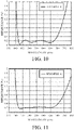
- FIG. 10 indicates a reflectance characteristic of the optical element in this example.
- a horizontal axis represents wavelength (nm) and a vertical axis represents reflectance (%). The reflectance is 0.3% or less in a wavelength range of 420 to 680 nm, which is a very good characteristic.
- a transparent resin substrate 200 in an Example 10 is made from COP resin (Zeon Corporation, "ZEONEX").
- layers 11, 13, 15, 01, and 03 use SiO 2 including Al at a weight ratio of 4.5%
- layers 12, 14, and 16 use mixture of Ta 2 O 5 and TiO 2
- a layer 02 uses MgF 2 .
- Table 10 indicates details of a film configuration of the optical element in this example.
- a refractive index and a film thickness of each material satisfy the expressions (1), (2), and (3).
- FIG. 11 indicates a reflectance characteristic of the optical element in this example.
- a horizontal axis represents wavelength (nm) and a vertical axis represents reflectance (%). The reflectance is 0.3% or less in a wavelength range of 420 to 680 nm, which is a very good characteristic.
- a transparent resin substrate 200 in an Example 11 is made from COP resin (Zeon Corporation, "ZEONEX").
- layers 12, 14, 01, and 03 use SiO 2 including Al at a weight ratio of 5.2%
- layers 11, 13, and 15 use mixture of Ta 2 O 5 and TiO 2
- a layer 02 uses MgF 2 .
- Table 11 indicates details of a film configuration of the optical element in this example.
- a refractive index and a film thickness of each material satisfy the expressions (1), (2), and (3).
- FIG. 12 indicates a reflectance characteristic of the optical element in this example.
- a horizontal axis represents wavelength (nm) and a vertical axis represents reflectance (%). The reflectance is 0.3% or less in a wavelength range of 420 to 680 nm, which is a very good characteristic.
- a transparent resin substrate 200 in an Example 12 is made from special PC resin (Mitsubishi Gas Chemical Company, Inc., "EP-5000").
- layers 11, 13, 15, 01, and 03 use SiO 2 including Al at a weight ratio of 4.5%
- layers 12, 14, and 16 use mixture of Ta 2 O 5 and TiO 2
- a layer 02 uses MgF 2 .
- Table 12 indicates details of a film configuration of the optical element in this example.
- a refractive index and a film thickness of each material satisfy the expressions (1), (2), and (3).
- FIG. 13 indicates a reflectance characteristic of the optical element in this example.
- a horizontal axis represents wavelength (nm) and a vertical axis represents reflectance (%). The reflectance is 0.3% or less in a wavelength range of 420 to 680 nm, which is a very good characteristic.
- a transparent resin substrate 200 in an Example 13 is made from special PC resin (Mitsubishi Gas Chemical Company, Inc., "EP-5000").
- layers 12, 14, 01, and 03 use SiO 2 including Al at a weight ratio of 10.0%
- layers 11, 13, and 15 use mixture of Ta 2 O 5 and TiO 2
- a layer 02 uses MgF 2 .
- Table 13 indicates details of a film configuration of the optical element in this example.
- a refractive index and a film thickness of each material satisfy the expressions (1), (2), and (3).
- FIG. 14 indicates a reflectance characteristic of the optical element in this example.
- a horizontal axis represents wavelength (nm) and a vertical axis represents reflectance (%). The reflectance is 0.3% or less in a wavelength range of 420 to 680 nm, which is a very good characteristic.
- a transparent resin substrate 200 in an Example 14 is made from polyester film (PET resin) (Toray Industries, Inc., "Lumirror T60").
- PET resin polyester film
- layers 11, 13, 15, 01, and 03 use SiO 2 including Al at a weight ratio of 5.2%
- layers 12, 14, and 16 use mixture of Ta 2 O 5 and TiO 2
- a layer 02 uses MgF 2 .
- Table 14 indicates details of a film configuration of the optical element in this example.
- a refractive index and a film thickness of each material satisfy the expressions (1), (2), and (3).
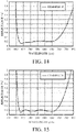
- FIG. 15 indicates a reflectance characteristic of the optical element in this example.
- a horizontal axis represents wavelength (nm) and a vertical axis represents reflectance (%). The reflectance is 0.25% or less in a wavelength range of 420 to 680 nm, which is a very good characteristic.
- a transparent resin substrate 200 in an Example 15 is made from polyester film (PET resin) (Toray Industries, Inc., "Lumirror T60").
- PET resin polyester film
- layers 11, 13, 15, 01, and 03 use SiO 2 including Al at a weight ratio of 5.2%
- layers 12, 14, and 16 use mixture of Ta 2 O 5 and TiO 2
- a layer 02 uses MgF 2 .
- Table 15 indicates details of a film configuration of the optical element in this example.
- a refractive index and a film thickness of each material satisfy the expressions (1), (2), and (3).
- FIG. 16 indicates a reflectance characteristic of the optical element in this example.
- a horizontal axis represents wavelength (nm) and a vertical axis represents reflectance (%). The reflectance is 0.3% or less in a wavelength range of 420 to 680 nm, which is a very good characteristic.
- FIG. 19 is a sectional view of an optical system 400.
- the optical system 400 includes a plurality of optical elements G401 to G411.
- a reference numeral 402 denotes a diaphragm and a reference numeral 403 denotes an image plane.
- the optical elements G401 to G411 are lenses, respectively. Of these lenses, at least one of entrance surfaces and emission surfaces is provided with the antireflection film according to any one of the Examples 1 to 15. That is, the optical system 400 includes the plurality of optical elements G401 to G411, and the plurality of optical elements G401 to G411 includes the optical element 300 provided with the antireflection film according to any one of the Examples 1 to 15.
- the optical system 400 in this Example is not limited to an image pickup optical system used in an image pickup apparatus described later, and may be applied to optical systems for various purposes such as binoculars, projectors, and telescopes.
- FIG. 20 is an external perspective view illustrating the image pickup apparatus (digital camera 500).
- the digital camera 500 includes a camera body 502 and a lens apparatus 501 which is integrally configured with the camera body 502.
- the lens apparatus 501 may be an interchangeable lens, which is detachably attachable to the camera body 502, such as a lens for a single-lens reflex camera and a lens for a mirrorless camera.
- the lens apparatus 501 includes an optical system 400 according to any one of the Examples 1 to 15.
- the camera body 502 includes an image sensor 503 such as a CMOS sensor and a CCD sensor.
- the image sensor 503 is disposed on an image plane 403 in the optical system 400.
- a Comparative Example 1 uses the same vapor deposition material, the same transparent resin substrate, and the same vapor deposition condition as those in the Example 10.
- Table 16 indicates a film configuration of an optical element in this comparative example.
- a multilayer film 101 is made only of a magnesium fluoride layer.
- FIG. 17 indicates a reflectance characteristic of the optical element in this comparative example.
- a horizontal axis represents wavelength (nm) and a vertical axis represents reflectance (%).
- the reflectance is 0.2 or less in a wavelength range of 420 to 680 nm, achieving lower reflectance than those in the Examples 1 to 15.
- Table 18 indicates the results of the durability tests.
- An outermost layer in this comparative example is made of a magnesium fluoride film having low strength. Therefore, in the configuration of this comparative example, film cracking and film peeling occur in each durability test, which is not suitable for use as an antireflection film.
- Multilayer film 101 Layer 01 MgF 2 1.38 99.3 Multilayer film 111 Layer 16 Ta 2 O 5 +TiO 2 2.00 57.2 Layer 15 SiO 2 (Al content: weight ratio 4.5%) 1.47 15.0 Layer 14 Ta 2 O 5 +TiO 2 2.00 51.0 Layer 13 SiO 2 (Al content: weight ratio 4.5%) 1.47 54.7 Layer 12 Ta 2 O 5 +TiO 2 2.00 10.0 Layer 11 SiO 2 (Al content: weight ratio 4.5%) 1.47 90.9 Resin substrate 200 COP resin 1.53 ⁇
- a Comparative Example 2 uses the same vapor deposition material, the same transparent resin substrate, and the same vapor deposition condition as those in the Example 10.
- Table 17 indicates a film configuration of an optical element in this comparative example.
- a multilayer film 101 is made only of a silicon oxide layer.
- Table 18 indicates the results of the durability tests.
- An outermost layer in this comparative example is made of a silicon oxide film having high strength. Therefore, no film cracking and no film peeling occurred in every durability test.
- FIG. 18 indicates a reflectance characteristic in this comparative example.
- a horizontal axis represents wavelength (nm) and a vertical axis represents reflectance (%).
- the reflectance is about 0.5% in a wavelength range of 420 to 680 nm, which is higher than those in the Examples 1 to 15.
- ghost and flare may be caused.
Landscapes
- Physics & Mathematics (AREA)
- Chemical & Material Sciences (AREA)
- Inorganic Chemistry (AREA)
- General Physics & Mathematics (AREA)
- Optics & Photonics (AREA)
- Engineering & Computer Science (AREA)
- Multimedia (AREA)
- Signal Processing (AREA)
- Surface Treatment Of Optical Elements (AREA)
- Laminated Bodies (AREA)
- Physical Vapour Deposition (AREA)
Abstract
Description
- The present disclosure relates to an optical element.
- Japanese Patent Application Laid-Open No. ("
JP") 2002-202401 JP 2017-134404 - However, with the configuration of the antireflection film described in
JP 2002-202401 JP 2017-134404 - The present disclosure provides an optical element, an optical system, and an optical apparatus each of which has high mechanical strength and high environmental durability.
- The present disclosure in a first aspect provides an optical element as specified in
claims 1 to 11. - The present disclosure in a second aspect provides an optical system as specified in
claim 12. - The present disclosure in a further aspect provides an optical apparatus as specified in
claim 13. - Further features of the present invention will become apparent from the following description of exemplary embodiments with reference to the attached drawings.
-
-
FIG. 1 is a schematic sectional view illustrating an optical element according to each example. -
FIG. 2 indicates a reflectance characteristic at an incident angle of 0 degree of an optical element according to an Example 1. -
FIG. 3 indicates a reflectance characteristic at an incident angle of 0 degree of an optical element according to an Example 2. -
FIG. 4 indicates a reflectance characteristic at an incident angle of 0 degree of an optical element according to an Example 3. -
FIG. 5 indicates a reflectance characteristic at an incident angle of 0 degree of an optical element according to an Example 4. -
FIG. 6 indicates a reflectance characteristic at an incident angle of 0 degree of an optical element according to an Example 5. -
FIG. 7 indicates a reflectance characteristic at an incident angle of 0 degree of an optical element according to an Example 6. -
FIG. 8 indicates a reflectance characteristic at an incident angle of 0 degree of an optical element according to an Example 7. -
FIG. 9 indicates a reflectance characteristic at an incident angle of 0 degree of an optical element according to an Example 8. -
FIG. 10 indicates a reflectance characteristic at an incident angle of 0 degree of an optical element according to an Example 9. -
FIG. 11 indicates a reflectance characteristic at an incident angle of 0 degree of an optical element according to an Example 10. -
FIG. 12 indicates a reflectance characteristic at an incident angle of 0 degree of an optical element according to an Example 11. -
FIG. 13 indicates a reflectance characteristic at an incident angle of 0 degree of an optical element according to an Example 12. -
FIG. 14 indicates a reflectance characteristic at an incident angle of 0 degree of an optical element according to an Example 13. -
FIG. 15 indicates a reflectance characteristic at an incident angle of 0 degree of an optical element according to an Example 14. -
FIG. 16 indicates a reflectance characteristic at an incident angle of 0 degree of an optical element according to an Example 15. -
FIG. 17 indicates a reflectance characteristic at an incident angle of 0 degree of an optical element according to a Comparative Example 1. -
FIG. 18 indicates a reflectance characteristic at an incident angle of 0 degree of an optical element according to a Comparative Example 2. -
FIG. 19 is a sectional view illustrating an optical system according to an Example 16. -
FIG. 20 is an external perspective view illustrating an image pickup apparatus according to an Example 17. - Referring now to the accompanying drawings, a detailed description will be given of embodiments according to the present disclosure.
- First, a description will be given of a schematic configuration of an
optical element 300 in this embodiment with reference toFIG. 1. FIG. 1 is a schematic sectional view illustrating theoptical element 300. Theoptical element 300 includes atransparent resin substrate 200 which is a base material consisting of resin material, and anantireflection film 100 formed on thetransparent resin substrate 200. Theantireflection film 100 includes amultilayer film 111 as a first film and amultilayer film 101 as a second film, in order from the side closer to thetransparent resin substrate 200. That is, theantireflection film 100 consists of amultilayer film 111 formed on thetransparent resin substrate 200 and amultilayer film 101 formed on themultilayer film 111, i.e., formed at a position farthest from thetransparent resin substrate 200. - The
multilayer film 111 consists oflayers transparent resin substrate 200. In this embodiment, themultilayer film 111 consists of six layers, but the present disclosure is not limited to this. The number of layers of themultilayer film 111 may be any number as long as themultilayer film 111 consists of one or more layer. Themultilayer film 101 consists of three layers of alayer 01 as a first layer, alayer 02 as a second layer, and alayer 03 as a third layer, in order from the side closer to themultilayer film 111. Thelayers multilayer film 101 each include silicon oxide (SiO2), and thelayer 02 includes magnesium fluoride (MgF2). More specifically, thelayers layer 02 consists of magnesium fluoride or includes magnesium fluoride as a principal component. - When the
antireflection film 100 is vapor-deposited on thetransparent resin substrate 200, it is necessary to form films with thetransparent resin substrate 200 in a state of non-heated, or of heated at low temperature of 80 degrees or less. Magnesium fluoride vapor-deposited in the state of non-heated, or of heated at low temperature of 80 degrees or less, has low film strength and strong tensile stress. On the other hand, even when vapor-deposited in the state of non-heated, or of heated at a low temperature of 80 degrees or less, silicon oxide has high film strength and strong tensile stress. In this embodiment, a magnesium fluoride layer is sandwiched between silicon oxide layers as in the configuration of themultilayer film 101, so that the film strength can be improved and adhesion can be improved by canceling the stress. - In this embodiment, the following conditional expression (1) may be satisfied where n1, n2, and n3 respectively represent refractive indexes at a d-line of the
layers layers 
- In this embodiment, the numerical range of the conditional expression (1) may be set to that in the following conditional expression (1a).

- In the
antireflection film 100, antireflection performance is improved when the outermost layer, i.e., a top layer, is made from material having a low refractive index and an optical film thickness of the outermost layer is set to about λ/4. In this embodiment, the antireflection performance can be improved by regarding themultilayer film 101 as a layer substantially equivalent to the low refractive index material of the outermost layer and satisfying the conditional expression (1). - In this embodiment, the following conditional expressions (2) and (3) may be satisfied.


- In this embodiment, the numerical ranges of the conditional expressions (2) and (3) may be set to those in the following conditional expressions (2a) and (3a).


- If the film thickness of the
layer 02 of themultilayer film 101 increases, an average refractive index of themultilayer film 101 decreases, but the film strength decreases, and tensile stress increases and makes it difficult to ensure adhesion. On the other hand, if the film thicknesses of thelayers multilayer film 101 increases. When the films are formed so that the respective film thicknesses satisfy the conditional expressions (2) and (3), it is possible to ensure both antireflection performance and film strength. - The
transparent resin substrate 200 expands as the temperature rises. Magnesium fluoride has a large tensile stress. Generally, vapor-deposited films made from silicon oxide have compressive stress, but stronger compressive stress is required to offset the stress of magnesium fluoride. In this embodiment, the compressive stress is enhanced by using silicon oxide material including a small amount of aluminum. Therefore, material forming thelayers 

- Each of the
layers - The
multilayer film 111 may be a combination of high refractive index material and medium refractive index material, which has a refractive index at the d-line of about 1.6 to 1.8, but may be a layer (alternate layer) formed by alternately laminating high refractive index material and low refractive index material. The high refractive index material used in themultilayer film 111 may be one of tantalum oxide, titanium oxide, lanthanum oxide, and zirconium oxide, or may be material whose principal component is a mixture of more than one of them. The high refractive index material has tensile stress. The low refractive index material used in themultilayer film 111 may be the same material as thelayers antireflection film 100. Since the high refractive index material has the tensile stress and the low refractive index material has the compressive stress, the stress is offset by forming the alternate layer. The alternate layer is not limited to the six layers as illustrated inFIG. 1 , as long as the alternate layer includes at least one layer for each of two types of layers made from material different from each other. - A
layer 11 which is a bottom layer of themultilayer film 111 may be made from the same material as thelayers transparent resin substrate 200 generally has a thermal expansion coefficient larger than that of glass. When material having strong compressive stress is used on thetransparent resin substrate 200, thelayer 11 can follow a shape variation of thetransparent resin substrate 200 expanding due to high temperature, and hindering film cracking from occurring. - A film forming method for the
antireflection film 100 consisting of themultilayer film 111 and themultilayer film 101 is not particularly limited as long as it is physical vapor deposition such as vapor deposition, a sputtering method, and an ion plating method. In particular, vapor deposition may be used because fluoride is less likely to decompose. In vapor deposition, heating methods for vapor deposition material include electrical resistance heating, electron-beam physical vapor deposition, pulsed laser deposition, and the like. Electron-beam physical vapor deposition may be used because it can form a film with a substrate in a non-heated state by directly heating film material, and can provide a film of relatively high quality with small amount of contamination. An ion beam assist method may also be used. By an independent ion source playing a role of assisting vapor deposition, it is possible to form a dense film with low absorption and scattering and high strength. - In this embodiment, the following conditional expression (6) may be satisfied where nd represents a refractive index (average refractive index at the d-line) of the
transparent resin substrate 200.
- Further, in this embodiment, the following conditional expression (7) may be satisfied where α (10-5/°C) represents a coefficient of linear expansion of the
transparent resin substrate 200.
- A detailed description will be given below of each example.
-
FIG. 1 is a schematic sectional view of anoptical element 300 in an Example 1 of the present disclosure. Theoptical element 300 in this example is an optical element in which anantireflection film 100 is formed on atransparent resin substrate 200. Thetransparent resin substrate 200 is made from COP resin (Zeon Corporation, "ZEONEX") having a refractive index of 1.53 (at the d-line). As layer material, layers 11, 13, 15, 01, and 03 use SiO2, layers 12, 14, and 16 use mixture of ZrO2 and TiO2, and alayer 02 uses MgF2. Table 1 indicates details of a film configuration of the optical element in this example. A refractive index and a film thickness of each material satisfy the expressions (1), (2), and (3). - A film forming method for the
antireflection film 100 in this example is as follows. Theantireflection film 100 is formed by vapor deposition. An electron beam was used to heat evaporation material. Ion beam-assisted vapor deposition was performed to form a denser film. The inside of a vacuum chamber of a vapor deposition apparatus was exhausted in a non-heated state up to a high-vacuum range of about 2×10⁻³ (Pa). After it was ensured that the inside of the vacuum chamber was in the high vacuum state, Ar as inert gas was introduced into an ion gun and the ion gun was discharged. After the ion gun became a stable state, oxygen was introduced into the vacuum chamber, and ion assisted vapor deposition using oxygen ion was performed at a vacuum pressure of about 1×10⁻² (Pa). -
FIG. 2 indicates a reflectance characteristic of the optical element in this example. InFIG. 2 , a horizontal axis represents wavelength (nm) and a vertical axis represents reflectance (%). The reflectance is 0.25% or less in a wavelength range of 420 to 680 nm, which is a very good characteristic. - The
layer 02 made from magnesium fluoride is formed by non-heating vapor deposition, and has low strength and strong tensile stress. On the other hand, a layer of silicon oxide formed by non-heating vapor deposition has high strength and has compressive stress. Themultilayer film 101 with magnesium fluoride film sandwiched between silicon oxide films as a whole has a structure in which strength is high and stress is offset, and is a film with good environmental reliability that does not cause cracking or peeling. - The
antireflection film 100 was subjected to the following durability tests for confirming its durability under various conditions. - A prepared sample was left for 1000 hours in a constant temperature bath set to a temperature of 60 degrees and a humidity of 90%, and thereafter the appearance of the
antireflection film 100 was visually observed. - A prepared sample was left for 1000 hours in a constant temperature bath set to a temperature of ―30 degrees, and thereafter the appearance of the
antireflection film 100 was visually observed. - A prepared sample was left for 12 hours in a constant temperature bath set to 70 degrees, and thereafter the appearance of the
antireflection film 100 was visually observed. - Adhesive tape was put on a surface of the
antireflection film 100 of a prepared sample, and the tape was peeled off in a direction perpendicular to the film surface. It was repeated five times and whether or not the film had peeled off was confirmed by visual observation. - After the
antireflection film 100 was rubbed for ten times back and forth with a lens-cleaning paper soaked with solvent with a load of about 200 g applied, the appearance of theantireflection film 100 was visually observed. - Table 18 indicates the results of the durability tests. It could be confirmed that no film cracking or film peeling occurred in every test, and that a good antireflection film was formed.
TABLE 1 Refractive index (d-line) Physical film thickness (nm) Multilayer film 101Layer 03SiO2 1.45 20.0 Layer 02MgF2 1.38 58.3 Layer 01SiO2 1.45 20.0 Multilayer film 111Layer 16ZrO2+TiO2 2.00 56.6 Layer 15SiO2 1.45 15.0 Layer 14ZrO2+TiO2 2.00 53.7 Layer 13SiO2 1.45 51.2 Layer 12ZrO2+TiO2 2.00 15.5 Layer 11SiO2 1.45 54.6 Resin substrate 200COP resin 1.53 ― - An optical element in an Example 2 is made by using the same transparent resin substrate, the same vapor deposition material, and the same vapor deposition condition as those in the Example 1. Table 2 indicates details of a film configuration of the optical element in this example. A refractive index and a film thickness of each material satisfy the expressions (1), (2), and (3).
FIG. 3 indicates a reflectance characteristic of the optical element in this example. InFIG. 3 , a horizontal axis represents wavelength (nm) and a vertical axis represents reflectance (%). The reflectance is 0.25% or less in a wavelength range of 420 to 680 nm, which is a very good characteristic. - Table 18 indicates the results of the durability tests. It could be confirmed that no film cracking or film peeling occurred in every test, and that a good antireflection film was formed.
TABLE 2 Refractive index (d-line) Physical film thickness (nm) Multilayer film 101Layer 03SiO2 1.45 20.0 Layer 02MgF2 1.38 59.0 Layer 01SiO2 1.45 20.0 Multilayer film 111Layer 15ZrO2+TiO2 2.00 50.3 Layer 14SiO2 1.45 15.0 Layer 13ZrO2+TiO2 2.00 57.8 Layer 12SiO2 1.45 37.3 Layer 11ZrO2+TiO2 2.00 15.4 Resin substrate 200COP resin 1.53 ― - A
transparent resin substrate 200 in an Example 3 is made from special PC resin (Mitsubishi Gas Chemical Company, Inc., "EP-5000"). As layer material, layers 11, 13, 15, 01, and 03 use SiO2 including Al at a weight ratio of 0.001%, layers 12, 14, and 16 use mixture of Ta2O5 and TiO2, and alayer 02 uses MgF2. Table 3 indicates details of a film configuration of the optical element in this example. A refractive index and a film thickness of each material satisfy the expressions (1), (2), and (3). A film forming method for anantireflection film 100 in this example is electron-beam physical vapor deposition and ion-assisted vapor deposition as in the Example 1.FIG. 4 indicates a reflectance characteristic of the optical element in this example. InFIG. 4 , a horizontal axis represents wavelength (nm) and a vertical axis represents reflectance (%). The reflectance is 0.25% or less in a wavelength range of 420 to 680 nm, which is a very good characteristic. - Table 18 indicates the results of the durability tests. It could be confirmed that no film cracking or film peeling occurred in every test, and that a good antireflection film was formed.
- In this example, the
layer 01 and thelayer 03 are SiO2 layers each including Al at the weight ratio of 0.001%. These layers have very strong compressive stress. MgF2 has very strong tensile stress, and resin material is very likely to expand. According to this example, these stresses are offset, and thus it is possible to provide an antireflection film having a very high environmental durability.TABLE 3 Refractive index (d-line) Physical film thickness (nm) Multilayer film 101Layer 03SiO2 (Al content: weight ratio 0.001%) 1.45 20.0 Layer 02MgF2 1.38 60.9 Layer 01SiO2 (Al content weight ratio 0.001%) 1.45 18.0 Multilayer film 111Layer 16Ta2O5+TiO2 2.00 55.9 Layer 15SiO2 (Al content weight ratio 0.001%) 1.45 15.0 Layer 14Ta2O5+ TiO 2200 57.7 Layer 13SiO2 (Al content weight ratio 0.001%) 1.45 471 Layer 12Ta2O5+TiO2 2.00 22.4 Layer 11SiO2 (Al content: weight ratio 0.001%) 1.45 388 Resin substrate 200Special PC 1.64 ― - A
transparent resin substrate 200 in an Example 4 is made from special PC resin (Mitsubishi Gas Chemical Company, Inc., "EP-5000"). As layer material, layers 12, 14, 01, and 03 use SiO2 including Al at a weight ratio of 1.0%, layers 11, 13, and 15 use mixture of ZrO2 and TiO2, and alayer 02 uses MgF2. Table 4 indicates details of a film configuration of the optical element in this example. A refractive index and a film thickness of each material satisfy the expressions (1), (2), and (3).FIG. 5 indicates a reflectance characteristic of the optical element in this example. InFIG. 5 , a horizontal axis represents wavelength (nm) and a vertical axis represents reflectance (%). The reflectance is 0.3% or less in a wavelength range of 420 to 680 nm, which is a very good characteristic. - Table 18 indicates the results of the durability tests. It could be confirmed that no film cracking or film peeling occurred in every test, and that a good antireflection film was formed.
TABLE 4 Refractive index (d-line) Physical film thickness (nm) Multilayer film 101Layer 03SiO2 (Al content: weight ratio 1.0%) 1.45 18.0 Layer 02MgF2 1.38 62.1 Layer 01SiO2 (Al content: weight ratio 1.0%) 1.45 20.0 Multilayer film 111Layer 15ZrO2+ TiO 2200 47.1 Layer 14SiO2 (Al content: weight ratio 1.0%) 1.45 15.0 Layer 13ZrO2+TiO2 20.0 61.7 Layer 12SiO2 (Al content: weight ratio 1.0%) 1.45 27.8 Layer 11ZrO2+TiO2 2.00 17.5 Resin substrate 200Special PC 1.64 ― - A
transparent resin substrate 200 in an Example 5 is made from COP resin (Zeon Corporation, "ZEONEX"). As layer material, layers 11, 13, 15, 01, and 03 use SiO2 including Al at a weight ratio of 2.0%, layers 12, 14, and 16 use mixture of Ta2O5 and TiO2, and alayer 02 uses MgF2. Table 5 indicates details of a film configuration of the optical element in this example. A refractive index and a film thickness of each material satisfy the expressions (1), (2), and (3).FIG. 6 indicates a reflectance characteristic of the optical element in this example. InFIG. 6 , a horizontal axis represents wavelength (nm) and a vertical axis represents reflectance (%). The reflectance is 0.25% or less in a wavelength range of 420 to 680 nm, which is a very good characteristic. - Table 18 indicates the results of the durability tests. It could be confirmed that no film cracking or film peeling occurred in every test, and that a good antireflection film was formed.
TABLE 5 Refractive index (d-line) Physical film thickness (nm) Multilayer film 101Layer 03SiO2 (Al content: weight ratio 2.0%) 1.46 19,5 Layer 02MgF2 1.38 55.9 Layer 01SiO2 (Al content: weight ratio 2.0%) 1.46 23.0 Multilayer film 111Layer 16Ta2O5+TiO2 2.00 56.4 Layer 15SiO2 (Al content: weight ratio 2.0%) 1.46 15.0 Layer 14Ta2O5+TiO2 2.00 53.6 Layer 13SiO2 (Al content: weight ratio 2.0%) 1.46 51.0 Layer 12Ta2O5+TiO2 2.00 15.0 Layer 11SiO2 (Al content: weight ratio 2.0%) 1.46 53.8 Resin substrate 200COP resin 1.53 ― - A
transparent resin substrate 200 in an Example 6 is made from COP resin (Zeon Corporation, "ZEONEX"). As layer material, layers 11, 13, 15, 01, and 03 use SiO2 including Al at a weight ratio of 3.0%, layers 12, 14, and 16 use mixture of Ta2O5 and TiO2, and alayer 02 uses MgF2. Table 6 indicates details of a film configuration of the optical element in this example. A refractive index and a film thickness of each material satisfy the expressions (1), (2), and (3).FIG. 7 indicates a reflectance characteristic of the optical element in this example. InFIG. 7 , a horizontal axis represents wavelength (nm) and a vertical axis represents reflectance (%). The reflectance is 0.3% or less in a wavelength range of 420 to 680 nm, which is a very good characteristic. - Table 18 indicates the results of the durability tests. It could be confirmed that no film cracking or film peeling occurred in every test, and that a good antireflection film was formed.
TABLE 6 Refractive index (d-line) Physical film thickness (nm) Multilayer film 101Layer 03SiO2 (Al content: weight ratio 3.0%) 1,46 29.0 Layer 02MgF2 1.38 402 Layer 01SiO2 (Al content: weight ratio 3.0%) 1.46 27.5 Multilayer film 111Layer 16Ta2O5+TiO2 2.00 59.5 Layer 15SiO2 (Al content: weight ratio 3.0%) 1.46 15.0 Layer 14Ta2O5+TiO2 2.00 51.5 Layer 13SiO2 (Al content: weight ratio 3.0%) 1.46 52.0 Layer 12Ta2O5+TiO2 2.00 150 Layer 11SiO2 (Al content: weight ratio 3.0%) 1.46 51.1 Resin substrate 200COP resin 1.53 ― - A
transparent resin substrate 200 in an Example 7 is made from COP resin (Zeon Corporation, "ZEONEX"). As layer material, layers 12, 14, 01, and 03 use SiO2 including Al at a weight ratio of 2.0%, layers 11, 13, and 15 use mixture of Ta2O5 and TiO2, and alayer 02 uses MgF2. Table 7 indicates details of a film configuration of the optical element in this example. A refractive index and a film thickness of each material satisfy the expressions (1), (2), and (3).FIG. 8 indicates a reflectance characteristic of the optical element in this example. InFIG. 8 , a horizontal axis represents wavelength (nm) and a vertical axis represents reflectance (%). The reflectance is 0.3% or less in a wavelength range of 420 to 680 nm, which is a very good characteristic. - Table 18 indicates the results of the durability tests. It could be confirmed that no film cracking or film peeling occurred in every test, and that a good antireflection film was formed.
TABLE 7 Refractive index (d-line) Physical film thickness (nm) Multilayer film 101Layer 03SiO2 (Al content: weight ratio 2.0%) 1.46 25.0 Layer 02MgF2 1.38 57.1 Layer 01SiO2 (Al content: weight ratio 2.0%) 1.46 15.0 Multilayer film 111Layer 15Ta2O5+TiO2 2.00 52.1 Layer 14SiO2 (Al content: weight ratio 2.0%) 1.46 15.0 Layer 13Ta2O5+TiO2 2.00 57.3 Layer 12SiO2 (Al content: weight ratio 2.0%) 1.46 39.1 Layer 11Ta2O5+TiO2 2.00 15.0 Resin substrate 200COP resin 1.53 - A
transparent resin substrate 200 in an Example 8 is made from special PC resin (Mitsubishi Gas Chemical Company, Inc., "EP-5000"). As layer material, layers 11, 13, 15, 01, and 03 use SiO2 including Al at a weight ratio of 3.0%, layers 12, 14 and, 16 use mixture of Ta2O5 and TiO2, and alayer 02 uses MgF2. Table 8 indicates details of a film configuration of the optical element in this example. A refractive index and a film thickness of each material satisfy the expressions (1), (2), and (3).FIG. 9 indicates a reflectance characteristic of the optical element in this example. InFIG. 9 , a horizontal axis represents wavelength (nm) and a vertical axis represents reflectance (%). The reflectance is 0.25% or less in a wavelength range of 420 to 680 nm, which is a very good characteristic. - Table 18 indicates the results of the durability tests. It could be confirmed that no film cracking or film peeling occurred in every test, and that a good antireflection film was formed.
TABLE 8 Refractive index (d-line) Physical film thickness (nm) Multilayer film 101Layer 03SiO2 (Al content: weight ratio 3.0%) 1.46 20.0 Layer 02MgF2 1.38 60.9 Layer 01SiO2 (Al content: weight ratio 3.0%) 1.46 18.0 Multilayer film 111Layer 16Ta2O5+TiO2 2.00 55.9 Layer 15SiO2 (Al content: weight ratio 3.0%) 1.46 15.0 Layer 14Ta2O5+TiO2 2.00 57.7 Layer 13SiO2 (Al content: weight ratio 3.0%) 1.46 47.1 Layer 12Ta2O5+TiO2 2.00 22.4 Layer 11SiO2 (Al content: weight ratio 3.0%) 1.46 388 Resin substrate 200Special PC 1.64 ― - A
transparent resin substrate 200 in an Example 9 is made from special PC resin (Mitsubishi Gas Chemical Company, Inc., "EP-5000"). As layer material, layers 11, 13, 15, 01, and 03 use SiO2 including Al at a weight ratio of 2.5%, layers 12, 14, and 16 use mixture of Ta2O5 and TiO2, and alayer 02 uses MgF2. Table 9 indicates details of a film configuration of the optical element in this example. A refractive index and a film thickness of each material satisfy the expressions (1), (2), and (3).FIG. 10 indicates a reflectance characteristic of the optical element in this example. InFIG. 10 , a horizontal axis represents wavelength (nm) and a vertical axis represents reflectance (%). The reflectance is 0.3% or less in a wavelength range of 420 to 680 nm, which is a very good characteristic. - Table 18 indicates the results of the durability tests. It could be confirmed that no film cracking or film peeling occurred in every test, and that a good antireflection film was formed.
TABLE 9 Refractive index (d-line) Physical film thickness (nm) Multilayer film 101Layer 03SiO2 (Al content: weight ratio 2.5%) 1.46 15.0 Layer 02MgF2 1.38 67.7 Layer 01SiO2 (Al content: weight ratio 2.5%) 1.46 12.0 Multilayer film 111Layer 16Ta2O5+TiO2 2.00 59.8 Layer 15SiO2 (Al content: weight ratio 2.5%) 1.46 150 Layer 14Ta2O5+TiO2 2.00 521 Layer 13SiO2 (Al content: weight ratio 2.5%) 1.46 63.9 Layer 12Ta2O5+TiO2 2.00 15.0 Layer 11SiO2 (Al content: weight ratio 2.5%) 1.46 595 Resin substrate 200Special PC 1.64 ― - A
transparent resin substrate 200 in an Example 10 is made from COP resin (Zeon Corporation, "ZEONEX"). As layer material, layers 11, 13, 15, 01, and 03 use SiO2 including Al at a weight ratio of 4.5%, layers 12, 14, and 16 use mixture of Ta2O5 and TiO2, and alayer 02 uses MgF2. Table 10 indicates details of a film configuration of the optical element in this example. A refractive index and a film thickness of each material satisfy the expressions (1), (2), and (3).FIG. 11 indicates a reflectance characteristic of the optical element in this example. InFIG. 11 , a horizontal axis represents wavelength (nm) and a vertical axis represents reflectance (%). The reflectance is 0.3% or less in a wavelength range of 420 to 680 nm, which is a very good characteristic. - Table 18 indicates the results of the durability tests. It could be confirmed that no film cracking or film peeling occurred in every test, and that a good antireflection film was formed.
TABLE 10 Refractive index (d-line) Physical film thickness (nm) Multilayer film 101Layer 03SiO2 (Al content: weight ratio 4.5%) 1.47 20.0 Layer 02MgF2 1.38 58.1 Layer 01SiO2 (Al content: weight ratio 4.5%) 1.47 20.0 Multilayer film 111Layer 16Ta2O5+TiO2 2.00 51.5 Layer 15SiO2 (Al content: weight ratio 4.5%) 1.47 15.0 Layer 14Ta2O5+ TiO 2200 57.6 Layer 13SiO2 (Al content: weight ratio 4.5%) 1.47 42.2 Layer 12Ta2O5+ TiO 2200 16.8 Layer 11SiO2 (Al content: weight ratio 4.5%) 1.47 30.0 Resin substrate 200COP resin 1.53 ― - A
transparent resin substrate 200 in an Example 11 is made from COP resin (Zeon Corporation, "ZEONEX"). As layer material, layers 12, 14, 01, and 03 use SiO2 including Al at a weight ratio of 5.2%, layers 11, 13, and 15 use mixture of Ta2O5 and TiO2, and alayer 02 uses MgF2. Table 11 indicates details of a film configuration of the optical element in this example. A refractive index and a film thickness of each material satisfy the expressions (1), (2), and (3).FIG. 12 indicates a reflectance characteristic of the optical element in this example. InFIG. 12 , a horizontal axis represents wavelength (nm) and a vertical axis represents reflectance (%). The reflectance is 0.3% or less in a wavelength range of 420 to 680 nm, which is a very good characteristic. - Table 18 indicates the results of the durability tests. It could be confirmed that no film cracking or film peeling occurred in every test, and that a good antireflection film was formed.
TABLE 11 Refractive index (d-line) Physical film thickness (nm) Multilayer film 101Layer 03SiO2 (Al content: weight ratio 5.2%) 1.47 20.0 Layer 02MgF2 1.38 56.0 Layer 01SiO2 (Al content: weight ratio 5.2%) 1.47 20.0 Multilayer film 111Layer 15Ta2O5+TiO2 2.00 529 Layer 14SiO2 (Al content: weight ratio 5.2%) 1.47 10.0 Layer 13Ta2O5+TiO2 20.0 64.1 Layer 12SiO2 (Al content: weight ratio 5.2%) 1.47 36.0 Layer 11Ta2O5+TiO2 2.00 15.4 Resin substrate 200COP resin 1.53 ― - A
transparent resin substrate 200 in an Example 12 is made from special PC resin (Mitsubishi Gas Chemical Company, Inc., "EP-5000"). As layer material, layers 11, 13, 15, 01, and 03 use SiO2 including Al at a weight ratio of 4.5%, layers 12, 14, and 16 use mixture of Ta2O5 and TiO2, and alayer 02 uses MgF2. Table 12 indicates details of a film configuration of the optical element in this example. A refractive index and a film thickness of each material satisfy the expressions (1), (2), and (3).FIG. 13 indicates a reflectance characteristic of the optical element in this example. InFIG. 13 , a horizontal axis represents wavelength (nm) and a vertical axis represents reflectance (%). The reflectance is 0.3% or less in a wavelength range of 420 to 680 nm, which is a very good characteristic. - Table 18 indicates the results of the durability tests. It could be confirmed that no film cracking or film peeling occurred in every test, and that a good antireflection film was formed.
TABLE 12 Refractive index (d-line) Physical film thickness (nm) Multilayer film 101Layer 03SiO2 (Al content: weight ratio 4.5%) 1.47 20.0 Layer 02MgF2 1.38 56.0 Layer 01SiO2 (Al content: weight ratio 4.5%) 1.47 20.0 Multilayer film 111Layer 16Ta2O5+TiO2 2.00 55.4 Layer 15SiO2 (Al content: weight ratio 4.5%) 1.47 10.3 Layer 14Ta2O5+TiO2 2.00 60.4 Layer 13SiO2 (Al content: weight ratio 4.5%) 1.47 43.8 Layer 12Ta2O5+TiO2 2.00 20.7 Layer 11SiO2 (Al content: weight ratio 4.5%) 1.47 41.4 Resin substrate 200Special PC 1.64 ― - A
transparent resin substrate 200 in an Example 13 is made from special PC resin (Mitsubishi Gas Chemical Company, Inc., "EP-5000"). As layer material, layers 12, 14, 01, and 03 use SiO2 including Al at a weight ratio of 10.0%, layers 11, 13, and 15 use mixture of Ta2O5 and TiO2, and alayer 02 uses MgF2. Table 13 indicates details of a film configuration of the optical element in this example. A refractive index and a film thickness of each material satisfy the expressions (1), (2), and (3).FIG. 14 indicates a reflectance characteristic of the optical element in this example. InFIG. 14 , a horizontal axis represents wavelength (nm) and a vertical axis represents reflectance (%). The reflectance is 0.3% or less in a wavelength range of 420 to 680 nm, which is a very good characteristic. - Table 18 indicates the results of the durability tests. It could be confirmed that no film cracking or film peeling occurred in every test, and that a good antireflection film was formed.
TABLE 13 Refractive index (d-line) Physical film thickness (nm) Multilayer film 101Layer 03SiO2 (Al content: weight ratio 10.0%) 1.47 20.0 Layer 02MgF2 1.38 56.2 Layer 01SiO2 (Al content: weight ratio 10.0%) 1.47 20.0 Multilayer film 111Layer 15Ta2O5+TiO2 2.00 47.4 Layer 14SiO2 (Al content: weight ratio 10.0%) 1.47 10.0 Layer 13Ta2O5+TiO2 2.00 66.9 Layer 12SiO2 (Al content: weight ratio 10.0%) 1.47 27.5 Layer 11Ta2O5+TiO2 2.00 168 Resin substrate 200Special PC 1.64 ― - A
transparent resin substrate 200 in an Example 14 is made from polyester film (PET resin) (Toray Industries, Inc., "Lumirror T60"). As layer material, layers 11, 13, 15, 01, and 03 use SiO2 including Al at a weight ratio of 5.2%, layers 12, 14, and 16 use mixture of Ta2O5 and TiO2, and alayer 02 uses MgF2. Table 14 indicates details of a film configuration of the optical element in this example. A refractive index and a film thickness of each material satisfy the expressions (1), (2), and (3).FIG. 15 indicates a reflectance characteristic of the optical element in this example. InFIG. 15 , a horizontal axis represents wavelength (nm) and a vertical axis represents reflectance (%). The reflectance is 0.25% or less in a wavelength range of 420 to 680 nm, which is a very good characteristic. - Table 18 indicates the results of the durability tests. It could be confirmed that no film cracking or film peeling occurred in every test, and that a good antireflection film was formed.
TABLE 14 Refractive index (d-line) Physical film thickness (nm) Multilayer film 101Layer 03SiO2 (Al content: weight ratio 5.2%) 1.47 20.0 Layer 02MgF2 1.38 57.4 Layer 01SiO2 (Al content: weight ratio 5.2%) 1.47 20.0 Multilayer film 111Layer 16Ta2O5+TiO2 2.00 59.5 Layer 15SiO2 (Al content: weight ratio 5.2%) 1.47 15.0 Layer 14Ta2O5+TiO2 2.00 53.7 Layer 13SiO2 (Al content: weight ratio 5.2%) 1 47 53 2 Layer 12Ta2O5+TiO2 2.00 19.7 Layer 11SiO2 (Al content: weight ratio 5.2%) 1.47 44.7 Resin substrate 200PET 1 65 ― - A
transparent resin substrate 200 in an Example 15 is made from polyester film (PET resin) (Toray Industries, Inc., "Lumirror T60"). As layer material, layers 11, 13, 15, 01, and 03 use SiO2 including Al at a weight ratio of 5.2%, layers 12, 14, and 16 use mixture of Ta2O5 and TiO2, and alayer 02 uses MgF2. Table 15 indicates details of a film configuration of the optical element in this example. A refractive index and a film thickness of each material satisfy the expressions (1), (2), and (3).FIG. 16 indicates a reflectance characteristic of the optical element in this example. InFIG. 16 , a horizontal axis represents wavelength (nm) and a vertical axis represents reflectance (%). The reflectance is 0.3% or less in a wavelength range of 420 to 680 nm, which is a very good characteristic. - Table 18 indicates the results of the durability tests. It could be confirmed that no film cracking or film peeling occurred in every test, and that a good antireflection film was formed.
TABLE 15 Refractive index (d-line) Physical film thickness (nm) Multilayer film 101Layer 03SiO2 (Al content: weight ratio 5.2%) 1.47 30.0 Layer 02MgF2 1.38 35.4 Layer 01SiO2 (Al content: weight ratio 5.2%) 1.47 28.0 Multilayer film 111Layer 16Ta2O5+TiO2 2.00 70.2 Layer 15SiO2 (Al content: weight ratio 5.2%) 1.47 15.1 Layer 14Ta2O5+TiO2 2.00 43.8 Layer 13SiO2 (Al content: weight ratio 5.2%) 1.47 65.4 Layer 12Ta2O5+TiO2 2.00 15.0 Layer 11SiO2 (Al content: weight ratio 5.2%) 1.47 51.6 Resin substrate 200PET 1.65 ― - Next, a description will be given of an optical system in an Example 16 with reference to
FIG. 19. FIG. 19 is a sectional view of anoptical system 400. Theoptical system 400 includes a plurality of optical elements G401 to G411. Areference numeral 402 denotes a diaphragm and areference numeral 403 denotes an image plane. The optical elements G401 to G411 are lenses, respectively. Of these lenses, at least one of entrance surfaces and emission surfaces is provided with the antireflection film according to any one of the Examples 1 to 15. That is, theoptical system 400 includes the plurality of optical elements G401 to G411, and the plurality of optical elements G401 to G411 includes theoptical element 300 provided with the antireflection film according to any one of the Examples 1 to 15. - The
optical system 400 in this Example is not limited to an image pickup optical system used in an image pickup apparatus described later, and may be applied to optical systems for various purposes such as binoculars, projectors, and telescopes. - Next, a description will be given of an image pickup apparatus in an Example 17 with reference to
FIG. 20. FIG. 20 is an external perspective view illustrating the image pickup apparatus (digital camera 500). - The
digital camera 500 includes acamera body 502 and alens apparatus 501 which is integrally configured with thecamera body 502. However, this example is not limited to this, and thelens apparatus 501 may be an interchangeable lens, which is detachably attachable to thecamera body 502, such as a lens for a single-lens reflex camera and a lens for a mirrorless camera. Thelens apparatus 501 includes anoptical system 400 according to any one of the Examples 1 to 15. Thecamera body 502 includes animage sensor 503 such as a CMOS sensor and a CCD sensor. Theimage sensor 503 is disposed on animage plane 403 in theoptical system 400. - A Comparative Example 1 uses the same vapor deposition material, the same transparent resin substrate, and the same vapor deposition condition as those in the Example 10. Table 16 indicates a film configuration of an optical element in this comparative example. A
multilayer film 101 is made only of a magnesium fluoride layer.FIG. 17 indicates a reflectance characteristic of the optical element in this comparative example. InFIG. 17 , a horizontal axis represents wavelength (nm) and a vertical axis represents reflectance (%). The reflectance is 0.2 or less in a wavelength range of 420 to 680 nm, achieving lower reflectance than those in the Examples 1 to 15. - Table 18 indicates the results of the durability tests. An outermost layer in this comparative example is made of a magnesium fluoride film having low strength. Therefore, in the configuration of this comparative example, film cracking and film peeling occur in each durability test, which is not suitable for use as an antireflection film.
TABLE 16 Refractive index (d-line) Physical film thickness (nm) Multilayer film 101Layer 01MgF2 1.38 99.3 Multilayer film 111Layer 16Ta2O5+TiO2 2.00 57.2 Layer 15SiO2 (Al content: weight ratio 4.5%) 1.47 15.0 Layer 14Ta2O5+TiO2 2.00 51.0 Layer 13SiO2 (Al content: weight ratio 4.5%) 1.47 54.7 Layer 12Ta2O5+TiO2 2.00 10.0 Layer 11SiO2 (Al content: weight ratio 4.5%) 1.47 90.9 Resin substrate 200COP resin 1.53 ― - A Comparative Example 2 uses the same vapor deposition material, the same transparent resin substrate, and the same vapor deposition condition as those in the Example 10. Table 17 indicates a film configuration of an optical element in this comparative example. A
multilayer film 101 is made only of a silicon oxide layer. - Table 18 indicates the results of the durability tests. An outermost layer in this comparative example is made of a silicon oxide film having high strength. Therefore, no film cracking and no film peeling occurred in every durability test.
-
FIG. 18 indicates a reflectance characteristic in this comparative example. InFIG. 18 , a horizontal axis represents wavelength (nm) and a vertical axis represents reflectance (%). The reflectance is about 0.5% in a wavelength range of 420 to 680 nm, which is higher than those in the Examples 1 to 15. Thus, in the configuration of this comparative example, ghost and flare may be caused.TABLE 17 Refractive index (d-line) Physical film thickness (mm) Multilayer film 101 Layer 01 SiO2(Al content: weight ratio 4,5%) 1.47 92.6 Multilayer film 111 Layer 16 Ta2O5+TiO2 2.00 69.9 Layer 15 SiO2(Al content: weight ratio 4.5%) 1.47 15.0 Layer 14 Ta2O5+TiO2 2.00 43.7 Layer 13 SiO2(Al content: weight ratio 4.5%) 1.47 55.3 Layer 12 Ta2O5+TiO2 2.00 12.5 Layer 11 SiO2(Al content: weight ratio 4.5%) 1.47 57.6 Resin substrate 200 COP resin 1.53 - TABLE 18 Antireflection Effect High-temperature/humidity shelf test Low-temperature shelf test High-temperature shelf test Adhesion test Surface hardness test Ex.1 ○ ○ ○ ○ ○ ○ Ex.2 ○ ○ ○ ○ ○ ○ Ex.3 ○ ○ ○ ○ ○ ○ Ex.4 ○ ○ ○ ○ ○ ○ Ex.5 ○ ○ ○ ○ ○ ○ Ex.6 ○ ○ ○ ○ ○ ○ Ex.7 ○ ○ ○ ○ ○ ○ Ex.8 ○ ○ ○ ○ ○ ○ Ex.9 ○ ○ ○ ○ ○ ○ Ex.10 ○ ○ ○ ○ ○ ○ Ex.11 ○ ○ ○ ○ ○ ○ Ex.12 ○ ○ ○ ○ ○ ○ Ex.13 ○ ○ ○ ○ ○ ○ Ex.14 ○ ○ ○ ○ ○ ○ Ex.15 ○ ○ ○ ○ ○ ○ Comparative Ex. 1 
crack appeared crack appeared crack appeared film peeled film peeled Comparative Ex. 2 × ○ ○ ○ ○ ○ - According to each example, it is possible to provide an optical element, an optical system, and an optical apparatus each of which has high mechanical strength and high environmental durability.
- While the present invention has been described with reference to exemplary embodiments, it is to be understood that the invention is not limited to the disclosed exemplary embodiments. The scope of the following claims is to be accorded the broadest interpretation so as to encompass all such modifications and equivalent structures and functions.
Claims (13)
- An optical element (300) comprising a base material (200), which consists of resin material, and an antireflection film (100),characterized in that the antireflection film (100) consists of a first film (111) formed on the base material (200) and a second film (101) formed on the first film (111),wherein the second film (101) consists of a first layer (01), a second layer (02), and a third layer (03), in order from a side closest to the first film (111),wherein the first layer (01) and the third layer (03) each include silicon oxide, andwherein the second layer (02) includes magnesium fluoride.
- The optical element according to claim 1,wherein a following conditional expression is satisfied:
 where n1 represents a refractive index at a d-line of the first layer, n2 represents a refractive index at the d-line of the second layer, n3 represents a refractive index at the d-line of the third layer, d1 (nm) represents a physical film thickness of the first layer, d2 (nm) represents a physical film thickness of the second layer, d3 (nm) represents a physical film thickness of the third layer, and λ (nm) represents a wavelength of the d-line.
 - The optical element according to claim 2,
wherein a following conditional expression is satisfied:
- The optical element according to any one of claims 1 to 3,wherein following conditional expressions are satisfied:

 where n1 represents a refractive index at a d-line of the first layer, n2 represents a refractive index at the d-line of the second layer, n3 represents a refractive index at the d-line of the third layer, d1 (nm) represents a physical film thickness of the first layer, d2 (nm) represents a physical film thickness of the second layer, and d3 (nm) represents a physical film thickness of the third layer.
 - The optical element according to claim 4,
wherein following conditional expressions are satisfied:

- The optical element according to any one of claims 1 to 5,wherein following conditional expressions are satisfied:

 where n1 represents a refractive index at a d-line of the first layer, and n3 represents a refractive index at the d-line of the third layer.
 - The optical element according to any one of claims 1 to 6,
wherein the first layer and the third layer each include silicon oxide at a weight ratio of 90% or more. - The optical element according to claim 7,
wherein the first layer and the third layer each include aluminum at a weight ratio of 10% or less. - The optical element according to any one of claims 1 to 8, wherein the first film is formed by alternately laminating:material included in each of the first layer and the third layer of the second film; andmaterial including at least one of tantalum oxide, titanium oxide, lanthanum oxide, and zirconium oxide.
- The optical element according to any one of claims 1 to 9,wherein a following conditional expression is satisfied:
 where nd represents an average refractive index at a d-line of the resin material.
 - The optical element according to any one of claims 1 to 10,wherein a following conditional expression is satisfied:
 where α (10-5/°C) represents a coefficient of a linear expansion of the resin material.
 - An optical system (400) comprising a plurality of optical elements (G401-G411),
characterized in that the plurality of optical elements (G401-G411) include the optical element (300) according to any one of claims 1 to 11. - An optical apparatus (500) comprising:an image sensor (503); andthe optical element (300) according to any one of claims 1 to 11.
Applications Claiming Priority (1)
| Application Number | Priority Date | Filing Date | Title |
|---|---|---|---|
| JP2020181840A JP7599910B2 (en) | 2020-10-29 | 2020-10-29 | Optical element, optical system, and optical device |
Publications (2)
| Publication Number | Publication Date |
|---|---|
| EP3992672A1 true EP3992672A1 (en) | 2022-05-04 |
| EP3992672B1 EP3992672B1 (en) | 2024-09-04 |
Family
ID=78483124
Family Applications (1)
| Application Number | Title | Priority Date | Filing Date |
|---|---|---|---|
| EP21202894.8A Active EP3992672B1 (en) | 2020-10-29 | 2021-10-15 | Optical element, optical system, and optical apparatus |
Country Status (3)
| Country | Link |
|---|---|
| US (1) | US12164081B2 (en) |
| EP (1) | EP3992672B1 (en) |
| JP (1) | JP7599910B2 (en) |
Families Citing this family (1)
| Publication number | Priority date | Publication date | Assignee | Title |
|---|---|---|---|---|
| WO2024043120A1 (en) * | 2022-08-24 | 2024-02-29 | Agc株式会社 | Dielectric multilayer film-equipped substrate and method for manufacturing same |
Citations (5)
| Publication number | Priority date | Publication date | Assignee | Title |
|---|---|---|---|---|
| EP0382477A1 (en) * | 1989-02-07 | 1990-08-16 | Tokuyama Corporation | Resin having a high refractive index |
| JP2002202401A (en) | 2000-12-28 | 2002-07-19 | Minolta Co Ltd | Reflection preventing film and plastics optical component equipped with the same |
| US20170090071A1 (en) * | 2015-09-30 | 2017-03-30 | Topcon Corporation | Antireflection film, optical element and ophthalmology apparatus |
| JP2017134404A (en) | 2016-01-25 | 2017-08-03 | キヤノン株式会社 | Optical element and method for manufacturing optical element |
| EP3660548A1 (en) * | 2018-11-26 | 2020-06-03 | Konica Minolta, Inc. | Optical member and producing method of optical member |
Family Cites Families (7)
| Publication number | Priority date | Publication date | Assignee | Title |
|---|---|---|---|---|
| JP2003098307A (en) | 2001-09-20 | 2003-04-03 | Moriroku Co Ltd | Antireflection coating on plastic optical substrate and method of forming the same |
| JP2005292462A (en) * | 2004-03-31 | 2005-10-20 | Konica Minolta Opto Inc | Optical element having dielectric multilayer film |
| JP5603714B2 (en) | 2010-09-02 | 2014-10-08 | オリンパス株式会社 | Antireflection film, lens, optical system, objective lens, and optical apparatus |
| FR3002767B1 (en) | 2013-03-01 | 2015-02-27 | Saint Gobain | VISUALIZATION DEVICE FOR TRANSPARENT GLAZING |
| CN105814003B (en) | 2013-12-16 | 2018-11-30 | Agc株式会社 | Glass with anti-reflection film and manufacturing method thereof |
| RU2684919C2 (en) | 2015-03-13 | 2019-04-16 | Рупп + Хубрах Оптик Гмбх | Optical product containing an illuminating coating in the visible area, for conditions of low illumination |
| JP6764911B2 (en) | 2018-09-27 | 2020-10-07 | 株式会社トプコン | Anti-reflective coatings, optics, and ophthalmic devices |
-
2020
- 2020-10-29 JP JP2020181840A patent/JP7599910B2/en active Active
-
2021
- 2021-10-15 EP EP21202894.8A patent/EP3992672B1/en active Active
- 2021-10-18 US US17/503,747 patent/US12164081B2/en active Active
Patent Citations (5)
| Publication number | Priority date | Publication date | Assignee | Title |
|---|---|---|---|---|
| EP0382477A1 (en) * | 1989-02-07 | 1990-08-16 | Tokuyama Corporation | Resin having a high refractive index |
| JP2002202401A (en) | 2000-12-28 | 2002-07-19 | Minolta Co Ltd | Reflection preventing film and plastics optical component equipped with the same |
| US20170090071A1 (en) * | 2015-09-30 | 2017-03-30 | Topcon Corporation | Antireflection film, optical element and ophthalmology apparatus |
| JP2017134404A (en) | 2016-01-25 | 2017-08-03 | キヤノン株式会社 | Optical element and method for manufacturing optical element |
| EP3660548A1 (en) * | 2018-11-26 | 2020-06-03 | Konica Minolta, Inc. | Optical member and producing method of optical member |
Non-Patent Citations (1)
| Title |
|---|
| ANONYMOUS: "High-refractive-index polymer - Wikipedia", 8 October 2021 (2021-10-08), XP055894483, Retrieved from the Internet <URL:https://en.wikipedia.org/wiki/High-refractive-index_polymer> [retrieved on 20220222] * |
Also Published As
| Publication number | Publication date |
|---|---|
| JP2022072420A (en) | 2022-05-17 |
| JP7599910B2 (en) | 2024-12-16 |
| EP3992672B1 (en) | 2024-09-04 |
| US20220137265A1 (en) | 2022-05-05 |
| US12164081B2 (en) | 2024-12-10 |
Similar Documents
| Publication | Publication Date | Title |
|---|---|---|
| EP3196677A1 (en) | Optical element and method for producing the same | |
| EP2962137B1 (en) | Enhanced, durable silver coating stacks for highly reflective mirrors | |
| US11143800B2 (en) | Extending the reflection bandwith of silver coating stacks for highly reflective mirrors | |
| EP2687875A1 (en) | Optical member and method for producing same | |
| JP2005292462A (en) | Optical element having dielectric multilayer film | |
| JPWO2018062298A1 (en) | Lens unit and imaging device | |
| EP3992672B1 (en) | Optical element, optical system, and optical apparatus | |
| JP3221770B2 (en) | Anti-reflection coating for plastic optical parts | |
| KR20180078328A (en) | Spectacle lenses and glasses | |
| JP5292318B2 (en) | Antireflection film and optical member having the same | |
| JP2005165249A (en) | Antireflection film, optical lens equipped therewith and optical lens unit | |
| JP7404673B2 (en) | Antireflection film, its manufacturing method, and optical components | |
| JP2003131011A (en) | Multilayer film and substrate with multilayer film using the multilayer film | |
| EP3968083B1 (en) | Plastic substrate nd filter and plastic substrate nd filter for use in eyeglasses | |
| JP2005173326A (en) | Plastic optical component | |
| JP4447393B2 (en) | Glass member with optical multilayer film, and optical element using the glass member | |
| JP2020148806A (en) | Anti-reflective coating with coating film | |
| US11643361B2 (en) | Method of increasing strength of glass substrate for optical filter and tempered-glass optical filter made thereby | |
| JP2006301487A (en) | Near-infrared ray cut filter | |
| US12386102B2 (en) | Optical element, optical system, and optical apparatus | |
| JP3361621B2 (en) | Anti-reflection coating for infrared region | |
| US20060245056A1 (en) | Thin-film structure with counteracting layer | |
| JP2022139912A (en) | Optical elements, optical systems, and optical instruments | |
| JPS58221811A (en) | Heat-resistant antireflection film | |
| JP6799850B2 (en) | Optical sheet |
Legal Events
| Date | Code | Title | Description |
|---|---|---|---|
| PUAI | Public reference made under article 153(3) epc to a published international application that has entered the european phase |
Free format text: ORIGINAL CODE: 0009012 |
|
| STAA | Information on the status of an ep patent application or granted ep patent |
Free format text: STATUS: THE APPLICATION HAS BEEN PUBLISHED |
|
| AK | Designated contracting states |
Kind code of ref document: A1 Designated state(s): AL AT BE BG CH CY CZ DE DK EE ES FI FR GB GR HR HU IE IS IT LI LT LU LV MC MK MT NL NO PL PT RO RS SE SI SK SM TR |
|
| STAA | Information on the status of an ep patent application or granted ep patent |
Free format text: STATUS: REQUEST FOR EXAMINATION WAS MADE |
|
| 17P | Request for examination filed |
Effective date: 20221104 |
|
| RBV | Designated contracting states (corrected) |
Designated state(s): AL AT BE BG CH CY CZ DE DK EE ES FI FR GB GR HR HU IE IS IT LI LT LU LV MC MK MT NL NO PL PT RO RS SE SI SK SM TR |
|
| GRAP | Despatch of communication of intention to grant a patent |
Free format text: ORIGINAL CODE: EPIDOSNIGR1 |
|
| STAA | Information on the status of an ep patent application or granted ep patent |
Free format text: STATUS: GRANT OF PATENT IS INTENDED |
|
| INTG | Intention to grant announced |
Effective date: 20240412 |
|
| GRAS | Grant fee paid |
Free format text: ORIGINAL CODE: EPIDOSNIGR3 |
|
| GRAA | (expected) grant |
Free format text: ORIGINAL CODE: 0009210 |
|
| STAA | Information on the status of an ep patent application or granted ep patent |
Free format text: STATUS: THE PATENT HAS BEEN GRANTED |
|
| AK | Designated contracting states |
Kind code of ref document: B1 Designated state(s): AL AT BE BG CH CY CZ DE DK EE ES FI FR GB GR HR HU IE IS IT LI LT LU LV MC MK MT NL NO PL PT RO RS SE SI SK SM TR |
|
| REG | Reference to a national code |
Ref country code: GB Ref legal event code: FG4D |
|
| REG | Reference to a national code |
Ref country code: CH Ref legal event code: EP |
|
| REG | Reference to a national code |
Ref country code: IE Ref legal event code: FG4D |
|
| REG | Reference to a national code |
Ref country code: DE Ref legal event code: R096 Ref document number: 602021018234 Country of ref document: DE |
|
| REG | Reference to a national code |
Ref country code: LT Ref legal event code: MG9D |
|
| REG | Reference to a national code |
Ref country code: NL Ref legal event code: MP Effective date: 20240904 |
|
| PG25 | Lapsed in a contracting state [announced via postgrant information from national office to epo] |
Ref country code: NO Free format text: LAPSE BECAUSE OF FAILURE TO SUBMIT A TRANSLATION OF THE DESCRIPTION OR TO PAY THE FEE WITHIN THE PRESCRIBED TIME-LIMIT Effective date: 20241204 |
|
| PG25 | Lapsed in a contracting state [announced via postgrant information from national office to epo] |
Ref country code: GR Free format text: LAPSE BECAUSE OF FAILURE TO SUBMIT A TRANSLATION OF THE DESCRIPTION OR TO PAY THE FEE WITHIN THE PRESCRIBED TIME-LIMIT Effective date: 20241205 Ref country code: PL Free format text: LAPSE BECAUSE OF FAILURE TO SUBMIT A TRANSLATION OF THE DESCRIPTION OR TO PAY THE FEE WITHIN THE PRESCRIBED TIME-LIMIT Effective date: 20240904 Ref country code: FI Free format text: LAPSE BECAUSE OF FAILURE TO SUBMIT A TRANSLATION OF THE DESCRIPTION OR TO PAY THE FEE WITHIN THE PRESCRIBED TIME-LIMIT Effective date: 20240904 |
|
| PG25 | Lapsed in a contracting state [announced via postgrant information from national office to epo] |
Ref country code: BG Free format text: LAPSE BECAUSE OF FAILURE TO SUBMIT A TRANSLATION OF THE DESCRIPTION OR TO PAY THE FEE WITHIN THE PRESCRIBED TIME-LIMIT Effective date: 20240904 |
|
| PG25 | Lapsed in a contracting state [announced via postgrant information from national office to epo] |
Ref country code: LV Free format text: LAPSE BECAUSE OF FAILURE TO SUBMIT A TRANSLATION OF THE DESCRIPTION OR TO PAY THE FEE WITHIN THE PRESCRIBED TIME-LIMIT Effective date: 20240904 |
|
| PG25 | Lapsed in a contracting state [announced via postgrant information from national office to epo] |
Ref country code: HR Free format text: LAPSE BECAUSE OF FAILURE TO SUBMIT A TRANSLATION OF THE DESCRIPTION OR TO PAY THE FEE WITHIN THE PRESCRIBED TIME-LIMIT Effective date: 20240904 |
|
| PG25 | Lapsed in a contracting state [announced via postgrant information from national office to epo] |
Ref country code: RS Free format text: LAPSE BECAUSE OF FAILURE TO SUBMIT A TRANSLATION OF THE DESCRIPTION OR TO PAY THE FEE WITHIN THE PRESCRIBED TIME-LIMIT Effective date: 20241204 Ref country code: ES Free format text: LAPSE BECAUSE OF FAILURE TO SUBMIT A TRANSLATION OF THE DESCRIPTION OR TO PAY THE FEE WITHIN THE PRESCRIBED TIME-LIMIT Effective date: 20240904 |
|
| PG25 | Lapsed in a contracting state [announced via postgrant information from national office to epo] |
Ref country code: RS Free format text: LAPSE BECAUSE OF FAILURE TO SUBMIT A TRANSLATION OF THE DESCRIPTION OR TO PAY THE FEE WITHIN THE PRESCRIBED TIME-LIMIT Effective date: 20241204 Ref country code: PL Free format text: LAPSE BECAUSE OF FAILURE TO SUBMIT A TRANSLATION OF THE DESCRIPTION OR TO PAY THE FEE WITHIN THE PRESCRIBED TIME-LIMIT Effective date: 20240904 Ref country code: NO Free format text: LAPSE BECAUSE OF FAILURE TO SUBMIT A TRANSLATION OF THE DESCRIPTION OR TO PAY THE FEE WITHIN THE PRESCRIBED TIME-LIMIT Effective date: 20241204 Ref country code: LV Free format text: LAPSE BECAUSE OF FAILURE TO SUBMIT A TRANSLATION OF THE DESCRIPTION OR TO PAY THE FEE WITHIN THE PRESCRIBED TIME-LIMIT Effective date: 20240904 Ref country code: HR Free format text: LAPSE BECAUSE OF FAILURE TO SUBMIT A TRANSLATION OF THE DESCRIPTION OR TO PAY THE FEE WITHIN THE PRESCRIBED TIME-LIMIT Effective date: 20240904 Ref country code: GR Free format text: LAPSE BECAUSE OF FAILURE TO SUBMIT A TRANSLATION OF THE DESCRIPTION OR TO PAY THE FEE WITHIN THE PRESCRIBED TIME-LIMIT Effective date: 20241205 Ref country code: FI Free format text: LAPSE BECAUSE OF FAILURE TO SUBMIT A TRANSLATION OF THE DESCRIPTION OR TO PAY THE FEE WITHIN THE PRESCRIBED TIME-LIMIT Effective date: 20240904 Ref country code: ES Free format text: LAPSE BECAUSE OF FAILURE TO SUBMIT A TRANSLATION OF THE DESCRIPTION OR TO PAY THE FEE WITHIN THE PRESCRIBED TIME-LIMIT Effective date: 20240904 Ref country code: BG Free format text: LAPSE BECAUSE OF FAILURE TO SUBMIT A TRANSLATION OF THE DESCRIPTION OR TO PAY THE FEE WITHIN THE PRESCRIBED TIME-LIMIT Effective date: 20240904 |
|
| REG | Reference to a national code |
Ref country code: AT Ref legal event code: MK05 Ref document number: 1720956 Country of ref document: AT Kind code of ref document: T Effective date: 20240904 |
|
| PG25 | Lapsed in a contracting state [announced via postgrant information from national office to epo] |
Ref country code: NL Free format text: LAPSE BECAUSE OF FAILURE TO SUBMIT A TRANSLATION OF THE DESCRIPTION OR TO PAY THE FEE WITHIN THE PRESCRIBED TIME-LIMIT Effective date: 20240904 |
|
| PG25 | Lapsed in a contracting state [announced via postgrant information from national office to epo] |
Ref country code: IS Free format text: LAPSE BECAUSE OF FAILURE TO SUBMIT A TRANSLATION OF THE DESCRIPTION OR TO PAY THE FEE WITHIN THE PRESCRIBED TIME-LIMIT Effective date: 20250104 Ref country code: PT Free format text: LAPSE BECAUSE OF FAILURE TO SUBMIT A TRANSLATION OF THE DESCRIPTION OR TO PAY THE FEE WITHIN THE PRESCRIBED TIME-LIMIT Effective date: 20250106 |
|
| PG25 | Lapsed in a contracting state [announced via postgrant information from national office to epo] |
Ref country code: RO Free format text: LAPSE BECAUSE OF FAILURE TO SUBMIT A TRANSLATION OF THE DESCRIPTION OR TO PAY THE FEE WITHIN THE PRESCRIBED TIME-LIMIT Effective date: 20240904 Ref country code: SM Free format text: LAPSE BECAUSE OF FAILURE TO SUBMIT A TRANSLATION OF THE DESCRIPTION OR TO PAY THE FEE WITHIN THE PRESCRIBED TIME-LIMIT Effective date: 20240904 |
|
| PG25 | Lapsed in a contracting state [announced via postgrant information from national office to epo] |
Ref country code: EE Free format text: LAPSE BECAUSE OF FAILURE TO SUBMIT A TRANSLATION OF THE DESCRIPTION OR TO PAY THE FEE WITHIN THE PRESCRIBED TIME-LIMIT Effective date: 20240904 Ref country code: AT Free format text: LAPSE BECAUSE OF FAILURE TO SUBMIT A TRANSLATION OF THE DESCRIPTION OR TO PAY THE FEE WITHIN THE PRESCRIBED TIME-LIMIT Effective date: 20240904 |
|
| PG25 | Lapsed in a contracting state [announced via postgrant information from national office to epo] |
Ref country code: CZ Free format text: LAPSE BECAUSE OF FAILURE TO SUBMIT A TRANSLATION OF THE DESCRIPTION OR TO PAY THE FEE WITHIN THE PRESCRIBED TIME-LIMIT Effective date: 20240904 |
|
| PG25 | Lapsed in a contracting state [announced via postgrant information from national office to epo] |
Ref country code: SK Free format text: LAPSE BECAUSE OF FAILURE TO SUBMIT A TRANSLATION OF THE DESCRIPTION OR TO PAY THE FEE WITHIN THE PRESCRIBED TIME-LIMIT Effective date: 20240904 Ref country code: IT Free format text: LAPSE BECAUSE OF FAILURE TO SUBMIT A TRANSLATION OF THE DESCRIPTION OR TO PAY THE FEE WITHIN THE PRESCRIBED TIME-LIMIT Effective date: 20240904 |
|
| REG | Reference to a national code |
Ref country code: CH Ref legal event code: PL |
|
| REG | Reference to a national code |
Ref country code: DE Ref legal event code: R097 Ref document number: 602021018234 Country of ref document: DE |
|
| PG25 | Lapsed in a contracting state [announced via postgrant information from national office to epo] |
Ref country code: MC Free format text: LAPSE BECAUSE OF FAILURE TO SUBMIT A TRANSLATION OF THE DESCRIPTION OR TO PAY THE FEE WITHIN THE PRESCRIBED TIME-LIMIT Effective date: 20240904 |
|
| PG25 | Lapsed in a contracting state [announced via postgrant information from national office to epo] |
Ref country code: DK Free format text: LAPSE BECAUSE OF FAILURE TO SUBMIT A TRANSLATION OF THE DESCRIPTION OR TO PAY THE FEE WITHIN THE PRESCRIBED TIME-LIMIT Effective date: 20240904 |
|
| PLBE | No opposition filed within time limit |
Free format text: ORIGINAL CODE: 0009261 |
|
| STAA | Information on the status of an ep patent application or granted ep patent |
Free format text: STATUS: NO OPPOSITION FILED WITHIN TIME LIMIT |
|
| PG25 | Lapsed in a contracting state [announced via postgrant information from national office to epo] |
Ref country code: BE Free format text: LAPSE BECAUSE OF NON-PAYMENT OF DUE FEES Effective date: 20241031 Ref country code: LU Free format text: LAPSE BECAUSE OF NON-PAYMENT OF DUE FEES Effective date: 20241015 |
|
| PG25 | Lapsed in a contracting state [announced via postgrant information from national office to epo] |
Ref country code: CH Free format text: LAPSE BECAUSE OF NON-PAYMENT OF DUE FEES Effective date: 20241031 |
|
| REG | Reference to a national code |
Ref country code: BE Ref legal event code: MM Effective date: 20241031 |
|
| 26N | No opposition filed |
Effective date: 20250605 |
|
| PG25 | Lapsed in a contracting state [announced via postgrant information from national office to epo] |
Ref country code: SE Free format text: LAPSE BECAUSE OF FAILURE TO SUBMIT A TRANSLATION OF THE DESCRIPTION OR TO PAY THE FEE WITHIN THE PRESCRIBED TIME-LIMIT Effective date: 20240904 |
|
| PG25 | Lapsed in a contracting state [announced via postgrant information from national office to epo] |
Ref country code: FR Free format text: LAPSE BECAUSE OF NON-PAYMENT OF DUE FEES Effective date: 20241104 |
|
| PG25 | Lapsed in a contracting state [announced via postgrant information from national office to epo] |
Ref country code: IE Free format text: LAPSE BECAUSE OF NON-PAYMENT OF DUE FEES Effective date: 20241015 |
|
| PGFP | Annual fee paid to national office [announced via postgrant information from national office to epo] |
Ref country code: DE Payment date: 20250923 Year of fee payment: 5 |
|
| PG25 | Lapsed in a contracting state [announced via postgrant information from national office to epo] |
Ref country code: CY Free format text: LAPSE BECAUSE OF FAILURE TO SUBMIT A TRANSLATION OF THE DESCRIPTION OR TO PAY THE FEE WITHIN THE PRESCRIBED TIME-LIMIT; INVALID AB INITIO Effective date: 20211015 |
|
| PG25 | Lapsed in a contracting state [announced via postgrant information from national office to epo] |
Ref country code: HU Free format text: LAPSE BECAUSE OF FAILURE TO SUBMIT A TRANSLATION OF THE DESCRIPTION OR TO PAY THE FEE WITHIN THE PRESCRIBED TIME-LIMIT; INVALID AB INITIO Effective date: 20211015 |