EP3992618A1 - Identification apparatus using scattered light spectra - Google Patents
Identification apparatus using scattered light spectra Download PDFInfo
- Publication number
- EP3992618A1 EP3992618A1 EP21202516.7A EP21202516A EP3992618A1 EP 3992618 A1 EP3992618 A1 EP 3992618A1 EP 21202516 A EP21202516 A EP 21202516A EP 3992618 A1 EP3992618 A1 EP 3992618A1
- Authority
- EP
- European Patent Office
- Prior art keywords
- light
- identification apparatus
- unit
- sample
- samples
- Prior art date
- Legal status (The legal status is an assumption and is not a legal conclusion. Google has not performed a legal analysis and makes no representation as to the accuracy of the status listed.)
- Granted
Links
Images




Classifications
-
- G—PHYSICS
- G01—MEASURING; TESTING
- G01N—INVESTIGATING OR ANALYSING MATERIALS BY DETERMINING THEIR CHEMICAL OR PHYSICAL PROPERTIES
- G01N21/00—Investigating or analysing materials by the use of optical means, i.e. using sub-millimetre waves, infrared, visible or ultraviolet light
- G01N21/62—Systems in which the material investigated is excited whereby it emits light or causes a change in wavelength of the incident light
- G01N21/63—Systems in which the material investigated is excited whereby it emits light or causes a change in wavelength of the incident light optically excited
- G01N21/65—Raman scattering
-
- B—PERFORMING OPERATIONS; TRANSPORTING
- B07—SEPARATING SOLIDS FROM SOLIDS; SORTING
- B07C—POSTAL SORTING; SORTING INDIVIDUAL ARTICLES, OR BULK MATERIAL FIT TO BE SORTED PIECE-MEAL, e.g. BY PICKING
- B07C5/00—Sorting according to a characteristic or feature of the articles or material being sorted, e.g. by control effected by devices which detect or measure such characteristic or feature; Sorting by manually actuated devices, e.g. switches
- B07C5/34—Sorting according to other particular properties
- B07C5/342—Sorting according to other particular properties according to optical properties, e.g. colour
-
- B—PERFORMING OPERATIONS; TRANSPORTING
- B07—SEPARATING SOLIDS FROM SOLIDS; SORTING
- B07C—POSTAL SORTING; SORTING INDIVIDUAL ARTICLES, OR BULK MATERIAL FIT TO BE SORTED PIECE-MEAL, e.g. BY PICKING
- B07C5/00—Sorting according to a characteristic or feature of the articles or material being sorted, e.g. by control effected by devices which detect or measure such characteristic or feature; Sorting by manually actuated devices, e.g. switches
- B07C5/36—Sorting apparatus characterised by the means used for distribution
- B07C5/363—Sorting apparatus characterised by the means used for distribution by means of air
- B07C5/365—Sorting apparatus characterised by the means used for distribution by means of air using a single separation means
- B07C5/366—Sorting apparatus characterised by the means used for distribution by means of air using a single separation means during free fall of the articles
-
- G—PHYSICS
- G01—MEASURING; TESTING
- G01J—MEASUREMENT OF INTENSITY, VELOCITY, SPECTRAL CONTENT, POLARISATION, PHASE OR PULSE CHARACTERISTICS OF INFRARED, VISIBLE OR ULTRAVIOLET LIGHT; COLORIMETRY; RADIATION PYROMETRY
- G01J3/00—Spectrometry; Spectrophotometry; Monochromators; Measuring colours
- G01J3/02—Details
- G01J3/0205—Optical elements not provided otherwise, e.g. optical manifolds, diffusers, windows
- G01J3/0218—Optical elements not provided otherwise, e.g. optical manifolds, diffusers, windows using optical fibers
-
- G—PHYSICS
- G01—MEASURING; TESTING
- G01J—MEASUREMENT OF INTENSITY, VELOCITY, SPECTRAL CONTENT, POLARISATION, PHASE OR PULSE CHARACTERISTICS OF INFRARED, VISIBLE OR ULTRAVIOLET LIGHT; COLORIMETRY; RADIATION PYROMETRY
- G01J3/00—Spectrometry; Spectrophotometry; Monochromators; Measuring colours
- G01J3/12—Generating the spectrum; Monochromators
- G01J3/18—Generating the spectrum; Monochromators using diffraction elements, e.g. grating
-
- G—PHYSICS
- G01—MEASURING; TESTING
- G01J—MEASUREMENT OF INTENSITY, VELOCITY, SPECTRAL CONTENT, POLARISATION, PHASE OR PULSE CHARACTERISTICS OF INFRARED, VISIBLE OR ULTRAVIOLET LIGHT; COLORIMETRY; RADIATION PYROMETRY
- G01J3/00—Spectrometry; Spectrophotometry; Monochromators; Measuring colours
- G01J3/28—Investigating the spectrum
- G01J3/2803—Investigating the spectrum using photoelectric array detector
-
- G—PHYSICS
- G01—MEASURING; TESTING
- G01J—MEASUREMENT OF INTENSITY, VELOCITY, SPECTRAL CONTENT, POLARISATION, PHASE OR PULSE CHARACTERISTICS OF INFRARED, VISIBLE OR ULTRAVIOLET LIGHT; COLORIMETRY; RADIATION PYROMETRY
- G01J3/00—Spectrometry; Spectrophotometry; Monochromators; Measuring colours
- G01J3/28—Investigating the spectrum
- G01J3/2823—Imaging spectrometer
-
- G—PHYSICS
- G01—MEASURING; TESTING
- G01J—MEASUREMENT OF INTENSITY, VELOCITY, SPECTRAL CONTENT, POLARISATION, PHASE OR PULSE CHARACTERISTICS OF INFRARED, VISIBLE OR ULTRAVIOLET LIGHT; COLORIMETRY; RADIATION PYROMETRY
- G01J3/00—Spectrometry; Spectrophotometry; Monochromators; Measuring colours
- G01J3/28—Investigating the spectrum
- G01J3/457—Correlation spectrometry, e.g. of the intensity
-
- G—PHYSICS
- G01—MEASURING; TESTING
- G01N—INVESTIGATING OR ANALYSING MATERIALS BY DETERMINING THEIR CHEMICAL OR PHYSICAL PROPERTIES
- G01N21/00—Investigating or analysing materials by the use of optical means, i.e. using sub-millimetre waves, infrared, visible or ultraviolet light
- G01N21/84—Systems specially adapted for particular applications
- G01N21/85—Investigating moving fluids or granular solids
-
- B—PERFORMING OPERATIONS; TRANSPORTING
- B07—SEPARATING SOLIDS FROM SOLIDS; SORTING
- B07C—POSTAL SORTING; SORTING INDIVIDUAL ARTICLES, OR BULK MATERIAL FIT TO BE SORTED PIECE-MEAL, e.g. BY PICKING
- B07C2501/00—Sorting according to a characteristic or feature of the articles or material to be sorted
- B07C2501/0018—Sorting the articles during free fall
-
- G—PHYSICS
- G01—MEASURING; TESTING
- G01J—MEASUREMENT OF INTENSITY, VELOCITY, SPECTRAL CONTENT, POLARISATION, PHASE OR PULSE CHARACTERISTICS OF INFRARED, VISIBLE OR ULTRAVIOLET LIGHT; COLORIMETRY; RADIATION PYROMETRY
- G01J3/00—Spectrometry; Spectrophotometry; Monochromators; Measuring colours
- G01J3/28—Investigating the spectrum
- G01J2003/283—Investigating the spectrum computer-interfaced
- G01J2003/2836—Programming unit, i.e. source and date processing
-
- G—PHYSICS
- G01—MEASURING; TESTING
- G01J—MEASUREMENT OF INTENSITY, VELOCITY, SPECTRAL CONTENT, POLARISATION, PHASE OR PULSE CHARACTERISTICS OF INFRARED, VISIBLE OR ULTRAVIOLET LIGHT; COLORIMETRY; RADIATION PYROMETRY
- G01J3/00—Spectrometry; Spectrophotometry; Monochromators; Measuring colours
- G01J3/02—Details
-
- G—PHYSICS
- G01—MEASURING; TESTING
- G01J—MEASUREMENT OF INTENSITY, VELOCITY, SPECTRAL CONTENT, POLARISATION, PHASE OR PULSE CHARACTERISTICS OF INFRARED, VISIBLE OR ULTRAVIOLET LIGHT; COLORIMETRY; RADIATION PYROMETRY
- G01J3/00—Spectrometry; Spectrophotometry; Monochromators; Measuring colours
- G01J3/28—Investigating the spectrum
- G01J3/44—Raman spectrometry; Scattering spectrometry ; Fluorescence spectrometry
-
- G—PHYSICS
- G01—MEASURING; TESTING
- G01N—INVESTIGATING OR ANALYSING MATERIALS BY DETERMINING THEIR CHEMICAL OR PHYSICAL PROPERTIES
- G01N21/00—Investigating or analysing materials by the use of optical means, i.e. using sub-millimetre waves, infrared, visible or ultraviolet light
- G01N21/17—Systems in which incident light is modified in accordance with the properties of the material investigated
- G01N21/47—Scattering, i.e. diffuse reflection
- G01N2021/4735—Solid samples, e.g. paper, glass
-
- G—PHYSICS
- G01—MEASURING; TESTING
- G01N—INVESTIGATING OR ANALYSING MATERIALS BY DETERMINING THEIR CHEMICAL OR PHYSICAL PROPERTIES
- G01N21/00—Investigating or analysing materials by the use of optical means, i.e. using sub-millimetre waves, infrared, visible or ultraviolet light
- G01N21/84—Systems specially adapted for particular applications
- G01N2021/845—Objects on a conveyor
-
- G—PHYSICS
- G01—MEASURING; TESTING
- G01N—INVESTIGATING OR ANALYSING MATERIALS BY DETERMINING THEIR CHEMICAL OR PHYSICAL PROPERTIES
- G01N21/00—Investigating or analysing materials by the use of optical means, i.e. using sub-millimetre waves, infrared, visible or ultraviolet light
- G01N21/84—Systems specially adapted for particular applications
- G01N21/85—Investigating moving fluids or granular solids
- G01N2021/8592—Grain or other flowing solid samples
-
- G—PHYSICS
- G01—MEASURING; TESTING
- G01N—INVESTIGATING OR ANALYSING MATERIALS BY DETERMINING THEIR CHEMICAL OR PHYSICAL PROPERTIES
- G01N2201/00—Features of devices classified in G01N21/00
- G01N2201/06—Illumination; Optics
- G01N2201/061—Sources
- G01N2201/06113—Coherent sources; lasers
-
- G—PHYSICS
- G01—MEASURING; TESTING
- G01N—INVESTIGATING OR ANALYSING MATERIALS BY DETERMINING THEIR CHEMICAL OR PHYSICAL PROPERTIES
- G01N2201/00—Features of devices classified in G01N21/00
- G01N2201/08—Optical fibres; light guides
-
- Y—GENERAL TAGGING OF NEW TECHNOLOGICAL DEVELOPMENTS; GENERAL TAGGING OF CROSS-SECTIONAL TECHNOLOGIES SPANNING OVER SEVERAL SECTIONS OF THE IPC; TECHNICAL SUBJECTS COVERED BY FORMER USPC CROSS-REFERENCE ART COLLECTIONS [XRACs] AND DIGESTS
- Y02—TECHNOLOGIES OR APPLICATIONS FOR MITIGATION OR ADAPTATION AGAINST CLIMATE CHANGE
- Y02W—CLIMATE CHANGE MITIGATION TECHNOLOGIES RELATED TO WASTEWATER TREATMENT OR WASTE MANAGEMENT
- Y02W30/00—Technologies for solid waste management
- Y02W30/50—Reuse, recycling or recovery technologies
- Y02W30/62—Plastics recycling; Rubber recycling
Definitions
- the present invention relates to an identification apparatus that identifies properties such as a composition and constituents of a sample based on scattered light from the sample.
- An identification apparatus that optically identifies properties of a sample using spectroscopic analysis is known. Such an identification apparatus is installed in a conveyance path for conveying a plurality of samples and is used to inspect products and to sort wastes.
- Spectroscopic analysis does not always require processes, such as vacuum decompression, atmosphere control, immersion in liquid, and atmosphere management for drying that limit the throughput, and properties of a sample can be identified under an atmospheric atmosphere.
- processes such as vacuum decompression, atmosphere control, immersion in liquid, and atmosphere management for drying that limit the throughput, and properties of a sample can be identified under an atmospheric atmosphere.
- spectroscopic analysis is infrared absorption spectroscopy and Raman scattering spectroscopy.
- Infrared absorption spectroscopy acquires an absorption spectrum of a sample with respect to incident light containing an infrared wavelength band.
- Raman scattering spectroscopy acquires a scattering spectrum of a sample with respect to incident light containing an ultraviolet wavelength band.
- Raman scattering spectroscopy is less likely to be affected by light attenuation due to the thickness of the sample and is therefore used in identifying wastes of different sample sizes.
- a Raman scattering spectroscopic method of dispersing Raman scattered light uses Raman shifts specific to atomic bonds constituting a hydrocarbon and is therefore suitable for use in identifying a resin.
- the intensity of Raman scattered light is lower by several orders of magnitude than elastic scattered components (Rayleigh scattered light) contained in secondary light, so that a method of converging primary light and irradiating a sample with the converged light is employed to increase the detection sensitivity per unit area.
- BUNSEKI-KAGAKU Vol. 61, No. 12, pp. 1027-1032 discusses a waste resin identification apparatus including a light collecting unit, a spectroscopic element, and a charge-coupled device (CCD) image sensor having 1024-by-64 (row direction by column direction) elements arrayed in a two-dimensional matrix.
- the identification apparatus discussed in BUNSEKI-KAGAKU Vol. 61, No. 12, pp. 1027-1032 (2012 ) projects an optical spectrum from the spectroscopic element along a lengthwise direction (row direction) of the CCD image sensor.
- Japanese Patent Application Laid-Open No. 2019-105628 discusses an identification apparatus including a plurality of light collecting units, a spectroscopic element, and a two-dimensional imaging unit.
- the identification apparatus discussed in Japanese Patent Application Laid-Open No. 2019-105628 is reduced in size by consolidating apparatuses following the plurality of light collecting units into a single spectroscopic element and a single two-dimensional imaging unit.
- the identification apparatus discussed in Japanese Patent Application Laid-Open No. 2019-105628 uses a rolling shutter complementary metal oxide semiconductor (CMOS) image sensor as the two-dimensional imaging unit to reduce interaction between spectral images projected in parallel in a column direction.
- CMOS rolling shutter complementary metal oxide semiconductor
- the identification apparatuses discussed in BUNSEKI-KAGAKU Vol. 61, No. 12, pp. 1027-1032 (2012 ) and Japanese Patent Application Laid-Open No. 2019-105628 are limited in spectral resolution in the wavenumber direction by the resolution of the spectroscopic element and the number of projection pixels on the two-dimensional imaging unit.
- a Raman scattering spectrum has a Raman shift peak wavenumber corresponding to a specific functional group in the wavenumber range of 4000 cm -1 to 100 cm -1 .
- Fig. 5A illustrates a Raman scattering spectrum of polystyrene as an example of a hydrocarbon contained in a waste resin. Characteristics peak shifts in the wavenumber range of 4000 cm -1 to 100 cm -1 are not uniform but uneven, and the wavenumber range is divided in the wavenumber direction.
- a fingerprint region 500 cm -1 to 1800 cm -1
- a silent region a C-H stretch region (2800 cm -1 to 3100 cm -1 ) from low wavenumbers toward high wavenumbers.
- Useful peak shifts appear less frequently in the silent region (1800 cm -1 to 2800 cm -1 ) between the fingerprint region and the C-H stretch region than in the fingerprint region and the C-H stretch region on spectral identification.
- the number of light detection elements corresponding to the silent region of the optical spectrum projected to the imaging units of the identification apparatuses discussed in BUNSEKI-KAGAKU Vol. 61, No. 12, pp. 1027-1032 (2012 ) and Japanese Patent Application Laid-Open No. 2019-105628 are not effectively used in material identification, and the use efficiency of the imaging unit is decreased as illustrated in Fig. 5B .
- the number of light detection elements corresponding to the silent region is 1/4 to 2/5 the number of light detection elements corresponding to the entire region of the spectrum projected in the row direction, and therefore the spectral identification capacity is decreased by 3/4 to 3/5.
- the present invention is directed to an identification apparatus including a spectroscopic element situated to effectively disperse collected light and an imaging unit. Specifically, the present invention is directed to an identification apparatus that ensures a spectral resolution of a wavenumber band useful in identifying properties of a sample.
- Fig. 1 is a diagram schematically illustrating a configuration of an identification apparatus 1000 according to the present exemplary embodiment.
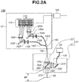
- Fig. 2A is a detailed partial view illustrating a spectral information acquisition unit 100 of the identification apparatus 1000 illustrated in Fig. 1 .
- Fig. 2B is a diagram illustrating a projection of optical spectra 280sl and 280sh to an imaging unit 170.
- Fig. 2C is a diagram illustrating a relationship between light detection element numbers in a row direction 172r of the imaging unit 170 and wavenumbers of optical spectra projected in the row direction 172r.
- the light detection element numbers are also referred to as "row direction addresses of light detection elements" or "row direction numbers of light detection elements”.
- a z-direction corresponds to a vertical direction and a gravity direction
- an x-direction corresponds to a conveyance direction dc
- a y-direction corresponds to a conveyance width direction dw
- an xy-plane corresponds to a horizontal surface.
- the conveyance width direction dw is parallel to a conveyance surface 200S and corresponds to a direction orthogonal to the conveyance direction dc.
- the identification apparatus 1000 includes an irradiation unit 22 as illustrated in Fig. 1 .
- the irradiation unit 22 irradiates a sample 900i conveyed in the conveyance direction dc with irradiation light 220 to focus the irradiation light 220 on the sample 900i.
- the sample 900i is fed to a conveyance unit 200 by a feeder 500 and conveyed along the conveyance direction dc by the conveyance unit 200.
- the irradiation light 220 is also referred to as converged light 220 or primary light 220.
- the identification apparatus 1000 includes a light collecting unit 20 corresponding to the irradiation unit 22 as illustrated in Fig. 1 .
- the light collecting unit 20 collects scattered light from the sample 900i.
- the identification apparatus 1000 also includes an acquisition unit 30 as illustrated in Fig. 1A.
- the acquisition unit 30 acquires identification information for identifying properties of the sample 900i based on the light collected by the light collecting unit 20.
- the identification apparatus 1000 also includes the conveyance unit 200 and a discrimination apparatus 300 situated downstream of the conveyance unit 200 in the conveyance direction dc, as illustrated in Fig. 1 .
- the conveyance unit 200 includes a conveyer belt that conveys the sample 900i at a conveyance velocity vc in the x-direction.
- a spectral information acquisition unit included in the identification apparatus 1000 and having a spectroscopic element and an imaging unit according to a feature of the present invention will now be described in detail with reference to Fig. 2A .
- the identification apparatus 1000 includes the spectral information acquisition unit 100 configured to acquire spectral information about light collected from the sample 900i.
- the spectral information acquisition unit 100 is a unit that acquires a Raman shift from a difference in wavenumber between Raman scattered light contained in secondary light from the sample 900i and excitation light contained in primary light.
- the spectral information acquisition unit 100 includes the irradiation unit 22 and the light collecting unit 20 as illustrated in Figs. 1 and 2A .
- the irradiation unit 22 irradiates the sample 900i with the irradiation light 220, and the light collecting unit 20 collects the secondary light from the sample 900i.
- the irradiation unit 22 and the light collecting unit 20 according to the present exemplary embodiment are situated on the same axis, and the irradiation unit 22 is optically coupled to a light source 25 including a laser light source via an optical fiber 130.
- the light collecting unit 20 is optically coupled to a spectral image acquisition unit 10 to enable the spectral information acquisition unit 100 to acquire optical information reflecting a material contained in the sample 900i.
- Fig. 2A is a diagram schematically illustrating an example of a configuration of the spectral information acquisition unit 100.
- the spectral information acquisition unit 100 includes a light collecting unit 27 having the irradiation unit 22 and the light collecting unit 20.
- the irradiation unit 22 irradiates the sample 900i with light, and the light collecting unit 20 collects Raman scattered light from the sample 900i.
- the irradiation unit 22 and the light collecting unit 20 are situated on the same axis on the sample side (object side) when viewed from a dichroic mirror 250, and a positional deviation is less likely to occur between a center of an irradiation spot and a center of scattered light to be collected even in a case where an irradiated surface of the sample 900i has a difference in height or is tilted.
- the irradiation unit 22 is situated above the conveyance unit 200 and has a focal distance DF to form a focal plane 65 at a position at a predetermined distance from the conveyance surface 200S of the conveyer belt.
- the irradiation unit 22 is situated to focus the irradiation light 220 on an upper side of the sample 900i to increase the scattering intensity of Raman scattered light, which is weaker by several orders of magnitude than Rayleigh scattered light.
- a unit including the irradiation unit 22 and the light source 25 is also referred to as an irradiation optical system.
- the irradiation unit 22 includes an objective lens 260, the dichroic mirror 250, a collimator lens 230, a cylindrical lens 240, and a reflection mirror 210 as illustrated in Fig. 2A .
- the objective lens 260 employs a convex lens, a collimator lens, a concave lens, and/or a zoom lens.
- Synthetic quartz can be used as a glass material for the collimator lens 230, the cylindrical lens 240, and the objective lens 260.
- the collimator lens 230, the cylindrical lens 240, and the objective lens 260 are irradiated with high-output light from a semiconductor laser 25, but use of synthetic quartz as a material for these glass lenses can reduce background components of fluorescence and Raman scattered light.
- the objective lens 260 acts as a condenser lens that condenses light from the laser light source 25 to the sample 900i in the irradiation unit 22.
- the objective lens 260 forms the focal plane 65 at a focal distance DF from the objective lens 260, a focal point (focal spot) with a focal diameter ⁇ (not illustrated), and a focal depth ⁇ DF correspondingly to a numerical aperture NA.
- the collimator lens 230 and the cylindrical lens 240 reduce the spread of emitted light from the laser light source 25 and shape the light into parallel light.
- the cylindrical lens 240 can use another optical element for collimating such as an anamorphic prism pairs.
- a wavelength filter such as a laser line filter can be provided at the position of a pupil surface of the irradiation unit 22. This improves wavelength characteristics of light with which the sample 900i is irradiated by the irradiation unit 22.
- the irradiation unit 22 can be shared with the light collecting unit 20. Since the light collecting unit 20 and the irradiation unit 22 according to the present exemplary embodiment are situated on the same axis, the objective lens 260 and the dichroic mirror 250 are shared by the light collecting unit 20 and the irradiation unit 22.
- the light source 25 is a light source that emits excitation light to the irradiation unit 22 via the optical fiber 130.
- the irradiation optical system that disperses Raman scattered light uses a laser light source with a wavelength of 400 nm to 1100 nm as the light source 25. In Raman scattering, the excitation efficiency increases at shorter wavelengths, and fluorescence components to be a background decrease at longer wavelengths.
- a wavelength selected as an excitation wavelength of a laser light source applied to the light source 25 is desirably a wavelength from which a difference in Raman shift between a target material and a non-target material is distinctively obtained, and there is a case where at least one of 532 nm, 633 nm, 780 nm, and 1064 nm is used. While use of the semiconductor laser 25 as a light source of the irradiation unit 22 is described herein, the light source is not limited to that described herein, and another laser light source such as a semiconductor excited solid-state laser or a gas laser can be used.
- the light collecting unit 20 is situated above the conveyance surface 200S to collect the secondary light emitted from a top surface of the sample 900i conveyed by the conveyance unit 200.
- the light collecting unit 20 is situated above the conveyance unit 200 corresponding to an irradiation region of the irradiation light 220 emitted from the irradiation unit 22 to collect the secondary light from the top surface of the sample 900i conveyed through the irradiation region.
- the light collecting unit 20 includes the objective lens 260, the dichroic mirror 250, an imaging lens 270, and an optical fiber 190.
- the objective lens 260 of the light collecting unit 20 includes a convex lens, a collimator lens, a concave lens, and/or a zoom lens as those included in the irradiation unit 22.
- the light collecting unit 20 may include a wavelength filter, such as a band-pass filter or a long-pass filter to reduce excitation light components contained in the primary light, in order to reduce unnecessary light in spectroscopic measurement.
- the light collecting unit 20 employs an objective lens having a large numerical aperture to ensure light collection efficiency.
- An objective lens with a numerical aperture of 0.1 or more to 0.5 or less is employed as the objective lens 260 of the light collecting unit 20. More specifically, an objective lens B-270 manufactured by SCHOTT having an effective lens diameter of 25 mm, a focal distance of 20 mm, and a numerical aperture of 0.5 can be used as the objective lens 260.
- the spectral image acquisition unit 10 includes a branch portion 195, imaging lenses 1101 and 110h, band-pass filters 1201 and 120h, spectroscopic elements 1501 and 150h, and the imaging unit 170 in this order from the light collecting unit 20 side as illustrated in Fig. 2A .
- the letters 1 (the lowercase letter of "L" of the alphabet) and h are added at the end of each reference numeral to indicate the low-wavenumber side and the high-wavenumber side, respectively.
- the spectroscopic elements 1501 and 150h are situated to disperse light collected by the light collecting unit 20 through imaging lenses 1601 and 160h and to project a continuous spectrum to the imaging unit 170 along a row or column direction of a light detection element array of the imaging unit 170.
- the optical spectrum 280sl of low wavenumbers and the optical spectrum 280sh of high wavenumbers are projected to the imaging unit 170 along light detection elements 350 arrayed in the row direction 172r, according to the present exemplary embodiment as illustrated in Figs. 2A and 2B .
- the optical spectrum 280sl of low wavenumbers and the optical spectrum 280sh of high wavenumbers are projected to the imaging unit 170 along the row direction 172r discontinuously with a non-projection band NPB between row-direction element numbers 1041 and 1042 as illustrated in Fig. 2C .
- the non-projection band NPB is set correspondingly to a silent region of 1800 cm -1 to 2800 cm -1 .
- the non-projection band NPB is also referred to as "non-projection band" or "non-projection wavenumber range”.
- the non-projection band NPB is desirably set to a wavenumber range of 200 cm -1 or higher, more desirably a wavenumber range of 500 cm -1 or higher.
- an optical spectrum of high wavenumbers from 1800 cm -1 to 4000 cm -1 and an optical spectrum of low wavenumbers from 500 cm -1 to 1800 cm -1 in the 3500-cm -1 wavenumber range of received light from 500 cm -1 to 4000 cm -1 excluding the non-projection band NPB of 1000 cm -1 are projected to the imaging unit 170.
- a wavenumber width that can be divided by a single light detection element according to the present exemplary embodiment is reduced to 745/1040 at the low wavenumbers and 645/960 at the high wavenumbers compared to projections illustrated in Figs. 5A and 5B according to a conventional technique, and the spectral resolution in the wavenumber direction is improved.
- the optical spectrum of the low wavenumbers ranging from 500 cm -1 to 1800 cm -1 and the optical spectrum of the high wavenumbers ranging from 1800 cm -1 to 4000 cm -1 are projected discontinuously from each other by arranging the spectroscopic element 1501 for the low wavenumbers and the spectroscopic element 150h for the high wavenumbers are shifted in the row direction 172r of the imaging unit 170.
- the spectroscopic element 1501 for low wavenumbers and the spectroscopic element 150h for high wavenumbers respectively project the plurality of optical spectra 280sl and 280sh having a different wavenumber range from each other to a plurality of regions of the imaging unit 170.
- the plurality of optical spectra 280sl and 280sh having a different wavenumber range from each other is projected to a plurality of regions of the imaging unit 170 with the non-projection band NPB, which is not projected to the imaging unit 170, between the optical spectra 280sl and 280sh.
- exit ends of optical fibers 1901 and 190h are arranged in parallel and shifted vertically on the sheet plane of Fig. 2A with respect to one of the spectroscopic elements 1501 and 150h.
- optical spectra of low and high wavelengths are discontinuously projected to the imaging unit 170 along the row direction 172r from the one of the spectroscopic elements 1501 and 150h.
- the other one of the spectroscopic elements 1501 and 150h, the corresponding imaging lens 1101 or 110h, the other one of the band-pass filters 1201 and 120h, and the branch portion 195 can be omitted.
- the spectroscopic elements 1501 and 150h do not have to be the same spectroscopic element, and each can be optimized as needed based on a lattice period and a wavenumber band of a central wavelength to be projected in order to project spectral images of low and high wavelengths to a wide region on the imaging unit 170.
- the imaging unit 170 is situated at an optimum position in line with an individual emission angle of the spectroscopic elements 1501 and 150h considering diffraction efficiency and wavenumber resolution.
- the imaging unit 170 employs an imaging device, such as a charge-coupled device (CCD) image sensor or a complementary metal oxide semiconductor (CMOS) image sensor, with light detection elements arranged two-dimensionally.
- the plurality of light detection elements 350 of the imaging unit 170 according to the present exemplary embodiment is arranged in a matrix. In a case where the plurality of light detection elements 350 is arranged in a delta array, however, row and column directions are associated with two of three axes or are associated with a direction of one of the three axes and a combined direction of a combination of the remaining two axes.
- the identification apparatus 1000 identifies properties of the sample 900i while the conveyance unit 200 conveys the sample 900i, and the discrimination apparatus 300 discriminates the sample 900i based on the identification result. Thus, it is desirable to increase the conveyance velocity vc of the conveyance unit 200 in order to increase the throughput of the sorting processing by the identification apparatus 1000.
- the optical spectra 280sl and 280sh projected onto the imaging unit 170 are based on Raman scattered light generated from the sample 900i moving on the conveyance surface 200S.
- the optical spectra 280sl and 280sh are projected onto the imaging unit 170 while the conveyed sample 900i is in the irradiation region of the irradiation light 220 (the converged light 220) emitted from the irradiation unit 22.
- the conveyance velocity vc of the conveyance unit 200 is 2 m/second and the length of the sample 900i in the conveyance direction dc is 10 mm
- the time during which the imaging unit 170 can detect a spectral image formed by Raman scattered light from the sample 900i is 5 milliseconds or less.
- the imaging unit 170 is therefore required to have a high frame rate.
- An imaging unit with a high frame rate is a CMOS image sensor, and therefore the imaging unit 170 is desirably a CMOS image sensor.
- the intensity of Raman scattered light from the sample 900i is significantly low, so that the intensity of incident light on each element of the light detection elements 350 of the imaging unit 170 is also significantly low. It is therefore desirable to use an imaging unit with high sensitivity to the wavenumber region where spectral images corresponding to the optical spectra 280sl and 280sh are acquired, as the imaging unit 170.
- a rolling shutter image sensor has a simpler pixel structure and a higher aperture ratio than a global shutter image sensor, and photoelectric conversion elements can be enlarged, so that the sensitivity and the dynamic range can be increased.
- a rolling shutter image sensor has an advantage that the cost is lower than a global shutter image sensor. For the foregoing reasons, a rolling shutter CMOS image sensor is used as the imaging unit 170 according to the present exemplary embodiment.
- the imaging unit 170 can employ a rolling reset type image sensor that sequentially resets each row of the array of the light detection elements 350. This increases the exposure time of each row of the array of the light detection elements 350 as long as possible, and the sensitivity increases.
- the imaging unit 170 includes a crop reading function of reading a specific row in a light receiving unit 171 including the light detection elements 350 arrayed two-dimensionally in the row direction 172r and a column direction 172c.
- a morphologic information acquisition unit 70 described below detects an arrival of the sample 900i at a light collectable region of the light collecting unit 20
- the imaging unit 170 reads a specific row in the light receiving unit 171 corresponding to the light collecting unit 20.
- the imaging unit 170 includes a reading circuit 173, a horizontal scan circuit 174, a vertical scan circuit 175, and an output circuit 176.
- the imaging unit 170 sequentially reads signals from a plurality of pixels arranged in a matrix shape row by row.
- the vertical scan circuit 175 selects a row in the light receiving unit 171 and drives the selected row.
- the reading circuit 173 reads signals output from the pixels of the row selected by the vertical scan circuit 175 and transfers the read signals to the output circuit 176 based on control by the horizontal scan circuit 174. This is how the reading in a main-scan direction (row direction) is performed.
- the row selected by the vertical scan circuit 175 is shifted, and the reading circuit 173 performs reading in the main-scan direction based on control by the horizontal scan circuit 174.
- the foregoing operations are repeated so that the selected row is shifted in a sub-scan direction (column direction), and thereby signals from the entire light receiving unit 171 are read.
- the read signals are output as output signals to a material information reference unit 180 through an output terminal 177 of the output circuit 176.
- the material information reference unit 180 is situated outside the imaging unit 170. At this time, the scanning in the main-scan direction is performed at high speed, and the scanning in the sub-scan direction is slower than the scanning in the main-scan direction.
- the imaging lenses 1101 and 110h changes, into parallel light, branch light transmitted through the optical fiber 190 from the light collecting unit 20 and through one of the optical fibers 1901 and 190h from the branch portion 195.
- the optical fibers 1901 and 190h are also referred to as branch light guide portions 1901 and 190h.
- the band-pass filters 1201 and 120h reduce the intensity of excitation light components contained in the collected light and transmit a portion of Raman scattered light components.
- the band-pass filters 1201 and 120h have spectral transmission characteristics to attenuate Raman scattered light of high wavenumbers and Raman scattered light of low wavenumbers, respectively.
- the spectroscopic elements 1501 and 150h disperse collected light to spread wavelength components in a fan-shaped form.
- the imaging lenses 1601 and 160h project the light dispersed by the spectroscopic elements 1501 and 150h onto the imaging unit 170.
- the spectroscopic elements 1501 and 150h are transmissive diffractive gratings. Reflective diffractive gratings can also be used as the diffractive gratings. In this case, a spectroscopic element configuration employs a Rowland arrangement or a Czerny-Turner configuration.
- the spectroscopic elements 1501 and 150h are also referred to as diffractive gratings 1501 and 150h.
- the imaging unit 170 acquires spectral information Si about the sample 900i considering a captured spectral image, photoelectric conversion characteristics of an image sensor of the imaging unit 170, and transmission characteristics of an optical system.
- the spectroscopic elements 1501 and 150h can also acquire polarization information including circular dichroism and optical rotatory dispersion together with optical spectra.
- the spectral information acquisition unit 100 includes the material information reference unit 180, which acquires material information about the sample 900i based on the spectral information Si acquired by the spectral image acquisition unit 10.
- the material information reference unit 180 refers to a material database (not illustrated) storing Raman scattered light reference data and acquires material information Mi based on the similarity between the spectral information Si and reference data.
- the material information Mi identifies materials contained in the sample 900i.
- the spectral information acquisition unit 100 stores at least one of the spectral information Si and the material information Mi in a first storage unit 60 via an instruction unit 40 described below.
- the material database that the material information reference unit 180 refers to can be stored on a local server of the identification apparatus 1000 or on a remote server that is accessible via the Internet or an intranet.
- the spectral information acquisition unit 100 acquires the material information Mi about mixtures of, for example, materials, additives, and impurity components contained in the sample 900i.
- the morphologic information acquisition unit 70 includes a camera 76 and an image processing unit 78, as illustrated in Fig. 1 , and acquires morphologic information Fi about the sample 900i.
- the camera 76 is situated such that an imaging field of view 700 overlaps the conveyance unit 200.
- the image processing unit 78 processes an image of a sample captured by the camera 76.
- the morphologic information Fi is information about properties of the sample 900i.
- the image processing unit 78 performs image processing including contrast and contour extraction, and acquires, for example, the length of each sample 900i in the conveyance direction dc, and the reflected color of each sample 900i, the shape of each sample 900i, and the mixing level of materials of each sample 900i.
- the image processing unit 78 is also referred to as an element that performs processing to acquire size information about each sample 900i.
- the morphologic information acquisition unit 70 can include a photo-interrupter (not illustrated) and a laser interferometer (not illustrated) in place of the camera 76.
- the morphologic information acquisition unit 70 is also referred to as an imaging unit.
- the morphologic information acquisition unit 70 is also an element selectively employed in the identification apparatus 1000.
- the acquisition unit 30 acquires identification information Di about whether the sample 900i is a target sample or a non-target sample based on the material information Mi or the spectral information Si acquired by the spectral information acquisition unit 100 and the morphologic information Fi acquired by the morphologic information acquisition unit 70 as illustrated in Fig. 1 .
- the acquisition unit 30 acquires the identification information Di for each sample 900i.
- the acquisition unit 30 outputs the acquired identification information Di to the instruction unit 40.
- the acquisition unit 30 identifies properties of the sample 900i based on a Raman spectrum contained in the secondary light of the light collected by the light collecting unit 20.
- the acquisition unit 30 according to the present exemplary embodiment identifies properties of each sample 900i based on the image of the sample acquired from the camera 76 and the Raman spectrum contained in the secondary light of the light collected by the light collecting unit 20.
- the spectral information acquisition unit 100 and the morphologic information acquisition unit 70 according to the present exemplary embodiment can be replaced with a hyperspectral camera or a multiband camera capable of acquiring the morphologic information Fi and the spectral information Si from a captured image, according to a modified form.
- an identification apparatus (not illustrated) according to the modified form includes a detection system that acquires multi-dimensional data from which material information and morphologic information are readable.
- the identification apparatus 1000 includes a control unit 400 including the instruction unit 40, a second storage unit 80, and the first storage unit 60.
- the instruction unit 40 controls the discrimination operation of the discrimination apparatus 300 based on the properties of each sample 900i.
- the second storage unit 80 stores a control condition of the discrimination operation.
- the first storage unit 60 stores the properties of each sample 900i.
- the control unit 400 includes a display unit 140 configured to provide a graphical user interface (GUI) via which a user can designate the control condition.
- GUI graphical user interface
- the first storage unit 60 is configured to store, for each sample 900i, the identification information Di, the material information Mi, the spectral information Si, and the morphologic information Fi in association with a timing tp of the passing of the sample 900i through the irradiation light 220.
- the second storage unit 80 is configured to store a control condition for controlling an intensity Is of the discrimination operation of the discrimination apparatus 300 that corresponds to the identification information Di for each sample 900i.
- Forms of the control condition include a table for reference, an algebraically-expressed general formula, and machine-learned statistical information.
- the instruction unit 40 estimates the time of the passing of the sample 900i through a processing region where the discrimination apparatus 300 performs discrimination processing on the sample 900i based on the materials and size of each sample 900i based on the identification information Di from the acquisition unit 30, and generates an instruction to control the discrimination operation of the discrimination apparatus 300.
- the time of the passing of the sample 900i through the processing region can be estimated based on at least one of a signal from the morphologic information acquisition unit 70, a signal from the spectral information acquisition unit 100, and a signal from a sample sensor (not illustrated) of the conveyance unit 200.
- the discrimination apparatus 300 includes an air nozzle 330 and a discrimination control unit 340 as illustrated in Fig. 1 .
- the air nozzle 330 discharges compressed air for a predetermined discharge time, at a predetermined discharge velocity, and at a predetermined discharge flow rate.
- the discrimination control unit 340 controls a solenoid valve (not illustrated) of the air nozzle 330.
- the discrimination control unit 340 receives a control signal from the instruction unit 40 of the identification apparatus 1000.
- the discrimination operation of the discrimination apparatus 300 includes an operation of discharging a fluid.
- the fluid to be discharged by the discharge operation includes air, dry nitrogen, inert gas such as a noble gas, liquid, and gas-liquid mixture fluid (aerosol).
- the discrimination apparatus 300 collects the sample 900i into a target collection basket 620 and a non-target collection basket 600 or 640 according to the properties of the sample 900i based on the control signal from the instruction unit 40.
- a discharge apparatus of the discrimination apparatus 300 that discharges a fluid can be replaced with a flap gate that opens and closes at a predetermined angular velocity or a shutter that opens and closes at a predetermined velocity.
- the morphologic information acquisition unit 70, the spectral information acquisition unit 100, the discrimination apparatus 300, and components thereof included in the identification apparatus 1000 are situated in parallel at different positions in the conveyance width direction dw of the conveyance unit 200 for system consolidation and high-speed processing.
- the discrimination apparatus 300 can be considered as an element of the identification apparatus 1000 and is sometimes referred to as a discrimination unit 300.
- the conveyance unit 200 and the feeder 500 form a conveyance unit that conveys the sample 900i.
- the conveyance unit 200 includes the conveyer belt that conveys the sample 900i fed from the feeder 500 in the conveyance direction dc at the velocity vc linearly on the conveyance surface 200S.
- the conveyance unit 200 can be replaced with a turntable feeder that externally conveys a sample spirally, a vibrating feeder equipped with a vibration generator that moves a sample in a predetermined direction, or a conveyer roller including a plurality of rollers, according to a modified example.
- the conveyance unit 200 moves the sample 900i such that the sample 900i passes through the imaging field of view 700 of the camera 76.
- the conveyance unit 200 is also referred to as a placement portion 200 with respect to the morphologic information acquisition unit 70.
- the conveyance unit 200 moves the sample 900i such that the sample 900i passes through an effective light collection region (not illustrated) of the light collecting unit 20.
- the conveyance unit 200 is also referred to as the placement portion 200 with respect to the light collecting unit 20.
- the conveyance velocity vc of the conveyance unit 200 that is 0.1 m/s to 5 m/s is applicable in a case of the conveyer belt.
- a case where the classifying processing for filtering the shape and size of the sample 900i is performed as the preprocessing of the feeding by the feeder 500 is also a modified form of the identification method using the identification apparatus 1000 according to the present exemplary embodiment.
- a vibrating conveyer, a vibrating sieving machine, or a crushed grain checking machine is used as a unit that performs preprocessing.
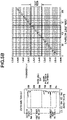
- Fig. 3B is a diagram illustrating a relationship between the light detection element numbers of light detection elements arrayed in the row direction 172r of the imaging unit 170 according to the present exemplary embodiment and the wavenumbers of optical spectra projected in the row direction 172r.
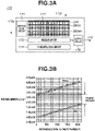
- the identification apparatus is different from the identification apparatus 1000 according to the first exemplary embodiment in that the optical spectra 280sl and 280sh are projected to different positions on the imaging unit 170 in the row direction 172r and the column direction 172c as illustrated in Fig. 3A .
- the present exemplary embodiment and the first exemplary embodiment are different in the directions of discontinuous projections of the optical spectra 280sl and 280sh to the imaging unit 170.
- the identification apparatus is similar to the first exemplary embodiment in that the spectral image acquisition unit 10 includes two sets of spectroscopic elements 1501 and 150h with respect to one imaging unit 170, whereas the present exemplary embodiment is different from the first exemplary embodiment in the arrangement of the spectroscopic elements 1501 and 150h with respect to the imaging unit 170.
- the spectroscopic elements 1501 and 150h are shifted in the row direction 172r.
- the spectroscopic elements 1501 and 150h are shifted in the column direction 172c (not illustrated).
- the optical spectrum 280sl of low wavenumbers and the optical spectrum 280sh of high wavenumbers are projected to the light receiving unit 171 of the imaging unit 170 along the light detection elements 350 arrayed in the row direction 172r as illustrated in Fig. 3A .
- the optical spectrum 280sl of low wavenumbers and the optical spectrum 280sh of high wavenumbers are projected to the imaging unit 170 with the non-projection band NPB between the optical spectra 280sl and 280sh in the column direction 172c as illustrated in Fig. 3B .
- the optical spectrum 280sl of low wavenumbers and the optical spectrum 280sh of high wavenumbers are projected correspondingly to the light detection elements 350 corresponding to element numbers 101 to 2101 along the row direction 172r.
- the non-projection band NPB is set correspondingly to the silent region of 1800 cm -1 to 2800 cm -1 as described in the first exemplary embodiment.
- the optical spectra 280sl and 280sh of the low-wavenumber band of 500 cm -1 to 1800 cm -1 and the high-wavenumber band of 1800 cm -1 to 4000 cm -1 excluding the non-projection band NPB of 1000 cm -1 are shifted in the column direction 172c and projected to the imaging unit 170.
- a wavenumber width that can be divided by a single light detection element according to the present exemplary embodiment is reduced to 745/2000 at the low wavenumbers and 645/2000 at the high wavenumbers compared to projections illustrated in Figs. 5A and 5B according to a conventional technique, and the spectral resolution in the wavenumber direction is improved.
- Fig. 4A corresponds to a diagram illustrating a projection of a light collecting optical system and a discrimination apparatus of an identification apparatus 2000 to a plane A-A' illustrated in Fig. 1 as a projection plane.
- a cross section B-B' in Fig. 4A corresponds to the schematic configuration diagram illustrated in Fig. 1 .
- the identification apparatus 2000 illustrated in Fig. 4A is different from the identification apparatus 1000 illustrated in Fig. 1 in that four imaging fields 700-p of the camera 76, four irradiation spots from the irradiation unit 22-p, and four air nozzles 330-p of the discrimination apparatus 300 are arranged in the conveyance width direction dw.
- the identification apparatus 2000 is a multi-column identification apparatus including a plurality of units for identification arranged in parallel at different positions in the conveyance width direction dw intersecting with the conveyance direction dc.
- the identification apparatus 2000 realizes system consolidation and high-speed identification processing compared to those of the identification apparatus 1000.
- the identification apparatus 2000 includes the imaging fields 700-p, irradiation spots 220-p of the primary light, and air nozzles 300-p arranged in series correspondingly to the respective tracks TRp.
- the identification apparatus 2000 includes a feeder 500A and a multi-discrimination apparatus (not illustrated). An air supply port of the feeder 500A is arrayed.
- the air nozzles 300-p of the multi-discrimination apparatus are a multi-nozzle.
- the light collecting optical system includes four low-wavenumber band-pass filters, four high-wavenumber band-pass filters, four low-wavenumber imaging lenses, four high-wavenumber imaging lenses, four low-wavenumber optical fibers, and four high-wavenumber optical fibers correspondingly to the number of rows p, which is four.
- Respective exit ends of the plurality of low-wavenumber optical fibers and the high-wavenumber optical fibers according to the present exemplary embodiment are arrayed at predetermined intervals in one line in the vertical direction of Fig. 2A to form a one-dimensional exit end array.
- the spectroscopic elements 1501-p and 150h-p are shifted along the row direction 172r and projected in the imaging unit 170 as described in the first exemplary embodiment.
- the low-wavenumber band of 500 cm -1 to 1800 cm -1 and the high-wavenumber band of 2800 cm -1 to 4000 cm -1 that are respectively projected from the spectroscopic elements 1501-p and 150h-p are discontinuously projected to the imaging unit 170 with the non-projection band NPB therebetween as described in the first exemplary embodiment.
- a wavenumber width that can be divided by a single light detection element according to the present exemplary embodiment is therefore reduced to 745/1040 at the low wavenumbers and 645/960 at the high wavenumbers compared to the conventional technique illustrated in Figs. 5A and 5B , similarly to the first exemplary embodiment.
- the spectral resolution of optical spectra 280sl1 to 280sl4 of low wavenumbers and optical spectra 280sh1 to 280sh4 of high wavenumbers in the wavenumber direction is improved compared to the conventional technique illustrated in Figs. 5A and 5B , similarly to the first exemplary embodiment.
- one of the exit end arrays according to the present exemplary embodiment can be juxtaposed with one spectroscopic element in the vertical direction of Fig. 2A as described in the first exemplary embodiment.
- one spectroscopic element can discontinuously project the optical spectra 280slp and 280shp in the row direction 172r.
- the exit ends can be arranged in the vertical direction of Fig. 2A to form a two-dimensional array.
- optical spectrum refers to an intensity distribution of diffraction light projected in the fan-shaped form from the spectroscopic element for each wavenumber
- optical spectrum may be used to also refer to a spatial spread of diffraction light and a spectral image captured by the imaging unit.
- the present invention provides an identification apparatus including a spectroscopic element situated to effectively disperse collected light and an imaging unit.
- the present invention provides an identification apparatus that ensures a spectral resolution of a wavenumber band useful in identifying properties of a sample.
Landscapes
- Physics & Mathematics (AREA)
- Spectroscopy & Molecular Physics (AREA)
- General Physics & Mathematics (AREA)
- Health & Medical Sciences (AREA)
- Life Sciences & Earth Sciences (AREA)
- Chemical & Material Sciences (AREA)
- Analytical Chemistry (AREA)
- Biochemistry (AREA)
- General Health & Medical Sciences (AREA)
- Immunology (AREA)
- Pathology (AREA)
- Nuclear Medicine, Radiotherapy & Molecular Imaging (AREA)
- Investigating, Analyzing Materials By Fluorescence Or Luminescence (AREA)
Abstract
Description
- The present invention relates to an identification apparatus that identifies properties such as a composition and constituents of a sample based on scattered light from the sample.
- An identification apparatus that optically identifies properties of a sample using spectroscopic analysis is known. Such an identification apparatus is installed in a conveyance path for conveying a plurality of samples and is used to inspect products and to sort wastes.
- Spectroscopic analysis does not always require processes, such as vacuum decompression, atmosphere control, immersion in liquid, and atmosphere management for drying that limit the throughput, and properties of a sample can be identified under an atmospheric atmosphere. Thus, attempts to apply the spectroscopic analysis to the sorting of waste resins have been made in recent years.
- Known types of spectroscopic analysis are infrared absorption spectroscopy and Raman scattering spectroscopy. Infrared absorption spectroscopy acquires an absorption spectrum of a sample with respect to incident light containing an infrared wavelength band. Raman scattering spectroscopy acquires a scattering spectrum of a sample with respect to incident light containing an ultraviolet wavelength band. Raman scattering spectroscopy is less likely to be affected by light attenuation due to the thickness of the sample and is therefore used in identifying wastes of different sample sizes. A Raman scattering spectroscopic method of dispersing Raman scattered light uses Raman shifts specific to atomic bonds constituting a hydrocarbon and is therefore suitable for use in identifying a resin.
- The intensity of Raman scattered light is lower by several orders of magnitude than elastic scattered components (Rayleigh scattered light) contained in secondary light, so that a method of converging primary light and irradiating a sample with the converged light is employed to increase the detection sensitivity per unit area. There is a known sorting apparatus that sorts samples into a target sample and others based on whether a predetermined target condition is satisfied based on a detected spectrum.
- BUNSEKI-KAGAKU Vol. 61, No. 12, pp. 1027-1032 (2012) discusses a waste resin identification apparatus including a light collecting unit, a spectroscopic element, and a charge-coupled device (CCD) image sensor having 1024-by-64 (row direction by column direction) elements arrayed in a two-dimensional matrix. The identification apparatus discussed in BUNSEKI-KAGAKU Vol. 61, No. 12, pp. 1027-1032 (2012) projects an optical spectrum from the spectroscopic element along a lengthwise direction (row direction) of the CCD image sensor. BUNSEKI-KAGAKU Vol. 61, No. 12, pp. 1027-1032 (2012) further discusses acquisition of a spectral image at high speed by reading an optical spectrum projected from the spectroscopic element in the column direction.
Japanese Patent Application Laid-Open No. 2019-105628 Japanese Patent Application Laid-Open No. 2019-105628 Japanese Patent Application Laid-Open No. 2019-105628 - The identification apparatuses discussed in BUNSEKI-KAGAKU Vol. 61, No. 12, pp. 1027-1032 (2012) and
Japanese Patent Application Laid-Open No. 2019-105628 - Meanwhile, a Raman scattering spectrum has a Raman shift peak wavenumber corresponding to a specific functional group in the wavenumber range of 4000 cm-1 to 100 cm-1.
Fig. 5A illustrates a Raman scattering spectrum of polystyrene as an example of a hydrocarbon contained in a waste resin. Characteristics peak shifts in the wavenumber range of 4000 cm-1 to 100 cm-1 are not uniform but uneven, and the wavenumber range is divided in the wavenumber direction. It is known to divide the Raman spectroscopy wavenumber range into three regions i.e., a fingerprint region (500 cm-1 to 1800 cm-1), a silent region, and a C-H stretch region (2800 cm-1 to 3100 cm-1) from low wavenumbers toward high wavenumbers. Useful peak shifts appear less frequently in the silent region (1800 cm-1 to 2800 cm-1) between the fingerprint region and the C-H stretch region than in the fingerprint region and the C-H stretch region on spectral identification. - Thus, the number of light detection elements corresponding to the silent region of the optical spectrum projected to the imaging units of the identification apparatuses discussed in BUNSEKI-KAGAKU Vol. 61, No. 12, pp. 1027-1032 (2012) and
Japanese Patent Application Laid-Open No. 2019-105628 Fig. 5B . In other words, the number of light detection elements corresponding to the silent region is 1/4 to 2/5 the number of light detection elements corresponding to the entire region of the spectrum projected in the row direction, and therefore the spectral identification capacity is decreased by 3/4 to 3/5. - The present invention is directed to an identification apparatus including a spectroscopic element situated to effectively disperse collected light and an imaging unit. Specifically, the present invention is directed to an identification apparatus that ensures a spectral resolution of a wavenumber band useful in identifying properties of a sample.
- According to an aspect of the present invention, there is provided an identification apparatus as specified in
claims 1 to 15. - Further features of the present invention will become apparent from the following description of exemplary embodiments with reference to the attached drawings.
-
-
Fig. 1 is a diagram illustrating a schematic configuration of an identification apparatus according to a first exemplary embodiment. -
Fig. 2A is a block diagram illustrating a schematic configuration of a spectral information acquisition unit.Figs. 2B and 2C illustrate a projection of an optical spectrum to an imaging device according to the first exemplary embodiment. -
Figs. 3A and 3B are diagrams illustrating a projection of an optical spectrum to an imaging device according to a second exemplary embodiment. -
Fig. 4A is a diagram illustrating a schematic configuration of an identification apparatus.Fig. 4B illustrates a projection of an optical spectrum to an imaging device according to a third exemplary embodiment. -
Fig. 5A is a diagram illustrating a Raman scattering spectrum of polystyrene.Fig. 5B illustrates a projection of an optical spectrum to an imaging device according to a conventional technique. - Various exemplary embodiments of the present invention will now be described with reference to the drawings. Each of the embodiments of the present invention described below can be implemented solely or as a combination of a plurality of the embodiments or features thereof where necessary or where the combination of elements or features from individual embodiments in a single embodiment is beneficial.
- An identification apparatus according to a first exemplary embodiment will now be described with reference to
Figs. 1 ,2A ,2B, and 2C .Fig. 1 is a diagram schematically illustrating a configuration of anidentification apparatus 1000 according to the present exemplary embodiment.Fig. 2A is a detailed partial view illustrating a spectralinformation acquisition unit 100 of theidentification apparatus 1000 illustrated inFig. 1 .Fig. 2B is a diagram illustrating a projection of optical spectra 280sl and 280sh to animaging unit 170.Fig. 2C is a diagram illustrating a relationship between light detection element numbers in arow direction 172r of theimaging unit 170 and wavenumbers of optical spectra projected in therow direction 172r. The light detection element numbers are also referred to as "row direction addresses of light detection elements" or "row direction numbers of light detection elements". - In
Fig. 1 , a z-direction corresponds to a vertical direction and a gravity direction, an x-direction corresponds to a conveyance direction dc, a y-direction corresponds to a conveyance width direction dw, and an xy-plane corresponds to a horizontal surface. The conveyance width direction dw is parallel to aconveyance surface 200S and corresponds to a direction orthogonal to the conveyance direction dc. - The
identification apparatus 1000 includes anirradiation unit 22 as illustrated inFig. 1 . Theirradiation unit 22 irradiates asample 900i conveyed in the conveyance direction dc with irradiation light 220 to focus theirradiation light 220 on thesample 900i. Thesample 900i is fed to aconveyance unit 200 by afeeder 500 and conveyed along the conveyance direction dc by theconveyance unit 200. Theirradiation light 220 is also referred to as converged light 220 orprimary light 220. - The
identification apparatus 1000 includes alight collecting unit 20 corresponding to theirradiation unit 22 as illustrated inFig. 1 . Thelight collecting unit 20 collects scattered light from thesample 900i. Theidentification apparatus 1000 also includes anacquisition unit 30 as illustrated in Fig. 1A. Theacquisition unit 30 acquires identification information for identifying properties of thesample 900i based on the light collected by thelight collecting unit 20. - The
identification apparatus 1000 also includes theconveyance unit 200 and adiscrimination apparatus 300 situated downstream of theconveyance unit 200 in the conveyance direction dc, as illustrated inFig. 1 . Theconveyance unit 200 includes a conveyer belt that conveys thesample 900i at a conveyance velocity vc in the x-direction. - A spectral information acquisition unit included in the
identification apparatus 1000 and having a spectroscopic element and an imaging unit according to a feature of the present invention will now be described in detail with reference toFig. 2A . - The
identification apparatus 1000 includes the spectralinformation acquisition unit 100 configured to acquire spectral information about light collected from thesample 900i. The spectralinformation acquisition unit 100 is a unit that acquires a Raman shift from a difference in wavenumber between Raman scattered light contained in secondary light from thesample 900i and excitation light contained in primary light. - The spectral
information acquisition unit 100 includes theirradiation unit 22 and thelight collecting unit 20 as illustrated inFigs. 1 and2A . Theirradiation unit 22 irradiates thesample 900i with theirradiation light 220, and thelight collecting unit 20 collects the secondary light from thesample 900i. Theirradiation unit 22 and thelight collecting unit 20 according to the present exemplary embodiment are situated on the same axis, and theirradiation unit 22 is optically coupled to alight source 25 including a laser light source via anoptical fiber 130. Thelight collecting unit 20 is optically coupled to a spectralimage acquisition unit 10 to enable the spectralinformation acquisition unit 100 to acquire optical information reflecting a material contained in thesample 900i. -
Fig. 2A is a diagram schematically illustrating an example of a configuration of the spectralinformation acquisition unit 100. The spectralinformation acquisition unit 100 includes alight collecting unit 27 having theirradiation unit 22 and thelight collecting unit 20. Theirradiation unit 22 irradiates thesample 900i with light, and thelight collecting unit 20 collects Raman scattered light from thesample 900i. Theirradiation unit 22 and thelight collecting unit 20 are situated on the same axis on the sample side (object side) when viewed from adichroic mirror 250, and a positional deviation is less likely to occur between a center of an irradiation spot and a center of scattered light to be collected even in a case where an irradiated surface of thesample 900i has a difference in height or is tilted. - The
irradiation unit 22 is situated above theconveyance unit 200 and has a focal distance DF to form afocal plane 65 at a position at a predetermined distance from theconveyance surface 200S of the conveyer belt. - The
irradiation unit 22 is situated to focus theirradiation light 220 on an upper side of thesample 900i to increase the scattering intensity of Raman scattered light, which is weaker by several orders of magnitude than Rayleigh scattered light. A unit including theirradiation unit 22 and thelight source 25 is also referred to as an irradiation optical system. - The
irradiation unit 22 includes anobjective lens 260, thedichroic mirror 250, acollimator lens 230, acylindrical lens 240, and areflection mirror 210 as illustrated inFig. 2A . Theobjective lens 260 employs a convex lens, a collimator lens, a concave lens, and/or a zoom lens. - Synthetic quartz can be used as a glass material for the
collimator lens 230, thecylindrical lens 240, and theobjective lens 260. Thecollimator lens 230, thecylindrical lens 240, and theobjective lens 260 are irradiated with high-output light from asemiconductor laser 25, but use of synthetic quartz as a material for these glass lenses can reduce background components of fluorescence and Raman scattered light. - The
objective lens 260 acts as a condenser lens that condenses light from thelaser light source 25 to thesample 900i in theirradiation unit 22. Theobjective lens 260 forms thefocal plane 65 at a focal distance DF from theobjective lens 260, a focal point (focal spot) with a focal diameter ϕ (not illustrated), and a focal depth ΔDF correspondingly to a numerical aperture NA. - The
collimator lens 230 and thecylindrical lens 240 reduce the spread of emitted light from thelaser light source 25 and shape the light into parallel light. Thecylindrical lens 240 can use another optical element for collimating such as an anamorphic prism pairs. Further, a wavelength filter such as a laser line filter can be provided at the position of a pupil surface of theirradiation unit 22. This improves wavelength characteristics of light with which thesample 900i is irradiated by theirradiation unit 22. - As illustrated in
Fig. 2A , at least a portion of theirradiation unit 22 can be shared with thelight collecting unit 20. Since thelight collecting unit 20 and theirradiation unit 22 according to the present exemplary embodiment are situated on the same axis, theobjective lens 260 and thedichroic mirror 250 are shared by thelight collecting unit 20 and theirradiation unit 22. - The
light source 25 is a light source that emits excitation light to theirradiation unit 22 via theoptical fiber 130. The irradiation optical system that disperses Raman scattered light uses a laser light source with a wavelength of 400 nm to 1100 nm as thelight source 25. In Raman scattering, the excitation efficiency increases at shorter wavelengths, and fluorescence components to be a background decrease at longer wavelengths. - A wavelength selected as an excitation wavelength of a laser light source applied to the
light source 25 is desirably a wavelength from which a difference in Raman shift between a target material and a non-target material is distinctively obtained, and there is a case where at least one of 532 nm, 633 nm, 780 nm, and 1064 nm is used. While use of thesemiconductor laser 25 as a light source of theirradiation unit 22 is described herein, the light source is not limited to that described herein, and another laser light source such as a semiconductor excited solid-state laser or a gas laser can be used. - The
light collecting unit 20 is situated above theconveyance surface 200S to collect the secondary light emitted from a top surface of thesample 900i conveyed by theconveyance unit 200. In other words, thelight collecting unit 20 is situated above theconveyance unit 200 corresponding to an irradiation region of theirradiation light 220 emitted from theirradiation unit 22 to collect the secondary light from the top surface of thesample 900i conveyed through the irradiation region. - The
light collecting unit 20 includes theobjective lens 260, thedichroic mirror 250, animaging lens 270, and anoptical fiber 190. Theobjective lens 260 of thelight collecting unit 20 includes a convex lens, a collimator lens, a concave lens, and/or a zoom lens as those included in theirradiation unit 22. Thelight collecting unit 20 may include a wavelength filter, such as a band-pass filter or a long-pass filter to reduce excitation light components contained in the primary light, in order to reduce unnecessary light in spectroscopic measurement. - The
light collecting unit 20 employs an objective lens having a large numerical aperture to ensure light collection efficiency. An objective lens with a numerical aperture of 0.1 or more to 0.5 or less is employed as theobjective lens 260 of thelight collecting unit 20. More specifically, an objective lens B-270 manufactured by SCHOTT having an effective lens diameter of 25 mm, a focal distance of 20 mm, and a numerical aperture of 0.5 can be used as theobjective lens 260. - The spectral
image acquisition unit 10 includes abranch portion 195,imaging lenses 1101 and 110h, band-pass filters spectroscopic elements imaging unit 170 in this order from thelight collecting unit 20 side as illustrated inFig. 2A . In the present exemplary embodiment, the letters 1 (the lowercase letter of "L" of the alphabet) and h are added at the end of each reference numeral to indicate the low-wavenumber side and the high-wavenumber side, respectively. Thespectroscopic elements light collecting unit 20 throughimaging lenses imaging unit 170 along a row or column direction of a light detection element array of theimaging unit 170. - The optical spectrum 280sl of low wavenumbers and the optical spectrum 280sh of high wavenumbers are projected to the
imaging unit 170 alonglight detection elements 350 arrayed in therow direction 172r, according to the present exemplary embodiment as illustrated inFigs. 2A and2B . In other words, the optical spectrum 280sl of low wavenumbers and the optical spectrum 280sh of high wavenumbers are projected to theimaging unit 170 along therow direction 172r discontinuously with a non-projection band NPB between row-direction element numbers 1041 and 1042 as illustrated inFig. 2C . The non-projection band NPB is set correspondingly to a silent region of 1800 cm-1 to 2800 cm-1. The non-projection band NPB is also referred to as "non-projection band" or "non-projection wavenumber range". - The non-projection band NPB is desirably set to a wavenumber range of 200 cm-1 or higher, more desirably a wavenumber range of 500 cm-1 or higher.
- According to the present exemplary embodiment, an optical spectrum of high wavenumbers from 1800 cm-1 to 4000 cm-1 and an optical spectrum of low wavenumbers from 500 cm-1 to 1800 cm-1 in the 3500-cm-1 wavenumber range of received light from 500 cm-1 to 4000 cm-1 excluding the non-projection band NPB of 1000 cm-1 are projected to the
imaging unit 170. Thus, a wavenumber width that can be divided by a single light detection element according to the present exemplary embodiment is reduced to 745/1040 at the low wavenumbers and 645/960 at the high wavenumbers compared to projections illustrated inFigs. 5A and5B according to a conventional technique, and the spectral resolution in the wavenumber direction is improved. The optical spectrum of the low wavenumbers ranging from 500 cm-1 to 1800 cm-1 and the optical spectrum of the high wavenumbers ranging from 1800 cm-1 to 4000 cm-1 are projected discontinuously from each other by arranging thespectroscopic element 1501 for the low wavenumbers and thespectroscopic element 150h for the high wavenumbers are shifted in therow direction 172r of theimaging unit 170. In other words, thespectroscopic element 1501 for low wavenumbers and thespectroscopic element 150h for high wavenumbers respectively project the plurality of optical spectra 280sl and 280sh having a different wavenumber range from each other to a plurality of regions of theimaging unit 170. In other words, the plurality of optical spectra 280sl and 280sh having a different wavenumber range from each other is projected to a plurality of regions of theimaging unit 170 with the non-projection band NPB, which is not projected to theimaging unit 170, between the optical spectra 280sl and 280sh. - According to a modified example of the present exemplary embodiment, exit ends of
optical fibers Fig. 2A with respect to one of thespectroscopic elements imaging unit 170 along therow direction 172r from the one of thespectroscopic elements spectroscopic elements imaging lens 1101 or 110h, the other one of the band-pass filters branch portion 195 can be omitted. - The
spectroscopic elements imaging unit 170. In this case, theimaging unit 170 is situated at an optimum position in line with an individual emission angle of thespectroscopic elements - The
imaging unit 170 employs an imaging device, such as a charge-coupled device (CCD) image sensor or a complementary metal oxide semiconductor (CMOS) image sensor, with light detection elements arranged two-dimensionally. The plurality oflight detection elements 350 of theimaging unit 170 according to the present exemplary embodiment is arranged in a matrix. In a case where the plurality oflight detection elements 350 is arranged in a delta array, however, row and column directions are associated with two of three axes or are associated with a direction of one of the three axes and a combined direction of a combination of the remaining two axes. Theidentification apparatus 1000 identifies properties of thesample 900i while theconveyance unit 200 conveys thesample 900i, and thediscrimination apparatus 300 discriminates thesample 900i based on the identification result. Thus, it is desirable to increase the conveyance velocity vc of theconveyance unit 200 in order to increase the throughput of the sorting processing by theidentification apparatus 1000. The optical spectra 280sl and 280sh projected onto theimaging unit 170 are based on Raman scattered light generated from thesample 900i moving on theconveyance surface 200S. Thus, the optical spectra 280sl and 280sh are projected onto theimaging unit 170 while the conveyedsample 900i is in the irradiation region of the irradiation light 220 (the converged light 220) emitted from theirradiation unit 22. For example, in a case where the conveyance velocity vc of theconveyance unit 200 is 2 m/second and the length of thesample 900i in the conveyance direction dc is 10 mm, the time during which theimaging unit 170 can detect a spectral image formed by Raman scattered light from thesample 900i is 5 milliseconds or less. Theimaging unit 170 is therefore required to have a high frame rate. An imaging unit with a high frame rate is a CMOS image sensor, and therefore theimaging unit 170 is desirably a CMOS image sensor. - As described above, the intensity of Raman scattered light from the
sample 900i is significantly low, so that the intensity of incident light on each element of thelight detection elements 350 of theimaging unit 170 is also significantly low. It is therefore desirable to use an imaging unit with high sensitivity to the wavenumber region where spectral images corresponding to the optical spectra 280sl and 280sh are acquired, as theimaging unit 170. In general, a rolling shutter image sensor has a simpler pixel structure and a higher aperture ratio than a global shutter image sensor, and photoelectric conversion elements can be enlarged, so that the sensitivity and the dynamic range can be increased. Furthermore, having a simple pixel structure, a rolling shutter image sensor has an advantage that the cost is lower than a global shutter image sensor. For the foregoing reasons, a rolling shutter CMOS image sensor is used as theimaging unit 170 according to the present exemplary embodiment. - The
imaging unit 170 can employ a rolling reset type image sensor that sequentially resets each row of the array of thelight detection elements 350. This increases the exposure time of each row of the array of thelight detection elements 350 as long as possible, and the sensitivity increases. - The
imaging unit 170 according to present exemplary embodiment includes a crop reading function of reading a specific row in alight receiving unit 171 including thelight detection elements 350 arrayed two-dimensionally in therow direction 172r and acolumn direction 172c. Thus, in a case where a morphologicinformation acquisition unit 70 described below detects an arrival of thesample 900i at a light collectable region of thelight collecting unit 20, theimaging unit 170 reads a specific row in thelight receiving unit 171 corresponding to thelight collecting unit 20. - The
imaging unit 170 includes areading circuit 173, ahorizontal scan circuit 174, avertical scan circuit 175, and anoutput circuit 176. Theimaging unit 170 sequentially reads signals from a plurality of pixels arranged in a matrix shape row by row. Thevertical scan circuit 175 selects a row in thelight receiving unit 171 and drives the selected row. Thereading circuit 173 reads signals output from the pixels of the row selected by thevertical scan circuit 175 and transfers the read signals to theoutput circuit 176 based on control by thehorizontal scan circuit 174. This is how the reading in a main-scan direction (row direction) is performed. The row selected by thevertical scan circuit 175 is shifted, and thereading circuit 173 performs reading in the main-scan direction based on control by thehorizontal scan circuit 174. The foregoing operations are repeated so that the selected row is shifted in a sub-scan direction (column direction), and thereby signals from the entirelight receiving unit 171 are read. The read signals are output as output signals to a materialinformation reference unit 180 through anoutput terminal 177 of theoutput circuit 176. The materialinformation reference unit 180 is situated outside theimaging unit 170. At this time, the scanning in the main-scan direction is performed at high speed, and the scanning in the sub-scan direction is slower than the scanning in the main-scan direction. - The
imaging lenses 1101 and 110h changes, into parallel light, branch light transmitted through theoptical fiber 190 from thelight collecting unit 20 and through one of theoptical fibers branch portion 195. Theoptical fibers light guide portions pass filters pass filters spectroscopic elements imaging lenses spectroscopic elements imaging unit 170. Thespectroscopic elements spectroscopic elements diffractive gratings - The
imaging unit 170 acquires spectral information Si about thesample 900i considering a captured spectral image, photoelectric conversion characteristics of an image sensor of theimaging unit 170, and transmission characteristics of an optical system. In addition, thespectroscopic elements - The spectral
information acquisition unit 100 includes the materialinformation reference unit 180, which acquires material information about thesample 900i based on the spectral information Si acquired by the spectralimage acquisition unit 10. The materialinformation reference unit 180 refers to a material database (not illustrated) storing Raman scattered light reference data and acquires material information Mi based on the similarity between the spectral information Si and reference data. The material information Mi identifies materials contained in thesample 900i. The spectralinformation acquisition unit 100 stores at least one of the spectral information Si and the material information Mi in afirst storage unit 60 via aninstruction unit 40 described below. - The material database that the material
information reference unit 180 refers to can be stored on a local server of theidentification apparatus 1000 or on a remote server that is accessible via the Internet or an intranet. - As described above, the spectral
information acquisition unit 100 acquires the material information Mi about mixtures of, for example, materials, additives, and impurity components contained in thesample 900i. - The morphologic
information acquisition unit 70 includes acamera 76 and animage processing unit 78, as illustrated inFig. 1 , and acquires morphologic information Fi about thesample 900i. Thecamera 76 is situated such that an imaging field ofview 700 overlaps theconveyance unit 200. Theimage processing unit 78 processes an image of a sample captured by thecamera 76. Similarly to the material information Mi, the morphologic information Fi is information about properties of thesample 900i. - The
image processing unit 78 performs image processing including contrast and contour extraction, and acquires, for example, the length of eachsample 900i in the conveyance direction dc, and the reflected color of eachsample 900i, the shape of eachsample 900i, and the mixing level of materials of eachsample 900i. Theimage processing unit 78 is also referred to as an element that performs processing to acquire size information about eachsample 900i. The morphologicinformation acquisition unit 70 can include a photo-interrupter (not illustrated) and a laser interferometer (not illustrated) in place of thecamera 76. The morphologicinformation acquisition unit 70 is also referred to as an imaging unit. The morphologicinformation acquisition unit 70 is also an element selectively employed in theidentification apparatus 1000. - The
acquisition unit 30 acquires identification information Di about whether thesample 900i is a target sample or a non-target sample based on the material information Mi or the spectral information Si acquired by the spectralinformation acquisition unit 100 and the morphologic information Fi acquired by the morphologicinformation acquisition unit 70 as illustrated inFig. 1 . Theacquisition unit 30 acquires the identification information Di for eachsample 900i. Theacquisition unit 30 outputs the acquired identification information Di to theinstruction unit 40. - In other words, the
acquisition unit 30 identifies properties of thesample 900i based on a Raman spectrum contained in the secondary light of the light collected by thelight collecting unit 20. In other words, theacquisition unit 30 according to the present exemplary embodiment identifies properties of eachsample 900i based on the image of the sample acquired from thecamera 76 and the Raman spectrum contained in the secondary light of the light collected by thelight collecting unit 20. - The spectral
information acquisition unit 100 and the morphologicinformation acquisition unit 70 according to the present exemplary embodiment can be replaced with a hyperspectral camera or a multiband camera capable of acquiring the morphologic information Fi and the spectral information Si from a captured image, according to a modified form. Specifically, an identification apparatus (not illustrated) according to the modified form includes a detection system that acquires multi-dimensional data from which material information and morphologic information are readable. - The
identification apparatus 1000 includes acontrol unit 400 including theinstruction unit 40, asecond storage unit 80, and thefirst storage unit 60. Theinstruction unit 40 controls the discrimination operation of thediscrimination apparatus 300 based on the properties of eachsample 900i. Thesecond storage unit 80 stores a control condition of the discrimination operation. Thefirst storage unit 60 stores the properties of eachsample 900i. Thecontrol unit 400 includes adisplay unit 140 configured to provide a graphical user interface (GUI) via which a user can designate the control condition. Thedisplay unit 140 may display information acquired by theacquisition unit 30. - The
first storage unit 60 is configured to store, for eachsample 900i, the identification information Di, the material information Mi, the spectral information Si, and the morphologic information Fi in association with a timing tp of the passing of thesample 900i through theirradiation light 220. - On the other hand, the
second storage unit 80 is configured to store a control condition for controlling an intensity Is of the discrimination operation of thediscrimination apparatus 300 that corresponds to the identification information Di for eachsample 900i. Forms of the control condition include a table for reference, an algebraically-expressed general formula, and machine-learned statistical information. - The
instruction unit 40 estimates the time of the passing of thesample 900i through a processing region where thediscrimination apparatus 300 performs discrimination processing on thesample 900i based on the materials and size of eachsample 900i based on the identification information Di from theacquisition unit 30, and generates an instruction to control the discrimination operation of thediscrimination apparatus 300. The time of the passing of thesample 900i through the processing region can be estimated based on at least one of a signal from the morphologicinformation acquisition unit 70, a signal from the spectralinformation acquisition unit 100, and a signal from a sample sensor (not illustrated) of theconveyance unit 200. - The
discrimination apparatus 300 includes anair nozzle 330 and adiscrimination control unit 340 as illustrated inFig. 1 . Theair nozzle 330 discharges compressed air for a predetermined discharge time, at a predetermined discharge velocity, and at a predetermined discharge flow rate. Thediscrimination control unit 340 controls a solenoid valve (not illustrated) of theair nozzle 330. Thediscrimination control unit 340 receives a control signal from theinstruction unit 40 of theidentification apparatus 1000. The discrimination operation of thediscrimination apparatus 300 according to the present exemplary embodiment includes an operation of discharging a fluid. The fluid to be discharged by the discharge operation includes air, dry nitrogen, inert gas such as a noble gas, liquid, and gas-liquid mixture fluid (aerosol). Thediscrimination apparatus 300 collects thesample 900i into atarget collection basket 620 and anon-target collection basket sample 900i based on the control signal from theinstruction unit 40. - A discharge apparatus of the
discrimination apparatus 300 that discharges a fluid can be replaced with a flap gate that opens and closes at a predetermined angular velocity or a shutter that opens and closes at a predetermined velocity. The morphologicinformation acquisition unit 70, the spectralinformation acquisition unit 100, thediscrimination apparatus 300, and components thereof included in theidentification apparatus 1000 are situated in parallel at different positions in the conveyance width direction dw of theconveyance unit 200 for system consolidation and high-speed processing. Thediscrimination apparatus 300 can be considered as an element of theidentification apparatus 1000 and is sometimes referred to as adiscrimination unit 300. - The
conveyance unit 200 is a conveyance unit that conveys the plurality ofsamples 900i (i = 1, 2, ...) fed sequentially from thefeeder 500 at the predetermined conveyance velocity vc in the conveyance direction dc (the x-direction illustrated inFig. 1 ). Theconveyance unit 200 and thefeeder 500 form a conveyance unit that conveys thesample 900i. - The
conveyance unit 200 according to the present exemplary embodiment includes the conveyer belt that conveys thesample 900i fed from thefeeder 500 in the conveyance direction dc at the velocity vc linearly on theconveyance surface 200S. Theconveyance unit 200 can be replaced with a turntable feeder that externally conveys a sample spirally, a vibrating feeder equipped with a vibration generator that moves a sample in a predetermined direction, or a conveyer roller including a plurality of rollers, according to a modified example. - The
conveyance unit 200 moves thesample 900i such that thesample 900i passes through the imaging field ofview 700 of thecamera 76. Thus, theconveyance unit 200 is also referred to as aplacement portion 200 with respect to the morphologicinformation acquisition unit 70. Similarly, theconveyance unit 200 moves thesample 900i such that thesample 900i passes through an effective light collection region (not illustrated) of thelight collecting unit 20. Thus, theconveyance unit 200 is also referred to as theplacement portion 200 with respect to thelight collecting unit 20. - According to the present exemplary embodiment, the conveyance velocity vc of the
conveyance unit 200 that is 0.1 m/s to 5 m/s is applicable in a case of the conveyer belt. - Further, a case where the classifying processing for filtering the shape and size of the
sample 900i is performed as the preprocessing of the feeding by thefeeder 500 is also a modified form of the identification method using theidentification apparatus 1000 according to the present exemplary embodiment. A vibrating conveyer, a vibrating sieving machine, or a crushed grain checking machine is used as a unit that performs preprocessing. - An identification apparatus according to a second exemplary embodiment will now be described with reference to
Figs. 3A and 3B. Fig. 3B is a diagram illustrating a relationship between the light detection element numbers of light detection elements arrayed in therow direction 172r of theimaging unit 170 according to the present exemplary embodiment and the wavenumbers of optical spectra projected in therow direction 172r. - The identification apparatus according to the present exemplary embodiment is different from the
identification apparatus 1000 according to the first exemplary embodiment in that the optical spectra 280sl and 280sh are projected to different positions on theimaging unit 170 in therow direction 172r and thecolumn direction 172c as illustrated inFig. 3A . Specifically, the present exemplary embodiment and the first exemplary embodiment are different in the directions of discontinuous projections of the optical spectra 280sl and 280sh to theimaging unit 170. - The identification apparatus according to the present exemplary embodiment is similar to the first exemplary embodiment in that the spectral
image acquisition unit 10 includes two sets ofspectroscopic elements imaging unit 170, whereas the present exemplary embodiment is different from the first exemplary embodiment in the arrangement of thespectroscopic elements imaging unit 170. According to the first exemplary embodiment, thespectroscopic elements row direction 172r. According to the second exemplary embodiment, thespectroscopic elements column direction 172c (not illustrated). - According to the present exemplary embodiment, the optical spectrum 280sl of low wavenumbers and the optical spectrum 280sh of high wavenumbers are projected to the
light receiving unit 171 of theimaging unit 170 along thelight detection elements 350 arrayed in therow direction 172r as illustrated inFig. 3A . The optical spectrum 280sl of low wavenumbers and the optical spectrum 280sh of high wavenumbers are projected to theimaging unit 170 with the non-projection band NPB between the optical spectra 280sl and 280sh in thecolumn direction 172c as illustrated inFig. 3B . The optical spectrum 280sl of low wavenumbers and the optical spectrum 280sh of high wavenumbers are projected correspondingly to thelight detection elements 350 corresponding to element numbers 101 to 2101 along therow direction 172r. The non-projection band NPB is set correspondingly to the silent region of 1800 cm-1 to 2800 cm-1 as described in the first exemplary embodiment. - According to the present exemplary embodiment, the optical spectra 280sl and 280sh of the low-wavenumber band of 500 cm-1 to 1800 cm-1 and the high-wavenumber band of 1800 cm-1 to 4000 cm-1 excluding the non-projection band NPB of 1000 cm-1 are shifted in the
column direction 172c and projected to theimaging unit 170. Thus, a wavenumber width that can be divided by a single light detection element according to the present exemplary embodiment is reduced to 745/2000 at the low wavenumbers and 645/2000 at the high wavenumbers compared to projections illustrated inFigs. 5A and5B according to a conventional technique, and the spectral resolution in the wavenumber direction is improved. - An identification apparatus according to a third exemplary embodiment will now be described with reference to
Figs. 4A and 4B. Fig. 4A is a diagram illustrating theconveyance unit 200 and a plurality of conveyance tracks TR-p (p = 1 to 4) that are a main portion according to the third exemplary embodiment.Fig. 4A corresponds to a diagram illustrating a projection of a light collecting optical system and a discrimination apparatus of anidentification apparatus 2000 to a plane A-A' illustrated inFig. 1 as a projection plane. A cross section B-B' inFig. 4A corresponds to the schematic configuration diagram illustrated inFig. 1 . - The
identification apparatus 2000 illustrated inFig. 4A is different from theidentification apparatus 1000 illustrated inFig. 1 in that four imaging fields 700-p of thecamera 76, four irradiation spots from the irradiation unit 22-p, and four air nozzles 330-p of thediscrimination apparatus 300 are arranged in the conveyance width direction dw. Theidentification apparatus 2000 is a multi-column identification apparatus including a plurality of units for identification arranged in parallel at different positions in the conveyance width direction dw intersecting with the conveyance direction dc. Theidentification apparatus 2000 realizes system consolidation and high-speed identification processing compared to those of theidentification apparatus 1000. - The
identification apparatus 2000 includes four conveyance tracks TRp (p = 1 to 4) defined by feeding regions 550-p (p = 1 to 4) from thefeeder 500. Theidentification apparatus 2000 includes the imaging fields 700-p, irradiation spots 220-p of the primary light, and air nozzles 300-p arranged in series correspondingly to the respective tracks TRp. - In forming a multi-row identification apparatus, elements to be situated at different positions in the conveyance width direction dw of the
conveyance unit 200 can be situated independently or can be arrayed. Theidentification apparatus 2000 includes a feeder 500A and a multi-discrimination apparatus (not illustrated). An air supply port of the feeder 500A is arrayed. The air nozzles 300-p of the multi-discrimination apparatus are a multi-nozzle. - According to the present exemplary embodiment, light collected (by a light collecting unit provided for each track― not shown) from the irradiation spot 220-p of the primary light corresponding to the conveyance track TRp (p = 1 to 4) is guided to an optical fiber (light guide portion) (not illustrated) and a spectroscopic element set 150-p including a spectroscopic elements 1501-p and 150h-p. The spectroscopic elements 1501-p and 150h-p are shared by the plurality of conveyance tracks TRp (p = 1 to 4), and thus the
identification apparatus 2000 includes one for each. In contrast, the light collecting optical system includes four low-wavenumber band-pass filters, four high-wavenumber band-pass filters, four low-wavenumber imaging lenses, four high-wavenumber imaging lenses, four low-wavenumber optical fibers, and four high-wavenumber optical fibers correspondingly to the number of rows p, which is four. Respective exit ends of the plurality of low-wavenumber optical fibers and the high-wavenumber optical fibers according to the present exemplary embodiment are arrayed at predetermined intervals in one line in the vertical direction ofFig. 2A to form a one-dimensional exit end array. The exit end array with the exit ends arrayed in the vertical direction ofFig. 2A is situated in front of each of theimaging lenses 1101 and 110h, and thereby optical spectra 280slp and 280slh corresponding to the conveyance track TRp are projected with a space in thecolumn direction 172c. The spectroscopic elements 1501-p and 150h-p are shifted along therow direction 172r and projected in theimaging unit 170 as described in the first exemplary embodiment. The low-wavenumber band of 500 cm-1 to 1800 cm-1 and the high-wavenumber band of 2800 cm-1 to 4000 cm-1 that are respectively projected from the spectroscopic elements 1501-p and 150h-p are discontinuously projected to theimaging unit 170 with the non-projection band NPB therebetween as described in the first exemplary embodiment. - A wavenumber width that can be divided by a single light detection element according to the present exemplary embodiment is therefore reduced to 745/1040 at the low wavenumbers and 645/960 at the high wavenumbers compared to the conventional technique illustrated in
Figs. 5A and5B , similarly to the first exemplary embodiment. According to the present exemplary embodiment, the spectral resolution of optical spectra 280sl1 to 280sl4 of low wavenumbers and optical spectra 280sh1 to 280sh4 of high wavenumbers in the wavenumber direction is improved compared to the conventional technique illustrated inFigs. 5A and5B , similarly to the first exemplary embodiment. According to a modified form, one of the exit end arrays according to the present exemplary embodiment can be juxtaposed with one spectroscopic element in the vertical direction ofFig. 2A as described in the first exemplary embodiment. According to the modified form, one spectroscopic element can discontinuously project the optical spectra 280slp and 280shp in therow direction 172r. According to the modified form, the exit ends can be arranged in the vertical direction ofFig. 2A to form a two-dimensional array. In the present specification, the term "optical spectrum" refers to an intensity distribution of diffraction light projected in the fan-shaped form from the spectroscopic element for each wavenumber, and the term "optical spectrum" may be used to also refer to a spatial spread of diffraction light and a spectral image captured by the imaging unit. - The present invention provides an identification apparatus including a spectroscopic element situated to effectively disperse collected light and an imaging unit. In other words, the present invention provides an identification apparatus that ensures a spectral resolution of a wavenumber band useful in identifying properties of a sample.
- While the present invention has been described with reference to exemplary embodiments, it is to be understood that the invention is not limited to the disclosed exemplary embodiments. The scope of the following claims is to be accorded the broadest interpretation so as to encompass all such modifications and equivalent structures and functions.
Claims (15)
- An identification apparatus comprising:irradiation means (22) configured to irradiate one or more samples (900i) with light;light collecting means (20) for collecting scattered light from the one or more samples (900i);one or more spectroscopic elements (1501, 150h) configured to disperse light from the light collecting means (20);imaging means (170) that includes a plurality of light detection elements (350) arrayed in a row direction (172r) and a column direction (172c) and to which optical spectra from the one or more spectroscopic elements (1501, 150h) are projected along the row direction (172r); andacquisition means (30) for acquiring spectral information about the samples (900i) based on an output signal from the imaging means (170),wherein the optical spectra corresponding to the samples (900i) is projected to the imaging means (170) discontinuously in at least one of the row direction (172r) and the column direction (172c).
- The identification apparatus according to claim 1, wherein the imaging means (170) includes a plurality of spectroscopic elements (1501, 150h).
- The identification apparatus according to claim 1 or 2, wherein the imaging means (170) includes a plurality of spectroscopic elements (1501. 150h) to project the optical spectra corresponding to the samples (900i) to different positions in the row direction (172r) or the column direction (172c).
- The identification apparatus according to claim 2 or 3, further comprising:a branch portion (195) configured to divide the light from the light collecting means (20) to form a plurality of pieces of divided light that correspond to the plurality of spectroscopic elements; anda plurality of branch light guide portions (1901, 190h) configured to guide the plurality of pieces of divided light from the branch portion (195) to the plurality of spectroscopic elements (1501, 150h).
- The identification apparatus according to claim 2 or 3, further comprising:a plurality of the light collecting means; anda plurality of light guide portions for guiding a plurality of pieces of light collected by the plurality of the light collecting means to the plurality of the spectroscopic elements.
- The identification apparatus according to any one of claims 2 to 5, wherein the plurality of spectroscopic elements (1501, 150h) projects a plurality of optical spectra having a different wavenumber range from each other to a plurality of portions of the imaging means (170).
- The identification apparatus according to claim 6, wherein the plurality of optical spectra having the different wavenumber range from each other is projected to the plurality of portions of the imaging means (170) with a non-projection band that is not projected to the imaging means therebetween.
- The identification apparatus according to claim 7, wherein the non-projection band is a wavenumber range of 200 cm-1 or higher.
- The identification apparatus according to claim 7, wherein the non-projection band is a wavenumber range of 500 cm-1 or higher.
- The identification apparatus according to any one of claims 1 to 9, wherein the acquisition means (30) acquires, as the spectral information, a plurality of the output signals corresponding to the samples in association with a wavenumber direction.
- The identification apparatus according to any one of claims 1 to 10, wherein the light collecting means (20) collects Raman scattered light from the samples (900i).
- The identification apparatus according to claim 11, further comprising a placement portion (200) where the samples (900i) are placed in an effective light collection region.
- The identification apparatus according to claim 12, wherein the placement portion (200) is configured to move the samples (900i) in a predetermined direction.
- The identification apparatus according to claim 13, further comprising discrimination means (300) situated downstream of the light collecting means (20) in the predetermined direction for sorting a plurality of the samples (900i).
- The identification apparatus according to claim 14, wherein the acquisition means (30) controls a discrimination operation of the discrimination means (300) based on the spectral information.
Applications Claiming Priority (1)
| Application Number | Priority Date | Filing Date | Title |
|---|---|---|---|
| JP2020180169A JP2022071291A (en) | 2020-10-28 | 2020-10-28 | Identification device |
Publications (3)
| Publication Number | Publication Date |
|---|---|
| EP3992618A1 true EP3992618A1 (en) | 2022-05-04 |
| EP3992618C0 EP3992618C0 (en) | 2024-09-11 |
| EP3992618B1 EP3992618B1 (en) | 2024-09-11 |
Family
ID=78179326
Family Applications (1)
| Application Number | Title | Priority Date | Filing Date |
|---|---|---|---|
| EP21202516.7A Active EP3992618B1 (en) | 2020-10-28 | 2021-10-13 | Identification apparatus using scattered light spectra |
Country Status (4)
| Country | Link |
|---|---|
| US (1) | US11525784B2 (en) |
| EP (1) | EP3992618B1 (en) |
| JP (1) | JP2022071291A (en) |
| CN (1) | CN114486842A (en) |
Citations (9)
| Publication number | Priority date | Publication date | Assignee | Title |
|---|---|---|---|---|
| US5559597A (en) * | 1993-04-21 | 1996-09-24 | Kaiser Optical Systems, Inc. | Spectrograph with multiplexing of different wavelength regions onto a single opto-electric detector array |
| US5638173A (en) * | 1994-05-24 | 1997-06-10 | Renishaw Plc | Spectrum splitting spectroscopic apparatus |
| US6256436B1 (en) * | 1998-12-09 | 2001-07-03 | Nippon Sheet Glass Co., Ltd | Optical wavelength demultiplexer |
| US20150294076A1 (en) * | 2012-11-06 | 2015-10-15 | Chemimage Corporation | System and method for serum based cancer detection |
| US20170227467A1 (en) * | 2014-08-28 | 2017-08-10 | Renishaw Plc | Spectroscopy apparatus |
| US20180136043A1 (en) * | 2016-09-30 | 2018-05-17 | University Of Maryland Baltimore County | Systems and Methods Using Multi-Wavelength Single-Pulse Raman Spectroscopy |
| JP2019105628A (en) | 2017-12-08 | 2019-06-27 | キヤノン株式会社 | Identification apparatus and selection system |
| US20200003618A1 (en) * | 2017-02-07 | 2020-01-02 | Nanophoton Corporation | Spectroscopic microscope and spectroscopic observation method |
| US20200292389A1 (en) * | 2017-12-05 | 2020-09-17 | Canon Kabushiki Kaisha | Identification apparatus, identification system, and resin-selecting system |
Family Cites Families (4)
| Publication number | Priority date | Publication date | Assignee | Title |
|---|---|---|---|---|
| US7564019B2 (en) * | 2005-08-25 | 2009-07-21 | Richard Ian Olsen | Large dynamic range cameras |
| US8922783B2 (en) * | 2007-04-27 | 2014-12-30 | Bodkin Design And Engineering Llc | Multiband spatial heterodyne spectrometer and associated methods |
| JP2014211310A (en) * | 2013-04-17 | 2014-11-13 | 独立行政法人産業技術総合研究所 | Raman scattering spectrophotometer achieving simultaneous measurement of stokes peak and anti-stokes peak by construction of two-optical path |
| CN106248648B (en) * | 2016-07-10 | 2019-10-15 | 复旦大学 | "Raman silent zone" substrate with gold as core and silver as shell, its preparation method and application |
-
2020
- 2020-10-28 JP JP2020180169A patent/JP2022071291A/en active Pending
-
2021
- 2021-10-13 EP EP21202516.7A patent/EP3992618B1/en active Active
- 2021-10-18 US US17/504,136 patent/US11525784B2/en active Active
- 2021-10-27 CN CN202111254077.8A patent/CN114486842A/en active Pending
Patent Citations (9)
| Publication number | Priority date | Publication date | Assignee | Title |
|---|---|---|---|---|
| US5559597A (en) * | 1993-04-21 | 1996-09-24 | Kaiser Optical Systems, Inc. | Spectrograph with multiplexing of different wavelength regions onto a single opto-electric detector array |
| US5638173A (en) * | 1994-05-24 | 1997-06-10 | Renishaw Plc | Spectrum splitting spectroscopic apparatus |
| US6256436B1 (en) * | 1998-12-09 | 2001-07-03 | Nippon Sheet Glass Co., Ltd | Optical wavelength demultiplexer |
| US20150294076A1 (en) * | 2012-11-06 | 2015-10-15 | Chemimage Corporation | System and method for serum based cancer detection |
| US20170227467A1 (en) * | 2014-08-28 | 2017-08-10 | Renishaw Plc | Spectroscopy apparatus |
| US20180136043A1 (en) * | 2016-09-30 | 2018-05-17 | University Of Maryland Baltimore County | Systems and Methods Using Multi-Wavelength Single-Pulse Raman Spectroscopy |
| US20200003618A1 (en) * | 2017-02-07 | 2020-01-02 | Nanophoton Corporation | Spectroscopic microscope and spectroscopic observation method |
| US20200292389A1 (en) * | 2017-12-05 | 2020-09-17 | Canon Kabushiki Kaisha | Identification apparatus, identification system, and resin-selecting system |
| JP2019105628A (en) | 2017-12-08 | 2019-06-27 | キヤノン株式会社 | Identification apparatus and selection system |
Non-Patent Citations (2)
| Title |
|---|
| BUNSEKI-KAGAKU, vol. 61, no. 12, 2012, pages 1027 - 1032 |
| CAPRON B A ET AL: "DESIGN AND PERFORMANCE OF A MULTIPLE ELEMENT SLAB WAVEGUIDE SPECTROGRAPH FOR MULTIMODE FIBER-OPTIC WDM SYSTEMS", JOURNAL OF LIGHTWAVE TECHNOLOGY, IEEE, USA, vol. 11, no. 12, 1 December 1993 (1993-12-01), pages 2009 - 2014, XP000422661, ISSN: 0733-8724, DOI: 10.1109/50.257963 * |
Also Published As
| Publication number | Publication date |
|---|---|
| EP3992618C0 (en) | 2024-09-11 |
| US20220128476A1 (en) | 2022-04-28 |
| US11525784B2 (en) | 2022-12-13 |
| CN114486842A (en) | 2022-05-13 |
| JP2022071291A (en) | 2022-05-16 |
| EP3992618B1 (en) | 2024-09-11 |
Similar Documents
| Publication | Publication Date | Title |
|---|---|---|
| US11262242B2 (en) | Identification apparatus and sorting system | |
| US11619579B2 (en) | Identification apparatus | |
| US8687055B2 (en) | Spectral imaging of moving objects with a stare down camera | |
| JP7106503B2 (en) | Identification units, identification devices and sorting systems | |
| EP4067879B1 (en) | Identification apparatus | |
| EP0542962B1 (en) | Confocal spectroscopy | |
| US11099073B2 (en) | Identification apparatus, identification system, and resin-selecting system | |
| US11598670B2 (en) | Identification apparatus | |
| US11614397B2 (en) | Identification apparatus and identification method | |
| US11525784B2 (en) | Identification apparatus | |
| US20240426758A1 (en) | Identification apparatus | |
| US20240142381A1 (en) | Identification apparatus | |
| JP7735055B2 (en) | Identification device, separation method | |
| JP7527041B2 (en) | Spectroscopic measurement device and spectroscopic measurement method | |
| US20250180490A1 (en) | Analysis method |
Legal Events
| Date | Code | Title | Description |
|---|---|---|---|
| PUAI | Public reference made under article 153(3) epc to a published international application that has entered the european phase |
Free format text: ORIGINAL CODE: 0009012 |
|
| STAA | Information on the status of an ep patent application or granted ep patent |
Free format text: STATUS: THE APPLICATION HAS BEEN PUBLISHED |
|
| AK | Designated contracting states |
Kind code of ref document: A1 Designated state(s): AL AT BE BG CH CY CZ DE DK EE ES FI FR GB GR HR HU IE IS IT LI LT LU LV MC MK MT NL NO PL PT RO RS SE SI SK SM TR |
|
| STAA | Information on the status of an ep patent application or granted ep patent |
Free format text: STATUS: REQUEST FOR EXAMINATION WAS MADE |
|
| 17P | Request for examination filed |
Effective date: 20221104 |
|
| RBV | Designated contracting states (corrected) |
Designated state(s): AL AT BE BG CH CY CZ DE DK EE ES FI FR GB GR HR HU IE IS IT LI LT LU LV MC MK MT NL NO PL PT RO RS SE SI SK SM TR |
|
| STAA | Information on the status of an ep patent application or granted ep patent |
Free format text: STATUS: EXAMINATION IS IN PROGRESS |
|
| 17Q | First examination report despatched |
Effective date: 20230627 |
|
| GRAP | Despatch of communication of intention to grant a patent |
Free format text: ORIGINAL CODE: EPIDOSNIGR1 |
|
| STAA | Information on the status of an ep patent application or granted ep patent |
Free format text: STATUS: GRANT OF PATENT IS INTENDED |
|
| RIC1 | Information provided on ipc code assigned before grant |
Ipc: G01J 3/457 20060101ALI20240311BHEP Ipc: G01J 3/02 20060101ALI20240311BHEP Ipc: B07C 5/36 20060101ALI20240311BHEP Ipc: B07C 5/342 20060101ALI20240311BHEP Ipc: G01N 21/47 20060101ALI20240311BHEP Ipc: G01N 21/85 20060101ALI20240311BHEP Ipc: G01J 3/00 20060101ALI20240311BHEP Ipc: G01J 3/44 20060101ALI20240311BHEP Ipc: G01N 21/84 20060101ALI20240311BHEP Ipc: G01J 3/28 20060101ALI20240311BHEP Ipc: G01J 3/18 20060101ALI20240311BHEP Ipc: G01N 21/65 20060101AFI20240311BHEP |
|
| INTG | Intention to grant announced |
Effective date: 20240403 |
|
| RIN1 | Information on inventor provided before grant (corrected) |
Inventor name: YONETANI, YUKI |
|
| GRAS | Grant fee paid |
Free format text: ORIGINAL CODE: EPIDOSNIGR3 |
|
| GRAA | (expected) grant |
Free format text: ORIGINAL CODE: 0009210 |
|
| STAA | Information on the status of an ep patent application or granted ep patent |
Free format text: STATUS: THE PATENT HAS BEEN GRANTED |
|
| AK | Designated contracting states |
Kind code of ref document: B1 Designated state(s): AL AT BE BG CH CY CZ DE DK EE ES FI FR GB GR HR HU IE IS IT LI LT LU LV MC MK MT NL NO PL PT RO RS SE SI SK SM TR |
|
| REG | Reference to a national code |
Ref country code: GB Ref legal event code: FG4D |
|
| REG | Reference to a national code |
Ref country code: CH Ref legal event code: EP |
|
| REG | Reference to a national code |
Ref country code: DE Ref legal event code: R096 Ref document number: 602021018584 Country of ref document: DE |
|
| REG | Reference to a national code |
Ref country code: IE Ref legal event code: FG4D |
|
| U01 | Request for unitary effect filed |
Effective date: 20240911 |
|
| U07 | Unitary effect registered |
Designated state(s): AT BE BG DE DK EE FI FR IT LT LU LV MT NL PT RO SE SI Effective date: 20240930 |
|
| U20 | Renewal fee for the european patent with unitary effect paid |
Year of fee payment: 4 Effective date: 20241022 |
|
| PG25 | Lapsed in a contracting state [announced via postgrant information from national office to epo] |
Ref country code: NO Free format text: LAPSE BECAUSE OF FAILURE TO SUBMIT A TRANSLATION OF THE DESCRIPTION OR TO PAY THE FEE WITHIN THE PRESCRIBED TIME-LIMIT Effective date: 20241211 |
|
| PG25 | Lapsed in a contracting state [announced via postgrant information from national office to epo] |
Ref country code: GR Free format text: LAPSE BECAUSE OF FAILURE TO SUBMIT A TRANSLATION OF THE DESCRIPTION OR TO PAY THE FEE WITHIN THE PRESCRIBED TIME-LIMIT Effective date: 20241212 |
|
| PG25 | Lapsed in a contracting state [announced via postgrant information from national office to epo] |
Ref country code: HR Free format text: LAPSE BECAUSE OF FAILURE TO SUBMIT A TRANSLATION OF THE DESCRIPTION OR TO PAY THE FEE WITHIN THE PRESCRIBED TIME-LIMIT Effective date: 20240911 |
|
| PG25 | Lapsed in a contracting state [announced via postgrant information from national office to epo] |
Ref country code: RS Free format text: LAPSE BECAUSE OF FAILURE TO SUBMIT A TRANSLATION OF THE DESCRIPTION OR TO PAY THE FEE WITHIN THE PRESCRIBED TIME-LIMIT Effective date: 20241211 Ref country code: ES Free format text: LAPSE BECAUSE OF FAILURE TO SUBMIT A TRANSLATION OF THE DESCRIPTION OR TO PAY THE FEE WITHIN THE PRESCRIBED TIME-LIMIT Effective date: 20240911 |
|
| PG25 | Lapsed in a contracting state [announced via postgrant information from national office to epo] |
Ref country code: RS Free format text: LAPSE BECAUSE OF FAILURE TO SUBMIT A TRANSLATION OF THE DESCRIPTION OR TO PAY THE FEE WITHIN THE PRESCRIBED TIME-LIMIT Effective date: 20241211 Ref country code: NO Free format text: LAPSE BECAUSE OF FAILURE TO SUBMIT A TRANSLATION OF THE DESCRIPTION OR TO PAY THE FEE WITHIN THE PRESCRIBED TIME-LIMIT Effective date: 20241211 Ref country code: HR Free format text: LAPSE BECAUSE OF FAILURE TO SUBMIT A TRANSLATION OF THE DESCRIPTION OR TO PAY THE FEE WITHIN THE PRESCRIBED TIME-LIMIT Effective date: 20240911 Ref country code: GR Free format text: LAPSE BECAUSE OF FAILURE TO SUBMIT A TRANSLATION OF THE DESCRIPTION OR TO PAY THE FEE WITHIN THE PRESCRIBED TIME-LIMIT Effective date: 20241212 Ref country code: ES Free format text: LAPSE BECAUSE OF FAILURE TO SUBMIT A TRANSLATION OF THE DESCRIPTION OR TO PAY THE FEE WITHIN THE PRESCRIBED TIME-LIMIT Effective date: 20240911 |
|
| PG25 | Lapsed in a contracting state [announced via postgrant information from national office to epo] |
Ref country code: IS Free format text: LAPSE BECAUSE OF FAILURE TO SUBMIT A TRANSLATION OF THE DESCRIPTION OR TO PAY THE FEE WITHIN THE PRESCRIBED TIME-LIMIT Effective date: 20250111 |
|
| PG25 | Lapsed in a contracting state [announced via postgrant information from national office to epo] |
Ref country code: SM Free format text: LAPSE BECAUSE OF FAILURE TO SUBMIT A TRANSLATION OF THE DESCRIPTION OR TO PAY THE FEE WITHIN THE PRESCRIBED TIME-LIMIT Effective date: 20240911 |
|
| PG25 | Lapsed in a contracting state [announced via postgrant information from national office to epo] |
Ref country code: CZ Free format text: LAPSE BECAUSE OF FAILURE TO SUBMIT A TRANSLATION OF THE DESCRIPTION OR TO PAY THE FEE WITHIN THE PRESCRIBED TIME-LIMIT Effective date: 20240911 Ref country code: PL Free format text: LAPSE BECAUSE OF FAILURE TO SUBMIT A TRANSLATION OF THE DESCRIPTION OR TO PAY THE FEE WITHIN THE PRESCRIBED TIME-LIMIT Effective date: 20240911 |
|
| PG25 | Lapsed in a contracting state [announced via postgrant information from national office to epo] |
Ref country code: SK Free format text: LAPSE BECAUSE OF FAILURE TO SUBMIT A TRANSLATION OF THE DESCRIPTION OR TO PAY THE FEE WITHIN THE PRESCRIBED TIME-LIMIT Effective date: 20240911 |
|
| REG | Reference to a national code |
Ref country code: CH Ref legal event code: PL |
|
| PG25 | Lapsed in a contracting state [announced via postgrant information from national office to epo] |
Ref country code: MC Free format text: LAPSE BECAUSE OF FAILURE TO SUBMIT A TRANSLATION OF THE DESCRIPTION OR TO PAY THE FEE WITHIN THE PRESCRIBED TIME-LIMIT Effective date: 20240911 |
|
| PLBE | No opposition filed within time limit |
Free format text: ORIGINAL CODE: 0009261 |
|
| STAA | Information on the status of an ep patent application or granted ep patent |
Free format text: STATUS: NO OPPOSITION FILED WITHIN TIME LIMIT |
|
| PG25 | Lapsed in a contracting state [announced via postgrant information from national office to epo] |
Ref country code: CH Free format text: LAPSE BECAUSE OF NON-PAYMENT OF DUE FEES Effective date: 20241031 |
|
| 26N | No opposition filed |
Effective date: 20250612 |
|
| PGFP | Annual fee paid to national office [announced via postgrant information from national office to epo] |
Ref country code: GB Payment date: 20250923 Year of fee payment: 5 |
|
| PG25 | Lapsed in a contracting state [announced via postgrant information from national office to epo] |
Ref country code: IE Free format text: LAPSE BECAUSE OF NON-PAYMENT OF DUE FEES Effective date: 20241013 |
|
| U20 | Renewal fee for the european patent with unitary effect paid |
Year of fee payment: 5 Effective date: 20250923 |
|
| PG25 | Lapsed in a contracting state [announced via postgrant information from national office to epo] |
Ref country code: CY Free format text: LAPSE BECAUSE OF FAILURE TO SUBMIT A TRANSLATION OF THE DESCRIPTION OR TO PAY THE FEE WITHIN THE PRESCRIBED TIME-LIMIT; INVALID AB INITIO Effective date: 20211013 |
|
| PG25 | Lapsed in a contracting state [announced via postgrant information from national office to epo] |
Ref country code: HU Free format text: LAPSE BECAUSE OF FAILURE TO SUBMIT A TRANSLATION OF THE DESCRIPTION OR TO PAY THE FEE WITHIN THE PRESCRIBED TIME-LIMIT; INVALID AB INITIO Effective date: 20211013 |