EP3989303A1 - Organic compound of formula (i) for use in organic electronic devices, an organic electronic device comprising a compound of formula (i) and a display device comprising the organic electronic device - Google Patents
Organic compound of formula (i) for use in organic electronic devices, an organic electronic device comprising a compound of formula (i) and a display device comprising the organic electronic device Download PDFInfo
- Publication number
- EP3989303A1 EP3989303A1 EP20203457.5A EP20203457A EP3989303A1 EP 3989303 A1 EP3989303 A1 EP 3989303A1 EP 20203457 A EP20203457 A EP 20203457A EP 3989303 A1 EP3989303 A1 EP 3989303A1
- Authority
- EP
- European Patent Office
- Prior art keywords
- layer
- compound
- formula
- organic
- electronic device
- Prior art date
- Legal status (The legal status is an assumption and is not a legal conclusion. Google has not performed a legal analysis and makes no representation as to the accuracy of the status listed.)
- Pending
Links
- 150000001875 compounds Chemical class 0.000 title claims abstract description 117
- 150000002894 organic compounds Chemical class 0.000 title description 8
- 239000004065 semiconductor Substances 0.000 claims abstract description 46
- 229910052731 fluorine Inorganic materials 0.000 claims description 35
- 229910052736 halogen Inorganic materials 0.000 claims description 34
- 150000002367 halogens Chemical class 0.000 claims description 33
- 229910052801 chlorine Inorganic materials 0.000 claims description 32
- 125000003118 aryl group Chemical group 0.000 claims description 28
- 125000002347 octyl group Chemical group [H]C([*])([H])C([H])([H])C([H])([H])C([H])([H])C([H])([H])C([H])([H])C([H])([H])C([H])([H])[H] 0.000 claims description 21
- 125000001424 substituent group Chemical group 0.000 claims description 15
- 125000000217 alkyl group Chemical group 0.000 claims description 12
- 125000001072 heteroaryl group Chemical group 0.000 claims description 11
- 125000004051 hexyl group Chemical group [H]C([H])([H])C([H])([H])C([H])([H])C([H])([H])C([H])([H])C([H])([H])* 0.000 claims description 11
- 239000000203 mixture Substances 0.000 claims description 6
- 238000000151 deposition Methods 0.000 description 37
- 230000008021 deposition Effects 0.000 description 33
- 230000000903 blocking effect Effects 0.000 description 32
- 239000000758 substrate Substances 0.000 description 27
- 239000011159 matrix material Substances 0.000 description 25
- 230000005525 hole transport Effects 0.000 description 24
- 238000002347 injection Methods 0.000 description 24
- 239000007924 injection Substances 0.000 description 24
- 238000004768 lowest unoccupied molecular orbital Methods 0.000 description 23
- -1 methylcyclohexyl group Chemical group 0.000 description 19
- 239000011248 coating agent Substances 0.000 description 17
- 238000000576 coating method Methods 0.000 description 17
- 239000002019 doping agent Substances 0.000 description 15
- 238000001771 vacuum deposition Methods 0.000 description 14
- 125000004432 carbon atom Chemical group C* 0.000 description 13
- 238000004528 spin coating Methods 0.000 description 13
- 229910052757 nitrogen Inorganic materials 0.000 description 12
- 239000000463 material Substances 0.000 description 11
- 229910052751 metal Inorganic materials 0.000 description 11
- 239000002184 metal Substances 0.000 description 11
- 125000000843 phenylene group Chemical group C1(=C(C=CC=C1)*)* 0.000 description 11
- 238000004770 highest occupied molecular orbital Methods 0.000 description 10
- 238000007639 printing Methods 0.000 description 9
- 125000002529 biphenylenyl group Chemical group C1(=CC=CC=2C3=CC=CC=C3C12)* 0.000 description 8
- 230000000052 comparative effect Effects 0.000 description 8
- 238000000034 method Methods 0.000 description 8
- 238000004057 DFT-B3LYP calculation Methods 0.000 description 7
- 238000005284 basis set Methods 0.000 description 7
- 238000005266 casting Methods 0.000 description 7
- 239000007789 gas Substances 0.000 description 7
- 239000011777 magnesium Substances 0.000 description 7
- 125000001997 phenyl group Chemical group [H]C1=C([H])C([H])=C(*)C([H])=C1[H] 0.000 description 7
- 238000007764 slot die coating Methods 0.000 description 7
- 229910052799 carbon Inorganic materials 0.000 description 6
- 125000000623 heterocyclic group Chemical group 0.000 description 6
- 229910052739 hydrogen Inorganic materials 0.000 description 6
- 125000006836 terphenylene group Chemical group 0.000 description 6
- 125000004429 atom Chemical group 0.000 description 5
- 230000015572 biosynthetic process Effects 0.000 description 5
- 125000004122 cyclic group Chemical group 0.000 description 5
- 229910052760 oxygen Inorganic materials 0.000 description 5
- 229910052717 sulfur Inorganic materials 0.000 description 5
- AWXGSYPUMWKTBR-UHFFFAOYSA-N 4-carbazol-9-yl-n,n-bis(4-carbazol-9-ylphenyl)aniline Chemical compound C12=CC=CC=C2C2=CC=CC=C2N1C1=CC=C(N(C=2C=CC(=CC=2)N2C3=CC=CC=C3C3=CC=CC=C32)C=2C=CC(=CC=2)N2C3=CC=CC=C3C3=CC=CC=C32)C=C1 AWXGSYPUMWKTBR-UHFFFAOYSA-N 0.000 description 4
- 229910052796 boron Inorganic materials 0.000 description 4
- ZUOUZKKEUPVFJK-UHFFFAOYSA-N diphenyl Chemical compound C1=CC=CC=C1C1=CC=CC=C1 ZUOUZKKEUPVFJK-UHFFFAOYSA-N 0.000 description 4
- 230000000694 effects Effects 0.000 description 4
- 238000000295 emission spectrum Methods 0.000 description 4
- 239000011521 glass Substances 0.000 description 4
- 125000005842 heteroatom Chemical group 0.000 description 4
- 125000004435 hydrogen atom Chemical group [H]* 0.000 description 4
- 229910052749 magnesium Inorganic materials 0.000 description 4
- 238000004519 manufacturing process Methods 0.000 description 4
- IBHBKWKFFTZAHE-UHFFFAOYSA-N n-[4-[4-(n-naphthalen-1-ylanilino)phenyl]phenyl]-n-phenylnaphthalen-1-amine Chemical compound C1=CC=CC=C1N(C=1C2=CC=CC=C2C=CC=1)C1=CC=C(C=2C=CC(=CC=2)N(C=2C=CC=CC=2)C=2C3=CC=CC=C3C=CC=2)C=C1 IBHBKWKFFTZAHE-UHFFFAOYSA-N 0.000 description 4
- 229910052698 phosphorus Inorganic materials 0.000 description 4
- 229920000767 polyaniline Polymers 0.000 description 4
- 125000004076 pyridyl group Chemical group 0.000 description 4
- 125000000714 pyrimidinyl group Chemical group 0.000 description 4
- 238000007669 thermal treatment Methods 0.000 description 4
- XOLBLPGZBRYERU-UHFFFAOYSA-N tin dioxide Chemical compound O=[Sn]=O XOLBLPGZBRYERU-UHFFFAOYSA-N 0.000 description 4
- VQGHOUODWALEFC-UHFFFAOYSA-N 2-phenylpyridine Chemical compound C1=CC=CC=C1C1=CC=CC=N1 VQGHOUODWALEFC-UHFFFAOYSA-N 0.000 description 3
- 101000837344 Homo sapiens T-cell leukemia translocation-altered gene protein Proteins 0.000 description 3
- KFZMGEQAYNKOFK-UHFFFAOYSA-N Isopropanol Chemical compound CC(C)O KFZMGEQAYNKOFK-UHFFFAOYSA-N 0.000 description 3
- FYYHWMGAXLPEAU-UHFFFAOYSA-N Magnesium Chemical compound [Mg] FYYHWMGAXLPEAU-UHFFFAOYSA-N 0.000 description 3
- 102100028692 T-cell leukemia translocation-altered gene protein Human genes 0.000 description 3
- 229910052782 aluminium Inorganic materials 0.000 description 3
- XAGFODPZIPBFFR-UHFFFAOYSA-N aluminium Chemical compound [Al] XAGFODPZIPBFFR-UHFFFAOYSA-N 0.000 description 3
- 230000009286 beneficial effect Effects 0.000 description 3
- 239000004305 biphenyl Substances 0.000 description 3
- 239000011575 calcium Substances 0.000 description 3
- 125000000753 cycloalkyl group Chemical group 0.000 description 3
- 230000001419 dependent effect Effects 0.000 description 3
- 229910052805 deuterium Inorganic materials 0.000 description 3
- 125000001183 hydrocarbyl group Chemical group 0.000 description 3
- 125000002496 methyl group Chemical group [H]C([H])([H])* 0.000 description 3
- 229920003227 poly(N-vinyl carbazole) Polymers 0.000 description 3
- 229910052710 silicon Inorganic materials 0.000 description 3
- 238000006467 substitution reaction Methods 0.000 description 3
- 125000005259 triarylamine group Chemical group 0.000 description 3
- 125000004209 (C1-C8) alkyl group Chemical group 0.000 description 2
- GEQBRULPNIVQPP-UHFFFAOYSA-N 2-[3,5-bis(1-phenylbenzimidazol-2-yl)phenyl]-1-phenylbenzimidazole Chemical compound C1=CC=CC=C1N1C2=CC=CC=C2N=C1C1=CC(C=2N(C3=CC=CC=C3N=2)C=2C=CC=CC=2)=CC(C=2N(C3=CC=CC=C3N=2)C=2C=CC=CC=2)=C1 GEQBRULPNIVQPP-UHFFFAOYSA-N 0.000 description 2
- LQXFOLBBQWZYNH-UHFFFAOYSA-N 2-[6-(dicyanomethylidene)-1,3,4,5,7,8-hexafluoronaphthalen-2-ylidene]propanedinitrile Chemical compound FC1=C(F)C(=C(C#N)C#N)C(F)=C2C(F)=C(F)C(=C(C#N)C#N)C(F)=C21 LQXFOLBBQWZYNH-UHFFFAOYSA-N 0.000 description 2
- VFUDMQLBKNMONU-UHFFFAOYSA-N 9-[4-(4-carbazol-9-ylphenyl)phenyl]carbazole Chemical group C12=CC=CC=C2C2=CC=CC=C2N1C1=CC=C(C=2C=CC(=CC=2)N2C3=CC=CC=C3C3=CC=CC=C32)C=C1 VFUDMQLBKNMONU-UHFFFAOYSA-N 0.000 description 2
- VIJYEGDOKCKUOL-UHFFFAOYSA-N 9-phenylcarbazole Chemical class C1=CC=CC=C1N1C2=CC=CC=C2C2=CC=CC=C21 VIJYEGDOKCKUOL-UHFFFAOYSA-N 0.000 description 2
- 125000006539 C12 alkyl group Chemical group [H]C([H])([H])C([H])([H])C([H])([H])C([H])([H])C([H])([H])C([H])([H])C([H])([H])C([H])([H])C([H])([H])C([H])([H])C([H])([H])C([H])([H])* 0.000 description 2
- UFHFLCQGNIYNRP-UHFFFAOYSA-N Hydrogen Chemical compound [H][H] UFHFLCQGNIYNRP-UHFFFAOYSA-N 0.000 description 2
- 229920001609 Poly(3,4-ethylenedioxythiophene) Polymers 0.000 description 2
- FAPWRFPIFSIZLT-UHFFFAOYSA-M Sodium chloride Chemical compound [Na+].[Cl-] FAPWRFPIFSIZLT-UHFFFAOYSA-M 0.000 description 2
- 229910052769 Ytterbium Inorganic materials 0.000 description 2
- HCHKCACWOHOZIP-UHFFFAOYSA-N Zinc Chemical compound [Zn] HCHKCACWOHOZIP-UHFFFAOYSA-N 0.000 description 2
- 125000003342 alkenyl group Chemical group 0.000 description 2
- 125000000304 alkynyl group Chemical group 0.000 description 2
- 150000004945 aromatic hydrocarbons Chemical class 0.000 description 2
- 229910052785 arsenic Inorganic materials 0.000 description 2
- 229910052788 barium Inorganic materials 0.000 description 2
- 230000008901 benefit Effects 0.000 description 2
- 235000010290 biphenyl Nutrition 0.000 description 2
- 229910052791 calcium Inorganic materials 0.000 description 2
- 150000001716 carbazoles Chemical class 0.000 description 2
- 150000001924 cycloalkanes Chemical class 0.000 description 2
- JAONJTDQXUSBGG-UHFFFAOYSA-N dialuminum;dizinc;oxygen(2-) Chemical compound [O-2].[O-2].[O-2].[O-2].[O-2].[Al+3].[Al+3].[Zn+2].[Zn+2] JAONJTDQXUSBGG-UHFFFAOYSA-N 0.000 description 2
- TXCDCPKCNAJMEE-UHFFFAOYSA-N dibenzofuran Chemical class C1=CC=C2C3=CC=CC=C3OC2=C1 TXCDCPKCNAJMEE-UHFFFAOYSA-N 0.000 description 2
- IYYZUPMFVPLQIF-ALWQSETLSA-N dibenzothiophene Chemical class C1=CC=CC=2[34S]C3=C(C=21)C=CC=C3 IYYZUPMFVPLQIF-ALWQSETLSA-N 0.000 description 2
- 230000005684 electric field Effects 0.000 description 2
- 125000001495 ethyl group Chemical group [H]C([H])([H])C([H])([H])* 0.000 description 2
- 239000012847 fine chemical Substances 0.000 description 2
- 150000002220 fluorenes Chemical class 0.000 description 2
- 125000003983 fluorenyl group Chemical group C1(=CC=CC=2C3=CC=CC=C3CC12)* 0.000 description 2
- 125000001153 fluoro group Chemical group F* 0.000 description 2
- 239000010931 gold Substances 0.000 description 2
- RBTKNAXYKSUFRK-UHFFFAOYSA-N heliogen blue Chemical compound [Cu].[N-]1C2=C(C=CC=C3)C3=C1N=C([N-]1)C3=CC=CC=C3C1=NC([N-]1)=C(C=CC=C3)C3=C1N=C([N-]1)C3=CC=CC=C3C1=N2 RBTKNAXYKSUFRK-UHFFFAOYSA-N 0.000 description 2
- 239000001257 hydrogen Substances 0.000 description 2
- 239000012535 impurity Substances 0.000 description 2
- 125000000959 isobutyl group Chemical group [H]C([H])([H])C([H])(C([H])([H])[H])C([H])([H])* 0.000 description 2
- 125000001449 isopropyl group Chemical group [H]C([H])([H])C([H])(*)C([H])([H])[H] 0.000 description 2
- 229910052744 lithium Inorganic materials 0.000 description 2
- 229910001092 metal group alloy Inorganic materials 0.000 description 2
- 150000002739 metals Chemical class 0.000 description 2
- 238000012986 modification Methods 0.000 description 2
- 230000004048 modification Effects 0.000 description 2
- VTSAYWZCLNPTGP-UHFFFAOYSA-N n,n-bis(4-dibenzofuran-4-ylphenyl)-4-(4-phenylphenyl)aniline Chemical compound C1=CC=CC=C1C1=CC=C(C=2C=CC(=CC=2)N(C=2C=CC(=CC=2)C=2C=3OC4=CC=CC=C4C=3C=CC=2)C=2C=CC(=CC=2)C=2C=3OC4=CC=CC=C4C=3C=CC=2)C=C1 VTSAYWZCLNPTGP-UHFFFAOYSA-N 0.000 description 2
- 125000001624 naphthyl group Chemical group 0.000 description 2
- NIHNNTQXNPWCJQ-UHFFFAOYSA-N o-biphenylenemethane Natural products C1=CC=C2CC3=CC=CC=C3C2=C1 NIHNNTQXNPWCJQ-UHFFFAOYSA-N 0.000 description 2
- 229920003023 plastic Polymers 0.000 description 2
- 125000003367 polycyclic group Chemical group 0.000 description 2
- 229920000642 polymer Polymers 0.000 description 2
- 125000001436 propyl group Chemical group [H]C([*])([H])C([H])([H])C([H])([H])[H] 0.000 description 2
- 125000002914 sec-butyl group Chemical group [H]C([H])([H])C([H])([H])C([H])(*)C([H])([H])[H] 0.000 description 2
- 229910052709 silver Inorganic materials 0.000 description 2
- 239000004332 silver Substances 0.000 description 2
- 239000002904 solvent Substances 0.000 description 2
- 125000000999 tert-butyl group Chemical group [H]C([H])([H])C(*)(C([H])([H])[H])C([H])([H])[H] 0.000 description 2
- 239000011701 zinc Substances 0.000 description 2
- 229910052725 zinc Inorganic materials 0.000 description 2
- 125000000008 (C1-C10) alkyl group Chemical group 0.000 description 1
- 125000004169 (C1-C6) alkyl group Chemical group 0.000 description 1
- MIOPJNTWMNEORI-GMSGAONNSA-N (S)-camphorsulfonic acid Chemical compound C1C[C@@]2(CS(O)(=O)=O)C(=O)C[C@@H]1C2(C)C MIOPJNTWMNEORI-GMSGAONNSA-N 0.000 description 1
- IWZZBBJTIUYDPZ-DVACKJPTSA-N (z)-4-hydroxypent-3-en-2-one;iridium;2-phenylpyridine Chemical compound [Ir].C\C(O)=C\C(C)=O.[C-]1=CC=CC=C1C1=CC=CC=N1.[C-]1=CC=CC=C1C1=CC=CC=N1 IWZZBBJTIUYDPZ-DVACKJPTSA-N 0.000 description 1
- JYEUMXHLPRZUAT-UHFFFAOYSA-N 1,2,3-triazine Chemical compound C1=CN=NN=C1 JYEUMXHLPRZUAT-UHFFFAOYSA-N 0.000 description 1
- IYZMXHQDXZKNCY-UHFFFAOYSA-N 1-n,1-n-diphenyl-4-n,4-n-bis[4-(n-phenylanilino)phenyl]benzene-1,4-diamine Chemical compound C1=CC=CC=C1N(C=1C=CC(=CC=1)N(C=1C=CC(=CC=1)N(C=1C=CC=CC=1)C=1C=CC=CC=1)C=1C=CC(=CC=1)N(C=1C=CC=CC=1)C=1C=CC=CC=1)C1=CC=CC=C1 IYZMXHQDXZKNCY-UHFFFAOYSA-N 0.000 description 1
- BFTIPCRZWILUIY-UHFFFAOYSA-N 2,5,8,11-tetratert-butylperylene Chemical group CC(C)(C)C1=CC(C2=CC(C(C)(C)C)=CC=3C2=C2C=C(C=3)C(C)(C)C)=C3C2=CC(C(C)(C)C)=CC3=C1 BFTIPCRZWILUIY-UHFFFAOYSA-N 0.000 description 1
- XANIFASCQKHXRC-UHFFFAOYSA-N 2-(1,3-benzothiazol-2-yl)phenol zinc Chemical compound [Zn].Oc1ccccc1-c1nc2ccccc2s1.Oc1ccccc1-c1nc2ccccc2s1 XANIFASCQKHXRC-UHFFFAOYSA-N 0.000 description 1
- ATKYPLNPUMJYCQ-UHFFFAOYSA-N 2-(2-hydroxyphenyl)-3H-1,3-benzothiazole-2-carboxylic acid Chemical compound N1C2=CC=CC=C2SC1(C(=O)O)C1=CC=CC=C1O ATKYPLNPUMJYCQ-UHFFFAOYSA-N 0.000 description 1
- CUDDLYMAQMEZDS-UHFFFAOYSA-N 2-[3-[3-(9,9-dimethylfluoren-2-yl)phenyl]phenyl]-4,6-diphenyl-1,3,5-triazine Chemical compound CC1(C)C2=CC=CC=C2C2=C1C=C(C=C2)C1=CC=CC(=C1)C1=CC(=CC=C1)C1=NC(=NC(=N1)C1=CC=CC=C1)C1=CC=CC=C1 CUDDLYMAQMEZDS-UHFFFAOYSA-N 0.000 description 1
- OBAJPWYDYFEBTF-UHFFFAOYSA-N 2-tert-butyl-9,10-dinaphthalen-2-ylanthracene Chemical compound C1=CC=CC2=CC(C3=C4C=CC=CC4=C(C=4C=C5C=CC=CC5=CC=4)C4=CC=C(C=C43)C(C)(C)C)=CC=C21 OBAJPWYDYFEBTF-UHFFFAOYSA-N 0.000 description 1
- OGGKVJMNFFSDEV-UHFFFAOYSA-N 3-methyl-n-[4-[4-(n-(3-methylphenyl)anilino)phenyl]phenyl]-n-phenylaniline Chemical compound CC1=CC=CC(N(C=2C=CC=CC=2)C=2C=CC(=CC=2)C=2C=CC(=CC=2)N(C=2C=CC=CC=2)C=2C=C(C)C=CC=2)=C1 OGGKVJMNFFSDEV-UHFFFAOYSA-N 0.000 description 1
- MQRHSPFOVDBZOD-UHFFFAOYSA-N 4-[4-[4-[4-(4,6-diphenyl-1,3,5-triazin-2-yl)phenyl]naphthalen-1-yl]phenyl]benzonitrile Chemical compound N#CC1=CC=C(C=C1)C1=CC=C(C=C1)C1=C2C=CC=CC2=C(C=C1)C1=CC=C(C=C1)C1=NC(=NC(=N1)C1=CC=CC=C1)C1=CC=CC=C1 MQRHSPFOVDBZOD-UHFFFAOYSA-N 0.000 description 1
- PUGLQYLNHVYWST-UHFFFAOYSA-N 4-[[2,3-bis[cyano-(4-cyano-2,3,5,6-tetrafluorophenyl)methylidene]cyclopropylidene]-cyanomethyl]-2,3,5,6-tetrafluorobenzonitrile Chemical compound FC1=C(C#N)C(F)=C(F)C(C(C#N)=C2C(C2=C(C#N)C=2C(=C(F)C(C#N)=C(F)C=2F)F)=C(C#N)C=2C(=C(F)C(C#N)=C(F)C=2F)F)=C1F PUGLQYLNHVYWST-UHFFFAOYSA-N 0.000 description 1
- MAGFQRLKWCCTQJ-UHFFFAOYSA-M 4-ethenylbenzenesulfonate Chemical compound [O-]S(=O)(=O)C1=CC=C(C=C)C=C1 MAGFQRLKWCCTQJ-UHFFFAOYSA-M 0.000 description 1
- OSQXTXTYKAEHQV-WXUKJITCSA-N 4-methyl-n-[4-[(e)-2-[4-[4-[(e)-2-[4-(4-methyl-n-(4-methylphenyl)anilino)phenyl]ethenyl]phenyl]phenyl]ethenyl]phenyl]-n-(4-methylphenyl)aniline Chemical compound C1=CC(C)=CC=C1N(C=1C=CC(\C=C\C=2C=CC(=CC=2)C=2C=CC(\C=C\C=3C=CC(=CC=3)N(C=3C=CC(C)=CC=3)C=3C=CC(C)=CC=3)=CC=2)=CC=1)C1=CC=C(C)C=C1 OSQXTXTYKAEHQV-WXUKJITCSA-N 0.000 description 1
- DIVZFUBWFAOMCW-UHFFFAOYSA-N 4-n-(3-methylphenyl)-1-n,1-n-bis[4-(n-(3-methylphenyl)anilino)phenyl]-4-n-phenylbenzene-1,4-diamine Chemical compound CC1=CC=CC(N(C=2C=CC=CC=2)C=2C=CC(=CC=2)N(C=2C=CC(=CC=2)N(C=2C=CC=CC=2)C=2C=C(C)C=CC=2)C=2C=CC(=CC=2)N(C=2C=CC=CC=2)C=2C=C(C)C=CC=2)=C1 DIVZFUBWFAOMCW-UHFFFAOYSA-N 0.000 description 1
- VIZUPBYFLORCRA-UHFFFAOYSA-N 9,10-dinaphthalen-2-ylanthracene Chemical compound C12=CC=CC=C2C(C2=CC3=CC=CC=C3C=C2)=C(C=CC=C2)C2=C1C1=CC=C(C=CC=C2)C2=C1 VIZUPBYFLORCRA-UHFFFAOYSA-N 0.000 description 1
- SNFCXVRWFNAHQX-UHFFFAOYSA-N 9,9'-spirobi[fluorene] Chemical class C12=CC=CC=C2C2=CC=CC=C2C21C1=CC=CC=C1C1=CC=CC=C21 SNFCXVRWFNAHQX-UHFFFAOYSA-N 0.000 description 1
- OYPRJOBELJOOCE-UHFFFAOYSA-N Calcium Chemical compound [Ca] OYPRJOBELJOOCE-UHFFFAOYSA-N 0.000 description 1
- UJOBWOGCFQCDNV-UHFFFAOYSA-N Carbazole Natural products C1=CC=C2C3=CC=CC=C3NC2=C1 UJOBWOGCFQCDNV-UHFFFAOYSA-N 0.000 description 1
- 239000004215 Carbon black (E152) Substances 0.000 description 1
- YZCKVEUIGOORGS-OUBTZVSYSA-N Deuterium Chemical compound [2H] YZCKVEUIGOORGS-OUBTZVSYSA-N 0.000 description 1
- FUJCRWPEOMXPAD-UHFFFAOYSA-N Li2O Inorganic materials [Li+].[Li+].[O-2] FUJCRWPEOMXPAD-UHFFFAOYSA-N 0.000 description 1
- WHXSMMKQMYFTQS-UHFFFAOYSA-N Lithium Chemical compound [Li] WHXSMMKQMYFTQS-UHFFFAOYSA-N 0.000 description 1
- CBENFWSGALASAD-UHFFFAOYSA-N Ozone Chemical compound [O-][O+]=O CBENFWSGALASAD-UHFFFAOYSA-N 0.000 description 1
- YNPNZTXNASCQKK-UHFFFAOYSA-N Phenanthrene Natural products C1=CC=C2C3=CC=CC=C3C=CC2=C1 YNPNZTXNASCQKK-UHFFFAOYSA-N 0.000 description 1
- JUJWROOIHBZHMG-UHFFFAOYSA-N Pyridine Chemical class C1=CC=NC=C1 JUJWROOIHBZHMG-UHFFFAOYSA-N 0.000 description 1
- XUIMIQQOPSSXEZ-UHFFFAOYSA-N Silicon Chemical compound [Si] XUIMIQQOPSSXEZ-UHFFFAOYSA-N 0.000 description 1
- BQCADISMDOOEFD-UHFFFAOYSA-N Silver Chemical compound [Ag] BQCADISMDOOEFD-UHFFFAOYSA-N 0.000 description 1
- XBDYBAVJXHJMNQ-UHFFFAOYSA-N Tetrahydroanthracene Natural products C1=CC=C2C=C(CCCC3)C3=CC2=C1 XBDYBAVJXHJMNQ-UHFFFAOYSA-N 0.000 description 1
- SLGBZMMZGDRARJ-UHFFFAOYSA-N Triphenylene Natural products C1=CC=C2C3=CC=CC=C3C3=CC=CC=C3C2=C1 SLGBZMMZGDRARJ-UHFFFAOYSA-N 0.000 description 1
- XLOMVQKBTHCTTD-UHFFFAOYSA-N Zinc monoxide Chemical compound [Zn]=O XLOMVQKBTHCTTD-UHFFFAOYSA-N 0.000 description 1
- CUJRVFIICFDLGR-UHFFFAOYSA-N acetylacetonate Chemical compound CC(=O)[CH-]C(C)=O CUJRVFIICFDLGR-UHFFFAOYSA-N 0.000 description 1
- 125000001931 aliphatic group Chemical group 0.000 description 1
- 239000003513 alkali Substances 0.000 description 1
- 125000003545 alkoxy group Chemical group 0.000 description 1
- 229910045601 alloy Inorganic materials 0.000 description 1
- 239000000956 alloy Substances 0.000 description 1
- 239000010405 anode material Substances 0.000 description 1
- MWPLVEDNUUSJAV-UHFFFAOYSA-N anthracene Natural products C1=CC=CC2=CC3=CC=CC=C3C=C21 MWPLVEDNUUSJAV-UHFFFAOYSA-N 0.000 description 1
- 150000001454 anthracenes Chemical class 0.000 description 1
- BBEAQIROQSPTKN-UHFFFAOYSA-N antipyrene Natural products C1=CC=C2C=CC3=CC=CC4=CC=C1C2=C43 BBEAQIROQSPTKN-UHFFFAOYSA-N 0.000 description 1
- 125000006615 aromatic heterocyclic group Chemical group 0.000 description 1
- 125000005264 aryl amine group Chemical group 0.000 description 1
- XYOVOXDWRFGKEX-UHFFFAOYSA-N azepine Chemical compound N1C=CC=CC=C1 XYOVOXDWRFGKEX-UHFFFAOYSA-N 0.000 description 1
- 150000001538 azepines Chemical class 0.000 description 1
- DSAJWYNOEDNPEQ-UHFFFAOYSA-N barium atom Chemical compound [Ba] DSAJWYNOEDNPEQ-UHFFFAOYSA-N 0.000 description 1
- QVQLCTNNEUAWMS-UHFFFAOYSA-N barium oxide Inorganic materials [Ba]=O QVQLCTNNEUAWMS-UHFFFAOYSA-N 0.000 description 1
- LPTWEDZIPSKWDG-UHFFFAOYSA-N benzenesulfonic acid;dodecane Chemical compound OS(=O)(=O)C1=CC=CC=C1.CCCCCCCCCCCC LPTWEDZIPSKWDG-UHFFFAOYSA-N 0.000 description 1
- HFACYLZERDEVSX-UHFFFAOYSA-N benzidine Chemical class C1=CC(N)=CC=C1C1=CC=C(N)C=C1 HFACYLZERDEVSX-UHFFFAOYSA-N 0.000 description 1
- 150000001616 biphenylenes Chemical group 0.000 description 1
- 125000000484 butyl group Chemical group [H]C([*])([H])C([H])([H])C([H])([H])C([H])([H])[H] 0.000 description 1
- XJHCXCQVJFPJIK-UHFFFAOYSA-M caesium fluoride Inorganic materials [F-].[Cs+] XJHCXCQVJFPJIK-UHFFFAOYSA-M 0.000 description 1
- 125000000609 carbazolyl group Chemical group C1(=CC=CC=2C3=CC=CC=C3NC12)* 0.000 description 1
- 229940125904 compound 1 Drugs 0.000 description 1
- 125000001995 cyclobutyl group Chemical group [H]C1([H])C([H])([H])C([H])(*)C1([H])[H] 0.000 description 1
- 125000000113 cyclohexyl group Chemical group [H]C1([H])C([H])([H])C([H])([H])C([H])(*)C([H])([H])C1([H])[H] 0.000 description 1
- 125000001511 cyclopentyl group Chemical group [H]C1([H])C([H])([H])C([H])([H])C([H])(*)C1([H])[H] 0.000 description 1
- 125000001559 cyclopropyl group Chemical group [H]C1([H])C([H])([H])C1([H])* 0.000 description 1
- 230000003111 delayed effect Effects 0.000 description 1
- 125000005266 diarylamine group Chemical group 0.000 description 1
- UZVGSSNIUNSOFA-UHFFFAOYSA-N dibenzofuran-1-carboxylic acid Chemical class O1C2=CC=CC=C2C2=C1C=CC=C2C(=O)O UZVGSSNIUNSOFA-UHFFFAOYSA-N 0.000 description 1
- IYYZUPMFVPLQIF-UHFFFAOYSA-N dibenzothiophene sulfoxide Natural products C1=CC=C2C3=CC=CC=C3SC2=C1 IYYZUPMFVPLQIF-UHFFFAOYSA-N 0.000 description 1
- 238000009792 diffusion process Methods 0.000 description 1
- XUCJHNOBJLKZNU-UHFFFAOYSA-M dilithium;hydroxide Chemical compound [Li+].[Li+].[OH-] XUCJHNOBJLKZNU-UHFFFAOYSA-M 0.000 description 1
- 229940060296 dodecylbenzenesulfonic acid Drugs 0.000 description 1
- 238000005538 encapsulation Methods 0.000 description 1
- 230000005281 excited state Effects 0.000 description 1
- GVEPBJHOBDJJJI-UHFFFAOYSA-N fluoranthrene Natural products C1=CC(C2=CC=CC=C22)=C3C2=CC=CC3=C1 GVEPBJHOBDJJJI-UHFFFAOYSA-N 0.000 description 1
- JVZRCNQLWOELDU-UHFFFAOYSA-N gamma-Phenylpyridine Natural products C1=CC=CC=C1C1=CC=NC=C1 JVZRCNQLWOELDU-UHFFFAOYSA-N 0.000 description 1
- PCHJSUWPFVWCPO-UHFFFAOYSA-N gold Chemical compound [Au] PCHJSUWPFVWCPO-UHFFFAOYSA-N 0.000 description 1
- 229910052737 gold Inorganic materials 0.000 description 1
- 230000005283 ground state Effects 0.000 description 1
- 125000005843 halogen group Chemical group 0.000 description 1
- 125000000592 heterocycloalkyl group Chemical group 0.000 description 1
- 229930195733 hydrocarbon Natural products 0.000 description 1
- 150000002430 hydrocarbons Chemical class 0.000 description 1
- 229910052738 indium Inorganic materials 0.000 description 1
- AMGQUBHHOARCQH-UHFFFAOYSA-N indium;oxotin Chemical compound [In].[Sn]=O AMGQUBHHOARCQH-UHFFFAOYSA-N 0.000 description 1
- CECAIMUJVYQLKA-UHFFFAOYSA-N iridium 1-phenylisoquinoline Chemical compound [Ir].C1=CC=CC=C1C1=NC=CC2=CC=CC=C12.C1=CC=CC=C1C1=NC=CC2=CC=CC=C12.C1=CC=CC=C1C1=NC=CC2=CC=CC=C12 CECAIMUJVYQLKA-UHFFFAOYSA-N 0.000 description 1
- QDLAGTHXVHQKRE-UHFFFAOYSA-N lichenxanthone Natural products COC1=CC(O)=C2C(=O)C3=C(C)C=C(OC)C=C3OC2=C1 QDLAGTHXVHQKRE-UHFFFAOYSA-N 0.000 description 1
- 230000031700 light absorption Effects 0.000 description 1
- PQXKHYXIUOZZFA-UHFFFAOYSA-M lithium fluoride Inorganic materials [Li+].[F-] PQXKHYXIUOZZFA-UHFFFAOYSA-M 0.000 description 1
- ZQNWVCDSOIVSDI-UHFFFAOYSA-M lithium;8-hydroxyquinolin-2-olate Chemical compound [Li+].C1=C([O-])N=C2C(O)=CC=CC2=C1 ZQNWVCDSOIVSDI-UHFFFAOYSA-M 0.000 description 1
- 230000007246 mechanism Effects 0.000 description 1
- 125000002950 monocyclic group Chemical group 0.000 description 1
- 125000004108 n-butyl group Chemical group [H]C([H])([H])C([H])([H])C([H])([H])C([H])([H])* 0.000 description 1
- UFWIBTONFRDIAS-UHFFFAOYSA-N naphthalene-acid Natural products C1=CC=CC2=CC=CC=C21 UFWIBTONFRDIAS-UHFFFAOYSA-N 0.000 description 1
- 150000002790 naphthalenes Chemical class 0.000 description 1
- 150000007524 organic acids Chemical class 0.000 description 1
- 235000005985 organic acids Nutrition 0.000 description 1
- 239000013110 organic ligand Substances 0.000 description 1
- 150000002902 organometallic compounds Chemical class 0.000 description 1
- 150000004866 oxadiazoles Chemical class 0.000 description 1
- 125000001147 pentyl group Chemical group C(CCCC)* 0.000 description 1
- 150000002979 perylenes Chemical group 0.000 description 1
- CSHWQDPOILHKBI-UHFFFAOYSA-N peryrene Natural products C1=CC(C2=CC=CC=3C2=C2C=CC=3)=C3C2=CC=CC3=C1 CSHWQDPOILHKBI-UHFFFAOYSA-N 0.000 description 1
- 150000002987 phenanthrenes Chemical class 0.000 description 1
- 150000005041 phenanthrolines Chemical class 0.000 description 1
- IEQIEDJGQAUEQZ-UHFFFAOYSA-N phthalocyanine Chemical compound N1C(N=C2C3=CC=CC=C3C(N=C3C4=CC=CC=C4C(=N4)N3)=N2)=C(C=CC=C2)C2=C1N=C1C2=CC=CC=C2C4=N1 IEQIEDJGQAUEQZ-UHFFFAOYSA-N 0.000 description 1
- 230000008569 process Effects 0.000 description 1
- 150000003220 pyrenes Chemical class 0.000 description 1
- 229940083082 pyrimidine derivative acting on arteriolar smooth muscle Drugs 0.000 description 1
- 150000003230 pyrimidines Chemical class 0.000 description 1
- 238000010791 quenching Methods 0.000 description 1
- 230000000171 quenching effect Effects 0.000 description 1
- 230000004044 response Effects 0.000 description 1
- 125000006413 ring segment Chemical group 0.000 description 1
- 150000003839 salts Chemical class 0.000 description 1
- 238000007789 sealing Methods 0.000 description 1
- 239000010703 silicon Substances 0.000 description 1
- 150000003384 small molecules Chemical class 0.000 description 1
- 239000011780 sodium chloride Substances 0.000 description 1
- 239000000243 solution Substances 0.000 description 1
- 238000010129 solution processing Methods 0.000 description 1
- 238000012358 sourcing Methods 0.000 description 1
- QQNLHOMPVNTETJ-UHFFFAOYSA-N spiro[fluorene-9,9'-xanthene] Chemical class C12=CC=CC=C2OC2=CC=CC=C2C11C2=CC=CC=C2C2=CC=CC=C21 QQNLHOMPVNTETJ-UHFFFAOYSA-N 0.000 description 1
- 238000004544 sputter deposition Methods 0.000 description 1
- 229940042055 systemic antimycotics triazole derivative Drugs 0.000 description 1
- 150000003518 tetracenes Chemical class 0.000 description 1
- DXBHBZVCASKNBY-UHFFFAOYSA-N tetraphene Natural products C1=CC=C2C3=CC4=CC=CC=C4C=C3C=CC2=C1 DXBHBZVCASKNBY-UHFFFAOYSA-N 0.000 description 1
- 150000005136 tetraphenes Chemical class 0.000 description 1
- 238000002207 thermal evaporation Methods 0.000 description 1
- 239000010409 thin film Substances 0.000 description 1
- 125000003944 tolyl group Chemical group 0.000 description 1
- 239000012780 transparent material Substances 0.000 description 1
- TVIVIEFSHFOWTE-UHFFFAOYSA-K tri(quinolin-8-yloxy)alumane Chemical compound [Al+3].C1=CN=C2C([O-])=CC=CC2=C1.C1=CN=C2C([O-])=CC=CC2=C1.C1=CN=C2C([O-])=CC=CC2=C1 TVIVIEFSHFOWTE-UHFFFAOYSA-K 0.000 description 1
- ODHXBMXNKOYIBV-UHFFFAOYSA-N triphenylamine Chemical compound C1=CC=CC=C1N(C=1C=CC=CC=1)C1=CC=CC=C1 ODHXBMXNKOYIBV-UHFFFAOYSA-N 0.000 description 1
- 125000005580 triphenylene group Chemical group 0.000 description 1
- XLYOFNOQVPJJNP-UHFFFAOYSA-N water Substances O XLYOFNOQVPJJNP-UHFFFAOYSA-N 0.000 description 1
- 125000001834 xanthenyl group Chemical class C1=CC=CC=2OC3=CC=CC=C3C(C12)* 0.000 description 1
- NAWDYIZEMPQZHO-UHFFFAOYSA-N ytterbium Chemical compound [Yb] NAWDYIZEMPQZHO-UHFFFAOYSA-N 0.000 description 1
- YVTHLONGBIQYBO-UHFFFAOYSA-N zinc indium(3+) oxygen(2-) Chemical compound [O--].[Zn++].[In+3] YVTHLONGBIQYBO-UHFFFAOYSA-N 0.000 description 1
Images

Classifications
-
- C—CHEMISTRY; METALLURGY
- C07—ORGANIC CHEMISTRY
- C07C—ACYCLIC OR CARBOCYCLIC COMPOUNDS
- C07C255/00—Carboxylic acid nitriles
- C07C255/01—Carboxylic acid nitriles having cyano groups bound to acyclic carbon atoms
- C07C255/32—Carboxylic acid nitriles having cyano groups bound to acyclic carbon atoms having cyano groups bound to acyclic carbon atoms of a carbon skeleton containing at least one six-membered aromatic ring
- C07C255/35—Carboxylic acid nitriles having cyano groups bound to acyclic carbon atoms having cyano groups bound to acyclic carbon atoms of a carbon skeleton containing at least one six-membered aromatic ring the carbon skeleton being further substituted by halogen atoms, or by nitro or nitroso groups
-
- C—CHEMISTRY; METALLURGY
- C07—ORGANIC CHEMISTRY
- C07D—HETEROCYCLIC COMPOUNDS
- C07D213/00—Heterocyclic compounds containing six-membered rings, not condensed with other rings, with one nitrogen atom as the only ring hetero atom and three or more double bonds between ring members or between ring members and non-ring members
- C07D213/02—Heterocyclic compounds containing six-membered rings, not condensed with other rings, with one nitrogen atom as the only ring hetero atom and three or more double bonds between ring members or between ring members and non-ring members having three double bonds between ring members or between ring members and non-ring members
- C07D213/04—Heterocyclic compounds containing six-membered rings, not condensed with other rings, with one nitrogen atom as the only ring hetero atom and three or more double bonds between ring members or between ring members and non-ring members having three double bonds between ring members or between ring members and non-ring members having no bond between the ring nitrogen atom and a non-ring member or having only hydrogen or carbon atoms directly attached to the ring nitrogen atom
- C07D213/24—Heterocyclic compounds containing six-membered rings, not condensed with other rings, with one nitrogen atom as the only ring hetero atom and three or more double bonds between ring members or between ring members and non-ring members having three double bonds between ring members or between ring members and non-ring members having no bond between the ring nitrogen atom and a non-ring member or having only hydrogen or carbon atoms directly attached to the ring nitrogen atom with substituted hydrocarbon radicals attached to ring carbon atoms
- C07D213/54—Radicals substituted by carbon atoms having three bonds to hetero atoms with at the most one bond to halogen, e.g. ester or nitrile radicals
- C07D213/57—Nitriles
-
- C—CHEMISTRY; METALLURGY
- C07—ORGANIC CHEMISTRY
- C07D—HETEROCYCLIC COMPOUNDS
- C07D213/00—Heterocyclic compounds containing six-membered rings, not condensed with other rings, with one nitrogen atom as the only ring hetero atom and three or more double bonds between ring members or between ring members and non-ring members
- C07D213/02—Heterocyclic compounds containing six-membered rings, not condensed with other rings, with one nitrogen atom as the only ring hetero atom and three or more double bonds between ring members or between ring members and non-ring members having three double bonds between ring members or between ring members and non-ring members
- C07D213/04—Heterocyclic compounds containing six-membered rings, not condensed with other rings, with one nitrogen atom as the only ring hetero atom and three or more double bonds between ring members or between ring members and non-ring members having three double bonds between ring members or between ring members and non-ring members having no bond between the ring nitrogen atom and a non-ring member or having only hydrogen or carbon atoms directly attached to the ring nitrogen atom
- C07D213/60—Heterocyclic compounds containing six-membered rings, not condensed with other rings, with one nitrogen atom as the only ring hetero atom and three or more double bonds between ring members or between ring members and non-ring members having three double bonds between ring members or between ring members and non-ring members having no bond between the ring nitrogen atom and a non-ring member or having only hydrogen or carbon atoms directly attached to the ring nitrogen atom with hetero atoms or with carbon atoms having three bonds to hetero atoms with at the most one bond to halogen, e.g. ester or nitrile radicals, directly attached to ring carbon atoms
- C07D213/61—Halogen atoms or nitro radicals
-
- C—CHEMISTRY; METALLURGY
- C07—ORGANIC CHEMISTRY
- C07D—HETEROCYCLIC COMPOUNDS
- C07D239/00—Heterocyclic compounds containing 1,3-diazine or hydrogenated 1,3-diazine rings
- C07D239/02—Heterocyclic compounds containing 1,3-diazine or hydrogenated 1,3-diazine rings not condensed with other rings
- C07D239/24—Heterocyclic compounds containing 1,3-diazine or hydrogenated 1,3-diazine rings not condensed with other rings having three or more double bonds between ring members or between ring members and non-ring members
- C07D239/26—Heterocyclic compounds containing 1,3-diazine or hydrogenated 1,3-diazine rings not condensed with other rings having three or more double bonds between ring members or between ring members and non-ring members with only hydrogen atoms, hydrocarbon or substituted hydrocarbon radicals, directly attached to ring carbon atoms
-
- C—CHEMISTRY; METALLURGY
- C07—ORGANIC CHEMISTRY
- C07D—HETEROCYCLIC COMPOUNDS
- C07D239/00—Heterocyclic compounds containing 1,3-diazine or hydrogenated 1,3-diazine rings
- C07D239/02—Heterocyclic compounds containing 1,3-diazine or hydrogenated 1,3-diazine rings not condensed with other rings
- C07D239/24—Heterocyclic compounds containing 1,3-diazine or hydrogenated 1,3-diazine rings not condensed with other rings having three or more double bonds between ring members or between ring members and non-ring members
- C07D239/28—Heterocyclic compounds containing 1,3-diazine or hydrogenated 1,3-diazine rings not condensed with other rings having three or more double bonds between ring members or between ring members and non-ring members with hetero atoms or with carbon atoms having three bonds to hetero atoms with at the most one bond to halogen, directly attached to ring carbon atoms
-
- C—CHEMISTRY; METALLURGY
- C07—ORGANIC CHEMISTRY
- C07D—HETEROCYCLIC COMPOUNDS
- C07D239/00—Heterocyclic compounds containing 1,3-diazine or hydrogenated 1,3-diazine rings
- C07D239/02—Heterocyclic compounds containing 1,3-diazine or hydrogenated 1,3-diazine rings not condensed with other rings
- C07D239/24—Heterocyclic compounds containing 1,3-diazine or hydrogenated 1,3-diazine rings not condensed with other rings having three or more double bonds between ring members or between ring members and non-ring members
- C07D239/28—Heterocyclic compounds containing 1,3-diazine or hydrogenated 1,3-diazine rings not condensed with other rings having three or more double bonds between ring members or between ring members and non-ring members with hetero atoms or with carbon atoms having three bonds to hetero atoms with at the most one bond to halogen, directly attached to ring carbon atoms
- C07D239/30—Halogen atoms or nitro radicals
-
- H—ELECTRICITY
- H10—SEMICONDUCTOR DEVICES; ELECTRIC SOLID-STATE DEVICES NOT OTHERWISE PROVIDED FOR
- H10K—ORGANIC ELECTRIC SOLID-STATE DEVICES
- H10K85/00—Organic materials used in the body or electrodes of devices covered by this subclass
- H10K85/60—Organic compounds having low molecular weight
-
- H—ELECTRICITY
- H10—SEMICONDUCTOR DEVICES; ELECTRIC SOLID-STATE DEVICES NOT OTHERWISE PROVIDED FOR
- H10K—ORGANIC ELECTRIC SOLID-STATE DEVICES
- H10K85/00—Organic materials used in the body or electrodes of devices covered by this subclass
- H10K85/60—Organic compounds having low molecular weight
- H10K85/649—Aromatic compounds comprising a hetero atom
- H10K85/653—Aromatic compounds comprising a hetero atom comprising only oxygen as heteroatom
-
- C—CHEMISTRY; METALLURGY
- C07—ORGANIC CHEMISTRY
- C07C—ACYCLIC OR CARBOCYCLIC COMPOUNDS
- C07C2601/00—Systems containing only non-condensed rings
- C07C2601/02—Systems containing only non-condensed rings with a three-membered ring
-
- H—ELECTRICITY
- H10—SEMICONDUCTOR DEVICES; ELECTRIC SOLID-STATE DEVICES NOT OTHERWISE PROVIDED FOR
- H10K—ORGANIC ELECTRIC SOLID-STATE DEVICES
- H10K50/00—Organic light-emitting devices
- H10K50/10—OLEDs or polymer light-emitting diodes [PLED]
- H10K50/11—OLEDs or polymer light-emitting diodes [PLED] characterised by the electroluminescent [EL] layers
- H10K50/125—OLEDs or polymer light-emitting diodes [PLED] characterised by the electroluminescent [EL] layers specially adapted for multicolour light emission, e.g. for emitting white light
- H10K50/13—OLEDs or polymer light-emitting diodes [PLED] characterised by the electroluminescent [EL] layers specially adapted for multicolour light emission, e.g. for emitting white light comprising stacked EL layers within one EL unit
- H10K50/131—OLEDs or polymer light-emitting diodes [PLED] characterised by the electroluminescent [EL] layers specially adapted for multicolour light emission, e.g. for emitting white light comprising stacked EL layers within one EL unit with spacer layers between the electroluminescent layers
-
- H—ELECTRICITY
- H10—SEMICONDUCTOR DEVICES; ELECTRIC SOLID-STATE DEVICES NOT OTHERWISE PROVIDED FOR
- H10K—ORGANIC ELECTRIC SOLID-STATE DEVICES
- H10K50/00—Organic light-emitting devices
- H10K50/10—OLEDs or polymer light-emitting diodes [PLED]
- H10K50/17—Carrier injection layers
Definitions
- the present invention relates to an organic compound of formula (I) for use in organic electronic devices, an organic electronic device comprising a compound of formula (I) and a display device comprising the organic electronic device
- Organic electronic devices such as organic light-emitting diodes OLEDs, which are self-emitting devices, have a wide viewing angle, excellent contrast, quick response, high brightness, excellent operating voltage characteristics, and color reproduction.
- a typical OLED comprises an anode, a hole transport layer HTL, an emission layer EML, an electron transport layer ETL, and a cathode, which are sequentially stacked on a substrate.
- the HTL, the EML, and the ETL are thin films formed from organic compounds.
- Performance of an organic light emitting diode may be affected by characteristics of the semiconductor layer, and among them, may be affected by characteristics of metal complexes which are also contained in the semiconductor layer.
- An aspect of the present invention provides an organic compound for use in organic electronic devices of formula (I):
- partially fluorinated refers to a C 1 to C 8 alkyl group in which only part of the hydrogen atoms are replaced by fluorine atoms.
- perfluorinated refers to a C 1 to C 8 alkyl group in which all hydrogen atoms are replaced by fluorine atoms.
- substituted refers to one substituted with a deuterium, C 1 to C 12 alkyl and C 1 to C 12 alkoxy.
- aryl substituted refers to a substitution with one or more aryl groups, which themselves may be substituted with one or more aryl and/or heteroaryl groups.
- heteroaryl substituted refers to a substitution with one or more heteroaryl groups, which themselves may be substituted with one or more aryl and/or heteroaryl groups.
- an "alkyl group” refers to a saturated aliphatic hydrocarbyl group.
- the alkyl group may be a C 1 to C 12 alkyl group. More specifically, the alkyl group may be a C 1 to C 10 alkyl group or a C 1 to C 6 alkyl group.
- a C 1 to C 4 alkyl group includes 1 to 4 carbons in alkyl chain, and may be selected from methyl, ethyl, propyl, iso-propyl, n-butyl, iso-butyl, sec-butyl, and tert-butyl.
- alkyl group may be a methyl group, an ethyl group, a propyl group, an isopropyl group, a butyl group, an iso-butyl group, a sec-butyl group, a tert-butyl group, a pentyl group, a hexyl group.
- cycloalkyl refers to saturated hydrocarbyl groups derived from a cycloalkane by formal abstraction of one hydrogen atom from a ring atom comprised in the corresponding cycloalkane.
- examples of the cycloalkyl group may be a cyclopropyl group, a cyclobutyl group, a cyclopentyl group, a cyclohexyl group, a methylcyclohexyl group, an adamantly group and the like.
- hetero is understood the way that at least one carbon atom, in a structure which may be formed by covalently bound carbon atoms, is replaced by another polyvalent atom.
- the heteroatoms are selected from B, Si, N, P, O, S; more preferably from N, P, O, S.
- aryl group refers to a hydrocarbyl group which can be created by formal abstraction of one hydrogen atom from an aromatic ring in the corresponding aromatic hydrocarbon.
- Aromatic hydrocarbon refers to a hydrocarbon which contains at least one aromatic ring or aromatic ring system.
- Aromatic ring or aromatic ring system refers to a planar ring or ring system of covalently bound carbon atoms, wherein the planar ring or ring system comprises a conjugated system of delocalized electrons fulfilling Hückel's rule.
- aryl groups include monocyclic groups like phenyl or tolyl, polycyclic groups which comprise more aromatic rings linked by single bonds, like biphenyl, and polycyclic groups comprising fused rings, like naphtyl or fluoren-2-yl.
- heteroaryl it is especially where suitable understood a group derived by formal abstraction of one ring hydrogen from a heterocyclic aromatic ring in a compound comprising at least one such ring.
- heterocycloalkyl it is especially where suitable understood a group derived by formal abstraction of one ring hydrogen from a saturated cycloalkyl ring in a compound comprising at least one such ring.
- fused aryl rings or “condensed aryl rings” is understood the way that two aryl rings are considered fused or condensed when they share at least two common sp 2 -hybridized carbon atoms
- the single bond refers to a direct bond.
- contacting sandwiched refers to an arrangement of three layers whereby the layer in the middle is in direct contact with the two adjacent layers.
- light-absorbing layer and “light absorption layer” are used synonymously.
- OLED organic light-emitting diode
- organic light-emitting device organic light-emitting device
- anode anode layer
- anode electrode anode electrode
- cathode cathode layer
- cathode electrode cathode electrode
- hole characteristics refer to an ability to donate an electron to form a hole when an electric field is applied and that a hole formed in the anode may be easily injected into the emission layer and transported in the emission layer due to conductive characteristics according to a highest occupied molecular orbital (HOMO) level.
- HOMO highest occupied molecular orbital
- electron characteristics refer to an ability to accept an electron when an electric field is applied and that electrons formed in the cathode may be easily injected into the emission layer and transported in the emission layer due to conductive characteristics according to a lowest unoccupied molecular orbital (LUMO) level.
- LUMO lowest unoccupied molecular orbital
- the organic compound of the present invention solves the problem underlying the present invention by enabling devices in various aspects superior over the organic electroluminescent devices known in the art, in particular with respect to operating voltage over lifetime.
- the compound is selected of the formula (IV) whereby B 1 is selected from formula (V) B 3 and B 5 are Ar and B 2 , B 4 and B 6 are R 3 ; wherein the asterix "*" denotes the binding position
- a 1 and A 3 are not identical.
- At least one from A 2 and A 3 is identical to A 1 .
- a 1 and A 2 may be selected the same or differently and A 1 and A 3 are not identical.
- a 1 and A 2 are identical and A 1 and A 3 are not identical.
- a 1 , A 2 and A 3 are identical.
- a 1 , A 2 and A 3 are identical and not selected from any of the following moieties:
- X 2 , X 3 and/or X 4 are selected from CN or N; preferably X 2 , X 3 and/or X 4 are selected from CN or N and at least one remaining R n , wherein n is 2 to 5, is selected from halogen, Cl or F.
- X 2 , X 3 and/or X 4 are selected from perfluorinated C 1 to C 8 alkyl and at least one remaining R n , wherein n is an integer from 2 to 5, is selected from halogen, Cl or F; preferably at least two remaining R n , wherein n is an integer from 2 to 5, are selected from halogen, Cl or F.
- X 3 is selected from N or CR 3 , wherein R 3 is selected from CN, partially flurorinated or perfluorinated C 1 to C 8 alkyl.
- R 2 and/or R 3 are selected from CN, or partially flurorinated or perfluorinated C 1 to C 8 alkyl.
- one of R 2 and R 3 is selected from CN, partially flurorinated or perfluorinated C 1 to C 8 alkyl and at least one out of R 2 to R 5 is independently selected from CN, partially flurorinated or perfluorinated C 1 to C 8 alkyl, halogen, Cl, F.
- R 5 is D or H, preferably H.
- At least two out of R 2 to R 5 are independently selected from halogen, Cl, F.
- At least three out of R 2 to R 5 are independently selected from CN, partially flurorinated or perfluorinated C 1 to C 8 alkyl, halogen, Cl, F.
- three R 2 to R 5 are independently selected from CN, partially flurorinated or perfluorinated C 1 to C 8 alkyl, halogen, Cl, F.
- one of X 2 to X 5 is N and one of R 2 to R 5 is independently selected from CN, partially flurorinated or perfluorinated C 1 to C 8 alkyl, halogen, Cl, F.
- one of X 2 and X 5 is N and one of R 2 to R 5 is independently selected from CN, partially flurorinated or perfluorinated C 1 to C 8 alkyl, halogen, Cl, F.
- a 1 and A 3 are not identical, and in A 3 Ar is selected from substituted C 6 to C 12 aryl or substituted C 2 to C 12 heteroaryl, wherein at least one substituent on Ar is independently selected from CN or perfluorinated C 1 to C 6 alkyl, and at least two substituents are selected from halogen, Cl, F; preferably Ar is selected from substituted phenyl or from group consisting of pyridyl or pyrimidyl, wherein at least one substituent on Ar is independently selected from CN or perfluorinated C 1 to C 6 alkyl, and at least two substituents are selected from halogen, Cl, F.
- a 1 and A 3 are not identical, and in A 3 Ar is selected from substituted C 6 to C 12 aryl or substituted C 2 to C 12 heteroaryl, wherein the substituents on Ar are independently selected from CN, perfluorinated C 1 to C 6 alkyl, halogen, Cl, F; preferably Ar is selected from substituted phenyl or from group consisting of pyridyl or pyrimidyl, wherein the substituents on Ar are independently selected from CN, perfluorinated C 1 to C 6 alkyl, halogen, Cl, F.
- a 1 and A 2 are not identical, whereas A 2 and A 3 are identical and in A 2 and A 3 Ar is selected from substituted C 6 to C 12 aryl or substituted C 2 to C 12 heteroaryl, wherein the substituents on Ar are independently selected from CN, perfluorinated C 1 to C 6 alkyl, halogen, Cl, F; preferably Ar is selected from substituted phenyl or from group consisting of pyridyl or pyrimidyl, wherein the substituents on Ar are independently selected from CN, perfluorinated C 1 to C 6 alkyl, halogen, Cl, F.
- a 1 and A 2 are identical and A 1 and A 3 are not identical; and in A 3 Ar is selected from substituted C 6 to C 12 aryl or substituted C 2 to C 12 heteroaryl, wherein the substituents on Ar are independently selected from CN, perfluorinated C 1 to C 6 alkyl, halogen, Cl, F; preferably Ar is selected from substituted phenyl or from group consisting of pyridyl or pyrimidyl, wherein the substituents on Ar are independently selected from CN, perfluorinated C 1 to C 6 alkyl, halogen, Cl, F.
- R' is selected CN.
- formula (II) is selected from the group comprising the following moieties:
- formula (II) does not include the following moieties:
- formula (III) is selected from the group comprising the following moieties:
- formula (III) does not include the following moieties:
- the LUMO level of compound of formula (I) is selected in the range of ⁇ -4.4 eV and ⁇ -5.3 eV when calculated with the program package TURBOMOLE V6.5 (TURBOMOLE GmbH, Litzenhardtstrasse 19, 76135 Düsseldorf, Germany) by applying the hybrid functional B3LYP with a 6-31G* basis set in the gas phase, preferably in the range of ⁇ -4.5 eV and ⁇ -5.25 eV and most preferred in the range of ⁇ -4.7 eV and ⁇ -5.25 eV.
- a 1 , A 2 and A 3 may be selected the same and the LUMO level of compound of formula (I) is selected in the range of ⁇ -4.7 eV and ⁇ -5.3 eV when calculated with the program package TURBOMOLE V6.5 (TURBOMOLE GmbH, Litzenhardtstrasse 19, 76135 Düsseldorf, Germany) by applying the hybrid functional B3LYP with a 6-31G* basis set in the gas phase, preferably in the range of ⁇ -4.72 eV and ⁇ -5.25 eV and most preferred in the range of ⁇ -4.75 eV and ⁇ -5.25 eV.
- TURBOMOLE V6.5 TURBOMOLE GmbH, Litzenhardtstrasse 19, 76135 Düsseldorf, Germany
- a 1 and A 2 may be selected the same or differently and A 1 is not identical to A 3 and the LUMO level of compound of formula (I) is selected in the range of ⁇ -4.5 eV and ⁇ -5.3 eV when calculated with the program package TURBOMOLE V6.5 (TURBOMOLE GmbH, Litzenhardtstrasse 19, 76135 Düsseldorf, Germany) by applying the hybrid functional B3LYP with a 6-31G* basis set in the gas phase, preferably in the range of ⁇ -4.6 eV and ⁇ -5.25 eV and most preferred in the range of ⁇ -4.7 eV and ⁇ -5.25 eV.
- TURBOMOLE V6.5 TURBOMOLE GmbH, Litzenhardtstrasse 19, 76135 Düsseldorf, Germany
- a 1 , A 2 and A 3 may be selected the same and the LUMO level of compound of formula (I) is selected in the range of ⁇ -4.7 eV and ⁇ -5.3 eV when calculated with the program package TURBOMOLE V6.5 (TURBOMOLE GmbH, Litzenhardtstrasse 19, 76135 Düsseldorf, Germany) by applying the hybrid functional B3LYP with a 6-31G* basis set in the gas phase, preferably in the range of ⁇ -4.72 eV and ⁇ -5.25 eV and most preferred in the range of ⁇ -4.75 eV and ⁇ -5.25 eV; and X 2 , X 3 and/or X 4 are selected from CN or N; preferably X 2 , X 3 and/or X 4 are selected from CN or N and at least one remaining R n , wherein n is 2 to 5, is selected from halogen, Cl or F; or
- a 1 and A 2 may be selected the same or differently and A 3 is not identical to A 3 and the LUMO level of compound of formula (I) is selected in the range of ⁇ -4.5 eV and ⁇ -5.3 eV when calculated with the program package TURBOMOLE V6.5 (TURBOMOLE GmbH, Litzenhardtstrasse 19, 76135 Düsseldorf, Germany) by applying the hybrid functional B3LYP with a 6-31G* basis set in the gas phase, preferably in the range of ⁇ - 4.6 eV and ⁇ -5.25 eV and most preferred in the range of ⁇ -4.7 eV and ⁇ -5.25 eV; and X 2 , X 3 and/or X 4 are selected from CN or N; preferably X 2 , X 3 and/or X 4 are selected from CN or N and at least one remaining R n , wherein n is 2 to 5, is selected from halogen
- the compound of formula (I) is selected from the compounds A1 to A101: A 1 A 2 A 3 A1 A2 A3 A4 A5 A6 A7 A8 A9 A10 A11 A12 A13 A14 A15 A16 A17 A18 A19 A20 A21 A22 A23 A24 A25 A26 A27 A28 A29 A30 A31 A32 A33 A34 A35 A36 A37 A38 A39 A40 A41 A42 A43 A44 A45 A46 A47 A48 A49 A50 A51 A52 A53 A54 A55 A56 A57 A58 A59 A60 A61 A62 A63 A64 A65 A66 A67 A68 A69 A70 A71 A72 A73 A74 A75 A76 A77 A78 A79 A80 A81 A82 A83 A84 A85 A86 A87 A88 A89 A90 A91 A92 A93 A94 A95 A96 A97 A98 A100 A101
- the present invention furthermore relates to an organic electronic device comprising an anode layer, a cathode layer and at least one organic semiconductor layer, wherein the at least one organic semiconductor layer is arranged between the anode layer and the cathode layer; and wherein the at least one organic semiconductor layer comprises a compound of formula (I)
- the organic semiconductor layer comprises a composition comprising a compound of formula (IV) and at least one compound of formula (IVa) to (IVd)
- the organic semiconductor layer and/or the compound of formula (I) are non-emissive.
- the term "essentially non-emissive" or “non-emissive” means that the contribution of the compound or layer to the visible emission spectrum from the device is less than 10 %, preferably less than 5 % relative to the visible emission spectrum.
- the visible emission spectrum is an emission spectrum with a wavelength of about ⁇ 380 nm to about ⁇ 780 nm.
- the at least one organic semiconductor layer further comprises a substantially covalent matrix compound.
- the organic semiconductor layer may further comprises a substantially covalent matrix compound.
- the substantially covalent matrix compound may be selected from at least one organic compound.
- the substantially covalent matrix may consists substantially from covalently bound C, H, O, N, S, which optionally comprise in addition covalently bound B, P, As and/or Se.
- the organic semiconductor layer further comprises a substantially covalent matrix compound, wherein the substantially covalent matrix compound may be selected from organic compounds consisting substantially from covalently bound C, H, O, N, S, which optionally comprise in addition covalently bound B, P, As and/or Se.
- the substantially covalent matrix compound may be selected from organic compounds consisting substantially from covalently bound C, H, O, N, S, which optionally comprise in addition covalently bound B, P, As and/or Se.
- Organometallic compounds comprising covalent bonds carbon-metal, metal complexes comprising organic ligands and metal salts of organic acids are further examples of organic compounds that may serve as substantially covalent matrix compounds of the hole injection layer.
- the substantially covalent matrix compound lacks metal atoms and majority of its skeletal atoms may be selected from C, O, S, N.
- the substantially covalent matrix compound lacks metal atoms and majority of its skeletal atoms may be selected from C and N.
- the substantially covalent matrix compound may have a molecular weight Mw of ⁇ 400 and ⁇ 2000 g/mol, preferably a molecular weight Mw of ⁇ 450 and ⁇ 1500 g/mol, further preferred a molecular weight Mw of ⁇ 500 and ⁇ 1000 g/mol, in addition preferred a molecular weight Mw of ⁇ 550 and ⁇ 900 g/mol, also preferred a molecular weight Mw of ⁇ 600 and ⁇ 800 g/mol.
- the substantially covalent matrix compound comprises at least one arylamine moiety, alternatively a diarylamine moiety, alternatively a triarylamine moiety.
- the substantially covalent matrix compound is free of metals and/or ionic bonds.
- the at least one matrix compound also referred to as “substantially covalent matrix compound” may comprises at least one arylamine compound, diarylamine compound, triarylamine compound, a compound of formula (VI) or a compound of formula (VII): wherein:
- T 1 , T 2 , T 3 , T 4 and T 5 may be independently selected from a single bond, phenylene, biphenylene or terphenylene. According to an embodiment wherein T 1 , T 2 , T 3 , T 4 and T 5 may be independently selected from phenylene, biphenylene or terphenylene and one of T 1 , T 2 , T 3 , T 4 and T 5 are a single bond. According to an embodiment wherein T 1 , T 2 , T 3 , T 4 and T 5 may be independently selected from phenylene or biphenylene and one of T 1 , T 2 , T 3 , T 4 and T 5 are a single bond. According to an embodiment wherein T 1 , T 2 , T 3 , T 4 and T 5 may be independently selected from phenylene or biphenylene and two of T 1 , T 2 , T 3 , T 4 and T 5 are a single bond.
- T 1 , T 2 and T 3 may be independently selected from phenylene and one of T 1 , T 2 and T 3 are a single bond. According to an embodiment wherein T 1 , T 2 and T 3 may be independently selected from phenylene and two of T 1 , T 2 and T 3 are a single bond.
- T 6 may be phenylene, biphenylene, terphenylene. According to an embodiment wherein T 6 may be phenylene. According to an embodiment wherein T 6 may be biphenylene. According to an embodiment wherein T 6 may be terphenylene.
- Ar 1 , Ar 2 , Ar 3 , Ar 4 and Ar 5 may be independently selected from D1 to D16: wherein the asterix "*" denotes the binding position.
- Ar 1 , Ar 2 , Ar 3 , Ar 4 and Ar 5 may be independently selected from D1 to D15; alternatively selected from D1 to D10 and D13 to D15.
- Ar 1 , Ar 2 , Ar 3 , Ar 4 and Ar 5 may be independently selected from the group consisting of D1, D2, D5, D7, D9, D10, D13 to D16.
- the rate onset temperature may be in a range particularly suited to mass production, when Ar 1 , Ar 2 , Ar 3 , Ar 4 and Ar 5 are selected in this range.
- matrix compound of formula (VI) or formula (VII) may be also referred to as "hole transport compound”.
- the substantially covalent matrix compound comprises at least one naphthyl group, carbazole group, dibenzofurane group, dibenzothiophene group and/or substituted fluorenyl group, wherein the substituents are independently selected from methyl, phenyl or fluorenyl.
- matrix compound of formula (VI) or formula (VII) are selected from F1 to F19:
- the organic semiconductor layer may be formed on the anode layer or cathode layer by vacuum deposition, spin coating, printing, casting, slot-die coating, Langmuir-Blodgett (LB) deposition, or the like.
- the deposition conditions may vary according to the compound(s) that are used to form the layer, and the desired structure and thermal properties of the layer. In general, however, conditions for vacuum deposition may include a deposition temperature of 100° C to 350° C, a pressure of 10 -8 to 10 -3 Torr (1 Torr equals 133.322 Pa), and a deposition rate of 0.1 to 10 nm/sec.
- coating conditions may vary according to the compound(s) that are used to form the layer, and the desired structure and thermal properties of the organic semiconductor layer.
- the coating conditions may include a coating speed of about 2000 rpm to about 5000 rpm, and a thermal treatment temperature of about 80° C to about 200° C. Thermal treatment removes a solvent after the coating is performed.
- the thickness of the organic semiconductor layer may be in the range from about 1 nm to about 20 nm, and for example, from about 2 nm to about 15 nm, alternatively about 2 nm to about 12 nm.
- the organic semiconductor layer may have excellent hole injecting and/or hole generation characteristics, without a substantial penalty in driving voltage.
- the organic semiconductor layer may comprise:
- the organic electronic device comprises at least one photoactive layer and the at least one of the at least one organic semiconductor layers is arranged between the anode and the at least one photoactive layer.
- the organic electronic device comprises at least two photoactive layers, wherein at least one of the at least one organic semiconductor layers is arranged between the first and the second photoactive layer.
- the organic electronic devices comprises at least one photoactive layer, wherein the photoactive layer is arranged between the anode layer and the cathode layer.
- the organic electronic devices comprises at least one photoactive layer and the at least one organic semiconductor layers is arranged between the anode and the at least one photoactive layer.
- the organic electronic device comprises at least two photoactive layers, wherein at least one of the at least one organic semiconductor layers is arranged between the first and the second photoactive layer.
- the organic electronic device comprises at least two photoactive layers, wherein one of the at least one organic semiconductor layers is arranged between the first and the second photoactive layer and one of the at least one organic semiconductor layers is arranged between the anode layer and the first photoactive layer.
- the electronic organic device is an electroluminescent device, preferably an organic light emitting diode.
- the present invention furthermore relates to a display device comprising an organic electronic device according to the present invention.
- the organic electronic device may comprise, besides the layers already mentioned above, further layers. Exemplary embodiments of respective layers are described in the following:
- the substrate may be any substrate that is commonly used in manufacturing of, electronic devices, such as organic light-emitting diodes. If light is to be emitted through the substrate, the substrate shall be a transparent or semitransparent material, for example a glass substrate or a transparent plastic substrate. If light is to be emitted through the top surface, the substrate may be both a transparent as well as a non-transparent material, for example a glass substrate, a plastic substrate, a metal substrate or a silicon substrate.
- the anode layer may be formed by depositing or sputtering a material that is used to form the anode layer.
- the material used to form the anode layer may be a high work-function material, so as to facilitate hole injection.
- the anode material may also be selected from a low work function material (i.e. aluminum).
- the anode electrode may be a transparent or reflective electrode. Transparent conductive oxides, such as indium tin oxide (ITO), indium zinc oxide (IZO), tin-dioxide (SnO2), aluminum zinc oxide (AlZO) and zinc oxide (ZnO), may be used to form the anode electrode.
- the anode layer may also be formed using metals, typically silver (Ag), gold (Au), or metal alloys.
- a hole injection layer may be formed on the anode layer by vacuum deposition, spin coating, printing, casting, slot-die coating, Langmuir-Blodgett (LB) deposition, or the like.
- the deposition conditions may vary according to the compound that is used to form the HIL, and the desired structure and thermal properties of the HIL. In general, however, conditions for vacuum deposition may include a deposition temperature of 100° C to 500° C, a pressure of 10 -8 to 10 -3 Torr (1 Torr equals 133.322 Pa), and a deposition rate of 0.1 to 10 nm/sec.
- coating conditions may vary according to the compound that is used to form the HIL, and the desired structure and thermal properties of the HIL.
- the coating conditions may include a coating speed of about 2000 rpm to about 5000 rpm, and a thermal treatment temperature of about 80° C to about 200° C. Thermal treatment removes a solvent after the coating is performed.
- the HIL may be formed of any compound that is commonly used to form a HIL.
- examples of compounds that may be used to form the HIL include a phthalocyanine compound, such as copper phthalocyanine (CuPc), 4,4',4"-tris (3-methylphenylphenylamino) triphenylamine (m-MTDATA), TDATA, 2T-NATA, polyaniline/dodecylbenzenesulfonic acid (Pani/DBSA), poly(3,4-ethylenedioxythiophene)/poly(4-styrenesulfonate) (PEDOT/PSS), polyaniline/camphor sulfonic acid (Pani/CSA), and polyaniline)/poly(4-styrenesulfonate (PANI/PSS).
- CuPc copper phthalocyanine
- m-MTDATA 4,4',4"-tris (3-methylphenylphenylamino) triphenylamine
- m-MTDATA
- the HIL may comprise or consist of p-type dopant and the p-type dopant may be selected from tetrafluoro-tetracyanoquinonedimethane (F4TCNQ), 2,2'-(perfluoronaphthalen-2,6-diylidene) dimalononitrile or 2,2',2"-(cyclopropane-1,2,3-triylidene)tris(2-(p-cyanotetrafluorophenyl)acetonitrile) but not limited hereto.
- the HIL may be selected from a hole-transporting matrix compound doped with a p-type dopant.
- CuPc copper phthalocyanine
- F4TCNQ tetrafluoro-tetracyanoquinonedimethane
- ZnPc zinc phthalocyanine
- ⁇ -NPD N,N'-Bis(naphthalen-1-yl)-N,N'-bis(phenyl)-benzidine
- ⁇ -NPD doped with 2,2'-(perfluoronaphthalen-2,6-diylidene) dimalononitrile The p-type dopant concentrations can be selected from 1 to 20 wt.-%, more preferably from 3 wt.-% to 10 wt.-%.
- the thickness of the HIL may be in the range from about 1 nm to about 100 nm, and for example, from about 1 nm to about 25 nm. When the thickness of the HIL is within this range, the HIL may have excellent hole injecting characteristics, without a substantial penalty in driving voltage.
- a hole transport layer may be formed on the HIL by vacuum deposition, spin coating, slot-die coating, printing, casting, Langmuir-Blodgett (LB) deposition, or the like.
- the conditions for deposition and coating may be similar to those for the formation of the HIL.
- the conditions for the vacuum or solution deposition may vary, according to the compound that is used to form the HTL.
- the HTL may be formed of any compound that is commonly used to form a HTL.
- Compounds that can be suitably used are disclosed for example in Yasuhiko Shirota and Hiroshi Kageyama, Chem. Rev. 2007, 107, 953-1010 and incorporated by reference.
- Examples of the compound that may be used to form the HTL are: carbazole derivatives, such as N-phenylcarbazole or polyvinylcarbazole; benzidine derivatives, such as N,N'-bis(3-methylphenyl)-N,N'-diphenyl-[1,1-biphenyl]-4,4'-diamine (TPD), or N,N'-di(naphthalen-1-yl)-N,N'-diphenyl benzidine (alpha-NPD); and triphenylamine-based compound, such as 4,4',4"-tris(N-carbazolyl)triphenylamine (TCTA).
- TCTA can transport holes and inhibit excitons from being diffused into the EML
- the hole transport layer may comprise the same substantially covalent matrix compound as the organic semiconductor layer of the present invention.
- the thickness of the HTL may be in the range of about 5 nm to about 250 nm, preferably, about 10 nm to about 200 nm, further about 20 nm to about 190 nm, further about 40 nm to about 180 nm, further about 60 nm to about 170 nm, further about 80 nm to about 160 nm, further about 100 nm to about 160 nm, further about 120 nm to about 140 nm.
- a preferred thickness of the HTL may be 170 nm to 200 nm.
- the HTL may have excellent hole transporting characteristics, without a substantial penalty in driving voltage.
- an electron blocking layer is to prevent electrons from being transferred from an emission layer to the hole transport layer and thereby confine electrons to the emission layer. Thereby, efficiency, operating voltage and/or lifetime are improved.
- the electron blocking layer comprises a triarylamine compound.
- the triarylamine compound may have a LUMO level closer to vacuum level than the LUMO level of the hole transport layer.
- the electron blocking layer may have a HOMO level that is further away from vacuum level compared to the HOMO level of the hole transport layer.
- the thickness of the electron blocking layer may be selected between 2 and 20 nm.
- the electron blocking layer has a high triplet level, it may also be described as triplet control layer.
- the function of the triplet control layer is to reduce quenching of triplets if a phosphorescent green or blue emission layer is used. Thereby, higher efficiency of light emission from a phosphorescent emission layer can be achieved.
- the triplet control layer is selected from triarylamine compounds with a triplet level above the triplet level of the phosphorescent emitter in the adjacent emission layer. Suitable compounds for the triplet control layer, in particular the triarylamine compounds, are described in EP 2 722 908 A1 .
- the photoactive layer converts an electrical current into photons or photons into an electrical current.
- the PAL may be formed on the HTL by vacuum deposition, spin coating, slot-die coating, printing, casting, LB deposition, or the like.
- the conditions for deposition and coating may be similar to those for the formation of the HIL. However, the conditions for deposition and coating may vary, according to the compound that is used to form the PAL.
- the photoactive layer does not comprise the compound of formula (I).
- the photoactive layer may be a light-emitting layer or a light-absorbing layer.
- Emission layer Emission layer
- the EML may be formed on the HTL by vacuum deposition, spin coating, slot-die coating, printing, casting, LB deposition, or the like.
- the conditions for deposition and coating may be similar to those for the formation of the HIL. However, the conditions for deposition and coating may vary, according to the compound that is used to form the EML.
- the emission layer does not comprise the compound of formula (I).
- the emission layer may be formed of a combination of a host and an emitter dopant.
- Example of the host are Alq3, 4,4'-N,N'-dicarbazole-biphenyl (CBP), poly(n-vinylcarbazole) (PVK), 9,10-di(naphthalene-2-yl)anthracene (ADN), 4,4',4"-tris(carbazol-9-yl)-triphenylamine(TCTA), 1,3,5-tris(N-phenylbenzimidazole-2-yl)benzene (TPBI), 3-tert-butyl-9,10-di-2-naphthylanthracenee (TBADN), distyrylarylene (DSA) and bis(2-(2-hydroxyphenyl)benzo-thiazolate)zinc (Zn(BTZ)2).
- CBP 4,4'-N,N'-dicarbazole-biphenyl
- PVK poly(n-
- the emitter dopant may be a phosphorescent or fluorescent emitter. Phosphorescent emitters and emitters which emit light via a thermally activated delayed fluorescence (TADF) mechanism may be preferred due to their higher efficiency.
- the emitter may be a small molecule or a polymer.
- red emitter dopants examples include PtOEP, Ir(piq)3, and Btp2lr(acac), but are not limited thereto. These compounds are phosphorescent emitters, however, fluorescent red emitter dopants could also be used.
- Examples of phosphorescent blue emitter dopants are F2Irpic, (F2ppy)2Ir(tmd) and Ir(dfppz)3 and ter-fluorene.
- phosphorescent blue emitter dopants are F2Irpic, (F2ppy)2Ir(tmd) and Ir(dfppz)3 and ter-fluorene.
- 4.4'-bis(4-diphenyl amiostyryl)biphenyl (DPAVBi), 2,5,8,11-tetra-tert-butyl perylene (TBPe) are examples of fluorescent blue emitter dopants.
- the amount of the emitter dopant may be in the range from about 0.01 to about 50 parts by weight, based on 100 parts by weight of the host.
- the emission layer may consist of a light-emitting polymer.
- the EML may have a thickness of about 10 nm to about 100 nm, for example, from about 20 nm to about 60 nm. When the thickness of the EML is within this range, the EML may have excellent light emission, without a substantial penalty in driving voltage.
- HBL Hole blocking layer
- a hole blocking layer may be formed on the EML, by using vacuum deposition, spin coating, slot-die coating, printing, casting, LB deposition, or the like, in order to prevent the diffusion of holes into the ETL.
- the HBL may have also a triplet exciton blocking function.
- the HBL may also be named auxiliary ETL or a-ETL.
- the conditions for deposition and coating may be similar to those for the formation of the HIL. However, the conditions for deposition and coating may vary, according to the compound that is used to form the HBL. Any compound that is commonly used to form a HBL may be used. Examples of compounds for forming the HBL include oxadiazole derivatives, triazole derivatives, phenanthroline derivatives and azine derivatives, preferably triazine or pyrimidine derivatives.
- the HBL may have a thickness in the range from about 5 nm to about 100 nm, for example, from about 10 nm to about 30 nm. When the thickness of the HBL is within this range, the HBL may have excellent hole-blocking properties, without a substantial penalty in driving voltage.
- Electron transport layer ETL
- the organic electronic device according to the present invention may further comprise an electron transport layer (ETL).
- ETL electron transport layer
- the electron transport layer may further comprise an azine compound, preferably a triazine compound.
- the electron transport layer may further comprise a dopant selected from an alkali organic complex, preferably LiQ.
- the thickness of the ETL may be in the range from about 15 nm to about 50 nm, for example, in the range from about 20 nm to about 40 nm. When the thickness of the EIL is within this range, the ETL may have satisfactory electron-injecting properties, without a substantial penalty in driving voltage.
- the organic electronic device may further comprise a hole blocking layer and an electron transport layer, wherein the hole blocking layer and the electron transport layer comprise an azine compound.
- the azine compound is a triazine compound.
- Electron injection layer (EIL)
- An optional EIL which may facilitates injection of electrons from the cathode, may be formed on the ETL, preferably directly on the electron transport layer.
- materials for forming the EIL include lithium 8-hydroxyquinolinolate (LiQ), LiF, NaCl, CsF, Li2O, BaO, Ca, Ba, Yb, Mg which are known in the art.
- Deposition and coating conditions for forming the EIL are similar to those for formation of the HIL, although the deposition and coating conditions may vary, according to the material that is used to form the EIL.
- the thickness of the EIL may be in the range from about 0.1 nm to about 10 nm, for example, in the range from about 0.5 nm to about 9 nm. When the thickness of the EIL is within this range, the EIL may have satisfactory electron-injecting properties, without a substantial penalty in driving voltage.
- the cathode layer is formed on the ETL or optional EIL.
- the cathode layer may be formed of a metal, an alloy, an electrically conductive compound, or a mixture thereof.
- the cathode electrode may have a low work function.
- the cathode layer may be formed of lithium (Li), magnesium (Mg), aluminum (Al), aluminum (Al)-lithium (Li), calcium (Ca), barium (Ba), ytterbium (Yb), magnesium (Mg)-indium (In), magnesium (Mg)-silver (Ag), or the like.
- the cathode electrode may be formed of a transparent conductive oxide, such as ITO or IZO.
- the thickness of the cathode layer may be in the range from about 5 nm to about 1000 nm, for example, in the range from about 10 nm to about 100 nm.
- the cathode layer may be transparent or semitransparent even if formed from a metal or metal alloy.
- the cathode layer is not part of an electron injection layer or the electron transport layer.
- OLED Organic light-emitting diode
- the organic electronic device according to the invention may be an organic light-emitting device.
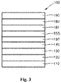
- an organic light-emitting diode comprising: a substrate; an anode electrode formed on the substrate; an organic semiconductor layer comprising a compound of formula (I), a hole transport layer, an emission layer, an electron transport layer and a cathode electrode.
- an OLED comprising: a substrate; an anode electrode formed on the substrate; an organic semiconductor layer comprising a compound of formula (I), a hole transport layer, an electron blocking layer, an emission layer, a hole blocking layer, an electron transport layer and a cathode electrode.
- an OLED comprising: a substrate; an anode electrode formed on the substrate; an organic semiconductor layer comprising a compound of formula (I), a hole transport layer, an electron blocking layer, an emission layer, a hole blocking layer, an electron transport layer, an electron injection layer, and a cathode electrode.
- OLEDs layers arranged between the above mentioned layers, on the substrate or on the top electrode.
- the OLED may comprise a layer structure of a substrate that is adjacent arranged to an anode electrode, the anode electrode is adjacent arranged to a first hole injection layer, the first hole injection layer is adjacent arranged to a first hole transport layer, the first hole transport layer is adjacent arranged to a first electron blocking layer, the first electron blocking layer is adjacent arranged to a first emission layer, the first emission layer is adjacent arranged to a first electron transport layer, the first electron transport layer is adjacent arranged to an n-type charge generation layer, the n-type charge generation layer is adjacent arranged to a hole generating layer, the hole generating layer is adjacent arranged to a second hole transport layer, the second hole transport layer is adjacent arranged to a second electron blocking layer, the second electron blocking layer is adjacent arranged to a second emission layer, between the second emission layer and the cathode electrode an optional electron transport layer and/or an optional injection layer are arranged.
- the organic semiconductor layer according to the invention may be the first hole injection layer and/or the p-type charge generation layer.
- the OLED according to Fig. 2 may be formed by a process, wherein on a substrate (110), an anode layer (120), a hole injection layer (130), a hole transport layer (140), an electron blocking layer (145), an emission layer (150), a hole blocking layer (155), an electron transport layer (160), an electron injection layer (180) and the cathode layer (190) are subsequently formed in that order.
- the organic electronic device according to the invention may be a light emitting device, or a photovoltaic cell, and preferably a light emitting device.
- the methods for deposition that can be suitable comprise:
- the method may further include forming on the anode electrode, at least one layer selected from the group consisting of forming a hole transport layer or forming a hole blocking layer, and an emission layer between the anode electrode and the first electron transport layer.
- the method may further include the steps for forming an organic light-emitting diode (OLED), wherein
- the OLED may have the following layer structure, wherein the layers having the following order: anode, organic semiconductor layer comprising a compound of formula (I) according to the invention, first hole transport layer, second hole transport layer, emission layer, optional hole blocking layer, electron transport layer, optional electron injection layer, and cathode.
- an electronic device comprising at least one organic light emitting device according to any embodiment described throughout this application, preferably, the electronic device comprises the organic light emitting diode in one of embodiments described throughout this application. More preferably, the electronic device is a display device.
- first element when a first element is referred to as being formed or disposed “on” or “onto” a second element, the first element can be disposed directly on the second element, or one or more other elements may be disposed there between.
- first element when referred to as being formed or disposed “directly on” or “directly onto” a second element, no other elements are disposed there between.
- FIG. 1 is a schematic sectional view of an organic electronic device 100, according to an exemplary embodiment of the present invention.
- the organic electronic device 100 includes a substrate 110, an anode layer 120 and a hole injection layer (HIL) (130) which may comprise a compound of formula (I).
- the HIL 130 is disposed on the anode layer 120.
- a photoactive layer (PAL) 170 and a cathode layer 190 are disposed.
- FIG. 2 is a schematic sectional view of an organic light-emitting diode (OLED) 100, according to an exemplary embodiment of the present invention.
- the OLED 100 includes a substrate 110, an anode layer 120 and a hole injection layer (HIL) 130 which may comprise a compound of formula (I).
- the HIL 130 is disposed on the anode layer 120.
- a hole transport layer (HTL) 140, an emission layer (EML) 150, an electron transport layer (ETL) 160, an electron injection layer (EIL) 180 and a cathode layer 190 are disposed.
- EML emission layer
- ETL electron transport layer
- EIL electron injection layer
- Fig. 3 is a schematic sectional view of an OLED 100, according to another exemplary embodiment of the present invention.
- Fig. 2 differs from Fig. 1 in that the OLED 100 of Fig. 2 comprises an electron blocking layer (EBL) 145 and a hole blocking layer (HBL) 155.
- EBL electron blocking layer
- HBL hole blocking layer
- the OLED 100 includes a substrate 110, an anode layer 120, a hole injection layer (HIL) 130 which may comprise a compound of formula (I), a hole transport layer (HTL) 140, an electron blocking layer (EBL) 145, an emission layer (EML) 150, a hole blocking layer (HBL) 155, an electron transport layer (ETL) 160, an electron injection layer (EIL) 180 and a cathode layer 190.
- HIL hole injection layer
- HTL hole transport layer
- EBL electron blocking layer
- EML emission layer
- HBL hole blocking layer
- ETL electron transport layer
- EIL electron injection layer
- a sealing layer may further be formed on the cathode layer 190, in order to seal the organic electronic device 100.
- various other modifications may be applied thereto.
- the invention is furthermore illustrated by the following examples which are illustrative only and non-binding.
- the HOMO and LUMO are calculated with the program package TURBOMOLE V6.5 (TURBOMOLE GmbH, Litzenhardtstrasse 19, 76135 Düsseldorf, Germany).
- the optimized geometries and the HOMO and LUMO energy levels of the molecular structures are determined by applying the hybrid functional B3LYP with a 6-31G* basis set in the gas phase. If more than one conformation is viable, the conformation with the lowest total energy is selected.
- a 15 ⁇ /cm 2 glass substrate with 90 nm ITO (available from Corning Co.) was cut to a size of 50 mm x 50 mm x 0.7 mm, ultrasonically washed with isopropyl alcohol for 5 minutes and then with pure water for 5 minutes, and washed again with UV ozone for 30 minutes, to prepare the anode layer.
- compound of formula F3 was vacuum deposited on the HIL, to form a first HTL having a thickness of 128 nm.
- N,N-bis(4-(dibenzo[b,d]furan-4-yl)phenyl)-[1,1':4',1"-terphenyl]-4-amine (CAS 1198399-61-9) was vacuum deposited on the HTL, to form an electron blocking layer (EBL) having a thickness of 5 nm.
- EBL electron blocking layer
- the hole blocking layer (HBL) is formed with a thickness of 5 nm by depositing 2-(3'-(9,9-dimethyl-9H-fluoren-2-yl)-[1,1'-biphenyl]-3-yl)-4,6-diphenyl-1,3,5-triazine on the emission layer.
- the electron transporting layer (ETL) having a thickness of 25 nm is formed on the hole blocking layer by co-depositing 50 wt.-% 4'-(4-(4-(4,6-diphenyl-1,3,5-triazin-2-yl)phenyl)naphthalen-1-yl)-[1,1'-biphenyl]-4-carbonitrile and 50 wt.-% LiQ.
- the cathode layer having a thickness of 100 nm is formed on the ETL by depositing A1 at a rate of 0.01 to 1 ⁇ /s at 10 -7 mbar.
- the OLED stack is protected from ambient conditions by encapsulation of the device with a glass slide. Thereby, a cavity is formed, which includes a getter material for further protection.
- the current efficiency is measured at 20°C.
- the current-voltage characteristic is determined using a Keithley 2635 source measure unit, by sourcing a voltage in V and measuring the current in mA flowing through the device under test. The voltage applied to the device is varied in steps of 0.1V in the range between 0V and 10V.
- the luminance-voltage characteristics and CIE coordinates are determined by measuring the luminance in cd/m 2 using an Instrument Systems CAS-140CT array spectrometer (calibrated by Deutsche Ak relie für sstelle (DAkkS)) for each of the voltage values.
- the cd/A efficiency at 10 mA/cm2 is determined by interpolating the luminance-voltage and current-voltage characteristics, respectively.
- the emission is predominately Lambertian and quantified in percent external quantum efficiency (EQE).
- EQE percent external quantum efficiency
- the efficiency EQE will be higher compared to bottom emission devices.
- the light output of the device is measured using a calibrated photodiode at 10 mA/cm 2 .
- Lifetime LT of the device is measured at ambient conditions (20°C) and 30 mA/cm 2 , using a Keithley 2400 sourcemeter, and recorded in hours.
- the brightness of the device is measured using a calibrated photo diode.
- the lifetime LT is defined as the time till the brightness of the device is reduced to 97 % of its initial value.
- C1 comparative compound
- LUMO levels were calculated with the program package TURBOMOLE V6.5 (TURBOMOLE GmbH, Litzenhardtstrasse 19, 76135 Düsseldorf, Germany) by applying the hybrid functional B3LYP with a 6-31G* basis set in the gas phase.
- Comparative compound 1 has the formula has a LUMO level of -3.81 eV.
- a more negative LUMO level is beneficial, as matrix compounds with more negative HOMO level are enabled.
- the effect on lowering the LUMO may most pronounced if if at least one X 2 , X 3 and/or X 4 are selected from CR 2 , CR 3 and/or CR 4 , wherein the substituent selected from CN, partially fluorinated or perfluorinated C 1 to C 8 alkyl, halogen, Cl or F, and/or at least one X 2 , X 3 and/or X 4 are selected from N.
- Table 1 Calculated LUMO levels of compounds of formula (I) wherein A 1 , A 2 and A 3 are selected the same A 1 , A 2 and A 3 Calculated LUMO [eV] A1 -4.43 A2 -4.41 A3 -4.45 A4 -4.63 A5 -4.73 A6 -4.7 A7 -4.73 A8 -4.62 A9 -5.14 A10 -5.14 A11 -4.85 A12 -4.65 A13 -4.95 A14 -4.87 A15 -5.14 A16 -4.53 A17 -4.78 A18 -4.71 A19 -5.02 A20 -4.98 A21 -5.16 A22 -4.96 A23 -4.24 A24 -4.39 A25 -4.31 A26 -4.46 A27 -4.85 A28 -4.65 A29 -5.26 A30 -5.04 A31 -5.12 A32 -5.38 Table 2: Calculated LUMO levels of compounds of formula (I
- Table 3 performance data for organic electroluminescent devices comprising a hole injection layer (HIL) comprising comparative and inventive compounds are shown: Table 3: Organic electronic devices comprising an hole injection layer (HIL) comprising comparative and inventive compounds.
- U at 10 mA/cm 2 [V] EQE at 10 mA/cm 2 [%] LT at 30 mA/cm 2 [h] C1 7.5 7 ⁇ 10 A5 3.9 8.9 85 A7 3.76 9.3 122 A11 3.74 9.4 129 A13 3.7 9.6 130 A14 3.73 9.5 125 A15 3.6 10.2 135 A19 3.8 9.8 128 A20 3.7 9.7 124 A29 3.5 10 123 A31 3.6 10.1 120 A33 3.8 10.4 140 A35 3.9 9.8 136 A37 4.1 9.6 127 A41 3.6 10.3 136 A47 3.7 10.5 145 A54 3.5 10.6 138 A64 3.6 9.4 120 A71 3.7 9.1 130 A75 3.5 8.9 125 A
- the operating voltage U for devices according to invention is lower than for the comparative compounds.
- a low operating voltage and/or high efficiency may be beneficial for reduced power consumption and improved battery life, in particular in mobile devices.
- a long lifetime is beneficial for long-time stability of devices.
Landscapes
- Chemical & Material Sciences (AREA)
- Organic Chemistry (AREA)
- Physics & Mathematics (AREA)
- Spectroscopy & Molecular Physics (AREA)
- Engineering & Computer Science (AREA)
- Materials Engineering (AREA)
- Electroluminescent Light Sources (AREA)
Abstract
Description
- The present invention relates to an organic compound of formula (I) for use in organic electronic devices, an organic electronic device comprising a compound of formula (I) and a display device comprising the organic electronic device
- Organic electronic devices, such as organic light-emitting diodes OLEDs, which are self-emitting devices, have a wide viewing angle, excellent contrast, quick response, high brightness, excellent operating voltage characteristics, and color reproduction. A typical OLED comprises an anode, a hole transport layer HTL, an emission layer EML, an electron transport layer ETL, and a cathode, which are sequentially stacked on a substrate. In this regard, the HTL, the EML, and the ETL are thin films formed from organic compounds.
- When a voltage is applied to the anode and the cathode, holes injected from the anode move to the EML, via the HTL, and electrons injected from the cathode move to the EML, via the ETL. The holes and electrons recombine in the EML to generate excitons. When the excitons drop from an excited state to a ground state, light is emitted. The injection and flow of holes and electrons should be balanced, so that an OLED having the above-described structure has excellent efficiency and/or a long lifetime.
- Performance of an organic light emitting diode may be affected by characteristics of the semiconductor layer, and among them, may be affected by characteristics of metal complexes which are also contained in the semiconductor layer.
- There remains a need to improve performance of organic semiconductor materials, semiconductor layers, as well as organic electronic devices thereof, in particular to achieve improved operating voltage stability over time through improving the characteristics of the compounds comprised therein.
- An aspect of the present invention provides an organic compound for use in organic electronic devices of formula (I):

- whereby A1 is selected from formula (II)

- X1 is selected from CR1;
- X2 is selected from CR2 or N;
- X3 is selected from CR3 or N;
- X4 is selected from CR4 or N;
- X5 is selected from CR5 or N;
- R1 is selected from D or H, preferably H.
- R2, R3, R4 and R5 (if present) are independently selected from CN, partially fluorinated or perfluorinated C1 to C8 alkyl, halogen, Cl, F, D or H, whereby when any of R2, R3, R4 and R5 is present, then the corresponding X2, X3, X4 and X5 is not N;
- with the proviso that either
- at least one R2 to R5 is selected from selected from CN, partially fluorinated or perfluorinated C1 to C8 alkyl, halogen, Cl, F; or
- at least one X2 to X5 is N;
- A2 and A3 are independently selected from formula (III)
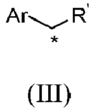
- wherein Ar is independently selected from substituted or unsubstituted C6 to C18 aryl and substituted or unsubstituted C2 to C18 heteroaryl, wherein the substituents on Ar are independently selected from CN, partially or perfluorinated C1 to C6 alkyl, halogen, Cl, F, D; and
- R' is selected from Ar, substituted or unsubstituted C6 to C18 aryl or C3 to C18 heteroaryl, partially flurorinated or perfluorinated C1 to C8 alkyl, halogen, F or CN,
- wherein the asterix "*" denotes the binding position.
- It should be noted that throughout the application and the claims any An, Bn, Rn etc. always refer to the same moieties, unless otherwise noted.
- In the present specification, when a definition is not otherwise provided, "partially fluorinated" refers to a C1 to C8 alkyl group in which only part of the hydrogen atoms are replaced by fluorine atoms.
- In the present specification, when a definition is not otherwise provided, "perfluorinated" refers to a C1 to C8 alkyl group in which all hydrogen atoms are replaced by fluorine atoms.
- In the present specification, when a definition is not otherwise provided, "substituted" refers to one substituted with a deuterium, C1 to C12 alkyl and C1 to C12 alkoxy.
- However, in the present specification "aryl substituted" refers to a substitution with one or more aryl groups, which themselves may be substituted with one or more aryl and/or heteroaryl groups.
- Correspondingly, in the present specification "heteroaryl substituted" refers to a substitution with one or more heteroaryl groups, which themselves may be substituted with one or more aryl and/or heteroaryl groups.
- In the present specification, when a definition is not otherwise provided, an "alkyl group" refers to a saturated aliphatic hydrocarbyl group. The alkyl group may be a C1 to C12 alkyl group. More specifically, the alkyl group may be a C1 to C10 alkyl group or a C1 to C6 alkyl group. For example, a C1 to C4 alkyl group includes 1 to 4 carbons in alkyl chain, and may be selected from methyl, ethyl, propyl, iso-propyl, n-butyl, iso-butyl, sec-butyl, and tert-butyl.
- Specific examples of the alkyl group may be a methyl group, an ethyl group, a propyl group, an isopropyl group, a butyl group, an iso-butyl group, a sec-butyl group, a tert-butyl group, a pentyl group, a hexyl group.
- The term "cycloalkyl" refers to saturated hydrocarbyl groups derived from a cycloalkane by formal abstraction of one hydrogen atom from a ring atom comprised in the corresponding cycloalkane. Examples of the cycloalkyl group may be a cyclopropyl group, a cyclobutyl group, a cyclopentyl group, a cyclohexyl group, a methylcyclohexyl group, an adamantly group and the like.
- The term "hetero" is understood the way that at least one carbon atom, in a structure which may be formed by covalently bound carbon atoms, is replaced by another polyvalent atom. Preferably, the heteroatoms are selected from B, Si, N, P, O, S; more preferably from N, P, O, S.
- In the present specification, "aryl group" refers to a hydrocarbyl group which can be created by formal abstraction of one hydrogen atom from an aromatic ring in the corresponding aromatic hydrocarbon. Aromatic hydrocarbon refers to a hydrocarbon which contains at least one aromatic ring or aromatic ring system. Aromatic ring or aromatic ring system refers to a planar ring or ring system of covalently bound carbon atoms, wherein the planar ring or ring system comprises a conjugated system of delocalized electrons fulfilling Hückel's rule. Examples of aryl groups include monocyclic groups like phenyl or tolyl, polycyclic groups which comprise more aromatic rings linked by single bonds, like biphenyl, and polycyclic groups comprising fused rings, like naphtyl or fluoren-2-yl.
- Analogously, under heteroaryl, it is especially where suitable understood a group derived by formal abstraction of one ring hydrogen from a heterocyclic aromatic ring in a compound comprising at least one such ring.
- Under heterocycloalkyl, it is especially where suitable understood a group derived by formal abstraction of one ring hydrogen from a saturated cycloalkyl ring in a compound comprising at least one such ring.
- The term "fused aryl rings" or "condensed aryl rings" is understood the way that two aryl rings are considered fused or condensed when they share at least two common sp2-hybridized carbon atoms
- In the present specification, the single bond refers to a direct bond.
- The term "free of", "does not contain", "does not comprise" does not exclude impurities which may be present in the compounds prior to deposition. Impurities have no technical effect with respect to the object achieved by the present invention.
- The term "contacting sandwiched" refers to an arrangement of three layers whereby the layer in the middle is in direct contact with the two adjacent layers.
- The terms "light-absorbing layer" and "light absorption layer" are used synonymously.
- The terms "light-emitting layer", "light emission layer" and "emission layer" are used synonymously.
- The terms "OLED", "organic light-emitting diode" and "organic light-emitting device" are used synonymously.
- The terms "anode", "anode layer" and "anode electrode" are used synonymously.
- The terms "cathode", "cathode layer" and "cathode electrode" are used synonymously.
- In the specification, hole characteristics refer to an ability to donate an electron to form a hole when an electric field is applied and that a hole formed in the anode may be easily injected into the emission layer and transported in the emission layer due to conductive characteristics according to a highest occupied molecular orbital (HOMO) level.
- In addition, electron characteristics refer to an ability to accept an electron when an electric field is applied and that electrons formed in the cathode may be easily injected into the emission layer and transported in the emission layer due to conductive characteristics according to a lowest unoccupied molecular orbital (LUMO) level.
- Surprisingly, it was found that the organic compound of the present invention solves the problem underlying the present invention by enabling devices in various aspects superior over the organic electroluminescent devices known in the art, in particular with respect to operating voltage over lifetime.
- According to one embodiment of the present invention, the compound is selected of the formula (IV)


According to one embodiment of the present invention, either R1 and/or R5 are independently selected from CN or CF3, or at least one Rn and Rn+1 (with n= 1 to 4) are independently selected from CN or CF3. - According to one embodiment of the present invention, A1 and A3 are not identical.
- Alternatively, according to one embodiment of the present invention, at least one from A2 and A3 is identical to A1.
- According to one embodiment of the present invention, A1 and A2 may be selected the same or differently and A1 and A3 are not identical.
- According to one embodiment of the present invention, A1 and A2 are identical and A1 and A3 are not identical.
- According to one embodiment of the present invention, A1, A2 and A3 are identical.
- According to one embodiment of the present invention, A1, A2 and A3 are identical and not selected from any of the following moieties:


- According to one embodiment of the present invention, X2, X3 and/or X4 are selected from CN or N; preferably X2, X3 and/or X4 are selected from CN or N and at least one remaining Rn, wherein n is 2 to 5, is selected from halogen, Cl or F.
- According to one embodiment of the present invention, X2, X3 and/or X4 are selected from perfluorinated C1 to C8 alkyl and at least one remaining Rn, wherein n is an integer from 2 to 5, is selected from halogen, Cl or F; preferably at least two remaining Rn, wherein n is an integer from 2 to 5, are selected from halogen, Cl or F.
- According to one embodiment of the present invention, X3 is selected from N or CR3, wherein R3 is selected from CN, partially flurorinated or perfluorinated C1 to C8 alkyl.
- According to one embodiment of the present invention, R2 and/or R3 are selected from CN, or partially flurorinated or perfluorinated C1 to C8 alkyl.
- According to one embodiment of the present invention, one of R2 and R3 is selected from CN, partially flurorinated or perfluorinated C1 to C8 alkyl and at least one out of R2 to R5 is independently selected from CN, partially flurorinated or perfluorinated C1 to C8 alkyl, halogen, Cl, F.
- According to one embodiment of the present invention, R5 is D or H, preferably H.
- According to one embodiment of the present invention, at least two out of R2 to R5 are independently selected from halogen, Cl, F.
- According to one embodiment of the present invention, at least three out of R2 to R5 are independently selected from CN, partially flurorinated or perfluorinated C1 to C8 alkyl, halogen, Cl, F.
- According to one embodiment of the present invention, three R2 to R5 are independently selected from CN, partially flurorinated or perfluorinated C1 to C8 alkyl, halogen, Cl, F.
- According to one embodiment of the present invention one of X2 to X5 is N and one of R2 to R5 is independently selected from CN, partially flurorinated or perfluorinated C1 to C8 alkyl, halogen, Cl, F.
- According to one embodiment of the present invention, one of X2 and X5 is N and one of R2 to R5 is independently selected from CN, partially flurorinated or perfluorinated C1 to C8 alkyl, halogen, Cl, F.
- According to one embodiment of the present invention, A1 and A3 are not identical, and in A3 Ar is selected from substituted C6 to C12 aryl or substituted C2 to C12 heteroaryl, wherein at least one substituent on Ar is independently selected from CN or perfluorinated C1 to C6 alkyl, and at least two substituents are selected from halogen, Cl, F; preferably Ar is selected from substituted phenyl or from group consisting of pyridyl or pyrimidyl, wherein at least one substituent on Ar is independently selected from CN or perfluorinated C1 to C6 alkyl, and at least two substituents are selected from halogen, Cl, F.
- According to one embodiment of the present invention, A1 and A3 are not identical, and in A3 Ar is selected from substituted C6 to C12 aryl or substituted C2 to C12 heteroaryl, wherein the substituents on Ar are independently selected from CN, perfluorinated C1 to C6 alkyl, halogen, Cl, F; preferably Ar is selected from substituted phenyl or from group consisting of pyridyl or pyrimidyl, wherein the substituents on Ar are independently selected from CN, perfluorinated C1 to C6 alkyl, halogen, Cl, F.
- According to one embodiment of the present invention, A1 and A2 are not identical, whereas A2 and A3 are identical and in A2 and A3 Ar is selected from substituted C6 to C12 aryl or substituted C2 to C12 heteroaryl, wherein the substituents on Ar are independently selected from CN, perfluorinated C1 to C6 alkyl, halogen, Cl, F; preferably Ar is selected from substituted phenyl or from group consisting of pyridyl or pyrimidyl, wherein the substituents on Ar are independently selected from CN, perfluorinated C1 to C6 alkyl, halogen, Cl, F.
- According to one embodiment of the present invention, A1 and A2 are identical and A1 and A3 are not identical; and in A3 Ar is selected from substituted C6 to C12 aryl or substituted C2 to C12 heteroaryl, wherein the substituents on Ar are independently selected from CN, perfluorinated C1 to C6 alkyl, halogen, Cl, F; preferably Ar is selected from substituted phenyl or from group consisting of pyridyl or pyrimidyl, wherein the substituents on Ar are independently selected from CN, perfluorinated C1 to C6 alkyl, halogen, Cl, F.
- According to one embodiment of the present invention R' is selected CN.
- According to one embodiment of the present invention, formula (II) is selected from the group comprising the following moieties:





- According to one embodiment of the present invention, formula (II) does not include the following moieties:


- According to one embodiment of the present invention, formula (III) is selected from the group comprising the following moieties:


- According to one embodiment of the present invention, formula (III) does not include the following moieties:


- According to one embodiment of the present invention, the LUMO level of compound of formula (I) is selected in the range of ≤ -4.4 eV and ≥ -5.3 eV when calculated with the program package TURBOMOLE V6.5 (TURBOMOLE GmbH, Litzenhardtstrasse 19, 76135 Karlsruhe, Germany) by applying the hybrid functional B3LYP with a 6-31G* basis set in the gas phase, preferably in the range of ≤ -4.5 eV and ≥ -5.25 eV and most preferred in the range of ≤ -4.7 eV and ≥ -5.25 eV.
- According to one embodiment of the present invention, wherein in compound of formula (I) A1, A2 and A3 may be selected the same and the LUMO level of compound of formula (I) is selected in the range of ≤ -4.7 eV and ≥ -5.3 eV when calculated with the program package TURBOMOLE V6.5 (TURBOMOLE GmbH, Litzenhardtstrasse 19, 76135 Karlsruhe, Germany) by applying the hybrid functional B3LYP with a 6-31G* basis set in the gas phase, preferably in the range of ≤ -4.72 eV and ≥ -5.25 eV and most preferred in the range of ≤ -4.75 eV and ≥ -5.25 eV.
- According to one embodiment of the present invention, wherein in compound of formula (I) A1 and A2 may be selected the same or differently and A1 is not identical to A3 and the LUMO level of compound of formula (I) is selected in the range of ≤ -4.5 eV and ≥ -5.3 eV when calculated with the program package TURBOMOLE V6.5 (TURBOMOLE GmbH, Litzenhardtstrasse 19, 76135 Karlsruhe, Germany) by applying the hybrid functional B3LYP with a 6-31G* basis set in the gas phase, preferably in the range of ≤ -4.6 eV and ≥ -5.25 eV and most preferred in the range of ≤ -4.7 eV and ≥ -5.25 eV.
- According to one embodiment of the present invention, wherein in compound of formula (I) A1, A2 and A3 may be selected the same and the LUMO level of compound of formula (I) is selected in the range of ≤ -4.7 eV and ≥ -5.3 eV when calculated with the program package TURBOMOLE V6.5 (TURBOMOLE GmbH, Litzenhardtstrasse 19, 76135 Karlsruhe, Germany) by applying the hybrid functional B3LYP with a 6-31G* basis set in the gas phase, preferably in the range of ≤ -4.72 eV and ≥ -5.25 eV and most preferred in the range of ≤ -4.75 eV and ≥ -5.25 eV; and X2, X3 and/or X4 are selected from CN or N; preferably X2, X3 and/or X4 are selected from CN or N and at least one remaining Rn, wherein n is 2 to 5, is selected from halogen, Cl or F; or X2, X3 and/or X4 are selected from perfluorinated C1 to C8 alkyl and at least one remaining Rn, wherein n is an integer from 2 to 5, is selected from halogen, Cl or F; preferably at least two remaining Rn, wherein n is an integer from 2 to 5, are selected from halogen, Cl or F.
- According to one embodiment of the present invention, wherein in compound of formula (I) A1 and A2 may be selected the same or differently and A3 is not identical to A3 and the LUMO level of compound of formula (I) is selected in the range of ≤ -4.5 eV and ≥ -5.3 eV when calculated with the program package TURBOMOLE V6.5 (TURBOMOLE GmbH, Litzenhardtstrasse 19, 76135 Karlsruhe, Germany) by applying the hybrid functional B3LYP with a 6-31G* basis set in the gas phase, preferably in the range of ≤ - 4.6 eV and ≥ -5.25 eV and most preferred in the range of ≤ -4.7 eV and ≥ -5.25 eV; and X2, X3 and/or X4 are selected from CN or N; preferably X2, X3 and/or X4 are selected from CN or N and at least one remaining Rn, wherein n is 2 to 5, is selected from halogen, Cl or F; or X2, X3 and/or X4 are selected from perfluorinated C1 to C8 alkyl and at least one remaining Rn, wherein n is an integer from 2 to 5, is selected from halogen, Cl or F; preferably at least two remaining Rn, wherein n is an integer from 2 to 5, are selected from halogen, Cl or F.
- According to one embodiment, the compound of formula (I) is selected from the compounds A1 to A101:
A1 A2 A3 A1 


A2 


A3 


A4 


A5 


A6 


A7 

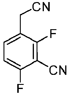
A8 


A9 


A10 


A11 


A12 


A13 


A14 


A15 


A16 


A17 


A18 


A19 


A20 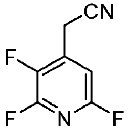


A21 


A22 


A23 


A24 


A25 


A26 


A27 


A28 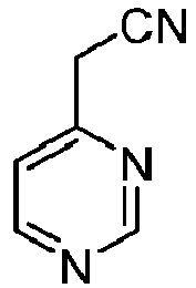


A29 


A30 


A31 


A32 
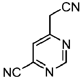

A33 


A34 


A35 


A36 


A37 
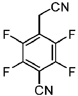

A38 


A39 
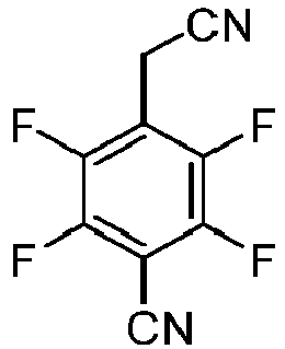

A40 


A41 


A42 


A43 


A44 


A45 


A46 


A47 


A48 
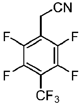

A49 


A50 


A51 


A52 


A53 


A54 


A55 
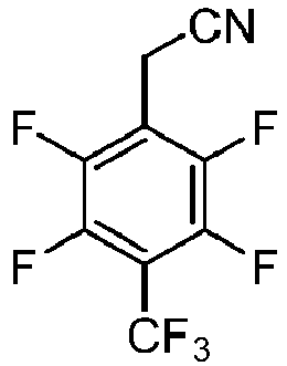

A56 


A57 
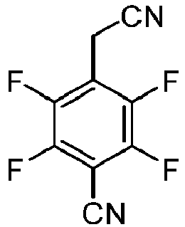
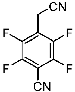
A58 


A59 


A60 


A61 


A62 


A63 


A64 


A65 


A66 


A67 


A68 


A69 


A70 


A71 


A72 


A73 


A74 


A75 

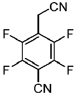
A76 


A77 


A78 


A79 


A80 


A81 


A82 


A83 


A84 


A85 


A86 


A87 


A88 


A89 


A90 


A91 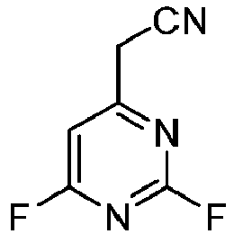


A92 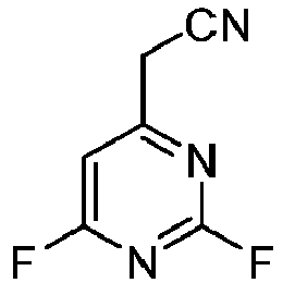


A93 


A94 


A95 


A96 


A97 


A98 


A99 


A100 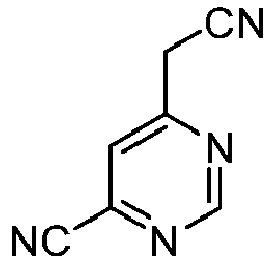


A101 
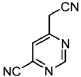

- The present invention furthermore relates to an organic electronic device comprising an anode layer, a cathode layer and at least one organic semiconductor layer, wherein the at least one organic semiconductor layer is arranged between the anode layer and the cathode layer; and wherein the at least one organic semiconductor layer comprises a compound of formula (I)
- According to one embodiment, the organic semiconductor layer comprises a composition comprising a compound of formula (IV) and at least one compound of formula (IVa) to (IVd)


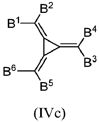

- In case the organic semiconductor layer comprises such a composition, throughout this application text the term "compound of formula (I)" shall also intend to include the composition as described above.
- According to one embodiment of the present invention the organic semiconductor layer and/or the compound of formula (I) are non-emissive.
- In the context of the present specification the term "essentially non-emissive" or "non-emissive" means that the contribution of the compound or layer to the visible emission spectrum from the device is less than 10 %, preferably less than 5 % relative to the visible emission spectrum. The visible emission spectrum is an emission spectrum with a wavelength of about ≥ 380 nm to about ≤ 780 nm.
- According to one embodiment of the invention, the at least one organic semiconductor layer further comprises a substantially covalent matrix compound.
- The organic semiconductor layer may further comprises a substantially covalent matrix compound. According to one embodiment the substantially covalent matrix compound may be selected from at least one organic compound. The substantially covalent matrix may consists substantially from covalently bound C, H, O, N, S, which optionally comprise in addition covalently bound B, P, As and/or Se.
- According to one embodiment of the organic electronic device, the organic semiconductor layer further comprises a substantially covalent matrix compound, wherein the substantially covalent matrix compound may be selected from organic compounds consisting substantially from covalently bound C, H, O, N, S, which optionally comprise in addition covalently bound B, P, As and/or Se.
- Organometallic compounds comprising covalent bonds carbon-metal, metal complexes comprising organic ligands and metal salts of organic acids are further examples of organic compounds that may serve as substantially covalent matrix compounds of the hole injection layer.
- In one embodiment, the substantially covalent matrix compound lacks metal atoms and majority of its skeletal atoms may be selected from C, O, S, N. Alternatively, the substantially covalent matrix compound lacks metal atoms and majority of its skeletal atoms may be selected from C and N.
- According to one embodiment, the substantially covalent matrix compound may have a molecular weight Mw of ≥ 400 and ≤ 2000 g/mol, preferably a molecular weight Mw of ≥ 450 and ≤ 1500 g/mol, further preferred a molecular weight Mw of ≥ 500 and ≤ 1000 g/mol, in addition preferred a molecular weight Mw of ≥ 550 and ≤ 900 g/mol, also preferred a molecular weight Mw of ≥ 600 and ≤ 800 g/mol.
- Preferably, the substantially covalent matrix compound comprises at least one arylamine moiety, alternatively a diarylamine moiety, alternatively a triarylamine moiety.
- Preferably, the substantially covalent matrix compound is free of metals and/or ionic bonds.
- According to another aspect of the present invention, the at least one matrix compound, also referred to as "substantially covalent matrix compound", may comprises at least one arylamine compound, diarylamine compound, triarylamine compound, a compound of formula (VI) or a compound of formula (VII):

- T1, T2, T3, T4 and T5 are independently selected from a single bond, phenylene, biphenylene, terphenylene or naphthenylene, preferably a single bond or phenylene;
- T6 is phenylene, biphenylene, terphenylene or naphthenylene;
- Ar1, Ar2, Ar3, Ar4 and Ar5 are independently selected from substituted or unsubstituted C6 to C20 aryl, or substituted or unsubstituted C3 to C20 heteroarylene, substituted or unsubstituted biphenylene, substituted or unsubstituted fluorene, substituted 9-fluorene, substituted 9,9-fluorene, substituted or unsubstituted naphthalene, substituted or unsubstituted anthracene, substituted or unsubstituted phenanthrene, substituted or unsubstituted pyrene, substituted or unsubstituted perylene, substituted or unsubstituted triphenylene, substituted or unsubstituted tetracene, substituted or unsubstituted tetraphene, substituted or unsubstituted dibenzofurane, substituted or unsubstituted dibenzothiophene, substituted or unsubstituted xanthene, substituted or unsubstituted carbazole, substituted 9-phenylcarbazole, substituted or unsubstituted azepine, substituted or unsubstituted dibenzo[b,f]azepine, substituted or unsubstituted 9,9'-spirobi[fluorene], substituted or unsubstituted spiro[fluorene-9,9'-xanthene], or a substituted or unsubstituted aromatic fused ring system comprising at least three substituted or unsubstituted aromatic rings selected from the group comprising substituted or unsubstituted non-hetero, substituted or unsubstituted hetero 5-member rings, substituted or unsubstituted 6-member rings and/or substituted or unsubstituted 7-member rings, substituted or unsubstituted fluorene, or a fused ring system comprising 2 to 6 substituted or unsubstituted 5- to 7-member rings and the rings are selected from the group comprising (i) unsaturated 5- to 7-member ring of a heterocycle, (ii) 5- to 6-member of an aromatic heterocycle, (iii) unsaturated 5- to 7-member ring of a non-heterocycle, (iv) 6-member ring of an aromatic non-heterocycle;
- wherein
- the substituents of Ar1, Ar2, Ar3, Ar4 and Ar5 are selected the same or different from the group comprising H, D, F, C(-O)R2, CN, Si(R2)3, P(-O)(R2)2, OR2, S(-O)R2, S(-O)2R2, substituted or unsubstituted straight-chain alkyl having 1 to 20 carbon atoms, substituted or unsubstituted branched alkyl having 1 to 20 carbon atoms, substituted or unsubstituted cyclic alkyl having 3 to 20 carbon atoms, substituted or unsubstituted alkenyl or alkynyl groups having 2 to 20 carbon atoms, substituted or unsubstituted alkoxy groups having 1 to 20 carbon atoms, substituted or unsubstituted aromatic ring systems having 6 to 40 aromatic ring atoms, and substituted or unsubstituted heteroaromatic ring systems having 5 to 40 aromatic ring atoms, unsubstituted C6 to C18 aryl, unsubstituted C3 to C18 heteroaryl, a fused ring system comprising 2 to 6 unsubstituted 5- to 7-member rings and the rings are selected from the group comprising unsaturated 5- to 7-member ring of a heterocycle, 5- to 6-member of an aromatic heterocycle, unsaturated 5- to 7-member ring of a non-heterocycle, and 6-member ring of an aromatic non-heterocycle,
- wherein R2 may be selected from H, D, straight-chain alkyl having 1 to 6 carbon atoms, branched alkyl having 1 to 6 carbon atoms, cyclic alkyl having 3 to 6 carbon atoms, alkenyl or alkynyl groups having 2 to 6 carbon atoms, C6 to C18 aryl or C3 to C18 heteroaryl.
- According to an embodiment wherein T1, T2, T3, T4 and T5 may be independently selected from a single bond, phenylene, biphenylene or terphenylene. According to an embodiment wherein T1, T2, T3, T4 and T5 may be independently selected from phenylene, biphenylene or terphenylene and one of T1, T2, T3, T4 and T5 are a single bond. According to an embodiment wherein T1, T2, T3, T4 and T5 may be independently selected from phenylene or biphenylene and one of T1, T2, T3, T4 and T5 are a single bond. According to an embodiment wherein T1, T2, T3, T4 and T5 may be independently selected from phenylene or biphenylene and two of T1, T2, T3, T4 and T5 are a single bond.
- According to an embodiment wherein T1, T2 and T3 may be independently selected from phenylene and one of T1, T2 and T3 are a single bond. According to an embodiment wherein T1, T2 and T3 may be independently selected from phenylene and two of T1, T2 and T3 are a single bond.
- According to an embodiment wherein T6 may be phenylene, biphenylene, terphenylene. According to an embodiment wherein T6 may be phenylene. According to an embodiment wherein T6 may be biphenylene. According to an embodiment wherein T6 may be terphenylene.
- According to an embodiment wherein Ar1, Ar2, Ar3, Ar4 and Ar5 may be independently selected from D1 to D16:


- According to an embodiment, wherein Ar1, Ar2, Ar3, Ar4 and Ar5 may be independently selected from D1 to D15; alternatively selected from D1 to D10 and D13 to D15.
- According to an embodiment, wherein Ar1, Ar2, Ar3, Ar4 and Ar5 may be independently selected from the group consisting of D1, D2, D5, D7, D9, D10, D13 to D16.
- The rate onset temperature may be in a range particularly suited to mass production, when Ar1, Ar2, Ar3, Ar4 and Ar5 are selected in this range.
- The "matrix compound of formula (VI) or formula (VII)" may be also referred to as "hole transport compound".
- According to one embodiment, the substantially covalent matrix compound comprises at least one naphthyl group, carbazole group, dibenzofurane group, dibenzothiophene group and/or substituted fluorenyl group, wherein the substituents are independently selected from methyl, phenyl or fluorenyl.
- According to an embodiment of the electronic device, wherein the matrix compound of formula (VI) or formula (VII) are selected from F1 to F19:


- The organic semiconductor layer may be formed on the anode layer or cathode layer by vacuum deposition, spin coating, printing, casting, slot-die coating, Langmuir-Blodgett (LB) deposition, or the like. When the Organic semiconductor layer is formed using vacuum deposition, the deposition conditions may vary according to the compound(s) that are used to form the layer, and the desired structure and thermal properties of the layer. In general, however, conditions for vacuum deposition may include a deposition temperature of 100° C to 350° C, a pressure of 10-8 to 10-3 Torr (1 Torr equals 133.322 Pa), and a deposition rate of 0.1 to 10 nm/sec.
- When the organic semiconductor layer is formed using spin coating or printing, coating conditions may vary according to the compound(s) that are used to form the layer, and the desired structure and thermal properties of the organic semiconductor layer. For example, the coating conditions may include a coating speed of about 2000 rpm to about 5000 rpm, and a thermal treatment temperature of about 80° C to about 200° C. Thermal treatment removes a solvent after the coating is performed.
- The thickness of the organic semiconductor layer may be in the range from about 1 nm to about 20 nm, and for example, from about 2 nm to about 15 nm, alternatively about 2 nm to about 12 nm.
- When the thickness of the organic semiconductor layer is within this range, the organic semiconductor layer may have excellent hole injecting and/or hole generation characteristics, without a substantial penalty in driving voltage.
- According to one embodiment of the present invention, the organic semiconductor layer may comprise:
- at least about ≥ 0.5 wt.-% to about ≤ 30 wt.-%, preferably about ≥ 0.5 wt.-% to about ≤ 20 wt.-%, and more preferred about ≥ 1 wt.-% to about ≤ 15 wt.-% of a compound of formula (I), and
- at least about ≥ 70 wt.-% to about ≤ 99.5 wt.-%, preferably about ≥ 80 wt.-% to about ≤ 99.5 wt.-%, and more preferred about ≥ 85 wt.-% to about ≤ 99 wt.-% of a substantially covalent matrix compound; preferably the wt.-% of the compound of formula (I) is lower than the wt.-% of the substantially covalent matrix compound; wherein the weight-% of the components are based on the total weight of the organic semiconductor layer.
- According to one embodiment of the invention, the organic electronic device comprises at least one photoactive layer and the at least one of the at least one organic semiconductor layers is arranged between the anode and the at least one photoactive layer.
- According to one embodiment of the invention, the organic electronic device comprises at least two photoactive layers, wherein at least one of the at least one organic semiconductor layers is arranged between the first and the second photoactive layer.
- According to one embodiment of the invention, the organic electronic devices comprises at least one photoactive layer, wherein the photoactive layer is arranged between the anode layer and the cathode layer.
- According to one embodiment of the invention, the organic electronic devices comprises at least one photoactive layer and the at least one organic semiconductor layers is arranged between the anode and the at least one photoactive layer.
- According to one embodiment of the invention, the organic electronic device comprises at least two photoactive layers, wherein at least one of the at least one organic semiconductor layers is arranged between the first and the second photoactive layer.
- According to one embodiment of the invention, the organic electronic device comprises at least two photoactive layers, wherein one of the at least one organic semiconductor layers is arranged between the first and the second photoactive layer and one of the at least one organic semiconductor layers is arranged between the anode layer and the first photoactive layer.
- According to one embodiment of the invention the electronic organic device is an electroluminescent device, preferably an organic light emitting diode.
- The present invention furthermore relates to a display device comprising an organic electronic device according to the present invention.
- In accordance with the invention, the organic electronic device may comprise, besides the layers already mentioned above, further layers. Exemplary embodiments of respective layers are described in the following:
- The substrate may be any substrate that is commonly used in manufacturing of, electronic devices, such as organic light-emitting diodes. If light is to be emitted through the substrate, the substrate shall be a transparent or semitransparent material, for example a glass substrate or a transparent plastic substrate. If light is to be emitted through the top surface, the substrate may be both a transparent as well as a non-transparent material, for example a glass substrate, a plastic substrate, a metal substrate or a silicon substrate.
- The anode layer may be formed by depositing or sputtering a material that is used to form the anode layer. The material used to form the anode layer may be a high work-function material, so as to facilitate hole injection. The anode material may also be selected from a low work function material (i.e. aluminum). The anode electrode may be a transparent or reflective electrode. Transparent conductive oxides, such as indium tin oxide (ITO), indium zinc oxide (IZO), tin-dioxide (SnO2), aluminum zinc oxide (AlZO) and zinc oxide (ZnO), may be used to form the anode electrode. The anode layer may also be formed using metals, typically silver (Ag), gold (Au), or metal alloys.
- A hole injection layer (HIL) may be formed on the anode layer by vacuum deposition, spin coating, printing, casting, slot-die coating, Langmuir-Blodgett (LB) deposition, or the like. When the HIL is formed using vacuum deposition, the deposition conditions may vary according to the compound that is used to form the HIL, and the desired structure and thermal properties of the HIL. In general, however, conditions for vacuum deposition may include a deposition temperature of 100° C to 500° C, a pressure of 10-8 to 10-3 Torr (1 Torr equals 133.322 Pa), and a deposition rate of 0.1 to 10 nm/sec.
- When the HIL is formed using spin coating or printing, coating conditions may vary according to the compound that is used to form the HIL, and the desired structure and thermal properties of the HIL. For example, the coating conditions may include a coating speed of about 2000 rpm to about 5000 rpm, and a thermal treatment temperature of about 80° C to about 200° C. Thermal treatment removes a solvent after the coating is performed.
- The HIL may be formed of any compound that is commonly used to form a HIL. Examples of compounds that may be used to form the HIL include a phthalocyanine compound, such as copper phthalocyanine (CuPc), 4,4',4"-tris (3-methylphenylphenylamino) triphenylamine (m-MTDATA), TDATA, 2T-NATA, polyaniline/dodecylbenzenesulfonic acid (Pani/DBSA), poly(3,4-ethylenedioxythiophene)/poly(4-styrenesulfonate) (PEDOT/PSS), polyaniline/camphor sulfonic acid (Pani/CSA), and polyaniline)/poly(4-styrenesulfonate (PANI/PSS).
- The HIL may comprise or consist of p-type dopant and the p-type dopant may be selected from tetrafluoro-tetracyanoquinonedimethane (F4TCNQ), 2,2'-(perfluoronaphthalen-2,6-diylidene) dimalononitrile or 2,2',2"-(cyclopropane-1,2,3-triylidene)tris(2-(p-cyanotetrafluorophenyl)acetonitrile) but not limited hereto. The HIL may be selected from a hole-transporting matrix compound doped with a p-type dopant. Typical examples of known doped hole transport materials are: copper phthalocyanine (CuPc), which HOMO level is approximately -5.2 eV, doped with tetrafluoro-tetracyanoquinonedimethane (F4TCNQ), which LUMO level is about -5.2 eV; zinc phthalocyanine (ZnPc) (HOMO = -5.2 eV) doped with F4TCNQ; α-NPD (N,N'-Bis(naphthalen-1-yl)-N,N'-bis(phenyl)-benzidine) doped with F4TCNQ. α-NPD doped with 2,2'-(perfluoronaphthalen-2,6-diylidene) dimalononitrile. The p-type dopant concentrations can be selected from 1 to 20 wt.-%, more preferably from 3 wt.-% to 10 wt.-%.
- The thickness of the HIL may be in the range from about 1 nm to about 100 nm, and for example, from about 1 nm to about 25 nm. When the thickness of the HIL is within this range, the HIL may have excellent hole injecting characteristics, without a substantial penalty in driving voltage.
- A hole transport layer (HTL) may be formed on the HIL by vacuum deposition, spin coating, slot-die coating, printing, casting, Langmuir-Blodgett (LB) deposition, or the like. When the HTL is formed by vacuum deposition or spin coating, the conditions for deposition and coating may be similar to those for the formation of the HIL. However, the conditions for the vacuum or solution deposition may vary, according to the compound that is used to form the HTL.
- The HTL may be formed of any compound that is commonly used to form a HTL. Compounds that can be suitably used are disclosed for example in Yasuhiko Shirota and Hiroshi Kageyama, Chem. Rev. 2007, 107, 953-1010 and incorporated by reference. Examples of the compound that may be used to form the HTL are: carbazole derivatives, such as N-phenylcarbazole or polyvinylcarbazole; benzidine derivatives, such as N,N'-bis(3-methylphenyl)-N,N'-diphenyl-[1,1-biphenyl]-4,4'-diamine (TPD), or N,N'-di(naphthalen-1-yl)-N,N'-diphenyl benzidine (alpha-NPD); and triphenylamine-based compound, such as 4,4',4"-tris(N-carbazolyl)triphenylamine (TCTA). Among these compounds, TCTA can transport holes and inhibit excitons from being diffused into the EML
- According to one embodiment of the present invention, the hole transport layer may comprise the same substantially covalent matrix compound as the organic semiconductor layer of the present invention.
- The thickness of the HTL may be in the range of about 5 nm to about 250 nm, preferably, about 10 nm to about 200 nm, further about 20 nm to about 190 nm, further about 40 nm to about 180 nm, further about 60 nm to about 170 nm, further about 80 nm to about 160 nm, further about 100 nm to about 160 nm, further about 120 nm to about 140 nm. A preferred thickness of the HTL may be 170 nm to 200 nm.
- When the thickness of the HTL is within this range, the HTL may have excellent hole transporting characteristics, without a substantial penalty in driving voltage.
- The function of an electron blocking layer (EBL) is to prevent electrons from being transferred from an emission layer to the hole transport layer and thereby confine electrons to the emission layer. Thereby, efficiency, operating voltage and/or lifetime are improved. Typically, the electron blocking layer comprises a triarylamine compound. The triarylamine compound may have a LUMO level closer to vacuum level than the LUMO level of the hole transport layer. The electron blocking layer may have a HOMO level that is further away from vacuum level compared to the HOMO level of the hole transport layer. The thickness of the electron blocking layer may be selected between 2 and 20 nm.
- If the electron blocking layer has a high triplet level, it may also be described as triplet control layer.
- The function of the triplet control layer is to reduce quenching of triplets if a phosphorescent green or blue emission layer is used. Thereby, higher efficiency of light emission from a phosphorescent emission layer can be achieved. The triplet control layer is selected from triarylamine compounds with a triplet level above the triplet level of the phosphorescent emitter in the adjacent emission layer. Suitable compounds for the triplet control layer, in particular the triarylamine compounds, are described in
EP 2 722 908 A1 . - The photoactive layer converts an electrical current into photons or photons into an electrical current.
- The PAL may be formed on the HTL by vacuum deposition, spin coating, slot-die coating, printing, casting, LB deposition, or the like. When the PAL is formed using vacuum deposition or spin coating, the conditions for deposition and coating may be similar to those for the formation of the HIL. However, the conditions for deposition and coating may vary, according to the compound that is used to form the PAL.
- According to one embodiment of the present invention, the photoactive layer does not comprise the compound of formula (I).
- The photoactive layer may be a light-emitting layer or a light-absorbing layer.
- The EML may be formed on the HTL by vacuum deposition, spin coating, slot-die coating, printing, casting, LB deposition, or the like. When the EML is formed using vacuum deposition or spin coating, the conditions for deposition and coating may be similar to those for the formation of the HIL. However, the conditions for deposition and coating may vary, according to the compound that is used to form the EML.
- According to one embodiment of the present invention, the emission layer does not comprise the compound of formula (I).
- The emission layer (EML) may be formed of a combination of a host and an emitter dopant. Example of the host are Alq3, 4,4'-N,N'-dicarbazole-biphenyl (CBP), poly(n-vinylcarbazole) (PVK), 9,10-di(naphthalene-2-yl)anthracene (ADN), 4,4',4"-tris(carbazol-9-yl)-triphenylamine(TCTA), 1,3,5-tris(N-phenylbenzimidazole-2-yl)benzene (TPBI), 3-tert-butyl-9,10-di-2-naphthylanthracenee (TBADN), distyrylarylene (DSA) and bis(2-(2-hydroxyphenyl)benzo-thiazolate)zinc (Zn(BTZ)2).
- The emitter dopant may be a phosphorescent or fluorescent emitter. Phosphorescent emitters and emitters which emit light via a thermally activated delayed fluorescence (TADF) mechanism may be preferred due to their higher efficiency. The emitter may be a small molecule or a polymer.
- Examples of red emitter dopants are PtOEP, Ir(piq)3, and Btp2lr(acac), but are not limited thereto. These compounds are phosphorescent emitters, however, fluorescent red emitter dopants could also be used.
- Examples of phosphorescent green emitter dopants are Ir(ppy)3 (ppy = phenylpyridine), Ir(ppy)2(acac), Ir(mpyp)3.
- Examples of phosphorescent blue emitter dopants are F2Irpic, (F2ppy)2Ir(tmd) and Ir(dfppz)3 and ter-fluorene. 4.4'-bis(4-diphenyl amiostyryl)biphenyl (DPAVBi), 2,5,8,11-tetra-tert-butyl perylene (TBPe) are examples of fluorescent blue emitter dopants.
- The amount of the emitter dopant may be in the range from about 0.01 to about 50 parts by weight, based on 100 parts by weight of the host. Alternatively, the emission layer may consist of a light-emitting polymer. The EML may have a thickness of about 10 nm to about 100 nm, for example, from about 20 nm to about 60 nm. When the thickness of the EML is within this range, the EML may have excellent light emission, without a substantial penalty in driving voltage.
- A hole blocking layer (HBL) may be formed on the EML, by using vacuum deposition, spin coating, slot-die coating, printing, casting, LB deposition, or the like, in order to prevent the diffusion of holes into the ETL. When the EML comprises a phosphorescent dopant, the HBL may have also a triplet exciton blocking function.
- The HBL may also be named auxiliary ETL or a-ETL.
- When the HBL is formed using vacuum deposition or spin coating, the conditions for deposition and coating may be similar to those for the formation of the HIL. However, the conditions for deposition and coating may vary, according to the compound that is used to form the HBL. Any compound that is commonly used to form a HBL may be used. Examples of compounds for forming the HBL include oxadiazole derivatives, triazole derivatives, phenanthroline derivatives and azine derivatives, preferably triazine or pyrimidine derivatives.
- The HBL may have a thickness in the range from about 5 nm to about 100 nm, for example, from about 10 nm to about 30 nm. When the thickness of the HBL is within this range, the HBL may have excellent hole-blocking properties, without a substantial penalty in driving voltage.
- The organic electronic device according to the present invention may further comprise an electron transport layer (ETL).
- According to another embodiment of the present invention, the electron transport layer may further comprise an azine compound, preferably a triazine compound.
- In one embodiment, the electron transport layer may further comprise a dopant selected from an alkali organic complex, preferably LiQ.
- The thickness of the ETL may be in the range from about 15 nm to about 50 nm, for example, in the range from about 20 nm to about 40 nm. When the thickness of the EIL is within this range, the ETL may have satisfactory electron-injecting properties, without a substantial penalty in driving voltage.
- According to another embodiment of the present invention, the organic electronic device may further comprise a hole blocking layer and an electron transport layer, wherein the hole blocking layer and the electron transport layer comprise an azine compound. Preferably, the azine compound is a triazine compound.
- An optional EIL, which may facilitates injection of electrons from the cathode, may be formed on the ETL, preferably directly on the electron transport layer. Examples of materials for forming the EIL include lithium 8-hydroxyquinolinolate (LiQ), LiF, NaCl, CsF, Li2O, BaO, Ca, Ba, Yb, Mg which are known in the art. Deposition and coating conditions for forming the EIL are similar to those for formation of the HIL, although the deposition and coating conditions may vary, according to the material that is used to form the EIL.
- The thickness of the EIL may be in the range from about 0.1 nm to about 10 nm, for example, in the range from about 0.5 nm to about 9 nm. When the thickness of the EIL is within this range, the EIL may have satisfactory electron-injecting properties, without a substantial penalty in driving voltage.
- The cathode layer is formed on the ETL or optional EIL. The cathode layer may be formed of a metal, an alloy, an electrically conductive compound, or a mixture thereof. The cathode electrode may have a low work function. For example, the cathode layer may be formed of lithium (Li), magnesium (Mg), aluminum (Al), aluminum (Al)-lithium (Li), calcium (Ca), barium (Ba), ytterbium (Yb), magnesium (Mg)-indium (In), magnesium (Mg)-silver (Ag), or the like. Alternatively, the cathode electrode may be formed of a transparent conductive oxide, such as ITO or IZO.
- The thickness of the cathode layer may be in the range from about 5 nm to about 1000 nm, for example, in the range from about 10 nm to about 100 nm. When the thickness of the cathode layer is in the range from about 5 nm to about 50 nm, the cathode layer may be transparent or semitransparent even if formed from a metal or metal alloy.
- It is to be understood that the cathode layer is not part of an electron injection layer or the electron transport layer.
- The organic electronic device according to the invention may be an organic light-emitting device.
- According to one aspect of the present invention, there is provided an organic light-emitting diode (OLED) comprising: a substrate; an anode electrode formed on the substrate; an organic semiconductor layer comprising a compound of formula (I), a hole transport layer, an emission layer, an electron transport layer and a cathode electrode.
- According to another aspect of the present invention, there is provided an OLED comprising: a substrate; an anode electrode formed on the substrate; an organic semiconductor layer comprising a compound of formula (I), a hole transport layer, an electron blocking layer, an emission layer, a hole blocking layer, an electron transport layer and a cathode electrode.
- According to another aspect of the present invention, there is provided an OLED comprising: a substrate; an anode electrode formed on the substrate; an organic semiconductor layer comprising a compound of formula (I), a hole transport layer, an electron blocking layer, an emission layer, a hole blocking layer, an electron transport layer, an electron injection layer, and a cathode electrode.
- According to various embodiments of the present invention, there may be provided OLEDs layers arranged between the above mentioned layers, on the substrate or on the top electrode.
- According to one aspect, the OLED may comprise a layer structure of a substrate that is adjacent arranged to an anode electrode, the anode electrode is adjacent arranged to a first hole injection layer, the first hole injection layer is adjacent arranged to a first hole transport layer, the first hole transport layer is adjacent arranged to a first electron blocking layer, the first electron blocking layer is adjacent arranged to a first emission layer, the first emission layer is adjacent arranged to a first electron transport layer, the first electron transport layer is adjacent arranged to an n-type charge generation layer, the n-type charge generation layer is adjacent arranged to a hole generating layer, the hole generating layer is adjacent arranged to a second hole transport layer, the second hole transport layer is adjacent arranged to a second electron blocking layer, the second electron blocking layer is adjacent arranged to a second emission layer, between the second emission layer and the cathode electrode an optional electron transport layer and/or an optional injection layer are arranged.
- The organic semiconductor layer according to the invention may be the first hole injection layer and/or the p-type charge generation layer.
- For example, the OLED according to
Fig. 2 may be formed by a process, wherein on a substrate (110), an anode layer (120), a hole injection layer (130), a hole transport layer (140), an electron blocking layer (145), an emission layer (150), a hole blocking layer (155), an electron transport layer (160), an electron injection layer (180) and the cathode layer (190) are subsequently formed in that order. - The organic electronic device according to the invention may be a light emitting device, or a photovoltaic cell, and preferably a light emitting device.
- According to another aspect of the present invention, there is provided a method of manufacturing an organic electronic device, the method using:
- at least one deposition source, preferably two deposition sources and more preferred at least three deposition sources.
- The methods for deposition that can be suitable comprise:
- deposition via vacuum thermal evaporation;
- deposition via solution processing, preferably the processing is selected from spin-coating, printing, casting; and/or
- slot-die coating.
- According to various embodiments of the present invention, there is provided a method using:
- a first deposition source to release the compound of formula (I) according to the invention, and
- a second deposition source to release the substantially covalent matrix compound; the method comprising the steps of forming the organic semiconductor layer; whereby for an organic light-emitting diode (OLED):
- the organic semiconductor layer is formed by releasing the compound of formula (I) according to the invention from the first deposition source and the substantially covalent matrix compound from the second deposition source.
- According to various embodiments of the present invention, the method may further include forming on the anode electrode, at least one layer selected from the group consisting of forming a hole transport layer or forming a hole blocking layer, and an emission layer between the anode electrode and the first electron transport layer.
- According to various embodiments of the present invention, the method may further include the steps for forming an organic light-emitting diode (OLED), wherein
- on a substrate an anode electrode is formed,
- on the anode electrode an organic semiconductor layer comprising a compound of formula (I) is formed,
- on the organic semiconductor layer comprising a compound of formula (I) a hole transport layer is formed,
- on the hole transport layer an emission layer is formed,
- on the emission layer an electron transport layer is formed, optionally a hole blocking layer is formed on the emission layer,
- and finally a cathode electrode is formed,
- optional a hole blocking layer is formed in that order between the first anode electrode and the emission layer,
- optional an electron injection layer is formed between the electron transport layer and the cathode electrode.
- According to various embodiments, the OLED may have the following layer structure, wherein the layers having the following order:
anode, organic semiconductor layer comprising a compound of formula (I) according to the invention, first hole transport layer, second hole transport layer, emission layer, optional hole blocking layer, electron transport layer, optional electron injection layer, and cathode. - According to another aspect of the invention, it is provided an electronic device comprising at least one organic light emitting device according to any embodiment described throughout this application, preferably, the electronic device comprises the organic light emitting diode in one of embodiments described throughout this application. More preferably, the electronic device is a display device.
- Hereinafter, the embodiments are illustrated in more detail with reference to examples. However, the present disclosure is not limited to the following examples. Reference will now be made in detail to the exemplary aspects.
- The aforementioned components, as well as the claimed components and the components to be used in accordance with the invention in the described embodiments, are not subject to any special exceptions with respect to their size, shape, material selection and technical concept such that the selection criteria known in the pertinent field can be applied without limitations.
- Additional details, characteristics and advantages of the object of the invention are disclosed in the dependent claims and the following description of the respective figures which in an exemplary fashion show preferred embodiments according to the invention. Any embodiment does not necessarily represent the full scope of the invention, however, and reference is made therefore to the claims and herein for interpreting the scope of the invention. It is to be understood that both the foregoing general description and the following detailed description are exemplary and explanatory only and are intended to provide further explanation of the present invention as claimed.
-
FIG. 1 is a schematic sectional view of an organic electronic device, according to an exemplary embodiment of the present invention; -
FIG. 2 is a schematic sectional view of an organic light-emitting diode (OLED), according to an exemplary embodiment of the present invention; -
FIG. 3 is a schematic sectional view of an OLED, according to an exemplary embodiment of the present invention. - Hereinafter, the figures are illustrated in more detail with reference to examples. However, the present disclosure is not limited to the following figures.
- Herein, when a first element is referred to as being formed or disposed "on" or "onto" a second element, the first element can be disposed directly on the second element, or one or more other elements may be disposed there between. When a first element is referred to as being formed or disposed "directly on" or "directly onto" a second element, no other elements are disposed there between.
-
FIG. 1 is a schematic sectional view of an organicelectronic device 100, according to an exemplary embodiment of the present invention. The organicelectronic device 100 includes asubstrate 110, ananode layer 120 and a hole injection layer (HIL) (130) which may comprise a compound of formula (I). TheHIL 130 is disposed on theanode layer 120. Onto theHIL 130, a photoactive layer (PAL) 170 and acathode layer 190 are disposed. -
FIG. 2 is a schematic sectional view of an organic light-emitting diode (OLED) 100, according to an exemplary embodiment of the present invention. TheOLED 100 includes asubstrate 110, ananode layer 120 and a hole injection layer (HIL) 130 which may comprise a compound of formula (I). TheHIL 130 is disposed on theanode layer 120. Onto theHIL 130, a hole transport layer (HTL) 140, an emission layer (EML) 150, an electron transport layer (ETL) 160, an electron injection layer (EIL) 180 and acathode layer 190 are disposed. Instead of a single electron transport layer 160, optionally an electron transport layer stack (ETL) can be used. -
Fig. 3 is a schematic sectional view of anOLED 100, according to another exemplary embodiment of the present invention.Fig. 2 differs fromFig. 1 in that theOLED 100 ofFig. 2 comprises an electron blocking layer (EBL) 145 and a hole blocking layer (HBL) 155. - Referring to
Fig. 3 , theOLED 100 includes asubstrate 110, ananode layer 120, a hole injection layer (HIL) 130 which may comprise a compound of formula (I), a hole transport layer (HTL) 140, an electron blocking layer (EBL) 145, an emission layer (EML) 150, a hole blocking layer (HBL) 155, an electron transport layer (ETL) 160, an electron injection layer (EIL) 180 and acathode layer 190. - While not shown in
Fig. 1, Fig. 2 andFig. 3 , a sealing layer may further be formed on thecathode layer 190, in order to seal the organicelectronic device 100. In addition, various other modifications may be applied thereto. - Hereinafter, one or more exemplary embodiments of the present invention will be described in detail with, reference to the following examples. However, these examples are not intended to limit the purpose and scope of the one or more exemplary embodiments of the present invention.
- The invention is furthermore illustrated by the following examples which are illustrative only and non-binding.
- Compounds of formula (I) may be prepared as described in
EP2180029A1 andWO2016097017A1 . - The HOMO and LUMO are calculated with the program package TURBOMOLE V6.5 (TURBOMOLE GmbH, Litzenhardtstrasse 19, 76135 Karlsruhe, Germany). The optimized geometries and the HOMO and LUMO energy levels of the molecular structures are determined by applying the hybrid functional B3LYP with a 6-31G* basis set in the gas phase. If more than one conformation is viable, the conformation with the lowest total energy is selected.
- For bottom emission devices, see Table 3, a 15Ω /cm2 glass substrate with 90 nm ITO (available from Corning Co.) was cut to a size of 50 mm x 50 mm x 0.7 mm, ultrasonically washed with isopropyl alcohol for 5 minutes and then with pure water for 5 minutes, and washed again with UV ozone for 30 minutes, to prepare the anode layer.
- Then, 88 vol.-% compound of formula F3 and 12 vol.-% compound of formula (I) according to Table 3 were co-deposited in vacuum on the anode layer, to form a HIL having a thickness of 10 nm. The composition of the HIL can be seen in Table 3.
- Then, compound of formula F3 was vacuum deposited on the HIL, to form a first HTL having a thickness of 128 nm.
- Then N,N-bis(4-(dibenzo[b,d]furan-4-yl)phenyl)-[1,1':4',1"-terphenyl]-4-amine (CAS 1198399-61-9) was vacuum deposited on the HTL, to form an electron blocking layer (EBL) having a thickness of 5 nm.
- Then 97 vol.-% H09 (Sun Fine Chemicals, Korea) as EML host and 3 vol.-% BD200 (Sun Fine Chemicals, Korea) as fluorescent blue dopant were co-deposited on the EBL, to form a first blue-emitting EML with a thickness of 20 nm.
- Then the hole blocking layer (HBL) is formed with a thickness of 5 nm by depositing 2-(3'-(9,9-dimethyl-9H-fluoren-2-yl)-[1,1'-biphenyl]-3-yl)-4,6-diphenyl-1,3,5-triazine on the emission layer.
- Then, the electron transporting layer (ETL) having a thickness of 25 nm is formed on the hole blocking layer by co-depositing 50 wt.-% 4'-(4-(4-(4,6-diphenyl-1,3,5-triazin-2-yl)phenyl)naphthalen-1-yl)-[1,1'-biphenyl]-4-carbonitrile and 50 wt.-% LiQ.
- Then, the cathode layer having a thickness of 100 nm is formed on the ETL by depositing A1 at a rate of 0.01 to 1 Å/s at 10-7 mbar.
- The OLED stack is protected from ambient conditions by encapsulation of the device with a glass slide. Thereby, a cavity is formed, which includes a getter material for further protection.
- To assess the performance of the inventive examples compared to the prior art, the current efficiency is measured at 20°C. The current-voltage characteristic is determined using a Keithley 2635 source measure unit, by sourcing a voltage in V and measuring the current in mA flowing through the device under test. The voltage applied to the device is varied in steps of 0.1V in the range between 0V and 10V. Likewise, the luminance-voltage characteristics and CIE coordinates are determined by measuring the luminance in cd/m2 using an Instrument Systems CAS-140CT array spectrometer (calibrated by Deutsche Akkreditierungsstelle (DAkkS)) for each of the voltage values. The cd/A efficiency at 10 mA/cm2 is determined by interpolating the luminance-voltage and current-voltage characteristics, respectively.
- In bottom emission devices, the emission is predominately Lambertian and quantified in percent external quantum efficiency (EQE). To determine the efficiency EQE in % the light output of the device is measured using a calibrated photodiode at 10 mA/cm2.
- In top emission devices, the emission is forward directed, non-Lambertian and also highly dependent on the mirco-cavity. Therefore, the efficiency EQE will be higher compared to bottom emission devices. To determine the efficiency EQE in % the light output of the device is measured using a calibrated photodiode at 10 mA/cm2.
- Lifetime LT of the device is measured at ambient conditions (20°C) and 30 mA/cm2, using a Keithley 2400 sourcemeter, and recorded in hours.
- The brightness of the device is measured using a calibrated photo diode. The lifetime LT is defined as the time till the brightness of the device is reduced to 97 % of its initial value.
- In Table 1 and 2 are shown LUMO levels for inventive compounds A1 to A101 and comparative example 1 (=C1). As comparative compound (referred to as C1) a compound with A1 to A3 = Phenyl and R' = CN was used. LUMO levels were calculated with the program package TURBOMOLE V6.5 (TURBOMOLE GmbH, Litzenhardtstrasse 19, 76135 Karlsruhe, Germany) by applying the hybrid functional B3LYP with a 6-31G* basis set in the gas phase.
- Comparative compound 1 has the formula has a LUMO level of -3.81 eV.
- As can be seen in Table 1 and Table 2, the LUMO level of inventive compounds A1 to A101 is more negative compared to comparative compound C1.
- A more negative LUMO level is beneficial, as matrix compounds with more negative HOMO level are enabled.
- Surprisingly, it was found that the effect on lowering the LUMO may most pronounced if if at least one X2, X3 and/or X4 are selected from CR2, CR3 and/or CR4, wherein the substituent selected from CN, partially fluorinated or perfluorinated C1 to C8 alkyl, halogen, Cl or F, and/or at least one X2, X3 and/or X4 are selected from N.
Table 1: Calculated LUMO levels of compounds of formula (I) wherein A1, A2 and A3 are selected the same A1, A2 and A3 Calculated LUMO [eV] A1 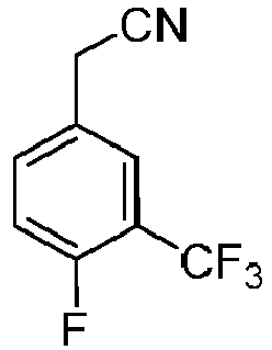
-4.43 A2 
-4.41 A3 
-4.45 A4 
-4.63 A5 
-4.73 A6 
-4.7 A7 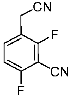
-4.73 A8 
-4.62 A9 
-5.14 A10 
-5.14 A11 
-4.85 A12 
-4.65 A13 
-4.95 A14 
-4.87 A15 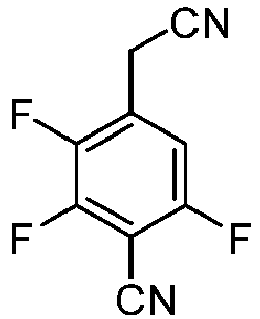
-5.14 A16 
-4.53 A17 
-4.78 A18 
-4.71 A19 
-5.02 A20 
-4.98 A21 
-5.16 A22 
-4.96 A23 
-4.24 A24 
-4.39 A25 
-4.31 A26 
-4.46 A27 
-4.85 A28 
-4.65 A29 
-5.26 A30 
-5.04 A31 
-5.12 A32 
-5.38 Table 2: Calculated LUMO levels of compounds of formula (I) wherein A1 and A2 may be selected the same or differently and A1 and A3 are not identical A1 A2 A3 Calculated LUMO [eV] A33 


-4.91 A34 


-4.71 A35 


-4.91 A36 


-4.71 A37 


-4.94 A38 


-4.93 A39 


-4.97 A40 


-5 A41 


-5.04 A42 


-4.88 A43 


-5.03 A44 


-5.06 A45 

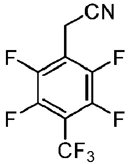
-4.87 A46 


-4.94 A47 


-5.03 A48 


-4.83 A49 


-4.86 A50 


-4.92 A51 


-4.65 A52 


-5.11 A53 


-5 A54 
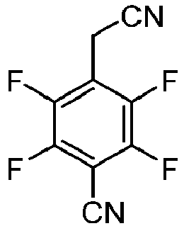

-5.17 A55 


-4.98 A56 


-5.16 A57 


-5.08 A58 


-4.88 A59 


-4.96 A60 


-5.01 A61 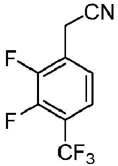

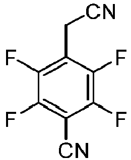
-4.83 A62 


-5.11 A63 


-5.03 A64 


-5.08 A65 


-4.98 A66 


-4.89 A67 


-4.98 A68 


-5.17 A69 


-4.98 A70 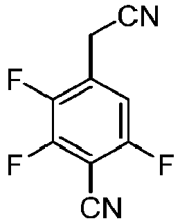


-5.16 A71 


-5.06 A72 


-4.97 A73 
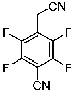

-5.05 A74 


-5.03 A75 


-5.13 A76 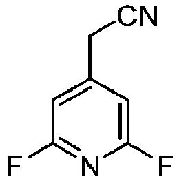


-5.09 A77 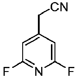


-5.08 A78 


-5.12 A79 


-4.93 A80 


-5.18 A81 


-4.99 A82 


-5.17 A83 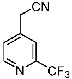


-5.11 A84 


-4.87 A85 


-4.92 A86 

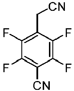
-4.89 A87 


-4.94 A88 


-5.08 A89 


-4.88 A90 


-5.01 A91 


-5.21 A92 


-5.02 A93 


-5.14 A94 


-5.24 A95 


-5.14 A96 
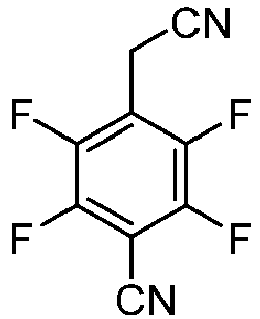

-5.17 A97 


-4.97 A98 


-5.14 A99 


-5.25 A100 


-5.06 A101 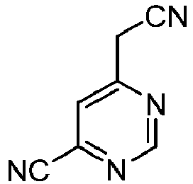


-5.32 - In Table 3 performance data for organic electroluminescent devices comprising a hole injection layer (HIL) comprising comparative and inventive compounds are shown:
Table 3: Organic electronic devices comprising an hole injection layer (HIL) comprising comparative and inventive compounds. U at 10 mA/cm2 [V] EQE at 10 mA/cm2 [%] LT at 30 mA/cm2 [h] C1 7.5 7 < 10 A5 3.9 8.9 85 A7 3.76 9.3 122 A11 3.74 9.4 129 A13 3.7 9.6 130 A14 3.73 9.5 125 A15 3.6 10.2 135 A19 3.8 9.8 128 A20 3.7 9.7 124 A29 3.5 10 123 A31 3.6 10.1 120 A33 3.8 10.4 140 A35 3.9 9.8 136 A37 4.1 9.6 127 A41 3.6 10.3 136 A47 3.7 10.5 145 A54 3.5 10.6 138 A64 3.6 9.4 120 A71 3.7 9.1 130 A75 3.5 8.9 125 A88 3.6 8.5 123 A94 3.5 9.7 132 A100 3.7 8.6 117 - As can be seen from Table 3, the operating voltage U for devices according to invention is lower than for the comparative compounds.
- As can be seen in Table 3, the external quantum efficiency EQE and lifetime LT for devices according to invention are increased compared to comparative compounds.
- A low operating voltage and/or high efficiency may be beneficial for reduced power consumption and improved battery life, in particular in mobile devices.
- A long lifetime is beneficial for long-time stability of devices.
- The particular combinations of elements and features in the above detailed embodiments are exemplary only; the interchanging and substitution of these teachings with other teachings in this and the patents/applications incorporated by reference are also expressly contemplated. As those skilled in the art will recognize, variations, modifications, and other implementations of what is described herein can occur to those of ordinary skill in the art without departing from the spirit and the scope of the invention as claimed. Accordingly, the foregoing description is by way of example only and is not intended as limiting. In the claims, the word "comprising" does not exclude other elements or steps, and the indefinite article "a" or "an" does not exclude a plurality. The mere fact that certain measures are recited in mutually different dependent claims does not indicate that a combination of these measured cannot be used to advantage. The invention's scope is defined in the following claims and the equivalents thereto. Furthermore, reference signs used in the description and claims do not limit the scope of the invention as claimed.
Claims (15)
- A compound of formula (I)
 whereby A1 is selected from formula (II)
 X1 is selected from CR1;X2 is selected from CR2 or N;X3 is selected from CR3 or N;X4 is selected from CR4 or N;X5 is selected from CR5 or N;R1 is selected from D or H,R2, R3, R4 and R5 (if present) are independently selected from CN, partially fluorinated or perfluorinated C1 to C8 alkyl, halogen, Cl, F, D or H, whereby when any of R2, R3, R4 and R5 is present, then the corresponding X2, X3, X4 and X5 is not N;with the proviso that either- at least one R2 to R5 is selected from selected from CN, partially fluorinated or perfluorinated C1 to Cs alkyl, halogen, Cl, F; or- at least one X2 to X5 is N;A2 and A3 are independently selected from formula (III)
 wherein Ar is independently selected from substituted or unsubstituted C6 to C18 aryl and substituted or unsubstituted C2 to C18 heteroaryl, wherein the substituents on Ar are independently selected from CN, partially or perfluorinated C1 to C6 alkyl, halogen, Cl, F, D; andR' is selected from Ar, substituted or unsubstituted C6 to C18 aryl or C3 to C18 heteroaryl, partially flurorinated or perfluorinated C1 to C8 alkyl, halogen, F or CN;and wherein the asterix "*" denotes the binding position.
 - The compound of Claim 1, selected of the formula (IV)


- The compound of Claim 1 or 2 whereby formula (II) does not include the following moieties:


- The compound of any of the Claims 1 to 3 whereby formula (III) does not include the following moieties:


- The compound of any of the claims 1 to 4, whereby A1 differs from A2 and/or A3.
- The compound of any of the claims 1 to 5, whereby X3 is selected from N or CR3, wherein R3 is selected from CN, partially flurorinated or perfluorinated C1 to C8 alkyl.
- The compound of any of the claims 1 to 6, whereby one of R2 and R3 is selected from CN, partially flurorinated or perfluorinated C1 to C8 alkyl and at least one R2 to R5 is independently selected from CN, partially flurorinated or perfluorinated C1 to Cs alkyl, halogen, Cl, F.
- The compound of any of the Claims 1 to 7, whereby R5 is D or H.
- The compound any of the claims 1 to 8, whereby at least two out of R2 to R5 are independently selected from halogen, Cl, F.
- An organic electronic device comprising an anode layer, a cathode layer, at least one photoactive layer and at least one organic semiconductor layer, wherein the at least one organic semiconductor layer is arranged between the at least one photoactive layer and the cathode; and wherein the at least one organic semiconductor layer comprises a compound of any of the claims 1 to 9.
- The organic electronic device of claim 10, whereby the organic semiconductor layer comprises a composition comprising a compound of formula (IV) and at least one compound of formula (IVa) to (IVd)


- The organic electronic device of claim 10 or 11, whereby the organic electronic device comprises at least one photoactive layer, wherein the at least one photoactive layer is arranged between the anode layer and the cathode layer and at least one of the at least one organic semiconductor layers is arranged between the anode layer and the at least one photoactive layer.
- The organic electronic device of any of the claims 10 to 12, whereby the organic electronic device comprises at least two photoactive layers, wherein at least one of the at least one organic semiconductor layers is arranged between the first and the second photoactive layer.
- The organic electronic device of any of the claims 10 to 13, whereby the electronic organic device is an electroluminescent device, preferably an organic light emitting diode.
- A display device comprising an organic electronic device according to any of the claims 10 to 14.
Priority Applications (81)
| Application Number | Priority Date | Filing Date | Title |
|---|---|---|---|
| EP20203457.5A EP3989303A1 (en) | 2020-10-22 | 2020-10-22 | Organic compound of formula (i) for use in organic electronic devices, an organic electronic device comprising a compound of formula (i) and a display device comprising the organic electronic device |
| EP21731517.5A EP4165694B1 (en) | 2020-06-12 | 2021-06-14 | Organic light emitting diode and device comprising the same |
| KR1020237001081A KR102950743B1 (en) | 2020-06-12 | 2021-06-14 | Organic light-emitting diode and device including the same |
| US18/000,910 US20230225201A1 (en) | 2020-06-12 | 2021-06-14 | Organic Light Emitting Diode and Device Comprising the Same |
| PCT/EP2021/065949 WO2021250279A1 (en) | 2020-06-12 | 2021-06-14 | Organic light emitting diode and device comprising the same |
| CN202180040710.5A CN115868257A (en) | 2020-06-12 | 2021-06-14 | Organic light emitting diode and device comprising the same |
| US18/002,562 US20230240132A1 (en) | 2020-06-22 | 2021-06-18 | Organic Electronic Device Comprising a Compound of Formula (1), Display Device Comprising the Organic Electronic Device as Well as Compounds of Formula (1) for Use in Organic Electronic Devices |
| KR1020237002132A KR20230028769A (en) | 2020-06-22 | 2021-06-18 | Compounds of formula (I) for use in organic electronic devices comprising compounds of formula (I), display devices comprising organic electronic devices and organic electronic devices |
| US18/002,158 US20230232712A1 (en) | 2020-06-22 | 2021-06-18 | Organic Electronic Device and Display Device Comprising the Organic Electronic Device as Well as a Composition for Use in Organic Electronic Devices |
| EP21733806.0A EP4169087B1 (en) | 2020-06-22 | 2021-06-18 | Organic electronic device and display device comprising the organic electronic device as well as a composition for use in organic electronic devices |
| US18/002,144 US20230225141A1 (en) | 2020-06-22 | 2021-06-18 | Organic Compound of Formula (I) for Use in Organic Electronic Devices, an Organic Electronic Device Comprising a Compound of Formula (I) and a Display Device Comprising the Organic Electronic Device |
| EP21733448.1A EP4168379B1 (en) | 2020-06-22 | 2021-06-18 | Organic compound of formula (i) for use in organic electronic devices, an organic electronic device comprising a compound of formula (i) and a display device comprising the organic electronic device |
| CN202180044197.7A CN115918299A (en) | 2020-06-22 | 2021-06-18 | Organic compounds of formula (I) for use in organic electronic devices, organic electronic devices comprising compounds of formula (I), and display devices comprising said organic electronic devices |
| EP21733811.0A EP4169092B1 (en) | 2020-06-22 | 2021-06-18 | Organic electronic device and display device comprising the organic electronic device as well as a composition for use in organic electronic devices |
| KR1020237002133A KR20230028770A (en) | 2020-06-22 | 2021-06-18 | Organic electronic devices, and display devices comprising organic electronic devices, and compositions for use in organic electronic devices |
| HUE21733806A HUE066882T2 (en) | 2020-06-22 | 2021-06-18 | Organic electronic device and display device comprising the organic electronic device as well as a composition for use in organic electronic devices |
| CN202180044230.6A CN116076169A (en) | 2020-06-22 | 2021-06-18 | Organic compounds of formula (I), compositions comprising compounds of formula (IV) and at least one compound of formulas (IVa) to (IVd), organic semiconductors comprising said compounds or compositions, for use in organic electronic devices layer, an organic electronic device comprising the organic semiconductor layer, and a display device comprising the organic electronic device |
| CN202180044546.5A CN115943758A (en) | 2020-06-22 | 2021-06-18 | Organic electronic devices comprising compounds of formula (I), display devices comprising said organic electronic devices, and compounds of formula (I) for organic electronic devices |
| KR1020237002135A KR20230028772A (en) | 2020-06-22 | 2021-06-18 | an organic semiconductor layer comprising an organic compound of formula (I), a composition comprising a compound of formula (IV) and at least one compound of formulas (IVa) to (IVd), or an organic semiconductor layer comprising a compound or composition, for use in an organic electronic device; and an organic electronic device including an organic semiconductor layer, and a display device including the organic electronic device. |
| EP21733449.9A EP4168380A2 (en) | 2020-06-22 | 2021-06-18 | Organic electronic device comprising a compound of formula (i), display device comprising the organic electronic device as well as compounds of formula (i) for use in organic electronic devices |
| HUE21733451A HUE068204T2 (en) | 2020-06-22 | 2021-06-18 | Organic compound of formula (i) for use in organic electronic devices, an organic electronic device comprising a compound of formula (i) and a display device comprising the organic electronic device |
| JP2022579680A JP2023531688A (en) | 2020-06-22 | 2021-06-18 | Organic compounds of formula (I) for use in organic electronic devices, compositions comprising a compound of formula (IV) and at least one of the compounds of formulae (IVa) to (IVd), organic semiconductor layers comprising said compounds or compositions, organic electronic devices comprising said organic semiconductor layers, and display devices comprising said organic electronic devices. |
| CN202180044505.6A CN115867531A (en) | 2020-06-22 | 2021-06-18 | Organic compound of formula (I) for organic electronic device, organic electronic device comprising compound of formula (I) and display device comprising said organic electronic device |
| TW110122344A TWI865790B (en) | 2020-06-22 | 2021-06-18 | Organic electronic device comprising a compound of formula (i), display device comprising the organic electronic device as well as compounds of formula (i) for use in organic electronic devices |
| TW110122435A TWI874671B (en) | 2020-06-22 | 2021-06-18 | ORGANIC COMPOUND OF FORMULA (I) FOR USE IN ORGANIC ELECTRONIC DEVICES, A COMPOSITION COMPRISING A COMPOUND OF FORMULA (IV) AND AT LEAST ONE COMPOUND OF FORMULA (IVa) TO (IVd), AN ORGANIC SEMICONDUCTOR LAYER COMPRISING THE COMPOUND OR COMPOSITION, AN ORGANIC ELECTRONIC DEVICE COMPRISING THE ORGANIC SEMICONDUCTOR LAYER, AND A DISPLAY DEVICE COMPRISING THE ORGANIC ELECTRONIC DEVICE |
| US18/002,604 US20230240138A1 (en) | 2020-06-22 | 2021-06-18 | Organic Electronic Device and Display Device Comprising the Organic Electronic Device as Well as a Composition for Use in Organic Electronic Devices |
| PCT/EP2021/066605 WO2021259788A1 (en) | 2020-06-22 | 2021-06-18 | Organic electronic device and display device comprising the organic electronic device as well as a composition for use in organic electronic devices |
| TW110122345A TWI865791B (en) | 2020-06-22 | 2021-06-18 | Organic electronic device and display device comprising the organic electronic device as well as a composition for use in organic electronic devices |
| KR1020237002120A KR102887494B1 (en) | 2020-06-22 | 2021-06-18 | An organic electronic device comprising a compound of formula (I), a display device comprising an organic electronic device, and a compound of formula (I) for use in an organic electronic device |
| KR1020237002123A KR20230027216A (en) | 2020-06-22 | 2021-06-18 | Organic compounds of formula (I) for use in organic electronic devices, organic electronic devices comprising the compounds of formula (I), and display devices comprising the organic electronic devices |
| TW110122341A TW202231625A (en) | 2020-06-22 | 2021-06-18 | Organic electronic device comprising a compound of formula (i), display device comprising the organic electronic device as well as compounds of formula (i) for use in organic electronic devices |
| PCT/EP2021/066612 WO2021259792A1 (en) | 2020-06-22 | 2021-06-18 | ORGANIC COMPOUND OF FORMULA (I) FOR USE IN ORGANIC ELECTRONIC DEVICES, A COMPOSITION COMPRISING A COMPOUND OF FORMULA (IV) AND AT LEAST ONE COMPOUND OF FORMULA (IVa) TO (IVd), AN ORGANIC SEMICONDUCTOR LAYER COMPRISING THE COMPOUND OR COMPOSITION, AN ORGANIC ELECTRONIC DEVICE COMPRISING THE ORGANIC SEMICONDUCTOR LAYER, AND A DISPLAY DEVICE COMPRISING THE ORGANIC ELECTRONIC DEVICE |
| KR1020237002122A KR20230028424A (en) | 2020-06-22 | 2021-06-18 | Organic compounds of formula (I) for use in organic electronic devices, organic electronic devices comprising the compounds of formula (I), and display devices comprising the organic electronic devices |
| EP21733807.8A EP4169088B1 (en) | 2020-06-22 | 2021-06-18 | Organic electronic device comprising a compound of formula (1), display device comprising the organic electronic device as well as compounds of formula (1) for use in organic electronic devices |
| EP21733809.4A EP4169090B1 (en) | 2020-06-22 | 2021-06-18 | Organic electronic device comprising a compound of formula (i), display device comprising the organic electronic device as well as compounds of formula (i) for use in organic electronic devices |
| CN202180044264.5A CN115918300A (en) | 2020-06-22 | 2021-06-18 | Organic electronic devices comprising compounds of formula (I), display devices comprising said organic electronic devices, and compounds of formula (I) used in organic electronic devices |
| PCT/EP2021/066597 WO2021259782A2 (en) | 2020-06-22 | 2021-06-18 | Organic compound of formula (i) for use in organic electronic devices, an organic electronic device comprising a compound of formula (i) and a display device comprising the organic electronic device |
| PCT/EP2021/066604 WO2021259787A1 (en) | 2020-06-22 | 2021-06-18 | Organic compound of formula (i) for use in organic electronic devices, an organic electronic device comprising a compound of formula (i) and a display device comprising the organic electronic device |
| CN202180044519.8A CN116584178A (en) | 2020-06-12 | 2021-06-18 | Organic compounds of formula (I), compositions comprising compounds of formula (IV) and at least one compound of formulas (IVa) to (IVd), organic semiconductors comprising said compounds or compositions, for use in organic electronic devices layer, an organic electronic device comprising the organic semiconductor layer, and a display device comprising the organic electronic device |
| US18/002,088 US20230232711A1 (en) | 2020-06-22 | 2021-06-18 | Organic Electronic Device Comprising a Compound of Formula (I), Display Device Comprising the Organic Electronic Device as Well as Compounds of Formula (I) for Use in Organic Electronic Devices |
| EP21733810.2A EP4169091A1 (en) | 2020-06-22 | 2021-06-18 | Organic compound of formula (i) for use in organic electronic devices, a composition comprising a compound of formula (iv) and at least one compound of formula (iva) to (ivd), an organic semiconductor layer comprising the compound or composition, an organic electronic device comprising the organic semiconductor layer, and a display device comprising the organic electronic device |
| JP2022579039A JP7844359B2 (en) | 2020-06-22 | 2021-06-18 | Organic electronic devices, display devices including organic electronic devices, and compositions for use in organic electronic devices. |
| KR1020237002138A KR102919031B1 (en) | 2020-06-22 | 2021-06-18 | An organic electronic device comprising a compound of formula (1), a display device comprising an organic electronic device, and a compound of formula (1) for use in an organic electronic device |
| US18/002,008 US20230247901A1 (en) | 2020-06-22 | 2021-06-18 | Organic Electronic Device Comprising a Compound of Formula (I), Display Device Comprising the Organic Electronic Device as Well as Compounds of Formula (I) for Use in Organic Electronic Devices |
| TW110122281A TWI870601B (en) | 2020-06-22 | 2021-06-18 | Organic electronic device and display device comprising the organic electronic device as well as a composition for use in organic electronic devices |
| PCT/EP2021/066603 WO2021259786A1 (en) | 2020-06-22 | 2021-06-18 | Organic compound of formula (i) for use in organic electronic devices, an organic electronic device comprising a compound of formula (i) and a display device comprising the organic electronic device |
| PCT/EP2021/066601 WO2021259784A2 (en) | 2020-06-22 | 2021-06-18 | Organic electronic device comprising a compound of formula (i), display device comprising the organic electronic device as well as compounds of formula (i) for use in organic electronic devices |
| US18/002,013 US20230240137A1 (en) | 2020-06-22 | 2021-06-18 | Organic Electronic Device Comprising a Compound of Formula (I), Display Device Comprising the Organic Electronic Device as Well as Compounds of Formula (I) for Use in Organic Electronic Devices |
| JP2022579037A JP7842040B2 (en) | 2020-06-22 | 2021-06-18 | Organic compound of formula (I) for use in organic electronic devices, organic electronic device containing compound of formula (I), and display device containing organic electronic device. |
| KR1020237002134A KR20230028771A (en) | 2020-06-22 | 2021-06-18 | Organic compounds of formula (I) for use in organic electronic devices, organic electronic devices comprising the compounds of formula (I), and display devices comprising the organic electronic devices |
| TW110122340A TWI906315B (en) | 2020-06-22 | 2021-06-18 | Organic compound of formula (i) for use in organic electronic devices, an organic electronic device comprising a compound of formula (i) and a display device comprising the organic electronic device |
| KR1020237002140A KR20230028774A (en) | 2020-06-22 | 2021-06-18 | Organic electronic devices, and display devices comprising organic electronic devices, and compositions for use in organic electronic devices |
| PCT/EP2021/066606 WO2021259789A1 (en) | 2020-06-22 | 2021-06-18 | Organic electronic device comprising a compound of formula (1), display device comprising the organic electronic device as well as compounds of formula (1) for use in organic electronic devices |
| PCT/EP2021/066602 WO2021259785A1 (en) | 2020-06-22 | 2021-06-18 | Organic electronic device comprising a compound of formula (i), display device comprising the organic electronic device as well as compounds of formula (i) for use in organic electronic devices |
| TW110122342A TW202231624A (en) | 2020-06-22 | 2021-06-18 | Organic electronic device comprising a compound of formula (i), display device comprising the organic electronic device as well as compounds of formula (i) for use in organic electronic devices |
| PCT/EP2021/066613 WO2021259793A1 (en) | 2020-06-22 | 2021-06-18 | Organic electronic device and display device comprising the organic electronic device as well as a composition for use in organic electronic devices |
| KR1020237002139A KR20230028427A (en) | 2020-06-22 | 2021-06-18 | an organic semiconductor layer comprising an organic compound of formula (I), a composition comprising a compound of formula (IV) and at least one compound of formulas (IVa) to (IVd), or an organic semiconductor layer comprising a compound or composition, for use in an organic electronic device; and an organic electronic device including an organic semiconductor layer, and a display device including the organic electronic device. |
| TW110122434A TWI881141B (en) | 2020-06-22 | 2021-06-18 | ORGANIC COMPOUND OF FORMULA (I) FOR USE IN ORGANIC ELECTRONIC DEVICES, A COMPOSITION COMPRISING A COMPOUND OF FORMULA (IV) AND AT LEAST ONE COMPOUND OF FORMULA (IVa) TO (IVd), AN ORGANIC SEMICONDUCTOR LAYER COMPRISING THE COMPOUND OR COMPOSITION, AN ORGANIC ELECTRONIC DEVICE COMPRISING THE ORGANIC SEMICONDUCTOR LAYER, AND A DISPLAY DEVICE COMPRISING THE ORGANIC ELECTRONIC DEVICE |
| EP21733452.3A EP4169086B1 (en) | 2020-06-22 | 2021-06-18 | Organic compound of formula (i) for use in organic electronic devices, an organic electronic device comprising a compound of formula (i) and a display device comprising the organic electronic device |
| CN202180044582.1A CN115943759A (en) | 2020-06-22 | 2021-06-18 | Organic electronic device comprising compound of formula (1), display device comprising said organic electronic device, and compound of formula (1) used in organic electronic device |
| US18/002,609 US20230240139A1 (en) | 2020-06-22 | 2021-06-18 | Organic Compound of Formula (I) for Use in Organic Electronic Devices, a Composition Comprising a Compound of Formula (IV) and at Least One Compound of Formula (IVa) to (IVd), an Organic Semiconductor Layer Comprising the Compound or Composition, an Organic Electronic Device Comprising the Organic Semiconductor Layer, and a Display Device Comprising the Organic Electronic Device |
| TW110122298A TWI891817B (en) | 2020-06-22 | 2021-06-18 | Organic compound of formula (i) for use in organic electronic devices, an organic electronic device comprising a compound of formula (i) and a display device comprising the organic electronic device |
| EP21733808.6A EP4169089A1 (en) | 2020-06-22 | 2021-06-18 | Organic compound of formula (i) for use in organic electronic devices, a composition comprising a compound of formula (iv) and at least one compound of formula (iva) to (ivd), an organic semiconductor layer comprising the compound or composition, an organic electronic device comprising the organic semiconductor layer, and a display device comprising the organic electronic device |
| US18/002,172 US20230227401A1 (en) | 2020-06-22 | 2021-06-18 | Organic Compound of Formula (I) for Use in Organic Electronic Devices, a Composition Comprising a Compound of Formula (IV) and at Least One Compound of Formula (IVa) to (IVd), an Organic Semiconductor Layer Comprising the Compound or Composition, an Organic Electronic Device Comprising the Organic Semiconductor Layer, and a Display Device Comprising the Organic Electronic Device |
| US18/002,003 US20230247900A1 (en) | 2020-06-22 | 2021-06-18 | Organic Compound of Formula (I) for Use in Organic Electronic Devices, an Organic Electronic Device Comprising a Compound of Formula (I) and a Display Device Comprising the Organic Electronic Device |
| CN202180044543.1A CN115943757A (en) | 2020-06-22 | 2021-06-18 | Organic electronic devices comprising compounds of formula (I), display devices comprising said organic electronic devices, and compounds of formula (I) used in organic electronic devices |
| JP2022579682A JP7771107B2 (en) | 2020-06-22 | 2021-06-18 | Organic electronic device and display device including said organic electronic device, and composition for use in organic electronic device |
| EP21733451.5A EP4169085B1 (en) | 2020-06-22 | 2021-06-18 | Organic compound of formula (i) for use in organic electronic devices, an organic electronic device comprising a compound of formula (i) and a display device comprising the organic electronic device |
| CN202180044534.2A CN116058109B (en) | 2020-06-22 | 2021-06-18 | Organic electronic devices and display devices comprising said organic electronic devices, as well as compositions for organic electronic devices. |
| HUE21733811A HUE067638T2 (en) | 2020-06-22 | 2021-06-18 | An organic electronic device and a display device containing an organic electronic device, as well as a composition that can be used in an organic electronic device |
| PCT/EP2021/066610 WO2021259791A1 (en) | 2020-06-22 | 2021-06-18 | Organic electronic device comprising a compound of formula (i), display device comprising the organic electronic device as well as compounds of formula (i) for use in organic electronic devices |
| JP2022579040A JP2023530520A (en) | 2020-06-22 | 2021-06-18 | Organic compounds of formula (I) for use in organic electronic devices, compositions comprising a compound of formula (IV) and at least one compound of formula (IVa) to (IVd), organic semiconductor layers comprising said compounds or compositions, organic electronic devices comprising said organic semiconductor layers, and display devices comprising said organic electronic devices. |
| EP26160825.1A EP4729512A2 (en) | 2020-06-22 | 2021-06-18 | Organic compound of formula (i) for use in organic electronic devices, an organic electronic device comprising a compound of formula (i) and a display device comprising the organic electronic device |
| KR1020237002121A KR20230028768A (en) | 2020-06-22 | 2021-06-18 | Organic electronic devices comprising compounds of formula (I), organic electronic devices and display devices comprising compounds of formula (I) for use in organic electronic devices |
| CN202180044232.5A CN115885598A (en) | 2020-06-22 | 2021-06-18 | Organic compounds of formula (I) for use in organic electronic devices, organic electronic devices comprising compounds of formula (I) and display devices comprising said organic electronic devices |
| TW110122294A TWI890813B (en) | 2020-06-22 | 2021-06-18 | Organic compound of formula (i) for use in organic electronic devices, an organic electronic device comprising a compound of formula (i) and a display device comprising the organic electronic device |
| US18/002,082 US20230232710A1 (en) | 2020-06-22 | 2021-06-18 | Organic Compound of Formula (I) for Use in Organic Electronic Devices, an Organic Electronic Device Comprising a Compound of Formula (I) and a Display Device Comprising the Organic Electronic Device |
| PCT/EP2021/066607 WO2021259790A1 (en) | 2020-06-22 | 2021-06-18 | Organic compound of formula (i) for use in organic electronic devices, a composition comprising a compound of formula (iv) and at least one compound of formula (iva) to (ivd), an organic semiconductor layer comprising the compound or composition, an organic electronic device comprising the organic semiconductor layer, and a display device comprising the organic electronic device |
| TW110122346A TWI876063B (en) | 2020-06-22 | 2021-06-18 | Organic electronic device comprising a compound of formula (i), display device comprising the organic electronic device as well as compounds of formula (i) for use in organic electronic devices |
| CN202180045206.4A CN115804267B (en) | 2020-06-22 | 2021-06-18 | Organic electronic device and display device comprising the same and composition for organic electronic device |
| EP21733450.7A EP4169084B1 (en) | 2020-06-22 | 2021-06-18 | Organic electronic device comprising a compound of formula (i), display device comprising the organic electronic device |
Applications Claiming Priority (1)
| Application Number | Priority Date | Filing Date | Title |
|---|---|---|---|
| EP20203457.5A EP3989303A1 (en) | 2020-10-22 | 2020-10-22 | Organic compound of formula (i) for use in organic electronic devices, an organic electronic device comprising a compound of formula (i) and a display device comprising the organic electronic device |
Publications (1)
| Publication Number | Publication Date |
|---|---|
| EP3989303A1 true EP3989303A1 (en) | 2022-04-27 |
Family
ID=73013320
Family Applications (1)
| Application Number | Title | Priority Date | Filing Date |
|---|---|---|---|
| EP20203457.5A Pending EP3989303A1 (en) | 2020-06-12 | 2020-10-22 | Organic compound of formula (i) for use in organic electronic devices, an organic electronic device comprising a compound of formula (i) and a display device comprising the organic electronic device |
Country Status (1)
| Country | Link |
|---|---|
| EP (1) | EP3989303A1 (en) |
Citations (11)
| Publication number | Priority date | Publication date | Assignee | Title |
|---|---|---|---|---|
| EP1988587A1 (en) * | 2007-04-30 | 2008-11-05 | Novaled AG | Oxocarbon, pseudo oxocarbon and radialene compounds and their use |
| EP2180029A1 (en) | 2008-10-23 | 2010-04-28 | Novaled AG | Radialene compounds and their use |
| EP2722908A1 (en) | 2012-10-17 | 2014-04-23 | Novaled AG | Phosphorescent OLED and hole transporting materials for phosphorescent OLEDs |
| WO2016097017A1 (en) | 2014-12-16 | 2016-06-23 | Novaled Gmbh | Substituted 1,2,3-triylidenetris(cyanomethanylylidene)) cyclopropanes for vte, electronic devices and semiconducting materials using them |
| US20180166509A1 (en) * | 2017-07-28 | 2018-06-14 | Shanghai Tianma AM-OLED Co., Ltd. | Organic light-emitting diode, display panel and display device |
| WO2019168368A1 (en) * | 2018-02-28 | 2019-09-06 | 주식회사 엘지화학 | Organic light emitting diode |
| EP3799143A1 (en) * | 2019-09-26 | 2021-03-31 | Novaled GmbH | First and second organic semiconductor layer and organic electronic device comprising the same |
| EP3930024A1 (en) * | 2020-06-22 | 2021-12-29 | Novaled GmbH | Organic electronic device and display device comprising the organic electronic device as well as a composition for use in organic electronic devices |
| EP3930022A1 (en) * | 2020-06-22 | 2021-12-29 | Novaled GmbH | Organic electronic device and display device comprising the organic electronic device as well as a composition for use in organic electronic devices |
| EP4165694A1 (en) * | 2020-06-12 | 2023-04-19 | Novaled GmbH | Organic light emitting diode and device comprising the same |
| EP4169085A1 (en) * | 2020-06-22 | 2023-04-26 | Novaled GmbH | Organic compound of formula (i) for use in organic electronic devices, an organic electronic device comprising a compound of formula (i) and a display device comprising the organic electronic device |
-
2020
- 2020-10-22 EP EP20203457.5A patent/EP3989303A1/en active Pending
Patent Citations (11)
| Publication number | Priority date | Publication date | Assignee | Title |
|---|---|---|---|---|
| EP1988587A1 (en) * | 2007-04-30 | 2008-11-05 | Novaled AG | Oxocarbon, pseudo oxocarbon and radialene compounds and their use |
| EP2180029A1 (en) | 2008-10-23 | 2010-04-28 | Novaled AG | Radialene compounds and their use |
| EP2722908A1 (en) | 2012-10-17 | 2014-04-23 | Novaled AG | Phosphorescent OLED and hole transporting materials for phosphorescent OLEDs |
| WO2016097017A1 (en) | 2014-12-16 | 2016-06-23 | Novaled Gmbh | Substituted 1,2,3-triylidenetris(cyanomethanylylidene)) cyclopropanes for vte, electronic devices and semiconducting materials using them |
| US20180166509A1 (en) * | 2017-07-28 | 2018-06-14 | Shanghai Tianma AM-OLED Co., Ltd. | Organic light-emitting diode, display panel and display device |
| WO2019168368A1 (en) * | 2018-02-28 | 2019-09-06 | 주식회사 엘지화학 | Organic light emitting diode |
| EP3799143A1 (en) * | 2019-09-26 | 2021-03-31 | Novaled GmbH | First and second organic semiconductor layer and organic electronic device comprising the same |
| EP4165694A1 (en) * | 2020-06-12 | 2023-04-19 | Novaled GmbH | Organic light emitting diode and device comprising the same |
| EP3930024A1 (en) * | 2020-06-22 | 2021-12-29 | Novaled GmbH | Organic electronic device and display device comprising the organic electronic device as well as a composition for use in organic electronic devices |
| EP3930022A1 (en) * | 2020-06-22 | 2021-12-29 | Novaled GmbH | Organic electronic device and display device comprising the organic electronic device as well as a composition for use in organic electronic devices |
| EP4169085A1 (en) * | 2020-06-22 | 2023-04-26 | Novaled GmbH | Organic compound of formula (i) for use in organic electronic devices, an organic electronic device comprising a compound of formula (i) and a display device comprising the organic electronic device |
Non-Patent Citations (1)
| Title |
|---|
| YASUHIKO SHIROTAHIROSHI KAGEYAMA, CHEM. REV., vol. 107, 2007, pages 953 - 1010 |
Similar Documents
| Publication | Publication Date | Title |
|---|---|---|
| EP3989305B1 (en) | Organic electronic device comprising a compound of formula (i), and display device comprising the organic electronic device. | |
| EP4168379B1 (en) | Organic compound of formula (i) for use in organic electronic devices, an organic electronic device comprising a compound of formula (i) and a display device comprising the organic electronic device | |
| EP4284780B1 (en) | Organic compound of formula (i) for use in organic electronic devices, an organic electronic device comprising a compound of formula (i) and a display device comprising the organic electronic device | |
| KR102726233B1 (en) | Active OLED display | |
| EP3989302B1 (en) | Organic compound of formula (i) for use in organic electronic devices, an organic electronic device comprising a compound of formula (i) and a display device comprising the organic electronic device | |
| EP3930023B1 (en) | Organic electronic device comprising a compound of formula (1), display device comprising the organic electronic device as well as compounds of formula (1) for use in organic electronic devices | |
| EP4155303A1 (en) | Organic compound of formula (i) for use in organic electronic devices, a composition comprising a compound of formula (iv) and at least one compound of formula (iva) to (ivd), an organic semiconductor layer comprising the compound or composition, an organic electronic device comprising the organic semiconductor layer, and a display device comprising the organic electronic device | |
| EP3989304A1 (en) | Organic compound of formula (i) for use in organic electronic devices, an organic electronic device comprising a compound of formula (i) and a display device comprising the organic electronic device |
Legal Events
| Date | Code | Title | Description |
|---|---|---|---|
| PUAI | Public reference made under article 153(3) epc to a published international application that has entered the european phase |
Free format text: ORIGINAL CODE: 0009012 |
|
| STAA | Information on the status of an ep patent application or granted ep patent |
Free format text: STATUS: THE APPLICATION HAS BEEN PUBLISHED |
|
| AK | Designated contracting states |
Kind code of ref document: A1 Designated state(s): AL AT BE BG CH CY CZ DE DK EE ES FI FR GB GR HR HU IE IS IT LI LT LU LV MC MK MT NL NO PL PT RO RS SE SI SK SM TR |
|
| STAA | Information on the status of an ep patent application or granted ep patent |
Free format text: STATUS: REQUEST FOR EXAMINATION WAS MADE |
|
| 17P | Request for examination filed |
Effective date: 20221013 |
|
| RBV | Designated contracting states (corrected) |
Designated state(s): AL AT BE BG CH CY CZ DE DK EE ES FI FR GB GR HR HU IE IS IT LI LT LU LV MC MK MT NL NO PL PT RO RS SE SI SK SM TR |
|
| STAA | Information on the status of an ep patent application or granted ep patent |
Free format text: STATUS: EXAMINATION IS IN PROGRESS |
|
| 17Q | First examination report despatched |
Effective date: 20231220 |