EP3989293A1 - Semiconductor device and manufacturing method therefor - Google Patents
Semiconductor device and manufacturing method therefor Download PDFInfo
- Publication number
- EP3989293A1 EP3989293A1 EP21773266.8A EP21773266A EP3989293A1 EP 3989293 A1 EP3989293 A1 EP 3989293A1 EP 21773266 A EP21773266 A EP 21773266A EP 3989293 A1 EP3989293 A1 EP 3989293A1
- Authority
- EP
- European Patent Office
- Prior art keywords
- semiconductor structure
- conductive layer
- substrate
- energy level
- fermi energy
- Prior art date
- Legal status (The legal status is an assumption and is not a legal conclusion. Google has not performed a legal analysis and makes no representation as to the accuracy of the status listed.)
- Granted
Links
Images


Classifications
-
- H—ELECTRICITY
- H10—SEMICONDUCTOR DEVICES; ELECTRIC SOLID-STATE DEVICES NOT OTHERWISE PROVIDED FOR
- H10D—INORGANIC ELECTRIC SEMICONDUCTOR DEVICES
- H10D8/00—Diodes
- H10D8/422—PN diodes having the PN junctions in mesas
-
- H—ELECTRICITY
- H10—SEMICONDUCTOR DEVICES; ELECTRIC SOLID-STATE DEVICES NOT OTHERWISE PROVIDED FOR
- H10D—INORGANIC ELECTRIC SEMICONDUCTOR DEVICES
- H10D12/00—Bipolar devices controlled by the field effect, e.g. insulated-gate bipolar transistors [IGBT]
- H10D12/211—Gated diodes
-
- H—ELECTRICITY
- H10—SEMICONDUCTOR DEVICES; ELECTRIC SOLID-STATE DEVICES NOT OTHERWISE PROVIDED FOR
- H10D—INORGANIC ELECTRIC SEMICONDUCTOR DEVICES
- H10D8/00—Diodes
- H10D8/411—PN diodes having planar bodies
-
- H—ELECTRICITY
- H10—SEMICONDUCTOR DEVICES; ELECTRIC SOLID-STATE DEVICES NOT OTHERWISE PROVIDED FOR
- H10D—INORGANIC ELECTRIC SEMICONDUCTOR DEVICES
- H10D12/00—Bipolar devices controlled by the field effect, e.g. insulated-gate bipolar transistors [IGBT]
- H10D12/01—Manufacture or treatment
- H10D12/021—Manufacture or treatment of gated diodes, e.g. field-controlled diodes [FCD]
-
- H—ELECTRICITY
- H10—SEMICONDUCTOR DEVICES; ELECTRIC SOLID-STATE DEVICES NOT OTHERWISE PROVIDED FOR
- H10D—INORGANIC ELECTRIC SEMICONDUCTOR DEVICES
- H10D30/00—Field-effect transistors [FET]
- H10D30/60—Insulated-gate field-effect transistors [IGFET]
- H10D30/67—Thin-film transistors [TFT]
- H10D30/6729—Thin-film transistors [TFT] characterised by the electrodes
- H10D30/6737—Thin-film transistors [TFT] characterised by the electrodes characterised by the electrode materials
- H10D30/6739—Conductor-insulator-semiconductor electrodes
-
- H—ELECTRICITY
- H10—SEMICONDUCTOR DEVICES; ELECTRIC SOLID-STATE DEVICES NOT OTHERWISE PROVIDED FOR
- H10D—INORGANIC ELECTRIC SEMICONDUCTOR DEVICES
- H10D64/00—Electrodes of devices having potential barriers
- H10D64/111—Field plates
-
- H—ELECTRICITY
- H10—SEMICONDUCTOR DEVICES; ELECTRIC SOLID-STATE DEVICES NOT OTHERWISE PROVIDED FOR
- H10D—INORGANIC ELECTRIC SEMICONDUCTOR DEVICES
- H10D64/00—Electrodes of devices having potential barriers
- H10D64/60—Electrodes characterised by their materials
- H10D64/66—Electrodes having a conductor capacitively coupled to a semiconductor by an insulator, e.g. MIS electrodes
- H10D64/661—Electrodes having a conductor capacitively coupled to a semiconductor by an insulator, e.g. MIS electrodes the conductor comprising a layer of silicon contacting the insulator, e.g. polysilicon having vertical doping variation
-
- H—ELECTRICITY
- H10—SEMICONDUCTOR DEVICES; ELECTRIC SOLID-STATE DEVICES NOT OTHERWISE PROVIDED FOR
- H10D—INORGANIC ELECTRIC SEMICONDUCTOR DEVICES
- H10D64/00—Electrodes of devices having potential barriers
- H10D64/60—Electrodes characterised by their materials
- H10D64/66—Electrodes having a conductor capacitively coupled to a semiconductor by an insulator, e.g. MIS electrodes
- H10D64/671—Electrodes having a conductor capacitively coupled to a semiconductor by an insulator, e.g. MIS electrodes the conductor having lateral variation in doping or structure
-
- H—ELECTRICITY
- H10—SEMICONDUCTOR DEVICES; ELECTRIC SOLID-STATE DEVICES NOT OTHERWISE PROVIDED FOR
- H10D—INORGANIC ELECTRIC SEMICONDUCTOR DEVICES
- H10D8/00—Diodes
-
- H—ELECTRICITY
- H10—SEMICONDUCTOR DEVICES; ELECTRIC SOLID-STATE DEVICES NOT OTHERWISE PROVIDED FOR
- H10D—INORGANIC ELECTRIC SEMICONDUCTOR DEVICES
- H10D8/00—Diodes
- H10D8/01—Manufacture or treatment
- H10D8/043—Manufacture or treatment of planar diodes
-
- H—ELECTRICITY
- H10—SEMICONDUCTOR DEVICES; ELECTRIC SOLID-STATE DEVICES NOT OTHERWISE PROVIDED FOR
- H10D—INORGANIC ELECTRIC SEMICONDUCTOR DEVICES
- H10D8/00—Diodes
- H10D8/01—Manufacture or treatment
- H10D8/045—Manufacture or treatment of PN junction diodes
Definitions
- the present disclosure relates to the field of semiconductor technologies, and more particularly, to a semiconductor device and a fabrication method thereof.
- a PN junction of the diode is designed as an abrupt junction, such that the total electric current of the diode is increased by increasing an electric current density of the diode under the same voltage.
- the diode provided with the abrupt junction has a small reverse breakdown voltage and a larger reverse current.
- An objective of the present disclosure is to provide a semiconductor device and a fabrication method thereof.
- the semiconductor device can increase the electric current density of its PN junction under the same voltage.
- a semiconductor device includes a substrate, a semiconductor structure, an insulating layer, and a conductive layer.
- the semiconductor structure is positioned on a side of the substrate and includes a first semiconductor structure and a second semiconductor structure, wherein the first semiconductor structure and the second semiconductor structure form a PN junction.
- the insulating layer is positioned on a side of the semiconductor structure facing away from the substrate.
- the conductive layer is positioned on a side of the insulating layer facing away from the substrate, and an orthographic projection of the conductive layer on the substrate at least partially overlaps an orthographic projection of the PN junction on the substrate.
- the conductive layer is configured to reduce a potential barrier of the PN junction formed by the first semiconductor structure and the second semiconductor structure.
- a method for fabricating a semiconductor device including:
- the present disclosure provides a semiconductor device and a fabrication method thereof.
- the semiconductor device includes a substrate, a semiconductor structure, an insulating layer, and a conductive layer.
- the semiconductor structure is positioned on a side of the substrate and includes a first semiconductor structure and a second semiconductor structure, wherein the first semiconductor structure and the second semiconductor structure form a PN junction.
- the insulating layer is positioned on a side of the semiconductor structure facing away from the substrate.
- the conductive layer is positioned on a side of the insulating layer facing away from the substrate, and an orthographic projection of the conductive layer on the substrate at least partially overlaps an orthographic projection of the PN junction on the substrate.
- the semiconductor device can increase the electric current density of the PN junction under the same voltage.
- the semiconductor device can affect the Fermi energy levels of the first semiconductor structure and the second semiconductor structure through the conductive layer, so that the Fermi energy levels of a part of the first semiconductor structure and a part of the second semiconductor structure positioned at the PN junction tend to be the same. In this way, the potential barrier of the PN junction is reduced, and the electric current density of the PN junction under the same voltage is increased.
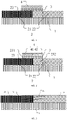
- FIG. 1 a schematic structural diagram of the semiconductor device according to an exemplary embodiment of the present disclosure is illustrated.
- the semiconductor device includes: a substrate 1, a semiconductor structure 2, an insulating layer 3, and a conductive layer 4.
- the semiconductor structure 2 is positioned on a side of the substrate 1 and includes a first semiconductor structure 21 and a second semiconductor structure 22, wherein the first semiconductor structure 21 and the second semiconductor structure 22 form a PN junction 23.
- the insulating layer 3 is positioned on a side of the semiconductor structure 2 facing away from the substrate 1.
- the conductive layer 4 is positioned on a side of the insulating layer 3 facing away from the substrate 1, and an orthographic projection of the conductive layer 4 on the substrate 1 at least partially overlaps an orthographic projection of the PN junction 23 on the substrate 1.
- the conductive layer is configured to reduce a potential barrier of the PN junction formed by the first semiconductor structure and the second semiconductor structure.
- the conductive layer 4 may act on a part of the semiconductor structure that overlaps the orthographic projection of the conductive layer 4 on the substrate 1, to change a Fermi energy level of this part of the semiconductor structure.
- the conductive layer can pull up the Fermi energy level of the semiconductor structure.
- the conductive layer can pull down the Fermi energy level of the semiconductor structure.
- the orthographic projection of the conductive layer 4 on the substrate 1 at least partially overlaps the orthographic projection of the PN junction 23 on the substrate 1.
- the conductive layer 4 can change the Fermi energy level(s) of the first semiconductor structure 21 and/or the second semiconductor structure 22, such that a differential between initial Fermi energy levels of a part of the first semiconductor structure 21 and of a part of the second semiconductor structure 22 positioned at the PN junction may be reduced by designing Fermi energy levels for different locations of the conductive layer. In this way, the potential barrier of the PN junction is reduced, and an electric current density of the semiconductor structure under the same voltage is increased.
- the initial Fermi energy levels of a part of the first semiconductor structure and of a part of the second semiconductor structure positioned at the PN junction refer to the Fermi energy levels, when the PN junction is not formed, of the part of the first semiconductor structure and of the part of the second semiconductor structure positioned at the PN junction.
- the conductive layer 4 may include a first conductive layer 41 and a second conductive layer 42.
- An orthographic projection of the first conductive layer 41 on the substrate 1 may be positioned on an orthographic projection of the first semiconductor structure 21 on the substrate 1, and the orthographic projection of the first conductive layer 41 on the substrate 1 may at least partially overlap the orthographic projection of the PN junction 23 on the substrate 1.
- An orthographic projection of the second conductive layer 42 on the substrate 1 may be positioned on an orthographic projection of the second semiconductor structure 22 on the substrate 1, and the orthographic projection of the second conductive layer 42 on the substrate 1 may at least partially overlap the orthographic projection of the PN junction 23 on the substrate 1.
- the PN junction 23 may include a first structure portion 231 positioned in the first semiconductor structure 21 and a second structure portion 232 positioned in the second semiconductor structure 22.
- the orthographic projection of the first conductive layer 41 on the substrate 1 may overlay the orthographic projection of the first structure portion 231 on the substrate 1.
- the orthographic projection of the second conductive layer 42 on the substrate 1 may overlay the orthographic projection of the second structure portion 232 on the substrate 1. As shown in FIG.
- the Fermi energy level of a material of the first semiconductor structure 21 when the Fermi energy level of a material of the first semiconductor structure 21 is greater than the Fermi energy level of a material of the second semiconductor structure 22, the Fermi energy level of a material of the first conductive layer 41 may be less than the Fermi energy level of the material of the first semiconductor structure 21, and the Fermi energy level of the material of the second conductive layer 42 may be greater than the Fermi energy level of the material of the second semiconductor structure.
- the material of the first semiconductor structure 21 may be an N-type semiconductor
- the material of the second semiconductor structure 22 may be a P-type semiconductor.
- the first conductive layer 41 may be a polysilicon conductor doped with P-type ions
- the second conductive layer 42 may be a polysilicon conductor doped with N-type ions.
- the first conductive layer 41 can pull down the Fermi energy level of the first structure portion 231 because the Fermi energy level of the material of the first conductive layer 41 is less than the Fermi energy level of the material of the first semiconductor structure 21.
- the second conductive layer 42 can pull up the Fermi energy level of the second structure portion 232 because the Fermi energy level of the material of the second conductive layer 42 is greater than the Fermi energy level of the material of the second semiconductor structure.
- FIG. 3 is a schematic structural diagram of a semiconductor device in the existing technologies
- FIG. 4 is a schematic structural diagram of the semiconductor device according to still another exemplary embodiment of the present disclosure.
- the semiconductor device includes a substrate 1, a first semiconductor structure 21, and a second semiconductor structure 22.
- the first semiconductor structure 21 may be an N-type semiconductor
- the second semiconductor structure may be a P-type semiconductor.
- FIG. 3 illustrates an energy band diagram of the PN junction 23.
- the PN junction in the existing technologies has a potential barrier h1.
- the first semiconductor structure 21 may also be an N-type semiconductor
- the second semiconductor structure 22 may also be a P-type semiconductor.
- FIG. 4 also illustrates an energy band diagram of the PN junction in the semiconductor structure of the present disclosure.
- the PN junction in the present disclosure has a potential barrier h2, and apparently, h2 is smaller than h1.
- the first semiconductor structure 21 may also be a P-type semiconductor
- the second semiconductor structure 22 may also be an N-type semiconductor
- the first conductive layer may be a polysilicon conductor doped with the N-type ions
- the second conductive layer may be a polysilicon conductor doped with the P-type ions.
- the Fermi energy level of the material of the first conductive layer 41 also may be equal to the Fermi energy level of the material of the second conductive layer 42, as long as the Fermi energy level of the material of the first conductive layer 41 and the Fermi energy level of the material of the second conductive layer 42 both are between the Fermi energy level of the material of the first semiconductor structure 21 and the Fermi energy level of the material of the second semiconductor structure 22. In this way, the effect of reducing the differential between the Fermi energy level of the first semiconductor structure 21 and the Fermi energy level of the second semiconductor structure 22 can be implemented.
- the Fermi energy level of the material of the first conductive layer 41 and the Fermi energy level of the material of the second conductive layer 42 may also both be greater than or less than the Fermi energy level of the material of the first semiconductor structure 21 and the Fermi energy level of the material of the second semiconductor structure 22.
- the first semiconductor structure is an N-type semiconductor and the second semiconductor structure is a P-type semiconductor. That is, the Fermi energy level of the material of the first semiconductor structure is greater than the Fermi energy level of the material of the second semiconductor structure.
- the Fermi energy level of the material of the first conductive layer 41 and the Fermi energy level of the material of the second conductive layer 42 both are greater than the Fermi energy level of the material of the first semiconductor structure and the Fermi energy level of the material of the second semiconductor structure, and when the differential obtained by subtracting the Fermi energy level of the material of the first semiconductor structure 21 from the Fermi energy level of the material of the first conductive layer 41 is less than the differential obtained by subtracting the Fermi energy level of the material of the second semiconductor structure 22 from the Fermi energy level of the material of the second conductive layer 42, a degree of pulling up the Fermi energy level of the first semiconductor structure 21 by the first conductive layer 41 is less than a degree of pulling up the Fermi energy level of the second semiconductor structure 22 by the second conductive layer 42.
- the differential between the Fermi energy level of the first semiconductor structure 21 and the Fermi energy level of the second semiconductor structure 22 still can be reduced, and thus the potential barrier of the PN junction is reduced, and the electric current density of the PN junction under the same voltage is increased.
- the Fermi energy level of the first conductive layer 41 and the Fermi energy level of the second conductive layer 42 both are less than the Fermi energy level of the first semiconductor structure and the Fermi energy level of the second semiconductor structure, and when the differential obtained by subtracting the Fermi energy level of the material of the first conductive layer 41 from the Fermi energy level of the material of the first semiconductor structure 21 is greater than the differential obtained by subtracting the Fermi energy level of the material of the second conductive layer 42 from the Fermi energy level of the material of the second semiconductor structure 22, the degree of pulling down the Fermi energy level of the first semiconductor structure 21 by the first conductive layer 41 is greater than the degree of pulling down the Fermi energy level of the second semiconductor structure 22 by the second conductive layer 42.
- the differential between the Fermi energy level of the first semiconductor structure 21 and the Fermi energy level of the second semiconductor structure 22 still can be reduced, and thus the potential barrier of the PN junction is reduced, and the electric current density of the PN junction under the same voltage is increased.
- the first conductive layer 41 and the second conductive layer 42 may be an integrative structure. That is, the first conductive layer 41 and the second conductive layer 42 may be formed by an entire layer of polysilicon based on different types of doping. It is to be understood that in other exemplary embodiments, the first conductive layer and the second conductive layer may also be insulated from each other.
- the substrate 1 may be a lightly-doped N-type or P-type semiconductor. Leakage current of the substrate can be reduced by designing the substrate 1 as the lightly-doped N-type or P-type semiconductor.
- the conductive layer 4 may merely include the first conductive layer 41.
- the orthographic projection of the first conductive layer 41 on the substrate 1 may be positioned on the orthographic projection of the first semiconductor structure 21 on the substrate 1, and the orthographic projection of the first conductive layer 41 on the substrate 1 may at least partially overlap the orthographic projection of the PN junction 23 on the substrate 1.
- the Fermi energy level of the material of the first semiconductor structure 21 is greater than the Fermi energy level of the material of the second semiconductor structure 22
- the Fermi energy level of the material of the first conductive layer 41 may be less than the Fermi energy level of the material of the first semiconductor structure 21.
- the material of the first semiconductor structure 21 may be the N-type semiconductor, and the material of the second semiconductor structure 22 may be the P-type semiconductor.
- the first conductive layer 41 may be a polysilicon conductor doped with the P-type ions. The first conductive layer 41 can pull down the Fermi energy level of at least a part of the first semiconductor structure 21 positioned at the PN junction because the Fermi energy level of the material of the first conductive layer 41 is less than the Fermi energy level of the material of the first semiconductor structure 21.
- the differential between the Fermi energy level of the first semiconductor structure 21 and the Fermi energy level of the second semiconductor structure 22 is reduced, such that the potential barrier of the PN junction is reduced, and the electric current density of the PN junction under the same voltage is increased.
- the Fermi energy level of the material of the first semiconductor structure 21 is less than the Fermi energy level of the material of the second semiconductor structure 22
- the Fermi energy level of the material of the first conductive layer 41 may be greater than the Fermi energy level of the material of the first semiconductor structure 21.
- the material of the first semiconductor structure 21 may be the P-type semiconductor
- the material of the second semiconductor structure 22 may be the N-type semiconductor.
- the first conductive layer 41 may be a polysilicon conductor doped with the N-type ions.
- the first conductive layer 41 can pull up the Fermi energy level of at least a part of the first semiconductor structure 21 positioned at the PN junction because the Fermi energy level of the material of the first conductive layer 41 is greater than the Fermi energy level of the material of the first semiconductor structure 21. Therefore, the differential between the Fermi energy level of the first semiconductor structure 21 and the Fermi energy level of the second semiconductor structure 22 is reduced, such that the potential barrier of the PN junction is reduced, and the electric current density of the PN junction under the same voltage is increased.
- This exemplary embodiment also provides a method for fabricating a semiconductor device, including following steps.
- Step S1 forming a substrate.
- Step S2 forming a semiconductor structure on a side of the substrate, wherein the semiconductor structure includes a first semiconductor structure and a second semiconductor structure, and the first semiconductor structure and the second semiconductor structure form a PN junction.
- Step S3 forming an insulating layer on a side of the semiconductor structure facing away from the substrate.
- Step S4 forming a conductive layer on a side of the insulating layer facing away from the substrate, wherein an orthographic projection of the conductive layer on the substrate at least partially overlaps an orthographic projection of the PN junction on the substrate.
- FIG. 6 illustrates a schematic structural diagram of a semifinished product of a semiconductor device fabricated by means of a method for fabricating a semiconductor device according to an exemplary embodiment of the present disclosure.
- Step S2 forming a semiconductor structure 2 on a side of the substrate may include: providing a semiconductor base, wherein the semiconductor base may be a lightly-doped P-type or N-type semiconductor.
- the semiconductor base may be a lightly-doped P-type or N-type semiconductor.
- heavy N-type doping and P-type doping may be performed on the semiconductor base to form the first semiconductor structure 21 and the second semiconductor structure 22 from a part of the semiconductor base.
- the remaining part of the semiconductor base may form the substrate in Step S1.
- Step S3 may include: forming an insulating layer 3 on a side of the semiconductor structure 2 facing away from the substrate 1.
- the insulating layer may be silicon oxide.
- FIG. 7 illustrates a schematic structural diagram of a semifinished product of a semiconductor device fabricated by means of a method for fabricating a semiconductor device according to an exemplary embodiment of the present disclosure.
- the material of the first semiconductor structure 21 may be an N-type semiconductor
- the material of the second semiconductor structure 22 may be a P-type semiconductor.
- Step S4 forming a conductive layer on the side of the insulating layer 3 facing away from the substrate 1 may include: first forming a polysilicon layer 04 on the side of the insulating layer 3 facing away from the substrate 1, and performing P-type doping on a first polysilicon portion 041, of the polysilicon layer 04, positioned directly above the first semiconductor structure.
- An orthographic projection of the first polysilicon portion 041 on the substrate 1 is positioned on the orthographic projection of the first semiconductor structure 21 on the substrate, and the orthographic projection of the first polysilicon portion 041 on the substrate 1 at least partially overlaps the orthographic projection of the PN junction 23 on the substrate.
- FIG. 8 illustrates a schematic structural diagram of a semifinished product of a semiconductor device fabricated by means of a method for fabricating a semiconductor device according to an exemplary embodiment of the present disclosure.
- Step S4 forming a conductive layer on the side of the insulating layer 3 facing away from the substrate 1 may also include: etching the polysilicon layer 04 and the insulating layer 3, such that an orthographic projection of a remaining part of the first polysilicon portion on the substrate 1 at least partially overlaps the orthographic projection, on the substrate, of a part of the first semiconductor structure positioned at the PN junction, wherein the remaining part of the first polysilicon portion forms the first conductive layer 41.
- the orthographic projection of the remaining part of the polysilicon layer 04 on the substrate 1 at least partially overlaps the orthographic projection, on the substrate, of a part of the second semiconductor structure positioned at the PN junction.
- FIG. 9 illustrates a schematic structural diagram of a finished product of a semiconductor device fabricated by means of a method for fabricating a semiconductor device according to an exemplary embodiment of the present disclosure.
- Step S4 forming a conductive layer on the side of the insulating layer 3 facing away from the substrate 1 may further include: performing N-type ion doping on a second polysilicon portion, of the polysilicon layer 04, positioned directly above the second semiconductor structure 22, to form a second conductive layer 42.
- An orthographic projection of the second conductive layer 42 on the substrate 1 is positioned on an orthographic projection of the second semiconductor structure 22 on the substrate 1, and the orthographic projection of the second conductive layer 42 on the substrate at least partially overlaps the orthographic projection of the PN junction 23 on the substrate.
- the first conductive layer and the second conductive layer constitute the conductive layer.
Landscapes
- Metal-Oxide And Bipolar Metal-Oxide Semiconductor Integrated Circuits (AREA)
- Electrodes Of Semiconductors (AREA)
- Thin Film Transistor (AREA)
Abstract
Description
- The application claims priority to
Chinese Patent Application No. 202010887358.6 titled "SEMICONDUCTOR DEVICE AND FABRICATION METHOD THEREOF" and filed on August 28, 2020 - The present disclosure relates to the field of semiconductor technologies, and more particularly, to a semiconductor device and a fabrication method thereof.
- As a diode decreases in size, total electric current flowing through the diode decreases accordingly. To increase the total electric current of the small-sized diode, in related technologies, generally a PN junction of the diode is designed as an abrupt junction, such that the total electric current of the diode is increased by increasing an electric current density of the diode under the same voltage. However, the diode provided with the abrupt junction has a small reverse breakdown voltage and a larger reverse current.
- It is to be noted that the information disclosed in the above background art section is only for enhancement of understanding of the background of the present disclosure, and therefore may contain information that does not constitute the prior art that is already known to a person of ordinary skill in the art.
- An objective of the present disclosure is to provide a semiconductor device and a fabrication method thereof. The semiconductor device can increase the electric current density of its PN junction under the same voltage.
- Other features and advantages of the present disclosure will become apparent from the following detailed description, or may be learned in part by practice of the present disclosure.
- According to one aspect of the present disclosure, there is provided a semiconductor device. The semiconductor device includes a substrate, a semiconductor structure, an insulating layer, and a conductive layer. The semiconductor structure is positioned on a side of the substrate and includes a first semiconductor structure and a second semiconductor structure, wherein the first semiconductor structure and the second semiconductor structure form a PN junction. The insulating layer is positioned on a side of the semiconductor structure facing away from the substrate. The conductive layer is positioned on a side of the insulating layer facing away from the substrate, and an orthographic projection of the conductive layer on the substrate at least partially overlaps an orthographic projection of the PN junction on the substrate. The conductive layer is configured to reduce a potential barrier of the PN junction formed by the first semiconductor structure and the second semiconductor structure.
- According to one aspect of the present disclosure, there is provided a method for fabricating a semiconductor device, including:
- forming a substrate;
- forming a semiconductor structure on a side of the substrate, the semiconductor structure comprising a first semiconductor structure and a second semiconductor structure, the first semiconductor structure and the second semiconductor structure forming a PN junction;
- forming an insulating layer on a side of the semiconductor structure facing away from the substrate; and
- forming a conductive layer on a side of the insulating layer facing away from the substrate, an orthographic projection of the conductive layer on the substrate at least partially overlapping an orthographic projection of the PN junction on the substrate.
- The present disclosure provides a semiconductor device and a fabrication method thereof. The semiconductor device includes a substrate, a semiconductor structure, an insulating layer, and a conductive layer. The semiconductor structure is positioned on a side of the substrate and includes a first semiconductor structure and a second semiconductor structure, wherein the first semiconductor structure and the second semiconductor structure form a PN junction. The insulating layer is positioned on a side of the semiconductor structure facing away from the substrate. The conductive layer is positioned on a side of the insulating layer facing away from the substrate, and an orthographic projection of the conductive layer on the substrate at least partially overlaps an orthographic projection of the PN junction on the substrate. The semiconductor device can increase the electric current density of the PN junction under the same voltage. The semiconductor device can affect the Fermi energy levels of the first semiconductor structure and the second semiconductor structure through the conductive layer, so that the Fermi energy levels of a part of the first semiconductor structure and a part of the second semiconductor structure positioned at the PN junction tend to be the same. In this way, the potential barrier of the PN junction is reduced, and the electric current density of the PN junction under the same voltage is increased.
- It is to be understood that the above general description and the detailed description below are merely exemplary and explanatory, and do not limit the present disclosure.
- The accompanying drawings herein are incorporated in and constitute a part of this specification, illustrate embodiments conforming to the present disclosure and, together with the specification, serve to explain the principles of the present disclosure. Apparently, the accompanying drawings in the following description show merely some embodiments of the present disclosure, and persons of ordinary skill in the art may still derive other drawings from these accompanying drawings without creative efforts.
-
FIG. 1 is a schematic structural diagram of a semiconductor device according to an exemplary embodiment of the present disclosure; -
FIG. 2 is a schematic structural diagram of a semiconductor device according to another exemplary embodiment of the present disclosure; -
FIG. 3 is a schematic structural diagram of a semiconductor device in the existing technologies; -
FIG. 4 is a schematic structural diagram of a semiconductor device according to still another exemplary embodiment of the present disclosure; -
FIG. 5 is a schematic structural diagram of a semiconductor device according to still another exemplary embodiment of the present disclosure; -
FIG. 6 is a schematic structural diagram of a semifinished product of a semiconductor device fabricated by means of a method for fabricating a semiconductor device according to an exemplary embodiment of the present disclosure; -
FIG. 7 is a schematic structural diagram of a semifinished product of a semiconductor device fabricated by means of a method for fabricating a semiconductor device according to an exemplary embodiment of the present disclosure; -
FIG. 8 is a schematic structural diagram of a semifinished product of a semiconductor device fabricated by means of a method for fabricating a semiconductor device according to an exemplary embodiment of the present disclosure; -
FIG. 9 is a schematic structural diagram of a finished product of a semiconductor device fabricated by means of a method for fabricating a semiconductor device according to an exemplary embodiment of the present disclosure. - The exemplary embodiments will now be described more fully with reference to the accompanying drawings. However, the exemplary embodiments can be implemented in a variety of forms and should not be construed as limited to the embodiments set forth herein. Rather, the embodiments are provided so that the present disclosure will be thorough and complete and will fully convey the concepts of exemplary embodiments to those skilled in the art. Throughout the drawings, similar reference signs indicate the same or similar structures, and their detailed description will be omitted.
- Although this specification employs relativity terms such as "above" and "below" to describe a relative relation between one component and another component of icons, these terms are merely for convenience of this specification, for example, the directions of the examples in the accompanying drawings. It is to be understood that when the apparatus of the icon are turned upside down, components described as "above" will become components described as "below". Other relative terms such as "high", "low", "top", "bottom", "left", "right" and so on also have similar meanings. When a certain structure is "above" other structures, it likely means that a certain structure is integrally formed on other structures, or a certain structure is "directly" arranged on other structures, or a certain structure is "indirectly" arranged on other structures by means of another structure.
- The terms "one", "a" and "the" are intended to mean that there exists one or more elements/constituent parts/etc. The terms "comprising" and "having" are intended to be inclusive and mean that there may be additional elements/constituent parts/etc. other than the listed elements/constituent parts/etc.
- This exemplary embodiment provides a semiconductor device, as shown in
FIG. 1 , a schematic structural diagram of the semiconductor device according to an exemplary embodiment of the present disclosure is illustrated. The semiconductor device includes: asubstrate 1, asemiconductor structure 2, aninsulating layer 3, and aconductive layer 4. Thesemiconductor structure 2 is positioned on a side of thesubstrate 1 and includes afirst semiconductor structure 21 and asecond semiconductor structure 22, wherein thefirst semiconductor structure 21 and thesecond semiconductor structure 22 form aPN junction 23. Theinsulating layer 3 is positioned on a side of thesemiconductor structure 2 facing away from thesubstrate 1. Theconductive layer 4 is positioned on a side of theinsulating layer 3 facing away from thesubstrate 1, and an orthographic projection of theconductive layer 4 on thesubstrate 1 at least partially overlaps an orthographic projection of thePN junction 23 on thesubstrate 1. The conductive layer is configured to reduce a potential barrier of the PN junction formed by the first semiconductor structure and the second semiconductor structure. - In this exemplary embodiment, the
conductive layer 4 may act on a part of the semiconductor structure that overlaps the orthographic projection of theconductive layer 4 on thesubstrate 1, to change a Fermi energy level of this part of the semiconductor structure. When the Fermi energy level of theconductive layer 4 is greater than that of the semiconductor structure, the conductive layer can pull up the Fermi energy level of the semiconductor structure. When the Fermi energy level of theconductive layer 4 is less than that of the semiconductor structure, the conductive layer can pull down the Fermi energy level of the semiconductor structure. The orthographic projection of theconductive layer 4 on thesubstrate 1 at least partially overlaps the orthographic projection of thePN junction 23 on thesubstrate 1. Therefore, theconductive layer 4 can change the Fermi energy level(s) of thefirst semiconductor structure 21 and/or thesecond semiconductor structure 22, such that a differential between initial Fermi energy levels of a part of thefirst semiconductor structure 21 and of a part of thesecond semiconductor structure 22 positioned at the PN junction may be reduced by designing Fermi energy levels for different locations of the conductive layer. In this way, the potential barrier of the PN junction is reduced, and an electric current density of the semiconductor structure under the same voltage is increased. The initial Fermi energy levels of a part of the first semiconductor structure and of a part of the second semiconductor structure positioned at the PN junction refer to the Fermi energy levels, when the PN junction is not formed, of the part of the first semiconductor structure and of the part of the second semiconductor structure positioned at the PN junction. - As shown in
FIG. 2 , a schematic structural diagram of the semiconductor device according to another exemplary embodiment of the present disclosure is illustrated. In this exemplary embodiment, theconductive layer 4 may include a firstconductive layer 41 and a secondconductive layer 42. An orthographic projection of the firstconductive layer 41 on thesubstrate 1 may be positioned on an orthographic projection of thefirst semiconductor structure 21 on thesubstrate 1, and the orthographic projection of the firstconductive layer 41 on thesubstrate 1 may at least partially overlap the orthographic projection of thePN junction 23 on thesubstrate 1. An orthographic projection of the secondconductive layer 42 on thesubstrate 1 may be positioned on an orthographic projection of thesecond semiconductor structure 22 on thesubstrate 1, and the orthographic projection of the secondconductive layer 42 on thesubstrate 1 may at least partially overlap the orthographic projection of thePN junction 23 on thesubstrate 1. - In this exemplary embodiment, as shown in
FIG. 2 , thePN junction 23 may include afirst structure portion 231 positioned in thefirst semiconductor structure 21 and asecond structure portion 232 positioned in thesecond semiconductor structure 22. The orthographic projection of the firstconductive layer 41 on thesubstrate 1 may overlay the orthographic projection of thefirst structure portion 231 on thesubstrate 1. The orthographic projection of the secondconductive layer 42 on thesubstrate 1 may overlay the orthographic projection of thesecond structure portion 232 on thesubstrate 1. As shown inFIG. 2 , when the Fermi energy level of a material of thefirst semiconductor structure 21 is greater than the Fermi energy level of a material of thesecond semiconductor structure 22, the Fermi energy level of a material of the firstconductive layer 41 may be less than the Fermi energy level of the material of thefirst semiconductor structure 21, and the Fermi energy level of the material of the secondconductive layer 42 may be greater than the Fermi energy level of the material of the second semiconductor structure. For example, the material of thefirst semiconductor structure 21 may be an N-type semiconductor, and the material of thesecond semiconductor structure 22 may be a P-type semiconductor. The firstconductive layer 41 may be a polysilicon conductor doped with P-type ions, and the secondconductive layer 42 may be a polysilicon conductor doped with N-type ions. The firstconductive layer 41 can pull down the Fermi energy level of thefirst structure portion 231 because the Fermi energy level of the material of the firstconductive layer 41 is less than the Fermi energy level of the material of thefirst semiconductor structure 21. The secondconductive layer 42 can pull up the Fermi energy level of thesecond structure portion 232 because the Fermi energy level of the material of the secondconductive layer 42 is greater than the Fermi energy level of the material of the second semiconductor structure. Therefore, the differential between the Fermi energy level of thefirst semiconductor structure 21 and the Fermi energy level of thesecond semiconductor structure 22 is reduced. In this way, the potential barrier of the PN junction is reduced, and the electric current density of the semiconductor structure under the same voltage is increased. As shown inFIG. 3 andFIG. 4 ,FIG. 3 is a schematic structural diagram of a semiconductor device in the existing technologies, andFIG. 4 is a schematic structural diagram of the semiconductor device according to still another exemplary embodiment of the present disclosure. In the existing technologies, the semiconductor device includes asubstrate 1, afirst semiconductor structure 21, and asecond semiconductor structure 22. Thefirst semiconductor structure 21 may be an N-type semiconductor, and the second semiconductor structure may be a P-type semiconductor. A PN junction is formed between thefirst semiconductor structure 21 and thesecond semiconductor structure 22. As shown inFIG. 3, FIG. 3 illustrates an energy band diagram of thePN junction 23. As can be seen fromFIG. 3 , the PN junction in the existing technologies has a potential barrier h1. As shown inFIG. 4 , in the present disclosure, thefirst semiconductor structure 21 may also be an N-type semiconductor, and thesecond semiconductor structure 22 may also be a P-type semiconductor.FIG. 4 also illustrates an energy band diagram of the PN junction in the semiconductor structure of the present disclosure. As can be seen fromFIG. 4 , the PN junction in the present disclosure has a potential barrier h2, and apparently, h2 is smaller than h1. - It is to be understood that in other exemplary embodiments, the
first semiconductor structure 21 may also be a P-type semiconductor, and thesecond semiconductor structure 22 may also be an N-type semiconductor. In this case, the first conductive layer may be a polysilicon conductor doped with the N-type ions, and the second conductive layer may be a polysilicon conductor doped with the P-type ions. - It is to be understood that the Fermi energy level of the material of the first
conductive layer 41 also may be equal to the Fermi energy level of the material of the secondconductive layer 42, as long as the Fermi energy level of the material of the firstconductive layer 41 and the Fermi energy level of the material of the secondconductive layer 42 both are between the Fermi energy level of the material of thefirst semiconductor structure 21 and the Fermi energy level of the material of thesecond semiconductor structure 22. In this way, the effect of reducing the differential between the Fermi energy level of thefirst semiconductor structure 21 and the Fermi energy level of thesecond semiconductor structure 22 can be implemented. - In addition, it is to be noted that the Fermi energy level of the material of the first
conductive layer 41 and the Fermi energy level of the material of the secondconductive layer 42 may also both be greater than or less than the Fermi energy level of the material of thefirst semiconductor structure 21 and the Fermi energy level of the material of thesecond semiconductor structure 22. In this exemplary embodiment, reference is made by taking an example where the first semiconductor structure is an N-type semiconductor and the second semiconductor structure is a P-type semiconductor. That is, the Fermi energy level of the material of the first semiconductor structure is greater than the Fermi energy level of the material of the second semiconductor structure. When the Fermi energy level of the material of the firstconductive layer 41 and the Fermi energy level of the material of the secondconductive layer 42 both are greater than the Fermi energy level of the material of the first semiconductor structure and the Fermi energy level of the material of the second semiconductor structure, and when the differential obtained by subtracting the Fermi energy level of the material of thefirst semiconductor structure 21 from the Fermi energy level of the material of the firstconductive layer 41 is less than the differential obtained by subtracting the Fermi energy level of the material of thesecond semiconductor structure 22 from the Fermi energy level of the material of the secondconductive layer 42, a degree of pulling up the Fermi energy level of thefirst semiconductor structure 21 by the firstconductive layer 41 is less than a degree of pulling up the Fermi energy level of thesecond semiconductor structure 22 by the secondconductive layer 42. In this case, the differential between the Fermi energy level of thefirst semiconductor structure 21 and the Fermi energy level of thesecond semiconductor structure 22 still can be reduced, and thus the potential barrier of the PN junction is reduced, and the electric current density of the PN junction under the same voltage is increased. When the Fermi energy level of the firstconductive layer 41 and the Fermi energy level of the secondconductive layer 42 both are less than the Fermi energy level of the first semiconductor structure and the Fermi energy level of the second semiconductor structure, and when the differential obtained by subtracting the Fermi energy level of the material of the firstconductive layer 41 from the Fermi energy level of the material of thefirst semiconductor structure 21 is greater than the differential obtained by subtracting the Fermi energy level of the material of the secondconductive layer 42 from the Fermi energy level of the material of thesecond semiconductor structure 22, the degree of pulling down the Fermi energy level of thefirst semiconductor structure 21 by the firstconductive layer 41 is greater than the degree of pulling down the Fermi energy level of thesecond semiconductor structure 22 by the secondconductive layer 42. In this case, the differential between the Fermi energy level of thefirst semiconductor structure 21 and the Fermi energy level of thesecond semiconductor structure 22 still can be reduced, and thus the potential barrier of the PN junction is reduced, and the electric current density of the PN junction under the same voltage is increased. - In this exemplary embodiment, the first
conductive layer 41 and the secondconductive layer 42 may be an integrative structure. That is, the firstconductive layer 41 and the secondconductive layer 42 may be formed by an entire layer of polysilicon based on different types of doping. It is to be understood that in other exemplary embodiments, the first conductive layer and the second conductive layer may also be insulated from each other. Thesubstrate 1 may be a lightly-doped N-type or P-type semiconductor. Leakage current of the substrate can be reduced by designing thesubstrate 1 as the lightly-doped N-type or P-type semiconductor. - As shown in
FIG. 5 , a schematic structural diagram of the semiconductor device according to still another exemplary embodiment of the present disclosure is illustrated. Theconductive layer 4 may merely include the firstconductive layer 41. The orthographic projection of the firstconductive layer 41 on thesubstrate 1 may be positioned on the orthographic projection of thefirst semiconductor structure 21 on thesubstrate 1, and the orthographic projection of the firstconductive layer 41 on thesubstrate 1 may at least partially overlap the orthographic projection of thePN junction 23 on thesubstrate 1. When the Fermi energy level of the material of thefirst semiconductor structure 21 is greater than the Fermi energy level of the material of thesecond semiconductor structure 22, the Fermi energy level of the material of the firstconductive layer 41 may be less than the Fermi energy level of the material of thefirst semiconductor structure 21. For example, the material of thefirst semiconductor structure 21 may be the N-type semiconductor, and the material of thesecond semiconductor structure 22 may be the P-type semiconductor. The firstconductive layer 41 may be a polysilicon conductor doped with the P-type ions. The firstconductive layer 41 can pull down the Fermi energy level of at least a part of thefirst semiconductor structure 21 positioned at the PN junction because the Fermi energy level of the material of the firstconductive layer 41 is less than the Fermi energy level of the material of thefirst semiconductor structure 21. Therefore, the differential between the Fermi energy level of thefirst semiconductor structure 21 and the Fermi energy level of thesecond semiconductor structure 22 is reduced, such that the potential barrier of the PN junction is reduced, and the electric current density of the PN junction under the same voltage is increased. When the Fermi energy level of the material of thefirst semiconductor structure 21 is less than the Fermi energy level of the material of thesecond semiconductor structure 22, the Fermi energy level of the material of the firstconductive layer 41 may be greater than the Fermi energy level of the material of thefirst semiconductor structure 21. For example, the material of thefirst semiconductor structure 21 may be the P-type semiconductor, and the material of thesecond semiconductor structure 22 may be the N-type semiconductor. The firstconductive layer 41 may be a polysilicon conductor doped with the N-type ions. The firstconductive layer 41 can pull up the Fermi energy level of at least a part of thefirst semiconductor structure 21 positioned at the PN junction because the Fermi energy level of the material of the firstconductive layer 41 is greater than the Fermi energy level of the material of thefirst semiconductor structure 21. Therefore, the differential between the Fermi energy level of thefirst semiconductor structure 21 and the Fermi energy level of thesecond semiconductor structure 22 is reduced, such that the potential barrier of the PN junction is reduced, and the electric current density of the PN junction under the same voltage is increased. - This exemplary embodiment also provides a method for fabricating a semiconductor device, including following steps.
- Step S1: forming a substrate.
- Step S2: forming a semiconductor structure on a side of the substrate, wherein the semiconductor structure includes a first semiconductor structure and a second semiconductor structure, and the first semiconductor structure and the second semiconductor structure form a PN junction.
- Step S3: forming an insulating layer on a side of the semiconductor structure facing away from the substrate.
- Step S4: forming a conductive layer on a side of the insulating layer facing away from the substrate, wherein an orthographic projection of the conductive layer on the substrate at least partially overlaps an orthographic projection of the PN junction on the substrate.
- The above steps are described in detail below.
-
FIG. 6 illustrates a schematic structural diagram of a semifinished product of a semiconductor device fabricated by means of a method for fabricating a semiconductor device according to an exemplary embodiment of the present disclosure. In Step S2, forming asemiconductor structure 2 on a side of the substrate may include: providing a semiconductor base, wherein the semiconductor base may be a lightly-doped P-type or N-type semiconductor. Next, heavy N-type doping and P-type doping may be performed on the semiconductor base to form thefirst semiconductor structure 21 and thesecond semiconductor structure 22 from a part of the semiconductor base. The remaining part of the semiconductor base may form the substrate in Step S1. As shown inFIG. 6 , Step S3 may include: forming an insulatinglayer 3 on a side of thesemiconductor structure 2 facing away from thesubstrate 1. The insulating layer may be silicon oxide. -
FIG. 7 illustrates a schematic structural diagram of a semifinished product of a semiconductor device fabricated by means of a method for fabricating a semiconductor device according to an exemplary embodiment of the present disclosure. In this exemplary embodiment, the material of thefirst semiconductor structure 21 may be an N-type semiconductor, and the material of thesecond semiconductor structure 22 may be a P-type semiconductor. In Step S4, forming a conductive layer on the side of the insulatinglayer 3 facing away from thesubstrate 1 may include: first forming apolysilicon layer 04 on the side of the insulatinglayer 3 facing away from thesubstrate 1, and performing P-type doping on afirst polysilicon portion 041, of thepolysilicon layer 04, positioned directly above the first semiconductor structure. An orthographic projection of thefirst polysilicon portion 041 on thesubstrate 1 is positioned on the orthographic projection of thefirst semiconductor structure 21 on the substrate, and the orthographic projection of thefirst polysilicon portion 041 on thesubstrate 1 at least partially overlaps the orthographic projection of thePN junction 23 on the substrate. -
FIG. 8 illustrates a schematic structural diagram of a semifinished product of a semiconductor device fabricated by means of a method for fabricating a semiconductor device according to an exemplary embodiment of the present disclosure. In Step S4, forming a conductive layer on the side of the insulatinglayer 3 facing away from thesubstrate 1 may also include: etching thepolysilicon layer 04 and the insulatinglayer 3, such that an orthographic projection of a remaining part of the first polysilicon portion on thesubstrate 1 at least partially overlaps the orthographic projection, on the substrate, of a part of the first semiconductor structure positioned at the PN junction, wherein the remaining part of the first polysilicon portion forms the firstconductive layer 41. The orthographic projection of the remaining part of thepolysilicon layer 04 on thesubstrate 1 at least partially overlaps the orthographic projection, on the substrate, of a part of the second semiconductor structure positioned at the PN junction. -
FIG. 9 illustrates a schematic structural diagram of a finished product of a semiconductor device fabricated by means of a method for fabricating a semiconductor device according to an exemplary embodiment of the present disclosure. In Step S4, forming a conductive layer on the side of the insulatinglayer 3 facing away from thesubstrate 1 may further include: performing N-type ion doping on a second polysilicon portion, of thepolysilicon layer 04, positioned directly above thesecond semiconductor structure 22, to form a secondconductive layer 42. An orthographic projection of the secondconductive layer 42 on thesubstrate 1 is positioned on an orthographic projection of thesecond semiconductor structure 22 on thesubstrate 1, and the orthographic projection of the secondconductive layer 42 on the substrate at least partially overlaps the orthographic projection of thePN junction 23 on the substrate. The first conductive layer and the second conductive layer constitute the conductive layer. - Other embodiments of the present disclosure will be apparent to those skilled in the art from consideration of the specification and practice of the contents disclosed here. The present disclosure is intended to cover any variations, uses, or adaptations of the present disclosure following the general principles thereof and including such departures from the present disclosure as come within known or customary practice in the art. It is intended that the specification and embodiments be considered as exemplary only, with a true scope and spirit of the present disclosure being indicated by the following claims.
- It will be appreciated that the present disclosure is not limited to the exact construction that has been described above and illustrated in the accompanying drawings, and that various modifications and changes can be made without departing from the scope thereof. It is intended that the scope of the present disclosure is only limited by the appended claims.
Claims (17)
- A semiconductor device, comprising:a substrate;a semiconductor structure positioned on a side of the substrate, the semiconductor structure comprising a first semiconductor structure and a second semiconductor structure, the first semiconductor structure and the second semiconductor structure forming a PN junction;an insulating layer, positioned on a side of the semiconductor structure facing away from the substrate; anda conductive layer positioned on a side of the insulating layer facing away from the substrate, an orthographic projection of the conductive layer on the substrate at least partially overlapping an orthographic projection of the PN junction on the substrate;wherein the conductive layer is configured to reduce a potential barrier of the PN junction formed by the first semiconductor structure and the second semiconductor structure.
- The semiconductor device according to claim 1, wherein the conductive layer comprises a first conductive layer and a second conductive layer.
- The semiconductor device according to claim 2, wherein an orthographic projection of the first conductive layer on the substrate is positioned on an orthographic projection of the first semiconductor structure on the substrate, and the orthographic projection of the first conductive layer on the substrate at least partially overlapping the orthographic projection of the PN junction on the substrate; and
an orthographic projection of the second conductive layer on the substrate is positioned on an orthographic projection of the second semiconductor structure on the substrate, and the orthographic projection of the second conductive layer on the substrate at least partially overlapping the orthographic projection of the PN junction on the substrate. - The semiconductor device according to claim 3, wherein when a Fermi energy level of a material of the first semiconductor structure is greater than a Fermi energy level of a material of the second semiconductor structure, a Fermi energy level of a material of the first conductive layer is less than the Fermi energy level of the material of the first semiconductor structure, and a Fermi energy level of a material of the second conductive layer is greater than the Fermi energy level of the material of the second semiconductor structure.
- The semiconductor device according to claim 3, wherein when a Fermi energy level of a material of the first semiconductor structure is greater than a Fermi energy level of a material of the second semiconductor structure, a Fermi energy level of a material of the first conductive layer and a Fermi energy level of a material of the second conductive layer are both greater than the Fermi energy level of the material of the first semiconductor structure, and a differential obtained by subtracting the Fermi energy level of the material of the first semiconductor structure from the Fermi energy level of the material of the first conductive layer being less than a differential obtained by subtracting the Fermi energy level of the material of the second semiconductor structure from the Fermi energy level of the material of the second conductive layer.
- The semiconductor device according to claim 3, wherein when a Fermi energy level of a material of the first semiconductor structure is greater than a Fermi energy level of a material of the second semiconductor structure, a Fermi energy level of a material of the first conductive layer and a Fermi energy level of a material of the second conductive layer are both less than the Fermi energy level of the material of the first semiconductor structure, and a differential obtained by subtracting the Fermi energy level of the material of the first conductive layer from the Fermi energy level of the material of the first semiconductor structure being greater than a differential obtained by subtracting the Fermi energy level of the material of the second conductive layer from the Fermi energy level of the material of the second semiconductor structure.
- The semiconductor device according to claim 1, wherein the conductive layer merely comprises a first conductive layer, an orthographic projection of the first conductive layer on the substrate being positioned on an orthographic projection of the first semiconductor structure on the substrate, and the orthographic projection of the first conductive layer on the substrate at least partially overlapping the orthographic projection of the PN junction on the substrate.
- The semiconductor device according to claim 7, whereinwhen a Fermi energy level of a material of the first semiconductor structure is greater than a Fermi energy level of a material of the second semiconductor structure, a Fermi energy level of a material of the first conductive layer is less than the Fermi energy level of the material of the first semiconductor structure; andwhen the Fermi energy level of the material of the first semiconductor structure is less than the Fermi energy level of the material of the second semiconductor structure, the Fermi energy level of the material of the first conductive layer is greater than the Fermi energy level of the material of the first semiconductor structure.
- The semiconductor device according to claim 4, wherein the material of the first semiconductor structure is an N-type semiconductor, and the material of the second semiconductor structure is a P-type semiconductor.
- The semiconductor device according to claim 9, wherein the first conductive layer is a polysilicon conductor doped with a P-type ion, and the second conductive layer is a polysilicon conductor doped with an N-type ion.
- The semiconductor device according to claim 3, wherein the PN junction comprises a first structure portion positioned in the first semiconductor structure and a second structure portion positioned in the second semiconductor structure, the orthographic projection of the first conductive layer on the substrate overlaying an orthographic projection of the first structure portion on the substrate.
- The semiconductor device according to claim 3, wherein the PN junction comprises a first structure portion positioned in the first semiconductor structure and a second structure portion positioned in the second semiconductor structure, the orthographic projection of the second conductive layer on the substrate overlaying an orthographic projection of the second structure portion on the substrate.
- The semiconductor device according to claim 2, wherein the first conductive layer and the second conductive layer are an integrative structure.
- The semiconductor device according to any one of claims 1 to 13, wherein the substrate is a lightly-doped N-type or P-type semiconductor.
- A method for fabricating a semiconductor device, comprising:forming a substrate;forming a semiconductor structure on a side of the substrate, the semiconductor structure comprising a first semiconductor structure and a second semiconductor structure, the first semiconductor structure and the second semiconductor structure forming a PN junction;forming an insulating layer on a side of the semiconductor structure facing away from the substrate; andforming a conductive layer on a side of the insulating layer facing away from the substrate, an orthographic projection of the conductive layer on the substrate at least partially overlapping an orthographic projection of the PN junction on the substrate.
- The method for fabricating a semiconductor device according to claim 15, wherein forming the semiconductor structure on the side of the substrate comprises:providing a semiconductor base; andperforming N-type doping and P-type doping on the semiconductor base to form the first semiconductor structure and the second semiconductor structure from a part of the semiconductor base, a material of the first semiconductor structure being an N-type semiconductor, and a material of the second semiconductor structure being a P-type semiconductor.
- The method for fabricating a semiconductor device according to claim 16, wherein forming the conductive layer on the side of the insulating layer facing away from the substrate comprises:forming a polysilicon layer on the side of the insulating layer facing away from the substrate; andforming a first conductive layer by performing P-type ion doping on a part of the polysilicon layer, and forming a second conductive layer by performing N-type ion doping on a part of the polysilicon layer, the first conductive layer and the second conductive layer constituting the conductive layer;wherein an orthographic projection of the first conductive layer on the substrate is positioned on an orthographic projection of the first semiconductor structure on the substrate, and the orthographic projection of the first conductive layer on the substrate at least partially overlapping the orthographic projection of the PN junction on the substrate; andwherein an orthographic projection of the second conductive layer on the substrate is positioned on an orthographic projection of the second semiconductor structure on the substrate, and the orthographic projection of the second conductive layer on the substrate at least partially overlapping the orthographic projection of the PN junction on the substrate.
Applications Claiming Priority (2)
| Application Number | Priority Date | Filing Date | Title |
|---|---|---|---|
| CN202010887358.6A CN114122151B (en) | 2020-08-28 | 2020-08-28 | Semiconductor device and manufacturing method |
| PCT/CN2021/103782 WO2022042018A1 (en) | 2020-08-28 | 2021-06-30 | Semiconductor device and manufacturing method therefor |
Publications (3)
| Publication Number | Publication Date |
|---|---|
| EP3989293A1 true EP3989293A1 (en) | 2022-04-27 |
| EP3989293A4 EP3989293A4 (en) | 2022-06-22 |
| EP3989293B1 EP3989293B1 (en) | 2023-07-26 |
Family
ID=78821545
Family Applications (1)
| Application Number | Title | Priority Date | Filing Date |
|---|---|---|---|
| EP21773266.8A Active EP3989293B1 (en) | 2020-08-28 | 2021-06-30 | Semiconductor device and manufacturing method therefor |
Country Status (4)
| Country | Link |
|---|---|
| US (1) | US11869984B2 (en) |
| EP (1) | EP3989293B1 (en) |
| CN (1) | CN114122151B (en) |
| WO (1) | WO2022042018A1 (en) |
Families Citing this family (1)
| Publication number | Priority date | Publication date | Assignee | Title |
|---|---|---|---|---|
| CN117810264B (en) * | 2024-01-17 | 2024-07-19 | 中国科学院半导体研究所 | Tunneling device and preparation method |
Family Cites Families (19)
| Publication number | Priority date | Publication date | Assignee | Title |
|---|---|---|---|---|
| AU2864692A (en) * | 1989-03-02 | 1994-02-14 | Thunderbird Technologies, Inc. | Fermi threshold silicon-on-insulator field effect transistor |
| US6894324B2 (en) * | 2001-02-15 | 2005-05-17 | United Microelectronics Corp. | Silicon-on-insulator diodes and ESD protection circuits |
| US6833556B2 (en) * | 2002-08-12 | 2004-12-21 | Acorn Technologies, Inc. | Insulated gate field effect transistor having passivated schottky barriers to the channel |
| JP2005197462A (en) | 2004-01-07 | 2005-07-21 | Toshiba Corp | Semiconductor device and manufacturing method thereof |
| JP2007019314A (en) * | 2005-07-08 | 2007-01-25 | Matsushita Electric Ind Co Ltd | Semiconductor device and manufacturing method thereof |
| JP4960007B2 (en) * | 2006-04-26 | 2012-06-27 | 株式会社東芝 | Semiconductor device and manufacturing method of semiconductor device |
| EP2040300B1 (en) * | 2007-09-20 | 2016-07-06 | Imec | MOSFET devices and method to fabricate them |
| US7764534B2 (en) * | 2007-12-28 | 2010-07-27 | Sandisk 3D Llc | Two terminal nonvolatile memory using gate controlled diode elements |
| US8564098B2 (en) * | 2010-03-05 | 2013-10-22 | Infineon Technologies Austria Ag | Controlling the recombination rate in a bipolar semiconductor component |
| CN102214694B (en) * | 2011-05-30 | 2013-05-08 | 西安电子科技大学 | Heterogeneous metal stacked grid strained silicon-germanium on insulator p-channel metal oxide semiconductor field effect tube (SSGOI pMOSFET) device structure |
| EP2608272A1 (en) * | 2011-12-23 | 2013-06-26 | Imec | N-channel LDMOS device |
| US8853022B2 (en) * | 2012-01-17 | 2014-10-07 | Globalfoundries Singapore Pte. Ltd. | High voltage device |
| KR20140121617A (en) * | 2013-04-08 | 2014-10-16 | 삼성전자주식회사 | Semiconductor devices and methods of manufacturing the same |
| US9324856B2 (en) * | 2014-05-30 | 2016-04-26 | Texas Instruments Incorporated | MOSFET having dual-gate cells with an integrated channel diode |
| JP2016157798A (en) * | 2015-02-24 | 2016-09-01 | 株式会社東芝 | Semiconductor device |
| CN108336082A (en) * | 2017-01-18 | 2018-07-27 | 中芯国际集成电路制造(上海)有限公司 | SCR electrostatic protection devices and electrostatic discharge protective circuit |
| WO2018227086A1 (en) * | 2017-06-08 | 2018-12-13 | Silicet, LLC | Structure, method, and circuit for electrostatic discharge protection utilizing a rectifying contact |
| CN108987282B (en) * | 2018-09-11 | 2023-07-21 | 长鑫存储技术有限公司 | A kind of semiconductor device and its manufacturing method |
| CN111326589B (en) * | 2018-12-17 | 2023-08-25 | 无锡华润微电子有限公司 | Diode structure and preparation method thereof |
-
2020
- 2020-08-28 CN CN202010887358.6A patent/CN114122151B/en active Active
-
2021
- 2021-06-30 EP EP21773266.8A patent/EP3989293B1/en active Active
- 2021-06-30 WO PCT/CN2021/103782 patent/WO2022042018A1/en not_active Ceased
- 2021-08-13 US US17/401,317 patent/US11869984B2/en active Active
Also Published As
| Publication number | Publication date |
|---|---|
| EP3989293B1 (en) | 2023-07-26 |
| CN114122151B (en) | 2023-10-24 |
| EP3989293A4 (en) | 2022-06-22 |
| WO2022042018A1 (en) | 2022-03-03 |
| CN114122151A (en) | 2022-03-01 |
| US11869984B2 (en) | 2024-01-09 |
| US20220069139A1 (en) | 2022-03-03 |
Similar Documents
| Publication | Publication Date | Title |
|---|---|---|
| US20190280119A1 (en) | Super junction power transistor and preparation method thereof | |
| US8492866B1 (en) | Isolated Zener diode | |
| JP2010157636A (en) | Semiconductor device and method of manufacturing the same | |
| US9034713B2 (en) | Method of fabricating high voltage metal-oxide-semiconductor transistor device | |
| US8736012B2 (en) | Trenched semiconductor structure | |
| JP3285435B2 (en) | Semiconductor device and manufacturing method thereof | |
| US11869984B2 (en) | Semiconductor device and fabrication method thereof | |
| CN119835978A (en) | Groove gate silicon carbide VDMOS of groove source electrode and preparation method | |
| US8076722B2 (en) | PN junction and MOS capacitor hybrid resurf transistor | |
| US12342594B2 (en) | Semiconductor structure and method for fabricating semiconductor structure | |
| EP3902015B1 (en) | Monolithic charge coupled field effect rectifier embedded in a charge coupled field effect transistor | |
| US6319776B1 (en) | Forming high voltage complementary semiconductor device (HV-CMOS) with gradient doping electrodes | |
| JP2023518495A (en) | Semiconductor device manufacturing method, semiconductor device | |
| CN120050962A (en) | Asymmetric trench gate silicon carbide VDMOS and preparation method thereof | |
| US10204834B2 (en) | Semiconductor device and method of manufacturing the same | |
| US7019379B2 (en) | Semiconductor device comprising voltage regulator element | |
| US20250015179A1 (en) | Semiconductor structure and method for fabricating the same | |
| KR20220020924A (en) | Method for manufacturing semiconductor superjunction device | |
| CN218849487U (en) | Thin film resistor, semiconductor device and chip | |
| CN105161546B (en) | high voltage Schottky diode device | |
| US11973146B2 (en) | Semiconductor integrated circuit | |
| US20240322034A1 (en) | Semiconductor device and manufacturing method thereof | |
| US11476371B2 (en) | Semiconductor device | |
| EP4254509A1 (en) | Semiconductor structure and method for fabricating same | |
| US11417761B1 (en) | Transistor structure and method for fabricating the same |
Legal Events
| Date | Code | Title | Description |
|---|---|---|---|
| STAA | Information on the status of an ep patent application or granted ep patent |
Free format text: STATUS: UNKNOWN |
|
| STAA | Information on the status of an ep patent application or granted ep patent |
Free format text: STATUS: THE INTERNATIONAL PUBLICATION HAS BEEN MADE |
|
| PUAI | Public reference made under article 153(3) epc to a published international application that has entered the european phase |
Free format text: ORIGINAL CODE: 0009012 |
|
| STAA | Information on the status of an ep patent application or granted ep patent |
Free format text: STATUS: REQUEST FOR EXAMINATION WAS MADE |
|
| 17P | Request for examination filed |
Effective date: 20210929 |
|
| AK | Designated contracting states |
Kind code of ref document: A1 Designated state(s): AL AT BE BG CH CY CZ DE DK EE ES FI FR GB GR HR HU IE IS IT LI LT LU LV MC MK MT NL NO PL PT RO RS SE SI SK SM TR |
|
| A4 | Supplementary search report drawn up and despatched |
Effective date: 20220524 |
|
| RIC1 | Information provided on ipc code assigned before grant |
Ipc: H01L 29/40 20060101ALI20220518BHEP Ipc: H01L 21/329 20060101ALI20220518BHEP Ipc: H01L 29/49 20060101ALI20220518BHEP Ipc: H01L 29/861 20060101AFI20220518BHEP |
|
| STAA | Information on the status of an ep patent application or granted ep patent |
Free format text: STATUS: EXAMINATION IS IN PROGRESS |
|
| 17Q | First examination report despatched |
Effective date: 20230117 |
|
| GRAP | Despatch of communication of intention to grant a patent |
Free format text: ORIGINAL CODE: EPIDOSNIGR1 |
|
| STAA | Information on the status of an ep patent application or granted ep patent |
Free format text: STATUS: GRANT OF PATENT IS INTENDED |
|
| GRAS | Grant fee paid |
Free format text: ORIGINAL CODE: EPIDOSNIGR3 |
|
| INTG | Intention to grant announced |
Effective date: 20230515 |
|
| GRAA | (expected) grant |
Free format text: ORIGINAL CODE: 0009210 |
|
| STAA | Information on the status of an ep patent application or granted ep patent |
Free format text: STATUS: THE PATENT HAS BEEN GRANTED |
|
| P01 | Opt-out of the competence of the unified patent court (upc) registered |
Effective date: 20230530 |
|
| DAV | Request for validation of the european patent (deleted) | ||
| DAX | Request for extension of the european patent (deleted) | ||
| AK | Designated contracting states |
Kind code of ref document: B1 Designated state(s): AL AT BE BG CH CY CZ DE DK EE ES FI FR GB GR HR HU IE IS IT LI LT LU LV MC MK MT NL NO PL PT RO RS SE SI SK SM TR |
|
| REG | Reference to a national code |
Ref country code: CH Ref legal event code: EP |
|
| REG | Reference to a national code |
Ref country code: IE Ref legal event code: FG4D |
|
| REG | Reference to a national code |
Ref country code: DE Ref legal event code: R096 Ref document number: 602021003827 Country of ref document: DE |
|
| REG | Reference to a national code |
Ref country code: LT Ref legal event code: MG9D |
|
| REG | Reference to a national code |
Ref country code: NL Ref legal event code: MP Effective date: 20230726 |
|
| REG | Reference to a national code |
Ref country code: AT Ref legal event code: MK05 Ref document number: 1592961 Country of ref document: AT Kind code of ref document: T Effective date: 20230726 |
|
| PG25 | Lapsed in a contracting state [announced via postgrant information from national office to epo] |
Ref country code: NL Free format text: LAPSE BECAUSE OF FAILURE TO SUBMIT A TRANSLATION OF THE DESCRIPTION OR TO PAY THE FEE WITHIN THE PRESCRIBED TIME-LIMIT Effective date: 20230726 |
|
| PG25 | Lapsed in a contracting state [announced via postgrant information from national office to epo] |
Ref country code: GR Free format text: LAPSE BECAUSE OF FAILURE TO SUBMIT A TRANSLATION OF THE DESCRIPTION OR TO PAY THE FEE WITHIN THE PRESCRIBED TIME-LIMIT Effective date: 20231027 |
|
| PG25 | Lapsed in a contracting state [announced via postgrant information from national office to epo] |
Ref country code: IS Free format text: LAPSE BECAUSE OF FAILURE TO SUBMIT A TRANSLATION OF THE DESCRIPTION OR TO PAY THE FEE WITHIN THE PRESCRIBED TIME-LIMIT Effective date: 20231126 |
|
| PG25 | Lapsed in a contracting state [announced via postgrant information from national office to epo] |
Ref country code: SE Free format text: LAPSE BECAUSE OF FAILURE TO SUBMIT A TRANSLATION OF THE DESCRIPTION OR TO PAY THE FEE WITHIN THE PRESCRIBED TIME-LIMIT Effective date: 20230726 Ref country code: RS Free format text: LAPSE BECAUSE OF FAILURE TO SUBMIT A TRANSLATION OF THE DESCRIPTION OR TO PAY THE FEE WITHIN THE PRESCRIBED TIME-LIMIT Effective date: 20230726 Ref country code: PT Free format text: LAPSE BECAUSE OF FAILURE TO SUBMIT A TRANSLATION OF THE DESCRIPTION OR TO PAY THE FEE WITHIN THE PRESCRIBED TIME-LIMIT Effective date: 20231127 Ref country code: NO Free format text: LAPSE BECAUSE OF FAILURE TO SUBMIT A TRANSLATION OF THE DESCRIPTION OR TO PAY THE FEE WITHIN THE PRESCRIBED TIME-LIMIT Effective date: 20231026 Ref country code: LV Free format text: LAPSE BECAUSE OF FAILURE TO SUBMIT A TRANSLATION OF THE DESCRIPTION OR TO PAY THE FEE WITHIN THE PRESCRIBED TIME-LIMIT Effective date: 20230726 Ref country code: LT Free format text: LAPSE BECAUSE OF FAILURE TO SUBMIT A TRANSLATION OF THE DESCRIPTION OR TO PAY THE FEE WITHIN THE PRESCRIBED TIME-LIMIT Effective date: 20230726 Ref country code: IS Free format text: LAPSE BECAUSE OF FAILURE TO SUBMIT A TRANSLATION OF THE DESCRIPTION OR TO PAY THE FEE WITHIN THE PRESCRIBED TIME-LIMIT Effective date: 20231126 Ref country code: HR Free format text: LAPSE BECAUSE OF FAILURE TO SUBMIT A TRANSLATION OF THE DESCRIPTION OR TO PAY THE FEE WITHIN THE PRESCRIBED TIME-LIMIT Effective date: 20230726 Ref country code: GR Free format text: LAPSE BECAUSE OF FAILURE TO SUBMIT A TRANSLATION OF THE DESCRIPTION OR TO PAY THE FEE WITHIN THE PRESCRIBED TIME-LIMIT Effective date: 20231027 Ref country code: FI Free format text: LAPSE BECAUSE OF FAILURE TO SUBMIT A TRANSLATION OF THE DESCRIPTION OR TO PAY THE FEE WITHIN THE PRESCRIBED TIME-LIMIT Effective date: 20230726 Ref country code: AT Free format text: LAPSE BECAUSE OF FAILURE TO SUBMIT A TRANSLATION OF THE DESCRIPTION OR TO PAY THE FEE WITHIN THE PRESCRIBED TIME-LIMIT Effective date: 20230726 |
|
| PG25 | Lapsed in a contracting state [announced via postgrant information from national office to epo] |
Ref country code: PL Free format text: LAPSE BECAUSE OF FAILURE TO SUBMIT A TRANSLATION OF THE DESCRIPTION OR TO PAY THE FEE WITHIN THE PRESCRIBED TIME-LIMIT Effective date: 20230726 |
|
| PG25 | Lapsed in a contracting state [announced via postgrant information from national office to epo] |
Ref country code: ES Free format text: LAPSE BECAUSE OF FAILURE TO SUBMIT A TRANSLATION OF THE DESCRIPTION OR TO PAY THE FEE WITHIN THE PRESCRIBED TIME-LIMIT Effective date: 20230726 |
|
| REG | Reference to a national code |
Ref country code: DE Ref legal event code: R097 Ref document number: 602021003827 Country of ref document: DE |
|
| PG25 | Lapsed in a contracting state [announced via postgrant information from national office to epo] |
Ref country code: SM Free format text: LAPSE BECAUSE OF FAILURE TO SUBMIT A TRANSLATION OF THE DESCRIPTION OR TO PAY THE FEE WITHIN THE PRESCRIBED TIME-LIMIT Effective date: 20230726 Ref country code: RO Free format text: LAPSE BECAUSE OF FAILURE TO SUBMIT A TRANSLATION OF THE DESCRIPTION OR TO PAY THE FEE WITHIN THE PRESCRIBED TIME-LIMIT Effective date: 20230726 Ref country code: ES Free format text: LAPSE BECAUSE OF FAILURE TO SUBMIT A TRANSLATION OF THE DESCRIPTION OR TO PAY THE FEE WITHIN THE PRESCRIBED TIME-LIMIT Effective date: 20230726 Ref country code: EE Free format text: LAPSE BECAUSE OF FAILURE TO SUBMIT A TRANSLATION OF THE DESCRIPTION OR TO PAY THE FEE WITHIN THE PRESCRIBED TIME-LIMIT Effective date: 20230726 Ref country code: DK Free format text: LAPSE BECAUSE OF FAILURE TO SUBMIT A TRANSLATION OF THE DESCRIPTION OR TO PAY THE FEE WITHIN THE PRESCRIBED TIME-LIMIT Effective date: 20230726 Ref country code: CZ Free format text: LAPSE BECAUSE OF FAILURE TO SUBMIT A TRANSLATION OF THE DESCRIPTION OR TO PAY THE FEE WITHIN THE PRESCRIBED TIME-LIMIT Effective date: 20230726 Ref country code: SK Free format text: LAPSE BECAUSE OF FAILURE TO SUBMIT A TRANSLATION OF THE DESCRIPTION OR TO PAY THE FEE WITHIN THE PRESCRIBED TIME-LIMIT Effective date: 20230726 |
|
| PG25 | Lapsed in a contracting state [announced via postgrant information from national office to epo] |
Ref country code: IT Free format text: LAPSE BECAUSE OF FAILURE TO SUBMIT A TRANSLATION OF THE DESCRIPTION OR TO PAY THE FEE WITHIN THE PRESCRIBED TIME-LIMIT Effective date: 20230726 |
|
| PLBE | No opposition filed within time limit |
Free format text: ORIGINAL CODE: 0009261 |
|
| STAA | Information on the status of an ep patent application or granted ep patent |
Free format text: STATUS: NO OPPOSITION FILED WITHIN TIME LIMIT |
|
| 26N | No opposition filed |
Effective date: 20240429 |
|
| PG25 | Lapsed in a contracting state [announced via postgrant information from national office to epo] |
Ref country code: SI Free format text: LAPSE BECAUSE OF FAILURE TO SUBMIT A TRANSLATION OF THE DESCRIPTION OR TO PAY THE FEE WITHIN THE PRESCRIBED TIME-LIMIT Effective date: 20230726 |
|
| PG25 | Lapsed in a contracting state [announced via postgrant information from national office to epo] |
Ref country code: BG Free format text: LAPSE BECAUSE OF FAILURE TO SUBMIT A TRANSLATION OF THE DESCRIPTION OR TO PAY THE FEE WITHIN THE PRESCRIBED TIME-LIMIT Effective date: 20230726 |
|
| REG | Reference to a national code |
Ref country code: DE Ref legal event code: R079 Ref document number: 602021003827 Country of ref document: DE Free format text: PREVIOUS MAIN CLASS: H01L0029861000 Ipc: H10D0008000000 |
|
| PG25 | Lapsed in a contracting state [announced via postgrant information from national office to epo] |
Ref country code: BG Free format text: LAPSE BECAUSE OF FAILURE TO SUBMIT A TRANSLATION OF THE DESCRIPTION OR TO PAY THE FEE WITHIN THE PRESCRIBED TIME-LIMIT Effective date: 20230726 |
|
| PG25 | Lapsed in a contracting state [announced via postgrant information from national office to epo] |
Ref country code: MC Free format text: LAPSE BECAUSE OF FAILURE TO SUBMIT A TRANSLATION OF THE DESCRIPTION OR TO PAY THE FEE WITHIN THE PRESCRIBED TIME-LIMIT Effective date: 20230726 |
|
| REG | Reference to a national code |
Ref country code: CH Ref legal event code: PL |
|
| PG25 | Lapsed in a contracting state [announced via postgrant information from national office to epo] |
Ref country code: LU Free format text: LAPSE BECAUSE OF NON-PAYMENT OF DUE FEES Effective date: 20240630 |
|
| PG25 | Lapsed in a contracting state [announced via postgrant information from national office to epo] |
Ref country code: IE Free format text: LAPSE BECAUSE OF NON-PAYMENT OF DUE FEES Effective date: 20240630 |
|
| PG25 | Lapsed in a contracting state [announced via postgrant information from national office to epo] |
Ref country code: BE Free format text: LAPSE BECAUSE OF NON-PAYMENT OF DUE FEES Effective date: 20240630 Ref country code: CH Free format text: LAPSE BECAUSE OF NON-PAYMENT OF DUE FEES Effective date: 20240630 |
|
| REG | Reference to a national code |
Ref country code: BE Ref legal event code: MM Effective date: 20240630 |
|
| PGFP | Annual fee paid to national office [announced via postgrant information from national office to epo] |
Ref country code: DE Payment date: 20250618 Year of fee payment: 5 |
|
| PGFP | Annual fee paid to national office [announced via postgrant information from national office to epo] |
Ref country code: GB Payment date: 20250618 Year of fee payment: 5 |
|
| PGFP | Annual fee paid to national office [announced via postgrant information from national office to epo] |
Ref country code: FR Payment date: 20250627 Year of fee payment: 5 |
|
| PG25 | Lapsed in a contracting state [announced via postgrant information from national office to epo] |
Ref country code: CY Free format text: LAPSE BECAUSE OF FAILURE TO SUBMIT A TRANSLATION OF THE DESCRIPTION OR TO PAY THE FEE WITHIN THE PRESCRIBED TIME-LIMIT; INVALID AB INITIO Effective date: 20210630 |
|
| PG25 | Lapsed in a contracting state [announced via postgrant information from national office to epo] |
Ref country code: HU Free format text: LAPSE BECAUSE OF FAILURE TO SUBMIT A TRANSLATION OF THE DESCRIPTION OR TO PAY THE FEE WITHIN THE PRESCRIBED TIME-LIMIT; INVALID AB INITIO Effective date: 20210630 |