EP3989265A1 - Semiconductor wafer and manufacturing method for semiconductor chip - Google Patents
Semiconductor wafer and manufacturing method for semiconductor chip Download PDFInfo
- Publication number
- EP3989265A1 EP3989265A1 EP20825941.6A EP20825941A EP3989265A1 EP 3989265 A1 EP3989265 A1 EP 3989265A1 EP 20825941 A EP20825941 A EP 20825941A EP 3989265 A1 EP3989265 A1 EP 3989265A1
- Authority
- EP
- European Patent Office
- Prior art keywords
- seal ring
- semiconductor wafer
- circuit formation
- dicing
- formation region
- Prior art date
- Legal status (The legal status is an assumption and is not a legal conclusion. Google has not performed a legal analysis and makes no representation as to the accuracy of the status listed.)
- Pending
Links
Images




Classifications
-
- H—ELECTRICITY
- H10—SEMICONDUCTOR DEVICES; ELECTRIC SOLID-STATE DEVICES NOT OTHERWISE PROVIDED FOR
- H10W—GENERIC PACKAGES, INTERCONNECTIONS, CONNECTORS OR OTHER CONSTRUCTIONAL DETAILS OF DEVICES COVERED BY CLASS H10
- H10W46/00—Marks applied to devices, e.g. for alignment or identification
-
- H—ELECTRICITY
- H10—SEMICONDUCTOR DEVICES; ELECTRIC SOLID-STATE DEVICES NOT OTHERWISE PROVIDED FOR
- H10P—GENERIC PROCESSES OR APPARATUS FOR THE MANUFACTURE OR TREATMENT OF DEVICES COVERED BY CLASS H10
- H10P54/00—Cutting or separating of wafers, substrates or parts of devices
-
- H—ELECTRICITY
- H10—SEMICONDUCTOR DEVICES; ELECTRIC SOLID-STATE DEVICES NOT OTHERWISE PROVIDED FOR
- H10W—GENERIC PACKAGES, INTERCONNECTIONS, CONNECTORS OR OTHER CONSTRUCTIONAL DETAILS OF DEVICES COVERED BY CLASS H10
- H10W20/00—Interconnections in chips, wafers or substrates
- H10W20/40—Interconnections external to wafers or substrates, e.g. back-end-of-line [BEOL] metallisations or vias connecting to gate electrodes
-
- H—ELECTRICITY
- H10—SEMICONDUCTOR DEVICES; ELECTRIC SOLID-STATE DEVICES NOT OTHERWISE PROVIDED FOR
- H10W—GENERIC PACKAGES, INTERCONNECTIONS, CONNECTORS OR OTHER CONSTRUCTIONAL DETAILS OF DEVICES COVERED BY CLASS H10
- H10W42/00—Arrangements for protection of devices
-
- H—ELECTRICITY
- H10—SEMICONDUCTOR DEVICES; ELECTRIC SOLID-STATE DEVICES NOT OTHERWISE PROVIDED FOR
- H10W—GENERIC PACKAGES, INTERCONNECTIONS, CONNECTORS OR OTHER CONSTRUCTIONAL DETAILS OF DEVICES COVERED BY CLASS H10
- H10W76/00—Containers; Fillings or auxiliary members therefor; Seals
- H10W76/60—Seals
-
- H—ELECTRICITY
- H10—SEMICONDUCTOR DEVICES; ELECTRIC SOLID-STATE DEVICES NOT OTHERWISE PROVIDED FOR
- H10W—GENERIC PACKAGES, INTERCONNECTIONS, CONNECTORS OR OTHER CONSTRUCTIONAL DETAILS OF DEVICES COVERED BY CLASS H10
- H10W42/00—Arrangements for protection of devices
- H10W42/121—Arrangements for protection of devices protecting against mechanical damage
Definitions
- the present invention relates to a semiconductor wafer and a method of manufacturing a semiconductor chip, and particularly to a semiconductor wafer and a method of manufacturing a semiconductor chip that are suitable for changing a dicing line according to a user's request, for example, while maintaining the effect of circuit deterioration prevention due to a seal ring.
- a seal ring made of copper (Cu) or aluminum (Al) is formed on each of semiconductor chips cut out from a semiconductor wafer so as to surround an outer periphery of a circuit formation region in which electronic circuit patterns and various functional blocks are arranged.
- Such a seal ring makes it difficult for water to permeate into a circuit from peripheral parts of cut portions of the semiconductor chips, for example, so that deterioration of signal transmission inside the circuit is prevented. As a result, the semiconductor chips are improved in reliability.
- Patent Literature 1 discloses a technique relating to a seal ring. Specifically, in Patent Literature 1, a double seal ring is formed so as to surround an outer periphery of a circuit formation region. Thereby, for example, even when an outer seal ring is broken by chipping during dicing, internal breaking of a circuit can be prevented by an inner seal ring.
- Patent Literature 1 International Patent Publication No. WO 2012/095907
- a manufacturer of a semiconductor wafer provides a semiconductor wafer on which circuit patterns are formed as it is to a customer (user) who owns a dicer (a dicing device), in a state where the semiconductor wafer is not cut out into semiconductor chips. Further, it is also expected that the manufacturer of the semiconductor wafer provides the semiconductor wafer with a common circuit pattern formed therein to a plurality of customers.
- chipping may occur in the semiconductor chips.
- the chipping refers to breakage or cracks at dicing cut end surfaces of the chips.
- the chipping if any, may be accepted depending on the extent of chipping.
- the reflective liquid crystal display device is formed using the above-described semiconductor chips
- the reflective liquid crystal display device is formed by bonding the semiconductor chips and a glass without being packaged.
- end surfaces (dicing cut ends) of the semiconductor chips are in an exposed state. Therefore, depending on the extent of chipping generated on the end surfaces of the semiconductor chips, a problem may occur during assembly of a liquid crystal, or circuit deterioration due to moisture absorption at a chipping portion may occur.
- dicing conditions of the semiconductor wafer specifically, a width of a dicing line of the semiconductor wafer varies depending on the user.
- An object of the present invention which has been made in view of the above problems, is to provide a semiconductor wafer and a method of manufacturing a semiconductor chip that can enable the dicing line to be changed according to, for example, a user's request while maintaining the effect of circuit deterioration prevention due to the seal ring.
- a semiconductor wafer includes: a rectangular circuit formation region provided on the semiconductor wafer; an electronic circuit formed in the circuit formation region; a first seal ring formed along each of four outer peripheral parts of the circuit formation region so as to surround an outer periphery of the circuit formation region; and a second seal ring formed, in parallel with the first seal ring, on outer peripheral parts other than at least one outer peripheral part out of the four outer peripheral parts of the circuit formation region.
- a method of manufacturing a semiconductor chip includes cutting out semiconductor chips by performing dicing along any of a first dicing line defined by the first seal rings provided between the circuit formation regions adjacent to each other and a second dicing line defined using at least the second seal ring of the first seal ring and the second seal ring provided between the adjacent circuit formation regions, using a semiconductor wafer including: a plurality of rectangular circuit formation regions partitioned in a matrix on a semiconductor wafer; an electronic circuit formed in each of the circuit formation regions; a first seal ring formed along each of four outer peripheral parts of each of the circuit formation regions so as to surround an outer periphery of the circuit formation region; and a second seal ring formed, in parallel with the first seal ring, on outer peripheral parts other than at least one outer peripheral part out of the four outer peripheral parts of each of the circuit formation regions.
- the present embodiment it is possible to provide a semiconductor wafer and a method of manufacturing a semiconductor chip that enable the dicing line used for dicing to be changed according to, for example, a user's request while maintaining the effect of circuit deterioration prevention due to the seal ring.
- Fig. 1 is a schematic plan view of a semiconductor wafer 1 according to a first embodiment.
- a plurality of rectangular regions hereinafter, referred to as semiconductor chips 10
- the plurality of semiconductor chips 10 are cut out as the semiconductor wafer 1 is diced along dicing lines (more specifically, center lines of the dicing lines).
- Fig. 2 is an enlarged schematic plan view of the plurality (four in the example of Fig. 2 ) of semiconductor chips 10 formed on the semiconductor wafer 1.
- each of the semiconductor chips 10 includes a circuit formation region CA1, a seal ring (first seal ring) SRI, and a seal ring (second seal ring) SR2 which have a rectangular shape.
- the seal ring SRI is formed along four outer peripheral parts of the circuit formation region CA1 so as to surround an outer periphery of the circuit formation region CA1.
- the seal ring SRI formed along an upper side, a lower side, a right side, and a left side of the paper surface (a plus side in a y-axis direction, a minus side in a y-axis direction, a plus side in an x-axis direction, and a minus side in an x-axis direction based on the circuit formation region CA1) will be referred to as seal rings SR1_U, SR1_D, SR1_R, and SR1_L, respectively.
- An upper right corner T1_UR is formed by the respective ends of the seal rings SR1_U and SR1_R formed along the upper side and the right side of the circuit formation region CA1.
- An upper left corner T1_UL is formed by the respective ends of the seal rings SR1_U and SR1_L formed along the upper side and the left side of the circuit formation region CA1.
- a lower right corner T1_DR is formed by the respective ends of the seal rings SR1_D and SR1_R formed along the lower side and the right side of the circuit formation region CA1.
- a lower left corner T1_DL is formed by the respective ends of the seal rings SR1_D and SR1_L formed along the lower side and the left side of the circuit formation region CA1.
- the seal ring SR2 is formed outside of the circuit formation region CA1 compared with the seal ring SRI and in parallel with the seal ring SRI.
- the seal rings SR2 are formed, respectively, as seal rings SR2_U and SR2_R on two sides of the upper side and the right side of the paper surface (the plus side in the y-axis direction and the plus side in the x-axis direction based on the circuit formation region CA1) out of the four outer peripheral parts of the circuit formation region CA1.
- the seal ring SR2 is formed to contact with a part of the seal ring SRI.
- the seal ring SR2 is further formed from a lower right end T2_DR to the corner T1_DR of the seal ring SRI, and further formed from an upper left end T2_UL to the corner T1_UL of the seal ring SRI. Therefore, each of the corners T1_DR and T1_UL has a T-shape in a plan view.
- the dicing line DL1 is defined by a set of seal rings SRI facing each other between the semiconductor chips 10 adjacent to each other.
- the dicing line DL2 is defined by a set of seal rings SRI and SR2 facing each other between the semiconductor chips 10 adjacent to each other.
- a width of the dicing line DL1 is larger than a width of the dicing line DL2.
- the plurality of semiconductor chips 10 can be cut out along any one arbitrarily selected from the two types of different dicing lines DL1 and DL2 (more specifically, center lines CL1 and CL2 of the dicing lines DL1 and DL2).
- dicing conditions of the semiconductor wafer (specifically, the widths of the dicing lines of the semiconductor wafer) vary depending on the user.
- the dicing lines used for dicing can be changed according to a request of such a user.
- the user U1 may cut out the plurality of semiconductor chips 10 along the dicing line DL1 having a wide width from the semiconductor wafer 1.
- the user U2 may cut out the plurality of semiconductor chips 10 along the dicing line DL2 having a narrow width from the semiconductor wafer 1.
- the plurality of seal rings SRI and SR2 are formed on each of the plurality of semiconductor chips 10 formed in a matrix.
- the plurality of different dicing lines DL1 and DL2 are defined between the semiconductor chips 10 adjacent to each other.
- the plurality of semiconductor chips 10 can be cut out along any one arbitrarily selected from two different types of dicing lines DL1 and DL2.
- the dicing line used for dicing can be changed according to the request of the user. Even when dicing is performed along any of the dicing lines DL1 and DL2, at least the seal ring SRI remains, so that an effect of circuit deterioration prevention due to the seal ring SRI is maintained.
- the semiconductor wafer 1 even when dicing is performed along any of the dicing lines DL1 and DL2, a size of each of the semiconductor chip 10 does not change. For this reason, even when dicing is performed along any of the dicing lines DL1 and DL2, the number of semiconductor chips 10 cut out from the semiconductor wafer 1 does not change.
- seal ring SR2 is formed on the two sides of the upper side and the right side out of the four outer peripheral parts of the circuit formation region CA1 in each of the semiconductor chips 10, but the seal ring SR2 may be formed on any two sides without being limited thereto.
- each of the width (a length in the y-axis direction) of the dicing line DL1 extending in the x-axis direction and the width (a length in the x-axis direction) of the dicing line DL1 extending in the y-axis direction can be set to any length.
- each of the width (a length in the y-axis direction) of the dicing line DL2 extending in the x-axis direction and the width (a length in the x-axis direction) of the dicing line DL2 extending in the y-axis direction can be set to any length.
- Fig. 3 is a schematic cross-sectional view of the seal ring SRI and a peripheral region thereof.
- a cross-sectional structure of the seal ring SR2 is the same as that of the seal ring SRI, and thus will not be described.
- the seal ring SRI is formed in a height direction (z-axis direction) by metals M1 to M5 laminated on a silicon substrate of the semiconductor wafer 1, a contact C1 for connecting between the silicon substrate and the metal M1, and vias VI to V4 for connecting between the metals M1 to M5.
- Fig. 4 is a schematic plan view of the seal rings SRI and SR2 and dummy patterns DM arranged in the vicinity of the seal rings SRI and SR2.
- wiring layers of the metals M2 to M5 basically have the same configuration of the wiring layer of the metal M1.
- the contact and the vias used in each of the semiconductor chips 10 are usually determined to have a uniform minimum width and the like so as to satisfy design constraints.
- the seal rings SRI and SR2 are formed to surround the outer periphery of the circuit formation region CA1 in a plan view without being bound by such design constraints.
- the T-shaped corner of the seal ring SRI is also formed without being bound by the design constraints.
- the dummy patterns DM are formed in regions, in which the circuit pattern is not formed, in the peripheral regions of the seal rings SRI and SR2.
- the dummy patterns DM are also formed in a region surrounded by the seal rings SRI and SR2. Thereby, even when dicing is performed along any of the dicing lines DL1 and DL2, a coverage (distribution of the metals) of each of the semiconductor chips 10 can be made uniform.
- the dummy patterns DM are formed on the wiring layers of the metals M1 to M5, and are not formed on layers in which the contact and the vias are formed.
- the center line CL1 of the dicing line DL1 may enter the region surrounded by the seal rings SRI and SR2 due to a difference in the widths of the seal rings SRI and SR2.
- the inside of the region surrounded by the seal rings SRI and SR2 is cut by the dicing.
- the dicing can be realized with high accuracy.
- a TEG (Test Element Group) and an alignment mark may be formed in the region surrounded by the seal rings SRI and SR2.
- signal noise generated when light is incident on the TEG and the alignment mark can be blocked by the seal ring SRI as compared with a case where the TEG and the alignment mark are formed inside the seal ring SRI.
- Fig. 5 is a schematic plan view of a semiconductor chip 10a indicating the semiconductor chip 10 used for forming a liquid crystal display device.
- Fig. 6 is an enlarged plan view of a part of the semiconductor chip 10a shown in Fig. 5 .
- the width of the dicing line DL1 (the dicing line DL1 extending in the x-axis direction) between the semiconductor chips 10 adjacent to each other in the y-axis direction is 200 ⁇ m
- the width of the dicing line DL1 (the dicing line DL1 extending in the y-axis direction) between the semiconductor chips 10 adjacent to each other in the x-axis direction is 400 ⁇ m.
- the width of the dicing line DL2 (the dicing line DL2 extending in the x-axis direction) between the semiconductor chips 10 adjacent to each other in the y-axis direction is 100 ⁇ m
- the width of the dicing line DL2 (the dicing line DL2 extending in the y-axis direction) between the semiconductor chips 10 adjacent to each other in the x-axis direction is 100 ⁇ m.
- a pixel area PA1 arranged with a plurality of pixels P in a matrix is provided in a central part of the circuit formation region CA1 of the semiconductor chip 10a.
- a horizontal driver HD1 for driving the horizontal direction (x-axis direction) of the plurality of pixels P is arranged in a region below the pixel area PA1 (a region on the minus side in the y-axis direction based on the pixel area PA1).
- no circuit is arranged in a region above the pixel area PA1 (a region on the plus side in the y-axis direction based on the pixel area PA1), and such a region has a sufficiently available space.
- a plurality of pads PDs are arranged along the outer peripheral part of the circuit formation region CA1, and a plurality of input/output ports IOs are arranged to face the plurality of pads PDs.
- vertical drivers VD1 and VD2 for driving the vertical direction (y-axis direction) of the plurality of pixels P are arranged in the region on the left side of the pixel area PA1 and a region on a right side of the pixel area PA1 (a region on the plus side in the x-axis direction based on the pixel area PA1), respectively.
- the region on the left side of the pixel area PA1 spreads with the circuit, and has no available space, but the region on the right side of the pixel area PA1 has an available space.
- a seal area SA1 is provided in a region surrounding the pixel area PA1 in the circuit formation region CA1 (see Fig. 7 ). Spacer balls are sprayed on the seal area SA1 together with a sealant. Then, a glass CE, which is a common electrode having light transmittance, are arranged on the semiconductor chip 10a. Thereby, a clearance is formed between the semiconductor chip 10 and the glass CE arranged on an upper surface of the semiconductor chip 10. When a liquid crystal is filled and encapsulated between electrodes of the plurality of pixels P and the glass CE which are arranged on the semiconductor chip 10, a reflective liquid crystal display device is formed.
- the seal area SA1 is provided in the region surrounding the pixel area PA1 in the circuit formation region CA1.
- the seal area SA1 may include the vertical drivers VD1 and VD2 and the horizontal driver HD1.
- an area of the vertical driver VD2 is smaller than an area of the seal area SA1. Therefore, a gap is generated between the vertical driver VD2 and the chip end in the region on the right side of the pixel area PA1.
- a size of the seal area SA1 varies depending on the user who assembles the reflective liquid crystal display device. For example, it is assumed that the user U1 needs a dicing line having a wide width but the size of the seal area SA1 may be small. On the other hand, the user U2 needs a large-sized seal area SA1, but the width of the dicing line may be narrowed. In this case, the user U1 may cut out the plurality of semiconductor chips 10a from the semiconductor wafer 1 along the dicing line DL1 having the wide width. On the other hand, the user U2 may cut out the plurality of semiconductor chips 10a from the semiconductor wafer 1 along the dicing line DL2 having the narrow width.
- Patent Literature 1 does not disclose or suggest that a common semiconductor wafer is diced under different dicing conditions. For this reason, according to the related technique, if the common semiconductor wafer is subjected to dicing under different dicing conditions, there is a risk that the dicing may proceed beyond the dicing line, and in this case, the seal ring may be broken. In other words, according to the related technique, the common semiconductor wafer cannot be subjected to dicing under different dicing conditions. In the semiconductor wafer 1 according to the present embodiment, such a problem can be solved.
- Fig. 8 is an enlarged schematic plan view of a plurality (four in an example of Fig. 8 ) of semiconductor chips 20 formed on a semiconductor wafer 2 according to a second embodiment.
- the seal ring SR2 is formed on two sides out of the four outer peripheral parts of the circuit formation region CA1.
- a seal ring SR2 is formed only on one side out of four outer peripheral parts of a circuit formation region CA1.
- the seal ring SR2 is formed as a seal ring SR2_R only on one side on a right side of the paper surface (a plus side in an x-axis direction based on the circuit formation region CA1) out of the four outer peripheral parts of the circuit formation region CA1.
- seal ring SR2 is formed to contact with a part of a seal ring SRI.
- the seal ring SR2 is further formed from one end T2_UR of the seal ring SR2_R to a corner T1_UR of the seal ring SRI, and is further formed from the other end T2_DR of the seal ring SR2_R to a corner T1_DR of the seal ring SRI.
- each of the corners T1_UR and T1_DR has a T-shape in a plan view.
- the dicing line DL1 is defined by a set of seal rings SRI facing each other between the semiconductor chips 20 adjacent to each other.
- the dicing line DL2 is defined by a set of seal rings SRI and SR2 (alternatively, SRI and SRI) facing each other between the semiconductor chips 20 adjacent to each other.
- width of the dicing lines DL1 and DL2 extending in the y-axis direction are different from each other, but widths of the dicing lines DL1 and DL2 extending in the x-axis direction are equal to each other.
- the plurality of seal rings SRI and SR2 are formed on each of the plurality of semiconductor chips 20 formed in a matrix.
- the plurality of different dicing lines DL1 and DL2 are defined between the semiconductor chips 20 adjacent to each other.
- the plurality of semiconductor chips 20 can be cut out along any one arbitrarily selected from two different types of dicing lines DL1 and DL2.
- the dicing line used for dicing can be changed according to the request of the user. Even when dicing is performed along any of the dicing lines DL1 and DL2, at least the seal ring SRI remains, so that an effect of circuit deterioration prevention due to the seal ring SRI is maintained.
- seal ring SR2 is formed on one side of the right side out of the four outer peripheral parts of the circuit formation region CA1 in each of the semiconductor chips 20, but the seal ring SR2 may be formed on any one side without being limited thereto.
- seal ring SR2 is formed only on one side out of the four outer peripheral parts of the circuit formation region CA1 in each of the semiconductor chips 20, but the seal ring SR2 may be formed on two sides as in the first embodiment or may be formed on any three sides without being limited thereto.
- Fig. 9 is an enlarged schematic plan view of a plurality (four in an example of Fig. 9 ) of semiconductor chips 30 formed on a semiconductor wafer 3 according to a third embodiment.
- the seal ring SR2 is formed on two sides out of the four outer peripheral parts of the circuit formation region CA1.
- a seal ring SR2 is formed along four outer peripheral parts of a circuit formation region CA1 so as to surround an outer periphery of the circuit formation region CA1.
- seal ring SR2 is formed to contact with a part of a seal ring SRI.
- seal rings are further formed from four corners of the seal ring SRI to peripheral parts of four corners of the seal ring SR2. For this reason, on the peripheral parts of the corners, T-shaped or cross-shaped seal rings are formed.
- the dicing line DL1 is defined by a set of seal rings SRI facing each other between the semiconductor chips 30 adjacent to each other.
- the dicing line DL2 is defined by a set of seal ring SR2 facing each other between the semiconductor chips 30 adjacent to each other.
- the plurality of seal rings SRI and SR2 are formed on each of the plurality of semiconductor chips 30 formed in a matrix.
- the plurality of different dicing lines DL1 and DL2 are defined between the semiconductor chips 30 adjacent to each other.
- the plurality of semiconductor chips 30 can be cut out along any one arbitrarily selected from two different types of dicing lines DL1 and DL2.
- the dicing line used for dicing can be changed according to the request of the user. Even when dicing is performed along any of the dicing lines DL1 and DL2, at least the seal ring SRI remains, so that an effect of circuit deterioration prevention due to the seal ring SRI is maintained.
- the present invention can be suitably applied to the manufacture of semiconductor chips used in a liquid crystal display device.
Landscapes
- Semiconductor Integrated Circuits (AREA)
- Dicing (AREA)
- Internal Circuitry In Semiconductor Integrated Circuit Devices (AREA)
Abstract
Description
- The present invention relates to a semiconductor wafer and a method of manufacturing a semiconductor chip, and particularly to a semiconductor wafer and a method of manufacturing a semiconductor chip that are suitable for changing a dicing line according to a user's request, for example, while maintaining the effect of circuit deterioration prevention due to a seal ring.
- A seal ring made of copper (Cu) or aluminum (Al) is formed on each of semiconductor chips cut out from a semiconductor wafer so as to surround an outer periphery of a circuit formation region in which electronic circuit patterns and various functional blocks are arranged. Such a seal ring makes it difficult for water to permeate into a circuit from peripheral parts of cut portions of the semiconductor chips, for example, so that deterioration of signal transmission inside the circuit is prevented. As a result, the semiconductor chips are improved in reliability.
- Patent Literature 1 discloses a technique relating to a seal ring. Specifically, in Patent Literature 1, a double seal ring is formed so as to surround an outer periphery of a circuit formation region. Thereby, for example, even when an outer seal ring is broken by chipping during dicing, internal breaking of a circuit can be prevented by an inner seal ring.
- Patent Literature 1: International Patent Publication No.
WO 2012/095907 - However, it is expected in the future that a manufacturer of a semiconductor wafer provides a semiconductor wafer on which circuit patterns are formed as it is to a customer (user) who owns a dicer (a dicing device), in a state where the semiconductor wafer is not cut out into semiconductor chips. Further, it is also expected that the manufacturer of the semiconductor wafer provides the semiconductor wafer with a common circuit pattern formed therein to a plurality of customers.
- Here, when semiconductor chips are cut out from the semiconductor wafer by dicing, chipping may occur in the semiconductor chips. The chipping refers to breakage or cracks at dicing cut end surfaces of the chips. Usually, the chipping, if any, may be accepted depending on the extent of chipping.
- For example, when a reflective liquid crystal display device is formed using the above-described semiconductor chips, the reflective liquid crystal display device is formed by bonding the semiconductor chips and a glass without being packaged. In other words, end surfaces (dicing cut ends) of the semiconductor chips are in an exposed state. Therefore, depending on the extent of chipping generated on the end surfaces of the semiconductor chips, a problem may occur during assembly of a liquid crystal, or circuit deterioration due to moisture absorption at a chipping portion may occur.
- Here, since performance of the dicer and design constraints (for example, the acceptable amount of chipping formed on the end surfaces of the semiconductor chips) differ depending on a user, dicing conditions of the semiconductor wafer, specifically, a width of a dicing line of the semiconductor wafer varies depending on the user. In particular, when the semiconductor chips are used for forming the reflective liquid crystal display device, it may be also necessary to change dicing conditions of the semiconductor wafer due to a difference in a liquid crystal assembling method or a difference in a method of using the reflective liquid crystal display device.
- However, in a case of designing a plurality of types of semiconductor wafers having different dicing line widths in order to satisfy requests of a plurality of users, there is a problem that design costs increase. On the other hand, when dicing is performed on a common semiconductor wafer under different dicing conditions, there is a risk that the dicing may proceed beyond the dicing line, and in this case, the seal ring may be broken.
- An object of the present invention, which has been made in view of the above problems, is to provide a semiconductor wafer and a method of manufacturing a semiconductor chip that can enable the dicing line to be changed according to, for example, a user's request while maintaining the effect of circuit deterioration prevention due to the seal ring.
- A semiconductor wafer according to an aspect of the present embodiment includes: a rectangular circuit formation region provided on the semiconductor wafer; an electronic circuit formed in the circuit formation region; a first seal ring formed along each of four outer peripheral parts of the circuit formation region so as to surround an outer periphery of the circuit formation region; and a second seal ring formed, in parallel with the first seal ring, on outer peripheral parts other than at least one outer peripheral part out of the four outer peripheral parts of the circuit formation region.
- A method of manufacturing a semiconductor chip according to another aspect of the present embodiment includes cutting out semiconductor chips by performing dicing along any of a first dicing line defined by the first seal rings provided between the circuit formation regions adjacent to each other and a second dicing line defined using at least the second seal ring of the first seal ring and the second seal ring provided between the adjacent circuit formation regions, using a semiconductor wafer including: a plurality of rectangular circuit formation regions partitioned in a matrix on a semiconductor wafer; an electronic circuit formed in each of the circuit formation regions; a first seal ring formed along each of four outer peripheral parts of each of the circuit formation regions so as to surround an outer periphery of the circuit formation region; and a second seal ring formed, in parallel with the first seal ring, on outer peripheral parts other than at least one outer peripheral part out of the four outer peripheral parts of each of the circuit formation regions.
- According to the present embodiment, it is possible to provide a semiconductor wafer and a method of manufacturing a semiconductor chip that enable the dicing line used for dicing to be changed according to, for example, a user's request while maintaining the effect of circuit deterioration prevention due to the seal ring.
-
- [
Fig. 1] Fig. 1 is a schematic plan view of a semiconductor wafer according to a first embodiment. - [
Fig. 2] Fig. 2 is an enlarged schematic plan view of a plurality of semiconductor chips formed on the semiconductor wafer shown inFig. 1 . - [
Fig. 3] Fig. 3 is a schematic cross-sectional view of a seal ring and a peripheral region thereof. - [
Fig. 4] Fig. 4 is a schematic plan view of the seal ring and the peripheral region thereof. - [
Fig. 5] Fig. 5 is a schematic plan view showing a circuit arrangement state of a semiconductor chip used for forming a liquid crystal display device. - [
Fig. 6] Fig. 6 is an enlarged plan view of a part of the semiconductor chip shown inFig. 5 . - [
Fig. 7] Fig. 7 is a schematic perspective view of a liquid crystal display device formed using the semiconductor chip shown inFig. 5 . - [
Fig. 8] Fig. 8 is an enlarged schematic plan view of a plurality of semiconductor chips formed on a semiconductor wafer according to a second embodiment. - [
Fig. 9] Fig. 9 is an enlarged schematic plan view of a plurality of semiconductor chips formed on a semiconductor wafer according to a third embodiment. -
Fig. 1 is a schematic plan view of a semiconductor wafer 1 according to a first embodiment. As shown inFig. 1 , on the semiconductor wafer 1, a plurality of rectangular regions (hereinafter, referred to as semiconductor chips 10) cut out as asemiconductor chips 10 are formed (partitioned) in a matrix. The plurality ofsemiconductor chips 10 are cut out as the semiconductor wafer 1 is diced along dicing lines (more specifically, center lines of the dicing lines). -
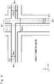
Fig. 2 is an enlarged schematic plan view of the plurality (four in the example ofFig. 2 ) ofsemiconductor chips 10 formed on the semiconductor wafer 1. As shown inFig. 2 , each of thesemiconductor chips 10 includes a circuit formation region CA1, a seal ring (first seal ring) SRI, and a seal ring (second seal ring) SR2 which have a rectangular shape. - Electronic circuit patterns and various functional blocks are arranged in the circuit formation region CA1 of each of the
semiconductor chips 10. - The seal ring SRI is formed along four outer peripheral parts of the circuit formation region CA1 so as to surround an outer periphery of the circuit formation region CA1. Hereinafter, out of the four outer peripheral parts of the circuit formation region CA1, the seal ring SRI formed along an upper side, a lower side, a right side, and a left side of the paper surface (a plus side in a y-axis direction, a minus side in a y-axis direction, a plus side in an x-axis direction, and a minus side in an x-axis direction based on the circuit formation region CA1) will be referred to as seal rings SR1_U, SR1_D, SR1_R, and SR1_L, respectively.
- An upper right corner T1_UR is formed by the respective ends of the seal rings SR1_U and SR1_R formed along the upper side and the right side of the circuit formation region CA1. An upper left corner T1_UL is formed by the respective ends of the seal rings SR1_U and SR1_L formed along the upper side and the left side of the circuit formation region CA1. A lower right corner T1_DR is formed by the respective ends of the seal rings SR1_D and SR1_R formed along the lower side and the right side of the circuit formation region CA1. A lower left corner T1_DL is formed by the respective ends of the seal rings SR1_D and SR1_L formed along the lower side and the left side of the circuit formation region CA1.
- On two sides of the four outer peripheral parts of the circuit formation region CA1, the seal ring SR2 is formed outside of the circuit formation region CA1 compared with the seal ring SRI and in parallel with the seal ring SRI. In the example of
Fig. 2 , the seal rings SR2 are formed, respectively, as seal rings SR2_U and SR2_R on two sides of the upper side and the right side of the paper surface (the plus side in the y-axis direction and the plus side in the x-axis direction based on the circuit formation region CA1) out of the four outer peripheral parts of the circuit formation region CA1. - In addition, the seal ring SR2 is formed to contact with a part of the seal ring SRI. In the example of
Fig. 2 , the seal ring SR2 is further formed from a lower right end T2_DR to the corner T1_DR of the seal ring SRI, and further formed from an upper left end T2_UL to the corner T1_UL of the seal ring SRI. Therefore, each of the corners T1_DR and T1_UL has a T-shape in a plan view. - Here, between the
semiconductor chips 10 adjacent to each other, two types of dicing lines DL1 and DL2 are defined by the seal rings SRI and SR2. Specifically, the dicing line DL1 is defined by a set of seal rings SRI facing each other between thesemiconductor chips 10 adjacent to each other. The dicing line DL2 is defined by a set of seal rings SRI and SR2 facing each other between thesemiconductor chips 10 adjacent to each other. In the example ofFig. 2 , a width of the dicing line DL1 is larger than a width of the dicing line DL2. - Thus, in the semiconductor wafer 1 in which a common circuit pattern is formed, the plurality of
semiconductor chips 10 can be cut out along any one arbitrarily selected from the two types of different dicing lines DL1 and DL2 (more specifically, center lines CL1 and CL2 of the dicing lines DL1 and DL2). - Here, since performance and design constraint of a dicer differ from depending on a user, dicing conditions of the semiconductor wafer (specifically, the widths of the dicing lines of the semiconductor wafer) vary depending on the user. In the semiconductor wafer 1 according to the present embodiment, the dicing lines used for dicing can be changed according to a request of such a user.
- For example, even when a user U1 requests a semiconductor wafer having a dicing line width wider than that of a user U2, semiconductor wafers having different dicing line widths need not to be individually prepared for the users U1 and U2, and a common semiconductor wafer 1 may be provided. In this case, the user U1 may cut out the plurality of
semiconductor chips 10 along the dicing line DL1 having a wide width from the semiconductor wafer 1. Further, the user U2 may cut out the plurality ofsemiconductor chips 10 along the dicing line DL2 having a narrow width from the semiconductor wafer 1. - As described above, in the semiconductor wafer 1 according to the present embodiment, the plurality of seal rings SRI and SR2 are formed on each of the plurality of
semiconductor chips 10 formed in a matrix. In the semiconductor wafer 1 according to the present embodiment, that is, the plurality of different dicing lines DL1 and DL2 are defined between the semiconductor chips 10 adjacent to each other. Thereby, in the semiconductor wafer 1 according to the present embodiment, the plurality ofsemiconductor chips 10 can be cut out along any one arbitrarily selected from two different types of dicing lines DL1 and DL2. In the semiconductor wafer 1 according to the present embodiment, that is, the dicing line used for dicing can be changed according to the request of the user. Even when dicing is performed along any of the dicing lines DL1 and DL2, at least the seal ring SRI remains, so that an effect of circuit deterioration prevention due to the seal ring SRI is maintained. - In the semiconductor wafer 1 according to the present embodiment, even when dicing is performed along any of the dicing lines DL1 and DL2, a size of each of the
semiconductor chip 10 does not change. For this reason, even when dicing is performed along any of the dicing lines DL1 and DL2, the number ofsemiconductor chips 10 cut out from the semiconductor wafer 1 does not change. - The case has been described in the present embodiment in which the seal ring SR2 is formed on the two sides of the upper side and the right side out of the four outer peripheral parts of the circuit formation region CA1 in each of the semiconductor chips 10, but the seal ring SR2 may be formed on any two sides without being limited thereto.
- Further, each of the width (a length in the y-axis direction) of the dicing line DL1 extending in the x-axis direction and the width (a length in the x-axis direction) of the dicing line DL1 extending in the y-axis direction can be set to any length. Similarly, each of the width (a length in the y-axis direction) of the dicing line DL2 extending in the x-axis direction and the width (a length in the x-axis direction) of the dicing line DL2 extending in the y-axis direction can be set to any length.
-
Fig. 3 is a schematic cross-sectional view of the seal ring SRI and a peripheral region thereof. A cross-sectional structure of the seal ring SR2 is the same as that of the seal ring SRI, and thus will not be described. - As shown in
Fig. 3 , the seal ring SRI is formed in a height direction (z-axis direction) by metals M1 to M5 laminated on a silicon substrate of the semiconductor wafer 1, a contact C1 for connecting between the silicon substrate and the metal M1, and vias VI to V4 for connecting between the metals M1 to M5. -
Fig. 4 is a schematic plan view of the seal rings SRI and SR2 and dummy patterns DM arranged in the vicinity of the seal rings SRI and SR2. In the example ofFig. 4 , while only a wiring layer of the metal M1 is shown, wiring layers of the metals M2 to M5 basically have the same configuration of the wiring layer of the metal M1. - Here, the contact and the vias used in each of the semiconductor chips 10 are usually determined to have a uniform minimum width and the like so as to satisfy design constraints. However, the seal rings SRI and SR2 are formed to surround the outer periphery of the circuit formation region CA1 in a plan view without being bound by such design constraints. The T-shaped corner of the seal ring SRI is also formed without being bound by the design constraints.
- In addition, as shown in
Figs. 3 and4 , the dummy patterns DM are formed in regions, in which the circuit pattern is not formed, in the peripheral regions of the seal rings SRI and SR2. The dummy patterns DM are also formed in a region surrounded by the seal rings SRI and SR2. Thereby, even when dicing is performed along any of the dicing lines DL1 and DL2, a coverage (distribution of the metals) of each of the semiconductor chips 10 can be made uniform. In reality, the dummy patterns DM are formed on the wiring layers of the metals M1 to M5, and are not formed on layers in which the contact and the vias are formed. - In addition, the center line CL1 of the dicing line DL1 may enter the region surrounded by the seal rings SRI and SR2 due to a difference in the widths of the seal rings SRI and SR2. In this case, when dicing is performed along the center line CL1 of the dicing line DL1, the inside of the region surrounded by the seal rings SRI and SR2 is cut by the dicing. However, even in such a case, since a step between the inside and the outside of the region surrounded by the seal rings SRI and SR2 is not formed by the dummy pattern DM formed in the region, the dicing can be realized with high accuracy.
- Further, a TEG (Test Element Group) and an alignment mark may be formed in the region surrounded by the seal rings SRI and SR2. Thereby, signal noise generated when light is incident on the TEG and the alignment mark can be blocked by the seal ring SRI as compared with a case where the TEG and the alignment mark are formed inside the seal ring SRI.
- Subsequently, an example will be described with reference to
Figs. 5 to 8 in which each of the semiconductor chips 10 cut out from the semiconductor wafer 1 is used for forming a liquid crystal display device. -
Fig. 5 is a schematic plan view of asemiconductor chip 10a indicating thesemiconductor chip 10 used for forming a liquid crystal display device. In addition,Fig. 6 is an enlarged plan view of a part of thesemiconductor chip 10a shown inFig. 5 . - In this example, the width of the dicing line DL1 (the dicing line DL1 extending in the x-axis direction) between the semiconductor chips 10 adjacent to each other in the y-axis direction is 200 µm, and the width of the dicing line DL1 (the dicing line DL1 extending in the y-axis direction) between the semiconductor chips 10 adjacent to each other in the x-axis direction is 400 µm. In this example, the width of the dicing line DL2 (the dicing line DL2 extending in the x-axis direction) between the semiconductor chips 10 adjacent to each other in the y-axis direction is 100 µm, and the width of the dicing line DL2 (the dicing line DL2 extending in the y-axis direction) between the semiconductor chips 10 adjacent to each other in the x-axis direction is 100 µm.
- First, a pixel area PA1 arranged with a plurality of pixels P in a matrix is provided in a central part of the circuit formation region CA1 of the
semiconductor chip 10a. - A horizontal driver HD1 for driving the horizontal direction (x-axis direction) of the plurality of pixels P is arranged in a region below the pixel area PA1 (a region on the minus side in the y-axis direction based on the pixel area PA1). On the other hand, no circuit is arranged in a region above the pixel area PA1 (a region on the plus side in the y-axis direction based on the pixel area PA1), and such a region has a sufficiently available space.
- In a region on a left side of the pixel area PA1 (a region on the minus side in the x-axis direction based on the pixel area PA1), a plurality of pads PDs are arranged along the outer peripheral part of the circuit formation region CA1, and a plurality of input/output ports IOs are arranged to face the plurality of pads PDs. In addition, vertical drivers VD1 and VD2 for driving the vertical direction (y-axis direction) of the plurality of pixels P are arranged in the region on the left side of the pixel area PA1 and a region on a right side of the pixel area PA1 (a region on the plus side in the x-axis direction based on the pixel area PA1), respectively. Here, the region on the left side of the pixel area PA1 spreads with the circuit, and has no available space, but the region on the right side of the pixel area PA1 has an available space.
- A seal area SA1 is provided in a region surrounding the pixel area PA1 in the circuit formation region CA1 (see
Fig. 7 ). Spacer balls are sprayed on the seal area SA1 together with a sealant. Then, a glass CE, which is a common electrode having light transmittance, are arranged on thesemiconductor chip 10a. Thereby, a clearance is formed between thesemiconductor chip 10 and the glass CE arranged on an upper surface of thesemiconductor chip 10. When a liquid crystal is filled and encapsulated between electrodes of the plurality of pixels P and the glass CE which are arranged on thesemiconductor chip 10, a reflective liquid crystal display device is formed. - As describe above, the seal area SA1 is provided in the region surrounding the pixel area PA1 in the circuit formation region CA1. The seal area SA1 may include the vertical drivers VD1 and VD2 and the horizontal driver HD1. In the region on the right side of the pixel area PA1, an area of the vertical driver VD2 is smaller than an area of the seal area SA1. Therefore, a gap is generated between the vertical driver VD2 and the chip end in the region on the right side of the pixel area PA1.
- A size of the seal area SA1 varies depending on the user who assembles the reflective liquid crystal display device. For example, it is assumed that the user U1 needs a dicing line having a wide width but the size of the seal area SA1 may be small. On the other hand, the user U2 needs a large-sized seal area SA1, but the width of the dicing line may be narrowed. In this case, the user U1 may cut out the plurality of
semiconductor chips 10a from the semiconductor wafer 1 along the dicing line DL1 having the wide width. On the other hand, the user U2 may cut out the plurality ofsemiconductor chips 10a from the semiconductor wafer 1 along the dicing line DL2 having the narrow width. - Patent Literature 1 does not disclose or suggest that a common semiconductor wafer is diced under different dicing conditions. For this reason, according to the related technique, if the common semiconductor wafer is subjected to dicing under different dicing conditions, there is a risk that the dicing may proceed beyond the dicing line, and in this case, the seal ring may be broken. In other words, according to the related technique, the common semiconductor wafer cannot be subjected to dicing under different dicing conditions. In the semiconductor wafer 1 according to the present embodiment, such a problem can be solved.
-
Fig. 8 is an enlarged schematic plan view of a plurality (four in an example ofFig. 8 ) of semiconductor chips 20 formed on a semiconductor wafer 2 according to a second embodiment. - In each of the semiconductor chips 10 provided on the semiconductor wafer 1 shown in
Fig. 2 , the seal ring SR2 is formed on two sides out of the four outer peripheral parts of the circuit formation region CA1. On the other hand, in each of the semiconductor chips 20 provided on the semiconductor wafer 2 shown inFig. 8 , a seal ring SR2 is formed only on one side out of four outer peripheral parts of a circuit formation region CA1. - In the example of
Fig. 8 , the seal ring SR2 is formed as a seal ring SR2_R only on one side on a right side of the paper surface (a plus side in an x-axis direction based on the circuit formation region CA1) out of the four outer peripheral parts of the circuit formation region CA1. - In addition, seal ring SR2 is formed to contact with a part of a seal ring SRI. In the example of
Fig. 8 , the seal ring SR2 is further formed from one end T2_UR of the seal ring SR2_R to a corner T1_UR of the seal ring SRI, and is further formed from the other end T2_DR of the seal ring SR2_R to a corner T1_DR of the seal ring SRI. For this reason, each of the corners T1_UR and T1_DR has a T-shape in a plan view. - Thereby, between the semiconductor chips 20 adjacent to each other, two types of dicing lines DL1 and DL2 are defined by the seal rings SRI and SR2. Specifically, the dicing line DL1 is defined by a set of seal rings SRI facing each other between the semiconductor chips 20 adjacent to each other. The dicing line DL2 is defined by a set of seal rings SRI and SR2 (alternatively, SRI and SRI) facing each other between the semiconductor chips 20 adjacent to each other. In the example of
Fig. 8 , width of the dicing lines DL1 and DL2 extending in the y-axis direction are different from each other, but widths of the dicing lines DL1 and DL2 extending in the x-axis direction are equal to each other. - Other structures of the semiconductor wafer 2 are the same as those of the semiconductor wafer 1, and thus will not be described.
- As described above, in the semiconductor wafer 2 according to the present embodiment, the plurality of seal rings SRI and SR2 are formed on each of the plurality of semiconductor chips 20 formed in a matrix. In the semiconductor wafer 2 according to the present embodiment, that is, the plurality of different dicing lines DL1 and DL2 are defined between the semiconductor chips 20 adjacent to each other. Thereby, in the semiconductor wafer 2 according to the present embodiment, the plurality of semiconductor chips 20 can be cut out along any one arbitrarily selected from two different types of dicing lines DL1 and DL2. In the semiconductor wafer 3 according to the present embodiment, that is, the dicing line used for dicing can be changed according to the request of the user. Even when dicing is performed along any of the dicing lines DL1 and DL2, at least the seal ring SRI remains, so that an effect of circuit deterioration prevention due to the seal ring SRI is maintained.
- The case has been described in the present embodiment in which the seal ring SR2 is formed on one side of the right side out of the four outer peripheral parts of the circuit formation region CA1 in each of the semiconductor chips 20, but the seal ring SR2 may be formed on any one side without being limited thereto.
- The case has been described in the present embodiment in which the seal ring SR2 is formed only on one side out of the four outer peripheral parts of the circuit formation region CA1 in each of the semiconductor chips 20, but the seal ring SR2 may be formed on two sides as in the first embodiment or may be formed on any three sides without being limited thereto.
-
Fig. 9 is an enlarged schematic plan view of a plurality (four in an example ofFig. 9 ) of semiconductor chips 30 formed on a semiconductor wafer 3 according to a third embodiment. - In each of the semiconductor chips 10 provided on the semiconductor wafer 1 shown in
Fig. 2 , the seal ring SR2 is formed on two sides out of the four outer peripheral parts of the circuit formation region CA1. On the other hand, in each of the semiconductor chips 30 provided on the semiconductor wafer 3 shown inFig. 9 , a seal ring SR2 is formed along four outer peripheral parts of a circuit formation region CA1 so as to surround an outer periphery of the circuit formation region CA1. - In addition, seal ring SR2 is formed to contact with a part of a seal ring SRI. In the example of
Fig. 9 , seal rings are further formed from four corners of the seal ring SRI to peripheral parts of four corners of the seal ring SR2. For this reason, on the peripheral parts of the corners, T-shaped or cross-shaped seal rings are formed. - Thereby, between the semiconductor chips 30 adjacent to each other, two types of dicing lines DL1 and DL2 are defined by the seal rings SRI and SR2. Specifically, the dicing line DL1 is defined by a set of seal rings SRI facing each other between the semiconductor chips 30 adjacent to each other. The dicing line DL2 is defined by a set of seal ring SR2 facing each other between the semiconductor chips 30 adjacent to each other.
- Other structures of the semiconductor wafer 3 are the same as those of the semiconductor wafer 1, and thus will not be described.
- As described above, in the semiconductor wafer 3 according to the present embodiment, the plurality of seal rings SRI and SR2 are formed on each of the plurality of semiconductor chips 30 formed in a matrix. In the semiconductor wafer 3 according to the present embodiment, that is, the plurality of different dicing lines DL1 and DL2 are defined between the semiconductor chips 30 adjacent to each other. Thereby, in the semiconductor wafer 3 according to the present embodiment, the plurality of semiconductor chips 30 can be cut out along any one arbitrarily selected from two different types of dicing lines DL1 and DL2. In the semiconductor wafer 3 according to the present embodiment, that is, the dicing line used for dicing can be changed according to the request of the user. Even when dicing is performed along any of the dicing lines DL1 and DL2, at least the seal ring SRI remains, so that an effect of circuit deterioration prevention due to the seal ring SRI is maintained.
- This application is based upon and claims the benefit of priority from
Japanese Patent Application No. 2019-112648, filed on June 18, 2019 - The present invention can be suitably applied to the manufacture of semiconductor chips used in a liquid crystal display device.
-
- 1 SEMICONDUCTOR WAFER
- 2 SEMICONDUCTOR WAFER
- 3 SEMICONDUCTOR WAFER
- 10 SEMICONDUCTOR CHIP
- 10a SEMICONDUCTOR CHIP
- 20 SEMICONDUCTOR CHIP
- 30 SEMICONDUCTOR CHIP
- CA1 CIRCUIT FORMATION REGION
- C1 CONTACT
- CE GLASS
- CL1, CL2 CENTER LINE
- DL1 DICING LINE
- DL2 DICING LINE
- DM DUMMY PATTERN
- HD1 HORIZONTAL DRIVER
- IO INPUT/OUTPUT PORT
- M1 to M5 METAL
- P PIXEL
- PA1 PIXEL AREA
- PD PAD
- SA1 SEAL AREA
- SRI SEAL RING
- SR2 SEAL RING
- SR1_U, SR1_D, SR1_R, SR1_L SEAL RING
- SR2_U, SR2_R SEAL RING
- T1_UR, T1_UL, T1_DR, T1_DL CORNER
- T2_UR, T2_UL, T2_DR END (CORNER)
- VI to V4 VIA
- VD1, VD2 VERTICAL DRIVER
Claims (5)
- A semiconductor wafer comprising:a rectangular circuit formation region provided on the semiconductor wafer;an electronic circuit formed in the circuit formation region;a first seal ring formed along each of four outer peripheral parts of the circuit formation region so as to surround an outer periphery of the circuit formation region; anda second seal ring formed, in parallel with the first seal ring, on outer peripheral parts other than at least one outer peripheral part out of the four outer peripheral parts of the circuit formation region.
- The semiconductor wafer according to Claim 1, wherein a plurality of the rectangular circuit formation regions partitioned in a matrix are provided on the semiconductor wafer.
- The semiconductor wafer according to Claim 1 or 2, wherein the second seal ring is formed to contact with a part of the first seal ring.
- The semiconductor wafer according to any one of Claims 1 to 3, wherein a dummy pattern is formed in a region surrounded by the first seal ring and the second seal ring.
- A method of manufacturing a semiconductor chip comprising:
cutting out semiconductor chips by performing dicing along any of a first dicing line defined by the first seal rings provided between the circuit formation regions adjacent to each other and a second dicing line defined using at least the second seal ring of the first seal ring and the second seal ring provided between the adjacent circuit formation regions, using a semiconductor wafer including:a plurality of rectangular circuit formation regions partitioned in a matrix on a semiconductor wafer;an electronic circuit formed in each of the circuit formation regions;a first seal ring formed along each of four outer peripheral parts of each of the circuit formation regions so as to surround an outer periphery of the circuit formation region; anda second seal ring formed, in parallel with the first seal ring, on outer peripheral parts other than at least one outer peripheral part out of the four outer peripheral parts of each of the circuit formation regions.
Applications Claiming Priority (2)
| Application Number | Priority Date | Filing Date | Title |
|---|---|---|---|
| JP2019112648A JP7218678B2 (en) | 2019-06-18 | 2019-06-18 | Method for manufacturing semiconductor wafer and semiconductor chip |
| PCT/JP2020/018506 WO2020255573A1 (en) | 2019-06-18 | 2020-05-07 | Semiconductor wafer and manufacturing method for semiconductor chip |
Publications (2)
| Publication Number | Publication Date |
|---|---|
| EP3989265A1 true EP3989265A1 (en) | 2022-04-27 |
| EP3989265A4 EP3989265A4 (en) | 2022-07-27 |
Family
ID=73838096
Family Applications (1)
| Application Number | Title | Priority Date | Filing Date |
|---|---|---|---|
| EP20825941.6A Pending EP3989265A4 (en) | 2019-06-18 | 2020-05-07 | SEMICONDUCTOR WAFER AND SEMICONDUCTOR CHIP FABRICATION METHOD |
Country Status (6)
| Country | Link |
|---|---|
| US (1) | US12243831B2 (en) |
| EP (1) | EP3989265A4 (en) |
| JP (1) | JP7218678B2 (en) |
| KR (1) | KR102728695B1 (en) |
| CN (1) | CN113950734B (en) |
| WO (1) | WO2020255573A1 (en) |
Families Citing this family (1)
| Publication number | Priority date | Publication date | Assignee | Title |
|---|---|---|---|---|
| JP2023036453A (en) * | 2021-09-02 | 2023-03-14 | キオクシア株式会社 | Semiconductor device |
Family Cites Families (26)
| Publication number | Priority date | Publication date | Assignee | Title |
|---|---|---|---|---|
| JP2000124158A (en) * | 1998-10-13 | 2000-04-28 | Mitsubishi Electric Corp | Semiconductor wafer and semiconductor device |
| JP2002134506A (en) | 2000-10-19 | 2002-05-10 | Mitsubishi Electric Corp | Semiconductor device |
| JP2002217196A (en) * | 2001-01-17 | 2002-08-02 | Mitsubishi Electric Corp | Semiconductor device and method of manufacturing the same |
| TW529097B (en) * | 2002-01-28 | 2003-04-21 | Amic Technology Taiwan Inc | Scribe lines for increasing wafer utilizable area |
| JP2004153015A (en) | 2002-10-30 | 2004-05-27 | Fujitsu Ltd | Semiconductor device and manufacturing method thereof |
| JP4502173B2 (en) * | 2003-02-03 | 2010-07-14 | ルネサスエレクトロニクス株式会社 | Semiconductor device and manufacturing method thereof |
| JP4222979B2 (en) * | 2004-07-28 | 2009-02-12 | Necエレクトロニクス株式会社 | Semiconductor device |
| KR100498708B1 (en) | 2004-11-08 | 2005-07-01 | 옵토팩 주식회사 | Electronic package for semiconductor device and packaging method thereof |
| FR2896684B1 (en) * | 2006-02-01 | 2008-09-26 | Tornier Soc Par Actions Simplifiee | TIBIAL IMPLANT WITH OFFSET SHAFT |
| JP5061520B2 (en) * | 2006-07-18 | 2012-10-31 | 富士通セミコンダクター株式会社 | Semiconductor device and semiconductor wafer |
| JP2008053559A (en) | 2006-08-25 | 2008-03-06 | Matsushita Electric Ind Co Ltd | Semiconductor device and manufacturing method thereof |
| KR100995558B1 (en) * | 2007-03-22 | 2010-11-22 | 후지쯔 세미컨덕터 가부시키가이샤 | Semiconductor device and manufacturing method of semiconductor device |
| JP5326282B2 (en) | 2008-01-10 | 2013-10-30 | 富士通セミコンダクター株式会社 | Semiconductor device, method of manufacturing the same, and exposure mask |
| US8242586B2 (en) * | 2008-09-09 | 2012-08-14 | Mediatek Inc. | Integrated circuit chip with seal ring structure |
| US7906836B2 (en) * | 2008-11-14 | 2011-03-15 | Taiwan Semiconductor Manufacturing Company, Ltd. | Heat spreader structures in scribe lines |
| CA3220110A1 (en) | 2009-12-22 | 2011-07-21 | The Chemours Company Fc, Llc | Compositions comprising 2,3,3,3-tetrafluoropropene, 1,1,2,3-tetrachloropropene, 2-chloro-3,3,3-trifluoropropene, or 2-chloro-1,1,1,2-tetrafluoropropane |
| CN102918637A (en) | 2011-01-14 | 2013-02-06 | 松下电器产业株式会社 | Semiconductor devices and flip-chip mounting parts |
| JP5837783B2 (en) * | 2011-09-08 | 2015-12-24 | ルネサスエレクトロニクス株式会社 | Semiconductor integrated circuit device |
| JP2013201293A (en) | 2012-03-26 | 2013-10-03 | Toshiba Corp | Semiconductor storage device |
| US8729664B2 (en) * | 2012-04-02 | 2014-05-20 | International Business Machines Corporation | Discontinuous guard ring |
| US8785246B2 (en) * | 2012-08-03 | 2014-07-22 | Plx Technology, Inc. | Multiple seal-ring structure for the design, fabrication, and packaging of integrated circuits |
| CN102832178A (en) | 2012-09-18 | 2012-12-19 | 上海工程技术大学 | Sealing ring structure used for integrated circuit chip |
| JP6061726B2 (en) | 2013-02-26 | 2017-01-18 | ルネサスエレクトロニクス株式会社 | Semiconductor device and semiconductor wafer |
| JP2015088576A (en) * | 2013-10-30 | 2015-05-07 | ルネサスエレクトロニクス株式会社 | Semiconductor device and method of manufacturing the same |
| JP6230676B2 (en) | 2016-10-11 | 2017-11-15 | ルネサスエレクトロニクス株式会社 | Semiconductor device |
| CN109148559A (en) * | 2017-06-28 | 2019-01-04 | 矽创电子股份有限公司 | Wafer structure |
-
2019
- 2019-06-18 JP JP2019112648A patent/JP7218678B2/en active Active
-
2020
- 2020-05-07 WO PCT/JP2020/018506 patent/WO2020255573A1/en not_active Ceased
- 2020-05-07 KR KR1020217040714A patent/KR102728695B1/en active Active
- 2020-05-07 EP EP20825941.6A patent/EP3989265A4/en active Pending
- 2020-05-07 CN CN202080043023.4A patent/CN113950734B/en active Active
-
2021
- 2021-12-16 US US17/553,690 patent/US12243831B2/en active Active
Also Published As
| Publication number | Publication date |
|---|---|
| WO2020255573A1 (en) | 2020-12-24 |
| US20220108958A1 (en) | 2022-04-07 |
| KR102728695B1 (en) | 2024-11-08 |
| KR20220007164A (en) | 2022-01-18 |
| CN113950734B (en) | 2025-04-11 |
| US12243831B2 (en) | 2025-03-04 |
| JP7218678B2 (en) | 2023-02-07 |
| JP2020205363A (en) | 2020-12-24 |
| EP3989265A4 (en) | 2022-07-27 |
| CN113950734A (en) | 2022-01-18 |
Similar Documents
| Publication | Publication Date | Title |
|---|---|---|
| US20250132299A1 (en) | Light emitting device | |
| CN100536119C (en) | Semiconductor device and method for manufacturing the same | |
| KR102714981B1 (en) | Integrated circuit chip, and integrated circuit package and display apparatus including integrated circuit chip | |
| CN100377353C (en) | semiconductor substrate | |
| CN101154661A (en) | Semiconductor device | |
| US20080083959A1 (en) | Stacked structures and methods of forming stacked structures | |
| JP2010074106A (en) | Semiconductor chip, semiconductor wafer, and method of dicing the same | |
| WO2010024015A1 (en) | Semiconductor element and display device provided with the same | |
| JP5425363B2 (en) | Semiconductor device and display device | |
| US12243831B2 (en) | Semiconductor wafer and method of manufacturing semiconductor chip | |
| KR101904730B1 (en) | Tape pakage and display apparatus having the same | |
| JP2009115940A (en) | Liquid crystal panel | |
| CN101145565A (en) | Multi-chamfer thin film transistor array substrate and liquid crystal display device | |
| JP3564971B2 (en) | Tape carrier package | |
| JP2005136329A (en) | Semiconductor device | |
| JP2002124537A (en) | Semiconductor chip bonding structure and display device having the structure | |
| US10497679B2 (en) | Wafer level package and wafer level chip size package | |
| JP2010175700A (en) | Liquid crystal display | |
| KR102403730B1 (en) | Semiconductor chip and semiconductor package including the same | |
| KR102443830B1 (en) | Method of routing electrical wiring and its structure | |
| JP2005099709A (en) | Method for manufacturing electrooptical device, method for parting a plurality of substrates, substrate for electrooptical device, and electrooptical device | |
| JP2005292505A (en) | Display panel, IC chip, and manufacturing method thereof | |
| KR100824533B1 (en) | Display driving chip | |
| KR102088920B1 (en) | Film for use in COF Package with 2-layer Pattern | |
| JP2000321589A (en) | Display panel |
Legal Events
| Date | Code | Title | Description |
|---|---|---|---|
| STAA | Information on the status of an ep patent application or granted ep patent |
Free format text: STATUS: THE INTERNATIONAL PUBLICATION HAS BEEN MADE |
|
| PUAI | Public reference made under article 153(3) epc to a published international application that has entered the european phase |
Free format text: ORIGINAL CODE: 0009012 |
|
| STAA | Information on the status of an ep patent application or granted ep patent |
Free format text: STATUS: REQUEST FOR EXAMINATION WAS MADE |
|
| 17P | Request for examination filed |
Effective date: 20220114 |
|
| AK | Designated contracting states |
Kind code of ref document: A1 Designated state(s): AL AT BE BG CH CY CZ DE DK EE ES FI FR GB GR HR HU IE IS IT LI LT LU LV MC MK MT NL NO PL PT RO RS SE SI SK SM TR |
|
| A4 | Supplementary search report drawn up and despatched |
Effective date: 20220624 |
|
| RIC1 | Information provided on ipc code assigned before grant |
Ipc: H01L 23/58 20060101ALI20220620BHEP Ipc: H01L 23/00 20060101ALI20220620BHEP Ipc: H01L 21/78 20060101AFI20220620BHEP |
|
| DAV | Request for validation of the european patent (deleted) | ||
| DAX | Request for extension of the european patent (deleted) |