EP3987418B1 - System und verfahren zur sicherung elektronischer vorrichtungen - Google Patents
System und verfahren zur sicherung elektronischer vorrichtungen Download PDFInfo
- Publication number
- EP3987418B1 EP3987418B1 EP20833038.1A EP20833038A EP3987418B1 EP 3987418 B1 EP3987418 B1 EP 3987418B1 EP 20833038 A EP20833038 A EP 20833038A EP 3987418 B1 EP3987418 B1 EP 3987418B1
- Authority
- EP
- European Patent Office
- Prior art keywords
- processing unit
- message
- hardware
- software
- logic
- Prior art date
- Legal status (The legal status is an assumption and is not a legal conclusion. Google has not performed a legal analysis and makes no representation as to the accuracy of the status listed.)
- Active
Links
Images


Classifications
-
- G—PHYSICS
- G06—COMPUTING OR CALCULATING; COUNTING
- G06F—ELECTRIC DIGITAL DATA PROCESSING
- G06F21/00—Security arrangements for protecting computers, components thereof, programs or data against unauthorised activity
- G06F21/50—Monitoring users, programs or devices to maintain the integrity of platforms, e.g. of processors, firmware or operating systems
- G06F21/52—Monitoring users, programs or devices to maintain the integrity of platforms, e.g. of processors, firmware or operating systems during program execution, e.g. stack integrity ; Preventing unwanted data erasure; Buffer overflow
- G06F21/54—Monitoring users, programs or devices to maintain the integrity of platforms, e.g. of processors, firmware or operating systems during program execution, e.g. stack integrity ; Preventing unwanted data erasure; Buffer overflow by adding security routines or objects to programs
-
- G—PHYSICS
- G06—COMPUTING OR CALCULATING; COUNTING
- G06F—ELECTRIC DIGITAL DATA PROCESSING
- G06F21/00—Security arrangements for protecting computers, components thereof, programs or data against unauthorised activity
- G06F21/50—Monitoring users, programs or devices to maintain the integrity of platforms, e.g. of processors, firmware or operating systems
- G06F21/57—Certifying or maintaining trusted computer platforms, e.g. secure boots or power-downs, version controls, system software checks, secure updates or assessing vulnerabilities
- G06F21/572—Secure firmware programming, e.g. of basic input output system [BIOS]
-
- G—PHYSICS
- G06—COMPUTING OR CALCULATING; COUNTING
- G06F—ELECTRIC DIGITAL DATA PROCESSING
- G06F21/00—Security arrangements for protecting computers, components thereof, programs or data against unauthorised activity
- G06F21/50—Monitoring users, programs or devices to maintain the integrity of platforms, e.g. of processors, firmware or operating systems
- G06F21/55—Detecting local intrusion or implementing counter-measures
- G06F21/554—Detecting local intrusion or implementing counter-measures involving event detection and direct action
-
- G—PHYSICS
- G06—COMPUTING OR CALCULATING; COUNTING
- G06F—ELECTRIC DIGITAL DATA PROCESSING
- G06F21/00—Security arrangements for protecting computers, components thereof, programs or data against unauthorised activity
- G06F21/70—Protecting specific internal or peripheral components, in which the protection of a component leads to protection of the entire computer
- G06F21/71—Protecting specific internal or peripheral components, in which the protection of a component leads to protection of the entire computer to assure secure computing or processing of information
- G06F21/76—Protecting specific internal or peripheral components, in which the protection of a component leads to protection of the entire computer to assure secure computing or processing of information in application-specific integrated circuits [ASIC] or field-programmable devices, e.g. field-programmable gate arrays [FPGA] or programmable logic devices [PLD]
-
- G—PHYSICS
- G06—COMPUTING OR CALCULATING; COUNTING
- G06F—ELECTRIC DIGITAL DATA PROCESSING
- G06F2221/00—Indexing scheme relating to security arrangements for protecting computers, components thereof, programs or data against unauthorised activity
- G06F2221/03—Indexing scheme relating to G06F21/50, monitoring users, programs or devices to maintain the integrity of platforms
- G06F2221/034—Test or assess a computer or a system
Definitions
- the present invention generally relates to the field of data security in embedded computing systems, and more specifically to the architecture of hardware-based security solutions for embedded systems.
- the communication protocol also plays an important role in security schemes. It makes no sense to build a strong security mechanism on the end-nodes of the network or on the server where the information is sent in an open manner or using a weak protocol.
- Document US2019/049912 A1 discloses an apparatus to implement functional safety control logic (FSCL) in an autonomous driving system.
- Document US2013/346814 A1 relates to systems and methods for testing communications networks, services, and devices, e.g., testing the traffic-handling performance and/or security of the network, network accessible devices, cloud services, and data center services.
- the present invention provides a system for authenticating securing message/instruction transmission according to an authorization level, the system comprising:
- said logic comparison hardware module is comprised of an array of at least one logic gate.
- said logic comparison hardware module is implemented as a processing unit.
- the hardware processing unit includes a firmware and a memory, wherein the hardware processing is executed based on instruction in the firmware and memory modules.
- the original message is split into two messages, wherein a first message is directed to the software processing unit and a second message is directed to the hardware processing unit.
- the hardware processing unit is implemented as an Application-Specific hardware as at least one of: FPGA, ASIC.
- the system further comprises a second logic gate component configured to receive the outcome of the first logic hardware component and sending feed back to the software processing unit, wherein the feedback enables resetting operation on the software processing unit.
- the system further comprises a second logic gate component configured to Identify a malfunction if the results from the software processing unit is not compliant with hardware processing unit.
- the message directed to the software processing unit includes an encrypted message B and an encrypted CRC or HASH C of plain original message and the Software Processing Unit is configured to send the encrypted message B to the Hardware Processing Unit where the Processing Unit sends also encrypted CRC (or HASH) to the logic comparison module,
- the Hardware Processing unit calculates an encrypted CRC or HASH X by the encrypted message B and by applying a set of instructions and sends the result value X to the logic comparison module.
- security elements are initialized and activated at different stages of design, manufacture and execution, wherein non-configurable hardware element remains unchanged throughout the life circle after design and manufacture and Software, also, can be initialized on different operation stages.
- the ASIC initialization is performed only on manufacturing stage.
- the microprocessor initialization is performed in operational (exploitation) stage.
- the present invention discloses a system for authenticating and securing message/instruction transmission, wherein the system comprises:
- the testing is performed simultaneously at the hardware processing unit and the software processing unit.
- said logic comparison module is implemented as a hardware module comprising a gates array including at least one logic gate.
- said logic comparison module is implemented as a processing unit.
- the hardware processing unit includes a firmware and a memory, wherein the hardware processing is executed based on instructions in the firmware and memory modules.
- the original message is split into two messages, wherein a first message is directed to the software processing unit and a second message is directed to the hardware processing unit.
- the hardware processing unit is implemented as an Application-Specific hardware.
- the system further comprises a second logic comparison hardware module for receiving the outcome of the first logic comparison module and sending feedback to the software processing unit, wherein the feedback enables resetting operation on the software processing unit.
- the message directed to the software processing unit includes an encrypted message B and an encrypted CRC or HASH C of a plain original message and the Software Processing Unit sends the encrypted message B to the Hardware Processing Unit where the Software Processing Unit sends also encrypted CRC or HASH to the logic comparison module.
- the Hardware Processing unit calculates an encrypted CRC or HASH X by the encrypted message B and by applying a set of instructions and sends the result value X to the logic comparison module.
- the security elements are initialized and activated at different stages of design, manufacture and execution, wherein non-configurable hardware element remains unchanged throughout the life circle after design and manufacture and software element, also, can be initialized on different operation stages.
- the initialization of the hardware processing unit is performed only on manufacturing stage.
- the initialization of the hardware processing unit is performed only in operational (exploitation) stage.
- the testing at the hardware processing unit and at the software processing unit are performed in real-time.
- the present invention provides a security of embedded system composed of several components, such as separated execution environment, crypto-processor, security memory and communication protocol. Each of these components solves certain weakness, their combination creates reliable security system .
- One of the security design principles is the need to design as security system in which the different security elements are initialized and activated at different stages of design, manufacture and execution.
- non-configurable hardware element remains unchanged throughout the life circle after design and manufacture.
- End-user can't change such type of element, or part of it.
- Software allows to use configurable hardware elements. Such elements can be configured by end-user, and they are unique for each user or group of users.
- Software solutions are very flexible, as they allow to change not only configuration parameters, but also algorithms executable instructions.
- Software also, can be initialized on different operation stages. For example, crypto-algorithms can be implemented on FPGA or ASIC or on any other Application-Specific Hardware at manufacture stage.
- Secret keys can be stored in the protected memory by end-user.
- the present invention discloses a system, which is configured to implement "security as an embedded service”; a term that is utilized to describe a Software Execution Environment (SEE) that is embedded in hardware architecture, and provides built-in, multiple levels of data protection and security controls.
- SEE Software Execution Environment
- the present invention addresses the security needs of a wide range of devices, intended for deployment by various types of consumers, including for example devices employed for industrial, military or medical applications.
- the system is comprised of separate hardware modules
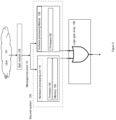
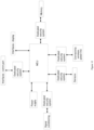
- Figure 1 presents a schematic block diagram and flow of the secured system according to one embodiment of the present invention.
- the secured system 100 is comprised of Hardware processing unit 110 and Software processing Module 120, which receive the same user nonrandom message /instruction 10 to be validated.
- the Hardware processing unit 110 which can be implemented as ASIC or FPGA process the received message or instruction and results outcome X, at the same time the software processing unit 120 process the same message instruction by firmware 130 and results outcome Y.
- the two outcomes are compared by hardware logic array 180 which comprised of at least one hardware logic gate, the comparison result R, provide indication of the message/instruction validation, for example true/false parameter (1/0).
- the comparison may be a simple AND gate which identifies if the results are identical, or any array of logic gates which identifies logic relation between the results.
- Hardware processing unit 110 and Software processing Module 120 may be untrusted modules.
- the logic gates be implemented as integrated circuit.
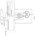
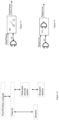
- Figure 2 presents a schematic block diagram and flow of the secured system according to one embodiment of the present invention.
- the hardware processing unit include a firmware 140 and a memory 150.
- the hardware processing is executed based on instruction in the firmware and memory module. The access to these modules is protected.
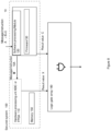
- Figure 3 presents a schematic block diagram and flow, including splitting algorithm, according to some embodiments of the present invention.
- the security system further includes a splitting module 120, which split the original user message into two different messages, one conveyed to the software processing unit and another conveyed to the hardware processing unit.
- Figure 4 presents a flow diagram, of the security process of, according to one embodiment of the present invention.
- the flow of the security process includes the following steps: User 101 sends non random message/instruction 10 transmitted to software processing module and hardware processing unit via any type of media or communication split module 125 (1005).
- the message/instruction is split, transmitting different messages to the software processing module and hardware processing unit via any type of media or communication module splitting 125.
- the system simultaneously in real time processes the message/instruction by applying set of instructions at the at software processing module by the firmware (1010) and processing the message/instruction by activating the logic gates of the hardware processing unit (1015).
- results are logically compared, the comparison, resulting logic outcome e.g. 1/0.
- outcome is calculating Resultant. (1025)
- Figure 5 presents a schematic block of the hardware implementation, of the hardware unit according to some embodiments of the present invention.
- One implementation of the hardware processing unit is of FPGA designed programmed based on predefined security algorithm to return value X based on input A.
- a second implementation of the hardware processing unit is of an ASIC unit design programmed based on predefined security algorithm to return value X based on input A
- Figure 6 presents a schematic block diagram and flow of the secured system in including resetting option according to one embodiment of the present invention.
- the system further comprises two logic gates components, where the second logic gate component is designed to provide feedback to the software processing unit, enabling reset options.
- Figure 7 presents a flow diagram, of the resetting process of, according to one embodiment of the present invention.
- the resetting process describes a mechanism in a closed loop scheme. according the following steps:
- Reset of a microcontroller does not change the state of internal memory, while in Reset state the unit is in minimum power consumption and reset to initial state.
- Sleep Line Stopes/pause the process, and continue at any time from the stopping point (breakpoint) . ( I think this item can be deleted)
- Figure 8 presents a schematic block diagram and flow of the secured system including additional message part according to one embodiment of the present invention.
- an input message may include encrypted message and encrypted CRC (or HASH) of a plain message.
- Software Processing Unit sends encrypted message to Hardware Processing Unit.
- Processing Unit sends also encrypted CRC (or HASH) to Compare Logic Unit.
- Hardware Processing Unit decrypts encrypted message, calculates CRC (or HASH), encrypts it and sends encrypted CRC (or HASH) to Compare Logic Unit.
- FIG. 9 presents a flow diagram, of the real time security process of security systems of Fig. 8 , according to one embodiment of the present invention.
- the security process according to this embodiment includes the following steps:
- the User 101 sends plain nonrandom message/instruction to software processing module including encrypted message B and encrypted CRC (or HASH) C of plain message. (3010).
- the Software Processing Unit 120 sends encrypted message B to Hardware Processing Unit 110 (3020).
- Real time Processing decrypts encrypted message B, calculates CRC (or HASH), encrypts it and sends encrypted CRC or HASH by activating logic gates of hardware module. (3030).
- Figure 10 presents a schematic block diagram and flow of the secured system including message splitting according to one embodiment of the present invention.
- Hardware Processing Unit 110 can include Table of user's shared secrets in the security memory 150.
- message 401 can include encrypted message 402, user's ID 405 and encrypted CRC (or HASH) 403 of plain message.
- Software Processing Unit 120 will send encrypted message 402 and user's ID 405 to Hardware Processing Unit 110.
- Hardware Processing Unit 110 will decrypt message 402 with corresponding user key and sends encrypted CRC (or HASH) 404 to Compare Logic Unit 108 .
- ASIC initialization on manufacturing stage
- microprocessor initialization in operational stage
- the first microprocessor with available remote update and the second microprocessor, only with local update.
- Data processing in software for example, microprocessor
- data processing in deterministic hardware components for example, logic gate.
- Deterministic hardware component is same to application-specific hardware
- the protocol defines program code of software unit, structure of hardware unit and structure of comparison unit.
- Figure 11 presents a flow diagram, of the security process of security systems of Fig. 10 , according to one embodiment of the present invention.
- Figure 1 2 presents a schematic block diagram illustrating an example of integrating the secured system within factory infrastructure according to one embodiment of the present invention.
- the security systems as described in various embodiments above can be integrated in communication line of factory infrastructures between, the media control unit (MCU) and the actuator, such as valve or pump., or between the MCU and memory unit. or MCU and signaling condition units.
- MCU media control unit
- the actuator such as valve or pump.
- Figure 1 3 presents a schematic block diagram illustrating an example of integrating the secured system within factory infrastructure according to one embodiment of the present invention
- Figure 14 presents a schematic block diagram illustrating an example of integrating the secured system within processing unit according to one embodiment of the present invention
- the output signal can be used as input signal in a switch, which control Data Line of processing unit.
- the system can be used for clipping unauthorized messages. We can change Data Line to Power Line.
- the system can completely shut off all resources, includes processor and memory.
- Figure 15 presents a schematic block diagram illustrating an example of integrating the secured system within processing unit as reset line, according to one embodiment of the present invention
- the output signal can be used as the input signal into Compare Logic unit which is located, for example, on the Reset Line.
- the system of the present invention may include, according to certain embodiments of the invention, machine readable memory containing or otherwise storing a program of instructions which, when executed by the machine, implements some or all of the apparatus, methods, features and functionalities of the invention shown and described herein.
- the apparatus of the present invention may include, according to certain embodiments of the invention, a program as above which may be written in any conventional programming language, and optionally a machine for executing the program such as but not limited to a general purpose computer which may optionally be configured or activated in accordance with the teachings of the present invention. Any of the teachings incorporated herein may wherever suitable operate on signals representative of physical objects or substances.
- Figs 15 , 16 and 17 disclose use case example - A system 300 comprising an ECU 350 and an administration control unit (Admin unit) 340, protected by the secured system 301 described in the invention.
- Administration control unit e.g., Admin unit
- Figs 15 , 16 and 17 disclose use case example - A system 300 comprising an ECU 350 and an administration control unit (Admin unit) 340, protected by the secured system 301 described in the invention.
- Admin unit administration control unit
- operational data will reach the system from authorized users with known ID and administrative data from authorized administrators with known ID.
- the function of the protection switch is to verify that authorized messages reach their corresponding addressee within the protected unit and that unauthorized messages will be blocked.
- HW unit Fig. 15
- SW unit the SW unit as well
- the encrypted message 12 can be send directly from input A 10 to the switch 330 ( Fig. 17 ).
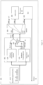
- FIG. 15 User sends message to ECU.
- Message comprises user ID, encrypted message, encrypted CRC.
- the message reaches the protection switch described in the invention
- User (101) sends message/instruction (A10) comprising (11)(12)(13) to SW processing module (120) and HW processing unit (110) simultaneously SW unit within the Switch sends the encrypted CRC to the logic gate SW processing module (120) sends E(CRC)(13) and ID(11) as Res1(Y30) to logic gate array (180)
- HW unit decrypts the message using a decryption key corresponding to sender ID and calculates a CRC for the decrypted message
- HW processing unit (110) decrypts E(M)(12) using decryption key(321) corresponding to ID(11), calculates CRC to decrypted message and encrypts said CRC using same key(321).
- WH unit sends a combination of the processing result and the sender ID to the logic gate for comparison
- HW processing unit(110) sends said encrypted CRC and ID(11) as Res2(X20) to logic gate array (180)
- the product of the HW unit is compared with the encrypted CRC sent by the SW unit in the logic gate
- Logic gate array (180) compares Res1(Y30) and Res2(X20) the logic gate sends the result of the comparison forward to the switch in a message which represents one of two possible cases: Match or Mismatch.
- the switch has two inputs: Switch(330) has control input(331) and data input(332) Control line - from logic gate Data line - from HW unit The switch has 3 connectors at its output, out of which only one can be connected at any given time. The connectors are: Switch(330) has 3 possible switching positions - (333) for error, (334) for ADMIN ID and (335) for User ID 1. Admin 2. User / ECU 3.
- the HW unit sends the message forward through the switch. Switch (330) locked in one of (333), (334) or (335) positions.
- HW processing unit (110) sends message (50) to Switch (330). Message (50) reaches either Admin unit (340) or ECU (350) if switch position is (334) or (335) respectively.
- administrative data such as FW update
- Admin Unit will perform FW update in ECU Admin Unit(340) run firmware update(60) in ECU(350)
- firmware update 60
- the ECU will perform an action and send output ECU(350) perform action and sends output()
- the term "computer” should be broadly construed to cover any kind of electronic device with data processing capabilities, including, by way of non-limiting example, personal computers, servers, computing system, communication devices, processors (e.g. Digital Signal Processor (DSP), Microcontrollers, Field Programmable Gate Array (FPGA), Application Specific Integrated Circuit (ASIC), etc.) and other electronic computing devices.
- processors e.g. Digital Signal Processor (DSP), Microcontrollers, Field Programmable Gate Array (FPGA), Application Specific Integrated Circuit (ASIC), etc.
- DSP Digital Signal Processor
- FPGA Field Programmable Gate Array
- ASIC Application Specific Integrated Circuit
- software components of the present invention including programs and data may, if desired, be implemented in ROM (Read Only Memory) form including CD-ROMs, EPROMs and EEPROMs, or may be stored in any other suitable typically non-transitory computer-readable medium such as but not limited to disks of various kinds, cards of various kinds and RAMs.
- ROM Read Only Memory
- Components described herein as software may, alternatively, be implemented wholly or partly in hardware, if desired, using conventional techniques.
- components described herein as hardware may, alternatively, be implemented wholly or partly in software, if desired, using conventional techniques.
- Any computer-readable or machine-readable media described herein is intended to include non-transitory computer- or machine-readable media.
- Any computations or other forms of analysis described herein may be performed by a suitable computerized method. Any step described herein may be computer-implemented.
- the invention shown and described herein may include (a) using a computerized method to identify a solution to any of the problems or for any of the objectives described herein, the solution optionally include at least one of a decision, an action, a product, a service or any other information described herein that impacts, in a positive manner, a problem or objectives described herein; and (b) outputting the solution.
- the scope of the present invention is not limited to structures and functions specifically described herein and is also intended to include devices which have the capacity to yield a structure, or perform a function, described herein, such that even though users of the device may not use the capacity, they are, if they so desire, able to modify the device to obtain the structure or function.
- a system embodiment is intended to include a corresponding process embodiment.
- each system embodiment is intended to include a server-centered "view” or client centered “view”, or “view” from any other node of the system, of the entire functionality of the system, computer-readable medium, apparatus, including only those functionalities performed at that server or client or node.
Landscapes
- Engineering & Computer Science (AREA)
- Computer Security & Cryptography (AREA)
- Software Systems (AREA)
- Theoretical Computer Science (AREA)
- Computer Hardware Design (AREA)
- General Engineering & Computer Science (AREA)
- Physics & Mathematics (AREA)
- General Physics & Mathematics (AREA)
- Microelectronics & Electronic Packaging (AREA)
- Mathematical Physics (AREA)
- Storage Device Security (AREA)
Claims (9)
- System zur Authentifizierung und Sicherung der Übertragung von Nachrichten/Befehlen, das System umfassendeine nichtkonfigurierbare Hardware-Verarbeitungseinheit (110), die dazu ausgelegt ist, die Gültigkeit einer Originalnachricht oder eines Derivats der Originalnachricht durch Ausführen eines spezifischen Firmware-Codes derart zu testen, dass erste Testergebnisse gewonnen werden;wobei die Hardware-Verarbeitungseinheit (110) ferner dazu ausgelegt ist, während des gesamten Lebenszyklus nach Entwurf und Herstellung unverändert zu bleiben, undwobei die Initialisierung der Hardware-Verarbeitungseinheit nur in der Herstellungsphase durchgeführt wird;eine konfigurierbare Software-Verarbeitungseinheit (120), die dazu ausgelegt ist, die Gültigkeit der Originalnachricht oder eines Derivats der Originalnachricht durch Ausführen eines spezifischen Software-Codes derart zu testen, dass zweite Testergebnisse gewonnen werden;ein Aufteilungsmodul (125), das dazu ausgestaltet ist, die Originalnachricht in zwei verschiedene Nachrichten aufzuteilen, wobei eine erste Nachricht an die Software-Verarbeitungseinheit und eine zweite Nachricht an die Hardware-Verarbeitungseinheit gerichtet ist;ein erstes Logikvergleichsmodul (180), das dazu ausgestaltet ist, die ersten und der zweiten Testergebnisse logisch zu vergleichen und eine logische Beziehung zwischen den Ergebnissen zu identifizieren,wobei der Logikvergleich die Nachricht authentifiziert; undwobei das Testen gleichzeitig in der Hardware-Verarbeitungseinheit und in der Software-Verarbeitungseinheit durchgeführt wird.
- System nach Anspruch 1, wobei das Logikvergleichsmodul als ein Hardwaremodul implementiert ist, das ein Gatterfeld mit mindestens einem Logikgatter umfasst.
- System nach Anspruch 1, wobei das Logikvergleichsmodul als eine Verarbeitungseinheit implementiert ist.
- System nach Anspruch 1, wobei die Hardware-Verarbeitungseinheit eine Firmware und einen Speicher umfasst, wobei die Hardware-Verarbeitung auf der Grundlage von Befehlen in der Firmware und Speichermodulen ausgeführt wird.
- System nach Anspruch 1, wobei die Hardware-Verarbeitungseinheit als anwendungsspezifische Hardware implementiert ist.
- System nach Anspruch 1, ferner umfassend ein zweites Logikvergleichs-Hardwaremodul, das dazu ausgestaltet ist, ein Ergebnis des ersten Logikvergleichsmoduls zu empfangen, und zum Senden einer Rückmeldung an die Software-Verarbeitungseinheit, wobei die Rückmeldung einen Rücksetzvorgang auf der Software-Verarbeitungseinheit ermöglicht.
- System nach Anspruch 1, wobei die an das Software-Verarbeitungsmodul gerichtete Nachricht eine verschlüsselte Nachricht B und einen verschlüsselten CRC oder HASH C einer einfachen Originalnachricht umfasst und die Software-Verarbeitungseinheit dazu ausgestaltet ist, die verschlüsselte Nachricht B an die Hardware-Verarbeitungseinheit zu senden und zudem den verschlüsselten CRC oder HASH an das Logikvergleichsmodul zu senden, und wobei die Hardware-Verarbeitungseinheit dazu ausgestaltet ist, einen verschlüsselten CRC oder HASH X aus der verschlüsselten Nachricht B zu berechnen und durch Anwenden eines Satzes von Befehlen und ein Ergebniswert X an das Logikvergleichsmodul zu senden.
- System nach Anspruch 1, wobei Sicherheitselemente dazu ausgestaltet sind, in verschiedenen Phasen von Entwurf, Herstellung und Ausführung initialisiert und aktiviert zu werden, wobei ein nichtkonfigurierbares Hardwareelement während des gesamten Lebenszyklus nach Entwurf und Herstellung unverändert bleibt und ein Softwareelement ebenfalls in verschiedenen Betriebsstadien initialisiert werden kann.
- System nach Anspruch 1, wobei das Testen in der Hardware-Verarbeitungseinheit und in der Software-Verarbeitungseinheit in Echtzeit durchgeführt wird.
Applications Claiming Priority (2)
| Application Number | Priority Date | Filing Date | Title |
|---|---|---|---|
| IL267619A IL267619A (en) | 2019-06-24 | 2019-06-24 | Method and system for securing electronic devices |
| PCT/IL2020/050706 WO2020261271A1 (en) | 2019-06-24 | 2020-06-24 | A system and method for securing electronic devices |
Publications (4)
| Publication Number | Publication Date |
|---|---|
| EP3987418A1 EP3987418A1 (de) | 2022-04-27 |
| EP3987418A4 EP3987418A4 (de) | 2022-08-24 |
| EP3987418B1 true EP3987418B1 (de) | 2024-10-16 |
| EP3987418C0 EP3987418C0 (de) | 2024-10-16 |
Family
ID=67874142
Family Applications (1)
| Application Number | Title | Priority Date | Filing Date |
|---|---|---|---|
| EP20833038.1A Active EP3987418B1 (de) | 2019-06-24 | 2020-06-24 | System und verfahren zur sicherung elektronischer vorrichtungen |
Country Status (4)
| Country | Link |
|---|---|
| US (1) | US12099611B2 (de) |
| EP (1) | EP3987418B1 (de) |
| IL (1) | IL267619A (de) |
| WO (1) | WO2020261271A1 (de) |
Families Citing this family (1)
| Publication number | Priority date | Publication date | Assignee | Title |
|---|---|---|---|---|
| US20250224789A1 (en) * | 2024-01-04 | 2025-07-10 | Qualcomm Incorporated | Safe designation for soc safe power management |
Family Cites Families (23)
| Publication number | Priority date | Publication date | Assignee | Title |
|---|---|---|---|---|
| GB0116568D0 (en) * | 2001-07-06 | 2001-08-29 | Ncipher Corp Ltd | Firmware validation |
| US9555322B2 (en) * | 2001-08-20 | 2017-01-31 | Bally Gaming, Inc. | Local game-area network method |
| US7907531B2 (en) * | 2005-06-13 | 2011-03-15 | Qualcomm Incorporated | Apparatus and methods for managing firmware verification on a wireless device |
| US7986786B2 (en) * | 2006-11-30 | 2011-07-26 | Hewlett-Packard Development Company, L.P. | Methods and systems for utilizing cryptographic functions of a cryptographic co-processor |
| KR101017015B1 (ko) | 2008-11-17 | 2011-02-23 | (주)소만사 | 네트워크 기반 고성능 콘텐츠 보안 시스템 및 방법 |
| WO2011119985A2 (en) * | 2010-03-26 | 2011-09-29 | Maxlinear, Inc. | Firmware authentication and deciphering for secure tv receiver |
| US8819443B2 (en) * | 2012-02-14 | 2014-08-26 | Western Digital Technologies, Inc. | Methods and devices for authentication and data encryption |
| US8856600B2 (en) | 2012-06-21 | 2014-10-07 | Breakingpoint Systems, Inc. | JTAG-based programming and debug |
| US20170364911A1 (en) * | 2014-12-12 | 2017-12-21 | Cryptomathic Ltd | Systems and method for enabling secure transaction |
| CN104486169B (zh) | 2015-01-07 | 2018-07-20 | 北京华力创通科技股份有限公司 | 可重用自动检测及随机验证系统和方法 |
| GB2536209A (en) | 2015-03-03 | 2016-09-14 | Cryptomathic Ltd | Method and system for encryption |
| DE102016206630A1 (de) * | 2016-04-20 | 2017-11-09 | Robert Bosch Gmbh | Verfahren und Vorrichtung zur Vermeidung von Manipulation einer Datenübertragung |
| US10366378B1 (en) * | 2016-06-30 | 2019-07-30 | Square, Inc. | Processing transactions in offline mode |
| KR101795695B1 (ko) * | 2016-07-14 | 2017-12-01 | 주식회사 코인플러그 | 메신저 서비스를 통하여 송수신하는 데이터에 대한 기록 서비스 및 검증 서비스를 제공하는 방법, 및 이를 이용한 서버 |
| US10761951B2 (en) | 2017-12-28 | 2020-09-01 | Intel Corporation | FPGA based functional safety control logic (FFSCL) |
| US10748433B2 (en) * | 2018-01-05 | 2020-08-18 | Ge Aviation Systems Llc | Systems and methods for autonomous distress tracking in aerial vehicles |
| US10848474B2 (en) * | 2018-02-26 | 2020-11-24 | Red Hat, Inc. | Firmware validation for encrypted virtual machines |
| US11169934B2 (en) * | 2018-06-28 | 2021-11-09 | Intel Corporation | Systems, methods and apparatus for low latency memory integrity mac for trust domain extensions |
| US10824501B2 (en) * | 2019-01-07 | 2020-11-03 | Mellanox Technologies, Ltd. | Computer code integrity checking |
| CN110001553B (zh) * | 2019-02-25 | 2021-07-09 | 南京航空航天大学 | 一种汽车四向可调转向操纵装置、控制器下载方法 |
| US11018694B2 (en) * | 2019-06-10 | 2021-05-25 | Hewlett Packard Enterprise Development Lp | Fast cyclic redundancy check code generation |
| CN111625295A (zh) * | 2020-05-22 | 2020-09-04 | 苏州浪潮智能科技有限公司 | 一种嵌入式系统启动方法、装置、设备及存储介质 |
| US11968302B1 (en) * | 2023-03-24 | 2024-04-23 | Srinivas Kumar | Method and system for pre-shared key (PSK) based secure communications with domain name system (DNS) authenticator |
-
2019
- 2019-06-24 IL IL267619A patent/IL267619A/en unknown
-
2020
- 2020-06-24 EP EP20833038.1A patent/EP3987418B1/de active Active
- 2020-06-24 WO PCT/IL2020/050706 patent/WO2020261271A1/en not_active Ceased
- 2020-06-24 US US17/623,025 patent/US12099611B2/en active Active
Also Published As
| Publication number | Publication date |
|---|---|
| WO2020261271A1 (en) | 2020-12-30 |
| US20220269787A1 (en) | 2022-08-25 |
| IL267619A (en) | 2019-08-29 |
| EP3987418A4 (de) | 2022-08-24 |
| US12099611B2 (en) | 2024-09-24 |
| EP3987418A1 (de) | 2022-04-27 |
| EP3987418C0 (de) | 2024-10-16 |
Similar Documents
| Publication | Publication Date | Title |
|---|---|---|
| US20230208824A1 (en) | Device programming with system generation | |
| US8752165B2 (en) | Provisioning secrets in an unsecured environment | |
| JP6788752B2 (ja) | 機器の安全なプロビジョニングと管理 | |
| US9111098B2 (en) | System and method for managing electronic assets | |
| US7987356B2 (en) | Programmable security platform | |
| US8839004B1 (en) | Secure cloud computing infrastructure | |
| US20150188707A1 (en) | Method for safeguarding a system-on-a-chip | |
| US10621055B2 (en) | Adaptive data recovery for clustered data devices | |
| US20070074046A1 (en) | Secure microprocessor and method | |
| Sarjan et al. | Cyber-security of industrial internet of things in electric power systems | |
| US20180287801A1 (en) | Efficient device provision | |
| US11356445B2 (en) | Data access interface for clustered devices | |
| US11889002B2 (en) | Use of physical unclonable functions to prevent counterfeiting of industrial control products | |
| CN103748828A (zh) | 用于安全传输数据的系统与方法 | |
| US9003197B2 (en) | Methods, apparatus and system for authenticating a programmable hardware device and for authenticating commands received in the programmable hardware device from a secure processor | |
| EP3987418B1 (de) | System und verfahren zur sicherung elektronischer vorrichtungen | |
| Latif et al. | Hardware security modules for secure communications in the Industrial Internet of Things | |
| WO2013147732A1 (en) | Programmable logic controller having embedded dynamic generation of encryption keys | |
| CN112887261B (zh) | 通信设备与远程终端之间的数据流的防护方法、实施该方法的设备 | |
| WO2024213475A1 (en) | Method and system for controlling interconnected devices operating in an untrusted environment | |
| Gogniat et al. | Reconfigurable security support for embedded systems | |
| US20230146633A1 (en) | Systems and methods for secure communication between computing devices over an unsecured network | |
| JP7701967B2 (ja) | プログラマブルデバイスを遠隔でプログラミングするための方法 | |
| Biham et al. | K7: A Protected Protocol for Industrial Control Systems that Fits Large Organizations | |
| US20260087158A1 (en) | Device Trust System for Managing a Large Number of IoT Devices in a Distributed Environment |
Legal Events
| Date | Code | Title | Description |
|---|---|---|---|
| STAA | Information on the status of an ep patent application or granted ep patent |
Free format text: STATUS: THE INTERNATIONAL PUBLICATION HAS BEEN MADE |
|
| PUAI | Public reference made under article 153(3) epc to a published international application that has entered the european phase |
Free format text: ORIGINAL CODE: 0009012 |
|
| STAA | Information on the status of an ep patent application or granted ep patent |
Free format text: STATUS: REQUEST FOR EXAMINATION WAS MADE |
|
| 17P | Request for examination filed |
Effective date: 20220124 |
|
| AK | Designated contracting states |
Kind code of ref document: A1 Designated state(s): AL AT BE BG CH CY CZ DE DK EE ES FI FR GB GR HR HU IE IS IT LI LT LU LV MC MK MT NL NO PL PT RO RS SE SI SK SM TR |
|
| REG | Reference to a national code |
Ref legal event code: R079 Free format text: PREVIOUS MAIN CLASS: G06F0021400000 Ipc: G06F0021760000 Ref country code: DE Ref legal event code: R079 Ref document number: 602020039665 Country of ref document: DE Free format text: PREVIOUS MAIN CLASS: G06F0021400000 Ipc: G06F0021760000 |
|
| A4 | Supplementary search report drawn up and despatched |
Effective date: 20220721 |
|
| RIC1 | Information provided on ipc code assigned before grant |
Ipc: G06F 21/55 20130101ALI20220715BHEP Ipc: G06F 21/54 20130101ALI20220715BHEP Ipc: G06F 21/76 20130101AFI20220715BHEP |
|
| DAV | Request for validation of the european patent (deleted) | ||
| DAX | Request for extension of the european patent (deleted) | ||
| GRAP | Despatch of communication of intention to grant a patent |
Free format text: ORIGINAL CODE: EPIDOSNIGR1 |
|
| STAA | Information on the status of an ep patent application or granted ep patent |
Free format text: STATUS: GRANT OF PATENT IS INTENDED |
|
| INTG | Intention to grant announced |
Effective date: 20240603 |
|
| GRAS | Grant fee paid |
Free format text: ORIGINAL CODE: EPIDOSNIGR3 |
|
| GRAA | (expected) grant |
Free format text: ORIGINAL CODE: 0009210 |
|
| STAA | Information on the status of an ep patent application or granted ep patent |
Free format text: STATUS: THE PATENT HAS BEEN GRANTED |
|
| AK | Designated contracting states |
Kind code of ref document: B1 Designated state(s): AL AT BE BG CH CY CZ DE DK EE ES FI FR GB GR HR HU IE IS IT LI LT LU LV MC MK MT NL NO PL PT RO RS SE SI SK SM TR |
|
| REG | Reference to a national code |
Ref country code: GB Ref legal event code: FG4D |
|
| REG | Reference to a national code |
Ref country code: DE Ref legal event code: R096 Ref document number: 602020039665 Country of ref document: DE Ref country code: CH Ref legal event code: EP |
|
| REG | Reference to a national code |
Ref country code: IE Ref legal event code: FG4D |
|
| U01 | Request for unitary effect filed |
Effective date: 20241113 |
|
| U07 | Unitary effect registered |
Designated state(s): AT BE BG DE DK EE FI FR IT LT LU LV MT NL PT RO SE SI Effective date: 20241120 |
|
| PG25 | Lapsed in a contracting state [announced via postgrant information from national office to epo] |
Ref country code: IS Free format text: LAPSE BECAUSE OF FAILURE TO SUBMIT A TRANSLATION OF THE DESCRIPTION OR TO PAY THE FEE WITHIN THE PRESCRIBED TIME-LIMIT Effective date: 20250216 Ref country code: HR Free format text: LAPSE BECAUSE OF FAILURE TO SUBMIT A TRANSLATION OF THE DESCRIPTION OR TO PAY THE FEE WITHIN THE PRESCRIBED TIME-LIMIT Effective date: 20241016 |
|
| PG25 | Lapsed in a contracting state [announced via postgrant information from national office to epo] |
Ref country code: ES Free format text: LAPSE BECAUSE OF FAILURE TO SUBMIT A TRANSLATION OF THE DESCRIPTION OR TO PAY THE FEE WITHIN THE PRESCRIBED TIME-LIMIT Effective date: 20241016 |
|
| PG25 | Lapsed in a contracting state [announced via postgrant information from national office to epo] |
Ref country code: NO Free format text: LAPSE BECAUSE OF FAILURE TO SUBMIT A TRANSLATION OF THE DESCRIPTION OR TO PAY THE FEE WITHIN THE PRESCRIBED TIME-LIMIT Effective date: 20250116 |
|
| PG25 | Lapsed in a contracting state [announced via postgrant information from national office to epo] |
Ref country code: GR Free format text: LAPSE BECAUSE OF FAILURE TO SUBMIT A TRANSLATION OF THE DESCRIPTION OR TO PAY THE FEE WITHIN THE PRESCRIBED TIME-LIMIT Effective date: 20250117 |
|
| PG25 | Lapsed in a contracting state [announced via postgrant information from national office to epo] |
Ref country code: PL Free format text: LAPSE BECAUSE OF FAILURE TO SUBMIT A TRANSLATION OF THE DESCRIPTION OR TO PAY THE FEE WITHIN THE PRESCRIBED TIME-LIMIT Effective date: 20241016 |
|
| PG25 | Lapsed in a contracting state [announced via postgrant information from national office to epo] |
Ref country code: RS Free format text: LAPSE BECAUSE OF FAILURE TO SUBMIT A TRANSLATION OF THE DESCRIPTION OR TO PAY THE FEE WITHIN THE PRESCRIBED TIME-LIMIT Effective date: 20250116 |
|
| PG25 | Lapsed in a contracting state [announced via postgrant information from national office to epo] |
Ref country code: SM Free format text: LAPSE BECAUSE OF FAILURE TO SUBMIT A TRANSLATION OF THE DESCRIPTION OR TO PAY THE FEE WITHIN THE PRESCRIBED TIME-LIMIT Effective date: 20241016 |
|
| PG25 | Lapsed in a contracting state [announced via postgrant information from national office to epo] |
Ref country code: SK Free format text: LAPSE BECAUSE OF FAILURE TO SUBMIT A TRANSLATION OF THE DESCRIPTION OR TO PAY THE FEE WITHIN THE PRESCRIBED TIME-LIMIT Effective date: 20241016 |
|
| PG25 | Lapsed in a contracting state [announced via postgrant information from national office to epo] |
Ref country code: CZ Free format text: LAPSE BECAUSE OF FAILURE TO SUBMIT A TRANSLATION OF THE DESCRIPTION OR TO PAY THE FEE WITHIN THE PRESCRIBED TIME-LIMIT Effective date: 20241016 |
|
| PLBE | No opposition filed within time limit |
Free format text: ORIGINAL CODE: 0009261 |
|
| STAA | Information on the status of an ep patent application or granted ep patent |
Free format text: STATUS: NO OPPOSITION FILED WITHIN TIME LIMIT |
|
| 26N | No opposition filed |
Effective date: 20250717 |
|
| REG | Reference to a national code |
Ref country code: CH Ref legal event code: H13 Free format text: ST27 STATUS EVENT CODE: U-0-0-H10-H13 (AS PROVIDED BY THE NATIONAL OFFICE) Effective date: 20260127 |
|
| PG25 | Lapsed in a contracting state [announced via postgrant information from national office to epo] |
Ref country code: MC Free format text: LAPSE BECAUSE OF FAILURE TO SUBMIT A TRANSLATION OF THE DESCRIPTION OR TO PAY THE FEE WITHIN THE PRESCRIBED TIME-LIMIT Effective date: 20241016 |
|
| U90 | Renewal fees not paid: noting of loss of rights |
Free format text: RENEWAL FEE NOT PAID FOR YEAR 06 Effective date: 20260121 |
|
| GBPC | Gb: european patent ceased through non-payment of renewal fee |
Effective date: 20250624 |