EP3985751A1 - Light-emitting diode, and method for producing same - Google Patents
Light-emitting diode, and method for producing same Download PDFInfo
- Publication number
- EP3985751A1 EP3985751A1 EP20822015.2A EP20822015A EP3985751A1 EP 3985751 A1 EP3985751 A1 EP 3985751A1 EP 20822015 A EP20822015 A EP 20822015A EP 3985751 A1 EP3985751 A1 EP 3985751A1
- Authority
- EP
- European Patent Office
- Prior art keywords
- light emitting
- transport layer
- sio
- electron transport
- electrode
- Prior art date
- Legal status (The legal status is an assumption and is not a legal conclusion. Google has not performed a legal analysis and makes no representation as to the accuracy of the status listed.)
- Pending
Links
- 238000004519 manufacturing process Methods 0.000 title claims description 12
- VYPSYNLAJGMNEJ-UHFFFAOYSA-N Silicium dioxide Chemical compound O=[Si]=O VYPSYNLAJGMNEJ-UHFFFAOYSA-N 0.000 claims abstract description 81
- 239000002096 quantum dot Substances 0.000 claims abstract description 48
- 229910052681 coesite Inorganic materials 0.000 claims abstract description 47
- 229910052906 cristobalite Inorganic materials 0.000 claims abstract description 47
- 239000000377 silicon dioxide Substances 0.000 claims abstract description 47
- 229910052682 stishovite Inorganic materials 0.000 claims abstract description 47
- 229910052905 tridymite Inorganic materials 0.000 claims abstract description 47
- XLOMVQKBTHCTTD-UHFFFAOYSA-N Zinc monoxide Chemical compound [Zn]=O XLOMVQKBTHCTTD-UHFFFAOYSA-N 0.000 claims abstract description 44
- 239000000203 mixture Substances 0.000 claims abstract description 41
- 239000010409 thin film Substances 0.000 claims abstract description 28
- 229910044991 metal oxide Inorganic materials 0.000 claims abstract description 21
- 150000004706 metal oxides Chemical class 0.000 claims abstract description 21
- XOLBLPGZBRYERU-UHFFFAOYSA-N tin dioxide Chemical compound O=[Sn]=O XOLBLPGZBRYERU-UHFFFAOYSA-N 0.000 claims abstract description 19
- PJXISJQVUVHSOJ-UHFFFAOYSA-N indium(III) oxide Inorganic materials [O-2].[O-2].[O-2].[In+3].[In+3] PJXISJQVUVHSOJ-UHFFFAOYSA-N 0.000 claims abstract description 10
- 238000004544 sputter deposition Methods 0.000 claims description 30
- 239000000758 substrate Substances 0.000 claims description 22
- 238000000034 method Methods 0.000 claims description 21
- 239000000126 substance Substances 0.000 claims description 18
- 229910007541 Zn O Inorganic materials 0.000 claims description 7
- 229910007676 ZnO—SiO2 Inorganic materials 0.000 claims description 6
- 238000005019 vapor deposition process Methods 0.000 claims description 4
- 229910018557 Si O Inorganic materials 0.000 claims 3
- LIVNPJMFVYWSIS-UHFFFAOYSA-N silicon monoxide Inorganic materials [Si-]#[O+] LIVNPJMFVYWSIS-UHFFFAOYSA-N 0.000 claims 3
- 229910020923 Sn-O Inorganic materials 0.000 claims 1
- 239000010410 layer Substances 0.000 description 122
- 150000001875 compounds Chemical class 0.000 description 22
- QVGXLLKOCUKJST-UHFFFAOYSA-N atomic oxygen Chemical compound [O] QVGXLLKOCUKJST-UHFFFAOYSA-N 0.000 description 20
- 229910052760 oxygen Inorganic materials 0.000 description 20
- 239000001301 oxygen Substances 0.000 description 20
- 239000011787 zinc oxide Substances 0.000 description 20
- 238000002347 injection Methods 0.000 description 15
- 239000007924 injection Substances 0.000 description 15
- 230000005525 hole transport Effects 0.000 description 11
- 239000000243 solution Substances 0.000 description 11
- 239000002245 particle Substances 0.000 description 8
- 230000000694 effects Effects 0.000 description 7
- 239000000463 material Substances 0.000 description 7
- 238000005259 measurement Methods 0.000 description 7
- 238000000151 deposition Methods 0.000 description 6
- 230000008021 deposition Effects 0.000 description 6
- 238000010791 quenching Methods 0.000 description 6
- 230000000171 quenching effect Effects 0.000 description 6
- 239000010408 film Substances 0.000 description 5
- VFUDMQLBKNMONU-UHFFFAOYSA-N 9-[4-(4-carbazol-9-ylphenyl)phenyl]carbazole Chemical compound C12=CC=CC=C2C2=CC=CC=C2N1C1=CC=C(C=2C=CC(=CC=2)N2C3=CC=CC=C3C3=CC=CC=C32)C=C1 VFUDMQLBKNMONU-UHFFFAOYSA-N 0.000 description 4
- GWEVSGVZZGPLCZ-UHFFFAOYSA-N Titan oxide Chemical compound O=[Ti]=O GWEVSGVZZGPLCZ-UHFFFAOYSA-N 0.000 description 4
- 239000011575 calcium Substances 0.000 description 4
- GNTDGMZSJNCJKK-UHFFFAOYSA-N divanadium pentaoxide Chemical compound O=[V](=O)O[V](=O)=O GNTDGMZSJNCJKK-UHFFFAOYSA-N 0.000 description 4
- PQXKHYXIUOZZFA-UHFFFAOYSA-M lithium fluoride Chemical compound [Li+].[F-] PQXKHYXIUOZZFA-UHFFFAOYSA-M 0.000 description 4
- 238000012986 modification Methods 0.000 description 4
- 230000004048 modification Effects 0.000 description 4
- -1 polyethylene terephthalate Polymers 0.000 description 4
- 239000004065 semiconductor Substances 0.000 description 4
- AWXGSYPUMWKTBR-UHFFFAOYSA-N 4-carbazol-9-yl-n,n-bis(4-carbazol-9-ylphenyl)aniline Chemical compound C12=CC=CC=C2C2=CC=CC=C2N1C1=CC=C(N(C=2C=CC(=CC=2)N2C3=CC=CC=C3C3=CC=CC=C32)C=2C=CC(=CC=2)N2C3=CC=CC=C3C3=CC=CC=C32)C=C1 AWXGSYPUMWKTBR-UHFFFAOYSA-N 0.000 description 3
- PXHVJJICTQNCMI-UHFFFAOYSA-N Nickel Chemical compound [Ni] PXHVJJICTQNCMI-UHFFFAOYSA-N 0.000 description 3
- KDLHZDBZIXYQEI-UHFFFAOYSA-N Palladium Chemical compound [Pd] KDLHZDBZIXYQEI-UHFFFAOYSA-N 0.000 description 3
- 229910052782 aluminium Inorganic materials 0.000 description 3
- XAGFODPZIPBFFR-UHFFFAOYSA-N aluminium Chemical compound [Al] XAGFODPZIPBFFR-UHFFFAOYSA-N 0.000 description 3
- 239000000872 buffer Substances 0.000 description 3
- WPYVAWXEWQSOGY-UHFFFAOYSA-N indium antimonide Chemical compound [Sb]#[In] WPYVAWXEWQSOGY-UHFFFAOYSA-N 0.000 description 3
- 239000003446 ligand Substances 0.000 description 3
- BASFCYQUMIYNBI-UHFFFAOYSA-N platinum Chemical compound [Pt] BASFCYQUMIYNBI-UHFFFAOYSA-N 0.000 description 3
- 239000002356 single layer Substances 0.000 description 3
- ZNOKGRXACCSDPY-UHFFFAOYSA-N tungsten trioxide Chemical compound O=[W](=O)=O ZNOKGRXACCSDPY-UHFFFAOYSA-N 0.000 description 3
- 229910017083 AlN Inorganic materials 0.000 description 2
- 229910017115 AlSb Inorganic materials 0.000 description 2
- OYPRJOBELJOOCE-UHFFFAOYSA-N Calcium Chemical compound [Ca] OYPRJOBELJOOCE-UHFFFAOYSA-N 0.000 description 2
- 229910002601 GaN Inorganic materials 0.000 description 2
- 229910005540 GaP Inorganic materials 0.000 description 2
- 229910005542 GaSb Inorganic materials 0.000 description 2
- 229910001218 Gallium arsenide Inorganic materials 0.000 description 2
- 101000837344 Homo sapiens T-cell leukemia translocation-altered gene protein Proteins 0.000 description 2
- 229910000673 Indium arsenide Inorganic materials 0.000 description 2
- GPXJNWSHGFTCBW-UHFFFAOYSA-N Indium phosphide Chemical compound [In]#P GPXJNWSHGFTCBW-UHFFFAOYSA-N 0.000 description 2
- 241000764773 Inna Species 0.000 description 2
- 229920001609 Poly(3,4-ethylenedioxythiophene) Polymers 0.000 description 2
- 239000004698 Polyethylene Substances 0.000 description 2
- 239000004642 Polyimide Substances 0.000 description 2
- BQCADISMDOOEFD-UHFFFAOYSA-N Silver Chemical compound [Ag] BQCADISMDOOEFD-UHFFFAOYSA-N 0.000 description 2
- 102100028692 T-cell leukemia translocation-altered gene protein Human genes 0.000 description 2
- 238000004458 analytical method Methods 0.000 description 2
- 229910052791 calcium Inorganic materials 0.000 description 2
- 239000004020 conductor Substances 0.000 description 2
- 239000010949 copper Substances 0.000 description 2
- 239000013078 crystal Substances 0.000 description 2
- JAONJTDQXUSBGG-UHFFFAOYSA-N dialuminum;dizinc;oxygen(2-) Chemical compound [O-2].[O-2].[O-2].[O-2].[O-2].[Al+3].[Al+3].[Zn+2].[Zn+2] JAONJTDQXUSBGG-UHFFFAOYSA-N 0.000 description 2
- 238000002474 experimental method Methods 0.000 description 2
- 125000000524 functional group Chemical group 0.000 description 2
- 239000011521 glass Substances 0.000 description 2
- 239000010931 gold Substances 0.000 description 2
- RPQDHPTXJYYUPQ-UHFFFAOYSA-N indium arsenide Chemical compound [In]#[As] RPQDHPTXJYYUPQ-UHFFFAOYSA-N 0.000 description 2
- 239000002105 nanoparticle Substances 0.000 description 2
- RVTZCBVAJQQJTK-UHFFFAOYSA-N oxygen(2-);zirconium(4+) Chemical compound [O-2].[O-2].[Zr+4] RVTZCBVAJQQJTK-UHFFFAOYSA-N 0.000 description 2
- 229920003227 poly(N-vinyl carbazole) Polymers 0.000 description 2
- 229920000767 polyaniline Polymers 0.000 description 2
- 229920001230 polyarylate Polymers 0.000 description 2
- 229920000573 polyethylene Polymers 0.000 description 2
- 229920000139 polyethylene terephthalate Polymers 0.000 description 2
- 239000005020 polyethylene terephthalate Substances 0.000 description 2
- 229920001721 polyimide Polymers 0.000 description 2
- 239000012495 reaction gas Substances 0.000 description 2
- 229910052710 silicon Inorganic materials 0.000 description 2
- 229910052814 silicon oxide Inorganic materials 0.000 description 2
- 229910052709 silver Inorganic materials 0.000 description 2
- 239000004332 silver Substances 0.000 description 2
- 238000000427 thin-film deposition Methods 0.000 description 2
- 238000001771 vacuum deposition Methods 0.000 description 2
- 229910001928 zirconium oxide Inorganic materials 0.000 description 2
- YBNMDCCMCLUHBL-UHFFFAOYSA-N (2,5-dioxopyrrolidin-1-yl) 4-pyren-1-ylbutanoate Chemical compound C=1C=C(C2=C34)C=CC3=CC=CC4=CC=C2C=1CCCC(=O)ON1C(=O)CCC1=O YBNMDCCMCLUHBL-UHFFFAOYSA-N 0.000 description 1
- YFCSASDLEBELEU-UHFFFAOYSA-N 3,4,5,6,9,10-hexazatetracyclo[12.4.0.02,7.08,13]octadeca-1(18),2(7),3,5,8(13),9,11,14,16-nonaene-11,12,15,16,17,18-hexacarbonitrile Chemical compound N#CC1=C(C#N)C(C#N)=C2C3=C(C#N)C(C#N)=NN=C3C3=NN=NN=C3C2=C1C#N YFCSASDLEBELEU-UHFFFAOYSA-N 0.000 description 1
- OGGKVJMNFFSDEV-UHFFFAOYSA-N 3-methyl-n-[4-[4-(n-(3-methylphenyl)anilino)phenyl]phenyl]-n-phenylaniline Chemical compound CC1=CC=CC(N(C=2C=CC=CC=2)C=2C=CC(=CC=2)C=2C=CC(=CC=2)N(C=2C=CC=CC=2)C=2C=C(C)C=CC=2)=C1 OGGKVJMNFFSDEV-UHFFFAOYSA-N 0.000 description 1
- OKTJSMMVPCPJKN-UHFFFAOYSA-N Carbon Chemical compound [C] OKTJSMMVPCPJKN-UHFFFAOYSA-N 0.000 description 1
- 229910004613 CdTe Inorganic materials 0.000 description 1
- 229910004611 CdZnTe Inorganic materials 0.000 description 1
- RYGMFSIKBFXOCR-UHFFFAOYSA-N Copper Chemical compound [Cu] RYGMFSIKBFXOCR-UHFFFAOYSA-N 0.000 description 1
- GYHNNYVSQQEPJS-UHFFFAOYSA-N Gallium Chemical compound [Ga] GYHNNYVSQQEPJS-UHFFFAOYSA-N 0.000 description 1
- 229910004262 HgTe Inorganic materials 0.000 description 1
- XEEYBQQBJWHFJM-UHFFFAOYSA-N Iron Chemical compound [Fe] XEEYBQQBJWHFJM-UHFFFAOYSA-N 0.000 description 1
- 229910000661 Mercury cadmium telluride Inorganic materials 0.000 description 1
- ZOKXTWBITQBERF-UHFFFAOYSA-N Molybdenum Chemical compound [Mo] ZOKXTWBITQBERF-UHFFFAOYSA-N 0.000 description 1
- DMBHHRLKUKUOEG-UHFFFAOYSA-N N-phenyl aniline Natural products C=1C=CC=CC=1NC1=CC=CC=C1 DMBHHRLKUKUOEG-UHFFFAOYSA-N 0.000 description 1
- YVJBSEHMWRRGNO-UHFFFAOYSA-N NC(C=C1)=CC=C1C(C=C1)=CCC1(N(C(C=C1)=CC=C1N1C2=CC=CC=C2C2=C1C=CC=C2)C(C=C1)=CC=C1N1C2=CC=CC=C2C2=C1C=CC=C2)N1C(C=CC=C2)=C2C2=CC=CC=C12 Chemical compound NC(C=C1)=CC=C1C(C=C1)=CCC1(N(C(C=C1)=CC=C1N1C2=CC=CC=C2C2=C1C=CC=C2)C(C=C1)=CC=C1N1C2=CC=CC=C2C2=C1C=CC=C2)N1C(C=CC=C2)=C2C2=CC=CC=C12 YVJBSEHMWRRGNO-UHFFFAOYSA-N 0.000 description 1
- 229910002665 PbTe Inorganic materials 0.000 description 1
- 229920012266 Poly(ether sulfone) PES Polymers 0.000 description 1
- 229910052581 Si3N4 Inorganic materials 0.000 description 1
- 229910004205 SiNX Inorganic materials 0.000 description 1
- XUIMIQQOPSSXEZ-UHFFFAOYSA-N Silicon Chemical compound [Si] XUIMIQQOPSSXEZ-UHFFFAOYSA-N 0.000 description 1
- 229910000577 Silicon-germanium Inorganic materials 0.000 description 1
- 229910005642 SnTe Inorganic materials 0.000 description 1
- ATJFFYVFTNAWJD-UHFFFAOYSA-N Tin Chemical compound [Sn] ATJFFYVFTNAWJD-UHFFFAOYSA-N 0.000 description 1
- 239000007983 Tris buffer Substances 0.000 description 1
- 229910007674 ZnO—Ga2O3 Inorganic materials 0.000 description 1
- 229910007709 ZnTe Inorganic materials 0.000 description 1
- 229910007604 Zn—Sn—O Inorganic materials 0.000 description 1
- VQQONBUSTPHTDO-UHFFFAOYSA-N [Sn]=O.[In].[Ag].[Sn]=O.[In] Chemical compound [Sn]=O.[In].[Ag].[Sn]=O.[In] VQQONBUSTPHTDO-UHFFFAOYSA-N 0.000 description 1
- LCVIJCNDMKURGL-UHFFFAOYSA-N [Sn]=O.[Zn].[In].[Ag].[Sn]=O.[Zn].[In] Chemical compound [Sn]=O.[Zn].[In].[Ag].[Sn]=O.[Zn].[In] LCVIJCNDMKURGL-UHFFFAOYSA-N 0.000 description 1
- GHPGOEFPKIHBNM-UHFFFAOYSA-N antimony(3+);oxygen(2-) Chemical compound [O-2].[O-2].[O-2].[Sb+3].[Sb+3] GHPGOEFPKIHBNM-UHFFFAOYSA-N 0.000 description 1
- 230000005540 biological transmission Effects 0.000 description 1
- 230000015572 biosynthetic process Effects 0.000 description 1
- 239000005388 borosilicate glass Substances 0.000 description 1
- UHYPYGJEEGLRJD-UHFFFAOYSA-N cadmium(2+);selenium(2-) Chemical compound [Se-2].[Cd+2] UHYPYGJEEGLRJD-UHFFFAOYSA-N 0.000 description 1
- 229910052799 carbon Inorganic materials 0.000 description 1
- 229910052956 cinnabar Inorganic materials 0.000 description 1
- 229910017052 cobalt Inorganic materials 0.000 description 1
- 239000010941 cobalt Substances 0.000 description 1
- GUTLYIVDDKVIGB-UHFFFAOYSA-N cobalt atom Chemical compound [Co] GUTLYIVDDKVIGB-UHFFFAOYSA-N 0.000 description 1
- 239000002131 composite material Substances 0.000 description 1
- 238000001816 cooling Methods 0.000 description 1
- 229910052802 copper Inorganic materials 0.000 description 1
- XCJYREBRNVKWGJ-UHFFFAOYSA-N copper(II) phthalocyanine Chemical compound [Cu+2].C12=CC=CC=C2C(N=C2[N-]C(C3=CC=CC=C32)=N2)=NC1=NC([C]1C=CC=CC1=1)=NC=1N=C1[C]3C=CC=CC3=C2[N-]1 XCJYREBRNVKWGJ-UHFFFAOYSA-N 0.000 description 1
- 230000007423 decrease Effects 0.000 description 1
- 230000003247 decreasing effect Effects 0.000 description 1
- 239000000412 dendrimer Substances 0.000 description 1
- 229920000736 dendritic polymer Polymers 0.000 description 1
- 230000006866 deterioration Effects 0.000 description 1
- QSDXBQLLEWVRIP-UHFFFAOYSA-N dialuminum silver dizinc oxygen(2-) Chemical compound [O-2].[Zn+2].[Al+3].[Ag+].[O-2].[Zn+2].[Al+3] QSDXBQLLEWVRIP-UHFFFAOYSA-N 0.000 description 1
- DKHNGUNXLDCATP-UHFFFAOYSA-N dipyrazino[2,3-f:2',3'-h]quinoxaline-2,3,6,7,10,11-hexacarbonitrile Chemical compound C12=NC(C#N)=C(C#N)N=C2C2=NC(C#N)=C(C#N)N=C2C2=C1N=C(C#N)C(C#N)=N2 DKHNGUNXLDCATP-UHFFFAOYSA-N 0.000 description 1
- 238000005516 engineering process Methods 0.000 description 1
- 229910052733 gallium Inorganic materials 0.000 description 1
- 239000007789 gas Substances 0.000 description 1
- PCHJSUWPFVWCPO-UHFFFAOYSA-N gold Chemical compound [Au] PCHJSUWPFVWCPO-UHFFFAOYSA-N 0.000 description 1
- 229910052737 gold Inorganic materials 0.000 description 1
- 229910021480 group 4 element Inorganic materials 0.000 description 1
- RBTKNAXYKSUFRK-UHFFFAOYSA-N heliogen blue Chemical compound [Cu].[N-]1C2=C(C=CC=C3)C3=C1N=C([N-]1)C3=CC=CC=C3C1=NC([N-]1)=C(C=CC=C3)C3=C1N=C([N-]1)C3=CC=CC=C3C1=N2 RBTKNAXYKSUFRK-UHFFFAOYSA-N 0.000 description 1
- 239000012535 impurity Substances 0.000 description 1
- 229910003437 indium oxide Inorganic materials 0.000 description 1
- AMGQUBHHOARCQH-UHFFFAOYSA-N indium;oxotin Chemical compound [In].[Sn]=O AMGQUBHHOARCQH-UHFFFAOYSA-N 0.000 description 1
- HRHKULZDDYWVBE-UHFFFAOYSA-N indium;oxozinc;tin Chemical compound [In].[Sn].[Zn]=O HRHKULZDDYWVBE-UHFFFAOYSA-N 0.000 description 1
- 150000002500 ions Chemical class 0.000 description 1
- 229910052741 iridium Inorganic materials 0.000 description 1
- GKOZUEZYRPOHIO-UHFFFAOYSA-N iridium atom Chemical compound [Ir] GKOZUEZYRPOHIO-UHFFFAOYSA-N 0.000 description 1
- 238000001755 magnetron sputter deposition Methods 0.000 description 1
- 239000007769 metal material Substances 0.000 description 1
- 229910052750 molybdenum Inorganic materials 0.000 description 1
- 239000011733 molybdenum Substances 0.000 description 1
- JKQOBWVOAYFWKG-UHFFFAOYSA-N molybdenum trioxide Chemical compound O=[Mo](=O)=O JKQOBWVOAYFWKG-UHFFFAOYSA-N 0.000 description 1
- 239000002121 nanofiber Substances 0.000 description 1
- 239000002055 nanoplate Substances 0.000 description 1
- 239000011858 nanopowder Substances 0.000 description 1
- 239000002071 nanotube Substances 0.000 description 1
- 239000002070 nanowire Substances 0.000 description 1
- 229910052759 nickel Inorganic materials 0.000 description 1
- 229910052757 nitrogen Inorganic materials 0.000 description 1
- 229940049964 oleate Drugs 0.000 description 1
- ZQPPMHVWECSIRJ-KTKRTIGZSA-N oleic acid Chemical compound CCCCCCCC\C=C/CCCCCCCC(O)=O ZQPPMHVWECSIRJ-KTKRTIGZSA-N 0.000 description 1
- 229910052763 palladium Inorganic materials 0.000 description 1
- 230000035515 penetration Effects 0.000 description 1
- 239000004033 plastic Substances 0.000 description 1
- 229920003023 plastic Polymers 0.000 description 1
- 229910052697 platinum Inorganic materials 0.000 description 1
- 229920000515 polycarbonate Polymers 0.000 description 1
- 239000004417 polycarbonate Substances 0.000 description 1
- 239000011112 polyethylene naphthalate Substances 0.000 description 1
- 229920000642 polymer Polymers 0.000 description 1
- 239000010453 quartz Substances 0.000 description 1
- SBIBMFFZSBJNJF-UHFFFAOYSA-N selenium;zinc Chemical compound [Se]=[Zn] SBIBMFFZSBJNJF-UHFFFAOYSA-N 0.000 description 1
- 239000010703 silicon Substances 0.000 description 1
- HQVNEWCFYHHQES-UHFFFAOYSA-N silicon nitride Chemical compound N12[Si]34N5[Si]62N3[Si]51N64 HQVNEWCFYHHQES-UHFFFAOYSA-N 0.000 description 1
- UEHUAEMPRCIIOZ-UHFFFAOYSA-N silver dizinc indium(3+) oxygen(2-) Chemical compound [O-2].[Zn+2].[In+3].[Ag+].[O-2].[Zn+2].[In+3] UEHUAEMPRCIIOZ-UHFFFAOYSA-N 0.000 description 1
- 238000006467 substitution reaction Methods 0.000 description 1
- 229910052717 sulfur Inorganic materials 0.000 description 1
- JBQYATWDVHIOAR-UHFFFAOYSA-N tellanylidenegermanium Chemical compound [Te]=[Ge] JBQYATWDVHIOAR-UHFFFAOYSA-N 0.000 description 1
- OCGWQDWYSQAFTO-UHFFFAOYSA-N tellanylidenelead Chemical compound [Pb]=[Te] OCGWQDWYSQAFTO-UHFFFAOYSA-N 0.000 description 1
- 229910001887 tin oxide Inorganic materials 0.000 description 1
- 239000012780 transparent material Substances 0.000 description 1
- RMZAYIKUYWXQPB-UHFFFAOYSA-N trioctylphosphane Chemical compound CCCCCCCCP(CCCCCCCC)CCCCCCCC RMZAYIKUYWXQPB-UHFFFAOYSA-N 0.000 description 1
- WFKWXMTUELFFGS-UHFFFAOYSA-N tungsten Chemical compound [W] WFKWXMTUELFFGS-UHFFFAOYSA-N 0.000 description 1
- 229910052721 tungsten Inorganic materials 0.000 description 1
- 239000010937 tungsten Substances 0.000 description 1
- LEONUFNNVUYDNQ-UHFFFAOYSA-N vanadium atom Chemical compound [V] LEONUFNNVUYDNQ-UHFFFAOYSA-N 0.000 description 1
- 238000007740 vapor deposition Methods 0.000 description 1
- YVTHLONGBIQYBO-UHFFFAOYSA-N zinc indium(3+) oxygen(2-) Chemical compound [O--].[Zn++].[In+3] YVTHLONGBIQYBO-UHFFFAOYSA-N 0.000 description 1
Images


Classifications
-
- H—ELECTRICITY
- H10—SEMICONDUCTOR DEVICES; ELECTRIC SOLID-STATE DEVICES NOT OTHERWISE PROVIDED FOR
- H10K—ORGANIC ELECTRIC SOLID-STATE DEVICES
- H10K50/00—Organic light-emitting devices
- H10K50/10—OLEDs or polymer light-emitting diodes [PLED]
- H10K50/11—OLEDs or polymer light-emitting diodes [PLED] characterised by the electroluminescent [EL] layers
- H10K50/115—OLEDs or polymer light-emitting diodes [PLED] characterised by the electroluminescent [EL] layers comprising active inorganic nanostructures, e.g. luminescent quantum dots
-
- H—ELECTRICITY
- H10—SEMICONDUCTOR DEVICES; ELECTRIC SOLID-STATE DEVICES NOT OTHERWISE PROVIDED FOR
- H10K—ORGANIC ELECTRIC SOLID-STATE DEVICES
- H10K50/00—Organic light-emitting devices
- H10K50/10—OLEDs or polymer light-emitting diodes [PLED]
- H10K50/14—Carrier transporting layers
- H10K50/16—Electron transporting layers
- H10K50/167—Electron transporting layers between the light-emitting layer and the anode
-
- H—ELECTRICITY
- H10—SEMICONDUCTOR DEVICES; ELECTRIC SOLID-STATE DEVICES NOT OTHERWISE PROVIDED FOR
- H10K—ORGANIC ELECTRIC SOLID-STATE DEVICES
- H10K50/00—Organic light-emitting devices
- H10K50/10—OLEDs or polymer light-emitting diodes [PLED]
- H10K50/14—Carrier transporting layers
- H10K50/16—Electron transporting layers
-
- H—ELECTRICITY
- H10—SEMICONDUCTOR DEVICES; ELECTRIC SOLID-STATE DEVICES NOT OTHERWISE PROVIDED FOR
- H10K—ORGANIC ELECTRIC SOLID-STATE DEVICES
- H10K59/00—Integrated devices, or assemblies of multiple devices, comprising at least one organic light-emitting element covered by group H10K50/00
- H10K59/30—Devices specially adapted for multicolour light emission
- H10K59/38—Devices specially adapted for multicolour light emission comprising colour filters or colour changing media [CCM]
-
- H—ELECTRICITY
- H10—SEMICONDUCTOR DEVICES; ELECTRIC SOLID-STATE DEVICES NOT OTHERWISE PROVIDED FOR
- H10K—ORGANIC ELECTRIC SOLID-STATE DEVICES
- H10K71/00—Manufacture or treatment specially adapted for the organic devices covered by this subclass
-
- H—ELECTRICITY
- H10—SEMICONDUCTOR DEVICES; ELECTRIC SOLID-STATE DEVICES NOT OTHERWISE PROVIDED FOR
- H10K—ORGANIC ELECTRIC SOLID-STATE DEVICES
- H10K71/00—Manufacture or treatment specially adapted for the organic devices covered by this subclass
- H10K71/60—Forming conductive regions or layers, e.g. electrodes
-
- H—ELECTRICITY
- H10—SEMICONDUCTOR DEVICES; ELECTRIC SOLID-STATE DEVICES NOT OTHERWISE PROVIDED FOR
- H10K—ORGANIC ELECTRIC SOLID-STATE DEVICES
- H10K2102/00—Constructional details relating to the organic devices covered by this subclass
-
- H—ELECTRICITY
- H10—SEMICONDUCTOR DEVICES; ELECTRIC SOLID-STATE DEVICES NOT OTHERWISE PROVIDED FOR
- H10K—ORGANIC ELECTRIC SOLID-STATE DEVICES
- H10K2102/00—Constructional details relating to the organic devices covered by this subclass
- H10K2102/10—Transparent electrodes, e.g. using graphene
- H10K2102/101—Transparent electrodes, e.g. using graphene comprising transparent conductive oxides [TCO]
- H10K2102/102—Transparent electrodes, e.g. using graphene comprising transparent conductive oxides [TCO] comprising tin oxides, e.g. fluorine-doped SnO2
-
- H—ELECTRICITY
- H10—SEMICONDUCTOR DEVICES; ELECTRIC SOLID-STATE DEVICES NOT OTHERWISE PROVIDED FOR
- H10K—ORGANIC ELECTRIC SOLID-STATE DEVICES
- H10K2102/00—Constructional details relating to the organic devices covered by this subclass
- H10K2102/10—Transparent electrodes, e.g. using graphene
- H10K2102/101—Transparent electrodes, e.g. using graphene comprising transparent conductive oxides [TCO]
- H10K2102/103—Transparent electrodes, e.g. using graphene comprising transparent conductive oxides [TCO] comprising indium oxides, e.g. ITO
-
- H—ELECTRICITY
- H10—SEMICONDUCTOR DEVICES; ELECTRIC SOLID-STATE DEVICES NOT OTHERWISE PROVIDED FOR
- H10K—ORGANIC ELECTRIC SOLID-STATE DEVICES
- H10K71/00—Manufacture or treatment specially adapted for the organic devices covered by this subclass
- H10K71/10—Deposition of organic active material
- H10K71/16—Deposition of organic active material using physical vapour deposition [PVD], e.g. vacuum deposition or sputtering
Definitions
- Various embodiments of the present invention relate to a light emitting diode and a method for producing the same.
- Quantum dots are colloidal semiconductor crystals, which have a size of several nanometers to several tens of nanometers, and have high color purity, color reproducibility, and photostability, and thus are spotlighted as a next-generation light emitting material.
- a wide range of emission wavelengths can be adjusted and the solution process can be applied, whereby there is an advantage that the manufacturing process is simple. For this reason, a quantum dot light emitting diode (QLED) using quantum dots as a light emitting material is being actively studied as a next-generation device.
- QLED quantum dot light emitting diode
- a typical quantum dot light emitting diode has an anode electrode, a cathode electrode, and a quantum dot light emitting layer arranged between these electrodes.
- a voltage is applied between the electrodes, electrons are injected into the quantum dot light emitting layer from the cathode electrode, and holes are injected into the quantum dot light emitting layer from the anode electrode.
- a binding energy is generated when holes and electrons are recombined in the quantum dot light emitting layer.
- a metal oxide thin film is used as an electron transport layer in a quantum dot light emitting diode.
- a solution type ZnO layer e.g., a nanoparticle layer or a sol-gel thin film layer
- the solution type ZnO layer has a rough surface, which is disadvantageous for uniform light emitting characteristics.
- such solution type ZnO layer is a major factor of causing an exciton quenching by ligand & dangling-bond of quantum dots, which are inorganic semiconductors.
- Various embodiments of the present invention provide a light emitting diode including an electron transport layer formed by a sputtering method, and a method for producing the same.
- Various embodiments of the present invention can overcome the limitations of existing solution type ZnO layers.
- a light emitting diode comprising: a first electrode and a second electrode that are opposite to each other; a light emitting layer that is located between the first electrode and the second electrode and includes a quantum dot; and an electron transport layer that is arranged between the first electrode and the light emitting layer and includes a metal oxide thin film, wherein the metal oxide thin film has a composition including at least one selected from the group consisting of In 2 O 3 , ZnO, SiO 2 and SnO 2 .
- an electrode and an electron transport layer can be manufactured through a sputtering method, and a continuous vapor deposition process can be introduced.
- an electrode and an electron transport layer can be formed by a vacuum deposition at a low temperature, and thus can be easily applied to a flexible device.
- a quantum dot light emitting diode having excellent uniformity, reproducibility and stability can be produced in a large quantity.
- the present invention it is easier to adjust the electron density, electron mobility, electrical conductivity and work function than a solution type ZnO layer, which is a conventional electron transport layer, thereby increasing the efficiency of the quantum dot light emitting layer.
- the present invention has an effect of reducing the occurrence of exciton quenching due to a dangling bond between the quantum dot and the electron transport layer.
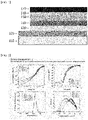
- Fig. 1 is a cross-sectional view of a quantum dot light emitting diode according to one embodiment of the present invention.
- a quantum dot light emitting diode may include a substrate 110, a first electrode 120 and a second electrode 170 that are arranged opposite to each other, a quantum dot light emitting layer 140 that is arranged between the first electrode 120 and the second electrode 170, and an electron transport layer 130 and hole transport layers 150 and 160 that are arranged opposite to each other with respect to the quantum dot light emitting layer 140.
- the electron transport layer 130 may have a monolayer structure composed of an electron injection / transport layer or a bilayer structure composed of an electron injection layer and an electron transport layer.
- the hole transport layers 150 and 160 may have a monolayer structure composed of a hole injection / transport layer or a bilayer structure composed of a hole injection layer and a hole transport layer.
- the substrate 110 supports each layer constituting the quantum dot light emitting diode on the upper portion.
- the substrate 110 may be composed of a transparent material such as glass, quartz, plastic, or organic-inorganic composite polymer having a first refractive index of about 1.4 to about 1.9.
- the substrate 110 may be a glass substrate, and may include borosilicate glass.
- the substrate 110 may be a flexible substrate, and examples thereof may include polyethylene terephthalate (PET), polyethylene naphthalate (PEN), polyethylene (PE), polyethersulfone (PES), polycarbonate (PC), polyarylate (PAR) or polyimide (PI).
- a substrate buffer layer may be arranged on the substrate 110 , but may be omitted depending on the type of substrate and process conditions.
- the substrate buffer layer may be formed of various materials capable of performing the function of flattening a surface while preventing penetration of impurity elements. For example, any one of a silicon nitride (SiN x ) film, a silicon oxide (SiO y ) film, and a silicon oxynitride (SiOxN y ) film may be used as the substrate buffer layer.
- the first electrode 120 may be an anode electrode, and the second electrode 170 may be a cathode electrode, but conversely, the first electrode 120 may be a cathode electrode and the second electrode 170 may be an anode electrode.
- the first electrode 120 and the second electrode 170 may be formed of a transparent conductive material, respectively, or alternatively may be formed of a semi-transmissive or reflective conductive material.
- the first electrode 120 and the second electrode 170 may include indium tin oxide (ITO), indium zinc oxide (IZO), indium zinc tin oxide (IZTO), aluminum zinc oxide (AZO), indium tin oxide-silver-indium tin oxide (ITO-Ag-ITO), indium zinc oxide-silver-indium zinc oxide (IZO-Ag-IZO), indium zinc tin oxide-silver-indium zinc tin oxide (IZTO-Ag-IZTO), aluminum zinc oxide-silver-aluminum zinc oxide (AZO-Ag-AZO), GZO (ZnO-Ga 2 O 3 : zinc oxide doped with gallium), Nb-doped TiO 2 , Ta-doped TiO 2 , and IWZO (In 2 O 3 -WO 3 -ZnO: indium oxide doped with tungsten trioxide and zinc oxide), antimony oxide (Sb 2 O 3 ), zirconium oxide (ZrO 2
- these may include aluminum (Al), gold (Au), silver (Ag), tin (Sn), carbon (C), iron (Fe), cobalt (Co), nickel (Ni), zinc (Zn), tungsten (W), vanadium (V), copper (Cu), iridium (Ir), molybdenum (Mo), palladium (Pd), platinum (Pt), lithium fluoride and aluminum laminate (LiF/Al), calcium and aluminum laminate (Ca/Al) or calcium and silver laminate (Ca/Ag), and the like.
- the light emitting form may provide a top emission, a bottom emission, or a double-sided emission.
- the first electrode 120 is an anode, it may include a material selected from materials having a high work function so as to facilitate hole injection.
- the thickness of the first electrode 120 and the second electrode 170 may be 50 nm to 150 nm.
- the thickness of the first electrode 120 and the second electrode 170 is preferably in the range of 2 nm to 50 nm.
- the light emitting layer 140 may be arranged between the first electrode 120 and the second electrode 170.
- the light emitting layer 140 may include a quantum dot.
- the light emitting layer 140 may include, for example, one or more selected from the group consisting of a red quantum dot having a wavelength of 570 nm to 780 nm in the light emitting region; a green quantum dot having a wavelength of 480 nm to 570 nm in the light emitting region, and a blue quantum dot having a wavelength of 380 to 480 nm in the light emitting region.
- the quantum dot may include a group II-VI compound, a group III-V compound, a group IV-VI compound, a group IV compound, and combinations thereof.
- the group II-VI compound may be selected from the group consisting of a binary compound selected from the group consisting of CdSe, CdTe, ZnS, ZnSe, ZnTe, ZnO, HgS, HgSe, HgTe, MgSe, MgS and mixtures thereof; a ternary compound selected from the group consisting of CdSeS, CdSeTe, CdSTe, ZnSeS, ZnSeTe, ZnSTe, HgSeS, HgSeTe, HgSTe, CdZnS, CdZnSe, CdZnTe, CdHgS, CdHgSe, CdHgTe, HgZnS, HgZnSe, HgZnTe, MgZn
- the group III-V compound may be selected from the group consisting of a binary compound selected from the group consisting of GaN, GaP, GaAs, GaSb, AlN, AlP, AlAs, AlSb, InN, InP, InAs, InSb and mixtures thereof; a ternary compound selected from the group consisting of GaNP, GaNAs, GaNSb, GaPAs, GaPSb, AlNP, AlNAs, AINSb, AlPAs, AlPSb, InNP, InNAs, InNSb, InPAs, InPSb, GaAlNP and mixtures thereof; and a quaternary compound selected from the group consisting of GaAlNAs, GaAlNSb, GaAlPAs, GaAlPSb, GaInNP, GaInNAs, GaInNSb, GaInPAs, GaInPSb, InAlNP, InAlNAs, InAlNSb, InAlPAs, InAlPSb and mixtures thereof.
- the group III-V compound may be selected from the group consisting of a binary compound selected from the group consisting of GaN, GaP, GaAs, GaSb, AlN, AlP, AlAs, AlSb, InN, InP, InAs, InSb and mixtures thereof; a ternary compound selected from the group consisting of GaNP, GaNAs, GaNSb, GaPAs, GaPSb, AlNP, AlNAs, AINSb, AlPAs, AlPSb, InNP, InNAs, InNSb, InPAs, InPSb, GaAlNP InSb and mixtures thereof; and a quaternary compound selected from the group consisting of GaAlNAs, GaAlNSb, GaAlPAs, GaAlPSb, GaInNP, GaInNAs, GaInNSb, GaInPAs, GaInPSb, InAlNP, InAlNAs, InAlNSb, InAlPAs, InAlPSb and mixtures thereof.
- the group IV-VI compound may be selected from the group consisting of a binary compound selected from the group consisting of SnS, SnSe, SnTe, PbS, PbSe, PbTe and mixtures thereof; a ternary compound selected from the group consisting of SnSeS, SnSeTe, SnSTe, PbSeS, PbSeTe, PbSTe, SnPbS, SnPbSe, SnPbTe and mixtures thereof; and a quaternary compound selected from the group consisting of SnPbSSe, SnPbSeTe, SnPbSTe and mixtures thereof.
- the group IV element may be selected from the group consisting of Si, Ge, and mixtures thereof, and the group IV compound may be a binary compound selected from the group consisting of SiC, SiGe, and mixtures thereof.
- group II oxides; group III oxides; group VI oxides; group V oxides; group VI oxides can be included.
- the average particle diameter of the core among the core / shell quantum dots may be 2 nm to 5 nm.
- the average thickness of the shell may be 3 nm to 5 nm.
- the average particle diameter of the quantum dots may be 5 nm to 10 nm.
- the form of the quantum dot is not particularly limited to those generally used in the art, but more specifically, it is preferable to use the form of spherical, pyramidal, multi-arm, or cubic nanoparticles, nanotubes, nanowires, nanofibers, nanoplate particles, and the like.
- the quantum dot may further include a ligand that is formed on the surface of the shell and chemically bound.
- the ligand may include an organic functional group, and the organic functional group may include, for example, oleate, trioctylphosphine, dendrimers, and the like.
- the hole transport layer 150 can be arranged so as to be laminated on the hole injection layer 160.
- the hole transport layer 150 can perform the function of smoothly transporting holes transmitted from the hole injection layer 160.
- the hole transport layer 150 may include HAT-CN (hexaazatriphenylene hexacarbonitrile), molybdenum oxide (MoO 3 ), tungsten oxide (WO 3 ), vanadium pentoxide (V 2 O 5 ), NPD (N,N-dinaphthyl-N,N'-diphenyl benzidine).
- the present invention it has been described as forming a structure in which the hole injection layer 160 and the hole transport layer 150 are laminated, but the present invention is not limited thereto.
- the hole injection layer 160 and the hole transport layer 150 may be formed as a single layer.
- the electron transport layer 130 may include at least one composition selected from the group consisting of In 2 O 3 -ZnO-SiO 2 (In-Zn-Si-O) system, In 2 O 3 -ZnO(In-Zn-O) system, ZnO-SiO 2 (Zn-Si-O) system, In 2 O 3 -SiO 2 (In-Si-O) system, In 2 O 3 -SnO 2 -SiO 2 (In-Sn-Si-O) system, In 2 O 3 -SnO 2 (In-Sn-O) system, SnO 2 -SiO 2 (Sn-Si-O) system, ZnO-SnO 2 -SiO 2 (Zn-Sn-Si-O) system, and ZnO-SnO 2 (Zn-Si-O) system.
- the electron transport layer 130 may be a thin film composed of In-Zn-Si-O (IZSO), In-Zn-
- the metal oxide thin film of the electron transport layer 130 may have the composition of the following chemical formula 2.
- the electron transport layer 130 may be formed by a sputtering method.
- the light emitting layer 140 is prepared as a QLED including quantum dots, but the embodiment is not limited thereto. It can be applied to OLED, printing OLED, printing QLED, flexible OLED, flexible QLED, and the like.
- the first electrode 120 may be formed on the substrate 110 by a sputtering method.
- the electron transport layer 130 may be formed on the first electrode 120 by a sputtering method. That is, both the first electrode 120 and the electron transport layer 130 may be formed by a continuous vapor deposition process through a sputtering method.
- the composition ratio of SiO 2 included in the metal oxide thin film of the electron transport layer 130 can be easily adjusted.
- the electrical conductivity of the electron transport layer 130 may be adjusted by adjusting the SiO 2 content.
- the work function, electron affinity, energy band gap (Eg), Fermi level, and the like can be adjusted by adjusting the SiO 2 content.
- adjusting electron affinity means adjusting the conduction band minimum (CBM) level.
- the temperature of the sputtering process may be room temperature to 400°C.
- the electron transport layer 130 may be sufficiently formed even through a sputtering process at room temperature. Therefore, an electrode and an electron transport layer can be easily formed on a flexible substrate that is vulnerable to heat, and a flexible quantum dot light emitting diode can be provided.
- the sputtering process may be carried out under Ar and O 2 atmospheres.
- Ar:O 2 may be adjusted to 100:1 to 1000:1.
- the battery conductivity of the electron transport layer 130 can also be adjusted by adjusting such oxygen partial pressure. That is, the mobility, carrier concentration, and Fermi level can be adjusted by adjusting the oxygen partial pressure.
- the electron density, electron mobility, electrical conductivity and work function can be easily adjusted as compared with the solution type ZnO layer which is a conventional electron transport layer, so that the efficiency of the quantum dot light emitting layer can be improved.
- the uniformity, reproducibility, and stability of the electron transport layer can be enhanced compared to a conventional solution process.
- the electron transport layer can be formed by a low temperature process, it is applicable to printing OLED, QLED, flexible OLED, flexible QLED, and the like using Soluble.
- the present invention has an effect of reducing exciton quenching due to the dangling bond between the quantum dot and the electron transport layer.
- the surface of the electron transport layer is relatively rough and there is a difference in the size of the contact interface with the quantum dots.
- the metal oxide thin film according to the present invention has an effect of reducing the contact surface area, and based on this, it has an effect of reducing exciton quenching.
- An RF-magnetron sputtering device was used, and an In-Zn-O target and/or an In-Sn-O target having a diameter of 2 inches, and a SiO 2 target were used.
- the position of the gun was designed so as to be adjustable according to the process, and the distance between the target and the substrate was designed to be adjustable according to the mean free path of the target.
- the substrate holder was designed in a structure that can adjust a rotational speed.
- the chamber was composed of a main chamber where sputtering process was carried out and an auxiliary chamber for easily mounting the specimen.
- the highest achieved vacuum degree of the device was 3X10 - 7 Torr, and the high vacuum was measured using an ion gauge. Further, according to the process pressure, a Pirani gauge and a Hot Cathode gauge were used.
- the exhaust system used a rotary pump with a capacity of 550L/min and 150L/min, and a Turbo Molecular Pump (TMP) with an exhaust capacity of 850L/min.
- TMP Turbo Molecular Pump
- Magnet used a circular permanent magnet of 10000 Gauss. A magnetic field was formed by the N and S poles of the central magnet and the outer magnet, and the uniformity of the thin film was maintained.
- the power supply used a high frequency of 13.56 MHz, enabling it to output power up to 300 W.
- the used matching box minimized the reflected waves generated from sputtering, thereby enable transmission of a constant frequency.
- the flow rate of the reaction gas used MFC Mass Flow Controller, Mounting a type 2179 MFC
- the film formation temperature (that is, the substrate temperature) is room temperature.
- Table 1 shows the results of measuring the characteristics of the IZSO electron transport layer due to the change in SiO 2 .
- Mobility [cm 2 /V ⁇ s] carrier concentration [/cm 3 ] Resistivity [ ⁇ cm] Work function [eV] Energy bandgap [eV] 3.05% 2.2E+1 9.8E+19 3.0E-3 4.04 3.74 7.41% 1.4E+1 4.6E+19 9.7E-3 4.01 4.14 15.54% 8.5E+0 1.4E+15 5.2E+2 3.95 4.38 23.62% 3.3E+2 2.1E+12 9.2E+3 3.91 4.75 28.82% 5.6E+2 2.8E+11 3.9E+4 3.89 4.80
- the mobility, carrier concentration, resistivity, work function, energy bandgap, and the like of the electron transport layer change with the change of SiO 2 . That is, it can be seen that the conductivity of the electron transport layer can be adjusted.
- the characteristics of the electron transport layer required in the quantum dot light emitting diode are satisfied in the range of 3% to 29% of SiO 2 . Further, in the previous device application experiment, IZSO 2 (Si 15.75 at%) showed high efficiency.
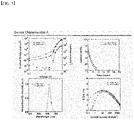
- the IZSO was vacuum deposited so that the resistivity was the highest, and using this, an inverted structured QLED was fabricated.
- a control group (Ref) ZnO was solution-deposited and QLED used as an electron transport layer was used.
- IZSO 1 (10 nm), IZSO 1 (20 nm), IZSO 2 (10 nm), and IZSO 2 (20 nm) all have lower turn-on voltage and higher EQE than the control group (Ref). This can lower the driving current and thereby reduce the power consumption, and maximize the luminous efficiency due to the increase in EQE.
- IZSO 1 having a composition of Si 15.54 at% and IZSO 2 having a composition of Si 15.75 at% were vacuum deposited at 40 nm and 60 nm, respectively, to fabricate an inverse structured QLEDs, and then a characteristic analysis was carried out.
- EQE decreased than the result of Fig. 2 .
- it shows a phenomenon that the driving current is higher than that of the control group (ref).
- Table 2 shows the results of measuring the characteristics of the IZSO electron transport layer according to the oxygen partial pressure.
- Mobility [cm 2 /V ⁇ s] Carrier concentration [/cm 3 ] Resistivity [ ⁇ cm] 1000:1 3.5E+0 2.8E+19 6.3E-2 800:1 1.7E+0 1.0E+18 3.6E+0 500:1 5.9E+0 1.6E+16 6.6E+1 250:1 3.7E+2 2.1E+11 8.0E+4
- the mobility, carrier concentration, and resistivity of the electron transport layer could be adjusted by adjusting the oxygen partial pressure. That is, it can be seen that the conductivity of the electron transport layer can be adjusted by adjusting the oxygen partial pressure.
- Fig. 4 the device characteristics according to the oxygen partial pressure of IZSO (Si 10.05 at%) were evaluated.
- ITSO satisfies the characteristics of the electron transport layer required in the quantum dot light emitting diode in the range of 14% to 54% of SiO 2 .
- Table 4 shows the results of measuring the characteristics of the ITSO electron transport layer according to the oxygen partial pressure.
- the mobility, carrier concentration, and resistivity of the electron transport layer could be adjusted by adjusting the oxygen partial pressure. That is, it can be seen that the conductivity of the electron transport layer can be adjusted by adjusting the oxygen partial pressure.
Abstract
Description
- Various embodiments of the present invention relate to a light emitting diode and a method for producing the same.
- Quantum dots are colloidal semiconductor crystals, which have a size of several nanometers to several tens of nanometers, and have high color purity, color reproducibility, and photostability, and thus are spotlighted as a next-generation light emitting material. By adjusting the particle size of the semiconductor crystal, a wide range of emission wavelengths can be adjusted and the solution process can be applied, whereby there is an advantage that the manufacturing process is simple. For this reason, a quantum dot light emitting diode (QLED) using quantum dots as a light emitting material is being actively studied as a next-generation device.
- A typical quantum dot light emitting diode has an anode electrode, a cathode electrode, and a quantum dot light emitting layer arranged between these electrodes. When a voltage is applied between the electrodes, electrons are injected into the quantum dot light emitting layer from the cathode electrode, and holes are injected into the quantum dot light emitting layer from the anode electrode. A binding energy is generated when holes and electrons are recombined in the quantum dot light emitting layer.
- In general, a metal oxide thin film is used as an electron transport layer in a quantum dot light emitting diode. In one example, a solution type ZnO layer (e.g., a nanoparticle layer or a sol-gel thin film layer) is used as the metal oxide thin film. However, the solution type ZnO layer has a rough surface, which is disadvantageous for uniform light emitting characteristics. Further, such solution type ZnO layer is a major factor of causing an exciton quenching by ligand & dangling-bond of quantum dots, which are inorganic semiconductors.
- Therefore, there is a demand for a electron transport layer based on a vacuum deposition that can overcome the limitations to the use of a solution type ZnO layer.
- Various embodiments of the present invention provide a light emitting diode including an electron transport layer formed by a sputtering method, and a method for producing the same.
- Various embodiments of the present invention can overcome the limitations of existing solution type ZnO layers.
- According to various embodiments of the present invention, there is provided a light emitting diode comprising: a first electrode and a second electrode that are opposite to each other; a light emitting layer that is located between the first electrode and the second electrode and includes a quantum dot; and an electron transport layer that is arranged between the first electrode and the light emitting layer and includes a metal oxide thin film, wherein the metal oxide thin film has a composition including at least one selected from the group consisting of In2O3, ZnO, SiO2 and SnO2.
- According to the present invention, an electrode and an electron transport layer can be manufactured through a sputtering method, and a continuous vapor deposition process can be introduced.
- According to the present invention, an electrode and an electron transport layer can be formed by a vacuum deposition at a low temperature, and thus can be easily applied to a flexible device.
- According to the present invention, a quantum dot light emitting diode having excellent uniformity, reproducibility and stability can be produced in a large quantity.
- According to the present invention, it is easier to adjust the electron density, electron mobility, electrical conductivity and work function than a solution type ZnO layer, which is a conventional electron transport layer, thereby increasing the efficiency of the quantum dot light emitting layer.
- According to the present invention, it has an effect of reducing the occurrence of exciton quenching due to a dangling bond between the quantum dot and the electron transport layer.
-
-
Fig. 1 is a cross-sectional view of a quantum dot light emitting diode according to one embodiment of the present invention; -
Fig. 2 is a graph of measuring characteristics of a quantum dot light emitting diode according to one embodiment of the present invention; and -
Fig. 3 is a graph of measuring characteristics of a quantum dot light emitting diode according to one embodiment of the present invention. - Hereinafter, various embodiments of the present document will be described with reference to the accompanying drawings. Embodiments and terms used therein are not intended to limit the technology described in this document to specific embodiments, and should be understood to cover various modifications, equivalents, and/or substitutions of the embodiments.
- Below, the embodiments of the present invention will be described in detail with reference to the accompanying drawings.
-
Fig. 1 is a cross-sectional view of a quantum dot light emitting diode according to one embodiment of the present invention. - Referring to
Fig. 1 , a quantum dot light emitting diode according to one embodiment of the present invention may include asubstrate 110, afirst electrode 120 and asecond electrode 170 that are arranged opposite to each other, a quantum dotlight emitting layer 140 that is arranged between thefirst electrode 120 and thesecond electrode 170, and anelectron transport layer 130 andhole transport layers light emitting layer 140. - On the other hand, the
electron transport layer 130 may have a monolayer structure composed of an electron injection / transport layer or a bilayer structure composed of an electron injection layer and an electron transport layer. Similarly, thehole transport layers - The
substrate 110 supports each layer constituting the quantum dot light emitting diode on the upper portion. Thesubstrate 110 may be composed of a transparent material such as glass, quartz, plastic, or organic-inorganic composite polymer having a first refractive index of about 1.4 to about 1.9. For example, thesubstrate 110 may be a glass substrate, and may include borosilicate glass. In another example, thesubstrate 110 may be a flexible substrate, and examples thereof may include polyethylene terephthalate (PET), polyethylene naphthalate (PEN), polyethylene (PE), polyethersulfone (PES), polycarbonate (PC), polyarylate (PAR) or polyimide (PI). Further, a substrate buffer layer may be arranged on thesubstrate 110 , but may be omitted depending on the type of substrate and process conditions. The substrate buffer layer may be formed of various materials capable of performing the function of flattening a surface while preventing penetration of impurity elements. For example, any one of a silicon nitride (SiNx) film, a silicon oxide (SiOy) film, and a silicon oxynitride (SiOxNy) film may be used as the substrate buffer layer. - The
first electrode 120 may be an anode electrode, and thesecond electrode 170 may be a cathode electrode, but conversely, thefirst electrode 120 may be a cathode electrode and thesecond electrode 170 may be an anode electrode. Thefirst electrode 120 and thesecond electrode 170 may be formed of a transparent conductive material, respectively, or alternatively may be formed of a semi-transmissive or reflective conductive material. - For example, the
first electrode 120 and thesecond electrode 170 may include indium tin oxide (ITO), indium zinc oxide (IZO), indium zinc tin oxide (IZTO), aluminum zinc oxide (AZO), indium tin oxide-silver-indium tin oxide (ITO-Ag-ITO), indium zinc oxide-silver-indium zinc oxide (IZO-Ag-IZO), indium zinc tin oxide-silver-indium zinc tin oxide (IZTO-Ag-IZTO), aluminum zinc oxide-silver-aluminum zinc oxide (AZO-Ag-AZO), GZO (ZnO-Ga2O3: zinc oxide doped with gallium), Nb-doped TiO2, Ta-doped TiO2, and IWZO (In2O3-WO3-ZnO: indium oxide doped with tungsten trioxide and zinc oxide), antimony oxide (Sb2O3), zirconium oxide (ZrO2), tin oxide (SnO2), and the like, respectively. - Alternatively, these may include aluminum (Al), gold (Au), silver (Ag), tin (Sn), carbon (C), iron (Fe), cobalt (Co), nickel (Ni), zinc (Zn), tungsten (W), vanadium (V), copper (Cu), iridium (Ir), molybdenum (Mo), palladium (Pd), platinum (Pt), lithium fluoride and aluminum laminate (LiF/Al), calcium and aluminum laminate (Ca/Al) or calcium and silver laminate (Ca/Ag), and the like.
- Depending on the type of material that forms the
first electrode 120 and thesecond electrode 170, the light emitting form may provide a top emission, a bottom emission, or a double-sided emission. When thefirst electrode 120 is an anode, it may include a material selected from materials having a high work function so as to facilitate hole injection. - The thickness of the
first electrode 120 and thesecond electrode 170 may be 50 nm to 150 nm. When a metal material is used as the transparent electrode, the thickness of thefirst electrode 120 and thesecond electrode 170 is preferably in the range of 2 nm to 50 nm. - The
light emitting layer 140 may be arranged between thefirst electrode 120 and thesecond electrode 170. Thelight emitting layer 140 may include a quantum dot. Thelight emitting layer 140 may include, for example, one or more selected from the group consisting of a red quantum dot having a wavelength of 570 nm to 780 nm in the light emitting region; a green quantum dot having a wavelength of 480 nm to 570 nm in the light emitting region, and a blue quantum dot having a wavelength of 380 to 480 nm in the light emitting region. - The quantum dot may include a group II-VI compound, a group III-V compound, a group IV-VI compound, a group IV compound, and combinations thereof. The group II-VI compound may be selected from the group consisting of a binary compound selected from the group consisting of CdSe, CdTe, ZnS, ZnSe, ZnTe, ZnO, HgS, HgSe, HgTe, MgSe, MgS and mixtures thereof; a ternary compound selected from the group consisting of CdSeS, CdSeTe, CdSTe, ZnSeS, ZnSeTe, ZnSTe, HgSeS, HgSeTe, HgSTe, CdZnS, CdZnSe, CdZnTe, CdHgS, CdHgSe, CdHgTe, HgZnS, HgZnSe, HgZnTe, MgZnSe, MgZnS and mixtures thereof; and a quaternary compound selected from the group consisting of HgZnTeS, CdZnSeS, CdZnSeTe, CdZnSTe, CdHgSeS, CdHgSeTe, CdHgSTe, HgZnSeS, HgZnSeTe, HgZnSTe and mixtures thereof.
- The group III-V compound may be selected from the group consisting of a binary compound selected from the group consisting of GaN, GaP, GaAs, GaSb, AlN, AlP, AlAs, AlSb, InN, InP, InAs, InSb and mixtures thereof; a ternary compound selected from the group consisting of GaNP, GaNAs, GaNSb, GaPAs, GaPSb, AlNP, AlNAs, AINSb, AlPAs, AlPSb, InNP, InNAs, InNSb, InPAs, InPSb, GaAlNP and mixtures thereof; and a quaternary compound selected from the group consisting of GaAlNAs, GaAlNSb, GaAlPAs, GaAlPSb, GaInNP, GaInNAs, GaInNSb, GaInPAs, GaInPSb, InAlNP, InAlNAs, InAlNSb, InAlPAs, InAlPSb and mixtures thereof.
- The group III-V compound may be selected from the group consisting of a binary compound selected from the group consisting of GaN, GaP, GaAs, GaSb, AlN, AlP, AlAs, AlSb, InN, InP, InAs, InSb and mixtures thereof; a ternary compound selected from the group consisting of GaNP, GaNAs, GaNSb, GaPAs, GaPSb, AlNP, AlNAs, AINSb, AlPAs, AlPSb, InNP, InNAs, InNSb, InPAs, InPSb, GaAlNP InSb and mixtures thereof; and a quaternary compound selected from the group consisting of GaAlNAs, GaAlNSb, GaAlPAs, GaAlPSb, GaInNP, GaInNAs, GaInNSb, GaInPAs, GaInPSb, InAlNP, InAlNAs, InAlNSb, InAlPAs, InAlPSb and mixtures thereof.
- The group IV-VI compound may be selected from the group consisting of a binary compound selected from the group consisting of SnS, SnSe, SnTe, PbS, PbSe, PbTe and mixtures thereof; a ternary compound selected from the group consisting of SnSeS, SnSeTe, SnSTe, PbSeS, PbSeTe, PbSTe, SnPbS, SnPbSe, SnPbTe and mixtures thereof; and a quaternary compound selected from the group consisting of SnPbSSe, SnPbSeTe, SnPbSTe and mixtures thereof.
- The group IV element may be selected from the group consisting of Si, Ge, and mixtures thereof, and the group IV compound may be a binary compound selected from the group consisting of SiC, SiGe, and mixtures thereof. In addition, group II oxides; group III oxides; group VI oxides; group V oxides; group VI oxides can be included.
- The average particle diameter of the core among the core / shell quantum dots may be 2 nm to 5 nm. On the other hand, the average thickness of the shell may be 3 nm to 5 nm. Further, the average particle diameter of the quantum dots may be 5 nm to 10 nm. When the core, shell and quantum dot satisfy the average particle diameter or average thickness range as described above, not only it can behave like a quantum dot, but also it can have excellent dispersibility. By variously selecting the particle diameter of the core, the average thickness of the shell, and the average particle diameter of the quantum dot within the range as described above, the emission color of the quantum dot and/or the semiconductor characteristics of the quantum dot can be variously changed. The form of the quantum dot is not particularly limited to those generally used in the art, but more specifically, it is preferable to use the form of spherical, pyramidal, multi-arm, or cubic nanoparticles, nanotubes, nanowires, nanofibers, nanoplate particles, and the like. In addition, the quantum dot may further include a ligand that is formed on the surface of the shell and chemically bound. The ligand may include an organic functional group, and the organic functional group may include, for example, oleate, trioctylphosphine, dendrimers, and the like.
- On the other hand, the
hole transport layer 150 and thehole injection layer 160 can be arranged on thelight emitting layer 140. Thehole injection layer 160 can play a role in improving the injection of holes from theelectrode 170 into thehole transport layer 150. Thehole injection layer 160 can play a role in improving the injection of holes from theelectrode 170 into thehole transport layer 150. Thehole injection layer 160 can be formed of materials such as CBP (4,4'-Bis(N-carbazolyl)-1,1'-biphenyl), TCTA (Tris(4-carbazoyl-9-ylphenyl)amine), PVK (Poly(9-vinylcarbazole)), TFB (poly(9,9-dioctylfluorene-co-N-(4-butylphenyl)diphenylamine)), CuPc (copper phthalocyanine), PEDOT (poly(3,4)-ethylenedioxythiophene), PANI (polyaniline), NPD (N,N-dinaphthyl-N,N'-diphenyl benzidine) or the like, but is not limited thereto. - The
hole transport layer 150 can be arranged so as to be laminated on thehole injection layer 160. Thehole transport layer 150 can perform the function of smoothly transporting holes transmitted from thehole injection layer 160. Thehole transport layer 150 may include HAT-CN (hexaazatriphenylene hexacarbonitrile), molybdenum oxide (MoO3), tungsten oxide (WO3), vanadium pentoxide (V2O5), NPD (N,N-dinaphthyl-N,N'-diphenyl benzidine). (N,N'-bis-(3-methylphenyl)-N,N'-bis(phenyl)-benzidine), s-TAD, MTDATA (4,4',4 "-tris(N-3-methylphenyl-Nphenyl))-amino)-triphenylamine), TCTA (4-(9H-carbazol-9-yl)-N,N-bis[4-(9H-carbazol-9-yl)phenyl]-benzidine), CBP (4,4'-N,N'-dicarbazole-biphenyl), and the like. but is not limited thereto. - In the present invention, it has been described as forming a structure in which the
hole injection layer 160 and thehole transport layer 150 are laminated, but the present invention is not limited thereto. Thehole injection layer 160 and thehole transport layer 150 may be formed as a single layer. - An
electron transport layer 130 may be arranged between thefirst electrode 120 and theemission layer 140. Theelectron transport layer 130 according to the present invention may include a metal oxide thin film. At this time, theelectron transport layer 130 may have a composition including at least one selected from the group consisting of In2O3, ZnO, SiO2 and SnO2. Theelectron transport layer 130 may be amorphous, crystalline, or a mixed phase of amorphous and crystalline. Specifically, theelectron transport layer 130 may include at least one composition selected from the group consisting of In2O3-ZnO-SiO2 (In-Zn-Si-O) system, In2O3-ZnO(In-Zn-O) system, ZnO-SiO2 (Zn-Si-O) system, In2O3-SiO2 (In-Si-O) system, In2O3-SnO2-SiO2 (In-Sn-Si-O) system, In2O3-SnO2 (In-Sn-O) system, SnO2-SiO2 (Sn-Si-O) system, ZnO-SnO2-SiO2 (Zn-Sn-Si-O) system, and ZnO-SnO2 (Zn-Si-O) system. Preferably, theelectron transport layer 130 may be a thin film composed of In-Zn-Si-O (IZSO), In-Sn-Si-O (ITSO), or Zn-Sn-Si-O (ZTSO). - Specifically, the metal oxide thin film of the
electron transport layer 130 may have a composition represented by the followingchemical formula 1.
[Chemical Formula 1] (1-y)[(1-x)(In2O3)-xZnO]-ySiO2
wherein, inchemical formula - Alternatively, the metal oxide thin film of the
electron transport layer 130 may have the composition of the followingchemical formula 2.
[Chemical Formula 2] (1-y)[(1-x)(In2O3)-xSnO2]-ySiO2
wherein, inchemical formula - Alternatively, the metal oxide thin film of the
electron transport layer 130 may have the composition of the followingchemical formula 3.
[Chemical Formula 3] (1-y)[(1-x)(ZnO)-xSnO2]-ySiO2
wherein, inchemical formula - On the other hand, the thickness of such an
electron transport layer 130 can be 10 nm to 100 nm. - The
electron transport layer 130 may be formed by a sputtering method. - On the other hand, in the present invention, the
light emitting layer 140 is prepared as a QLED including quantum dots, but the embodiment is not limited thereto. It can be applied to OLED, printing OLED, printing QLED, flexible OLED, flexible QLED, and the like. - Below, a method of manufacturing the quantum dot light emitting diode including the
electron transport layer 130 will be described in more detail. - First, the
first electrode 120 may be formed on thesubstrate 110 by a sputtering method. - Next, the
electron transport layer 130 may be formed on thefirst electrode 120 by a sputtering method. That is, both thefirst electrode 120 and theelectron transport layer 130 may be formed by a continuous vapor deposition process through a sputtering method. - In the step of forming the
electron transport layer 130, it can be carried out by a sputtering method using an In-Zn-O target and a SiO2 target. Alternatively, it can be carried out by the sputtering method using an In-Sn-O target and a SiO2 target. Alternatively, it can be carried out by a sputtering method using a Zn-Sn-O target and a SiO2 target. - In the present invention, by separately using the SiO2 target, the composition ratio of SiO2 included in the metal oxide thin film of the
electron transport layer 130 can be easily adjusted. The electrical conductivity of theelectron transport layer 130 may be adjusted by adjusting the SiO2 content. In addition, the work function, electron affinity, energy band gap (Eg), Fermi level, and the like can be adjusted by adjusting the SiO2 content. Here, adjusting electron affinity means adjusting the conduction band minimum (CBM) level. - However, the embodiment is not limited thereto, and it may be carried out by a single target sputtering method using any one target selected from the group consisting of an In-Zn-Si-O target, an In-Sn-Si-O target, and a Zn-Sn-Si-O target.
- In this case, the temperature of the sputtering process may be room temperature to 400°C. According to the present invention, the
electron transport layer 130 may be sufficiently formed even through a sputtering process at room temperature. Therefore, an electrode and an electron transport layer can be easily formed on a flexible substrate that is vulnerable to heat, and a flexible quantum dot light emitting diode can be provided. - In addition, the sputtering process may be carried out under Ar and O2 atmospheres. At this time, Ar:O2 may be adjusted to 100:1 to 1000:1. The battery conductivity of the
electron transport layer 130 can also be adjusted by adjusting such oxygen partial pressure. That is, the mobility, carrier concentration, and Fermi level can be adjusted by adjusting the oxygen partial pressure. - In the case of a quantum dot light emitting diode, in the
light emitting layer 140, the n-type has a stronger characteristic than the p-type, and the charge transport characteristic of the electron transport layer does not need to be excessively excellent. Therefore, in order to reduce the interfacial exciton quenching, it is necessary to adjust the electrical conductivity (conductivity = mobility ∗ carrier concentration) of theelectron transport layer 130 to be small. - According to the present invention, the electron density, electron mobility, electrical conductivity and work function can be easily adjusted as compared with the solution type ZnO layer which is a conventional electron transport layer, so that the efficiency of the quantum dot light emitting layer can be improved. In addition, the uniformity, reproducibility, and stability of the electron transport layer can be enhanced compared to a conventional solution process. Further, since the electron transport layer can be formed by a low temperature process, it is applicable to printing OLED, QLED, flexible OLED, flexible QLED, and the like using Soluble.
- Further, according to the present invention, it has an effect of reducing exciton quenching due to the dangling bond between the quantum dot and the electron transport layer. In the case of an electron transport layer using conventional solution type ZnO or ZnO nanopowder, the surface of the electron transport layer is relatively rough and there is a difference in the size of the contact interface with the quantum dots. However, the metal oxide thin film according to the present invention has an effect of reducing the contact surface area, and based on this, it has an effect of reducing exciton quenching.
- Hereinafter, the present invention will be described in more detail with reference to the following examples. However, these examples are only for illustrating the present invention, and the present invention is not limited thereto.
- An RF-magnetron sputtering device was used, and an In-Zn-O target and/or an In-Sn-O target having a diameter of 2 inches, and a SiO2 target were used. The position of the gun was designed so as to be adjustable according to the process, and the distance between the target and the substrate was designed to be adjustable according to the mean free path of the target. In order to produce a uniform film, the substrate holder was designed in a structure that can adjust a rotational speed.
- Further, in order not to affect the board during pre-sputtering, it was double-designed with a gun shutter and a main shutter. The chamber was composed of a main chamber where sputtering process was carried out and an auxiliary chamber for easily mounting the specimen.
- The highest achieved vacuum degree of the device was 3X10⁻⁷ Torr, and the high vacuum was measured using an ion gauge. Further, according to the process pressure, a Pirani gauge and a Hot Cathode gauge were used. The exhaust system used a rotary pump with a capacity of 550L/min and 150L/min, and a Turbo Molecular Pump (TMP) with an exhaust capacity of 850L/min. Magnet used a circular permanent magnet of 10000 Gauss. A magnetic field was formed by the N and S poles of the central magnet and the outer magnet, and the uniformity of the thin film was maintained.
- The power supply used a high frequency of 13.56 MHz, enabling it to output power up to 300 W. The used matching box minimized the reflected waves generated from sputtering, thereby enable transmission of a constant frequency.
- In the sputtering process using plasma, a large amount of energy is generally transferred to the target during the vapor deposition process, and the target temperature rises. When the temperature rises, it causes deterioration of the magnet, and particles with high energy collide with the thin film to cause damage, and the life of the sputter is shortened. In order to solve these problems, a water-cooled cooling device was constructed under the holder in the present experiment.
- The flow rate of the reaction gas used MFC (Mass Flow Controller, Mounting a type 2179 MFC), and as the reaction gas, Ar (99.99%), O2 (99.99%), and a mixed gas of Ar and O2 (Ar:O2=1000:1, 99.99%) were used. The film formation temperature (that is, the substrate temperature) is room temperature.
- Through the sputtering process under these process conditions, it was succeeded in forming an electron transport layer containing metal oxide thin film having a composition of (1-y)[(1-x)(In2O3)-xZnO]-ySiO2 where x = 0.75, and y = 15.54,
- In order to compare the characteristics of each IZSO composition according to the SiO2 content in IZSO (In-Zn-Si-O), co-sputtering was carried out using an In-Zn-O target and a SiO2 target. First, it was set to oxygen partial pressure(O2/(Ar+O2)) = 0.001%, working pressure = 10 mTorr, Substrate Temperature = Room Temperature, and thin film deposition was carried out by adjusting the RF power of the In-Zn-O target and the SiO2 target. For comparison of thin film characteristics according to SiO2 content, the substrate holder was fixed and deposition was carried out.
- Table 1 below shows the results of measuring the characteristics of the IZSO electron transport layer due to the change in SiO2.
[Table 1] Mobility [cm2/V·s] carrier concentration [/cm3] Resistivity [Ωcm] Work function [eV] Energy bandgap [eV] 3.05% 2.2E+1 9.8E+19 3.0E-3 4.04 3.74 7.41% 1.4E+1 4.6E+19 9.7E-3 4.01 4.14 15.54% 8.5E+0 1.4E+15 5.2E+2 3.95 4.38 23.62% 3.3E+2 2.1E+12 9.2E+3 3.91 4.75 28.82% 5.6E+2 2.8E+11 3.9E+4 3.89 4.80 - Referring to Table 1 above, it can be seen that the mobility, carrier concentration, resistivity, work function, energy bandgap, and the like of the electron transport layer change with the change of SiO2. That is, it can be seen that the conductivity of the electron transport layer can be adjusted.
- Further, it can be confirmed that the characteristics of the electron transport layer required in the quantum dot light emitting diode are satisfied in the range of 3% to 29% of SiO2. Further, in the previous device application experiment, IZSO2 (Si 15.75 at%) showed high efficiency.
- Referring to
Figs. 2 and3 , the characteristics of QLED according to the composition and deposition thickness of IZSO (In-Zn-Si-O) were observed. InFig. 2 , IZSO 1 (10 nm) is a QLED using an electron transport layer having a deposition thickness of 10 nm and a composition of Si 15.54 at%, IZSO 1 (20 nm) is a QLED using an electron transport layer having a deposition thickness of 10 nm and a composition of Si 15.54 at%, IZSO 2 (10 nm) is a QLED using an electron transport layer having a deposition thickness of 10 nm and a composition of Si 15.75 at%, and IZSO 2 (20 nm) is a QLED using an electron transport layer having a deposition thickness of 20 nm and a composition of Si 15.75 at%. At this time, the IZSO was vacuum deposited so that the resistivity was the highest, and using this, an inverted structured QLED was fabricated. On the other hand, as a control group (Ref), ZnO was solution-deposited and QLED used as an electron transport layer was used. - As a result, it can be seen that IZSO 1 (10 nm), IZSO 1 (20 nm), IZSO 2 (10 nm), and IZSO 2 (20 nm) all have lower turn-on voltage and higher EQE than the control group (Ref). This can lower the driving current and thereby reduce the power consumption, and maximize the luminous efficiency due to the increase in EQE.
- Referring to
Fig. 3 ,IZSO 1 having a composition of Si 15.54 at% andIZSO 2 having a composition of Si 15.75 at% were vacuum deposited at 40 nm and 60 nm, respectively, to fabricate an inverse structured QLEDs, and then a characteristic analysis was carried out. As a result, as the thickness increases, the resistivity decreases and the conductivity increases, so that exciton quenching at the interface becomes more active. Consequently, EQE decreased than the result ofFig. 2 . In addition, it shows a phenomenon that the driving current is higher than that of the control group (ref). - In order to compare the characteristics of the IZSO electron transport layer according to the oxygen partial pressure adjustment (Ar:O2), sputtering was carried out by fixing the SiO2 content (Si 10.05at%).
- Table 2 below shows the results of measuring the characteristics of the IZSO electron transport layer according to the oxygen partial pressure.
[Table 2] Mobility [cm2/V·s] Carrier concentration [/cm3] Resistivity [Ωcm] 1000:1 3.5E+0 2.8E+19 6.3E-2 800:1 1.7E+0 1.0E+18 3.6E+0 500:1 5.9E+0 1.6E+16 6.6E+1 250:1 3.7E+2 2.1E+11 8.0 E+ 4 - Referring to Table 2 above, it was confirmed that the mobility, carrier concentration, and resistivity of the electron transport layer could be adjusted by adjusting the oxygen partial pressure. That is, it can be seen that the conductivity of the electron transport layer can be adjusted by adjusting the oxygen partial pressure.
- Referring to
Fig. 4 , the device characteristics according to the oxygen partial pressure of IZSO (Si 10.05 at%) were evaluated. InFig. 4 , 250:1 is a result of fabricating a QLED in which IZSO (Si 10.05 at%) adjusted to Ar:O2 = 250:1 was applied as an electron transport layer and then a characteristic analysis was carried out. 500:1 is a QLED in which IZSO (Si 10.05 at%) adjusted to Ar:O2 = 250:1 was applied as an electron transport layer, and 1000:1 relates to a QLED in which IZSO (Si 10.05at%) adjusted to Ar:O2 = 1000:1 is applied as an electron transport layer. As a result, the best characteristics were shown at Ar: O2 = 250: 1. That is, as confirmed in Experimental Example 3, the higher the oxygen partial pressure, the lower the carrier concentration. It was confirmed that QLED device characteristics were improved through low carrier concentration. That is, referring toFig. 4 , it can be confirmed that device characteristics are better at 250:1 than at 1000:1 and 500:1 which have relatively high carrier concentration. - In order to compare the characteristics of each ITSO composition according to the SiO2 content in ITSO (In-Sn-Si-O), co-sputtering was carried out using the In-Sn-O target and the SiO2 target. First, it was fixed to oxygen partial pressure (O2/(Ar+O2)) = 0.001%, working pressure = 10 mTorr, and substrate temperature = room temperature, and the thin film deposition was carried out by adjusting the RF power of the In-Sn-O target and the SiO2 target. In order to compare the thin film characteristics according to the SiO2 content, the substrate holder was fixed and vapor-deposited.
- Table 3 below shows the results of measuring the characteristics of the ITSO electron transport layer according to the change in SiO2.
[Table 3] Mobility [cm2/V·s] Carrier concentration [/cm3] Resistivity [Ωcm] Work function [eV] Energy bandgap [eV] 14.9 % 1.7E-1 1.9E+20 1.9E-3 4.41 4.11 29.6 % 1.3E+0 3.0E+17 1.5E+1 4.28 4.45 33.0 % 3.6E+1 1.0E+15 1.6E+2 4.30 4.56 41.1 % 4.9E+2 5.6E+12 2.3E+3 4.24 4.74 53.8 % 7.6E+2 1.4E+12 5.7E+3 4.58 5.19 - Referring to Table 3 above, it can be seen that the mobility, carrier concentration, resistivity, work function, energy bandgap, and the like of the ITSO electron transport layer change with the change of SiO2. That is, it can be seen that the conductivity of the electron transport layer can be adjusted.
- In addition, it can be confirmed that ITSO satisfies the characteristics of the electron transport layer required in the quantum dot light emitting diode in the range of 14% to 54% of SiO2.
- In order to compare the characteristics of the metal oxide thin film according to the oxygen partial pressure control (Ar:O2) of the ITSO thin film, sputtering was carried out by fixing the SiO2 content (Si 33.0 at%).
- Table 4 below shows the results of measuring the characteristics of the ITSO electron transport layer according to the oxygen partial pressure.
[Table 4] Mobility [cm2/V·s] carrier concentration [/cm3] Resistivity [Ωcm] 1000:1 7.9E-1 6.8E+18 1.2E+0 100:1 1.4E+2 1.8E+11 1.1 E+ 0 - Referring to Table 4 above, it was confirmed that the mobility, carrier concentration, and resistivity of the electron transport layer could be adjusted by adjusting the oxygen partial pressure. That is, it can be seen that the conductivity of the electron transport layer can be adjusted by adjusting the oxygen partial pressure.
- Referring to
Fig. 5 , the device characteristics according to the oxygen partial pressure of ITSO (Si 33.0 at%) were evaluated. InFig. 5 , 100:1 is a QLED in which ITSO (Si 33.0 at%) adjusted to Ar:O2 = 100: 1 is applied as an electron transport layer, and 1000:1 relates to a QLED in which ITSO (Si 33.0 at%) adjusted to Ar:O2 = 1000:1 is applied as an electron transport layer. - As a result, Ar:O2 = 100:1 showed better characteristics than 1000: 1. That is, as confirmed in Experimental Example 6, the higher the oxygen partial pressure, the lower the carrier concentration, and it was confirmed that the QLED device characteristics are improved through the lower carrier concentration.
- The features, structures, effects, and the like described in the above embodiments are included in at least one embodiment of the present invention, and are not necessarily limited to only one embodiment. Furthermore, the features, structures, effects, and the like illustrated in each embodiment can be combined or modified with respect to other embodiments by a person having ordinary knowledge in the field to which the embodiment belongs. Therefore, the contents related to such combinations and modifications should be construed as being included in the scope of the present invention.
- In addition, although the embodiments have been mainly described above, this is only an example and does not limit the present invention. Anyone with ordinary knowledge of the field to which the present invention belongs will appreciate that various modifications and applications not exemplified above can be made without departing from the essential characteristics of the present embodiment. For example, each component specifically shown in the embodiments can be modified and implemented. Further, the differences related to such modifications and applications should be construed as being included in the scope of the present invention defined in the appended claims.
Claims (13)
- A light emitting diode comprising:a first electrode and a second electrode that are opposite to each other;a light emitting layer that is located between the first electrode and the second electrode and includes a quantum dot; andan electron transport layer that is arranged between the first electrode and the light emitting layer and includes a metal oxide thin film,wherein the metal oxide thin film has a composition including at least one selected from the group consisting of In2O3, ZnO, SiO2 and SnO2.
- The light emitting diode according to claim 1, wherein:
the metal oxide thin film is formed through a sputtering method. - The light emitting diode according to claim 1, wherein:
the metal oxide thin film includes at least one composition selected from the group consisting of In2O3-ZnO-SiO2 system, In2O3-ZnO system, ZnO-SiO2 system, In2O3-SiO2 system, In2O3-SnO2-SiO2 system, In2O3-SnO2 system, SnO2-SiO2 system, ZnO-SnO2-SiO2 system, and ZnO-SnO2 system. - The light emitting diode according to claim 1, wherein:
the metal oxide thin film has a composition of the following chemical formula 1.
[Chemical Formula 1] (1-y)[(1-x)(In2O3)-xZnO]-ySiO2
wherein, in chemical formula 1, 0≤x≤1 and 0≤y<1. - The light emitting diode according to claim 1, wherein:
the metal oxide thin film has a composition of the following chemical formula 2.
[Chemical Formula 2] (1-y)[(1-x)(In2O3)-xSnO2]-ySiO2
wherein, in chemical formula 2, 0≤x≤1 and 0≤y<1. - The light emitting diode according to claim 1, wherein:
the metal oxide thin film has a composition of the following chemical formula 3.
[Chemical Formula 3] (1-y)[(1-x)(ZnO)-xSnO2]-ySiO2
wherein, in chemical formula 3, 0≤x≤1 and 0≤y<1. - A method for manufacturing a light emitting diode, comprising:a step of forming a first electrode on a substrate; anda step of forming an electron transport layer on the first electrode,wherein the step of forming the electron transport layer is carried out by a sputtering method.
- The method for manufacturing a light emitting diode according to claim 7, wherein:
the step of forming a first electrode and the step of forming an electron transport layer are carried out by a continuous vapor deposition process through the sputtering method. - The method for manufacturing a light emitting diode according to claim 7, wherein:
the step of forming an electron transport layer are carried out by a sputtering method using In-Zn-O target and SiO2 target. - The method for manufacturing a light emitting diode according to claim 7, wherein:
the step of forming an electron transport layer are carried out by a sputtering method using In-Sn-O target and SiO2 target. - The method for manufacturing a light emitting diode according to claim 7, wherein:
the step of forming an electron transport layer are carried out by a sputtering method using In-Zn-O target and SiO2 target. - The method for manufacturing a light emitting diode according to claim 7, wherein:
the method is carried out by a single target sputtering method using any one target selected from the group consisting of an In-Zn-Si-O target, an In-Sn-Si-O target, and a Zn-Sn-Si-O target. - The method for manufacturing a light emitting diode according to claim 7, wherein:
the composition ratio of SiO2 is adjusted through the sputtering method in the step of forming the electron transport layer.
Applications Claiming Priority (2)
| Application Number | Priority Date | Filing Date | Title |
|---|---|---|---|
| KR1020190068913A KR102304839B1 (en) | 2019-06-11 | 2019-06-11 | Electro-luminescence diode and Method of manufacturing for the same |
| PCT/KR2020/007535 WO2020251262A1 (en) | 2019-06-11 | 2020-06-10 | Light-emitting diode, and method for producing same |
Publications (2)
| Publication Number | Publication Date |
|---|---|
| EP3985751A1 true EP3985751A1 (en) | 2022-04-20 |
| EP3985751A4 EP3985751A4 (en) | 2023-02-15 |
Family
ID=73782219
Family Applications (1)
| Application Number | Title | Priority Date | Filing Date |
|---|---|---|---|
| EP20822015.2A Pending EP3985751A4 (en) | 2019-06-11 | 2020-06-10 | Light-emitting diode, and method for producing same |
Country Status (4)
| Country | Link |
|---|---|
| US (1) | US20220278297A1 (en) |
| EP (1) | EP3985751A4 (en) |
| KR (1) | KR102304839B1 (en) |
| WO (1) | WO2020251262A1 (en) |
Family Cites Families (6)
| Publication number | Priority date | Publication date | Assignee | Title |
|---|---|---|---|---|
| US20090039764A1 (en) * | 2005-03-17 | 2009-02-12 | Cho Kyung Sang | Quantum Dot Light-Emitting Diode Comprising Inorganic Electron Transport Layer |
| KR101995369B1 (en) * | 2008-04-03 | 2019-07-02 | 삼성 리서치 아메리카 인코포레이티드 | Light-emitting device including quantum dots |
| CN106687616A (en) * | 2014-09-18 | 2017-05-17 | 国立研究开发法人科学技术振兴机构 | Metal oxide thin film, organic electroluminescent element provided with said thin film, solar cell, and method for producing thin film |
| KR20170102401A (en) * | 2016-03-01 | 2017-09-11 | 박철 | Quantum Dot Light Emitting Device |
| CN108269886B (en) * | 2016-12-30 | 2019-12-10 | Tcl集团股份有限公司 | Quantum dot material, preparation method and semiconductor device |
| KR101975667B1 (en) * | 2017-08-04 | 2019-05-07 | 서울대학교산학협력단 | Light emitting diode |
-
2019
- 2019-06-11 KR KR1020190068913A patent/KR102304839B1/en active IP Right Grant
-
2020
- 2020-06-10 EP EP20822015.2A patent/EP3985751A4/en active Pending
- 2020-06-10 US US17/618,392 patent/US20220278297A1/en active Pending
- 2020-06-10 WO PCT/KR2020/007535 patent/WO2020251262A1/en unknown
Also Published As
| Publication number | Publication date |
|---|---|
| WO2020251262A1 (en) | 2020-12-17 |
| KR102304839B1 (en) | 2021-09-24 |
| US20220278297A1 (en) | 2022-09-01 |
| KR20200141848A (en) | 2020-12-21 |
| EP3985751A4 (en) | 2023-02-15 |
Similar Documents
| Publication | Publication Date | Title |
|---|---|---|
| US9905790B2 (en) | Optoelectronic device including quantum dot | |
| US11818907B2 (en) | Quantum-dot light emitting device comprising solution processed charge generation junction and manufacturing method thereof | |
| EP2221355B1 (en) | Quantum dot light emitting device having quantum dot multilayer | |
| US10446781B2 (en) | Quantum dot device and electronic device | |
| US20080309234A1 (en) | Alternating current driving type quantum dot electroluminescent device | |
| US10818859B2 (en) | Electroluminescent device, and display device comprising thereof | |
| KR20190108389A (en) | Electroluminescent device, and display device comprising thereof | |
| US11812627B2 (en) | Quantum dot device and electronic device | |
| US11139441B2 (en) | Quantum dot device and electronic device comprising an emissive quantum dot and a non-emissive quantum dot | |
| KR102001734B1 (en) | Quantum dot lightemitting device and manufacturing method therefor | |
| US11018311B2 (en) | Device with quantum dot emissive layer and display device comprising the same | |
| KR102618343B1 (en) | Quantum dot light emitting diode device | |
| US20180175132A1 (en) | Organic light emitting diode and organic light emitting display device including the same | |
| KR102110780B1 (en) | Quantum dot light emitting device and the method for manufacturing thereof | |
| KR101980979B1 (en) | Thin-film light emitting device comprising charge electron transport layer and manufacturing method thereof | |
| KR101878615B1 (en) | Quantumdot light emitting diode with enhanced stability and method of fabrication thereof | |
| US20210143355A1 (en) | Thin film electroluminescent device, preparation method thereof, and electronic device | |
| EP3985751A1 (en) | Light-emitting diode, and method for producing same | |
| CN109860427B (en) | Quantum dot light-emitting device and preparation method thereof | |
| KR20080095522A (en) | Organic electroluminescent device and method for fabricating thereof | |
| KR102125204B1 (en) | Thin-film light emitting device comprising charge electron transport layer and manufacturing method thereof | |
| KR20170091818A (en) | Light emitting diode | |
| CN117693220A (en) | Light emitting device, preparation method thereof and light emitting device | |
| CN116156919A (en) | Light-emitting device, preparation method thereof and display device | |
| CN114686231A (en) | Particle, preparation method thereof and quantum dot light-emitting diode |
Legal Events
| Date | Code | Title | Description |
|---|---|---|---|
| STAA | Information on the status of an ep patent application or granted ep patent |
Free format text: STATUS: THE INTERNATIONAL PUBLICATION HAS BEEN MADE |
|
| PUAI | Public reference made under article 153(3) epc to a published international application that has entered the european phase |
Free format text: ORIGINAL CODE: 0009012 |
|
| STAA | Information on the status of an ep patent application or granted ep patent |
Free format text: STATUS: REQUEST FOR EXAMINATION WAS MADE |
|
| 17P | Request for examination filed |
Effective date: 20211222 |
|
| AK | Designated contracting states |
Kind code of ref document: A1 Designated state(s): AL AT BE BG CH CY CZ DE DK EE ES FI FR GB GR HR HU IE IS IT LI LT LU LV MC MK MT NL NO PL PT RO RS SE SI SK SM TR |
|
| DAV | Request for validation of the european patent (deleted) | ||
| DAX | Request for extension of the european patent (deleted) | ||
| REG | Reference to a national code |
Ref country code: DE Ref legal event code: R079 Free format text: PREVIOUS MAIN CLASS: H01L0051500000 Ipc: H10K0050160000 |
|
| A4 | Supplementary search report drawn up and despatched |
Effective date: 20230117 |
|
| RIC1 | Information provided on ipc code assigned before grant |
Ipc: H10K 50/115 20230101ALI20230111BHEP Ipc: H10K 50/16 20230101AFI20230111BHEP |