EP3985715A1 - Design method for wafer layout and lithography machine exposure system - Google Patents
Design method for wafer layout and lithography machine exposure system Download PDFInfo
- Publication number
- EP3985715A1 EP3985715A1 EP21817512.3A EP21817512A EP3985715A1 EP 3985715 A1 EP3985715 A1 EP 3985715A1 EP 21817512 A EP21817512 A EP 21817512A EP 3985715 A1 EP3985715 A1 EP 3985715A1
- Authority
- EP
- European Patent Office
- Prior art keywords
- wafer
- yield
- layout
- die
- center
- Prior art date
- Legal status (The legal status is an assumption and is not a legal conclusion. Google has not performed a legal analysis and makes no representation as to the accuracy of the status listed.)
- Ceased
Links
Images
Classifications
-
- G—PHYSICS
- G03—PHOTOGRAPHY; CINEMATOGRAPHY; ANALOGOUS TECHNIQUES USING WAVES OTHER THAN OPTICAL WAVES; ELECTROGRAPHY; HOLOGRAPHY
- G03F—PHOTOMECHANICAL PRODUCTION OF TEXTURED OR PATTERNED SURFACES, e.g. FOR PRINTING, FOR PROCESSING OF SEMICONDUCTOR DEVICES; MATERIALS THEREFOR; ORIGINALS THEREFOR; APPARATUS SPECIALLY ADAPTED THEREFOR
- G03F7/00—Photomechanical, e.g. photolithographic, production of textured or patterned surfaces, e.g. printing surfaces; Materials therefor, e.g. comprising photoresists; Apparatus specially adapted therefor
- G03F7/70—Microphotolithographic exposure; Apparatus therefor
- G03F7/70425—Imaging strategies, e.g. for increasing throughput or resolution, printing product fields larger than the image field or compensating lithography- or non-lithography errors, e.g. proximity correction, mix-and-match, stitching or double patterning
- G03F7/70433—Layout for increasing efficiency or for compensating imaging errors, e.g. layout of exposure fields for reducing focus errors; Use of mask features for increasing efficiency or for compensating imaging errors
-
- G—PHYSICS
- G03—PHOTOGRAPHY; CINEMATOGRAPHY; ANALOGOUS TECHNIQUES USING WAVES OTHER THAN OPTICAL WAVES; ELECTROGRAPHY; HOLOGRAPHY
- G03F—PHOTOMECHANICAL PRODUCTION OF TEXTURED OR PATTERNED SURFACES, e.g. FOR PRINTING, FOR PROCESSING OF SEMICONDUCTOR DEVICES; MATERIALS THEREFOR; ORIGINALS THEREFOR; APPARATUS SPECIALLY ADAPTED THEREFOR
- G03F7/00—Photomechanical, e.g. photolithographic, production of textured or patterned surfaces, e.g. printing surfaces; Materials therefor, e.g. comprising photoresists; Apparatus specially adapted therefor
- G03F7/20—Exposure; Apparatus therefor
-
- G—PHYSICS
- G06—COMPUTING OR CALCULATING; COUNTING
- G06F—ELECTRIC DIGITAL DATA PROCESSING
- G06F17/00—Digital computing or data processing equipment or methods, specially adapted for specific functions
-
- G—PHYSICS
- G06—COMPUTING OR CALCULATING; COUNTING
- G06F—ELECTRIC DIGITAL DATA PROCESSING
- G06F30/00—Computer-aided design [CAD]
- G06F30/30—Circuit design
- G06F30/39—Circuit design at the physical level
- G06F30/398—Design verification or optimisation, e.g. using design rule check [DRC], layout versus schematics [LVS] or finite element methods [FEM]
-
- H—ELECTRICITY
- H10—SEMICONDUCTOR DEVICES; ELECTRIC SOLID-STATE DEVICES NOT OTHERWISE PROVIDED FOR
- H10P—GENERIC PROCESSES OR APPARATUS FOR THE MANUFACTURE OR TREATMENT OF DEVICES COVERED BY CLASS H10
- H10P74/00—Testing or measuring during manufacture or treatment of wafers, substrates or devices
-
- H—ELECTRICITY
- H10—SEMICONDUCTOR DEVICES; ELECTRIC SOLID-STATE DEVICES NOT OTHERWISE PROVIDED FOR
- H10P—GENERIC PROCESSES OR APPARATUS FOR THE MANUFACTURE OR TREATMENT OF DEVICES COVERED BY CLASS H10
- H10P95/00—Generic processes or apparatus for manufacture or treatments not covered by the other groups of this subclass
-
- G—PHYSICS
- G06—COMPUTING OR CALCULATING; COUNTING
- G06F—ELECTRIC DIGITAL DATA PROCESSING
- G06F2119/00—Details relating to the type or aim of the analysis or the optimisation
- G06F2119/22—Yield analysis or yield optimisation
-
- G—PHYSICS
- G06—COMPUTING OR CALCULATING; COUNTING
- G06F—ELECTRIC DIGITAL DATA PROCESSING
- G06F30/00—Computer-aided design [CAD]
- G06F30/30—Circuit design
- G06F30/39—Circuit design at the physical level
- G06F30/392—Floor-planning or layout, e.g. partitioning or placement
-
- H—ELECTRICITY
- H10—SEMICONDUCTOR DEVICES; ELECTRIC SOLID-STATE DEVICES NOT OTHERWISE PROVIDED FOR
- H10D—INORGANIC ELECTRIC SEMICONDUCTOR DEVICES
- H10D89/00—Aspects of integrated devices not covered by groups H10D84/00 - H10D88/00
- H10D89/10—Integrated device layouts
Definitions
- Embodiments of the present application relate to the technical field of semiconductor, and in particular to a design method of a wafer layout and an exposure system of a lithography machine.
- Semiconductor wafers such as wafers made of silicon, germanium, and III-V materials are used in the manufacture of integrated circuits.
- Various semiconductor processes such as lithography (e.g. patterning, etching, and deposition), epitaxial growth, doping, polishing, and other such processes, may be used on wafers to form dies.
- lithography e.g. patterning, etching, and deposition
- epitaxial growth e.g. patterning, etching, and deposition
- a wafer layout may be calculated according to a die size, an arrangement mode of dies in a single shot, and a wafer edge cleaning position, so that a maximum number of complete dies are obtained within the wafer edge cleaning position.
- the inventors have found that since the yield of dies in the radial distribution of wafers is not all 100% in actual production, the number of qualified dies on a single wafer during the production of a wafer layout in the prior art is often smaller than the number of calculated complete dies, so that the yield of the single wafer is low.
- Some embodiments of the present application aim at providing a design method of a wafer layout and an exposure system of a lithography machine. A large number of qualified dies are obtained during the production of a wafer layout obtained according to the design method of a wafer layout.
- the embodiments of the present application provide a design method of a wafer layout, which may include: providing a yield distribution map of a wafer under an initial wafer layout; determining a yield edge position of the wafer according to the yield distribution map; and calculating a new wafer layout according to a die size and the yield edge position.
- the embodiments of the present application also provide an exposure system of a lithography machine, which may include: at least one processor; and a memory and an exposure device communicatively connected to the at least one processor.
- the memory may store instructions executable by the at least one processor, and the instructions may be executed by the at least one processor to enable the at least one processor to execute the above design method of a wafer layout to obtain a new wafer layout.
- the processor may be configured to send the obtained new wafer layout to the exposure device, and the exposure device may be configured to expose a wafer according to the new wafer layout.
- An initial wafer layout i.e. a wafer layout in the prior art
- An initial wafer layout is determined according to a die size and a wafer edge cleaning position, but the yield of dies close to the wafer edge cleaning position is low or even zero due to the difference of a process control capability in the production process. Therefore, after a wafer is exposed according to the initial wafer layout in the prior art, the number of obtained qualified dies is often smaller than the number of complete dies in the initial wafer layout.
- an actual yield edge position of the wafer is determined according to the yield distribution map of the wafer under the initial wafer layout, a damage condition of the dies close to the wafer edge cleaning position in the production process is considered when a new wafer layout is determined, the new wafer layout is determined according to the actual yield edge position and the die size, and the number of obtained qualified dies is approximately the same as the number of complete dies in the new wafer layout after the wafer is exposed according to the new wafer layout, thereby improving the production yield of qualified dies on the wafer.
- a die yield at the yield edge position may be a preset yield value, which may be smaller than a die yield at a side of the yield edge position close to a center of the wafer and larger than or equal to a die yield at a side of the yield edge position far away from the center.
- the preset yield value may be 0.
- the yield edge position may be a closed line surrounding the center, and the closed line may be a closed curve or a closed broken line.
- closed curve and an edge line of the wafer may be concentric.
- the calculating a new wafer layout according to a die size and the yield edge position may include: determining a die at a location of a center of the wafer in the initial wafer layout; moving the die at the location of the center in a fixed step relative to the center to shift the initial wafer layout, where the fixed step may include a transverse fixed step and a longitudinal fixed step, the transverse fixed step may be along a transverse direction, and the longitudinal fixed step may be along a longitudinal direction; calculating the number of complete dies within the yield edge position; repeatedly moving the die at the location of the center of the wafer until a maximum number of complete dies are obtained; and determining a wafer layout corresponding to the obtained maximum number of complete dies as the new wafer layout.
- the die may have a transverse edge and a longitudinal edge, the transverse edge may have a transverse size, the longitudinal edge may have a longitudinal size, the transverse fixed step may not exceed half of the transverse size, and the longitudinal fixed step may not exceed half of the longitudinal size.
- a center point of the die at the location of the center of the wafer in the initial wafer layout may coincide with the center; or, any vertex of the die at the location of the center of the wafer in the initial wafer layout may coincide with the center.
- the providing a yield distribution map of a wafer under an initial wafer layout may include: determining the initial wafer layout according to a wafer edge cleaning position and the die size; exposing the wafer according to the initial wafer layout; and detecting the exposed wafer to obtain the yield distribution map under the initial wafer layout.
- the determining the initial wafer layout according to a wafer edge cleaning position and the die size may include: calculating the initial wafer layout according to the size of a cutting channel, the layout of dies in a single shot, the die size, and the wafer edge cleaning position.
- the determining a yield edge position of the wafer according to the yield distribution map may include: determining a distance between the center of the wafer and the qualified die farthest away from the center as a first size; and obtaining a closed graph by taking the center of the wafer as an origin and the first size as a radius, and taking a location of the closed graph as the yield edge position.
- the method may further include: exposing the wafer according to the new wafer layout.
- the calculating a new wafer layout according to a die size and the yield edge position may include: calculating the new wafer layout according to the size of a cutting channel, the layout of dies in a single shot, the die size, and the yield edge position.
- the method may further include the following operation.
- a new yield edge position is redetermined, and a corrected new wafer layout is recalculated according to the new yield edge position.
- a first embodiment of the present application relates to a design method of a wafer layout.
- the core of the present embodiment is as follows.
- a yield distribution map of a wafer under an initial wafer layout is provided.
- a yield edge position of the wafer is determined according to the yield distribution map.
- a new wafer layout is calculated according to a die size and the yield edge position.
- An initial wafer layout i.e. a wafer layout in the prior art
- the number of obtained qualified dies is often smaller than the number of complete dies in the initial wafer layout.
- an actual yield edge position of the wafer is determined according to the yield distribution map of the wafer under the initial wafer layout, a damage condition of the dies close to the wafer edge cleaning position in the production process is considered when a new wafer layout is determined, the new wafer layout is determined according to the actual yield edge position and the die size, and the number of obtained qualified dies is approximately the same as the number of complete dies in the new wafer layout after the wafer is exposed according to the new wafer layout, thereby improving the production yield of qualified dies on the wafer.
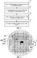
- FIG. 1 The schematic flowchart of the design method of a wafer layout in the present embodiment is shown in FIG. 1 , and the following detailed description is given with reference to FIGS. 2 and 3 .
- step 101 a yield distribution map 401 of a wafer under an initial wafer layout 51 is provided.
- the step of providing a yield distribution map 401 of a wafer under an initial wafer layout 51 includes the following operations.
- the initial wafer layout 51 is determined according to a wafer edge cleaning position 2 and a die size.
- the wafer is exposed according to the initial wafer layout 51.
- the exposed wafer is detected to obtain the yield distribution map 401 under the initial wafer layout 51.
- photoresist needs to be spin-coated on the surface of the wafer.
- redundant photoresist may be pushed to an edge 1 of the wafer under a centrifugal force, most of the photoresist is thrown away from the wafer, and part of the photoresist remains on the edge 1 of the wafer. Due to the high gas velocity of the edge 1 of the wafer, the remaining photoresist solidifies quickly, and a raised edge is formed.
- the wafer edge cleaning position 2 is a position obtained after photoresist edge repair is performed on the wafer.
- photoresist edge removal may be performed by Edge Bevel Remove (EBR) or Wafer Edge Exposure (WEE).
- the wafer edge cleaning position 2 is shown by a dashed line and is located on a side of the edge 1 of the wafer close to a center O of the wafer. No complete die can be obtained on a side of the wafer edge cleaning position 2 far away from the center O on the wafer in actual manufacturing. Therefore, when the initial wafer layout 51 is determined, the initial wafer layout 51 is determined according to the wafer edge cleaning position 2 and the die size, the wafer is exposed according to the initial wafer layout 51, and the exposed wafer is detected to obtain the yield distribution map 401 of the wafer under the initial wafer layout 51.
- the yield distribution map 401 is a position distribution map of qualified dies 41 on the wafer.
- the size of a cutting channel and the layout of dies in a single shot are also acquired, so that the initial wafer layout 51 is calculated according to the size of the cutting channel, the layout of dies in the single shot, the die size, and the wafer edge cleaning position 2.
- the size of the cutting channel is an interval distance between two adjacent dies on the wafer
- the shot is a region shot by one exposure when the wafer is exposed, and the shot may also be understood as a region on the wafer corresponding to a single exposure region of a photomask. That is, when the initial wafer layout 51 is determined, the initial wafer layout is determined jointly according to the size of the cutting channel, the layout of dies in the single shot, the die size, and the wafer edge cleaning position 2.
- step 102 a yield edge position 3 of the wafer is determined according to the yield distribution map 401.
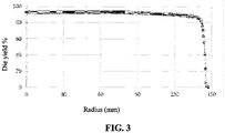
- the die yield in the radial direction of the wafer closer to the center O of the wafer is higher, and the die yield in the radial direction of the wafer closer to the edge 1 of the wafer is lower.
- the distance from the wafer edge cleaning position 2 to the center O is 147.5 mm
- the die yield at the wafer edge cleaning position 2 is 0, but the die yield actually detected is 0 at a position 147 mm from the center O. Therefore, the number of qualified dies 41 obtained after actual production is smaller than the number of complete dies in the initial wafer layout 51.
- the complete dies in the present embodiment are the complete dies calculated in the initial wafer layout 51.
- the qualified dies 41 are dies that meet the use requirements after the wafer is exposed according to the initial wafer layout 51.
- the number of qualified dies 41 is generally not the same as the number of complete qualified dies since, in actual production, the complete dies on the wafer close to the edge 1 of the wafer may be damaged without meeting the use requirements.
- a die yield at the yield edge position 3 is a preset yield value, which is smaller than a die yield at a side of the yield edge position 3 close to the center O of the wafer and is larger than or equal to a die yield at a side of the yield edge position 3 far away from the center O.
- the preset yield value is 30%, that is, if there are 100 dies at the yield edge position 3, 30 dies are qualified dies 41, and the remaining 70 dies are unqualified dies 42.
- the die yield at the side of the yield edge position 3 close to the center O of the wafer is larger than 30%, and the die yield at the side of the yield edge position 3 far away from the center O is smaller than or equal to 30%.
- the preset yield value is 0, that is, the die yield at the yield edge position 3 on the wafer is 0.
- the yield edge position 3 is shown in FIG. 2 .
- the preset yield value may also be 20%, 30%, or 50%, although it may be automatically set according to actual requirements.
- the preset yield value at the yield edge position 3 may be set to 50%.
- the dies at a low die yield position where the yield edge position 3 is far away from the center are not considered, so that qualified dies which are closely arranged are easily obtained in the new wafer layout calculated according to the die size and the yield edge position 3.
- the preset yield value of the yield edge position 3 may be set to 0, so that the total number of qualified dies obtained in the new wafer layout calculated according to the die size and the yield edge position 3 is maximum.
- the yield edge position 3 is a closed line surrounding the center O, and the closed line is a closed curve or a closed broken line.
- the closed curve and the edge 1 line of the wafer are concentric, which is convenient for determination of the yield edge position 3 on the wafer.
- the step of determining the yield edge position 3 of the wafer according to the yield distribution map 401 includes the following operations.
- a distance between the center O of the wafer and the qualified die 41 farthest away from the center O is determined as a first size.
- a closed graph is obtained by taking the center O of the wafer as an origin and the first size as a radius. The location of the closed graph is taken as the yield edge position 3.
- the yield edge position 3 is a closed curve which is concentric with the edge 1 line of the wafer, and the die yield of the yield edge position 3 is 0.
- a qualified die 41 farthest away from the center O of the wafer is determined in the yield distribution map 401.
- a distance between the center O of the wafer and the qualified die 41 farthest away from the center O is determined as a first size R1.
- a closed graph which is concentric with the edge 1 of the wafer is obtained by taking the center O of the wafer as an origin and the first size R1 as a radius.
- a location of the closed graph is taken as the yield edge position 3.
- a new wafer layout is calculated according to a die size and the yield edge position 3. Specifically, the new wafer layout is calculated according to the size of a cutting channel, the layout of dies in a single shot, the die size, and the yield edge position 3.
- step 104 the wafer is exposed according to the new wafer layout.
- a damage condition of the dies close to the wafer edge cleaning position 2 in the production process is considered when a new wafer layout is determined, the new wafer layout is determined according to the actual yield edge position 3 and the die size, and the number of obtained qualified dies 41 is approximately the same as the number of complete dies in the new wafer layout after the wafer is exposed according to the new wafer layout, thereby improving the production yield of qualified dies 41 on the wafer.
- the method further includes the following steps.
- a new yield edge position needs to be redetermined and a corrected new wafer layout is recalculated according to the new yield edge position when the yield distribution map of the wafer under the new wafer layout is changed. Therefore, the wafer layout is corrected in time according to the changed yield distribution map of the wafer, and the production yield of qualified dies 41 on the wafer is further ensured.
- the embodiments of the present application provide a design method of a wafer layout.
- the initial wafer layout 51 i.e. a wafer layout in the prior art
- the yield of dies close to the wafer edge cleaning position 2 is low or even zero due to the difference of a process control capability in the production process. Therefore, after the wafer is exposed according to the initial wafer layout 51 in the prior art, the number of obtained qualified dies 41 is often smaller than the number of complete dies in the initial wafer layout 51.
- the actual yield edge position 3 of the wafer is determined according to the yield distribution map 401 of the wafer under the initial wafer layout 51, a damage condition of the dies close to the wafer edge cleaning position 2 in the production process is considered when a new wafer layout is determined, the new wafer layout is determined according to the actual yield edge position 3 and the die size, and the number of obtained qualified dies 41 is approximately the same as the number of complete dies in the new wafer layout after the wafer is exposed according to the new wafer layout, thereby improving the production yield of qualified dies 41 on the wafer.
- a second embodiment of the present application relates to a design method of a wafer layout.
- the second embodiment is an improvement over the first embodiment.
- the main improvement is that the present embodiment provides an implementation that specifies how to determine a new wafer layout.
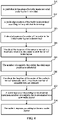
- FIG. 4 The schematic flowchart of the design method of a wafer layout in the present embodiment is shown in FIG. 4 , and the following detailed description is given with reference to FIGS. 2 and 5 .
- step 201 a yield distribution map 401 of a wafer under an initial wafer layout 51 is provided.
- step 202 a yield edge position 3 of the wafer is determined according to the yield distribution map 401.
- Steps 201 and 202 are substantially the same as steps 101 and 102 in the first embodiment. Descriptions thereof are omitted in the present embodiment to avoid repetition.
- step 203 a die 411 at a location of a center O of the wafer in the initial wafer layout 51 is determined.
- a center point of the die 411 at the location of the center O of the wafer may be made to coincide with the center O of the wafer, or, any vertex of the die 411 at the location of the center O of the wafer may be made to coincide with the center O.
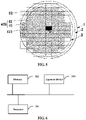
- the initial wafer layout 51 in the present embodiment is shown in FIG. 2 , and is illustrated by an example in which any vertex of the die 411 at the location of the center O of the wafer coincides with the center O.
- any point on the die 411 at the location of the center O of the wafer in the initial wafer layout 51 may coincide with the center O.
- step 204 the die 411 at the location of the center O is moved in a fixed step relative to the center O so that the initial wafer layout 51 shifts.
- the die 411 at the location of the center O is moved in a fixed step relative to the center O of the wafer, so that the initial wafer layout 51 shifts, and the die layout on the entire wafer is changed.
- the die has a transverse edge and a longitudinal edge, the transverse edge has a transverse size, the longitudinal edge has a longitudinal size, the transverse fixed step does not exceed half of the transverse size, and the longitudinal fixed step does not exceed half of the longitudinal size.
- the die 411 at the location of the center O when the die 411 at the location of the center O is moved relative to the center O, the die may be moved along the transverse direction in a fixed step which is less than half of the transverse size of the die; or, the die may be moved along the longitudinal direction in a fixed step which is less than half of the longitudinal size of the die.
- a movement direction and a movement step distance automatically.
- both the transverse fixed step and the longitudinal fixed step are smaller than 1 mm.
- step 205 the number of complete dies within the yield edge position 3 is calculated.
- step 206 the die 411 at the location of the center O of the wafer is repeatedly moved until a maximum number of complete dies are obtained.
- a shifted wafer layout is obtained after each movement of the initial wafer layout 51, and a test wafer (the test wafer has the same size as the wafer in the present application) is exposed with the shifted wafer layout so as to obtain a new yield distribution map 402 under the shifted wafer layout.
- the number of complete dies of the shifted wafer layout within the yield edge position 3 in the new yield distribution map 402 is calculated.
- Steps 204 and 205 are repeatedly executed until the calculated number of complete dies within the yield edge position 3 is maximum.
- step 207 a wafer layout corresponding to the obtained maximum number of complete dies within the yield edge position 3 is determined as a new wafer layout 52.
- step 208 the wafer is exposed according to the new wafer layout 52.
- the wafer layout corresponding to the maximum number of complete dies within the yield edge position 3 obtained in the above steps is determined as the new wafer layout 52, so that a maximum number of qualified dies 41 are obtained after the wafer is exposed by using the new wafer layout 52.
- the step of exposing the wafer according to the new wafer layout 52 includes the following operations. An initial exposure position of the die 411 at the location of the center O of the wafer in the new wafer layout 52 is determined. The wafer is exposed sequentially with a single shot according to the layout of dies in the single shot with reference to the initial exposure position.
- the embodiments of the present application provide a design method of a wafer layout.
- a specific implementation of calculating the new wafer layout 52 according to the die size and the yield edge position 3 is provided.
- the present embodiment may be implemented in conjunction with the first embodiment.
- the related technical details mentioned in the first embodiment are still valid in the present embodiment.
- the related technical details mentioned in the present embodiment may also be applied to the first embodiment.
- the technical effects that can be achieved in the first embodiment may also be achieved in the present embodiment. Descriptions thereof are omitted here to reduce repetition.
- a third embodiment of the present application relates to an exposure system of a lithography machine.
- the system includes: at least one processor 501; and a memory 502 and an exposure device 503 communicatively connected to the at least one processor 501.
- the memory 502 stores instructions executable by the at least one processor 501, and the instructions are executed by the at least one processor 501 to enable the at least one processor 501 to execute the design method of a wafer layout in any of the embodiments described above to obtain a new wafer layout 52.
- the processor 501 is configured to send the obtained new wafer layout 52 to the exposure device 503, and the exposure device 503 is configured to expose a wafer according to the new wafer layout 52.
- the memory 502 and the processor 501 are connected via a bus, which may include any number of interconnected buses and bridges.
- the bus connects various circuits of the one or more processors 501 and the memory 502 together.
- the bus may also connect various other circuits, such as peripheral devices, voltage regulators, and power management circuits, which are well known in the art and, therefore, will not be described further herein.
- a bus interface provides an interface between the bus and a transceiver.
- the transceiver may be one or more elements, such as a plurality of receivers and transmitters, which provide a unit for communicating with various other devices over a transmission medium.
- Data processed by the processor 501 is transmitted over a wireless medium via an antenna, which further receives the data and transmits the data to the processor 501.
- the processor 501 is responsible for managing the bus and general processing and may also provide various functions including timing, peripheral interfaces, voltage regulation, power management, and other control functions.
- the memory 502 may be configured to store data used by the processor 501 when performing operations.
- a fourth embodiment of the present application also provides a computer-readable storage medium storing a computer program that, when executed by a processor, implements the design method of a wafer layout in any of the embodiments described above.
- a device which may be a single-chip microcomputer, a chip, etc.
- the aforementioned storage medium includes: a U-disk, a removable hard disk, a Read-Only Memory (ROM), a Random Access Memory (RAM), a magnetic disk, an optical disk, or other media which may store program code.
Landscapes
- Engineering & Computer Science (AREA)
- Physics & Mathematics (AREA)
- Theoretical Computer Science (AREA)
- General Physics & Mathematics (AREA)
- Computer Hardware Design (AREA)
- General Engineering & Computer Science (AREA)
- Evolutionary Computation (AREA)
- Geometry (AREA)
- Architecture (AREA)
- Data Mining & Analysis (AREA)
- Databases & Information Systems (AREA)
- Mathematical Physics (AREA)
- Software Systems (AREA)
- Exposure And Positioning Against Photoresist Photosensitive Materials (AREA)
Abstract
Description
- The present application refers to
Chinese patent application No. 202010486727.0, filed on June 1, 2020 - Embodiments of the present application relate to the technical field of semiconductor, and in particular to a design method of a wafer layout and an exposure system of a lithography machine.
- Semiconductor wafers (such as wafers made of silicon, germanium, and III-V materials) are used in the manufacture of integrated circuits. Various semiconductor processes, such as lithography (e.g. patterning, etching, and deposition), epitaxial growth, doping, polishing, and other such processes, may be used on wafers to form dies. Several identical dies are usually formed on a single wafer, ranging from tens of dies per wafer to hundreds of dies per wafer or even thousands of dies per wafer, depending on the size of a device die.
- In the prior art, a wafer layout may be calculated according to a die size, an arrangement mode of dies in a single shot, and a wafer edge cleaning position, so that a maximum number of complete dies are obtained within the wafer edge cleaning position.
- However, the inventors have found that since the yield of dies in the radial distribution of wafers is not all 100% in actual production, the number of qualified dies on a single wafer during the production of a wafer layout in the prior art is often smaller than the number of calculated complete dies, so that the yield of the single wafer is low.
- Some embodiments of the present application aim at providing a design method of a wafer layout and an exposure system of a lithography machine. A large number of qualified dies are obtained during the production of a wafer layout obtained according to the design method of a wafer layout.
- In order to solve the above technical problems, the embodiments of the present application provide a design method of a wafer layout, which may include: providing a yield distribution map of a wafer under an initial wafer layout; determining a yield edge position of the wafer according to the yield distribution map; and calculating a new wafer layout according to a die size and the yield edge position.
- The embodiments of the present application also provide an exposure system of a lithography machine, which may include: at least one processor; and a memory and an exposure device communicatively connected to the at least one processor. The memory may store instructions executable by the at least one processor, and the instructions may be executed by the at least one processor to enable the at least one processor to execute the above design method of a wafer layout to obtain a new wafer layout. The processor may be configured to send the obtained new wafer layout to the exposure device, and the exposure device may be configured to expose a wafer according to the new wafer layout.
- Compared with the prior art, the embodiments of the present application provide a design method of a wafer layout. An initial wafer layout (i.e. a wafer layout in the prior art) is determined according to a die size and a wafer edge cleaning position, but the yield of dies close to the wafer edge cleaning position is low or even zero due to the difference of a process control capability in the production process. Therefore, after a wafer is exposed according to the initial wafer layout in the prior art, the number of obtained qualified dies is often smaller than the number of complete dies in the initial wafer layout. In the present embodiment, an actual yield edge position of the wafer is determined according to the yield distribution map of the wafer under the initial wafer layout, a damage condition of the dies close to the wafer edge cleaning position in the production process is considered when a new wafer layout is determined, the new wafer layout is determined according to the actual yield edge position and the die size, and the number of obtained qualified dies is approximately the same as the number of complete dies in the new wafer layout after the wafer is exposed according to the new wafer layout, thereby improving the production yield of qualified dies on the wafer.
- In addition, a die yield at the yield edge position may be a preset yield value, which may be smaller than a die yield at a side of the yield edge position close to a center of the wafer and larger than or equal to a die yield at a side of the yield edge position far away from the center.
- In addition, the preset yield value may be 0.
- In addition, the yield edge position may be a closed line surrounding the center, and the closed line may be a closed curve or a closed broken line.
- In addition, the closed curve and an edge line of the wafer may be concentric.
- In addition, the calculating a new wafer layout according to a die size and the yield edge position may include: determining a die at a location of a center of the wafer in the initial wafer layout; moving the die at the location of the center in a fixed step relative to the center to shift the initial wafer layout, where the fixed step may include a transverse fixed step and a longitudinal fixed step, the transverse fixed step may be along a transverse direction, and the longitudinal fixed step may be along a longitudinal direction; calculating the number of complete dies within the yield edge position; repeatedly moving the die at the location of the center of the wafer until a maximum number of complete dies are obtained; and determining a wafer layout corresponding to the obtained maximum number of complete dies as the new wafer layout.
- In addition, the die may have a transverse edge and a longitudinal edge, the transverse edge may have a transverse size, the longitudinal edge may have a longitudinal size, the transverse fixed step may not exceed half of the transverse size, and the longitudinal fixed step may not exceed half of the longitudinal size.
- In addition, a center point of the die at the location of the center of the wafer in the initial wafer layout may coincide with the center; or, any vertex of the die at the location of the center of the wafer in the initial wafer layout may coincide with the center.
- In addition, the providing a yield distribution map of a wafer under an initial wafer layout may include: determining the initial wafer layout according to a wafer edge cleaning position and the die size; exposing the wafer according to the initial wafer layout; and detecting the exposed wafer to obtain the yield distribution map under the initial wafer layout.
- In addition, the determining the initial wafer layout according to a wafer edge cleaning position and the die size may include: calculating the initial wafer layout according to the size of a cutting channel, the layout of dies in a single shot, the die size, and the wafer edge cleaning position.
- In addition, the determining a yield edge position of the wafer according to the yield distribution map may include: determining a distance between the center of the wafer and the qualified die farthest away from the center as a first size; and obtaining a closed graph by taking the center of the wafer as an origin and the first size as a radius, and taking a location of the closed graph as the yield edge position.
- In addition, after the calculating a new wafer layout according to a die size and the yield edge position, the method may further include: exposing the wafer according to the new wafer layout.
- In addition, the calculating a new wafer layout according to a die size and the yield edge position may include: calculating the new wafer layout according to the size of a cutting channel, the layout of dies in a single shot, the die size, and the yield edge position.
- In addition, after the calculating a new wafer layout according to a die size and the yield edge position, the method may further include the following operation.
- When the yield distribution map of the wafer is changed under the new wafer layout, a new yield edge position is redetermined, and a corrected new wafer layout is recalculated according to the new yield edge position.
- One or more embodiments are illustrated by way of example in the figures of the accompanying drawings, which are not to be construed as limiting the embodiments, and in which elements having the same reference numerals represent similar elements and in which the figures are not to scale unless otherwise indicated.
-
FIG. 1 is a schematic flowchart of a design method of a wafer layout according to a first embodiment of the present application. -
FIG. 2 is a schematic diagram of an initial wafer layout according to a first embodiment of the present application. -
FIG. 3 is a graph illustrating gradual variation of a die yield on a wafer having a radius of 150 mm with the radius according to a first embodiment of the present application. -
FIG. 4 is a schematic flowchart of a design method of a wafer layout according to a second embodiment of the present application. -
FIG. 5 is a schematic diagram of a new wafer layout according to a second embodiment of the present application. -
FIG. 6 is a schematic structure diagram of an exposure system of a lithography machine according to a third embodiment of the present application. - To more clarify the objects, technical solutions, and advantages of the embodiments of the present application, various embodiments of the present application will be described below in combination with the accompanying drawings. However, those of ordinary skill in the art will appreciate that in various embodiments of the present application, numerous technical details are set forth in order to provide readers with a better understanding of the present application. However, even without these technical details and various changes and modifications based on the following embodiments, the claimed technical solution of the present application may be implemented.
- A first embodiment of the present application relates to a design method of a wafer layout. The core of the present embodiment is as follows. A yield distribution map of a wafer under an initial wafer layout is provided. A yield edge position of the wafer is determined according to the yield distribution map. A new wafer layout is calculated according to a die size and the yield edge position. An initial wafer layout (i.e. a wafer layout in the prior art) is determined according to a die size and a wafer edge cleaning position, but the yield of dies close to the wafer edge cleaning position is low or even zero due to the difference of a process control capability in the production process. Therefore, after a wafer is exposed according to the initial wafer layout in the prior art, the number of obtained qualified dies is often smaller than the number of complete dies in the initial wafer layout. In the present embodiment, an actual yield edge position of the wafer is determined according to the yield distribution map of the wafer under the initial wafer layout, a damage condition of the dies close to the wafer edge cleaning position in the production process is considered when a new wafer layout is determined, the new wafer layout is determined according to the actual yield edge position and the die size, and the number of obtained qualified dies is approximately the same as the number of complete dies in the new wafer layout after the wafer is exposed according to the new wafer layout, thereby improving the production yield of qualified dies on the wafer.
- The implementation details of the design method of a wafer layout of the present embodiment are described in detail below, and the following description is provided only to facilitate an understanding of the implementation details provided and is not necessary to implement the present solution.
- The schematic flowchart of the design method of a wafer layout in the present embodiment is shown in
FIG. 1 , and the following detailed description is given with reference toFIGS. 2 and3 . - In
step 101, ayield distribution map 401 of a wafer under aninitial wafer layout 51 is provided. - In the present embodiment, the step of providing a
yield distribution map 401 of a wafer under aninitial wafer layout 51 includes the following operations. Theinitial wafer layout 51 is determined according to a waferedge cleaning position 2 and a die size. The wafer is exposed according to theinitial wafer layout 51. The exposed wafer is detected to obtain theyield distribution map 401 under theinitial wafer layout 51. - Specifically, before the wafer is exposed to form dies, photoresist needs to be spin-coated on the surface of the wafer. In the process of spin-coating the photoresist, redundant photoresist may be pushed to an edge 1 of the wafer under a centrifugal force, most of the photoresist is thrown away from the wafer, and part of the photoresist remains on the edge 1 of the wafer. Due to the high gas velocity of the edge 1 of the wafer, the remaining photoresist solidifies quickly, and a raised edge is formed. Therefore, after the photoresist is spin-coated, the edge 1 of the wafer is softly baked, and then the photoresist at the edge 1 of the wafer is removed chemically or optically, which is called photoresist edge repair, or photoresist edge removal. The wafer
edge cleaning position 2 is a position obtained after photoresist edge repair is performed on the wafer. Specifically, photoresist edge removal may be performed by Edge Bevel Remove (EBR) or Wafer Edge Exposure (WEE). - As shown in
FIG. 2 , the waferedge cleaning position 2 is shown by a dashed line and is located on a side of the edge 1 of the wafer close to a center O of the wafer. No complete die can be obtained on a side of the waferedge cleaning position 2 far away from the center O on the wafer in actual manufacturing. Therefore, when theinitial wafer layout 51 is determined, theinitial wafer layout 51 is determined according to the waferedge cleaning position 2 and the die size, the wafer is exposed according to theinitial wafer layout 51, and the exposed wafer is detected to obtain theyield distribution map 401 of the wafer under theinitial wafer layout 51. Theyield distribution map 401 is a position distribution map of qualified dies 41 on the wafer. - In practical applications, when the
initial wafer layout 51 is determined according to the waferedge cleaning position 2 and the die size, the size of a cutting channel and the layout of dies in a single shot are also acquired, so that theinitial wafer layout 51 is calculated according to the size of the cutting channel, the layout of dies in the single shot, the die size, and the waferedge cleaning position 2. The size of the cutting channel is an interval distance between two adjacent dies on the wafer, the shot is a region shot by one exposure when the wafer is exposed, and the shot may also be understood as a region on the wafer corresponding to a single exposure region of a photomask. That is, when theinitial wafer layout 51 is determined, the initial wafer layout is determined jointly according to the size of the cutting channel, the layout of dies in the single shot, the die size, and the waferedge cleaning position 2. - In
step 102, ayield edge position 3 of the wafer is determined according to theyield distribution map 401. - Specifically, after the
yield distribution map 401 of the wafer under theinitial wafer layout 51 is obtained, theyield distribution map 401 is detected to determine theyield edge position 3 of the wafer. The distribution of qualified dies 41 and unqualified dies 42 on the wafer can be seen from theyield distribution map 401.FIG. 3 shows a graph illustrating gradual variation of a die yield (die yield = number of qualified dies 41/total number of dies ∗ 100%) on a wafer having a radius of 150 mm with the radius is gradually changed. A specific change trend is shown in Table 1 below:Radius (mm) Die yield (%) ~ ~ 145 25 145.5 5 146 1 146.5 0.5 147 0 147.5 0 148 0 148.5 0 149 0 149.5 0 150 0 - As can be seen from
FIG. 3 and Table 1, the die yield in the radial direction of the wafer closer to the center O of the wafer is higher, and the die yield in the radial direction of the wafer closer to the edge 1 of the wafer is lower. Assuming that the distance from the waferedge cleaning position 2 to the center O is 147.5 mm, it can be seen from the above table that the die yield at the waferedge cleaning position 2 is 0, but the die yield actually detected is 0 at a position 147 mm from the center O. Therefore, the number of qualified dies 41 obtained after actual production is smaller than the number of complete dies in theinitial wafer layout 51. It should be noted that the complete dies in the present embodiment are the complete dies calculated in theinitial wafer layout 51. The qualified dies 41 are dies that meet the use requirements after the wafer is exposed according to theinitial wafer layout 51. The number of qualified dies 41 is generally not the same as the number of complete qualified dies since, in actual production, the complete dies on the wafer close to the edge 1 of the wafer may be damaged without meeting the use requirements. - In view of the above, the
yield edge position 3 is defined in the present embodiment. A die yield at theyield edge position 3 is a preset yield value, which is smaller than a die yield at a side of theyield edge position 3 close to the center O of the wafer and is larger than or equal to a die yield at a side of theyield edge position 3 far away from the center O. Assuming that the preset yield value is 30%, that is, if there are 100 dies at theyield edge position yield edge position 3 close to the center O of the wafer is larger than 30%, and the die yield at the side of theyield edge position 3 far away from the center O is smaller than or equal to 30%. - In the present embodiment, the preset yield value is 0, that is, the die yield at the
yield edge position 3 on the wafer is 0. For example, theyield edge position 3 is shown inFIG. 2 . The preset yield value may also be 20%, 30%, or 50%, although it may be automatically set according to actual requirements. The preset yield value at theyield edge position 3 may be set to 50%. At this moment, the dies at a low die yield position where theyield edge position 3 is far away from the center are not considered, so that qualified dies which are closely arranged are easily obtained in the new wafer layout calculated according to the die size and theyield edge position 3. If only the total number of qualified dies 41 is considered and the arrangement position of the qualified dies 41 is not considered, the preset yield value of theyield edge position 3 may be set to 0, so that the total number of qualified dies obtained in the new wafer layout calculated according to the die size and theyield edge position 3 is maximum. - Optionally, the
yield edge position 3 is a closed line surrounding the center O, and the closed line is a closed curve or a closed broken line. Optionally, the closed curve and the edge 1 line of the wafer are concentric, which is convenient for determination of theyield edge position 3 on the wafer. - It should be noted that the step of determining the
yield edge position 3 of the wafer according to theyield distribution map 401 includes the following operations. A distance between the center O of the wafer and thequalified die 41 farthest away from the center O is determined as a first size. A closed graph is obtained by taking the center O of the wafer as an origin and the first size as a radius. The location of the closed graph is taken as theyield edge position 3. - Specifically, description is made with an example in which the
yield edge position 3 is a closed curve which is concentric with the edge 1 line of the wafer, and the die yield of theyield edge position 3 is 0. Aqualified die 41 farthest away from the center O of the wafer is determined in theyield distribution map 401. A distance between the center O of the wafer and thequalified die 41 farthest away from the center O is determined as a first size R1. A closed graph which is concentric with the edge 1 of the wafer is obtained by taking the center O of the wafer as an origin and the first size R1 as a radius. A location of the closed graph is taken as theyield edge position 3. - In
step 103, a new wafer layout is calculated according to a die size and theyield edge position 3. Specifically, the new wafer layout is calculated according to the size of a cutting channel, the layout of dies in a single shot, the die size, and theyield edge position 3. - In
step 104, the wafer is exposed according to the new wafer layout. - Specifically with respect to
steps edge cleaning position 2 in the production process is considered when a new wafer layout is determined, the new wafer layout is determined according to the actualyield edge position 3 and the die size, and the number of obtained qualified dies 41 is approximately the same as the number of complete dies in the new wafer layout after the wafer is exposed according to the new wafer layout, thereby improving the production yield of qualified dies 41 on the wafer. - It should be noted that after a new wafer layout is calculated according to the die size and the
yield edge position 3, the method further includes the following steps. A new yield edge position needs to be redetermined and a corrected new wafer layout is recalculated according to the new yield edge position when the yield distribution map of the wafer under the new wafer layout is changed. Therefore, the wafer layout is corrected in time according to the changed yield distribution map of the wafer, and the production yield of qualified dies 41 on the wafer is further ensured. - Compared with the prior art, the embodiments of the present application provide a design method of a wafer layout. The initial wafer layout 51 (i.e. a wafer layout in the prior art) is determined according to the die size and the wafer
edge cleaning position 2, but the yield of dies close to the waferedge cleaning position 2 is low or even zero due to the difference of a process control capability in the production process. Therefore, after the wafer is exposed according to theinitial wafer layout 51 in the prior art, the number of obtained qualified dies 41 is often smaller than the number of complete dies in theinitial wafer layout 51. In the present embodiment, the actualyield edge position 3 of the wafer is determined according to theyield distribution map 401 of the wafer under theinitial wafer layout 51, a damage condition of the dies close to the waferedge cleaning position 2 in the production process is considered when a new wafer layout is determined, the new wafer layout is determined according to the actualyield edge position 3 and the die size, and the number of obtained qualified dies 41 is approximately the same as the number of complete dies in the new wafer layout after the wafer is exposed according to the new wafer layout, thereby improving the production yield of qualified dies 41 on the wafer. - A second embodiment of the present application relates to a design method of a wafer layout. The second embodiment is an improvement over the first embodiment. The main improvement is that the present embodiment provides an implementation that specifies how to determine a new wafer layout.
- The schematic flowchart of the design method of a wafer layout in the present embodiment is shown in
FIG. 4 , and the following detailed description is given with reference toFIGS. 2 and5 . - In
step 201, ayield distribution map 401 of a wafer under aninitial wafer layout 51 is provided. - In
step 202, ayield edge position 3 of the wafer is determined according to theyield distribution map 401. -
Steps steps - In
step 203, adie 411 at a location of a center O of the wafer in theinitial wafer layout 51 is determined. - Specifically, when the
initial wafer layout 51 is determined, a center point of the die 411 at the location of the center O of the wafer may be made to coincide with the center O of the wafer, or, any vertex of the die 411 at the location of the center O of the wafer may be made to coincide with the center O. Theinitial wafer layout 51 in the present embodiment is shown inFIG. 2 , and is illustrated by an example in which any vertex of the die 411 at the location of the center O of the wafer coincides with the center O. Certainly, in practical applications, any point on thedie 411 at the location of the center O of the wafer in theinitial wafer layout 51 may coincide with the center O. - In
step 204, thedie 411 at the location of the center O is moved in a fixed step relative to the center O so that theinitial wafer layout 51 shifts. - Specifically, the
die 411 at the location of the center O is moved in a fixed step relative to the center O of the wafer, so that theinitial wafer layout 51 shifts, and the die layout on the entire wafer is changed. The die has a transverse edge and a longitudinal edge, the transverse edge has a transverse size, the longitudinal edge has a longitudinal size, the transverse fixed step does not exceed half of the transverse size, and the longitudinal fixed step does not exceed half of the longitudinal size. That is, when thedie 411 at the location of the center O is moved relative to the center O, the die may be moved along the transverse direction in a fixed step which is less than half of the transverse size of the die; or, the die may be moved along the longitudinal direction in a fixed step which is less than half of the longitudinal size of the die. Certainly, in practical applications, it is also possible to set a movement direction and a movement step distance automatically. For example, both the transverse fixed step and the longitudinal fixed step are smaller than 1 mm. - In
step 205, the number of complete dies within theyield edge position 3 is calculated. - In
step 206, thedie 411 at the location of the center O of the wafer is repeatedly moved until a maximum number of complete dies are obtained. - Specifically with respect to
steps initial wafer layout 51, and a test wafer (the test wafer has the same size as the wafer in the present application) is exposed with the shifted wafer layout so as to obtain a newyield distribution map 402 under the shifted wafer layout. The number of complete dies of the shifted wafer layout within theyield edge position 3 in the newyield distribution map 402 is calculated.Steps yield edge position 3 is maximum. - In
step 207, a wafer layout corresponding to the obtained maximum number of complete dies within theyield edge position 3 is determined as anew wafer layout 52. - In
step 208, the wafer is exposed according to thenew wafer layout 52. - Specifically with respect to
steps yield edge position 3 obtained in the above steps is determined as thenew wafer layout 52, so that a maximum number of qualified dies 41 are obtained after the wafer is exposed by using thenew wafer layout 52. - In the present embodiment, the step of exposing the wafer according to the
new wafer layout 52 includes the following operations. An initial exposure position of the die 411 at the location of the center O of the wafer in thenew wafer layout 52 is determined. The wafer is exposed sequentially with a single shot according to the layout of dies in the single shot with reference to the initial exposure position. - Compared with the prior art, the embodiments of the present application provide a design method of a wafer layout. A specific implementation of calculating the
new wafer layout 52 according to the die size and theyield edge position 3 is provided. - The above division of various method steps is merely for clarity of description. During implementation, the steps may be combined into one step or some steps may be split and decomposed into a plurality of steps, which may be within the scope of protection of this patent as long as the same logical relationship is included. It is within the scope of protection of this patent to add insignificant modifications to the algorithm or the process or to introduce insignificant designs without changing the core design of the algorithm and the process.
- The present embodiment may be implemented in conjunction with the first embodiment. The related technical details mentioned in the first embodiment are still valid in the present embodiment. The related technical details mentioned in the present embodiment may also be applied to the first embodiment. The technical effects that can be achieved in the first embodiment may also be achieved in the present embodiment. Descriptions thereof are omitted here to reduce repetition.
- A third embodiment of the present application relates to an exposure system of a lithography machine. As shown in
FIG. 6 , the system includes: at least oneprocessor 501; and amemory 502 and anexposure device 503 communicatively connected to the at least oneprocessor 501. Thememory 502 stores instructions executable by the at least oneprocessor 501, and the instructions are executed by the at least oneprocessor 501 to enable the at least oneprocessor 501 to execute the design method of a wafer layout in any of the embodiments described above to obtain anew wafer layout 52. Theprocessor 501 is configured to send the obtainednew wafer layout 52 to theexposure device 503, and theexposure device 503 is configured to expose a wafer according to thenew wafer layout 52. - The
memory 502 and theprocessor 501 are connected via a bus, which may include any number of interconnected buses and bridges. The bus connects various circuits of the one ormore processors 501 and thememory 502 together. The bus may also connect various other circuits, such as peripheral devices, voltage regulators, and power management circuits, which are well known in the art and, therefore, will not be described further herein. A bus interface provides an interface between the bus and a transceiver. The transceiver may be one or more elements, such as a plurality of receivers and transmitters, which provide a unit for communicating with various other devices over a transmission medium. Data processed by theprocessor 501 is transmitted over a wireless medium via an antenna, which further receives the data and transmits the data to theprocessor 501. - The
processor 501 is responsible for managing the bus and general processing and may also provide various functions including timing, peripheral interfaces, voltage regulation, power management, and other control functions. Thememory 502 may be configured to store data used by theprocessor 501 when performing operations. - A fourth embodiment of the present application also provides a computer-readable storage medium storing a computer program that, when executed by a processor, implements the design method of a wafer layout in any of the embodiments described above.
- That is, those skilled in the art will appreciate that all or part of the steps in implementing the methods of the above embodiments may be performed by instructing related hardware via a program that is stored in a storage medium and includes a plurality of instructions for causing a device (which may be a single-chip microcomputer, a chip, etc.) or a processor to perform all or part of the steps of the methods of various embodiments of the present application. The aforementioned storage medium includes: a U-disk, a removable hard disk, a Read-Only Memory (ROM), a Random Access Memory (RAM), a magnetic disk, an optical disk, or other media which may store program code.
- It will be appreciated by those of ordinary skill in the art that the various embodiments described above are specific embodiments for implementing the present application and that various changes in form and details may be made in practice without departing from the spirit and scope of the present application.
Claims (15)
- A design method of a wafer layout, comprising:providing a yield distribution map of a wafer under an initial wafer layout;determining a yield edge position of the wafer according to the yield distribution map; andcalculating a new wafer layout according to a die size and the yield edge position.
- The design method of claim 1, wherein
a die yield at the yield edge position is a preset yield value, the preset yield value is smaller than a die yield at a side of the yield edge position close to a center of the wafer and is larger than or equal to a die yield at a side of the yield edge position far away from the center. - The design method of claim 2, wherein
the preset yield value is 0. - The design method of claim 2, wherein
the yield edge position is a closed line surrounding the center, and the closed line is a closed curve or a closed broken line. - The design method of claim 4, wherein
the closed curve and an edge line of the wafer are concentric. - The design method of claim 1, wherein the calculating a new wafer layout according to a die size and the yield edge position comprises:determining a die at a location of a center of the wafer in the initial wafer layout;moving the die at the location of the center in a fixed step relative to the center to shift the initial wafer layout, wherein the fixed step comprises a transverse fixed step and a longitudinal fixed step, the transverse fixed step is along a transverse direction, and the longitudinal fixed step is along a longitudinal direction;calculating a number of complete dies within the yield edge position;repeatedly moving the die at the location of the center of the wafer until a maximum number of complete dies are obtained; anddetermining a wafer layout corresponding to the obtained maximum number of complete dies as the new wafer layout.
- The design method of claim 6, wherein the die has a transverse edge and a longitudinal edge, the transverse edge has a transverse size, the longitudinal edge has a longitudinal size, the transverse fixed step does not exceed half of the transverse size, and the longitudinal fixed step does not exceed half of the longitudinal size.
- The design method of claim 6, whereina center point of the die at the location of the center of the wafer in the initial wafer layout coincides with the center;or,any vertex of the die at the location of the center of the wafer in the initial wafer layout coincides with the center.
- The design method of claim 1, wherein the providing a yield distribution map of a wafer under an initial wafer layout comprises:determining the initial wafer layout according to a wafer edge cleaning position and the die size;exposing the wafer according to the initial wafer layout; anddetecting the exposed wafer to obtain the yield distribution map under the initial wafer layout.
- The design method of claim 9, wherein the determining the initial wafer layout according to a wafer edge cleaning position and the die size comprises:
calculating the initial wafer layout according to a size of a cutting channel, a layout of dies in a single shot, the die size, and the wafer edge cleaning position. - The design method of claim 1, wherein the determining a yield edge position of the wafer according to the yield distribution map comprises:determining a distance between the center of the wafer and a qualified die farthest away from the center as a first size; andobtaining a closed graph by taking the center of the wafer as an origin and the first size as a radius, and taking a location of the closed graph as the yield edge position.
- The design method of claim 1, after the calculating a new wafer layout according to a die size and the yield edge position, further comprising:
exposing the wafer according to the new wafer layout. - The design method of claim 1, wherein the calculating a new wafer layout according to a die size and the yield edge position comprises:
calculating the new wafer layout according to a size of a cutting channel, a layout of dies in a single shot, the die size, and the yield edge position. - The design method of claim 1, after the calculating a new wafer layout according to a die size and the yield edge position, further comprising:
in a case where the yield distribution map of the wafer is changed under the new wafer layout, redetermining a new yield edge position, and recalculating a corrected new wafer layout according to the new yield edge position. - An exposure system of a lithography machine, comprising:at least one processor; anda memory and an exposure device communicatively connected to the at least one processor, whereinthe memory stores instructions executable by the at least one processor, the instructions being executed by the at least one processor to cause the at least one processor to execute the design method of a wafer layout of claim 1 to obtain a new wafer layout; andthe processor is configured to send the obtained new wafer layout to the exposure device, and the exposure device is configured to expose a wafer according to the new wafer layout.
Applications Claiming Priority (2)
| Application Number | Priority Date | Filing Date | Title |
|---|---|---|---|
| CN202010486727.0A CN113759665A (en) | 2020-06-01 | 2020-06-01 | Design method of wafer layout and exposure system of photoetching machine |
| PCT/CN2021/092903 WO2021244231A1 (en) | 2020-06-01 | 2021-05-10 | Design method for wafer layout and lithography machine exposure system |
Publications (2)
| Publication Number | Publication Date |
|---|---|
| EP3985715A1 true EP3985715A1 (en) | 2022-04-20 |
| EP3985715A4 EP3985715A4 (en) | 2022-11-09 |
Family
ID=78706314
Family Applications (1)
| Application Number | Title | Priority Date | Filing Date |
|---|---|---|---|
| EP21817512.3A Ceased EP3985715A4 (en) | 2020-06-01 | 2021-05-10 | SLICE ARRANGEMENT DESIGN METHOD AND LITHOGRAPHY MACHINE EXPOSURE SYSTEM |
Country Status (2)
| Country | Link |
|---|---|
| US (1) | US11657204B2 (en) |
| EP (1) | EP3985715A4 (en) |
Families Citing this family (3)
| Publication number | Priority date | Publication date | Assignee | Title |
|---|---|---|---|---|
| CN111830793B (en) * | 2020-06-22 | 2023-07-18 | 中国科学院微电子研究所 | Method and system for setting wafer exposure projection map |
| KR102841467B1 (en) * | 2020-07-29 | 2025-07-31 | 삼성전자주식회사 | Process proximity correction method and the computing device for the same |
| EP3992715B1 (en) * | 2020-09-09 | 2023-05-31 | Changxin Memory Technologies, Inc. | Wafer chip layout calculation method, medium and apparatus |
Family Cites Families (15)
| Publication number | Priority date | Publication date | Assignee | Title |
|---|---|---|---|---|
| US6604233B1 (en) * | 1999-06-28 | 2003-08-05 | Texas Instruments Incorporated | Method for optimizing the integrated circuit chip size for efficient manufacturing |
| US6522940B1 (en) | 1999-12-28 | 2003-02-18 | Koninklijke Philips Electronics N.V. | Method and system for varying die shape to increase wafer productivity |
| TW466657B (en) | 2000-06-23 | 2001-12-01 | Promos Technologies Inc | Method for calculating the yield loss |
| US6711522B2 (en) | 2001-04-25 | 2004-03-23 | Fujitsu Limited | Data analysis apparatus, data analysis method, and computer products |
| US6980917B2 (en) * | 2002-12-30 | 2005-12-27 | Lsi Logic Corporation | Optimization of die yield in a silicon wafer “sweet spot” |
| US7243325B2 (en) * | 2004-07-21 | 2007-07-10 | Bae Systems Information And Electronic Systems Integration Inc. | Method and apparatus for generating a wafer map |
| DE102006037433B4 (en) * | 2006-08-09 | 2010-08-19 | Ovd Kinegram Ag | Method for producing a multilayer body and multilayer body |
| JP2008251811A (en) * | 2007-03-30 | 2008-10-16 | Fujitsu Microelectronics Ltd | Wafer layout method and wafer layout apparatus |
| CN101311737B (en) | 2007-05-23 | 2010-11-10 | 中芯国际集成电路制造(上海)有限公司 | Wafer quality control method |
| DE102007030051B4 (en) * | 2007-06-29 | 2018-05-30 | Globalfoundries Inc. | Wafer layout optimization process and system |
| US7842521B2 (en) * | 2008-07-08 | 2010-11-30 | Palo Alto Research Center Incorporated | Edge exclusion zone patterning for solar cells and the like |
| US8148239B2 (en) * | 2009-12-23 | 2012-04-03 | Intel Corporation | Offset field grid for efficient wafer layout |
| US8965550B2 (en) | 2011-11-01 | 2015-02-24 | United Microelectronics Corp. | Experiments method for predicting wafer fabrication outcome |
| CN103187329B (en) | 2011-12-28 | 2016-06-01 | 无锡华润上华科技有限公司 | A kind of analytical method of wafer yield |
| US11163238B2 (en) * | 2019-10-04 | 2021-11-02 | Systems On Silicon Manufacturing Co. Pte. Ltd. | Optimum layout of dies on a wafer |
-
2021
- 2021-05-10 EP EP21817512.3A patent/EP3985715A4/en not_active Ceased
- 2021-08-06 US US17/395,637 patent/US11657204B2/en active Active
Also Published As
| Publication number | Publication date |
|---|---|
| US20210374316A1 (en) | 2021-12-02 |
| EP3985715A4 (en) | 2022-11-09 |
| US11657204B2 (en) | 2023-05-23 |
Similar Documents
| Publication | Publication Date | Title |
|---|---|---|
| WO2021244231A1 (en) | Design method for wafer layout and lithography machine exposure system | |
| US11657204B2 (en) | Method of wafer layout and exposure system of lithography machine | |
| US20210397101A1 (en) | Overlay compensation method, exposure system, server and readable storage medium | |
| US6248602B1 (en) | Method and apparatus for automated rework within run-to-run control semiconductor manufacturing | |
| US6245581B1 (en) | Method and apparatus for control of critical dimension using feedback etch control | |
| KR101331249B1 (en) | Method and apparatus for manufacturing data indexing | |
| US20080320434A1 (en) | Photomask management method and photomask wash limit generating method | |
| US8295965B2 (en) | Semiconductor processing dispatch control | |
| US20150279749A1 (en) | Critical size compensating method of deep groove etching process | |
| US20030039898A1 (en) | Method and system for mask pattern correction | |
| JPH11150045A (en) | Manufacturing method of semiconductor chip | |
| US20230050442A1 (en) | Systems and methods for processing semiconductor wafers using front-end processed wafer global geometry metrics | |
| CN110378073A (en) | Domain modification method and device | |
| US7915087B2 (en) | Method of arranging dies in a wafer for easy inkless partial wafer process | |
| US20210103223A1 (en) | Optimum layout of dies on a wafer | |
| US6165805A (en) | Scan tool recipe server | |
| CN105448649B (en) | A kind of arrangement method of exposing unit | |
| US10691028B2 (en) | Overlay variance stabilization methods and systems | |
| CN112446887B (en) | Wafer cutting wafer number calculating method and calculating equipment | |
| JP4524720B2 (en) | Process control device | |
| US20110093823A1 (en) | Semiconductor inter-field dose correction | |
| CN115223858B (en) | Silicon wafer processing methods | |
| KR102209725B1 (en) | Apparatus and method for predicting the performance of metrology system | |
| US20230369532A1 (en) | Stress relaxation trenches for gallium nitride microled layers on silicon substrates | |
| CN115458424B (en) | Configuration method of wafer placement rules for boat frame of vertical furnace tube equipment |
Legal Events
| Date | Code | Title | Description |
|---|---|---|---|
| STAA | Information on the status of an ep patent application or granted ep patent |
Free format text: STATUS: THE INTERNATIONAL PUBLICATION HAS BEEN MADE |
|
| PUAI | Public reference made under article 153(3) epc to a published international application that has entered the european phase |
Free format text: ORIGINAL CODE: 0009012 |
|
| STAA | Information on the status of an ep patent application or granted ep patent |
Free format text: STATUS: REQUEST FOR EXAMINATION WAS MADE |
|
| 17P | Request for examination filed |
Effective date: 20220113 |
|
| AK | Designated contracting states |
Kind code of ref document: A1 Designated state(s): AL AT BE BG CH CY CZ DE DK EE ES FI FR GB GR HR HU IE IS IT LI LT LU LV MC MK MT NL NO PL PT RO RS SE SI SK SM TR |
|
| REG | Reference to a national code |
Ref country code: DE Ref legal event code: R079 Free format text: PREVIOUS MAIN CLASS: H01L0021660000 Ipc: G03F0007200000 |
|
| A4 | Supplementary search report drawn up and despatched |
Effective date: 20221012 |
|
| RIC1 | Information provided on ipc code assigned before grant |
Ipc: H01L 21/78 20060101ALI20221006BHEP Ipc: G06F 30/392 20200101ALI20221006BHEP Ipc: G03F 7/20 20060101AFI20221006BHEP |
|
| STAA | Information on the status of an ep patent application or granted ep patent |
Free format text: STATUS: EXAMINATION IS IN PROGRESS |
|
| 17Q | First examination report despatched |
Effective date: 20230315 |
|
| DAV | Request for validation of the european patent (deleted) | ||
| DAX | Request for extension of the european patent (deleted) | ||
| REG | Reference to a national code |
Ref country code: DE Ref legal event code: R003 |
|
| STAA | Information on the status of an ep patent application or granted ep patent |
Free format text: STATUS: THE APPLICATION HAS BEEN REFUSED |
|
| 18R | Application refused |
Effective date: 20240222 |