EP3979454B1 - Device to be charged and charging method - Google Patents
Device to be charged and charging method Download PDFInfo
- Publication number
- EP3979454B1 EP3979454B1 EP19943185.9A EP19943185A EP3979454B1 EP 3979454 B1 EP3979454 B1 EP 3979454B1 EP 19943185 A EP19943185 A EP 19943185A EP 3979454 B1 EP3979454 B1 EP 3979454B1
- Authority
- EP
- European Patent Office
- Prior art keywords
- mos transistor
- terminal
- switch unit
- drive
- control
- Prior art date
- Legal status (The legal status is an assumption and is not a legal conclusion. Google has not performed a legal analysis and makes no representation as to the accuracy of the status listed.)
- Active
Links
Images


Classifications
-
- H—ELECTRICITY
- H02—GENERATION; CONVERSION OR DISTRIBUTION OF ELECTRIC POWER
- H02J—ELECTRIC POWER NETWORKS; CIRCUIT ARRANGEMENTS OR SYSTEMS FOR SUPPLYING OR DISTRIBUTING ELECTRIC POWER; SYSTEMS FOR STORING ELECTRIC ENERGY
- H02J7/00—Circuit arrangements for charging or discharging batteries or for supplying loads from batteries
- H02J7/60—Circuit arrangements for charging or discharging batteries or for supplying loads from batteries including safety or protection arrangements
- H02J7/663—Circuit arrangements for charging or discharging batteries or for supplying loads from batteries including safety or protection arrangements using battery or load disconnect circuits
-
- H—ELECTRICITY
- H02—GENERATION; CONVERSION OR DISTRIBUTION OF ELECTRIC POWER
- H02J—ELECTRIC POWER NETWORKS; CIRCUIT ARRANGEMENTS OR SYSTEMS FOR SUPPLYING OR DISTRIBUTING ELECTRIC POWER; SYSTEMS FOR STORING ELECTRIC ENERGY
- H02J7/00—Circuit arrangements for charging or discharging batteries or for supplying loads from batteries
- H02J7/90—Regulation of charging or discharging current or voltage
- H02J7/933—Regulation of charging or discharging current or voltage the cycle being controlled or terminated in response to electric parameters
-
- H—ELECTRICITY
- H02—GENERATION; CONVERSION OR DISTRIBUTION OF ELECTRIC POWER
- H02J—ELECTRIC POWER NETWORKS; CIRCUIT ARRANGEMENTS OR SYSTEMS FOR SUPPLYING OR DISTRIBUTING ELECTRIC POWER; SYSTEMS FOR STORING ELECTRIC ENERGY
- H02J1/00—Circuit arrangements for DC mains or DC distribution networks
- H02J1/08—Three-wire DC power distribution systems; Systems having more than three wires
- H02J1/082—DC supplies with two or more different DC voltage levels
-
- H—ELECTRICITY
- H02—GENERATION; CONVERSION OR DISTRIBUTION OF ELECTRIC POWER
- H02J—ELECTRIC POWER NETWORKS; CIRCUIT ARRANGEMENTS OR SYSTEMS FOR SUPPLYING OR DISTRIBUTING ELECTRIC POWER; SYSTEMS FOR STORING ELECTRIC ENERGY
- H02J7/00—Circuit arrangements for charging or discharging batteries or for supplying loads from batteries
- H02J7/02—Circuit arrangements for charging or discharging batteries or for supplying loads from batteries for charging batteries from AC mains by converters
- H02J7/04—Regulation of charging current or voltage
- H02J7/06—Regulation of charging current or voltage using discharge tubes or semiconductor devices
-
- H—ELECTRICITY
- H02—GENERATION; CONVERSION OR DISTRIBUTION OF ELECTRIC POWER
- H02J—ELECTRIC POWER NETWORKS; CIRCUIT ARRANGEMENTS OR SYSTEMS FOR SUPPLYING OR DISTRIBUTING ELECTRIC POWER; SYSTEMS FOR STORING ELECTRIC ENERGY
- H02J7/00—Circuit arrangements for charging or discharging batteries or for supplying loads from batteries
- H02J7/80—Circuit arrangements for charging or discharging batteries or for supplying loads from batteries including monitoring or indicating arrangements
-
- Y—GENERAL TAGGING OF NEW TECHNOLOGICAL DEVELOPMENTS; GENERAL TAGGING OF CROSS-SECTIONAL TECHNOLOGIES SPANNING OVER SEVERAL SECTIONS OF THE IPC; TECHNICAL SUBJECTS COVERED BY FORMER USPC CROSS-REFERENCE ART COLLECTIONS [XRACs] AND DIGESTS
- Y02—TECHNOLOGIES OR APPLICATIONS FOR MITIGATION OR ADAPTATION AGAINST CLIMATE CHANGE
- Y02E—REDUCTION OF GREENHOUSE GAS [GHG] EMISSIONS, RELATED TO ENERGY GENERATION, TRANSMISSION OR DISTRIBUTION
- Y02E60/00—Enabling technologies; Technologies with a potential or indirect contribution to GHG emissions mitigation
- Y02E60/10—Energy storage using batteries
Definitions
- the present disclosure generally relates to the technical field of charging, and in particular to a rechargeable device and a charging method.
- Rechargeable devices have got more and more consumers' favor, but have great power consumption and need to be charged frequently. It usually takes hours for these devices using a normal charging scheme with low power. To meet this challenge, a fast charging scheme, which increases the charging power of these devices, has been proposed in this industry.
- MOSFET Metal Oxide Semiconductor Field Effect Transistor
- MCU Microcontroller Unit
- the on-state impedance (i.e. RDSon) between the gate and the source becomes.
- the on-state impedance of the MOS transistor can be reduced by increasing the voltage between the gate and the source. Therefore, when the high current is used for charging, generally speaking, another MOS transistor with a smaller on-state impedance is used or the voltage between the gate and the source of the MOS transistor is increased to reduce the heat of the MOS transistor.
- the path impedance in this approach such as high design requirements for the line width and line diameter, making the design more difficult.
- US 2017/346140 A1 discloses a battery pack device with positive and negative terminals. Between said terminals, a group of cells are disposed in series with each other, and further in series with an arrangement of switches. Said arrangement of switches comprises a plurality of solid-state switches, like MOSFETs, in a variety of branches in parallel, wherein each branch comprises two switches. The solid-state switches in parallel are examples to increase the current capabilities. The two switches in each branch can be disposed in common-source or common-drain configuration. Additionally, to control the electronics, the document refers to a battery management system (BMS) or a battery management unit (BMU).
- BMS battery management system
- BMU battery management unit
- a rechargeable device includes: a charging interface; a battery unit; a first switch unit and a second switch unit coupled in parallel, coupled between the charging interface and the battery unit, a charging path defined between the battery unit and the charging interface being on and the battery unit being charged by a voltage and a current input by the charging interface, in response to the first switch unit and/or the second switch unit being turned on; a first control unit coupled to the first switch unit, configured to control the first switch unit to be turned on in response to the charging path being needed to be on, and to control both the first switch unit and the second switch unit to be turned off in response to the charging path being needed to be off; and a second control unit coupled to the second switch unit, configured to control the second switch unit to be turned on or off in response to the first control unit controlling the first switch unit to be turned on.
- a driving circuit including: a first drive MOS transistor, coupled to the first switch unit and the first control unit, respectively; and a second drive MOS transistor, coupled to the second switch unit, the first control unit, and the second control unit, respectively; wherein the first drive MOS transistor is controlled to drive the first switch unit to be turned off and the second drive MOS transistor is controlled to drive the second switch unit to be turned off, in response to a first control signal sent from the first control unit being set to be a first level; and wherein the first drive MOS transistor is controlled to drive the first switch unit to be turned on, and the second drive MOS transistor is controlled by a second control signal sent from the second control unit to drive the second switch unit to be turned on or off, in response to the first control signal sent from the first control unit being set to be a second level lower than the first level.
- a driving circuit including: a first drive MOS transistor, coupled to the first switch unit and the first control unit, respectively; and a second drive MOS transistor, coupled to the second switch unit, the first control unit,
- the control terminal of the first drive MOS transistor is coupled to the control terminal of the second drive MOS transistor via a first diode
- an anode of the first diode is coupled to the control terminal of the first drive MOS transistor
- a cathode of the first diode is coupled to the control terminal of the second drive MOS transistor
- the second control unit is coupled to the control terminal of the second drive MOS transistor via a first resistor.
- the first control unit is an MCU.
- the second control unit is an application processor.
- the first control unit further provides a clock square wave signal.
- the first switch unit includes a first MOS transistor and a second MOS transistor, wherein a first terminal of the first MOS transistor is coupled to the battery unit, a first terminal of the second MOS transistor is coupled to the charging interface via the second terminal of the first switch unit, a second terminal of the first MOS transistor is coupled to a second terminal of the second MOS transistor, and a control terminal of the first MOS transistor is coupled to a control terminal of the second MOS transistor; the first MOS transistor and the second MOS transistor are drove to be turned off such that the first switch unit is turned off, in response to the first control signal being set to be a high level; the first MOS transistor and the second MOS transistor are drove to be turned on such that the first switch unit is turned off, in response to the first control signal being set to be the second level.
- both the first terminal of the first MOS transistor and the first terminal of the second MOS transistor are sources, and both the second terminal of the first MOS transistor and the second terminal of the second MOS transistor are drains; or both the first terminal of the first MOS transistor and the first terminal of the second MOS transistor are drains, and both the second terminal of the first MOS transistor and the second terminal of the second MOS transistor are sources.
- the second switch unit includes a third MOS transistor and a fourth MOS transistor, wherein a first terminal of the third MOS transistor is coupled to the battery unit, a first terminal of the fourth MOS transistor is coupled to the charging interface, a second terminal of the third MOS transistor is coupled to a second terminal of the fourth MOS transistor, and a control terminal of the third MOS transistor is coupled to a control terminal of the fourth MOS transistor;
- the third MOS transistor and the fourth MOS transistor are drove to be turned off such that the second switch unit is turned off, in response to the first control signal via the first diode being set to be the first level;
- the third MOS transistor and the fourth MOS transistor are drove to be turned off such that the second switch unit is turned off, in response to the first control signal via the first diode being set to be the second level and the second control signal being set to be a third level;
- the third MOS transistor and the fourth MOS transistor are drove to be turned on such that the second switch unit is turned on, in response to the first
- both the first terminal of the third MOS transistor and the first terminal of the fourth MOS transistor are sources, and both the second terminal of the third MOS transistor and the second terminal of the fourth MOS transistor are drains; or both the first terminal of the third MOS transistor and the first terminal of the fourth MOS transistor are drains, and both the second terminal of the third MOS transistor and the second terminal of the fourth MOS transistor are sources.
- the first terminal of the first drive MOS transistor and the first terminal of the second drive MOS transistor are coupled to the charging interface to receive a voltage provided by the power supply device; both the second terminal of the first drive MOS transistor and the second terminal of the second drive MOS transistor are grounded.
- both the first drive MOS transistor and the second drive MOS transistor are NMOS transistors, wherein both the first terminal of the first drive MOS transistor and the first terminal of the second drive MOS transistor are drains of the NMOS transistors, and both the second terminal of the first drive MOS transistor and the second terminal of the second drive MOS transistor are sources of the NMOS transistors.
- the rechargeable device further includes a third switch unit, coupled between the charging interface and the battery unit; wherein the driving circuit is further configured to drive the third switch unit to be turned on and off and further includes a third drive MOS transistor, the third drive MOS transistor being coupled to the third switch unit; both the first control unit and the second control unit are coupled to a control terminal of the third drive MOS transistor; the third drive MOS transistor is controlled to drive the third switch unit to be turned off, in response to the first control signal sent from the first control unit being set to be a first level; the third drive MOS transistor is controlled by a third control signal sent from the second control unit to drive the third switch unit to be turned on or off, in response to the first control signal sent from the first control unit being set to be a second level lower than the first level.
- the driving circuit is further configured to drive the third switch unit to be turned on and off and further includes a third drive MOS transistor, the third drive MOS transistor being coupled to the third switch unit; both the first control unit and the second control unit are coupled to a control
- control terminal of the third drive MOS transistor is coupled to the control terminal of the first drive MOS transistor via a second diode, an anode of the second diode is coupled to the control terminal of the first drive MOS transistor, and a cathode of the second diode is coupled to the control terminal of the third drive MOS transistor; and the second control unit is coupled to the control terminal of the third drive MOS transistor via a second resistor.
- a charging method in any one rechargeable device above includes controlling, by the first control unit in the rechargeable device, both the first switch unit and the second switch unit to be turned off in response to both the first switch unit and the second switch unit being needed to be off, controlling, by the first control unit, the first switch unit to be turned on, and controlling, by the second control unit, the second switch unit to be turned on or off, in response to the first switch unit being needed to be on and the second switch unit being needed to be on or off, wherein a charging path defined between the battery unit and the charging interface is on and the battery unit is charged by a voltage and a current input by the charging interface, in response to the first switch unit and/or the second switch unit being turned on.
- the second control unit e.g. AP
- the first control unit e.g. MCU
- the second control unit e.g. AP
- plural means at least two, e.g., two, three, etc., unless otherwise expressly and specifically limited.
- "and/or" describing the association of related objects, indicates that three relationships may exist, such as A and/or B, which may indicate the presence of A alone, B alone, and both A and B.
- the symbol “/” generally indicates an "or” relationship between the associated objects that are located before and after.
- first and “second” are used for descriptive purposes only and are not to be understood as indicating or implying relative importance or implicitly specifying the number of technical features indicated. Thus, features qualified with “first” and “second” may explicitly or implicitly include one or more features.
- the "normal charging mode” and “fast charging mode” in a charging system are described.
- the adapter charges the battery in the rechargeable device by outputting a current with a relatively small value (which is usually less than 2.5A) or in a relatively small power (which is usually less than 15W).
- a relatively small value which is usually less than 2.5A
- a relatively small power which is usually less than 15W
- it usually takes several hours to fully charge a battery with a large capacity (such as a battery with a capacity of 3000 mAh).
- the adapter charges the battery in the rechargeable device by outputting a current with a relatively high current (which is usually greater than 2.5A, such as 4.5A, 5A or even higher) or in a relatively high power (which is usually greater than or equal to 15W).
- the adapter in fast charging mode has a faster charging speed and a significantly-reduced charging time required to fully charge a battery with the same capacity.
- a power supply device (such as a power adapter, a mobile Power Bank) is generally coupled to the rechargeable device through a cable, and the power supplied by the power supply device is transmitted to the rechargeable device through the cable to charge the rechargeable device.
- a MOS transistor is usually electrically coupled to a battery in a rechargeable device, and a control module is used to control a driving circuit electrically coupled to the MOS transistor to turn on and off the MOS transistor.
- the fast charging is realized to be turned on and off.
- FIG. 1 is a circuitry of a switch unit and a driving circuit of a rechargeable device in the related art according to some examples.
- the switch unit 1 may include, for example, a first MOS transistor V1 and a second MOS transistor V2.
- First poles (e.g., sources S_0 to S_2) of the first MOS transistor V1 is coupled to a battery unit via the first terminal p1
- first poles (e.g., source S_0 to S_2) of the second MOS transistor V2 is coupled to a charging interface via a second terminal p2
- a second pole (e.g., drain D) of the first MOS transistor V1 is coupled to a second pole (e.g., drain D) of the second MOS transistor V2
- a third pole (e.g., gate G) of the first MOS transistor V1 is coupled to a third pole (e.g., gate G) of the second MOS transistor V2. That is, the first MOS transistor V1 is coupled in reverse series with the second MOS transistor V2.
- a fast charging adapter is coupled, which is capable of outputting a relatively high current (which is usually greater than 2.5A, e.g. 4.5A, 5A or even higher) or a relatively high power output (which is usually greater than or equal to 15W)
- a first drive signal Fast_switch can be provided to the driving circuit 2 via a pin PIN_1 as shown in the figure, and the first drive signal Fast_switch is set to be low level.
- a MOS transistor V5 in the driving circuit 2 is cut off since the first drive signal Fast_switch is set to be low level, and a voltage VBUS provided by the power supply device is loaded between a diode D1 and a diode D2 via the diode D1.
- the second drive signal CLK_OUT which is a square wave signal provided to the driving circuit 2 via a pin PIN_2, is also loaded between the diode D1 and the diode D2.
- a resistance value of a resistor R3 is usually large (e.g. above 100K ohms), and a current flowing through resistors R1, R2 and R3 is small.
- a voltage drop caused across these resistors is also small. Therefore, a level between the diode D1 and the diode D2 is [(VBUS-Vd)+Vclk], where Vd indicates a voltage drop across the diode D1 or D2, and Vclk indicates a voltage of the square wave signal CLK_OUT. Then, after rectification of the diode D2, a level between the diode D2 and a resistor R2 becomes [(VBUS-2Vd)+Vclk] . Then, passing through the resistor R2, a gate voltage of the first MOS transistor V1 and the second MOS transistor V2 is (Vclk-2Vd).
- a voltage between the gate and the source added to the first MOS transistor V1 is [(VBUS-VBAT0)+( Vclk-2Vd)].
- the first MOS transistor V1 and the second MOS transistor V2 are enabled to be turned on, and then the fast charging is realized for the rechargeable device.
- the high current can be shunted by increasing a fast charging path.
- the fast charging path is divided into two paths, each of which is designed according to the total current divided by two.
- these two fast charging paths are controlled by one control signal, all the current will flow to the other path when one of the paths does not operates properly (e.g., due to device soldering or improper connection), and then the other path will heat up severely, or even dangerously due to overheating.
- the application processor (AP) of the rechargeable device has the possibility to die, the safety of fast charging is reduced, and a separate MCU (Microcontroller Unit) is usually used to control the fast charging.
- MCU Microcontroller Unit
- a rechargeable device which can independently control for multiple fast charging paths using independent control signals.
- FIG. 2 is a block diagram of a rechargeable device according to some exemplary embodiments.
- the rechargeable device 10 as shown in FIG. 2 may be, for example, a terminal or a communication terminal that includes, but is not limited to, a device provided to be coupled via a wired line such as a public switched telephone network (PSTN), a digital subscriber line (DSL), a digital cable, a direct cable connection, and/or another data connection/network, and/or via, for example, cellular networks, a wireless local area network (WLAN), a digital video network such as a digital video broadcasting handheld (DVB-H) network, a satellite network, an amplitude modulation-frequency modulation (AM-FM) broadcast transmitter, and/or a wireless interface of another communication terminal to receive/send communication signals.
- PSTN public switched telephone network
- DSL digital subscriber line
- WLAN wireless local area network
- DVD-H digital video broadcasting handheld
- AM-FM amplitude modulation-frequency modulation
- a communication terminal set to communicate via a wireless interface may be referred to as a "wireless communication terminal", a “wireless terminal”, and/or a “mobile terminal”.
- mobile terminals include, but are not limited to, satellite or cellular telephones, personal communication system (PCS) terminals that can combine cellular radio telephony with data processing, fax, and data communication capabilities, Personal Digital Assistant (PDA) containing radio telephones, pagers, Internet/Intranet access, Web browsers, notepads, calendars, and/or global positioning systems (GPS) receivers, and a conventional lap top and/or handheld receiver or other electronic device containing a radio telephone transceiver.
- PCS personal communication system
- GPS global positioning systems
- the terminal may also include, but is not limited to, a rechargeable electronic device with charging capabilities such as an e-book reader, a smart wearable device, a mobile power source (e.g., rechargeable battery, travel charger), an electronic cigarette, a wireless mouse, a wireless keyboard, a wireless headset, a Bluetooth speaker, etc.
- a rechargeable electronic device with charging capabilities such as an e-book reader, a smart wearable device, a mobile power source (e.g., rechargeable battery, travel charger), an electronic cigarette, a wireless mouse, a wireless keyboard, a wireless headset, a Bluetooth speaker, etc.
- the rechargeable device 10 includes a charging interface 11, a battery unit 12, a first switch unit 13a, a second switch unit 13b, a first control unit 15a, and a second control unit 15b.
- the charging interface 11 can be, for example, a USB 2.0 interface, a micro USB interface, or a USB TYPE-C interface. In some embodiments, the charging interface 11 may also be a lightning interface, or any other type of parallel or serial port capable of being used for charging.
- the battery unit 12 may be a lithium battery containing a single lithium battery cell, or a lithium battery containing multiple lithium battery cells. Alternatively, the battery unit 12 may also contain multiple battery cells, each of which contains one or more lithium battery cells.
- the first switch unit 13a and the second switch unit 13b are coupled in parallel and coupled between the charging interface 11 and the battery unit 12.
- the charging path is one in a first charging mode
- the battery unit 12 is charged by a voltage and a current input through the charging interface 11.
- the charging path is off, and other charging paths, for example, one in a second charging mode, can be turned on in the rechargeable device 10 to charge the rechargeable device 10 in the second charging mode. That is, the first switch unit 13a and the second switch unit 13b are used to control turning on and off of the charging path in the first charging mode. Furthermore, it should be understood by those skilled in the art that the two charging paths cannot be turned on simultaneously, i.e. the rechargeable device 10 can only operate in one charging mode.
- the first charging mode can be, for example, the fast charging mode described above
- the second charging mode can be, for example, the normal charging mode described above.
- a charging power in the first charging mode is greater than that in the second charging mode.
- the first control unit 15a is coupled to the first switch unit 13a and is used for controlling the first switch unit 13a to be turned on when the charging path between the charging interface and the battery unit is needed to be on.
- the second control unit 15b is coupled to the second switch unit 13b and is used for controlling the second switch unit 13b to be turned on or off when the first control unit 15a controls the first switch unit 13a to be turned on.
- the first control unit 15a is also used to control both the first switch unit 13a and the second switch unit 13b to be turned off when the charging path between the charging interface 11 and the battery unit 12 (i.e., the charging path in the first charging mode described above) is needed to be off.
- the first control unit 15a may be, for example, a microcontroller MCU, and the second control unit 15c may be, for example, an application processor.
- the MCU has less I/O interface resources, it is not possible to provide multiple independent control signals to control multiple fast charging paths (e.g., first switch unit 13a and second switch unit 13b) separately and independently at the same time.
- the AP has a lot of I/O interface resources, it is worried that the AP will not be able to shut down the fast charging paths in time after the AP dies if the AP is used to control one or more of the multiple fast charging paths, and this will cause danger.
- the rechargeable device 10 provided in the present disclosure can ensure the safety of fast charging in the case where multiple independent control signals are used.
- the second control unit 15b is allowed to control the second switch unit 13b to be turned on or off. If a problem such as a dead AP occurs, the first control unit 15a can immediately control the first switch unit 13a and the second switch unit 13b to be turned off, and then the fast charging mode is over.
- FIG. 3 is a block diagram of another rechargeable device according to some exemplary embodiments.
- the rechargeable device 20 includes a charging interface 11, a battery unit 12, a first switch unit 13a, a second switch unit 13b, a first control unit 15a, and a second control unit 15b.
- the rechargeable device 20 is coupled to a power supply device 40 via the charging interface 11 to charge a battery unit 12.
- the charging interface 11 can be, for example, a USB 2.0 interface, a micro USB interface, or a USB TYPE-C interface. In some embodiments, the charging interface 11 may also be a lightning interface, or any other type of parallel or serial port capable of being used for charging.
- the battery unit 12 may be a lithium battery containing a single lithium battery cell, or a lithium battery containing multiple lithium battery cells. Alternatively, the battery unit 12 may also contain multiple battery cells, each of which contains one or more lithium battery cells.
- a modified battery structure can be used in which multiple cells are used to be coupled in series with each other, and the multiple cells are charged directly. That is, a voltage output from the adapter is loaded directly to both ends of the battery unit containing the multiple cells.
- the charging current required for the multiple cells is about 1/N (N is the number of cells coupled in series) of the charging current required for the single cell if the same charging speed is to be achieved.
- N is the number of cells coupled in series
- the multiple cells coupled in series can significantly reduce a size of the charging current, which thus further reduces the heat generation of the rechargeable device in the charging process.
- the first switch unit 13a includes a first terminal pla, a second terminal p2a, and a third terminal p3a.
- the first terminal p1a is coupled to the battery unit 12, the second terminal p2a is coupled to the charging interface 11, and the third terminal p3a is coupled to the driving circuit 14.
- the second switch unit 13b includes a first terminal plb, a second terminal p2b, and a third terminal p3b.
- the first terminal p1b is coupled to the battery unit 12, the second terminal p2b is coupled to the charging interface 11, and the third terminal p3b is coupled to the driving circuit 14.
- the driving circuit 14 is used to drive the first switch unit 13a and the second switch unit 13b to be turned on and off, respectively, and thus control starting and ending of the fast charging.
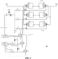
- FIG. 4 is a circuitry schematic diagram of a rechargeable device according to some exemplary embodiments.
- each MOS transistor in FIG. 4 is an example of an NMOS transistor, which is also used as an example in the following description and explanation of the principle. However, it will be understood by those skilled in the art how to apply the method provided by the embodiments of the present disclosure when each MOS transistor is replaced with a PMOS transistor based on the same inventive concept.
- the driving circuit 14 includes a first drive MOS transistor V5a and a second drive MOS transistor V5b.
- a first terminal (e.g., drain D) of the first drive MOS transistor V5a is coupled to the third terminal p3a of the first switch unit 13a.
- a first terminal (e.g., drain D) of the second drive MOS transistor V5b is coupled to the third terminal p3b of the second switch unit 13b.
- a control terminal (i.e. gate G) of the first drive MOS transistor V5a is coupled to a control terminal (i.e.
- a first interface I1a of the first control unit 15a is coupled to a first pin Pin1 of the driving circuit 14 so that the first control unit 15a is coupled to the control terminal of the first drive MOS transistor V5a.
- a first interface I1b of the second control unit 15b is coupled to a second pin Pin2 of the driving circuit 14 via a first resistor R5a, such that the second control unit 15b is coupled to the control terminal of the second driver MOS transistor V5b.
- two independent control signals FAST_SWITCH_1 and FAST_SWITCH_2 are designed to control the first switch unit 13a and the second switch unit 13b, respectively, in the rechargeable device 20 of the present disclosure.
- the MCU has less I/O interface resources, it is not possible to provide multiple independent control signals to control multiple fast charging paths (e.g., first switch unit 13a and second switch unit 13b) separately and independently at the same time.
- the AP has a lot of I/O interface resources, it is worried that the AP will not be able to shut down the fast charging paths in time after the AP dies if the AP is used to control one or more of the multiple fast charging paths, and this will cause danger.
- the rechargeable device 20 provided in the present disclosure can ensure the safety of fast charging in the case where multiple independent control signals are used.
- the control terminals of the first drive MOS transistor V5a and the second drive MOS transistor V5b are set to be a high level, so that both the first drive MOS transistor V5a and the second drive MOS transistor V5b are turned on.
- the first switch unit 13a and the second switch unit 13b are turned off, i.e. both fast charging paths are closed.
- the second control unit 15b inputs the control signal FAST_SWITCH_2 with a low level through the second pin Pin2 of the driving circuit 14, the control terminal of the second drive MOS transistor V5b is still in a high level due to the first resistor R5a, and the second drive MOS transistor V5b is still on.
- the second switch unit 13b still cannot be turned on, i.e., the fast charging path cannot be on.
- the control terminal of the first drive MOS transistor V5a is set to be a low level, and then the first drive MOS transistor V5a is turned off.
- the first switch unit 13a is turned on, i.e. the fast charging path is on.
- the control terminal of the second drive MOS transistor V5b is not set to be a low level as FAST_SWITCH_1 is low.
- the second control unit 15b can turn off the second drive MOS transistor V5b, and then turn on the second switch unit 13b.
- the second control unit 15b can also turn on the second drive MOS transistor V5b, and then turn off the second switch unit 13b.
- the second control unit 15b can control starting or ending of the other fast charging path only when the first control unit 15a agrees to start the fast charging path, i.e., when the first control unit 15a inputs the control signal FAST_SWITCH_1 with a low level. And if the first control unit 15b does not agree to the fast charging path, the second control unit 15b will fail to control the other fast charging path. Thus, this ensures that even after the second control unit 15b dies, both charging paths can be turned off simultaneously by the first control unit 15a, avoiding the danger that the fast charging path cannot be turned off as the second control unit 15b dies.
- the first control unit 15a may also provide a clock square wave signal CLK_OUT for the driving circuit 14 through its second interface I2a and the third pin Pin3 of the driving circuit 14.
- the first switch unit 13a may include a first MOS transistor V1a and a second MOS transistor V2a.
- First terminals (e.g., sources S_0 to S_2 as shown in FIG. 4 ) of the first MOS transistor V1a are coupled to the battery unit 12 (i.e. VBAT in FIG. 4 ) through the first terminal p1a of the first switch unit 13a, first terminals (e.g. source S_0 to S_2 as shown in FIG. 4 ) of the second MOS transistor V2a are coupled to the charging interface 11 (i.e. VBUS in FIG.
- a second terminal of the first MOS transistor V1a (e.g., drain D as shown in FIG. 4 ) is coupled to a second terminal of the second MOS transistor V2a (e.g., drain D as shown in FIG. 4 ), and a control terminal (i.e. gate G) of the first MOS transistor V1a is coupled to a control terminal (i.e. gate G) of the second MOS transistor V2a.
- both the first terminal of the first MOS transistor V1a and the first terminal of the second MOS transistor V2a may also be drains, and both the second terminal of the first MOS transistor V1a and the second terminal of the second MOS transistor V2a may be sources. That is, it is sufficient that the first MOS transistor V1a is coupled in reverse series with the second MOS transistor V2a, and thus power is supplied to the rechargeable device 20 through the power supply device 40 when the battery unit 12 is charged.
- the second switch unit 13b may include a third MOS transistor V1b and a fourth MOS transistor V2b.
- First terminals (e.g., sources S_0 to S_2 as shown in FIG. 4 ) of the third MOS transistor V1b are coupled to the battery unit 12 through the first terminal p1b of the second switch unit 13b
- first terminals (e.g., source S_0 to S _2 as shown in FIG. 4 ) of the fourth MOS transistor V2b are coupled to the charging interface 11 through the second terminal p2b of the second switch unit 13b
- a second terminal (e.g., drain D as shown in FIG. 4 ) of the third MOS transistor V1b is coupled to a second terminal (e.g., drain D as shown in FIG. 4 ) of the fourth MOS transistor V2b
- a control terminal (i.e. gate G) of the third MOS transistor V1b is coupled to a control terminal (i.e. gate G) of the fourth MOS transistor V2
- both the first terminal of the third MOS transistor V1b and the first terminal of the fourth MOS transistor V2b may also be drains, and both the second terminal of the third MOS transistor V1b and the second terminal of the fourth MOS transistor V2b may be sources. That is, it is sufficient that the third MOS transistor V1b is coupled in reverse series with the fourth MOS transistor V2b, and thus power is supplied to the rechargeable device 20 through the power supply device 40 when the battery unit 12 is charged.
- the first terminal (e.g., drain D as shown in FIG. 4 ) of the first drive MOS transistor V5a is coupled to the charging interface 11 via a diode D1, a diode D2 and a resistor R2a to receive the voltage VBUS provided by the power supply device 40.
- the first terminal (e.g., drain D as shown in FIG. 4 ) of the second drive MOS transistor V5b is coupled to the charging interface 11 via the diode D1, the diode D2 and a resistor R2b to receive the voltage VBUS provided by the power supply device 40.
- Both the second terminal (e.g., source S as shown in FIG. 4 ) of the first drive MOS transistor V5a and the second terminal (e.g., source S as shown in FIG. 4 ) of the second drive MOS transistor V5b are grounded.
- both the first drive MOS transistor V5a and the second drive MOS transistor V5b may be NMOS (N-type Metal Oxide Semiconductor) transistors, where both the first terminal of the first drive MOS transistor V5a and the first terminal of the second drive MOS transistor V5b are drains D of the NMOS transistors, and both the second terminal of the first drive MOS transistor V5a and the second terminal of the second drive MOS transistor V5b are sources S of the NMOS transistors.
- NMOS N-type Metal Oxide Semiconductor
- the AP can be used to control multiple fast charging paths because of its more abundant input/output interface resources.
- FIG. 5 is a circuitry schematic diagram of another rechargeable device according to some exemplary embodiments.
- the rechargeable device 20' shown in FIG. 5 also includes a third switch unit 13c.
- the third switch unit 13c includes a first terminal plc, a second terminal p2c, and a third terminal p3c.
- the first terminal p1c of the third switch unit 13c is coupled to the battery unit 12, and the second terminal p2c of the third switch unit 13c is coupled to the charging interface 11.
- the driving circuit 14 is also used to drive the third switch unit 13c to be turned on and off.
- the driving circuit 14 also includes a third drive MOS transistor V5c.
- a first terminal e.g., drain D as shown in FIG.
- the third drive MOS transistor V5c is coupled to a third terminal p3c of the third switch unit 13c, a control terminal (i.e. gate G) of the third drive MOS transistor V5c is coupled to the control terminal of the first drive MOS transistor V5a via a second diode D4b.
- An anode of the second diode D4b is coupled to the control terminal (i.e. gate G) of the first drive MOS transistor V5a, and a cathode of the second diode D4b is coupled to the control terminal (i.e. gate G) of the third drive MOS transistor V5c.
- the second interface I2b of the second control unit 15b is coupled to a fourth pin Pin4 of the driving circuit 14 through a second resistor R5b, and thus, the second control unit 15b is coupled to the control terminal (i.e. gate G) of the third drive MOS transistor V5c and inputs a control signal FAST_SWITCH_3 to the third drive MOS transistor V5c.
- the third drive MOS transistor V5c is also a NMOS as an example, but the present disclosure is not limited to this.
- the third switch unit 13c may include a fifth MOS transistor V1c and a sixth MOS transistor V2c.
- First terminals (e.g., sources S_0 to S_2 as shown in FIG. 5 ) of the fifth MOS transistor V1c are coupled to the battery unit 12 through the first terminal p1c of the third switch unit 13c, first terminals (e.g., sources S_0 to S_2 as shown in FIG. 5 ) of the fourth MOS transistor V2b are coupled to the battery unit 12 (i.e. VBAT in FIG.
- first terminals (e.g., source S_0 to S _2) of the sixth MOS transistor V2c are coupled to the charging interface 11 (i.e. VBUS in FIG. 5 ) through the second terminal p2c of the third switch unit 13c, a second terminal (e.g., drain D as shown in FIG. 5 ) of the fifth MOS transistor V1c is coupled to a second terminal (e.g., drain D as shown in FIG.5 ) of the sixth MOS transistor V2c, and a control terminal (i.e. gate G) of the fifth MOS transistor V1c is coupled to a control terminal (i.e. gate G) of the sixth MOS transistor V2c.
- both the first terminal of the fifth MOS transistor V1c and the first terminal of the sixth MOS transistor V2c may also be drains, and both the second terminal of the fifth MOS transistor V1c and the second terminal of the sixth MOS transistor V2c may be sources. That is, it is sufficient that the fifth MOS transistor V1c is coupled in reverse series with the sixth MOS transistor V2c, and thus power is supplied to the rechargeable device 20' through the power supply device 40 when the battery unit 12 is charged.
- the first terminal (e.g., drain D as shown in FIG. 5 ) of the third drive MOS transistor V5c is coupled to the charging interface 11 via a diode D1, a diode D2, and a resistor R2c to receive the voltage VBUS provided by the power supply device 40.
- the second terminal (e.g., source S as shown in FIG. 5 ) of the third drive MOS transistor V5c is grounded.
- the third drive MOS transistor V5c may be an NMOS transistor, as shown in FIG. 5 , where the first terminal of the third drive MOS transistor V5c is the drain D of the NMOS transistor and the second terminal of the third drive MOS transistor V5c is the source S of the NMOS transistor.
- the control terminal of the third drive MOS transistor V5c is coupled to the second control unit 15b, only when the first control unit 15a inputs a control signal FAST SWITCH_1 with a low level to the control terminal of the first drive MOS transistor V5a through the first interface I1a, the second control unit 15b inputs a control signal FAST_SWITCH_3 to the third drive MOS transistor V5c via its second interface I2b to effectively control the third drive MOS transistor V5c.
- the second control unit 15b can control the third drive MOS transistor V5c to be turned on or off correspondingly, and thus control a corresponding fast charging path to be turned on and off.
- the second control unit 15b is in a situation such as dead, all fast charging paths can be quickly shut down by the first control unit 15a to avoid danger.
- FIG. 1 For the sake of simplifying the accompanying drawings, other components in FIG. 1 that play a protective function are omitted in both FIG. 4 and FIG. 5 .
- the second control unit e.g. AP
- the first control unit e.g. MCU
- the second control unit e.g. AP
- the present disclosure describes how to form and use particular examples, but the principles of the present disclosure are not limited to any details of these examples. Rather, these principles can be applied to many other embodiments based on the teachings disclosed in the present disclosure.
- FIG. 6 is a flowchart of a charging method according to some exemplary embodiments.
- the charging method 30 may be applied, for example, in the device 20, 10 or 10' to be charged as described above, and include actions/operations in the following.
- the method controls the first switch unit and the second switch unit to be turned off by the first control unit in the rechargeable device, in response to both the first switch unit and the second switch unit in the rechargeable device being needed to be turned off.
- controlling the first switch unit and the second switch unit to be turned off by the first control unit in the rechargeable device includes: controlling a first drive MOS transistor and a second drive MOS transistor in the rechargeable device to drive the first switch unit and the second switch unit to be turned off, respectively, in response to a first control signal sent to the first drive MOS transistor by the first control unit being set to be a high level.
- the method controls the first switch unit to be turned on by the first control unit, and controls the second switch unit to be turned on or off by a second control unit in the rechargeable device, in response to the first switch unit being needed to be turned on and the second switch unit being needed to be turned on or off.
- the charging path between a charging interface in the rechargeable device and a battery unit in the rechargeable device is on, and the battery unit is charged by a voltage and a current input through the charging interface.
- the controlling, by the first control unit, the first switch unit to be turned on includes controlling, by the first control unit, a first drive MOS transistor to drive the first switch unit to be turned on, in response to a first control signal sent to the first drive MOS transistor from the first control unit being set to be a low level.
- controlling, by the second control unit in the rechargeable device, the second switch unit to be turned on or off includes controlling, by the second control unit, a second drive MOS transistor in the rechargeable device to drive the second switch unit to be turned on or off via a second control signal sent to the second drive MOS transistor from the second control unit, in response to the first switch unit being turned on.
- the method 30 further includes: controlling the first switch unit and the third switch unit to be turned off by the first control unit in the rechargeable device, in response to both the first switch unit and the third switch unit in the rechargeable device being needed to be turned off; and controlling the first switch unit to be turned on by the first control unit, and controlling the third switch unit to be turned on or off by a second control unit in the rechargeable device, in response to the first switch unit being needed to be turned on and the third switch unit being needed to be turned on or off.
- controlling the first switch unit and the third switch unit to be turned off by the first control unit in the rechargeable device includes: controlling the first drive MOS transistor and a third drive MOS transistor in the rechargeable device to drive the first switch unit and the third switch unit to be turned off, respectively, in response to a first control signal sent to the first drive MOS transistor by the first control unit being set to be a high level.
- the controlling, by the first control unit, the first switch unit to be turned on includes controlling, by the first control unit, a first drive MOS transistor to drive the first switch unit to be turned on, in response to a first control signal sent to the first drive MOS transistor from the first control unit being set to be a low level.
- controlling, by the second control unit in the rechargeable device, the third switch unit to be turned on or off includes controlling, by the second control unit, a third drive MOS transistor in the rechargeable device to drive the third switch unit to be turned on or off via a second control signal sent to the third drive MOS transistor from the second control unit, in response to the first switch unit being turned on.
Landscapes
- Engineering & Computer Science (AREA)
- Power Engineering (AREA)
- Charge And Discharge Circuits For Batteries Or The Like (AREA)
Description
- The present disclosure generally relates to the technical field of charging, and in particular to a rechargeable device and a charging method.
- Rechargeable devices have got more and more consumers' favor, but have great power consumption and need to be charged frequently. It usually takes hours for these devices using a normal charging scheme with low power. To meet this challenge, a fast charging scheme, which increases the charging power of these devices, has been proposed in this industry.
- In order to increase the charging power of these devices and thus achieve fast charging, one option is to use high current to charge these devices. The higher the charging current is, and the faster the charging speed of these devices will be. In a fast charging scheme, a MOSFET (Metal Oxide Semiconductor Field Effect Transistor, abbreviated as MOS transistor) is usually electrically coupled to batteries in these devices, and a control module such as an MCU (Microcontroller Unit) is used to control a driving circuit electrically coupled to the MOS transistor to turn on and off the MOS transistor. Thus, the fast charging is realized to be turn on and off.
- In this connection, according to the characteristics of the MOS transistor, when the voltage between the gate and the source is located in a certain range, the smaller the on-state impedance (i.e. RDSon) between the gate and the source becomes. Thus, the on-state impedance of the MOS transistor can be reduced by increasing the voltage between the gate and the source. Therefore, when the high current is used for charging, generally speaking, another MOS transistor with a smaller on-state impedance is used or the voltage between the gate and the source of the MOS transistor is increased to reduce the heat of the MOS transistor. However, there usually requires high design requirements for the path impedance in this approach, such as high design requirements for the line width and line diameter, making the design more difficult.
-
US 2017/346140 A1 discloses a battery pack device with positive and negative terminals. Between said terminals, a group of cells are disposed in series with each other, and further in series with an arrangement of switches. Said arrangement of switches comprises a plurality of solid-state switches, like MOSFETs, in a variety of branches in parallel, wherein each branch comprises two switches. The solid-state switches in parallel are examples to increase the current capabilities. The two switches in each branch can be disposed in common-source or common-drain configuration. Additionally, to control the electronics, the document refers to a battery management system (BMS) or a battery management unit (BMU). - The above information disclosed in the described background technology is intended only to enhance the understanding of the background of this disclosure, and therefore it may include information that does not constitute prior art known to those ordinary skill in the art.
- In the view of the above, a rechargeable device and a charging method are provided.
- Other features and advantages of the present disclosure will become apparent through the following detailed description, or will be learned in part through the practice of the present disclosure.
- According to one aspect of the present disclosure, a rechargeable device is provided. The rechargeable device includes: a charging interface; a battery unit; a first switch unit and a second switch unit coupled in parallel, coupled between the charging interface and the battery unit, a charging path defined between the battery unit and the charging interface being on and the battery unit being charged by a voltage and a current input by the charging interface, in response to the first switch unit and/or the second switch unit being turned on; a first control unit coupled to the first switch unit, configured to control the first switch unit to be turned on in response to the charging path being needed to be on, and to control both the first switch unit and the second switch unit to be turned off in response to the charging path being needed to be off; and a second control unit coupled to the second switch unit, configured to control the second switch unit to be turned on or off in response to the first control unit controlling the first switch unit to be turned on.
- According to some embodiments of the present disclosure, further including: a driving circuit, including: a first drive MOS transistor, coupled to the first switch unit and the first control unit, respectively; and a second drive MOS transistor, coupled to the second switch unit, the first control unit, and the second control unit, respectively; wherein the first drive MOS transistor is controlled to drive the first switch unit to be turned off and the second drive MOS transistor is controlled to drive the second switch unit to be turned off, in response to a first control signal sent from the first control unit being set to be a first level; and wherein the first drive MOS transistor is controlled to drive the first switch unit to be turned on, and the second drive MOS transistor is controlled by a second control signal sent from the second control unit to drive the second switch unit to be turned on or off, in response to the first control signal sent from the first control unit being set to be a second level lower than the first level.
- According to some embodiments of the present disclosure, the control terminal of the first drive MOS transistor is coupled to the control terminal of the second drive MOS transistor via a first diode, an anode of the first diode is coupled to the control terminal of the first drive MOS transistor, and a cathode of the first diode is coupled to the control terminal of the second drive MOS transistor; and the second control unit is coupled to the control terminal of the second drive MOS transistor via a first resistor.
- According to some embodiments of the present disclosure, the first control unit is an MCU.
- According to some embodiments of the present disclosure, the second control unit is an application processor.
- According to some embodiments of the present disclosure, the first control unit further provides a clock square wave signal.
- According to some embodiments of the present disclosure, the first switch unit includes a first MOS transistor and a second MOS transistor, wherein a first terminal of the first MOS transistor is coupled to the battery unit, a first terminal of the second MOS transistor is coupled to the charging interface via the second terminal of the first switch unit, a second terminal of the first MOS transistor is coupled to a second terminal of the second MOS transistor, and a control terminal of the first MOS transistor is coupled to a control terminal of the second MOS transistor; the first MOS transistor and the second MOS transistor are drove to be turned off such that the first switch unit is turned off, in response to the first control signal being set to be a high level; the first MOS transistor and the second MOS transistor are drove to be turned on such that the first switch unit is turned off, in response to the first control signal being set to be the second level.
- According to some embodiments of the present disclosure, both the first terminal of the first MOS transistor and the first terminal of the second MOS transistor are sources, and both the second terminal of the first MOS transistor and the second terminal of the second MOS transistor are drains; or both the first terminal of the first MOS transistor and the first terminal of the second MOS transistor are drains, and both the second terminal of the first MOS transistor and the second terminal of the second MOS transistor are sources.
- According to some embodiments of the present disclosure, the second switch unit includes a third MOS transistor and a fourth MOS transistor, wherein a first terminal of the third MOS transistor is coupled to the battery unit, a first terminal of the fourth MOS transistor is coupled to the charging interface, a second terminal of the third MOS transistor is coupled to a second terminal of the fourth MOS transistor, and a control terminal of the third MOS transistor is coupled to a control terminal of the fourth MOS transistor; the third MOS transistor and the fourth MOS transistor are drove to be turned off such that the second switch unit is turned off, in response to the first control signal via the first diode being set to be the first level; the third MOS transistor and the fourth MOS transistor are drove to be turned off such that the second switch unit is turned off, in response to the first control signal via the first diode being set to be the second level and the second control signal being set to be a third level; the third MOS transistor and the fourth MOS transistor are drove to be turned on such that the second switch unit is turned on, in response to the first control signal via the first diode being set to be a low level and the second control signal being set to be a fourth level lower than the third level.
- According to some embodiments of the present disclosure, both the first terminal of the third MOS transistor and the first terminal of the fourth MOS transistor are sources, and both the second terminal of the third MOS transistor and the second terminal of the fourth MOS transistor are drains; or both the first terminal of the third MOS transistor and the first terminal of the fourth MOS transistor are drains, and both the second terminal of the third MOS transistor and the second terminal of the fourth MOS transistor are sources.
- According to some embodiments of the present disclosure, the first terminal of the first drive MOS transistor and the first terminal of the second drive MOS transistor are coupled to the charging interface to receive a voltage provided by the power supply device; both the second terminal of the first drive MOS transistor and the second terminal of the second drive MOS transistor are grounded.
- According to some embodiments of the present disclosure, both the first drive MOS transistor and the second drive MOS transistor are NMOS transistors, wherein both the first terminal of the first drive MOS transistor and the first terminal of the second drive MOS transistor are drains of the NMOS transistors, and both the second terminal of the first drive MOS transistor and the second terminal of the second drive MOS transistor are sources of the NMOS transistors.
- According to some embodiments of the present disclosure, the rechargeable device further includes a third switch unit, coupled between the charging interface and the battery unit; wherein the driving circuit is further configured to drive the third switch unit to be turned on and off and further includes a third drive MOS transistor, the third drive MOS transistor being coupled to the third switch unit; both the first control unit and the second control unit are coupled to a control terminal of the third drive MOS transistor; the third drive MOS transistor is controlled to drive the third switch unit to be turned off, in response to the first control signal sent from the first control unit being set to be a first level; the third drive MOS transistor is controlled by a third control signal sent from the second control unit to drive the third switch unit to be turned on or off, in response to the first control signal sent from the first control unit being set to be a second level lower than the first level.
- According to some embodiments of the present disclosure, the control terminal of the third drive MOS transistor is coupled to the control terminal of the first drive MOS transistor via a second diode, an anode of the second diode is coupled to the control terminal of the first drive MOS transistor, and a cathode of the second diode is coupled to the control terminal of the third drive MOS transistor; and the second control unit is coupled to the control terminal of the third drive MOS transistor via a second resistor.
- According to another aspect of the present disclosure, a charging method in any one rechargeable device above is provided, which includes controlling, by the first control unit in the rechargeable device, both the first switch unit and the second switch unit to be turned off in response to both the first switch unit and the second switch unit being needed to be off, controlling, by the first control unit, the first switch unit to be turned on, and controlling, by the second control unit, the second switch unit to be turned on or off, in response to the first switch unit being needed to be on and the second switch unit being needed to be on or off, wherein a charging path defined between the battery unit and the charging interface is on and the battery unit is charged by a voltage and a current input by the charging interface, in response to the first switch unit and/or the second switch unit being turned on.
- In the rechargeable device provided in this disclosure, when the first control unit (e.g. MCU) has insufficient input/output interface resources, the second control unit (e.g. AP) with abundant input/output interface resources can be used to control one or more fast charging paths. And with a hardware design, it can be ensured that even when the second control unit is in a situation such as dead, there is no danger that the fast charging path cannot be shut down. Thus, this ensures safety of fast charging and saves interface resources of the MCU at the same time.
- It should be understood that the above general description and the following detailed description is exemplary only and do not limit the present disclosure.
- The foregoing and other objects, features and advantages of the present disclosure will become more apparent by a detailed description of exemplary embodiments thereof with reference to the accompanying drawings.
-
FIG. 1 is a circuitry of a switch unit and a driving circuit of a rechargeable device in the related art according to some examples. -
FIG. 2 is a block diagram of a rechargeable device according to some exemplary embodiments. -
FIG. 3 is a block diagram of another rechargeable device according to some exemplary embodiments. -
FIG. 4 is a circuitry schematic diagram of a rechargeable device according to some exemplary embodiments. -
FIG. 5 is a circuitry schematic diagram of another rechargeable device according to some exemplary embodiments. -
FIG. 6 is a flowchart of a charging method according to some exemplary embodiments. - Example embodiments will now be described more fully with reference to the accompanying drawings. However, the example embodiments can be implemented in a variety of forms and should not be construed as being limited to the examples set forth herein. Rather, these embodiments are provided to make the present disclosure more comprehensive and complete and to communicate the ideas of the example embodiments to those skilled in the art in a comprehensive manner. The accompanying drawings are only schematic illustrations of the present disclosure and are not necessarily drawn to scale. Identical appended markings in the drawing indicate identical or similar parts, and thus repetitive descriptions of them will be omitted.
- In addition, the features, structures, or characteristics described may be combined in any suitable manner in one or more embodiments. In the following description, many specific details are provided so as to give a full understanding of the embodiments of the present disclosure. However, those skilled in the art will realize that it is possible to practice the technical embodiments of the present disclosure without omitting one or more of the particular details described, or with employing other methods, components, devices, steps, etc. In other cases, the well-known structure, method, apparatus, implementation, or operation is not shown or described in detail to avoid obscuring aspects of the present disclosure.
- In this disclosure, unless otherwise expressly specified and limited, the terms "connected", "coupled", and the like are to be understood in a broad sense, e.g., being electrically connected or be communicated with each other, be directly connected or indirectly connected through an intermediate medium. For those of ordinary skill in the art, the specific meaning of the above terms in the present disclosure can be understood on a case-by-case basis.
- In addition, in the description of the present disclosure, "plurality" means at least two, e.g., two, three, etc., unless otherwise expressly and specifically limited. "and/or", describing the association of related objects, indicates that three relationships may exist, such as A and/or B, which may indicate the presence of A alone, B alone, and both A and B. The symbol "/" generally indicates an "or" relationship between the associated objects that are located before and after. The terms "first" and "second" are used for descriptive purposes only and are not to be understood as indicating or implying relative importance or implicitly specifying the number of technical features indicated. Thus, features qualified with "first" and "second" may explicitly or implicitly include one or more features.
- Before introducing the implementation of the present disclosure, the "normal charging mode" and "fast charging mode" in a charging system are described. In the normal charging mode, the adapter charges the battery in the rechargeable device by outputting a current with a relatively small value (which is usually less than 2.5A) or in a relatively small power (which is usually less than 15W). In the normal charging mode, it usually takes several hours to fully charge a battery with a large capacity (such as a battery with a capacity of 3000 mAh). In the fast charging mode, the adapter charges the battery in the rechargeable device by outputting a current with a relatively high current (which is usually greater than 2.5A, such as 4.5A, 5A or even higher) or in a relatively high power (which is usually greater than or equal to 15W). Compared with one in the normal charging mode, the adapter in fast charging mode has a faster charging speed and a significantly-reduced charging time required to fully charge a battery with the same capacity.
- In the charging process, a power supply device (such as a power adapter, a mobile Power Bank) is generally coupled to the rechargeable device through a cable, and the power supplied by the power supply device is transmitted to the rechargeable device through the cable to charge the rechargeable device.
- As described above, in a fast charging scheme in which a high current is used for charging, a MOS transistor is usually electrically coupled to a battery in a rechargeable device, and a control module is used to control a driving circuit electrically coupled to the MOS transistor to turn on and off the MOS transistor. Thus, the fast charging is realized to be turned on and off.
-
FIG. 1 is a circuitry of a switch unit and a driving circuit of a rechargeable device in the related art according to some examples. As shown inFIG. 1 , theswitch unit 1 may include, for example, a first MOS transistor V1 and a second MOS transistor V2. First poles (e.g., sources S_0 to S_2) of the first MOS transistor V1 is coupled to a battery unit via the first terminal p1, first poles (e.g., source S_0 to S_2) of the second MOS transistor V2 is coupled to a charging interface via a second terminal p2, a second pole (e.g., drain D) of the first MOS transistor V1 is coupled to a second pole (e.g., drain D) of the second MOS transistor V2, and a third pole (e.g., gate G) of the first MOS transistor V1 is coupled to a third pole (e.g., gate G) of the second MOS transistor V2. That is, the first MOS transistor V1 is coupled in reverse series with the second MOS transistor V2. - During the fast charging process (e.g. a fast charging adapter is coupled, which is capable of outputting a relatively high current (which is usually greater than 2.5A, e.g. 4.5A, 5A or even higher) or a relatively high power output (which is usually greater than or equal to 15W)), a first drive signal Fast_switch can be provided to the
driving circuit 2 via a pin PIN_1 as shown in the figure, and the first drive signal Fast_switch is set to be low level. A MOS transistor V5 in thedriving circuit 2 is cut off since the first drive signal Fast_switch is set to be low level, and a voltage VBUS provided by the power supply device is loaded between a diode D1 and a diode D2 via the diode D1. In addition, the second drive signal CLK_OUT, which is a square wave signal provided to thedriving circuit 2 via a pin PIN_2, is also loaded between the diode D1 and the diode D2. In order to reduce the consumption of a capacitor C2 and reduce the power consumption of the overall charging circuit, a resistance value of a resistor R3 is usually large (e.g. above 100K ohms), and a current flowing through resistors R1, R2 and R3 is small. Thus, a voltage drop caused across these resistors is also small. Therefore, a level between the diode D1 and the diode D2 is [(VBUS-Vd)+Vclk], where Vd indicates a voltage drop across the diode D1 or D2, and Vclk indicates a voltage of the square wave signal CLK_OUT. Then, after rectification of the diode D2, a level between the diode D2 and a resistor R2 becomes [(VBUS-2Vd)+Vclk] . Then, passing through the resistor R2, a gate voltage of the first MOS transistor V1 and the second MOS transistor V2 is (Vclk-2Vd). A voltage between the gate and the source added to the first MOS transistor V1 is [(VBUS-VBAT0)+( Vclk-2Vd)]. Thus, the first MOS transistor V1 and the second MOS transistor V2 are enabled to be turned on, and then the fast charging is realized for the rechargeable device. - In order to reduce temperature of components in this path, the high current can be shunted by increasing a fast charging path. For example, the fast charging path is divided into two paths, each of which is designed according to the total current divided by two. However, if these two fast charging paths are controlled by one control signal, all the current will flow to the other path when one of the paths does not operates properly (e.g., due to device soldering or improper connection), and then the other path will heat up severely, or even dangerously due to overheating.
- In the related art, the application processor (AP) of the rechargeable device has the possibility to die, the safety of fast charging is reduced, and a separate MCU (Microcontroller Unit) is usually used to control the fast charging.
- And if the MCU adopts two independent control signals to control the above two fast charging paths, independent control of multiple paths cannot be realized because the input/output interfaces (I/O interfaces) resources of MCU are generally not enough.
- In view of this, a rechargeable device is provided in the present disclosure, which can independently control for multiple fast charging paths using independent control signals.
-
FIG. 2 is a block diagram of a rechargeable device according to some exemplary embodiments. - The
rechargeable device 10 as shown inFIG. 2 may be, for example, a terminal or a communication terminal that includes, but is not limited to, a device provided to be coupled via a wired line such as a public switched telephone network (PSTN), a digital subscriber line (DSL), a digital cable, a direct cable connection, and/or another data connection/network, and/or via, for example, cellular networks, a wireless local area network (WLAN), a digital video network such as a digital video broadcasting handheld (DVB-H) network, a satellite network, an amplitude modulation-frequency modulation (AM-FM) broadcast transmitter, and/or a wireless interface of another communication terminal to receive/send communication signals. A communication terminal set to communicate via a wireless interface may be referred to as a "wireless communication terminal", a "wireless terminal", and/or a "mobile terminal". Examples of mobile terminals include, but are not limited to, satellite or cellular telephones, personal communication system (PCS) terminals that can combine cellular radio telephony with data processing, fax, and data communication capabilities, Personal Digital Assistant (PDA) containing radio telephones, pagers, Internet/Intranet access, Web browsers, notepads, calendars, and/or global positioning systems (GPS) receivers, and a conventional lap top and/or handheld receiver or other electronic device containing a radio telephone transceiver. In addition, the terminal may also include, but is not limited to, a rechargeable electronic device with charging capabilities such as an e-book reader, a smart wearable device, a mobile power source (e.g., rechargeable battery, travel charger), an electronic cigarette, a wireless mouse, a wireless keyboard, a wireless headset, a Bluetooth speaker, etc. - As shown in
FIG. 2 , therechargeable device 10 includes a charginginterface 11, abattery unit 12, afirst switch unit 13a, asecond switch unit 13b, afirst control unit 15a, and asecond control unit 15b. - The charging
interface 11 can be, for example, a USB 2.0 interface, a micro USB interface, or a USB TYPE-C interface. In some embodiments, the charginginterface 11 may also be a lightning interface, or any other type of parallel or serial port capable of being used for charging. - The
battery unit 12 may be a lithium battery containing a single lithium battery cell, or a lithium battery containing multiple lithium battery cells. Alternatively, thebattery unit 12 may also contain multiple battery cells, each of which contains one or more lithium battery cells. - The
first switch unit 13a and thesecond switch unit 13b are coupled in parallel and coupled between the charginginterface 11 and thebattery unit 12. - When the
first switch unit 13a and/or thesecond switch unit 13b is on, a charging path between the charginginterface 11 and thebattery unit 12 is on (the charging path is one in a first charging mode), and thebattery unit 12 is charged by a voltage and a current input through the charginginterface 11. - It should be noted that when the
first switch unit 13a and thesecond switch unit 13b are off, the charging path is off, and other charging paths, for example, one in a second charging mode, can be turned on in therechargeable device 10 to charge therechargeable device 10 in the second charging mode. That is, thefirst switch unit 13a and thesecond switch unit 13b are used to control turning on and off of the charging path in the first charging mode. Furthermore, it should be understood by those skilled in the art that the two charging paths cannot be turned on simultaneously, i.e. therechargeable device 10 can only operate in one charging mode. - The first charging mode can be, for example, the fast charging mode described above, and the second charging mode can be, for example, the normal charging mode described above. A charging power in the first charging mode is greater than that in the second charging mode.
- The
first control unit 15a is coupled to thefirst switch unit 13a and is used for controlling thefirst switch unit 13a to be turned on when the charging path between the charging interface and the battery unit is needed to be on. - The
second control unit 15b is coupled to thesecond switch unit 13b and is used for controlling thesecond switch unit 13b to be turned on or off when thefirst control unit 15a controls thefirst switch unit 13a to be turned on. - The
first control unit 15a is also used to control both thefirst switch unit 13a and thesecond switch unit 13b to be turned off when the charging path between the charginginterface 11 and the battery unit 12 (i.e., the charging path in the first charging mode described above) is needed to be off. - The
first control unit 15a may be, for example, a microcontroller MCU, and the second control unit 15c may be, for example, an application processor. - As mentioned above, since the MCU has less I/O interface resources, it is not possible to provide multiple independent control signals to control multiple fast charging paths (e.g.,
first switch unit 13a andsecond switch unit 13b) separately and independently at the same time. Although the AP has a lot of I/O interface resources, it is worried that the AP will not be able to shut down the fast charging paths in time after the AP dies if the AP is used to control one or more of the multiple fast charging paths, and this will cause danger. In contrast, therechargeable device 10 provided in the present disclosure can ensure the safety of fast charging in the case where multiple independent control signals are used. That is, only when thefirst control unit 15a controls thefirst switch unit 13a to be turned on, thesecond control unit 15b is allowed to control thesecond switch unit 13b to be turned on or off. If a problem such as a dead AP occurs, thefirst control unit 15a can immediately control thefirst switch unit 13a and thesecond switch unit 13b to be turned off, and then the fast charging mode is over. - It should be clearly understood that the present disclosure describes how to form and use particular examples, but the principles of the present disclosure are not limited to any details of these examples. Rather, these principles can be applied to many other embodiments based on the teachings disclosed in the present disclosure.
-
FIG. 3 is a block diagram of another rechargeable device according to some exemplary embodiments. - As shown in
FIG. 3 , therechargeable device 20 includes a charginginterface 11, abattery unit 12, afirst switch unit 13a, asecond switch unit 13b, afirst control unit 15a, and asecond control unit 15b. - The
rechargeable device 20 is coupled to apower supply device 40 via the charginginterface 11 to charge abattery unit 12. - The charging
interface 11 can be, for example, a USB 2.0 interface, a micro USB interface, or a USB TYPE-C interface. In some embodiments, the charginginterface 11 may also be a lightning interface, or any other type of parallel or serial port capable of being used for charging. - The
battery unit 12 may be a lithium battery containing a single lithium battery cell, or a lithium battery containing multiple lithium battery cells. Alternatively, thebattery unit 12 may also contain multiple battery cells, each of which contains one or more lithium battery cells. - For the rechargeable device containing a single cell, the heating phenomenon of the rechargeable device is more serious when a larger charging current is used to charge the single cell. In order to ensure the charging speed of the rechargeable device and to alleviate the heating phenomenon of the rechargeable device during the charging process, a modified battery structure can be used in which multiple cells are used to be coupled in series with each other, and the multiple cells are charged directly. That is, a voltage output from the adapter is loaded directly to both ends of the battery unit containing the multiple cells. Compared with the scheme with the single cell (i.e., the capacity of the single cell is considered to be the same as the total capacity of the modified series-coupled multiple cells), the charging current required for the multiple cells is about 1/N (N is the number of cells coupled in series) of the charging current required for the single cell if the same charging speed is to be achieved. In other words, with the same charging speed guaranteed, the multiple cells coupled in series can significantly reduce a size of the charging current, which thus further reduces the heat generation of the rechargeable device in the charging process.
- The
first switch unit 13a includes a first terminal pla, a second terminal p2a, and a third terminal p3a. The first terminal p1a is coupled to thebattery unit 12, the second terminal p2a is coupled to the charginginterface 11, and the third terminal p3a is coupled to the drivingcircuit 14. - The
second switch unit 13b includes a first terminal plb, a second terminal p2b, and a third terminal p3b. The first terminal p1b is coupled to thebattery unit 12, the second terminal p2b is coupled to the charginginterface 11, and the third terminal p3b is coupled to the drivingcircuit 14. - The driving
circuit 14 is used to drive thefirst switch unit 13a and thesecond switch unit 13b to be turned on and off, respectively, and thus control starting and ending of the fast charging. -
FIG. 4 is a circuitry schematic diagram of a rechargeable device according to some exemplary embodiments. - It should be noted that each MOS transistor in
FIG. 4 is an example of an NMOS transistor, which is also used as an example in the following description and explanation of the principle. However, it will be understood by those skilled in the art how to apply the method provided by the embodiments of the present disclosure when each MOS transistor is replaced with a PMOS transistor based on the same inventive concept. - As shown in
FIGS. 3 and4 together, the drivingcircuit 14 includes a first drive MOS transistor V5a and a second drive MOS transistor V5b. A first terminal (e.g., drain D) of the first drive MOS transistor V5a is coupled to the third terminal p3a of thefirst switch unit 13a. A first terminal (e.g., drain D) of the second drive MOS transistor V5b is coupled to the third terminal p3b of thesecond switch unit 13b. A control terminal (i.e. gate G) of the first drive MOS transistor V5a is coupled to a control terminal (i.e. gate G) of the second drive MOS transistor V5b via a first diode D4a, where an anode of the first diode D4a is coupled to the control terminal of the first drive MOS transistor V5a and a cathode is coupled to the control terminal of the second drive MOS transistor V5b. Both a second terminal (e.g., source S) of the first drive MOS transistor V5a and a second terminal (e.g., source S) of the second drive MOS transistor V5b are grounded. - A first interface I1a of the
first control unit 15a is coupled to a first pin Pin1 of the drivingcircuit 14 so that thefirst control unit 15a is coupled to the control terminal of the first drive MOS transistor V5a. A first interface I1b of thesecond control unit 15b is coupled to a second pin Pin2 of the drivingcircuit 14 via a first resistor R5a, such that thesecond control unit 15b is coupled to the control terminal of the second driver MOS transistor V5b. - As shown in
FIG. 4 , two independent control signals FAST_SWITCH_1 and FAST_SWITCH_2 are designed to control thefirst switch unit 13a and thesecond switch unit 13b, respectively, in therechargeable device 20 of the present disclosure. - As mentioned above, since the MCU has less I/O interface resources, it is not possible to provide multiple independent control signals to control multiple fast charging paths (e.g.,
first switch unit 13a andsecond switch unit 13b) separately and independently at the same time. Although the AP has a lot of I/O interface resources, it is worried that the AP will not be able to shut down the fast charging paths in time after the AP dies if the AP is used to control one or more of the multiple fast charging paths, and this will cause danger. In contrast, therechargeable device 20 provided in the present disclosure can ensure the safety of fast charging in the case where multiple independent control signals are used. - How the
rechargeable device 20 operates during fast charging is described in the following with thefirst control unit 15a as the MCU and thesecond control unit 15b as the AP. - When the
first control unit 15a inputs the control signal FAST_SWFTCH_1 with a high level through the first pin Pin1 of the drivingcircuit 14, the control terminals of the first drive MOS transistor V5a and the second drive MOS transistor V5b are set to be a high level, so that both the first drive MOS transistor V5a and the second drive MOS transistor V5b are turned on. Thus, thefirst switch unit 13a and thesecond switch unit 13b are turned off, i.e. both fast charging paths are closed. Even though thesecond control unit 15b inputs the control signal FAST_SWITCH_2 with a low level through the second pin Pin2 of the drivingcircuit 14, the control terminal of the second drive MOS transistor V5b is still in a high level due to the first resistor R5a, and the second drive MOS transistor V5b is still on. Thus, thesecond switch unit 13b still cannot be turned on, i.e., the fast charging path cannot be on. - When the
first control unit 15a inputs the control signal FAST_SWITCH_1 with a low level through the first pin Pin1 of the drivingcircuit 14, the control terminal of the first drive MOS transistor V5a is set to be a low level, and then the first drive MOS transistor V5a is turned off. Thus, thefirst switch unit 13a is turned on, i.e. the fast charging path is on. In addition, due to the first diode D4a, the control terminal of the second drive MOS transistor V5b is not set to be a low level as FAST_SWITCH_1 is low. Therefore, as the second pin Pin2 of the drivingcircuit 14 inputs the control signal FAST_SWITCH_2 with a low level, thesecond control unit 15b can turn off the second drive MOS transistor V5b, and then turn on thesecond switch unit 13b. Alternatively, as the second pin Pin2 of the drivingcircuit 14 inputs the control signal FAST_SWITCH_2 with a high level, thesecond control unit 15b can also turn on the second drive MOS transistor V5b, and then turn off thesecond switch unit 13b. - That is, the
second control unit 15b can control starting or ending of the other fast charging path only when thefirst control unit 15a agrees to start the fast charging path, i.e., when thefirst control unit 15a inputs the control signal FAST_SWITCH_1 with a low level. And if thefirst control unit 15b does not agree to the fast charging path, thesecond control unit 15b will fail to control the other fast charging path. Thus, this ensures that even after thesecond control unit 15b dies, both charging paths can be turned off simultaneously by thefirst control unit 15a, avoiding the danger that the fast charging path cannot be turned off as thesecond control unit 15b dies. - As shown in
FIGS. 3 and4 again, thefirst control unit 15a may also provide a clock square wave signal CLK_OUT for the drivingcircuit 14 through its second interface I2a and the third pin Pin3 of the drivingcircuit 14. - The
first switch unit 13a may include a first MOS transistor V1a and a second MOS transistor V2a. First terminals (e.g., sources S_0 to S_2 as shown inFIG. 4 ) of the first MOS transistor V1a are coupled to the battery unit 12 (i.e. VBAT inFIG. 4 ) through the first terminal p1a of thefirst switch unit 13a, first terminals (e.g. source S_0 to S_2 as shown inFIG. 4 ) of the second MOS transistor V2a are coupled to the charging interface 11 (i.e. VBUS inFIG. 4 ) through the second terminal p2a of thefirst switch unit 13a, a second terminal of the first MOS transistor V1a (e.g., drain D as shown inFIG. 4 ) is coupled to a second terminal of the second MOS transistor V2a (e.g., drain D as shown inFIG. 4 ), and a control terminal (i.e. gate G) of the first MOS transistor V1a is coupled to a control terminal (i.e. gate G) of the second MOS transistor V2a. - In some embodiments, both the first terminal of the first MOS transistor V1a and the first terminal of the second MOS transistor V2a may also be drains, and both the second terminal of the first MOS transistor V1a and the second terminal of the second MOS transistor V2a may be sources. That is, it is sufficient that the first MOS transistor V1a is coupled in reverse series with the second MOS transistor V2a, and thus power is supplied to the
rechargeable device 20 through thepower supply device 40 when thebattery unit 12 is charged. - The
second switch unit 13b may include a third MOS transistor V1b and a fourth MOS transistor V2b. First terminals (e.g., sources S_0 to S_2 as shown inFIG. 4 ) of the third MOS transistor V1b are coupled to thebattery unit 12 through the first terminal p1b of thesecond switch unit 13b, first terminals (e.g., source S_0 to S _2 as shown inFIG. 4 ) of the fourth MOS transistor V2b are coupled to the charginginterface 11 through the second terminal p2b of thesecond switch unit 13b, a second terminal (e.g., drain D as shown inFIG. 4 ) of the third MOS transistor V1b is coupled to a second terminal (e.g., drain D as shown inFIG. 4 ) of the fourth MOS transistor V2b, and a control terminal (i.e. gate G) of the third MOS transistor V1b is coupled to a control terminal (i.e. gate G) of the fourth MOS transistor V2b. - In some embodiments, both the first terminal of the third MOS transistor V1b and the first terminal of the fourth MOS transistor V2b may also be drains, and both the second terminal of the third MOS transistor V1b and the second terminal of the fourth MOS transistor V2b may be sources. That is, it is sufficient that the third MOS transistor V1b is coupled in reverse series with the fourth MOS transistor V2b, and thus power is supplied to the
rechargeable device 20 through thepower supply device 40 when thebattery unit 12 is charged. - Furthermore, the first terminal (e.g., drain D as shown in
FIG. 4 ) of the first drive MOS transistor V5a is coupled to the charginginterface 11 via a diode D1, a diode D2 and a resistor R2a to receive the voltage VBUS provided by thepower supply device 40. The first terminal (e.g., drain D as shown inFIG. 4 ) of the second drive MOS transistor V5b is coupled to the charginginterface 11 via the diode D1, the diode D2 and a resistor R2b to receive the voltage VBUS provided by thepower supply device 40. - Both the second terminal (e.g., source S as shown in
FIG. 4 ) of the first drive MOS transistor V5a and the second terminal (e.g., source S as shown inFIG. 4 ) of the second drive MOS transistor V5b are grounded. - In some embodiments, as shown in
FIG. 4 , both the first drive MOS transistor V5a and the second drive MOS transistor V5b may be NMOS (N-type Metal Oxide Semiconductor) transistors, where both the first terminal of the first drive MOS transistor V5a and the first terminal of the second drive MOS transistor V5b are drains D of the NMOS transistors, and both the second terminal of the first drive MOS transistor V5a and the second terminal of the second drive MOS transistor V5b are sources S of the NMOS transistors. - As mentioned above, the AP can be used to control multiple fast charging paths because of its more abundant input/output interface resources.
-
FIG. 5 is a circuitry schematic diagram of another rechargeable device according to some exemplary embodiments. - Different from the
rechargeable device 20 shown inFIG. 4 , the rechargeable device 20' shown inFIG. 5 also includes a third switch unit 13c. The third switch unit 13c includes a first terminal plc, a second terminal p2c, and a third terminal p3c. The first terminal p1c of the third switch unit 13c is coupled to thebattery unit 12, and the second terminal p2c of the third switch unit 13c is coupled to the charginginterface 11. The drivingcircuit 14 is also used to drive the third switch unit 13c to be turned on and off. The drivingcircuit 14 also includes a third drive MOS transistor V5c. A first terminal (e.g., drain D as shown inFIG. 5 ) of the third drive MOS transistor V5c is coupled to a third terminal p3c of the third switch unit 13c, a control terminal (i.e. gate G) of the third drive MOS transistor V5c is coupled to the control terminal of the first drive MOS transistor V5a via a second diode D4b. An anode of the second diode D4b is coupled to the control terminal (i.e. gate G) of the first drive MOS transistor V5a, and a cathode of the second diode D4b is coupled to the control terminal (i.e. gate G) of the third drive MOS transistor V5c. The second interface I2b of thesecond control unit 15b is coupled to a fourth pin Pin4 of the drivingcircuit 14 through a second resistor R5b, and thus, thesecond control unit 15b is coupled to the control terminal (i.e. gate G) of the third drive MOS transistor V5c and inputs a control signal FAST_SWITCH_3 to the third drive MOS transistor V5c. - In some embodiments, in
FIG. 5 , the third drive MOS transistor V5c is also a NMOS as an example, but the present disclosure is not limited to this. - The third switch unit 13c may include a fifth MOS transistor V1c and a sixth MOS transistor V2c. First terminals (e.g., sources S_0 to S_2 as shown in
FIG. 5 ) of the fifth MOS transistor V1c are coupled to thebattery unit 12 through the first terminal p1c of the third switch unit 13c, first terminals (e.g., sources S_0 to S_2 as shown inFIG. 5 ) of the fourth MOS transistor V2b are coupled to the battery unit 12 (i.e. VBAT inFIG. 5 ) through the first terminal p1b of thesecond switch unit 13b, first terminals (e.g., source S_0 to S _2) of the sixth MOS transistor V2c are coupled to the charging interface 11 (i.e. VBUS inFIG. 5 ) through the second terminal p2c of the third switch unit 13c, a second terminal (e.g., drain D as shown inFIG. 5 ) of the fifth MOS transistor V1c is coupled to a second terminal (e.g., drain D as shown inFIG.5 ) of the sixth MOS transistor V2c, and a control terminal (i.e. gate G) of the fifth MOS transistor V1c is coupled to a control terminal (i.e. gate G) of the sixth MOS transistor V2c. - In some embodiments, both the first terminal of the fifth MOS transistor V1c and the first terminal of the sixth MOS transistor V2c may also be drains, and both the second terminal of the fifth MOS transistor V1c and the second terminal of the sixth MOS transistor V2c may be sources. That is, it is sufficient that the fifth MOS transistor V1c is coupled in reverse series with the sixth MOS transistor V2c, and thus power is supplied to the rechargeable device 20' through the
power supply device 40 when thebattery unit 12 is charged. - In addition, the first terminal (e.g., drain D as shown in
FIG. 5 ) of the third drive MOS transistor V5c is coupled to the charginginterface 11 via a diode D1, a diode D2, and a resistor R2c to receive the voltage VBUS provided by thepower supply device 40. The second terminal (e.g., source S as shown inFIG. 5 ) of the third drive MOS transistor V5c is grounded. - In some embodiments, the third drive MOS transistor V5c may be an NMOS transistor, as shown in
FIG. 5 , where the first terminal of the third drive MOS transistor V5c is the drain D of the NMOS transistor and the second terminal of the third drive MOS transistor V5c is the source S of the NMOS transistor. - Similarly, due to the second diode D4b and the second resistor R5b, although the control terminal of the third drive MOS transistor V5c is coupled to the
second control unit 15b, only when thefirst control unit 15a inputs a control signal FAST SWITCH_1 with a low level to the control terminal of the first drive MOS transistor V5a through the first interface I1a, thesecond control unit 15b inputs a control signal FAST_SWITCH_3 to the third drive MOS transistor V5c via its second interface I2b to effectively control the third drive MOS transistor V5c. That is, only when thefirst control unit 15a agrees to turn on the fast charging path, thesecond control unit 15b can control the third drive MOS transistor V5c to be turned on or off correspondingly, and thus control a corresponding fast charging path to be turned on and off. When thesecond control unit 15b is in a situation such as dead, all fast charging paths can be quickly shut down by thefirst control unit 15a to avoid danger. - It should be noted that, for the sake of simplifying the accompanying drawings, other components in
FIG. 1 that play a protective function are omitted in bothFIG. 4 andFIG. 5 . - In the rechargeable device provided in this disclosure, when the first control unit (e.g. MCU) has insufficient input/output interface resources, the second control unit (e.g. AP) with abundant input/output interface resources can be used to control one or more fast charging paths. And with a hardware design, it can be ensured that even when the second control unit is in a situation such as dead, there is no danger that the fast charging path cannot be shut down. Thus, this ensures safety of fast charging and saves interface resources of the MCU at the same time. It should be clearly understood that the present disclosure describes how to form and use particular examples, but the principles of the present disclosure are not limited to any details of these examples. Rather, these principles can be applied to many other embodiments based on the teachings disclosed in the present disclosure.
- The following are examples of method embodiments of the present disclosure that can be applied to embodiments of devices of the present disclosure. For details not disclosed in the method embodiments of the present disclosure, reference is made to the device embodiments of the present disclosure.
-
FIG. 6 is a flowchart of a charging method according to some exemplary embodiments. - As shown in
FIG. 6 , the chargingmethod 30 may be applied, for example, in thedevice - At block S302, the method controls the first switch unit and the second switch unit to be turned off by the first control unit in the rechargeable device, in response to both the first switch unit and the second switch unit in the rechargeable device being needed to be turned off.
- In some embodiments, controlling the first switch unit and the second switch unit to be turned off by the first control unit in the rechargeable device includes: controlling a first drive MOS transistor and a second drive MOS transistor in the rechargeable device to drive the first switch unit and the second switch unit to be turned off, respectively, in response to a first control signal sent to the first drive MOS transistor by the first control unit being set to be a high level.
- At block S304, the method controls the first switch unit to be turned on by the first control unit, and controls the second switch unit to be turned on or off by a second control unit in the rechargeable device, in response to the first switch unit being needed to be turned on and the second switch unit being needed to be turned on or off.
- When the first switch unit and/or the second switch unit is on, the charging path between a charging interface in the rechargeable device and a battery unit in the rechargeable device is on, and the battery unit is charged by a voltage and a current input through the charging interface.
- In some embodiments, the controlling, by the first control unit, the first switch unit to be turned on includes controlling, by the first control unit, a first drive MOS transistor to drive the first switch unit to be turned on, in response to a first control signal sent to the first drive MOS transistor from the first control unit being set to be a low level.
- In some embodiments, the controlling, by the second control unit in the rechargeable device, the second switch unit to be turned on or off includes controlling, by the second control unit, a second drive MOS transistor in the rechargeable device to drive the second switch unit to be turned on or off via a second control signal sent to the second drive MOS transistor from the second control unit, in response to the first switch unit being turned on.
- In some embodiments, the
method 30 further includes: controlling the first switch unit and the third switch unit to be turned off by the first control unit in the rechargeable device, in response to both the first switch unit and the third switch unit in the rechargeable device being needed to be turned off; and controlling the first switch unit to be turned on by the first control unit, and controlling the third switch unit to be turned on or off by a second control unit in the rechargeable device, in response to the first switch unit being needed to be turned on and the third switch unit being needed to be turned on or off. - In some embodiments, controlling the first switch unit and the third switch unit to be turned off by the first control unit in the rechargeable device includes: controlling the first drive MOS transistor and a third drive MOS transistor in the rechargeable device to drive the first switch unit and the third switch unit to be turned off, respectively, in response to a first control signal sent to the first drive MOS transistor by the first control unit being set to be a high level.
- In some embodiments, the controlling, by the first control unit, the first switch unit to be turned on includes controlling, by the first control unit, a first drive MOS transistor to drive the first switch unit to be turned on, in response to a first control signal sent to the first drive MOS transistor from the first control unit being set to be a low level.
- In some embodiments, the controlling, by the second control unit in the rechargeable device, the third switch unit to be turned on or off includes controlling, by the second control unit, a third drive MOS transistor in the rechargeable device to drive the third switch unit to be turned on or off via a second control signal sent to the third drive MOS transistor from the second control unit, in response to the first switch unit being turned on.
- It is to be noted that the foregoing accompanying drawings are merely schematic illustrations of the processing included in the methods according to exemplary embodiments of the present disclosure, and are not intended to be limited. It is readily understood that the processing shown above in the accompanying drawings does not indicate or limit the temporal order of such processing. It is also readily understood that these processes may be performed, for example, in multiple modules, either synchronously or asynchronously.
- Exemplary embodiments of the present disclosure are specifically illustrated and described above. It should be understood that the present disclosure is not limited to the detailed structure, manner of set-up, or method of implementation described herein. Rather, the present invention is intended to cover a variety of modifications, if said modifications do not contradict the appended claims (i.e. if they comprise all features of at least one independent claim).
Claims (15)
- A rechargeable device (10, 20, 20'), characterized by comprising:a charging interface (11);a battery unit (12);a first switch unit (13a) and a second switch unit (13b) coupled in parallel, coupled between the charging interface (11) and the battery unit (12), wherein, in response to at least one of the first switch unit (13a) and the second switch unit (13b) being turned on, a charging path between the battery unit (12) and the charging interface (11) is turned on and the battery unit (12) can be charged by a voltage and a current input by the charging interface (11);a first control unit (15a) coupled to the first switch unit (13a) and the second switch unit (13b), configured to control the first switch unit (13a) to be turned on in response to the charging path being needed to be on, and to control both the first switch unit (13a) and the second switch unit (13b) to be turned off in response to the charging path being needed to be off; anda second control unit (15b) coupled to the second switch unit (13b), configured to control the second switch unit (13b) to be turned on or off, only if the first control unit (15a) is controlling the first switch unit (13a) to be turned on.
- The rechargeable device as claimed in claim 1, further comprising:
a driving circuit (14), comprising:a first drive MOS transistor (V5a), coupled to the first switch unit (13a) and the first control unit (15a), respectively; anda second drive MOS transistor (V5b), coupled to the second switch unit (13b), the first control unit (15a), and the second control unit (15b), respectively;wherein the first drive MOS transistor (V5a) is controlled to drive the first switch unit (13a) to be turned off and the second drive MOS transistor (V5b) is controlled to drive the second switch unit (13b) to be turned off, in response to a first control signal (FAST_SWITCH_1) sent from the first control unit (15a) being set to be a first level; andwherein the first drive MOS transistor (V5a) is controlled to drive the first switch unit (13a) to be turned on, and the second drive MOS transistor (V5b) is controlled by a second control signal (FAST_SWITCH_2) sent from the second control unit (15b) to drive the second switch unit (13b) to be turned on or off, in response to the first control signal (FAST_SWITCH_1) being set to be a second level lower than the first level. - The rechargeable device as claimed in claim 2, wherein the control terminal of the first drive MOS transistor (V5a) is coupled to the control terminal of the second drive MOS transistor (V5b) via a first diode (D4a), an anode of the first diode (D4a) is coupled to the control terminal of the first drive MOS transistor (V5a), and a cathode of the first diode (D4a) is coupled to the control terminal of the second drive MOS transistor (V5b); and
the second control unit (15b) is coupled to the control terminal of the second drive MOS transistor (V5b) via a first resistor (R5a). - The rechargeable device as claimed in any one of claims 1-3, wherein the first control unit (15a) is an MCU.
- The rechargeable device as claimed in claim 4, wherein the second control unit (15b) is an application processor.
- The rechargeable device as claimed in claim 2 or 3, wherein the first control unit (15a) further provides a clock square wave signal.
- The rechargeable device as claimed in claim 2 or 3, wherein the first switch unit (13a) comprises a first MOS transistor (V1a) and a second MOS transistor (V2a), wherein a first terminal of the first MOS transistor (V1a) is coupled to the battery unit (12), a first terminal of the second MOS transistor (V2a) is coupled to the charging interface (11), a second terminal of the first MOS transistor (V1a) is coupled to a second terminal of the second MOS transistor (V2a), and a control terminal of the first MOS transistor (V1a) is coupled to a control terminal of the second MOS transistor (V2a);the first MOS transistor (V1a) and the second MOS transistor (V2a) are drove to be turned off such that the first switch unit (13a) is turned off, in response to the first control signal (FAST_SWITCH_1) being set to be the first level;the first MOS transistor (V1a) and the second MOS transistor (V2a) are drove to be turned on such that the first switch unit (13a) is turned off, in response to the first control signal (FAST_SWITCH_1) being set to be the second level.
- The rechargeable device as claimed in claim 7, wherein both the first terminal of the first MOS transistor (V1a) and the first terminal of the second MOS transistor (V2a) are sources, and both the second terminal of the first MOS transistor (V1a) and the second terminal of the second MOS transistor (V2a) are drains; or
both the first terminal of the first MOS transistor (V1a) and the first terminal of the second MOS transistor (V2a) are drains, and both the second terminal of the first MOS transistor (V1a) and the second terminal of the second MOS transistor (V2a) are sources. - The rechargeable device as claimed in claim 3, wherein the second switch unit (13b) comprises a third MOS transistor (V1b) and a fourth MOS transistor (V2b), wherein a first terminal of the third MOS transistor (V1b) is coupled to the battery unit (12), a first terminal of the fourth MOS transistor (V2b) is coupled to the charging interface (11), a second terminal of the third MOS transistor (V1b) is coupled to a second terminal of the fourth MOS transistor (V2b), and a control terminal of the third MOS transistor (V1b) is coupled to a control terminal of the fourth MOS transistor (V2b);the third MOS transistor (V1b) and the fourth MOS transistor (V2b) are drove to be turned off such that the second switch unit (13b) is turned off, in response to the first control signal (FAST_SWITCH_1) via the first diode (D4a) being set to be the first level;the third MOS transistor (V1b) and the fourth MOS transistor (V2b) are drove to be turned off such that the second switch unit (13b) is turned off, in response to the first control signal (FAST_SWITCH_1) via the first diode (D4a) being set to be the second level and the second control signal (FAST_SWITCH_2) being set to be a third level;the third MOS transistor (V1b) and the fourth MOS transistor (V2b) are drove to be turned on such that the second switch unit (13b) is turned on, in response to the first control signal (FAST_SWITCH_1) via the first diode (D4a) being set to be the second level and the second control signal (FAST_SWITCH_2) being set to be a fourth level lower than the third level.
- The rechargeable device as claimed in claim 9, wherein both the first terminal of the third MOS transistor (V1b) and the first terminal of the fourth MOS transistor (V2b) are sources, and both the second terminal of the third MOS transistor (V1b) and the second terminal of the fourth MOS transistor (V2b) are drains; or
both the first terminal of the third MOS transistor (V1b) and the first terminal of the fourth MOS transistor (V2b) are drains, and both the second terminal of the third MOS transistor (V1b) and the second terminal of the fourth MOS transistor (V2b) are sources. - The rechargeable device as claimed in claim 2 or 3, wherein the first terminal of the first drive MOS transistor (V5a) and the first terminal of the second drive MOS transistor (V5b) are coupled to the charging interface (11) to receive a voltage provided by the power supply device;
both the second terminal of the first drive MOS transistor (V5a) and the second terminal of the second drive MOS transistor (V5b) are grounded. - The rechargeable device as claimed in claim 11, wherein both the first drive MOS transistor (V5a) and the second drive MOS transistor (V5b) are NMOS transistors, wherein both the first terminal of the first drive MOS transistor (V5a) and the first terminal of the second drive MOS transistor (V5b) are drains of the NMOS transistors, and both the second terminal of the first drive MOS transistor (V5a) and the second terminal of the second drive MOS transistor (V5b) are sources of the NMOS transistors.
- The rechargeable device as claimed in claim 3, further comprising:a third switch unit (13c), coupled between the charging interface (11) and the battery unit (12);wherein the driving circuit (14) is further configured to drive the third switch unit (13c) to be turned on and off and further comprises a third drive MOS transistor (V5c), the third drive MOS transistor (V5c) being coupled to the third switch unit (13c);both the first control unit (15a) and the second control unit (15b) are coupled to a control terminal of the third drive MOS transistor (V5c);the third drive MOS transistor (V5c) is controlled to drive the third switch unit (13c) to be turned off, in response to the first control signal (FAST_SWITCH_1) sent from the first control unit (15a) being set to be a first level;the third drive MOS transistor (V5c) is controlled by a third control signal sent from the second control unit (15b) to drive the third switch unit (13c) to be turned on or off, in response to the first control signal (FAST_SWITCH_1) sent from the first control unit (15a) being set to be a second level lower than the first level.
- The rechargeable device as claimed in claim 13, wherein the control terminal of the third drive MOS transistor (V5c) is coupled to the control terminal of the first drive MOS transistor (V5a) via a second diode (D4b), an anode of the second diode (D4b) is coupled to the control terminal of the first drive MOS transistor (V5a), and a cathode of the second diode (D4b) is coupled to the control terminal of the third drive MOS transistor (V5c); and
the second control unit (15b) is coupled to the control terminal of the third drive MOS transistor (V5c) via a second resistor (R5b). - A charging method in a rechargeable device (10, 20, 20') of any one in claims 1-14, characterized by comprising:controlling, by the first control unit (15a) in the rechargeable device, both the first switch unit (13a) and the second switch unit (13b) to be turned off in response to both the first switch unit (13a) and the second switch unit (13b) being needed to be off,controlling, by the first control unit (15a), the first switch unit (13a) to be turned on, in response to the charging path being needed to be on, and controlling, by the second control unit (15b), the second switch unit (13b) to be turned on or off, only if the first switch unit (13a) is controlled to be on and the second switch unit (13b) is needed to be on or off, respectively;wherein, in response to at least one of the first switch unit (13a) and the second switch unit (13b) being turned on, a charging path between the battery unit (12) and the charging interface (11) is turned on and the battery unit (12) can be charged by a voltage and a current input by the charging interface (11).
Applications Claiming Priority (1)
| Application Number | Priority Date | Filing Date | Title |
|---|---|---|---|
| PCT/CN2019/103325 WO2021035624A1 (en) | 2019-08-29 | 2019-08-29 | Device to be charged and charging method |
Publications (3)
| Publication Number | Publication Date |
|---|---|
| EP3979454A1 EP3979454A1 (en) | 2022-04-06 |
| EP3979454A4 EP3979454A4 (en) | 2022-07-27 |
| EP3979454B1 true EP3979454B1 (en) | 2023-04-19 |
Family
ID=74683755
Family Applications (1)
| Application Number | Title | Priority Date | Filing Date |
|---|---|---|---|
| EP19943185.9A Active EP3979454B1 (en) | 2019-08-29 | 2019-08-29 | Device to be charged and charging method |
Country Status (4)
| Country | Link |
|---|---|
| US (1) | US12261472B2 (en) |
| EP (1) | EP3979454B1 (en) |
| CN (1) | CN114008885B (en) |
| WO (1) | WO2021035624A1 (en) |
Families Citing this family (2)
| Publication number | Priority date | Publication date | Assignee | Title |
|---|---|---|---|---|
| EP4015296A1 (en) * | 2020-12-21 | 2022-06-22 | Volvo Truck Corporation | A charging system for a vehicle and a method for controlling the charging system |
| EP4178068B1 (en) * | 2021-10-29 | 2024-04-17 | Nanjing Chervon Industry Co., Ltd. | Charging device |
Family Cites Families (10)
| Publication number | Priority date | Publication date | Assignee | Title |
|---|---|---|---|---|
| JP2001268816A (en) * | 2000-03-23 | 2001-09-28 | Casio Comput Co Ltd | Charging device |
| JP5255086B2 (en) * | 2011-04-08 | 2013-08-07 | 本田技研工業株式会社 | Power supply device and control method thereof |
| KR101975395B1 (en) * | 2012-08-29 | 2019-05-07 | 삼성에스디아이 주식회사 | Battery pack, and controlling method of the same |
| US20170346140A1 (en) * | 2015-03-13 | 2017-11-30 | Martin Koebler | Jump box for lithium-based starter battery |
| CN105207289B9 (en) * | 2015-09-14 | 2018-07-24 | 联想(北京)有限公司 | A kind of charging module, electronic equipment and charging method |
| US20170256969A1 (en) * | 2016-03-03 | 2017-09-07 | Yan Gan Du | Quick Charging Data Line of USB Interface |
| CN205811601U (en) * | 2016-06-28 | 2016-12-14 | 维沃移动通信有限公司 | Charging control circuit, charging device and mobile terminal |
| CN207398851U (en) * | 2016-08-19 | 2018-05-22 | 深圳市柔宇科技有限公司 | Charger, electronic device and charging system |
| CN106684996B (en) * | 2017-01-09 | 2022-12-20 | 宇龙计算机通信科技(深圳)有限公司 | Multi-channel fast charging control method, control device, mobile terminal and charger |
| CN207217796U (en) * | 2017-09-20 | 2018-04-10 | 东莞市巨星电池有限公司 | A kind of intelligence folder with display module |
-
2019
- 2019-08-29 EP EP19943185.9A patent/EP3979454B1/en active Active
- 2019-08-29 CN CN201980097234.3A patent/CN114008885B/en active Active
- 2019-08-29 WO PCT/CN2019/103325 patent/WO2021035624A1/en not_active Ceased
-
2021
- 2021-12-29 US US17/565,381 patent/US12261472B2/en active Active
Also Published As
| Publication number | Publication date |
|---|---|
| CN114008885A (en) | 2022-02-01 |
| WO2021035624A1 (en) | 2021-03-04 |
| EP3979454A1 (en) | 2022-04-06 |
| US20220123575A1 (en) | 2022-04-21 |
| CN114008885B (en) | 2024-10-01 |
| EP3979454A4 (en) | 2022-07-27 |
| US12261472B2 (en) | 2025-03-25 |
Similar Documents
| Publication | Publication Date | Title |
|---|---|---|
| EP4199188B1 (en) | Self-heating control circuit and system | |
| US8933667B2 (en) | Apparatus and method for controlling connection of battery packs | |
| CN110797925A (en) | Battery control system and method, electronic device | |
| EP3672016B1 (en) | Charging management circuit, terminal and charging method | |
| KR102200551B1 (en) | Battery back | |
| CN106340927B (en) | Dual-port rechargeable battery and charging system thereof | |
| US10536009B2 (en) | Dual cell protection IC and battery module including same | |
| EP3979454B1 (en) | Device to be charged and charging method | |
| CN110797924A (en) | Battery control system and method and electronic equipment | |
| US12614917B2 (en) | Device to be charged compatible with multiple charging solutions, and charging method therefor | |
| CN115483721B (en) | Battery equalization control method, battery equalization control device, and storage medium | |
| CN110277814B (en) | Device to be charged and charging method | |
| US11398743B2 (en) | Apparatus and method for forming current path according to charging or discharging state of battery pack | |
| CN113036880A (en) | Charging device, electronic device and charging method | |
| EP4020751A1 (en) | Battery control device and mobile battery | |
| CN111614131A (en) | Electronic equipment and discharge control method | |
| CN110676898B (en) | Equipment to be charged | |
| US11264814B2 (en) | Method and apparatus for connecting a battery power source to a portable electronic device | |
| CN116632960A (en) | Battery protection chip and battery management system | |
| JP2003079058A (en) | Battery pack | |
| EP4203237A1 (en) | Battery management device and battery system comprising same | |
| EP3998690B1 (en) | Relay control apparatus | |
| KR100537490B1 (en) | voltage detecting device | |
| US20260081454A1 (en) | Battery charging and discharging system, charging test method and discharging test method thereof | |
| US11239679B2 (en) | Battery pack with charging control |
Legal Events
| Date | Code | Title | Description |
|---|---|---|---|
| STAA | Information on the status of an ep patent application or granted ep patent |
Free format text: STATUS: THE INTERNATIONAL PUBLICATION HAS BEEN MADE |
|
| PUAI | Public reference made under article 153(3) epc to a published international application that has entered the european phase |
Free format text: ORIGINAL CODE: 0009012 |
|
| STAA | Information on the status of an ep patent application or granted ep patent |
Free format text: STATUS: REQUEST FOR EXAMINATION WAS MADE |
|
| 17P | Request for examination filed |
Effective date: 20211229 |
|
| AK | Designated contracting states |
Kind code of ref document: A1 Designated state(s): AL AT BE BG CH CY CZ DE DK EE ES FI FR GB GR HR HU IE IS IT LI LT LU LV MC MK MT NL NO PL PT RO RS SE SI SK SM TR |
|
| A4 | Supplementary search report drawn up and despatched |
Effective date: 20220629 |
|
| RIC1 | Information provided on ipc code assigned before grant |
Ipc: H02J 7/00 20060101AFI20220623BHEP |
|
| DAV | Request for validation of the european patent (deleted) | ||
| DAX | Request for extension of the european patent (deleted) | ||
| GRAP | Despatch of communication of intention to grant a patent |
Free format text: ORIGINAL CODE: EPIDOSNIGR1 |
|
| STAA | Information on the status of an ep patent application or granted ep patent |
Free format text: STATUS: GRANT OF PATENT IS INTENDED |
|
| INTG | Intention to grant announced |
Effective date: 20230131 |
|
| GRAS | Grant fee paid |
Free format text: ORIGINAL CODE: EPIDOSNIGR3 |
|
| GRAA | (expected) grant |
Free format text: ORIGINAL CODE: 0009210 |
|
| STAA | Information on the status of an ep patent application or granted ep patent |
Free format text: STATUS: THE PATENT HAS BEEN GRANTED |
|
| AK | Designated contracting states |
Kind code of ref document: B1 Designated state(s): AL AT BE BG CH CY CZ DE DK EE ES FI FR GB GR HR HU IE IS IT LI LT LU LV MC MK MT NL NO PL PT RO RS SE SI SK SM TR |
|
| REG | Reference to a national code |
Ref country code: GB Ref legal event code: FG4D |
|
| REG | Reference to a national code |
Ref country code: DE Ref legal event code: R096 Ref document number: 602019027916 Country of ref document: DE |
|
| REG | Reference to a national code |
Ref country code: CH Ref legal event code: EP |
|
| REG | Reference to a national code |
Ref country code: IE Ref legal event code: FG4D |
|
| REG | Reference to a national code |
Ref country code: AT Ref legal event code: REF Ref document number: 1561926 Country of ref document: AT Kind code of ref document: T Effective date: 20230515 |
|
| P01 | Opt-out of the competence of the unified patent court (upc) registered |
Effective date: 20230525 |
|
| REG | Reference to a national code |
Ref country code: LT Ref legal event code: MG9D |
|
| REG | Reference to a national code |
Ref country code: NL Ref legal event code: MP Effective date: 20230419 |
|
| REG | Reference to a national code |
Ref country code: AT Ref legal event code: MK05 Ref document number: 1561926 Country of ref document: AT Kind code of ref document: T Effective date: 20230419 |
|
| PG25 | Lapsed in a contracting state [announced via postgrant information from national office to epo] |
Ref country code: NL Free format text: LAPSE BECAUSE OF FAILURE TO SUBMIT A TRANSLATION OF THE DESCRIPTION OR TO PAY THE FEE WITHIN THE PRESCRIBED TIME-LIMIT Effective date: 20230419 |
|
| PG25 | Lapsed in a contracting state [announced via postgrant information from national office to epo] |
Ref country code: SE Free format text: LAPSE BECAUSE OF FAILURE TO SUBMIT A TRANSLATION OF THE DESCRIPTION OR TO PAY THE FEE WITHIN THE PRESCRIBED TIME-LIMIT Effective date: 20230419 Ref country code: PT Free format text: LAPSE BECAUSE OF FAILURE TO SUBMIT A TRANSLATION OF THE DESCRIPTION OR TO PAY THE FEE WITHIN THE PRESCRIBED TIME-LIMIT Effective date: 20230821 Ref country code: NO Free format text: LAPSE BECAUSE OF FAILURE TO SUBMIT A TRANSLATION OF THE DESCRIPTION OR TO PAY THE FEE WITHIN THE PRESCRIBED TIME-LIMIT Effective date: 20230719 Ref country code: ES Free format text: LAPSE BECAUSE OF FAILURE TO SUBMIT A TRANSLATION OF THE DESCRIPTION OR TO PAY THE FEE WITHIN THE PRESCRIBED TIME-LIMIT Effective date: 20230419 Ref country code: AT Free format text: LAPSE BECAUSE OF FAILURE TO SUBMIT A TRANSLATION OF THE DESCRIPTION OR TO PAY THE FEE WITHIN THE PRESCRIBED TIME-LIMIT Effective date: 20230419 |
|
| PG25 | Lapsed in a contracting state [announced via postgrant information from national office to epo] |
Ref country code: RS Free format text: LAPSE BECAUSE OF FAILURE TO SUBMIT A TRANSLATION OF THE DESCRIPTION OR TO PAY THE FEE WITHIN THE PRESCRIBED TIME-LIMIT Effective date: 20230419 Ref country code: PL Free format text: LAPSE BECAUSE OF FAILURE TO SUBMIT A TRANSLATION OF THE DESCRIPTION OR TO PAY THE FEE WITHIN THE PRESCRIBED TIME-LIMIT Effective date: 20230419 Ref country code: LV Free format text: LAPSE BECAUSE OF FAILURE TO SUBMIT A TRANSLATION OF THE DESCRIPTION OR TO PAY THE FEE WITHIN THE PRESCRIBED TIME-LIMIT Effective date: 20230419 Ref country code: LT Free format text: LAPSE BECAUSE OF FAILURE TO SUBMIT A TRANSLATION OF THE DESCRIPTION OR TO PAY THE FEE WITHIN THE PRESCRIBED TIME-LIMIT Effective date: 20230419 Ref country code: IS Free format text: LAPSE BECAUSE OF FAILURE TO SUBMIT A TRANSLATION OF THE DESCRIPTION OR TO PAY THE FEE WITHIN THE PRESCRIBED TIME-LIMIT Effective date: 20230819 Ref country code: HR Free format text: LAPSE BECAUSE OF FAILURE TO SUBMIT A TRANSLATION OF THE DESCRIPTION OR TO PAY THE FEE WITHIN THE PRESCRIBED TIME-LIMIT Effective date: 20230419 Ref country code: GR Free format text: LAPSE BECAUSE OF FAILURE TO SUBMIT A TRANSLATION OF THE DESCRIPTION OR TO PAY THE FEE WITHIN THE PRESCRIBED TIME-LIMIT Effective date: 20230720 Ref country code: AL Free format text: LAPSE BECAUSE OF FAILURE TO SUBMIT A TRANSLATION OF THE DESCRIPTION OR TO PAY THE FEE WITHIN THE PRESCRIBED TIME-LIMIT Effective date: 20230419 |
|
| PG25 | Lapsed in a contracting state [announced via postgrant information from national office to epo] |
Ref country code: FI Free format text: LAPSE BECAUSE OF FAILURE TO SUBMIT A TRANSLATION OF THE DESCRIPTION OR TO PAY THE FEE WITHIN THE PRESCRIBED TIME-LIMIT Effective date: 20230419 |
|
| PG25 | Lapsed in a contracting state [announced via postgrant information from national office to epo] |
Ref country code: SK Free format text: LAPSE BECAUSE OF FAILURE TO SUBMIT A TRANSLATION OF THE DESCRIPTION OR TO PAY THE FEE WITHIN THE PRESCRIBED TIME-LIMIT Effective date: 20230419 |
|
| REG | Reference to a national code |
Ref country code: DE Ref legal event code: R097 Ref document number: 602019027916 Country of ref document: DE |
|
| PG25 | Lapsed in a contracting state [announced via postgrant information from national office to epo] |
Ref country code: SM Free format text: LAPSE BECAUSE OF FAILURE TO SUBMIT A TRANSLATION OF THE DESCRIPTION OR TO PAY THE FEE WITHIN THE PRESCRIBED TIME-LIMIT Effective date: 20230419 Ref country code: SK Free format text: LAPSE BECAUSE OF FAILURE TO SUBMIT A TRANSLATION OF THE DESCRIPTION OR TO PAY THE FEE WITHIN THE PRESCRIBED TIME-LIMIT Effective date: 20230419 Ref country code: RO Free format text: LAPSE BECAUSE OF FAILURE TO SUBMIT A TRANSLATION OF THE DESCRIPTION OR TO PAY THE FEE WITHIN THE PRESCRIBED TIME-LIMIT Effective date: 20230419 Ref country code: EE Free format text: LAPSE BECAUSE OF FAILURE TO SUBMIT A TRANSLATION OF THE DESCRIPTION OR TO PAY THE FEE WITHIN THE PRESCRIBED TIME-LIMIT Effective date: 20230419 Ref country code: DK Free format text: LAPSE BECAUSE OF FAILURE TO SUBMIT A TRANSLATION OF THE DESCRIPTION OR TO PAY THE FEE WITHIN THE PRESCRIBED TIME-LIMIT Effective date: 20230419 Ref country code: CZ Free format text: LAPSE BECAUSE OF FAILURE TO SUBMIT A TRANSLATION OF THE DESCRIPTION OR TO PAY THE FEE WITHIN THE PRESCRIBED TIME-LIMIT Effective date: 20230419 |
|
| PLBE | No opposition filed within time limit |
Free format text: ORIGINAL CODE: 0009261 |
|
| STAA | Information on the status of an ep patent application or granted ep patent |
Free format text: STATUS: NO OPPOSITION FILED WITHIN TIME LIMIT |
|
| PG25 | Lapsed in a contracting state [announced via postgrant information from national office to epo] |
Ref country code: MC Free format text: LAPSE BECAUSE OF FAILURE TO SUBMIT A TRANSLATION OF THE DESCRIPTION OR TO PAY THE FEE WITHIN THE PRESCRIBED TIME-LIMIT Effective date: 20230419 |
|
| 26N | No opposition filed |
Effective date: 20240122 |
|
| REG | Reference to a national code |
Ref country code: CH Ref legal event code: PL |
|
| PG25 | Lapsed in a contracting state [announced via postgrant information from national office to epo] |
Ref country code: MC Free format text: LAPSE BECAUSE OF FAILURE TO SUBMIT A TRANSLATION OF THE DESCRIPTION OR TO PAY THE FEE WITHIN THE PRESCRIBED TIME-LIMIT Effective date: 20230419 |
|
| PG25 | Lapsed in a contracting state [announced via postgrant information from national office to epo] |
Ref country code: LU Free format text: LAPSE BECAUSE OF NON-PAYMENT OF DUE FEES Effective date: 20230829 |
|
| PG25 | Lapsed in a contracting state [announced via postgrant information from national office to epo] |
Ref country code: LU Free format text: LAPSE BECAUSE OF NON-PAYMENT OF DUE FEES Effective date: 20230829 Ref country code: CH Free format text: LAPSE BECAUSE OF NON-PAYMENT OF DUE FEES Effective date: 20230831 |
|
| PG25 | Lapsed in a contracting state [announced via postgrant information from national office to epo] |
Ref country code: SI Free format text: LAPSE BECAUSE OF FAILURE TO SUBMIT A TRANSLATION OF THE DESCRIPTION OR TO PAY THE FEE WITHIN THE PRESCRIBED TIME-LIMIT Effective date: 20230419 |
|
| REG | Reference to a national code |
Ref country code: BE Ref legal event code: MM Effective date: 20230831 |
|
| REG | Reference to a national code |
Ref country code: IE Ref legal event code: MM4A |
|
| PG25 | Lapsed in a contracting state [announced via postgrant information from national office to epo] |
Ref country code: SI Free format text: LAPSE BECAUSE OF FAILURE TO SUBMIT A TRANSLATION OF THE DESCRIPTION OR TO PAY THE FEE WITHIN THE PRESCRIBED TIME-LIMIT Effective date: 20230419 Ref country code: IT Free format text: LAPSE BECAUSE OF FAILURE TO SUBMIT A TRANSLATION OF THE DESCRIPTION OR TO PAY THE FEE WITHIN THE PRESCRIBED TIME-LIMIT Effective date: 20230419 |
|
| PG25 | Lapsed in a contracting state [announced via postgrant information from national office to epo] |
Ref country code: IE Free format text: LAPSE BECAUSE OF NON-PAYMENT OF DUE FEES Effective date: 20230829 |
|
| PG25 | Lapsed in a contracting state [announced via postgrant information from national office to epo] |
Ref country code: IE Free format text: LAPSE BECAUSE OF NON-PAYMENT OF DUE FEES Effective date: 20230829 |
|
| PG25 | Lapsed in a contracting state [announced via postgrant information from national office to epo] |
Ref country code: BE Free format text: LAPSE BECAUSE OF NON-PAYMENT OF DUE FEES Effective date: 20230831 |
|
| PGFP | Annual fee paid to national office [announced via postgrant information from national office to epo] |
Ref country code: DE Payment date: 20240819 Year of fee payment: 6 |
|
| PGFP | Annual fee paid to national office [announced via postgrant information from national office to epo] |
Ref country code: GB Payment date: 20240822 Year of fee payment: 6 |
|
| PGFP | Annual fee paid to national office [announced via postgrant information from national office to epo] |
Ref country code: FR Payment date: 20240814 Year of fee payment: 6 |
|
| PG25 | Lapsed in a contracting state [announced via postgrant information from national office to epo] |
Ref country code: BG Free format text: LAPSE BECAUSE OF FAILURE TO SUBMIT A TRANSLATION OF THE DESCRIPTION OR TO PAY THE FEE WITHIN THE PRESCRIBED TIME-LIMIT Effective date: 20230419 |
|
| PG25 | Lapsed in a contracting state [announced via postgrant information from national office to epo] |
Ref country code: BG Free format text: LAPSE BECAUSE OF FAILURE TO SUBMIT A TRANSLATION OF THE DESCRIPTION OR TO PAY THE FEE WITHIN THE PRESCRIBED TIME-LIMIT Effective date: 20230419 |
|
| PG25 | Lapsed in a contracting state [announced via postgrant information from national office to epo] |
Ref country code: CY Free format text: LAPSE BECAUSE OF FAILURE TO SUBMIT A TRANSLATION OF THE DESCRIPTION OR TO PAY THE FEE WITHIN THE PRESCRIBED TIME-LIMIT; INVALID AB INITIO Effective date: 20190829 |
|
| PG25 | Lapsed in a contracting state [announced via postgrant information from national office to epo] |
Ref country code: HU Free format text: LAPSE BECAUSE OF FAILURE TO SUBMIT A TRANSLATION OF THE DESCRIPTION OR TO PAY THE FEE WITHIN THE PRESCRIBED TIME-LIMIT; INVALID AB INITIO Effective date: 20190829 |
|
| PG25 | Lapsed in a contracting state [announced via postgrant information from national office to epo] |
Ref country code: TR Free format text: LAPSE BECAUSE OF FAILURE TO SUBMIT A TRANSLATION OF THE DESCRIPTION OR TO PAY THE FEE WITHIN THE PRESCRIBED TIME-LIMIT Effective date: 20230419 |
|
| REG | Reference to a national code |
Ref country code: DE Ref legal event code: R119 Ref document number: 602019027916 Country of ref document: DE |