EP3979347A1 - Retention improvement of rram devices by high-k encapsulation - Google Patents
Retention improvement of rram devices by high-k encapsulation Download PDFInfo
- Publication number
- EP3979347A1 EP3979347A1 EP21208003.0A EP21208003A EP3979347A1 EP 3979347 A1 EP3979347 A1 EP 3979347A1 EP 21208003 A EP21208003 A EP 21208003A EP 3979347 A1 EP3979347 A1 EP 3979347A1
- Authority
- EP
- European Patent Office
- Prior art keywords
- layer
- bottom electrode
- electrode
- rram
- forming
- Prior art date
- Legal status (The legal status is an assumption and is not a legal conclusion. Google has not performed a legal analysis and makes no representation as to the accuracy of the status listed.)
- Granted
Links
Images




Classifications
-
- H—ELECTRICITY
- H10—SEMICONDUCTOR DEVICES; ELECTRIC SOLID-STATE DEVICES NOT OTHERWISE PROVIDED FOR
- H10N—ELECTRIC SOLID-STATE DEVICES NOT OTHERWISE PROVIDED FOR
- H10N70/00—Solid-state devices having no potential barriers, and specially adapted for rectifying, amplifying, oscillating or switching
- H10N70/20—Multistable switching devices, e.g. memristors
- H10N70/24—Multistable switching devices, e.g. memristors based on migration or redistribution of ionic species, e.g. anions, vacancies
-
- H—ELECTRICITY
- H10—SEMICONDUCTOR DEVICES; ELECTRIC SOLID-STATE DEVICES NOT OTHERWISE PROVIDED FOR
- H10N—ELECTRIC SOLID-STATE DEVICES NOT OTHERWISE PROVIDED FOR
- H10N70/00—Solid-state devices having no potential barriers, and specially adapted for rectifying, amplifying, oscillating or switching
- H10N70/801—Constructional details of multistable switching devices
- H10N70/841—Electrodes
-
- H—ELECTRICITY
- H10—SEMICONDUCTOR DEVICES; ELECTRIC SOLID-STATE DEVICES NOT OTHERWISE PROVIDED FOR
- H10N—ELECTRIC SOLID-STATE DEVICES NOT OTHERWISE PROVIDED FOR
- H10N70/00—Solid-state devices having no potential barriers, and specially adapted for rectifying, amplifying, oscillating or switching
- H10N70/011—Manufacture or treatment of multistable switching devices
-
- H—ELECTRICITY
- H10—SEMICONDUCTOR DEVICES; ELECTRIC SOLID-STATE DEVICES NOT OTHERWISE PROVIDED FOR
- H10N—ELECTRIC SOLID-STATE DEVICES NOT OTHERWISE PROVIDED FOR
- H10N70/00—Solid-state devices having no potential barriers, and specially adapted for rectifying, amplifying, oscillating or switching
- H10N70/011—Manufacture or treatment of multistable switching devices
- H10N70/021—Formation of switching materials, e.g. deposition of layers
- H10N70/023—Formation of switching materials, e.g. deposition of layers by chemical vapor deposition, e.g. MOCVD, ALD
-
- H—ELECTRICITY
- H10—SEMICONDUCTOR DEVICES; ELECTRIC SOLID-STATE DEVICES NOT OTHERWISE PROVIDED FOR
- H10N—ELECTRIC SOLID-STATE DEVICES NOT OTHERWISE PROVIDED FOR
- H10N70/00—Solid-state devices having no potential barriers, and specially adapted for rectifying, amplifying, oscillating or switching
- H10N70/011—Manufacture or treatment of multistable switching devices
- H10N70/041—Modification of switching materials after formation, e.g. doping
-
- H—ELECTRICITY
- H10—SEMICONDUCTOR DEVICES; ELECTRIC SOLID-STATE DEVICES NOT OTHERWISE PROVIDED FOR
- H10N—ELECTRIC SOLID-STATE DEVICES NOT OTHERWISE PROVIDED FOR
- H10N70/00—Solid-state devices having no potential barriers, and specially adapted for rectifying, amplifying, oscillating or switching
- H10N70/801—Constructional details of multistable switching devices
-
- H—ELECTRICITY
- H10—SEMICONDUCTOR DEVICES; ELECTRIC SOLID-STATE DEVICES NOT OTHERWISE PROVIDED FOR
- H10N—ELECTRIC SOLID-STATE DEVICES NOT OTHERWISE PROVIDED FOR
- H10N70/00—Solid-state devices having no potential barriers, and specially adapted for rectifying, amplifying, oscillating or switching
- H10N70/801—Constructional details of multistable switching devices
- H10N70/821—Device geometry
- H10N70/826—Device geometry adapted for essentially vertical current flow, e.g. sandwich or pillar type devices
-
- H—ELECTRICITY
- H10—SEMICONDUCTOR DEVICES; ELECTRIC SOLID-STATE DEVICES NOT OTHERWISE PROVIDED FOR
- H10N—ELECTRIC SOLID-STATE DEVICES NOT OTHERWISE PROVIDED FOR
- H10N70/00—Solid-state devices having no potential barriers, and specially adapted for rectifying, amplifying, oscillating or switching
- H10N70/801—Constructional details of multistable switching devices
- H10N70/881—Switching materials
- H10N70/883—Oxides or nitrides
- H10N70/8833—Binary metal oxides, e.g. TaOx
Definitions
- Embodiments of the disclosure pertain to retention improvement of RRAM devices and, in particular, to retention improvement by high-k encapsulation of RRAM devices.
- RRAM resistive random access memory
- ReRAM resistive random access memory
- An RRAM device contains a component called a memristor whose resistance varies when different voltages are imposed across it.
- a dielectric material does not conduct electric current. However, if the dielectric material is subjected to a high enough voltage, it will suddenly conduct because of dielectric breakdown. In a conventional dielectric material, dielectric breakdown causes permanent damage and failure of the associated component. In a memristor, the dielectric breakdown is temporary and reversible because of the materials that are used. In one form of memristor, a deliberately applied voltage causes the medium to acquire microscopic conductive paths called filaments. The filaments appear as a result of various phenomena such as metal migration or physical defects. Once a filament appears, it can be broken or reversed by the application of a different external voltage. The controlled formation and destruction of filaments in large numbers allows for storage of digital data. The voltage that is used initially to cause the medium to acquire the microscopic conductive paths is called the forming voltage.
- RRAM device is placed in a low resistance state by applying a forming voltage that causes the dielectric to assume a resistance level that is below a given resistance threshold.
- RRAM devices that are in a low resistance state (LRS) that are exposed to moisture can exhibit retention failure.
- the retention failure is characterized by the drifting of bits in a low resistance state to a higher resistance than a given reference resistance level (RL).
- RRAM retention improvement by high-k encapsulation of RRAM devices is described. It should be appreciated that although embodiments are described herein with reference to example high-k encapsulation of RRAM device implementations, the disclosure is more generally applicable to retention improvement by high-k encapsulation of RRAM device implementations as well as other type retention improvement by high-k encapsulation of RRAM device implementations. In the following description, numerous specific details are set forth, such as specific integration and material regimes, in order to provide a thorough understanding of embodiments of the present disclosure. It will be apparent to one skilled in the art that embodiments of the present disclosure may be practiced without these specific details.
- RRAM devices in the low resistance state (LRS) that are exposed to moisture can experience retention failure.
- the retention failure is characterized by the drifting of bits in a low resistance state to a resistance that is higher than a given reference resistance level (RL).
- RL reference resistance level
- a transistor that is more powerful than is conventionally used is employed to generate high write currents in order to program devices into a LRS with a thicker filament. This approach oftentimes requires a larger transistor than is conventionally used. The larger transistors occupy more space and thus can result in reduced memory density. Moreover, the larger RRAM filaments can result in poor endurance.
- the RRAM device is encapsulated with a thin aluminum oxide (Al 2 O 3 ) layer that prevents moisture from penetrating the RRAM device.
- a thin aluminum oxide (Al 2 O 3 ) layer that prevents moisture from penetrating the RRAM device.
- Preventing moisture from penetrating the RRAM device significantly improves LRS retention.
- the prevention of the penetration of moisture that is effected by the Al 2 O 3 layer greatly reduces LRS drift to high resistance. This decreases the LRS failure rate by an order of magnitude.
- the retention benefit does not come at the expense of yield or endurance.
- nitrogen is incorporated into high-k tantalum oxide (Ta 2 O 5 ) by exposing a blanket physical vapor deposition (PVD) Ta 2 O 5 film to a N 2 plasma.
- PVD physical vapor deposition
- Nitrogen can also be doped into the high-k material using ion implantation. The incorporation of nitrogen into the high-k active layer significantly reduces retention failure from the drifting of devices from a low resistance state to a high resistance state. This retention benefit does not increase the set current that is needed for writing the device to LRS.
- FIG. 1A is an illustration of a cross-section of an RRAM device 100 according to an embodiment.
- FIG. 1A shows bottom electrode 101, bottom electrode 103, high-k material 105, oxygen exchange layer (OEL) 107, top electrode 109, top contact 111, Al 2 O 3 layer 113, SiN 115, barrier layer 117 and bit line contact 119.
- OEL oxygen exchange layer
- the bottom electrode 103 is formed on the bottom electrode 101.
- the high-k material 105 is formed on bottom electrode 103.
- the OEL 107 is formed on the high-k material 105.
- the top electrode 109 is formed on the OEL 107.
- the top contact 111 is formed on the top electrode 109.
- the Al 2 O 3 layer 113 encapsulates the bottom electrode 103, the high-k material 105, the OEL 107, the top electrode 109, and the top contact 111.
- the SiN 115 is formed on the Al 2 O 3 layer 113.
- the bit line contact 119 is formed in the space formed by the bit line contact 119.
- the bottom electrode 101 can be formed from a noble metal or alloy (TiN, WN, Pt, Ru, Ir or TaN). In other embodiments, the bottom electrode 101 can be formed from other materials. In an embodiment, the bottom electrode 103 can be formed from noble metal or alloy. In other embodiments, the bottom electrode 103 can be formed from other materials. In an embodiment, the high-k material 105 can be formed from HfO, TaO, ZrO or SiO. In other embodiments, the high-k material 105 can be formed from other materials. In an embodiment, the OEL layer 107 can be formed from a reactive metal (e.g., can use metal corresponding to high-k material Hf, Ta, Zr, Ti etc.).
- a reactive metal e.g., can use metal corresponding to high-k material Hf, Ta, Zr, Ti etc.
- the OEL layer 107 can be formed from other materials.
- the top electrode 109 can be formed from TiN, WN, Pt, Ru, Ir or TaN. In other embodiments, the top electrode109 can be formed from other materials.
- the top contact 111 can be formed from Ta or W. In other embodiments, the top contact 111 can be formed from other materials.
- the barrier layer 117 can be formed from Ta. In other embodiments, the barrier layer 117 can be formed from other material.
- bit line contact 119 can be formed from copper. In other embodiments, bit line contact 119 be formed from other materials.
- a low resistance filament is created and the device is placed into a low resistance state.
- the set voltage causes the diffusion of oxygen from the high-k layer 105 into the OEL layer 107 to create the low resistance filament in the high-k material.
- the filament is characterized by oxygen vacancies.
- a penetration of moisture into the high-k material can degrade the filament by causing the diffusion of oxygen vacancy eliminating oxygen atoms into the high-k dielectric.
- the degradation of the low resistance filament in this manner can cause the resistance of the high-k material to drift higher.
- the prevention of moisture from penetrating into the high-k dielectric can prevent a LRS drift of the resistance and significantly improve LRS retention.
- moisture is prevented from diffusing into the low-k dielectric by the Al 2 O 3 layer. In an embodiment, this can decrease the LRS failure rate by an order of magnitude.
- the retention benefit does not come at the expense of yield or endurance.
- the setting and resetting of the RRAM device 100 requires a certain level of oxygen atoms that can be removed from, and returned to, the high-k material in order to sufficiently change its resistance level from one resistance state to the other.
- the loss of oxygen atoms from the RRAM device 100 can cause a loss of the ability to reset the device by controlling the diffusion of oxygen into and out of the high-k material 105.
- the ability to reset the device can be lost after a number of cycles. The number of cycles that it takes to reach this point is referred to as endurance.
- the Al 2 O 3 layer 113 prevents oxygen atoms from escaping the RRAM device 100.
- endurance is increased as the Al 2 O 3 layer 113 slows the escape of oxygen from the device.
- other materials can be used to prevent the loss of oxygen from the RRAM device 100.
- the RRAM device 100 can be formed on blanket RRAM films using lithography. In an embodiment, dry etching can be used to transfer a photomask pattern to underlying RRAM films. In other embodiments, other manner of transferring the photomask pattern can be used.
- the structure can then be encapsulated with an atomic layer deposition (ALD) aluminum oxide (Al 2 O 3 ) and CVD SiN film.
- ALD atomic layer deposition
- Al 2 O 3 film acts as a hermetic barrier to the diffusion of moisture into the high-k active layer of the RRAM device 100. As described herein, the reduced moisture content reduces oxygen diffusion into the device and improves retention of the low resistance state (LRS).
- the Al 2 O 3 encapsulation significantly reduces retention failures by decreasing the drift of the low resistance state (LRS) to resistances above the reference level (RL).
- FIG. 1B shows a graph 150 of plots from a LRS retention test of devices with Al 2 O 3 encapsulation 151 and without high-k encapsulation 153.
- Both of the device types represented in the retention plots of FIG. 1B have a SiN encapsulation layer (e.g., 115 in FIG. 1A ).
- both device types are programmed to a low resistance state by increasing a SET voltage until the LRS read resistance (LRS resistance before being heated) is below a resistance verify level (VL). The devices are then heated at 185 degrees Celsius for 24 hours whereupon the resistance is measured at the read voltage. The post bake resistance is compared to a reference resistance level (RL).
- RL reference resistance level
- FIG. 2A is an illustration of a cross-section of a RRAM device 200 according to an embodiment.
- FIG. 2A shows bottom electrode 201, bottom electrode 203, high k material 205, oxygen exchange layer (OEL) 207, top electrode 209, top contact 211, Al 2 O 3 layer 213, SiN 215, barrier layer 217 and bit line contact 219.
- OEL oxygen exchange layer
- RRAM device 200 includes a high-k active layer 205 that is doped with nitrogen.
- the stoichiometric Ta 2 O 5 high-k film 205 which serves as the active layer for the RRAM device 200, is doped with nitrogen either by exposure to an N 2 plasma or an N implant process.
- the RRAM device 200 can be doped with nitrogen after the deposition of the Ta 2 O 5 high-k film 205.
- the nitrogen is substitutionally incorporated into the Ta 2 O 5 lattice displacing oxygen in the film.
- the N 2 plasma treatment significantly reduces retention failures by decreasing the drift of a low resistance state (LRS) resistance to resistances above the reference level (RL).
- the incorporation of nitrogen into the high-k active layer 205 the RRAM device 200 significantly improves LRS retention.
- the incorporation of nitrogen into the high-k active layer significantly reduces retention failure from the drifting of devices from a low resistance state to a high resistance state. This retention benefit does not increase the set current that is needed for writing the device to LRS.
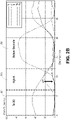
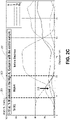
- FIG. 2B , FIG. 2C and 2D show energy-dispersive x-ray spectroscopy (EDX) line scans of a device with no nitrogen incorporation, a device with nitrogen doping and a device with plasma enhanced nitrogen implant.
- FIGS. 2B , 2C and 2D include plots with sections that correspond to the OEL 251, the high-k material 253 and the bottom electrode 255. Referring to FIGS. 2B and 2C , a comparison of the section of the plots that correspond to the high-k material 253 show an increased nitrogen concentration in the Ta 2 O 5 high-k film with nitrogen doping (see FIG. 2C arrow 258) as compared to the high-k film without doping (see FIG. 2B arrow 257). Referring to FIGS.
- EDX energy-dispersive x-ray spectroscopy
- the section of the plots that correspond to the high-k material 253 shows an increased nitrogen concentration in the Ta 2 O 5 high-k film with enhanced nitrogen implant ( FIG. 2D ) as compared to the high-k film with doping in ( FIG. 2C ).
- the arrow 259 points to a part of the plot that illustrates increased nitrogen concentration in the high-k material of the RRAM device.
- FIG. 2E shows a graph 260 of plots of example results from a low resistance state (LRS) retention test between RRAM devices without nitrogen incorporation into high-K and with N 2 plasma treatment.
- the RRAM devices are programmed to a low resistance state by increasing the SET voltage until the LRS read resistance (LRS resistance before being heated) is below a given verify level (VL). The RRAM devices are then heated at 185 degrees Celsius for 24 hours and the resistance is measured at the read voltage. In an embodiment, the resistance after being heated is compared to a reference resistance level (RL). In an embodiment, the RRAM devices that are programmed to LRS that experience a drift to a resistance level above the RL are considered to be retention failures. Referring to FIG.
- the post-bake resistance distribution for the group of devices with N 2 plasma treatment 261 is tighter than the group 263 with no treatment and has no devices with resistance greater than the RL. It should be noted that results shown in FIG. 2E are exemplary and in other embodiments other results can be provided.
- FIG. 3 is flowchart 300 of a method for forming an RRAM device with improved LRS retention according to an embodiment.
- the method includes at 301, forming a bottom electrode.
- 303 forming a high-k material on the bottom electrode.
- 305 forming a top electrode and forming a top contact on the top electrode.
- 307 forming an encapsulating layer of Al 2 O 3 that encapsulates the bottom electrode, the high-k material, the top electrode and the top contact.
- the high-k material is configured to store data.
- the encapsulating layer of Al 2 O 3 is formed to block moisture.
- a SiN film is formed on the encapsulating layer.
- an oxygen exchange layer (OEL) material is formed on the high-k material.
- a layer that includes a noble metal or alloy is formed under the encapsulating layer and the bottom electrode.
- Implementations of embodiments of the invention may be formed or carried out on a substrate, such as a semiconductor substrate.
- the semiconductor substrate may be a crystalline substrate formed using a bulk silicon or a silicon-on-insulator substructure.
- the semiconductor substrate may be formed using alternate materials, which may or may not be combined with silicon, that include but are not limited to germanium, indium antimonide, lead telluride, indium arsenide, indium phosphide, gallium arsenide, indium gallium arsenide, gallium antimonide, or other combinations of group III-V or group IV materials. Although a few examples of materials from which the substrate may be formed are described here, any material that may serve as a foundation upon which a semiconductor device may be built falls within the scope of the present invention.
- MOSFET metal-oxide-semiconductor field-effect transistors
- the MOS transistors may be planar transistors, nonplanar transistors, or a combination of both.
- Nonplanar transistors include FinFET transistors such as double-gate transistors and tri-gate transistors, and wrap-around or all-around gate transistors such as nanoribbon and nanowire transistors.
- Each MOS transistor includes a gate stack formed of at least two layers, a gate dielectric layer and a gate electrode layer.
- the gate dielectric layer may include one layer or a stack of layers.
- the one or more layers may include silicon oxide, silicon dioxide (SiO2) and/or a high-k dielectric material.
- the high-k dielectric material may include elements such as hafnium, silicon, oxygen, titanium, tantalum, lanthanum, aluminum, zirconium, barium, strontium, yttrium, lead, scandium, niobium, and zinc.
- high-k materials that may be used in the gate dielectric layer include, but are not limited to, hafnium oxide, hafnium silicon oxide, lanthanum oxide, lanthanum aluminum oxide, zirconium oxide, zirconium silicon oxide, tantalum oxide, titanium oxide, barium strontium titanium oxide, barium titanium oxide, strontium titanium oxide, yttrium oxide, aluminum oxide, lead scandium tantalum oxide, and lead zinc niobate.
- an annealing process may be carried out on the gate dielectric layer to improve its quality when a high-k material is used.
- the gate electrode layer is formed on the gate dielectric layer and may consist of at least one P-type workfunction metal or N-type workfunction metal, depending on whether the transistor is to be a PMOS or an NMOS transistor.
- the gate electrode layer may consist of a stack of two or more metal layers, where one or more metal layers are workfunction metal layers and at least one metal layer is a fill metal layer.
- metals that may be used for the gate electrode include, but are not limited to, ruthenium, palladium, platinum, cobalt, nickel, and conductive metal oxides, e.g., ruthenium oxide.
- a P-type metal layer will enable the formation of a PMOS gate electrode with a workfunction that is between about 4.9 eV and about 5.2 eV.
- metals that may be used for the gate electrode include, but are not limited to, hafnium, zirconium, titanium, tantalum, aluminum, alloys of these metals, and carbides of these metals such as hafnium carbide, zirconium carbide, titanium carbide, tantalum carbide, and aluminum carbide.
- An N-type metal layer will enable the formation of an NMOS gate electrode with a workfunction that is between about 3.9 eV and about 4.2 eV.
- the gate electrode may consist of a "U"-shaped structure that includes a bottom portion substantially parallel to the surface of the substrate and two sidewall portions that are substantially perpendicular to the top surface of the substrate.
- at least one of the metal layers that form the gate electrode may simply be a planar layer that is substantially parallel to the top surface of the substrate and does not include sidewall portions substantially perpendicular to the top surface of the substrate.
- the gate electrode may consist of a combination of U-shaped structures and planar, non-U-shaped structures.
- the gate electrode may consist of one or more U-shaped metal layers formed atop one or more planar, non-U-shaped layers.
- a pair of sidewall spacers may be formed on opposing sides of the gate stack that bracket the gate stack.
- the sidewall spacers may be formed from a material such as silicon nitride, silicon oxide, silicon carbide, silicon nitride doped with carbon, and silicon oxynitride. Processes for forming sidewall spacers are well known in the art and generally include deposition and etching process steps. In an alternate implementation, a plurality of spacer pairs may be used, for instance, two pairs, three pairs, or four pairs of sidewall spacers may be formed on opposing sides of the gate stack.
- source and drain regions are formed within the substrate adjacent to the gate stack of each MOS transistor.
- the source and drain regions are generally formed using either an implantation/diffusion process or an etching/deposition process.
- dopants such as boron, aluminum, antimony, phosphorous, or arsenic may be ion-implanted into the substrate to form the source and drain regions.
- An annealing process that activates the dopants and causes them to diffuse further into the substrate typically follows the ion implantation process.
- the substrate may first be etched to form recesses at the locations of the source and drain regions.
- the source and drain regions may be fabricated using a silicon alloy such as silicon germanium or silicon carbide.
- the epitaxially deposited silicon alloy may be doped in situ with dopants such as boron, arsenic, or phosphorous.
- the source and drain regions may be formed using one or more alternate semiconductor materials such as germanium or a group III-V material or alloy. And in further embodiments, one or more layers of metal and/or metal alloys may be used to form the source and drain regions.
- ILD interlayer dielectrics
- the ILD layers may be formed using dielectric materials known for their applicability in integrated circuit structures, such as low-k dielectric materials. Examples of dielectric materials that may be used include, but are not limited to, silicon dioxide (SiO2), carbon doped oxide (CDO), silicon nitride, organic polymers such as perfluorocyclobutane or polytetrafluoroethylene, fluorosilicate glass (FSG), and organosilicates such as silsesquioxane, siloxane, or organosilicate glass.
- the ILD layers may include pores or air gaps to further reduce their dielectric constant.
- FIG. 4 illustrates a computing device 400 in accordance with one embodiment.
- the computing device 400 houses a board 402.
- the board 402 may include a number of components, including but not limited to a processor 404 and at least one communication chip 406.
- the processor 404 is physically and electrically coupled to the board 402.
- the at least one communication chip 406 is also physically and electrically coupled to the board 402.
- the communication chip 406 is part of the processor 404.
- computing device 400 may include other components that may or may not be physically and electrically coupled to the board 402. These other components include, but are not limited to, volatile memory (e.g., DRAM), nonvolatile memory (e.g., ROM), flash memory, a graphics processor, a digital signal processor, a crypto processor, a chipset, an antenna, a display, a touchscreen display, a touchscreen controller, a battery, an audio codec, a video codec, a power amplifier, a global positioning system (GPS) device, a compass, an accelerometer, a gyroscope, a speaker, a camera, and a mass storage device (such as hard disk drive, compact disk (CD), digital versatile disk (DVD), and so forth).
- volatile memory e.g., DRAM
- nonvolatile memory e.g., ROM
- flash memory e.g., a graphics processor, a digital signal processor, a crypto processor, a chipset, an antenna, a display,
- the communication chip 406 enables wireless communications for the transfer of data to and from the computing device 400.
- wireless and its derivatives may be used to describe circuits, devices, systems, methods, techniques, communications channels, etc., that may communicate data through the use of modulated electromagnetic radiation through a non-solid medium. The term does not imply that the associated devices do not contain any wires, although in some embodiments they might not.
- the communication chip 406 may implement any of a number of wireless standards or protocols, including but not limited to Wi-Fi (IEEE 802.11 family), WiMAX (IEEE 802.16 family), IEEE 802.20, long term evolution (LTE), Ev-DO, HSPA+, HSDPA+, HSUPA+, EDGE, GSM, GPRS, CDMA, TDMA, DECT, Bluetooth, derivatives thereof, as well as any other wireless protocols that are designated as 3G, 4G, 5G, and beyond.
- the computing device 400 may include a plurality of communication chips 406.
- a first communication chip 406 may be dedicated to shorter range wireless communications such as Wi-Fi and Bluetooth and a second communication chip 406 may be dedicated to longer range wireless communications such as GPS, EDGE, GPRS, CDMA, WiMAX, LTE, Ev-DO, and others.
- the processor 404 of the computing device 400 includes an integrated circuit die packaged within the processor 404.
- the integrated circuit die of the processor includes one or more devices, such as MOS-FET transistors built in accordance with embodiments.
- the term "processor" may refer to any device or portion of a device that processes electronic data from registers and/or memory to transform that electronic data into other electronic data that may be stored in registers and/or memory.
- the communication chip 406 also includes an integrated circuit die packaged within the communication chip 406.
- the integrated circuit die of the communication chip includes one or more devices, such as MOS-FET transistors built in accordance with embodiments.
- another component housed within the computing device 400 may contain an integrated circuit die that includes one or more devices, such as MOS-FET transistors built in accordance with embodiments.
- the computing device 400 may be a laptop, a netbook, a notebook, an ultrabook, a smartphone, a tablet, a personal digital assistant (PDA), an ultra mobile PC, a mobile phone, a desktop computer, a server, a printer, a scanner, a monitor, a set-top box, an entertainment control unit, a digital camera, a portable music player, or a digital video recorder.
- the computing device 400 may be any other electronic device that processes data.
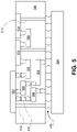
- FIG. 5 illustrates an interposer 500 that includes one or more embodiments of the invention.
- the interposer 500 is an intervening substrate used to bridge a first substrate 502 to a second substrate 504.
- the first substrate 502 may be, for instance, an integrated circuit die.
- the second substrate 504 may be, for instance, a memory module, a computer motherboard, or another integrated circuit die.
- the purpose of an interposer 500 is to spread a connection to a wider pitch or to reroute a connection to a different connection.
- an interposer 500 may couple an integrated circuit die to a ball grid array (BGA) 506 that can subsequently be coupled to the second substrate 504.
- BGA ball grid array
- the first and second substrates 502/504 are attached to opposing sides of the interposer 500.
- the first and second substrates 502/504 are attached to the same side of the interposer 500.
- three or more substrates are interconnected by way of the interposer 500.
- the interposer 500 may be formed of an epoxy resin, a fiberglass-reinforced epoxy resin, a ceramic material, or a polymer material such as polyimide.
- the interposer may be formed of alternate rigid or flexible materials that may include the same materials described above for use in a semiconductor substrate, such as silicon, germanium, and other group III-V and group IV materials.
- the interposer may include metal interconnects 508 and vias 510, including but not limited to through-silicon vias (TSVs) 512.
- the interposer 500 may further include embedded devices 514, including both passive and active devices. Such devices include, but are not limited to, capacitors, decoupling capacitors, resistors, inductors, fuses, diodes, transformers, sensors, and electrostatic discharge (ESD) devices. More complex devices such as radio-frequency (RF) devices, power amplifiers, power management devices, antennas, arrays, sensors, and MEMS devices may also be formed on the interposer 500.
- RF radio-frequency
- apparatuses or processes disclosed herein may be used in the fabrication of interposer 500.
Landscapes
- Engineering & Computer Science (AREA)
- Manufacturing & Machinery (AREA)
- Semiconductor Memories (AREA)
Abstract
Description
- Embodiments of the disclosure pertain to retention improvement of RRAM devices and, in particular, to retention improvement by high-k encapsulation of RRAM devices.
- RRAM, also known as ReRAM (resistive random access memory), is a form of nonvolatile data storage that operates by changing the resistance of a specially formulated solid dielectric material. An RRAM device contains a component called a memristor whose resistance varies when different voltages are imposed across it.
- Normally, a dielectric material does not conduct electric current. However, if the dielectric material is subjected to a high enough voltage, it will suddenly conduct because of dielectric breakdown. In a conventional dielectric material, dielectric breakdown causes permanent damage and failure of the associated component. In a memristor, the dielectric breakdown is temporary and reversible because of the materials that are used. In one form of memristor, a deliberately applied voltage causes the medium to acquire microscopic conductive paths called filaments. The filaments appear as a result of various phenomena such as metal migration or physical defects. Once a filament appears, it can be broken or reversed by the application of a different external voltage. The controlled formation and destruction of filaments in large numbers allows for storage of digital data. The voltage that is used initially to cause the medium to acquire the microscopic conductive paths is called the forming voltage.
- An RRAM device is placed in a low resistance state by applying a forming voltage that causes the dielectric to assume a resistance level that is below a given resistance threshold. RRAM devices that are in a low resistance state (LRS) that are exposed to moisture can exhibit retention failure. The retention failure is characterized by the drifting of bits in a low resistance state to a higher resistance than a given reference resistance level (RL).
- In a previous approach a transistor that is more powerful than is conventionally used is employed to generate high write currents in order to program devices into a LRS with a thicker filament. This approach oftentimes requires a larger transistor than is conventionally used. The larger transistors occupy more space and thus can result in reduced memory density. Moreover, the larger RRAM filaments that are formed can result in decreased endurance.
- Embodiments of the invention will now be described, by way of example only, with reference to the accompanying drawings in which:
-
FIG. 1A is an illustration of a cross-section of an RRAM device according to an embodiment. -
FIG. 1B is an illustration of a graph of plots from a low resistance state (LRS) retention test of devices with high-k encapsulation and without high-k encapsulation. -
FIG. 2A is an illustration of a cross-section of a RRAM device according to an embodiment. -
FIGS. 2B-2E are illustrations of energy-dispersive x-ray spectroscopy (EDX) line scans of a device with no nitrogen incorporation, a device with nitrogen doping and a device with a plasma enhanced nitrogen implant. -
FIG. 3 is a flowchart of a method for forming an RRAM device with improved LRS retention according to an embodiment. -
FIG. 4 illustrates a computing device in accordance with one implementation of an embodiment. -
FIG. 5 illustrates an interposer that includes one or more examples of an embodiment. - Various respective aspects and features of the invention are defined in the appended claims. Combinations of features from the dependent claims may be combined with features of the independent claims as appropriate and not merely as explicitly set out in the claims.
- RRAM retention improvement by high-k encapsulation of RRAM devices is described. It should be appreciated that although embodiments are described herein with reference to example high-k encapsulation of RRAM device implementations, the disclosure is more generally applicable to retention improvement by high-k encapsulation of RRAM device implementations as well as other type retention improvement by high-k encapsulation of RRAM device implementations. In the following description, numerous specific details are set forth, such as specific integration and material regimes, in order to provide a thorough understanding of embodiments of the present disclosure. It will be apparent to one skilled in the art that embodiments of the present disclosure may be practiced without these specific details. In other instances, well-known features, such as integrated circuit design layouts, are not described in detail in order to not unnecessarily obscure embodiments of the present disclosure. Furthermore, it is to be appreciated that the various embodiments shown in the Figures are illustrative representations and are not necessarily drawn to scale.
- Certain terminology may also be used in the following description for the purpose of reference only, and thus are not intended to be limiting. For example, terms such as "upper", "lower", "above", and "below" refer to directions in the drawings to which reference is made. Terms such as "front", "back", "rear", and "side" describe the orientation and/or location of portions of the component within a consistent but arbitrary frame of reference which is made clear by reference to the text and the associated drawings describing the component under discussion. Such terminology may include the words specifically mentioned above, derivatives thereof, and words of similar import.
- RRAM devices in the low resistance state (LRS) that are exposed to moisture can experience retention failure. The retention failure is characterized by the drifting of bits in a low resistance state to a resistance that is higher than a given reference resistance level (RL). In a previous approach to addressing retention failure, a transistor that is more powerful than is conventionally used is employed to generate high write currents in order to program devices into a LRS with a thicker filament. This approach oftentimes requires a larger transistor than is conventionally used. The larger transistors occupy more space and thus can result in reduced memory density. Moreover, the larger RRAM filaments can result in poor endurance.
- An approach that addresses the shortcomings of previous approaches is disclosed herein. For example, as part of a disclosed process the RRAM device is encapsulated with a thin aluminum oxide (Al2O3) layer that prevents moisture from penetrating the RRAM device. Preventing moisture from penetrating the RRAM device significantly improves LRS retention. In particular, the prevention of the penetration of moisture that is effected by the Al2O3 layer greatly reduces LRS drift to high resistance. This decreases the LRS failure rate by an order of magnitude. Moreover, the retention benefit does not come at the expense of yield or endurance.
- In addition, in an embodiment, nitrogen is incorporated into high-k tantalum oxide (Ta2O5) by exposing a blanket physical vapor deposition (PVD) Ta2O5 film to a N2 plasma. Nitrogen can also be doped into the high-k material using ion implantation. The incorporation of nitrogen into the high-k active layer significantly reduces retention failure from the drifting of devices from a low resistance state to a high resistance state. This retention benefit does not increase the set current that is needed for writing the device to LRS.
-
FIG. 1A is an illustration of a cross-section of anRRAM device 100 according to an embodiment.FIG. 1A showsbottom electrode 101,bottom electrode 103, high-k material 105, oxygen exchange layer (OEL) 107,top electrode 109,top contact 111, Al2O3 layer 113,SiN 115,barrier layer 117 andbit line contact 119. - Referring to
FIG. 1A , thebottom electrode 103 is formed on thebottom electrode 101. The high-k material 105 is formed onbottom electrode 103. TheOEL 107 is formed on the high-k material 105. Thetop electrode 109 is formed on theOEL 107. Thetop contact 111 is formed on thetop electrode 109. The Al2O3 layer 113 encapsulates thebottom electrode 103, the high-k material 105, theOEL 107, thetop electrode 109, and thetop contact 111. TheSiN 115 is formed on the Al2O3 layer 113. Thebit line contact 119 is formed in the space formed by thebit line contact 119. - In an embodiment, the
bottom electrode 101 can be formed from a noble metal or alloy (TiN, WN, Pt, Ru, Ir or TaN). In other embodiments, thebottom electrode 101 can be formed from other materials. In an embodiment, thebottom electrode 103 can be formed from noble metal or alloy. In other embodiments, thebottom electrode 103 can be formed from other materials. In an embodiment, the high-k material 105 can be formed from HfO, TaO, ZrO or SiO. In other embodiments, the high-k material 105 can be formed from other materials. In an embodiment, theOEL layer 107 can be formed from a reactive metal (e.g., can use metal corresponding to high-k material Hf, Ta, Zr, Ti etc.). In other embodiments, theOEL layer 107 can be formed from other materials. In an embodiment, thetop electrode 109 can be formed from TiN, WN, Pt, Ru, Ir or TaN. In other embodiments, the top electrode109 can be formed from other materials. In an embodiment, thetop contact 111 can be formed from Ta or W. In other embodiments, thetop contact 111 can be formed from other materials. In an embodiment, thebarrier layer 117 can be formed from Ta. In other embodiments, thebarrier layer 117 can be formed from other material. In an embodiment,bit line contact 119 can be formed from copper. In other embodiments,bit line contact 119 be formed from other materials. - In operation, when a set voltage is applied to the memory cell, a low resistance filament is created and the device is placed into a low resistance state. It should be appreciated that the set voltage causes the diffusion of oxygen from the high-
k layer 105 into theOEL layer 107 to create the low resistance filament in the high-k material. The filament is characterized by oxygen vacancies. In an embodiment, a penetration of moisture into the high-k material can degrade the filament by causing the diffusion of oxygen vacancy eliminating oxygen atoms into the high-k dielectric. The degradation of the low resistance filament in this manner can cause the resistance of the high-k material to drift higher. Thus, the prevention of moisture from penetrating into the high-k dielectric can prevent a LRS drift of the resistance and significantly improve LRS retention. In an embodiment, moisture is prevented from diffusing into the low-k dielectric by the Al2O3 layer. In an embodiment, this can decrease the LRS failure rate by an order of magnitude. Moreover, the retention benefit does not come at the expense of yield or endurance. - It should be appreciated that the setting and resetting of the
RRAM device 100 requires a certain level of oxygen atoms that can be removed from, and returned to, the high-k material in order to sufficiently change its resistance level from one resistance state to the other. The loss of oxygen atoms from theRRAM device 100 can cause a loss of the ability to reset the device by controlling the diffusion of oxygen into and out of the high-k material 105. Thus, without a mechanism to retain oxygen in theRRAM device 100, the ability to reset the device can be lost after a number of cycles. The number of cycles that it takes to reach this point is referred to as endurance. In an embodiment, the Al2O3 layer 113 prevents oxygen atoms from escaping theRRAM device 100. Thus, in an embodiment, endurance is increased as the Al2O3 layer 113 slows the escape of oxygen from the device. In other embodiments, other materials can be used to prevent the loss of oxygen from theRRAM device 100. - In an embodiment, the
RRAM device 100 can be formed on blanket RRAM films using lithography. In an embodiment, dry etching can be used to transfer a photomask pattern to underlying RRAM films. In other embodiments, other manner of transferring the photomask pattern can be used. The structure can then be encapsulated with an atomic layer deposition (ALD) aluminum oxide (Al2O3) and CVD SiN film. The Al2O3 film acts as a hermetic barrier to the diffusion of moisture into the high-k active layer of theRRAM device 100. As described herein, the reduced moisture content reduces oxygen diffusion into the device and improves retention of the low resistance state (LRS). Thus, in an embodiment, the Al2O3 encapsulation significantly reduces retention failures by decreasing the drift of the low resistance state (LRS) to resistances above the reference level (RL). -
FIG. 1B shows agraph 150 of plots from a LRS retention test of devices with Al2O3 encapsulation 151 and without high-k encapsulation 153. Both of the device types represented in the retention plots ofFIG. 1B , have a SiN encapsulation layer (e.g., 115 inFIG. 1A ). In an embodiment, both device types are programmed to a low resistance state by increasing a SET voltage until the LRS read resistance (LRS resistance before being heated) is below a resistance verify level (VL). The devices are then heated at 185 degrees Celsius for 24 hours whereupon the resistance is measured at the read voltage. The post bake resistance is compared to a reference resistance level (RL). Devices programmed to the LRS which drift to a resistance level above the RL are considered retention failures. Referring toFIG. 1B , the post-bake resistance distribution for the group of devices with Al2O3 encapsulation is tighter than the group with no high-k encapsulation. It should be appreciated that the results shown inFIG. 1B are exemplary and in other embodiments other results can be provided. -
FIG. 2A is an illustration of a cross-section of aRRAM device 200 according to an embodiment.FIG. 2A showsbottom electrode 201,bottom electrode 203,high k material 205, oxygen exchange layer (OEL) 207,top electrode 209,top contact 211, Al2O3 layer 213,SiN 215,barrier layer 217 andbit line contact 219. These structures are similar to those of theRRAM device 100 shown inFIG. 1A and thus are not described again here for purposes of clarity and brevity. In an embodiment, in addition to the structures ofRRAM device 100 shown inFIG. 1A ,RRAM device 200 includes a high-kactive layer 205 that is doped with nitrogen. - Referring to
FIG. 2A , the stoichiometric Ta2O5 high-k film 205, which serves as the active layer for theRRAM device 200, is doped with nitrogen either by exposure to an N2 plasma or an N implant process. In an embodiment, theRRAM device 200 can be doped with nitrogen after the deposition of the Ta2O5 high-k film 205. In an embodiment, the nitrogen is substitutionally incorporated into the Ta2O5 lattice displacing oxygen in the film. The N2 plasma treatment significantly reduces retention failures by decreasing the drift of a low resistance state (LRS) resistance to resistances above the reference level (RL). - In operation, the incorporation of nitrogen into the high-k
active layer 205 theRRAM device 200 significantly improves LRS retention. In particular, the incorporation of nitrogen into the high-k active layer significantly reduces retention failure from the drifting of devices from a low resistance state to a high resistance state. This retention benefit does not increase the set current that is needed for writing the device to LRS. -
FIG. 2B ,FIG. 2C and2D show energy-dispersive x-ray spectroscopy (EDX) line scans of a device with no nitrogen incorporation, a device with nitrogen doping and a device with plasma enhanced nitrogen implant.FIGS. 2B ,2C and2D include plots with sections that correspond to theOEL 251, the high-k material 253 and thebottom electrode 255. Referring toFIGS. 2B and2C , a comparison of the section of the plots that correspond to the high-k material 253 show an increased nitrogen concentration in the Ta2O5 high-k film with nitrogen doping (seeFIG. 2C arrow 258) as compared to the high-k film without doping (seeFIG. 2B arrow 257). Referring toFIGS. 2C and2D , the section of the plots that correspond to the high-k material 253 shows an increased nitrogen concentration in the Ta2O5 high-k film with enhanced nitrogen implant (FIG. 2D ) as compared to the high-k film with doping in (FIG. 2C ). InFIG. 2D thearrow 259 points to a part of the plot that illustrates increased nitrogen concentration in the high-k material of the RRAM device. -
FIG. 2E shows agraph 260 of plots of example results from a low resistance state (LRS) retention test between RRAM devices without nitrogen incorporation into high-K and with N2 plasma treatment. In an embodiment, the RRAM devices are programmed to a low resistance state by increasing the SET voltage until the LRS read resistance (LRS resistance before being heated) is below a given verify level (VL). The RRAM devices are then heated at 185 degrees Celsius for 24 hours and the resistance is measured at the read voltage. In an embodiment, the resistance after being heated is compared to a reference resistance level (RL). In an embodiment, the RRAM devices that are programmed to LRS that experience a drift to a resistance level above the RL are considered to be retention failures. Referring toFIG. 2E , the post-bake resistance distribution for the group of devices with N2 plasma treatment 261 is tighter than thegroup 263 with no treatment and has no devices with resistance greater than the RL. It should be noted that results shown inFIG. 2E are exemplary and in other embodiments other results can be provided. -
FIG. 3 isflowchart 300 of a method for forming an RRAM device with improved LRS retention according to an embodiment. Referring toFIG. 3 , the method includes at 301, forming a bottom electrode. At 303, forming a high-k material on the bottom electrode. At 305, forming a top electrode and forming a top contact on the top electrode. At 307, forming an encapsulating layer of Al2O3 that encapsulates the bottom electrode, the high-k material, the top electrode and the top contact. In an embodiment, the high-k material is configured to store data. In an embodiment, the encapsulating layer of Al2O3 is formed to block moisture. In an embodiment, a SiN film is formed on the encapsulating layer. In an embodiment, an oxygen exchange layer (OEL) material is formed on the high-k material. In an embodiment, a layer that includes a noble metal or alloy is formed under the encapsulating layer and the bottom electrode. - Implementations of embodiments of the invention may be formed or carried out on a substrate, such as a semiconductor substrate. In one implementation, the semiconductor substrate may be a crystalline substrate formed using a bulk silicon or a silicon-on-insulator substructure. In other implementations, the semiconductor substrate may be formed using alternate materials, which may or may not be combined with silicon, that include but are not limited to germanium, indium antimonide, lead telluride, indium arsenide, indium phosphide, gallium arsenide, indium gallium arsenide, gallium antimonide, or other combinations of group III-V or group IV materials. Although a few examples of materials from which the substrate may be formed are described here, any material that may serve as a foundation upon which a semiconductor device may be built falls within the scope of the present invention.
- A plurality of transistors, such as metal-oxide-semiconductor field-effect transistors (MOSFET or simply MOS transistors), may be fabricated on the substrate. In various embodiments, the MOS transistors may be planar transistors, nonplanar transistors, or a combination of both. Nonplanar transistors include FinFET transistors such as double-gate transistors and tri-gate transistors, and wrap-around or all-around gate transistors such as nanoribbon and nanowire transistors. Although the implementations described herein may illustrate only planar transistors, it should be noted that embodiments of the invention may also be carried out using nonplanar transistors.
- Each MOS transistor includes a gate stack formed of at least two layers, a gate dielectric layer and a gate electrode layer. The gate dielectric layer may include one layer or a stack of layers. The one or more layers may include silicon oxide, silicon dioxide (SiO2) and/or a high-k dielectric material. The high-k dielectric material may include elements such as hafnium, silicon, oxygen, titanium, tantalum, lanthanum, aluminum, zirconium, barium, strontium, yttrium, lead, scandium, niobium, and zinc. Examples of high-k materials that may be used in the gate dielectric layer include, but are not limited to, hafnium oxide, hafnium silicon oxide, lanthanum oxide, lanthanum aluminum oxide, zirconium oxide, zirconium silicon oxide, tantalum oxide, titanium oxide, barium strontium titanium oxide, barium titanium oxide, strontium titanium oxide, yttrium oxide, aluminum oxide, lead scandium tantalum oxide, and lead zinc niobate. In some embodiments, an annealing process may be carried out on the gate dielectric layer to improve its quality when a high-k material is used.
- The gate electrode layer is formed on the gate dielectric layer and may consist of at least one P-type workfunction metal or N-type workfunction metal, depending on whether the transistor is to be a PMOS or an NMOS transistor. In some implementations, the gate electrode layer may consist of a stack of two or more metal layers, where one or more metal layers are workfunction metal layers and at least one metal layer is a fill metal layer.
- For a PMOS transistor, metals that may be used for the gate electrode include, but are not limited to, ruthenium, palladium, platinum, cobalt, nickel, and conductive metal oxides, e.g., ruthenium oxide. A P-type metal layer will enable the formation of a PMOS gate electrode with a workfunction that is between about 4.9 eV and about 5.2 eV. For an NMOS transistor, metals that may be used for the gate electrode include, but are not limited to, hafnium, zirconium, titanium, tantalum, aluminum, alloys of these metals, and carbides of these metals such as hafnium carbide, zirconium carbide, titanium carbide, tantalum carbide, and aluminum carbide. An N-type metal layer will enable the formation of an NMOS gate electrode with a workfunction that is between about 3.9 eV and about 4.2 eV.
- In some implementations, the gate electrode may consist of a "U"-shaped structure that includes a bottom portion substantially parallel to the surface of the substrate and two sidewall portions that are substantially perpendicular to the top surface of the substrate. In another implementation, at least one of the metal layers that form the gate electrode may simply be a planar layer that is substantially parallel to the top surface of the substrate and does not include sidewall portions substantially perpendicular to the top surface of the substrate. In further embodiments, the gate electrode may consist of a combination of U-shaped structures and planar, non-U-shaped structures. For example, the gate electrode may consist of one or more U-shaped metal layers formed atop one or more planar, non-U-shaped layers.
- In some embodiments, a pair of sidewall spacers may be formed on opposing sides of the gate stack that bracket the gate stack. The sidewall spacers may be formed from a material such as silicon nitride, silicon oxide, silicon carbide, silicon nitride doped with carbon, and silicon oxynitride. Processes for forming sidewall spacers are well known in the art and generally include deposition and etching process steps. In an alternate implementation, a plurality of spacer pairs may be used, for instance, two pairs, three pairs, or four pairs of sidewall spacers may be formed on opposing sides of the gate stack.
- As is well known in the art, source and drain regions are formed within the substrate adjacent to the gate stack of each MOS transistor. The source and drain regions are generally formed using either an implantation/diffusion process or an etching/deposition process. In the former process, dopants such as boron, aluminum, antimony, phosphorous, or arsenic may be ion-implanted into the substrate to form the source and drain regions. An annealing process that activates the dopants and causes them to diffuse further into the substrate typically follows the ion implantation process. In the latter process, the substrate may first be etched to form recesses at the locations of the source and drain regions. An epitaxial deposition process may then be carried out to fill the recesses with material that is used to fabricate the source and drain regions. In some implementations, the source and drain regions may be fabricated using a silicon alloy such as silicon germanium or silicon carbide. In some implementations the epitaxially deposited silicon alloy may be doped in situ with dopants such as boron, arsenic, or phosphorous. In further embodiments, the source and drain regions may be formed using one or more alternate semiconductor materials such as germanium or a group III-V material or alloy. And in further embodiments, one or more layers of metal and/or metal alloys may be used to form the source and drain regions.
- One or more interlayer dielectrics (ILD) are deposited over the MOS transistors. The ILD layers may be formed using dielectric materials known for their applicability in integrated circuit structures, such as low-k dielectric materials. Examples of dielectric materials that may be used include, but are not limited to, silicon dioxide (SiO2), carbon doped oxide (CDO), silicon nitride, organic polymers such as perfluorocyclobutane or polytetrafluoroethylene, fluorosilicate glass (FSG), and organosilicates such as silsesquioxane, siloxane, or organosilicate glass. The ILD layers may include pores or air gaps to further reduce their dielectric constant.
-
FIG. 4 illustrates acomputing device 400 in accordance with one embodiment. Thecomputing device 400 houses aboard 402. Theboard 402 may include a number of components, including but not limited to aprocessor 404 and at least onecommunication chip 406. Theprocessor 404 is physically and electrically coupled to theboard 402. In some implementations the at least onecommunication chip 406 is also physically and electrically coupled to theboard 402. In further implementations, thecommunication chip 406 is part of theprocessor 404. - Depending on its applications,
computing device 400 may include other components that may or may not be physically and electrically coupled to theboard 402. These other components include, but are not limited to, volatile memory (e.g., DRAM), nonvolatile memory (e.g., ROM), flash memory, a graphics processor, a digital signal processor, a crypto processor, a chipset, an antenna, a display, a touchscreen display, a touchscreen controller, a battery, an audio codec, a video codec, a power amplifier, a global positioning system (GPS) device, a compass, an accelerometer, a gyroscope, a speaker, a camera, and a mass storage device (such as hard disk drive, compact disk (CD), digital versatile disk (DVD), and so forth). - The
communication chip 406 enables wireless communications for the transfer of data to and from thecomputing device 400. The term "wireless" and its derivatives may be used to describe circuits, devices, systems, methods, techniques, communications channels, etc., that may communicate data through the use of modulated electromagnetic radiation through a non-solid medium. The term does not imply that the associated devices do not contain any wires, although in some embodiments they might not. Thecommunication chip 406 may implement any of a number of wireless standards or protocols, including but not limited to Wi-Fi (IEEE 802.11 family), WiMAX (IEEE 802.16 family), IEEE 802.20, long term evolution (LTE), Ev-DO, HSPA+, HSDPA+, HSUPA+, EDGE, GSM, GPRS, CDMA, TDMA, DECT, Bluetooth, derivatives thereof, as well as any other wireless protocols that are designated as 3G, 4G, 5G, and beyond. Thecomputing device 400 may include a plurality ofcommunication chips 406. For instance, afirst communication chip 406 may be dedicated to shorter range wireless communications such as Wi-Fi and Bluetooth and asecond communication chip 406 may be dedicated to longer range wireless communications such as GPS, EDGE, GPRS, CDMA, WiMAX, LTE, Ev-DO, and others. - The
processor 404 of thecomputing device 400 includes an integrated circuit die packaged within theprocessor 404. In some embodiments, the integrated circuit die of the processor includes one or more devices, such as MOS-FET transistors built in accordance with embodiments. The term "processor" may refer to any device or portion of a device that processes electronic data from registers and/or memory to transform that electronic data into other electronic data that may be stored in registers and/or memory. - The
communication chip 406 also includes an integrated circuit die packaged within thecommunication chip 406. In accordance with another implementation of the invention, the integrated circuit die of the communication chip includes one or more devices, such as MOS-FET transistors built in accordance with embodiments. - In further implementations, another component housed within the
computing device 400 may contain an integrated circuit die that includes one or more devices, such as MOS-FET transistors built in accordance with embodiments. - In various implementations, the
computing device 400 may be a laptop, a netbook, a notebook, an ultrabook, a smartphone, a tablet, a personal digital assistant (PDA), an ultra mobile PC, a mobile phone, a desktop computer, a server, a printer, a scanner, a monitor, a set-top box, an entertainment control unit, a digital camera, a portable music player, or a digital video recorder. In further implementations, thecomputing device 400 may be any other electronic device that processes data. -
FIG. 5 illustrates aninterposer 500 that includes one or more embodiments of the invention. Theinterposer 500 is an intervening substrate used to bridge afirst substrate 502 to asecond substrate 504. Thefirst substrate 502 may be, for instance, an integrated circuit die. Thesecond substrate 504 may be, for instance, a memory module, a computer motherboard, or another integrated circuit die. Generally, the purpose of aninterposer 500 is to spread a connection to a wider pitch or to reroute a connection to a different connection. For example, aninterposer 500 may couple an integrated circuit die to a ball grid array (BGA) 506 that can subsequently be coupled to thesecond substrate 504. In some embodiments, the first andsecond substrates 502/504 are attached to opposing sides of theinterposer 500. In other embodiments, the first andsecond substrates 502/504 are attached to the same side of theinterposer 500. And in further embodiments, three or more substrates are interconnected by way of theinterposer 500. - The
interposer 500 may be formed of an epoxy resin, a fiberglass-reinforced epoxy resin, a ceramic material, or a polymer material such as polyimide. In further implementations, the interposer may be formed of alternate rigid or flexible materials that may include the same materials described above for use in a semiconductor substrate, such as silicon, germanium, and other group III-V and group IV materials. - The interposer may include
metal interconnects 508 and vias 510, including but not limited to through-silicon vias (TSVs) 512. Theinterposer 500 may further include embeddeddevices 514, including both passive and active devices. Such devices include, but are not limited to, capacitors, decoupling capacitors, resistors, inductors, fuses, diodes, transformers, sensors, and electrostatic discharge (ESD) devices. More complex devices such as radio-frequency (RF) devices, power amplifiers, power management devices, antennas, arrays, sensors, and MEMS devices may also be formed on theinterposer 500. In accordance with embodiments of the invention, apparatuses or processes disclosed herein may be used in the fabrication ofinterposer 500. - Although specific embodiments have been described above, these embodiments are not intended to limit the scope of the present disclosure, even where only a single embodiment is described with respect to a particular feature. Examples of features provided in the disclosure are intended to be illustrative rather than restrictive unless stated otherwise. The above description is intended to cover such alternatives, modifications, and equivalents as would be apparent to a person skilled in the art having the benefit of the present disclosure.
- The scope of the present disclosure includes any feature or combination of features disclosed herein (either explicitly or implicitly), or any generalization thereof, whether or not it mitigates any or all of the problems addressed herein. Accordingly, new claims may be formulated during prosecution of the present application (or an application claiming priority thereto) to any such combination of features. In particular, with reference to the appended claims, features from dependent claims may be combined with those of the independent claims and features from respective independent claims may be combined in any appropriate manner and not merely in the specific combinations enumerated in the appended claims.
- The following examples pertain to further embodiments. The various features of the different embodiments may be variously combined with some features included and others excluded to suit a variety of different applications.
- Example embodiment 1: An RRAM device, including a bottom electrode, a high-k material on the bottom electrode, a top electrode; a top contact on the top electrode, and an encapsulating layer of Al2O3 that encapsulates the bottom electrode, the high-k material, the top electrode and the top contact.
- Example embodiment 2: The RRAM device of
example embodiment 1, wherein the high-k material is configured to store data. - Example embodiment 3: The RRAM device of
example embodiment 1, wherein the encapsulating layer of Al2O3 is configured to block moisture. - Example embodiment 4: The RRAM device of
example embodiment 1, further comprising SiN film formed on the encapsulating layer. - Example embodiment 5: The RRAM device of
example embodiment 1, further comprising an oxygen exchange layer (OEL) material on the high-k material. - Example embodiment 6: The RRAM device of
example embodiment 1, further comprising a layer that includes a noble metal or alloy under the encapsulating layer and the bottom electrode. - Example embodiment 7: The RRAM device of
example embodiment - Example embodiment 8: An RRAM device, including a bottom electrode, a high-k material including Ta2O5 doped with nitrogen on the bottom electrode, a top electrode, a top contact on the top electrode, and an encapsulating layer of Al2O3 that encapsulates the bottom electrode, the high-k material, the top electrode and the top contact.
- Example embodiment 9: The RRAM device of example embodiment 8, wherein the high-k material is configured to store data.
- Example embodiment 10: The RRAM device of example embodiment 8, wherein the encapsulating layer of Al2O3 is configured to block moisture.
- Example embodiment 11: The RRAM device of example embodiment 8, further comprising SiN film formed on the encapsulating layer.
- Example embodiment 12: The RRAM device of example embodiment 8, further comprising an oxygen exchange layer (OEL) material on the high-k material.
- Example embodiment 13: The RRAM device of example embodiment 8, further comprising a layer that includes a noble metal or alloy under the encapsulating layer and the bottom electrode.
- Example embodiment 14: The RRAM device of
example embodiment 8, 9, 10, 11, 12 or 13 further comprising a bit line contact coupled to the top electrode. - Example embodiment 15: A method, including forming a bottom electrode, forming a high-k material on the bottom electrode; forming a top electrode, forming a top contact on the top electrode, and forming an encapsulating layer of Al2O3 that encapsulates the bottom electrode, the high-k material, the top electrode and the top contact.
- Example embodiment 16: The method of
example embodiment 15, wherein the high-k material is configured to store data. - Example embodiment 17: The method of
example embodiment 15, wherein forming the encapsulating layer of Al2O3 includes forming the encapsulating layer of Al2O3 to block moisture. - Example embodiment 18: The method of
example embodiment 15, further comprising forming SiN film on the encapsulating layer. - Example embodiment 19: The method of
example embodiment 15, further comprising forming an oxygen exchange layer (OEL) material on the high-k material. - Example embodiment 20: The method of
example embodiment 15, 16, 17, 18 or 19 further comprising forming a layer that includes a noble metal or alloy under the encapsulating layer and the bottom electrode.
Claims (13)
- An RRAM device, comprising:a bottom electrode;a high-k material on the bottom electrode;a top electrode;a top contact on the top electrode; andan encapsulating layer of Al2O3 that encapsulates the bottom electrode, the high-k material, the top electrode and the top contact.
- The RRAM device of claim 1, wherein the high-k material is configured to store data.
- The RRAM device of claim 1 or 2, wherein the encapsulating layer of Al2O3 is configured to block moisture.
- The RRAM device of claim 1, 2 or 3, further comprising SiN film formed on the encapsulating layer.
- The RRAM device of claim 1, 2, 3 or 4, further comprising an oxygen exchange layer (OEL) material on the high-k material.
- The RRAM device of claim 1, 2, 3, 4, 5 or 6, further comprising a layer including a noble metal or alloy under the encapsulating layer and the bottom electrode.
- The RRAM device of claim 1, 2, 3, 4, 5 or 6, further comprising a bit line contact coupled to the top electrode.
- A method, comprising:forming a bottom electrode;forming a high-k material on the bottom electrode;forming a top electrode;forming a top contact on the top electrode; andforming an encapsulating layer of Al2O3 that encapsulates the bottom electrode, the high-k material, the top electrode and the top contact.
- The method of claim 8, wherein the high-k material is configured to store data.
- The method of claim 8 or 9, wherein forming the encapsulating layer of Al2O3 includes forming the encapsulating layer of Al2O3 to block moisture.
- The method of claim 8, 9 or 10, further comprising forming SiN film on the encapsulating layer.
- The method of claim 8, 9, 10 or 11, further comprising forming an oxygen exchange layer (OEL) material on the high-k material.
- The method of claim 8, 9, 10, 11 or 12, further comprising forming a layer that includes a noble metal or alloy under the encapsulating layer and the bottom electrode.
Applications Claiming Priority (2)
| Application Number | Priority Date | Filing Date | Title |
|---|---|---|---|
| US16/226,198 US11462684B2 (en) | 2018-12-19 | 2018-12-19 | Retention improvement by high-k encapsulation of RRAM devices |
| EP19209848.1A EP3671875B1 (en) | 2018-12-19 | 2019-11-18 | Retention improvement of rram devices by high-k encapsulation |
Related Parent Applications (2)
| Application Number | Title | Priority Date | Filing Date |
|---|---|---|---|
| EP19209848.1A Division EP3671875B1 (en) | 2018-12-19 | 2019-11-18 | Retention improvement of rram devices by high-k encapsulation |
| EP19209848.1A Division-Into EP3671875B1 (en) | 2018-12-19 | 2019-11-18 | Retention improvement of rram devices by high-k encapsulation |
Publications (2)
| Publication Number | Publication Date |
|---|---|
| EP3979347A1 true EP3979347A1 (en) | 2022-04-06 |
| EP3979347B1 EP3979347B1 (en) | 2025-04-02 |
Family
ID=68610066
Family Applications (2)
| Application Number | Title | Priority Date | Filing Date |
|---|---|---|---|
| EP19209848.1A Active EP3671875B1 (en) | 2018-12-19 | 2019-11-18 | Retention improvement of rram devices by high-k encapsulation |
| EP21208003.0A Active EP3979347B1 (en) | 2018-12-19 | 2019-11-18 | Retention improvement of rram devices by high-k encapsulation |
Family Applications Before (1)
| Application Number | Title | Priority Date | Filing Date |
|---|---|---|---|
| EP19209848.1A Active EP3671875B1 (en) | 2018-12-19 | 2019-11-18 | Retention improvement of rram devices by high-k encapsulation |
Country Status (2)
| Country | Link |
|---|---|
| US (1) | US11462684B2 (en) |
| EP (2) | EP3671875B1 (en) |
Citations (5)
| Publication number | Priority date | Publication date | Assignee | Title |
|---|---|---|---|---|
| US20060054950A1 (en) * | 2004-09-10 | 2006-03-16 | In-Gyu Baek | Non-volatile memory cells employing a transition metal oxide layer as a data storage material layer and methods of manufacturing the same |
| US20110291066A1 (en) * | 2010-06-01 | 2011-12-01 | In-Gyu Baek | Nonvolatile Memory Devices Having Cells with Oxygen Diffusion Barrier Layers Therein and Methods of Manufacturing the Same |
| US20140097396A1 (en) * | 2012-09-26 | 2014-04-10 | Panasonic Corporation | Non-volatile memory device and manufacturing method thereof |
| US20140252298A1 (en) * | 2013-03-10 | 2014-09-11 | Sandisk 3D Llc | Methods and apparatus for metal oxide reversible resistance-switching memory devices |
| US20150171142A1 (en) * | 2013-12-16 | 2015-06-18 | Panasonic Intellectual Property Management Co., Ltd. | Nonvolatile memory device and method for manufacturing the same |
Family Cites Families (2)
| Publication number | Priority date | Publication date | Assignee | Title |
|---|---|---|---|---|
| TWI610476B (en) * | 2017-03-16 | 2018-01-01 | 華邦電子股份有限公司 | Resistive random access memory structure and forming method thereof |
| WO2018214142A1 (en) * | 2017-05-26 | 2018-11-29 | 中国科学院微电子研究所 | Resistive memory device, and manufacturing method thereof |
-
2018
- 2018-12-19 US US16/226,198 patent/US11462684B2/en active Active
-
2019
- 2019-11-18 EP EP19209848.1A patent/EP3671875B1/en active Active
- 2019-11-18 EP EP21208003.0A patent/EP3979347B1/en active Active
Patent Citations (5)
| Publication number | Priority date | Publication date | Assignee | Title |
|---|---|---|---|---|
| US20060054950A1 (en) * | 2004-09-10 | 2006-03-16 | In-Gyu Baek | Non-volatile memory cells employing a transition metal oxide layer as a data storage material layer and methods of manufacturing the same |
| US20110291066A1 (en) * | 2010-06-01 | 2011-12-01 | In-Gyu Baek | Nonvolatile Memory Devices Having Cells with Oxygen Diffusion Barrier Layers Therein and Methods of Manufacturing the Same |
| US20140097396A1 (en) * | 2012-09-26 | 2014-04-10 | Panasonic Corporation | Non-volatile memory device and manufacturing method thereof |
| US20140252298A1 (en) * | 2013-03-10 | 2014-09-11 | Sandisk 3D Llc | Methods and apparatus for metal oxide reversible resistance-switching memory devices |
| US20150171142A1 (en) * | 2013-12-16 | 2015-06-18 | Panasonic Intellectual Property Management Co., Ltd. | Nonvolatile memory device and method for manufacturing the same |
Also Published As
| Publication number | Publication date |
|---|---|
| US11462684B2 (en) | 2022-10-04 |
| EP3979347B1 (en) | 2025-04-02 |
| EP3671875A1 (en) | 2020-06-24 |
| EP3671875B1 (en) | 2022-07-06 |
| US20200203605A1 (en) | 2020-06-25 |
Similar Documents
| Publication | Publication Date | Title |
|---|---|---|
| US11342499B2 (en) | RRAM devices with reduced forming voltage | |
| US11621395B2 (en) | Resistive random-access memory devices and methods of fabrication | |
| US11901400B2 (en) | MFM capacitor and process for forming such | |
| US10868246B2 (en) | Conductive bridge random access memory (CBRAM) devices with low thermal conductivity electrolyte sublayer | |
| US11430948B2 (en) | Resistive random access memory device with switching multi-layer stack and methods of fabrication | |
| US11264317B2 (en) | Antifuse memory arrays with antifuse elements at the back-end-of-line (BEOL) | |
| US11631717B2 (en) | 3D memory array with memory cells having a 3D selector and a storage component | |
| US11171145B2 (en) | Memory devices based on capacitors with built-in electric field | |
| US11690215B2 (en) | Self-aligned bitline and capacitor via formation | |
| US11594533B2 (en) | Stacked trigate transistors with dielectric isolation between first and second semiconductor fins | |
| US11189564B2 (en) | Metal-oxide-semiconductor field-effect-transistors (MOSFET) as antifuse elements | |
| WO2018004588A1 (en) | Approaches for fabricating back end of line (beol)-compatible rram devices and the resulting structures | |
| US11488978B2 (en) | Ferroelectric gate oxide based tunnel feFET memory | |
| EP3716300B1 (en) | Mfm capacitor with multilayered oxides and metals and processes for forming such | |
| US11908911B2 (en) | Thin film transistors with raised source and drain contacts and process for forming such | |
| US11967615B2 (en) | Dual threshold voltage (VT) channel devices and their methods of fabrication | |
| US20220254931A1 (en) | Thin film transistor including a dielectric diffusion barrier and methods for forming the same | |
| US11923290B2 (en) | Halogen treatment for NMOS contact resistance improvement | |
| US11462684B2 (en) | Retention improvement by high-k encapsulation of RRAM devices | |
| WO2018004562A1 (en) | Approaches for fabricating self-aligned pedestals for rram devices and the resulting structures | |
| US11417705B2 (en) | RRAM memory cell and process to increase RRAM material area in an RRAM memory cell | |
| US12142689B2 (en) | Transistor including wrap around source and drain contacts | |
| WO2019059892A1 (en) | Metallic glass barriers for electrodes and contacts in semiconductor devices |
Legal Events
| Date | Code | Title | Description |
|---|---|---|---|
| PUAI | Public reference made under article 153(3) epc to a published international application that has entered the european phase |
Free format text: ORIGINAL CODE: 0009012 |
|
| STAA | Information on the status of an ep patent application or granted ep patent |
Free format text: STATUS: THE APPLICATION HAS BEEN PUBLISHED |
|
| AC | Divisional application: reference to earlier application |
Ref document number: 3671875 Country of ref document: EP Kind code of ref document: P |
|
| AK | Designated contracting states |
Kind code of ref document: A1 Designated state(s): AL AT BE BG CH CY CZ DE DK EE ES FI FR GB GR HR HU IE IS IT LI LT LU LV MC MK MT NL NO PL PT RO RS SE SI SK SM TR |
|
| STAA | Information on the status of an ep patent application or granted ep patent |
Free format text: STATUS: REQUEST FOR EXAMINATION WAS MADE |
|
| 17P | Request for examination filed |
Effective date: 20220901 |
|
| RBV | Designated contracting states (corrected) |
Designated state(s): AL AT BE BG CH CY CZ DE DK EE ES FI FR GB GR HR HU IE IS IT LI LT LU LV MC MK MT NL NO PL PT RO RS SE SI SK SM TR |
|
| REG | Reference to a national code |
Ref country code: DE Ref legal event code: R079 Free format text: PREVIOUS MAIN CLASS: H01L0045000000 Ipc: H10N0070200000 Ref country code: DE Ref legal event code: R079 Ref document number: 602019068304 Country of ref document: DE Free format text: PREVIOUS MAIN CLASS: H01L0045000000 Ipc: H10N0070200000 |
|
| GRAP | Despatch of communication of intention to grant a patent |
Free format text: ORIGINAL CODE: EPIDOSNIGR1 |
|
| STAA | Information on the status of an ep patent application or granted ep patent |
Free format text: STATUS: GRANT OF PATENT IS INTENDED |
|
| RIC1 | Information provided on ipc code assigned before grant |
Ipc: H10N 70/20 20230101AFI20241014BHEP |
|
| INTG | Intention to grant announced |
Effective date: 20241105 |
|
| GRAS | Grant fee paid |
Free format text: ORIGINAL CODE: EPIDOSNIGR3 |
|
| GRAA | (expected) grant |
Free format text: ORIGINAL CODE: 0009210 |
|
| STAA | Information on the status of an ep patent application or granted ep patent |
Free format text: STATUS: THE PATENT HAS BEEN GRANTED |
|
| AC | Divisional application: reference to earlier application |
Ref document number: 3671875 Country of ref document: EP Kind code of ref document: P |
|
| AK | Designated contracting states |
Kind code of ref document: B1 Designated state(s): AL AT BE BG CH CY CZ DE DK EE ES FI FR GB GR HR HU IE IS IT LI LT LU LV MC MK MT NL NO PL PT RO RS SE SI SK SM TR |
|
| REG | Reference to a national code |
Ref country code: GB Ref legal event code: FG4D |
|
| REG | Reference to a national code |
Ref country code: CH Ref legal event code: EP |
|
| P01 | Opt-out of the competence of the unified patent court (upc) registered |
Free format text: CASE NUMBER: APP_13643/2025 Effective date: 20250319 |
|
| REG | Reference to a national code |
Ref country code: IE Ref legal event code: FG4D |
|
| REG | Reference to a national code |
Ref country code: DE Ref legal event code: R096 Ref document number: 602019068304 Country of ref document: DE |
|
| REG | Reference to a national code |
Ref country code: NL Ref legal event code: FP |
|
| REG | Reference to a national code |
Ref country code: AT Ref legal event code: MK05 Ref document number: 1782628 Country of ref document: AT Kind code of ref document: T Effective date: 20250402 |
|
| PG25 | Lapsed in a contracting state [announced via postgrant information from national office to epo] |
Ref country code: FI Free format text: LAPSE BECAUSE OF FAILURE TO SUBMIT A TRANSLATION OF THE DESCRIPTION OR TO PAY THE FEE WITHIN THE PRESCRIBED TIME-LIMIT Effective date: 20250402 Ref country code: ES Free format text: LAPSE BECAUSE OF FAILURE TO SUBMIT A TRANSLATION OF THE DESCRIPTION OR TO PAY THE FEE WITHIN THE PRESCRIBED TIME-LIMIT Effective date: 20250402 Ref country code: PT Free format text: LAPSE BECAUSE OF FAILURE TO SUBMIT A TRANSLATION OF THE DESCRIPTION OR TO PAY THE FEE WITHIN THE PRESCRIBED TIME-LIMIT Effective date: 20250804 |
|
| REG | Reference to a national code |
Ref country code: LT Ref legal event code: MG9D |
|
| PG25 | Lapsed in a contracting state [announced via postgrant information from national office to epo] |
Ref country code: NO Free format text: LAPSE BECAUSE OF FAILURE TO SUBMIT A TRANSLATION OF THE DESCRIPTION OR TO PAY THE FEE WITHIN THE PRESCRIBED TIME-LIMIT Effective date: 20250702 Ref country code: GR Free format text: LAPSE BECAUSE OF FAILURE TO SUBMIT A TRANSLATION OF THE DESCRIPTION OR TO PAY THE FEE WITHIN THE PRESCRIBED TIME-LIMIT Effective date: 20250703 |
|
| PG25 | Lapsed in a contracting state [announced via postgrant information from national office to epo] |
Ref country code: PL Free format text: LAPSE BECAUSE OF FAILURE TO SUBMIT A TRANSLATION OF THE DESCRIPTION OR TO PAY THE FEE WITHIN THE PRESCRIBED TIME-LIMIT Effective date: 20250402 |
|
| PG25 | Lapsed in a contracting state [announced via postgrant information from national office to epo] |
Ref country code: BG Free format text: LAPSE BECAUSE OF FAILURE TO SUBMIT A TRANSLATION OF THE DESCRIPTION OR TO PAY THE FEE WITHIN THE PRESCRIBED TIME-LIMIT Effective date: 20250402 |
|
| PG25 | Lapsed in a contracting state [announced via postgrant information from national office to epo] |
Ref country code: HR Free format text: LAPSE BECAUSE OF FAILURE TO SUBMIT A TRANSLATION OF THE DESCRIPTION OR TO PAY THE FEE WITHIN THE PRESCRIBED TIME-LIMIT Effective date: 20250402 |
|
| PG25 | Lapsed in a contracting state [announced via postgrant information from national office to epo] |
Ref country code: AT Free format text: LAPSE BECAUSE OF FAILURE TO SUBMIT A TRANSLATION OF THE DESCRIPTION OR TO PAY THE FEE WITHIN THE PRESCRIBED TIME-LIMIT Effective date: 20250402 |
|
| PG25 | Lapsed in a contracting state [announced via postgrant information from national office to epo] |
Ref country code: RS Free format text: LAPSE BECAUSE OF FAILURE TO SUBMIT A TRANSLATION OF THE DESCRIPTION OR TO PAY THE FEE WITHIN THE PRESCRIBED TIME-LIMIT Effective date: 20250702 |
|
| PG25 | Lapsed in a contracting state [announced via postgrant information from national office to epo] |
Ref country code: IS Free format text: LAPSE BECAUSE OF FAILURE TO SUBMIT A TRANSLATION OF THE DESCRIPTION OR TO PAY THE FEE WITHIN THE PRESCRIBED TIME-LIMIT Effective date: 20250802 |
|
| PG25 | Lapsed in a contracting state [announced via postgrant information from national office to epo] |
Ref country code: LV Free format text: LAPSE BECAUSE OF FAILURE TO SUBMIT A TRANSLATION OF THE DESCRIPTION OR TO PAY THE FEE WITHIN THE PRESCRIBED TIME-LIMIT Effective date: 20250402 |
|
| PGFP | Annual fee paid to national office [announced via postgrant information from national office to epo] |
Ref country code: NL Payment date: 20251024 Year of fee payment: 7 |
|
| REG | Reference to a national code |
Ref country code: DE Ref legal event code: R097 Ref document number: 602019068304 Country of ref document: DE |
|
| PGFP | Annual fee paid to national office [announced via postgrant information from national office to epo] |
Ref country code: DE Payment date: 20250923 Year of fee payment: 7 |
|
| PGFP | Annual fee paid to national office [announced via postgrant information from national office to epo] |
Ref country code: GB Payment date: 20251016 Year of fee payment: 7 |
|
| PG25 | Lapsed in a contracting state [announced via postgrant information from national office to epo] |
Ref country code: DK Free format text: LAPSE BECAUSE OF FAILURE TO SUBMIT A TRANSLATION OF THE DESCRIPTION OR TO PAY THE FEE WITHIN THE PRESCRIBED TIME-LIMIT Effective date: 20250402 Ref country code: SM Free format text: LAPSE BECAUSE OF FAILURE TO SUBMIT A TRANSLATION OF THE DESCRIPTION OR TO PAY THE FEE WITHIN THE PRESCRIBED TIME-LIMIT Effective date: 20250402 |
|
| PGFP | Annual fee paid to national office [announced via postgrant information from national office to epo] |
Ref country code: FR Payment date: 20251023 Year of fee payment: 7 |
|
| PG25 | Lapsed in a contracting state [announced via postgrant information from national office to epo] |
Ref country code: CZ Free format text: LAPSE BECAUSE OF FAILURE TO SUBMIT A TRANSLATION OF THE DESCRIPTION OR TO PAY THE FEE WITHIN THE PRESCRIBED TIME-LIMIT Effective date: 20250402 |
|
| PG25 | Lapsed in a contracting state [announced via postgrant information from national office to epo] |
Ref country code: EE Free format text: LAPSE BECAUSE OF FAILURE TO SUBMIT A TRANSLATION OF THE DESCRIPTION OR TO PAY THE FEE WITHIN THE PRESCRIBED TIME-LIMIT Effective date: 20250402 |
|
| PG25 | Lapsed in a contracting state [announced via postgrant information from national office to epo] |
Ref country code: SK Free format text: LAPSE BECAUSE OF FAILURE TO SUBMIT A TRANSLATION OF THE DESCRIPTION OR TO PAY THE FEE WITHIN THE PRESCRIBED TIME-LIMIT Effective date: 20250402 Ref country code: RO Free format text: LAPSE BECAUSE OF FAILURE TO SUBMIT A TRANSLATION OF THE DESCRIPTION OR TO PAY THE FEE WITHIN THE PRESCRIBED TIME-LIMIT Effective date: 20250402 |
|
| PG25 | Lapsed in a contracting state [announced via postgrant information from national office to epo] |
Ref country code: IT Free format text: LAPSE BECAUSE OF FAILURE TO SUBMIT A TRANSLATION OF THE DESCRIPTION OR TO PAY THE FEE WITHIN THE PRESCRIBED TIME-LIMIT Effective date: 20250402 |
|
| PLBE | No opposition filed within time limit |
Free format text: ORIGINAL CODE: 0009261 |
|
| STAA | Information on the status of an ep patent application or granted ep patent |
Free format text: STATUS: NO OPPOSITION FILED WITHIN TIME LIMIT |
|
| REG | Reference to a national code |
Ref country code: CH Ref legal event code: L10 Free format text: ST27 STATUS EVENT CODE: U-0-0-L10-L00 (AS PROVIDED BY THE NATIONAL OFFICE) Effective date: 20260211 |
|
| 26N | No opposition filed |
Effective date: 20260105 |