EP3978939B1 - Device for detecting sar and mobile terminal - Google Patents
Device for detecting sar and mobile terminal Download PDFInfo
- Publication number
- EP3978939B1 EP3978939B1 EP20840505.0A EP20840505A EP3978939B1 EP 3978939 B1 EP3978939 B1 EP 3978939B1 EP 20840505 A EP20840505 A EP 20840505A EP 3978939 B1 EP3978939 B1 EP 3978939B1
- Authority
- EP
- European Patent Office
- Prior art keywords
- antenna
- inducer
- sar
- capacitor
- capacitance
- Prior art date
- Legal status (The legal status is an assumption and is not a legal conclusion. Google has not performed a legal analysis and makes no representation as to the accuracy of the status listed.)
- Active
Links
Images



Classifications
-
- G—PHYSICS
- G01—MEASURING; TESTING
- G01R—MEASURING ELECTRIC VARIABLES; MEASURING MAGNETIC VARIABLES
- G01R29/00—Arrangements for measuring or indicating electric quantities not covered by groups G01R19/00 - G01R27/00
- G01R29/08—Measuring electromagnetic field characteristics
- G01R29/0807—Measuring electromagnetic field characteristics characterised by the application
- G01R29/0814—Field measurements related to measuring influence on or from apparatus, components or humans, e.g. in ESD, EMI, EMC, EMP testing, measuring radiation leakage; detecting presence of micro- or radiowave emitters; dosimetry; testing shielding; measurements related to lightning
- G01R29/0857—Dosimetry, i.e. measuring the time integral of radiation intensity; Level warning devices for personal safety use
-
- G—PHYSICS
- G01—MEASURING; TESTING
- G01R—MEASURING ELECTRIC VARIABLES; MEASURING MAGNETIC VARIABLES
- G01R29/00—Arrangements for measuring or indicating electric quantities not covered by groups G01R19/00 - G01R27/00
- G01R29/08—Measuring electromagnetic field characteristics
- G01R29/10—Radiation diagrams of antennas
-
- G—PHYSICS
- G01—MEASURING; TESTING
- G01N—INVESTIGATING OR ANALYSING MATERIALS BY DETERMINING THEIR CHEMICAL OR PHYSICAL PROPERTIES
- G01N22/00—Investigating or analysing materials by the use of microwaves or radio waves, i.e. electromagnetic waves with a wavelength of one millimetre or more
-
- G—PHYSICS
- G01—MEASURING; TESTING
- G01D—MEASURING NOT SPECIALLY ADAPTED FOR A SPECIFIC VARIABLE; ARRANGEMENTS FOR MEASURING TWO OR MORE VARIABLES NOT COVERED IN A SINGLE OTHER SUBCLASS; TARIFF METERING APPARATUS; MEASURING OR TESTING NOT OTHERWISE PROVIDED FOR
- G01D5/00—Mechanical means for transferring the output of a sensing member; Means for converting the output of a sensing member to another variable where the form or nature of the sensing member does not constrain the means for converting; Transducers not specially adapted for a specific variable
- G01D5/12—Mechanical means for transferring the output of a sensing member; Means for converting the output of a sensing member to another variable where the form or nature of the sensing member does not constrain the means for converting; Transducers not specially adapted for a specific variable using electric or magnetic means
- G01D5/14—Mechanical means for transferring the output of a sensing member; Means for converting the output of a sensing member to another variable where the form or nature of the sensing member does not constrain the means for converting; Transducers not specially adapted for a specific variable using electric or magnetic means influencing the magnitude of a current or voltage
- G01D5/24—Mechanical means for transferring the output of a sensing member; Means for converting the output of a sensing member to another variable where the form or nature of the sensing member does not constrain the means for converting; Transducers not specially adapted for a specific variable using electric or magnetic means influencing the magnitude of a current or voltage by varying capacitance
-
- G—PHYSICS
- G01—MEASURING; TESTING
- G01R—MEASURING ELECTRIC VARIABLES; MEASURING MAGNETIC VARIABLES
- G01R1/00—Details of instruments or arrangements of the types included in groups G01R5/00 - G01R13/00 and G01R31/00
- G01R1/02—General constructional details
- G01R1/18—Screening arrangements against electric or magnetic fields, e.g. against earth's field
-
- G—PHYSICS
- G01—MEASURING; TESTING
- G01R—MEASURING ELECTRIC VARIABLES; MEASURING MAGNETIC VARIABLES
- G01R29/00—Arrangements for measuring or indicating electric quantities not covered by groups G01R19/00 - G01R27/00
- G01R29/08—Measuring electromagnetic field characteristics
- G01R29/0807—Measuring electromagnetic field characteristics characterised by the application
- G01R29/0814—Field measurements related to measuring influence on or from apparatus, components or humans, e.g. in ESD, EMI, EMC, EMP testing, measuring radiation leakage; detecting presence of micro- or radiowave emitters; dosimetry; testing shielding; measurements related to lightning
-
- G—PHYSICS
- G01—MEASURING; TESTING
- G01R—MEASURING ELECTRIC VARIABLES; MEASURING MAGNETIC VARIABLES
- G01R29/00—Arrangements for measuring or indicating electric quantities not covered by groups G01R19/00 - G01R27/00
- G01R29/08—Measuring electromagnetic field characteristics
- G01R29/0807—Measuring electromagnetic field characteristics characterised by the application
- G01R29/0814—Field measurements related to measuring influence on or from apparatus, components or humans, e.g. in ESD, EMI, EMC, EMP testing, measuring radiation leakage; detecting presence of micro- or radiowave emitters; dosimetry; testing shielding; measurements related to lightning
- G01R29/0835—Testing shielding, e.g. for efficiency
-
- G—PHYSICS
- G01—MEASURING; TESTING
- G01R—MEASURING ELECTRIC VARIABLES; MEASURING MAGNETIC VARIABLES
- G01R29/00—Arrangements for measuring or indicating electric quantities not covered by groups G01R19/00 - G01R27/00
- G01R29/08—Measuring electromagnetic field characteristics
- G01R29/0864—Measuring electromagnetic field characteristics characterised by constructional or functional features
- G01R29/0871—Complete apparatus or systems; circuits, e.g. receivers or amplifiers
-
- G—PHYSICS
- G01—MEASURING; TESTING
- G01R—MEASURING ELECTRIC VARIABLES; MEASURING MAGNETIC VARIABLES
- G01R29/00—Arrangements for measuring or indicating electric quantities not covered by groups G01R19/00 - G01R27/00
- G01R29/08—Measuring electromagnetic field characteristics
- G01R29/0864—Measuring electromagnetic field characteristics characterised by constructional or functional features
- G01R29/0878—Sensors; antennas; probes; detectors
-
- G—PHYSICS
- G01—MEASURING; TESTING
- G01R—MEASURING ELECTRIC VARIABLES; MEASURING MAGNETIC VARIABLES
- G01R29/00—Arrangements for measuring or indicating electric quantities not covered by groups G01R19/00 - G01R27/00
- G01R29/08—Measuring electromagnetic field characteristics
- G01R29/0864—Measuring electromagnetic field characteristics characterised by constructional or functional features
- G01R29/0892—Details related to signal analysis or treatment; presenting results, e.g. displays; measuring specific signal features other than field strength, e.g. polarisation, field modes, phase, envelope, maximum value
-
- H—ELECTRICITY
- H04—ELECTRIC COMMUNICATION TECHNIQUE
- H04W—WIRELESS COMMUNICATION NETWORKS
- H04W52/00—Power management, e.g. Transmission Power Control [TPC] or power classes
- H04W52/04—Transmission power control [TPC]
- H04W52/18—TPC being performed according to specific parameters
- H04W52/28—TPC being performed according to specific parameters using user profile, e.g. mobile speed, priority or network state, e.g. standby, idle or non-transmission
- H04W52/283—Power depending on the position of the mobile
-
- H—ELECTRICITY
- H04—ELECTRIC COMMUNICATION TECHNIQUE
- H04W—WIRELESS COMMUNICATION NETWORKS
- H04W52/00—Power management, e.g. Transmission Power Control [TPC] or power classes
- H04W52/04—Transmission power control [TPC]
- H04W52/30—Transmission power control [TPC] using constraints in the total amount of available transmission power
- H04W52/36—Transmission power control [TPC] using constraints in the total amount of available transmission power with a discrete range or set of values, e.g. step size, ramping or offsets
- H04W52/367—Power values between minimum and maximum limits, e.g. dynamic range
Definitions
- the present disclosure relates to the field of antenna technology, in particular, to a device for detecting SAR, a method for reducing SAR, and a mobile terminal.
- 2G, 3G, and 4G networks coexist currently after years of development of mobile terminals.
- 5G 5 th -generation
- SAR specific absorption rate
- An SAR sensor may automatically detect whether there is a human body approaching an antenna within a certain range of distances from the antenna.
- a human body is a semi-conductor.
- a capacitance value sensed by the antenna changes.
- a chip of the SAR sensor detects the closeness of the human body to the antenna by detecting capacitance changes of the antenna.
- an embodiment of the present disclosure provides a device for detecting a specific absorption rate SAR, including: a SAR sensor 1, a plurality of first capacitance limitation modules 2, a plurality of second capacitance limitation modules 3, and a plurality of signal isolation modules 4.
- the SAR sensor 1 includes a plurality of detection ports 11, and each of the detection port 11 is configured to perform SAR detection on one of the antennas 5.
- a first end of each of the first capacitance limitation module 2 is connected to one of the antennas 5; a second end of the first capacitance limitation module 2 is connected to one of the detection ports 11.
- the first capacitance limitation module 2 is configured to limit a capacitance value on an antenna 5 side.
- a first end of a second capacitance limitation modules 3 is connected to one of the detection ports 11, a second end of the second capacitance limitation module 3 is connected to a power control circuit 6, and the second capacitance limitation module 3 is configured to limit a capacitance value on a power control circuit 6 side.
- a first end of each of the signal isolation modules 4 is connected to one of the antennas 5, a second end of the signal isolation modules 4 is connected to one of the detection ports 11, and the signal isolation module 4 is configured to isolate radio frequency signals on a radio frequency path between the antenna 5 and the power control circuit 6 and to transmit SAR signals of the antenna 5.
- the radio frequency path between the antenna 5 and the power control circuit 6 includes a radio frequency cable 7 connecting two circuit boards.
- a first end of the radio frequency cable 7 is configured to be separately connected to a second end of a first capacitance limitation module 2 and a second end of a signal isolation module 4, and a second end of the radio frequency cable 7 is configured to be connected to the detection port 11.
- the SAR sensor 1 and the power control circuit 6 are provided on a first circuit board 101, and the antenna 5 is provided on a second circuit board 102.
- the first circuit board 101 is a main board, while the second circuit board 102 is a sub-board; or the first circuit board 101 is the sub-board, while the second circuit board 102 is the main board.
- SAR detection of an antenna not on the same circuit board as the SAR sensor may be performed by using a radio frequency cable between two circuit boards.
- one SAR sensor chip may synchronously perform SAR detection on multiple antennas.
- the radio frequency path between the antenna 5 and the power control circuit 6 includes an antenna matching circuit 8, the antenna matching circuit 8 includes a resistor, a capacitor and an inducer, and is configured to perform impedance matching on the antenna 5.
- the antenna matching circuit 8 includes a resistor, a capacitor and an inducer, and is configured to perform impedance matching on the antenna 5.
- the antenna matching circuit 8 includes a resistor, a capacitor and an inducer, and is configured to perform impedance matching on the antenna 5.
- the antenna matching circuit 8 is well known in the art.
- the radio frequency path between the antenna 5 and the power control circuit 6 includes the antenna matching circuit 8 configured to perform impedance matching on the antenna 5.
- the first capacitance limitation module 2 includes: a first capacitor C1, a second capacitor C2, a first inducer L1 and a second inducer L2; a first end of the first capacitor C1 is taken as a first end of the first capacitance limitation module 2, a second end of the first capacitor C1 is connected to a first end of the first inducer L1 and a first end of the antenna matching circuit 8 respectively, and a second end of the first inducer L1 is grounded; a first end of the second capacitor C2 is separately connected to a second end of the antenna matching circuit 8 and a first end of the second inducer L2, and a second end of the second inducer L2 is grounded; and a second end of the second capacitor C2 is taken as a second end of the first capacitance limitation module 2.
- a second capacitance limitation module 3 includes a third capacitor C3 and a third inducer L3; a first end of the third capacitor C3 is taken as a first end of the second capacitance limitation module 3, a second end of the third capacitor C3 is taken as a second end of the second capacitance limitation module 3; and a first end of the third inducer L3 is connected to the first end of the third capacitor C3, and a second end of the third inducer L3 is grounded.
- the first capacitance limitation module 2 may make a capacitance value detected at an antenna 5 side by the detection port 11 of the SAR sensor not change with capacitance of the antenna matching circuit 8, thereby a big capacitance of the antenna matching circuit 8 will not affect the detection port 11 of the SAR sensor.
- the second capacitance limitation module 3 may make a capacitance value detected at a power control circuit 6 side by the detection port 11 of the SAR sensor not change with capacitance of the power control circuit 6, thereby a big capacitance of the power control circuit 6 will not affect the detection port 11 of the SAR sensor.
- the signal isolation module 4 includes an inducer L4 and an inducer L5; and a first end of the inducer L4 is taken as a first end of the signal isolation module 4, a second end of the inducer L4 is connected to a first end of the inducer L5, and a second end of the inducer L5 is taken as a second end of the signal isolation module 4.
- frequency of the SAR detecting signals is low, for example, from dozens to hundreds of KHzs.
- frequency of communication signals on a radio frequency path between an antenna and an antenna signal transceiver module is usually as much as hundreds of MHz to several GHz, and power thereof is large.
- the device for detecting SAR uses multiple channels of an SAR sensor to perform SAR detection on multiple antennas, and uses a signal isolation module so that the radio frequency signals between an antenna and a power control circuit will not affect a detection port of the SAR sensor and a big capacitance will not affect the SAR detection.
- an embodiment of the present disclosure provides a method for reducing a specific absorption rate SAR, including following steps: at step S110: SAR signals of a plurality of antennas are obtained respectively through a plurality of detection channels of an SAR sensor; at step S120: closeness of a human body to an antenna corresponding to the each detection channel is determined according to an SAR signal obtained through each detection channel; and at step S130: a transmission power of an antenna is reduced if the closeness of the human body to the antenna is less than or equal to a safe distance.
- a mobile terminal may be held by a user with various gestures.
- one antenna in the mobile terminal may be close to the user so that the SAR is excessively high, while other antennas are distant from the user and SARs of these antennas are not excessively high.
- one SAR sensor synchronously detecting SAR signals of multiple antennas and then processing SAR signals of each antenna respectively, reducing SARs of each antenna may be independently. Therefore, the solution for reducing SAR is more flexible and hardware cost thereof is reduced.
- An embodiment of the present disclosure provides a mobile terminal including the device for detecting SAR according to Embodiment one.
- this example provides a device for detecting SAR in a mobile terminal.
- the mobile terminal includes: a first circuit board (main board) 101; a second circuit board (sub-board) 102; a first antenna (WiFi antenna) 51, a first power control circuit 61, a second power control circuit 62 and a device for detecting SAR, provided on the main board 101; and a second antenna (main antenna) 52 provided on the sub-board 102.
- the device for detecting SAR includes an SAR sensor 1, a first capacitance limitation module 21 for the first antenna, a second capacitance limitation module 31 for the first antenna, a signal isolation module 41 for the first antenna, a first capacitance limitation module 22 for the second antenna, a second capacitance limitation module 32 for the second antenna and a signal isolation module 42 for the second antenna.
- the SAR sensor 1 includes a first detection port 111 and a second detection port 112.
- the first detection port 111 is configured to perform SAR detection on the first antenna 51
- the second detection port 112 is configured to perform SAR detection on the second antenna 52.
- a radio frequency path between the first antenna 51 and the first power control circuit 61 includes a first antenna matching circuit 81.
- a radio frequency path between the second antenna 52 and the second power control circuit 62 includes a second antenna matching circuit 82.
- Each of the first antenna matching circuit 81 and the second antenna matching circuit 82 includes a resistor, a capacitor and an inducer and is configured to perform impedance matching on the antenna. There may be various forms of the circuits which is commonly known in the art.
- the first capacitance limitation module 21 for the first antenna includes a first capacitor C1, a second capacitor C2, a first inducer L1 and a second inducer L2.
- a first end of the first capacitor C1 is taken as a first end of the first capacitance limitation module 21 for the first antenna and is connected to the first antenna 51.
- a second end of the first capacitor C1 is connected to a first end of the first inducer L1 and a first end of the first antenna matching circuit 81 respectively.
- a second end of the first inducer L1 is grounded.
- a first end of the second capacitor C2 is connected to a second end of the first antenna matching circuit 81 and a first end of the second inducer L2 respectively.
- a second end of the second inducer L2 is grounded.
- a second end of the second capacitor C2 is taken as a second end of the first capacitance limitation module 21 for the first antenna and is connected to the first detection port 111.
- the second capacitance limitation module 31 for the first antenna includes a third capacitor C3 and a third inducer L3.
- a first end of the third capacitor C3 is taken as a first end of the second capacitance limitation module 31 for the first antenna and is connected to the first detection port 111.
- a second end of the third capacitor C3 is taken as a second end of the second capacitance limitation module 31 for the first antenna and is connected to the first power control circuit 61.
- a first end of the third inducer L3 is connected to the first end of the third capacitor C3, and a second end of the third inducer L3 is grounded.
- the signal isolation module 41 for the first antenna includes an inducer L4 and an inducer L5.
- a first end of the inducer L4 is taken as a first end of the signal isolation module 41 for the first antenna and is connected to the first antenna 51.
- a second end of the inducer L4 is connected to a first end of the inducer L5.
- a second end of the inducer L5 is taken as a second end of the signal isolation module 41 for the first antenna and is connected to the first detection port 111.
- the signal isolation module 41 for the first antenna is configured to isolate radio frequency signals on the radio frequency path between the first antenna 51 and the first power control circuit 61, and to transmit SAR signals of the first antenna 51.
- the second antenna 52 is provided on the sub-board 102. Both the SAR sensor 1 and the second power control circuit 62 are provided on the main board 101. Therefore, the radio frequency path between the second antenna 52 and the second power control circuit 62 further includes a radio frequency cable 7 connecting across two circuit boards. A first end of the radio frequency cable 7 is configured to be connected to a second end of the first capacitance limitation module 22 for the second antenna and a second end of the signal isolation module 42 for the second antenna respectively. The second end of the radio frequency cable 7 is configured to be connected to the second detection port 112.
- the first capacitance limitation module 22 for the second antenna includes a capacitor C6, a capacitor C7, an inducer L6 and an inducer L7.
- a first end of the capacitor C6 is taken as a first end of the first capacitance limitation module 22 for the second antenna and is connected to the second antenna 52.
- a second end of the capacitor C6 is respectively connected to a first end of the inducer L6 and a first end of the second antenna matching circuit 82.
- a second end of the inducer L6 is grounded.
- a first end of the capacitor C7 is connected to a second end of the second antenna matching circuit 82 and a first end of the inducer L7 respectively.
- a second end of the inducer L7 is grounded.
- a second end of the capacitor C7 is taken as a second end of the first capacitance limitation module 22 for the second antenna and is connected to the first end of the radio frequency cable 7.
- the second end of the radio frequency cable 7 is connected to the second detection port 112.
- the second capacitance limitation module 32 for the second antenna includes a capacitor C8 and an inducer L8.
- a first end of the capacitor C8 is taken as a first end of the second capacitance limitation module 32 for the second antenna and is connected to the second detection port 112.
- a second end of the capacitor C8 is taken as a second end of the second capacitance limitation module 32 for the second antenna and is connected to the second power control circuit 62.
- a first end of the inducer L8 is connected to the first end of the capacitor C8, and a second end of the inducer L8 is grounded.
- the signal isolation module 42 for the second antenna includes an inducer L9 and an inducer L10.
- a first end of the inducer L9 is taken as a first end of the signal isolation module 42 for the second antenna and is connected to the second antenna 52.
- a second end of the inducer L9 is connected to a first end of the inducer L10.
- a second end of the inducer L10 is taken as a second end of the signal isolation module 42 for the second antenna and is connected to the first end of the radio frequency cable 7.
- the second end of the radio frequency cable 7 is connected to the second detection port 112.
- the signal isolation module 42 for the second antenna is configured to isolate radio frequency signals on the radio frequency path between the second antenna 52 and the second power control circuit 62, and to transmit SAR signals of the second antenna 52.
- the mobile terminal obtains SAR signals of the first antenna through the first detection channel of the SAR sensor, obtains SAR signals of the second antenna through the second detection channel of the SAR sensor, determines whether a distance between the human body and the first antenna is smaller than or equal to a safe threshold according to the SAR signals of the first antenna, and determines whether a distance between the human body and the second antenna is smaller than or equal to the safe threshold according to the SAR signals of the second antenna.
- the transmission power of the first antenna is reduced.
- the transmission power of the second antenna is reduced.
- the mobile terminal transmits SAR signals of the antenna (main antenna) distant from the detection port of the SAR sensor through a radio frequency cable available between the main board and the sub-board.
- one SAR sensor chip may synchronously detect SAR signals of an antenna (WiFi antenna) close to the SAR sensor and SAR signals of an antenna (main antenna) far away from the SAR sensor.
- the mobile terminal With one SAR sensor synchronously detecting SAR signals of two antennas, the mobile terminal separately processes SAR signals of each antenna, and control of reducing SARs of each antenna independently may be achieved. Therefore, a solution of reducing SAR is more flexible and hardware cost thereof is reduced.
Landscapes
- Physics & Mathematics (AREA)
- General Physics & Mathematics (AREA)
- Electromagnetism (AREA)
- Engineering & Computer Science (AREA)
- Signal Processing (AREA)
- Computer Networks & Wireless Communication (AREA)
- Life Sciences & Earth Sciences (AREA)
- Biochemistry (AREA)
- General Health & Medical Sciences (AREA)
- Immunology (AREA)
- Pathology (AREA)
- Analytical Chemistry (AREA)
- Chemical & Material Sciences (AREA)
- Health & Medical Sciences (AREA)
- Transceivers (AREA)
- Support Of Aerials (AREA)
- Transmitters (AREA)
Description
- The present disclosure relates to the field of antenna technology, in particular, to a device for detecting SAR, a method for reducing SAR, and a mobile terminal.
- 2G, 3G, and 4G networks coexist currently after years of development of mobile terminals. With development of the 5th-generation (5G) communication technology, the number of antennas will further increase, and a problem of specific absorption rate (SAR) will increase.
- Take mobile phone as an example of the mobile terminals discussed herein, while development of the 5G communication is accelerating, there would be more and more antennas in a mobile phone operate simultaneously for emitting electromagnetic energy, such as main antenna, WiFi antenna and multiple-input multiple-output (MIMO) antenna. Consequently, tissues and organs of the human body are exposed more to electromagnetic radiation. Related technologies are known from patent publication documents
US9490885B1 US20170194996A1 andUS20140087786A1 . - The invention is set out in the appended set of claims.
-
-
FIG. 1 is a schematic diagram showing a device for detecting SAR according to Embodiment one. -
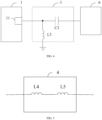
FIG. 2 is a schematic diagram showing a radio frequency path including a radio frequency cable according to Embodiment one. -
FIG. 3 is a schematic diagram showing a first capacitance limitation module according to Embodiment one. -
FIG. 4 is a schematic diagram showing a second capacitance limitation module according to Embodiment one. -
FIG. 5 is a schematic diagram showing a signal isolation module according to Embodiment one. -
FIG. 6 is a flow chart showing a method for reducing SAR according to Embodiment two. -
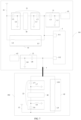
FIG. 7 is a schematic diagram showing an apparatus for reducing SAR on a mobile terminal according to Embodiment one. -
- 1-SAR sensor;
- 2-first capacitance limitation module;
- 3-second capacitance limitation module;
- 4-signal isolation module;
- 5-antenna;
- 6-power control circuit;
- 7-radio frequency cable;
- 8-antenna matching circuit;
- 11-detection port of the SAR sensor;
- 21-first capacitance limitation module for a first antenna;
- 22-first capacitance limitation module for a second antenna;
- 31-second capacitance limitation module for the first antenna;
- 32-second capacitance limitation module for the second antenna;
- 41-signal isolation module for the first antenna;
- 42-signal isolation module for the second antenna;
- 51-first antenna;
- 52-second antenna;
- 61-first power control circuit;
- 62-second power control circuit;
- 81-first antenna matching circuit;
- 82-second antenna matching circuit;
- 101-first circuit board;
- 102-second circuit board;
- 111-first detection port of the SAR sensor;
- 112-second detection port of the SAR sensor.
- Embodiments of the present disclosure are described with reference to the drawings as follows.
- In the present disclosure, a plurality of embodiments are described for illustrating rather than limiting. There may be more embodiments and solutions within a scope of the embodiments described in the present disclosure. Although some possible combinations of characteristics are shown in the drawings and discussed in the embodiments, other combinations of the characteristics disclosed herein may also be possible. Except for a case where limitation is specified, any characteristic or element of any embodiment may be combined with or replaced with any other characteristic or element in any other embodiment.
- The embodiments, characteristics and elements disclosed in the present disclosure may be combined with conventional characteristics or elements to form the solutions of the present disclosure. Any characteristic or element of any of the embodiments may be combined with a characteristic or element in another technical solution. Any feature shown and/or discussed in the present disclosure may be implemented individually or in any appropriate combination.
- SAR sensors emerge for protection of human health. An SAR sensor may automatically detect whether there is a human body approaching an antenna within a certain range of distances from the antenna. A human body is a semi-conductor. When the human body is approaching an antenna (metal), a capacitance value sensed by the antenna changes. A chip of the SAR sensor detects the closeness of the human body to the antenna by detecting capacitance changes of the antenna.
- As shown in
FIG. 1 , an embodiment of the present disclosure provides a device for detecting a specific absorption rate SAR, including: aSAR sensor 1, a plurality of firstcapacitance limitation modules 2, a plurality of secondcapacitance limitation modules 3, and a plurality ofsignal isolation modules 4. Herein, theSAR sensor 1 includes a plurality ofdetection ports 11, and each of thedetection port 11 is configured to perform SAR detection on one of theantennas 5. A first end of each of the firstcapacitance limitation module 2 is connected to one of theantennas 5; a second end of the firstcapacitance limitation module 2 is connected to one of thedetection ports 11. The firstcapacitance limitation module 2 is configured to limit a capacitance value on anantenna 5 side. A first end of a secondcapacitance limitation modules 3 is connected to one of thedetection ports 11, a second end of the secondcapacitance limitation module 3 is connected to apower control circuit 6, and the secondcapacitance limitation module 3 is configured to limit a capacitance value on apower control circuit 6 side. A first end of each of thesignal isolation modules 4 is connected to one of theantennas 5, a second end of thesignal isolation modules 4 is connected to one of thedetection ports 11, and thesignal isolation module 4 is configured to isolate radio frequency signals on a radio frequency path between theantenna 5 and thepower control circuit 6 and to transmit SAR signals of theantenna 5. - In one implementation, as shown in
FIG. 2 , in a case where theantenna 5 and theSAR sensor 1 are not on a same circuit board, the radio frequency path between theantenna 5 and thepower control circuit 6 includes aradio frequency cable 7 connecting two circuit boards. A first end of theradio frequency cable 7 is configured to be separately connected to a second end of a firstcapacitance limitation module 2 and a second end of asignal isolation module 4, and a second end of theradio frequency cable 7 is configured to be connected to thedetection port 11. Herein, theSAR sensor 1 and thepower control circuit 6 are provided on afirst circuit board 101, and theantenna 5 is provided on asecond circuit board 102. - In one implementation, the
first circuit board 101 is a main board, while thesecond circuit board 102 is a sub-board; or thefirst circuit board 101 is the sub-board, while thesecond circuit board 102 is the main board. - In the above implementation, SAR detection of an antenna not on the same circuit board as the SAR sensor may be performed by using a radio frequency cable between two circuit boards. In this way, one SAR sensor chip may synchronously perform SAR detection on multiple antennas.
- In one implementation, the radio frequency path between the
antenna 5 and thepower control circuit 6 includes anantenna matching circuit 8, theantenna matching circuit 8 includes a resistor, a capacitor and an inducer, and is configured to perform impedance matching on theantenna 5. There may be various forms of theantenna matching circuit 8, and the circuit is well known in the art. - As shown in
FIG. 3 , the radio frequency path between theantenna 5 and thepower control circuit 6 includes theantenna matching circuit 8 configured to perform impedance matching on theantenna 5. - The first
capacitance limitation module 2 includes: a first capacitor C1, a second capacitor C2, a first inducer L1 and a second inducer L2; a first end of the first capacitor C1 is taken as a first end of the firstcapacitance limitation module 2, a second end of the first capacitor C1 is connected to a first end of the first inducer L1 and a first end of theantenna matching circuit 8 respectively, and a second end of the first inducer L1 is grounded; a first end of the second capacitor C2 is separately connected to a second end of theantenna matching circuit 8 and a first end of the second inducer L2, and a second end of the second inducer L2 is grounded; and a second end of the second capacitor C2 is taken as a second end of the firstcapacitance limitation module 2. - In one implementation, as shown in
FIG. 4 , a secondcapacitance limitation module 3 includes a third capacitor C3 and a third inducer L3; a first end of the third capacitor C3 is taken as a first end of the secondcapacitance limitation module 3, a second end of the third capacitor C3 is taken as a second end of the secondcapacitance limitation module 3; and a first end of the third inducer L3 is connected to the first end of the third capacitor C3, and a second end of the third inducer L3 is grounded. Herein, the firstcapacitance limitation module 2 may make a capacitance value detected at anantenna 5 side by thedetection port 11 of the SAR sensor not change with capacitance of theantenna matching circuit 8, thereby a big capacitance of theantenna matching circuit 8 will not affect thedetection port 11 of the SAR sensor. - The second
capacitance limitation module 3 may make a capacitance value detected at apower control circuit 6 side by thedetection port 11 of the SAR sensor not change with capacitance of thepower control circuit 6, thereby a big capacitance of thepower control circuit 6 will not affect thedetection port 11 of the SAR sensor. - In one implementation, as shown in
FIG. 5 , thesignal isolation module 4 includes an inducer L4 and an inducer L5; and a first end of the inducer L4 is taken as a first end of thesignal isolation module 4, a second end of the inducer L4 is connected to a first end of the inducer L5, and a second end of the inducer L5 is taken as a second end of thesignal isolation module 4. Herein, frequency of the SAR detecting signals is low, for example, from dozens to hundreds of KHzs. However, frequency of communication signals on a radio frequency path between an antenna and an antenna signal transceiver module is usually as much as hundreds of MHz to several GHz, and power thereof is large. By setting thesignal isolation module 4 before thedetection port 11 of the SAR sensor, high-frequency communication signals on the antenna may be prevented from affecting SAR detection through blocking of inductance on the high-frequency communication signals, and SAR signals on theantenna 5 may be transmitted. - Compared with existing technologies, the device for detecting SAR according to the embodiment of the present disclosure uses multiple channels of an SAR sensor to perform SAR detection on multiple antennas, and uses a signal isolation module so that the radio frequency signals between an antenna and a power control circuit will not affect a detection port of the SAR sensor and a big capacitance will not affect the SAR detection.
- As shown in
FIG. 6 , an embodiment of the present disclosure provides a method for reducing a specific absorption rate SAR, including following steps: at step S110: SAR signals of a plurality of antennas are obtained respectively through a plurality of detection channels of an SAR sensor; at step S120: closeness of a human body to an antenna corresponding to the each detection channel is determined according to an SAR signal obtained through each detection channel; and at step S130: a transmission power of an antenna is reduced if the closeness of the human body to the antenna is less than or equal to a safe distance. - In the above implementations, a mobile terminal may be held by a user with various gestures. In some scenarios, one antenna in the mobile terminal may be close to the user so that the SAR is excessively high, while other antennas are distant from the user and SARs of these antennas are not excessively high. With one SAR sensor synchronously detecting SAR signals of multiple antennas and then processing SAR signals of each antenna respectively, reducing SARs of each antenna may be independently. Therefore, the solution for reducing SAR is more flexible and hardware cost thereof is reduced.
- An embodiment of the present disclosure provides a mobile terminal including the device for detecting SAR according to Embodiment one.
- The technical solution of detecting SAR in the present disclosure is described with the following examples.
- As shown in
FIG. 7 , this example provides a device for detecting SAR in a mobile terminal. The mobile terminal includes: a first circuit board (main board) 101; a second circuit board (sub-board) 102; a first antenna (WiFi antenna) 51, a firstpower control circuit 61, a secondpower control circuit 62 and a device for detecting SAR, provided on themain board 101; and a second antenna (main antenna) 52 provided on the sub-board 102. - The device for detecting SAR includes an
SAR sensor 1, a firstcapacitance limitation module 21 for the first antenna, a secondcapacitance limitation module 31 for the first antenna, asignal isolation module 41 for the first antenna, a first capacitance limitation module 22 for the second antenna, a secondcapacitance limitation module 32 for the second antenna and asignal isolation module 42 for the second antenna. - The
SAR sensor 1 includes afirst detection port 111 and asecond detection port 112. Thefirst detection port 111 is configured to perform SAR detection on thefirst antenna 51, and thesecond detection port 112 is configured to perform SAR detection on thesecond antenna 52. - A radio frequency path between the
first antenna 51 and the firstpower control circuit 61 includes a firstantenna matching circuit 81. A radio frequency path between thesecond antenna 52 and the secondpower control circuit 62 includes a secondantenna matching circuit 82. Each of the firstantenna matching circuit 81 and the secondantenna matching circuit 82 includes a resistor, a capacitor and an inducer and is configured to perform impedance matching on the antenna. There may be various forms of the circuits which is commonly known in the art. - The first
capacitance limitation module 21 for the first antenna includes a first capacitor C1, a second capacitor C2, a first inducer L1 and a second inducer L2. A first end of the first capacitor C1 is taken as a first end of the firstcapacitance limitation module 21 for the first antenna and is connected to thefirst antenna 51. A second end of the first capacitor C1 is connected to a first end of the first inducer L1 and a first end of the firstantenna matching circuit 81 respectively. A second end of the first inducer L1 is grounded. A first end of the second capacitor C2 is connected to a second end of the firstantenna matching circuit 81 and a first end of the second inducer L2 respectively. A second end of the second inducer L2 is grounded. A second end of the second capacitor C2 is taken as a second end of the firstcapacitance limitation module 21 for the first antenna and is connected to thefirst detection port 111. - The second
capacitance limitation module 31 for the first antenna includes a third capacitor C3 and a third inducer L3. A first end of the third capacitor C3 is taken as a first end of the secondcapacitance limitation module 31 for the first antenna and is connected to thefirst detection port 111. A second end of the third capacitor C3 is taken as a second end of the secondcapacitance limitation module 31 for the first antenna and is connected to the firstpower control circuit 61. A first end of the third inducer L3 is connected to the first end of the third capacitor C3, and a second end of the third inducer L3 is grounded. - The
signal isolation module 41 for the first antenna includes an inducer L4 and an inducer L5. A first end of the inducer L4 is taken as a first end of thesignal isolation module 41 for the first antenna and is connected to thefirst antenna 51. A second end of the inducer L4 is connected to a first end of the inducer L5. A second end of the inducer L5 is taken as a second end of thesignal isolation module 41 for the first antenna and is connected to thefirst detection port 111. Thesignal isolation module 41 for the first antenna is configured to isolate radio frequency signals on the radio frequency path between thefirst antenna 51 and the firstpower control circuit 61, and to transmit SAR signals of thefirst antenna 51. - The
second antenna 52 is provided on the sub-board 102. Both theSAR sensor 1 and the secondpower control circuit 62 are provided on themain board 101. Therefore, the radio frequency path between thesecond antenna 52 and the secondpower control circuit 62 further includes aradio frequency cable 7 connecting across two circuit boards. A first end of theradio frequency cable 7 is configured to be connected to a second end of the first capacitance limitation module 22 for the second antenna and a second end of thesignal isolation module 42 for the second antenna respectively. The second end of theradio frequency cable 7 is configured to be connected to thesecond detection port 112. - The first capacitance limitation module 22 for the second antenna includes a capacitor C6, a capacitor C7, an inducer L6 and an inducer L7. A first end of the capacitor C6 is taken as a first end of the first capacitance limitation module 22 for the second antenna and is connected to the
second antenna 52. A second end of the capacitor C6 is respectively connected to a first end of the inducer L6 and a first end of the secondantenna matching circuit 82. A second end of the inducer L6 is grounded. A first end of the capacitor C7 is connected to a second end of the secondantenna matching circuit 82 and a first end of the inducer L7 respectively. A second end of the inducer L7 is grounded. A second end of the capacitor C7 is taken as a second end of the first capacitance limitation module 22 for the second antenna and is connected to the first end of theradio frequency cable 7. The second end of theradio frequency cable 7 is connected to thesecond detection port 112. - The second
capacitance limitation module 32 for the second antenna includes a capacitor C8 and an inducer L8. A first end of the capacitor C8 is taken as a first end of the secondcapacitance limitation module 32 for the second antenna and is connected to thesecond detection port 112. A second end of the capacitor C8 is taken as a second end of the secondcapacitance limitation module 32 for the second antenna and is connected to the secondpower control circuit 62. A first end of the inducer L8 is connected to the first end of the capacitor C8, and a second end of the inducer L8 is grounded. - The
signal isolation module 42 for the second antenna includes an inducer L9 and an inducer L10. A first end of the inducer L9 is taken as a first end of thesignal isolation module 42 for the second antenna and is connected to thesecond antenna 52. A second end of the inducer L9 is connected to a first end of the inducer L10. A second end of the inducer L10 is taken as a second end of thesignal isolation module 42 for the second antenna and is connected to the first end of theradio frequency cable 7. The second end of theradio frequency cable 7 is connected to thesecond detection port 112. Thesignal isolation module 42 for the second antenna is configured to isolate radio frequency signals on the radio frequency path between thesecond antenna 52 and the secondpower control circuit 62, and to transmit SAR signals of thesecond antenna 52. - The mobile terminal obtains SAR signals of the first antenna through the first detection channel of the SAR sensor, obtains SAR signals of the second antenna through the second detection channel of the SAR sensor, determines whether a distance between the human body and the first antenna is smaller than or equal to a safe threshold according to the SAR signals of the first antenna, and determines whether a distance between the human body and the second antenna is smaller than or equal to the safe threshold according to the SAR signals of the second antenna. When the distance between the human body and the first antenna is smaller than or equal to the safe threshold, the transmission power of the first antenna is reduced. When the distance between the human body and the second antenna is smaller than or equal to the safe threshold, the transmission power of the second antenna is reduced.
- In the above example, the mobile terminal transmits SAR signals of the antenna (main antenna) distant from the detection port of the SAR sensor through a radio frequency cable available between the main board and the sub-board. In this way, in a case where the cost of SAR devices or area for distribution of the devices is not increased, one SAR sensor chip may synchronously detect SAR signals of an antenna (WiFi antenna) close to the SAR sensor and SAR signals of an antenna (main antenna) far away from the SAR sensor. With one SAR sensor synchronously detecting SAR signals of two antennas, the mobile terminal separately processes SAR signals of each antenna, and control of reducing SARs of each antenna independently may be achieved. Therefore, a solution of reducing SAR is more flexible and hardware cost thereof is reduced.
Claims (5)
- A device for detecting specific absorption rate, SAR, comprising: a SAR sensor (1),a plurality of first capacitance limitation modules (2), a plurality of second capacitance limitation modules (3), and a plurality of signal isolation modules (4); characterised in that,the SAR sensor (1) comprises a plurality of detection ports (11), and each of the plurality of detection ports (11) is configured to perform SAR detection on one of a plurality of antennas (5);wherein the device for detecting specific absorption rate SAR is specified so that, a first end of each of the plurality of first capacitance limitation modules (2) is connected to a respective antenna (5) of the plurality of antennas (5), a second end of each of the plurality of first capacitance limitation modules (2) is connected to a respective detection port (11) of the plurality of detection ports (11), and each of the plurality of first capacitance limitation modules (2) is configured to limit a capacitance value on the respective antenna (5) side detected by the detection port (11), wherein each of the plurality of first capacitance limitation modules (2) comprises: a first capacitor C1, a second capacitor C2, a first inducer L1 and a second inducer L2;a first end of each of the plurality of second capacitance limitation modules (3) is connected to a respective detection port (11) of the plurality of detection ports (11), a second end of each of the plurality of second capacitance limitation modules (3) is connected to a respective power control circuit (6) of a plurality of power control circuits (6), and each of the plurality of second capacitance limitation modules (3) is configured to limit a capacitance value on the respective power control circuit (6) side detected by the detection port (11), wherein each of the plurality second capacitance limitation modules (3) comprises a third capacitor C3 and a third inducer L3; a first end of the third capacitor C3 is taken as a first end of the second capacitance limitation module (3), a second end of the third capacitor C3 is taken as a second end of the second capacitance limitation module (3); and a first end of the third inducer L3 is connected to the first end of the third capacitor C3, and a second end of the third inducer L3 is grounded;a first end of each of the plurality of signal isolation modules (4) is connected to a respective antenna (5) of the plurality of antennas (5), a second end of each of the plurality of signal isolation modules (4) is connected to a respective detection port (11) of the plurality of detection ports (11), and each of the plurality of signal isolation modules (4) is configured to isolate a radio frequency signal on a radio frequency path between the respective antenna (5) and the respective power control circuit (6) and to transmit a SAR signal of the respective antenna (5); andthe radio frequency path between the respective antenna (5) and the respective power control circuit (6) comprises an antenna matching circuit (8) configured to perform impedance matching on the respective antenna (5); a first end of the first capacitor C1 in each first capacitance limitation module is taken as the first end of the first capacitance limitation module (2), a second end of the first capacitor C1 is connected to a first end of the first inducer L1 and a first end of the antenna matching circuit (8) respectively, and a second end of the first inducer L1 is grounded; a first end of the second capacitor C2 is connected to a second end of the antenna matching circuit (8) and a first end of the second inducer L2 respectively, and a second end of the second inducer L2 is grounded; a second end of the second capacitor C2 is taken as a second end of the first capacitance limitation module (2); the second end of the first capacitor C1 is taken as a third end of the first capacitance limitation module (2); and the first end of the second capacitor C2 is taken as a forth end of the first capacitance limitation module (2).
- The device according to claim 1, wherein
in response to the SAR sensor (1) and the plurality of power control circuits (6) being on a first circuit board (101) and the plurality of antennas (5) being on a second circuit board (102) which is different from the first circuit board (101), the radio frequency path between the respective antenna (5) and the respective power control circuit (6) comprises a radio frequency cable (7) connecting across the first circuit board (101) and the second circuit board (102); a first end of the radio frequency cable (7) is configured to be connected to a second end of one of the plurality of first capacitance limitation modules (2) and a second end of one of the plurality of signal isolation modules (4), and a second end of the radio frequency cable (7) is configured to be connected to one of the plurality of detection ports (11). - The device according to claim 1, wherein
each of the plurality of signal isolation modules (4) comprises a fourth inducer L4 and a fifth inducer L5; and a first end of the fourth inducer L4 is taken as the first end of the signal isolation module (4), a second end of the fourth inducer L4 is connected to a first end of the fifth inducer L5, and a second end of the fifth inducer L5 is taken as a second end of the signal isolation module (4). - The device according to claim 2, wherein
the first circuit board (101) is a main board, and the second circuit board (102) is a sub-board; or the first circuit board (101) is the sub-board, and the second circuit board (102) is the main board. - A mobile terminal comprising the device for detecting the specific absorption rate SAR according to any one of claims 1-4.
Applications Claiming Priority (2)
| Application Number | Priority Date | Filing Date | Title |
|---|---|---|---|
| CN201910630690.1A CN112114202B (en) | 2019-07-12 | 2019-07-12 | Device for detecting SAR, method for reducing SAR, and mobile terminal |
| PCT/CN2020/093857 WO2021008261A1 (en) | 2019-07-12 | 2020-06-02 | Device for detecting sar, method for reducing sar, and mobile terminal |
Publications (3)
| Publication Number | Publication Date |
|---|---|
| EP3978939A1 EP3978939A1 (en) | 2022-04-06 |
| EP3978939A4 EP3978939A4 (en) | 2022-08-03 |
| EP3978939B1 true EP3978939B1 (en) | 2025-02-12 |
Family
ID=73795335
Family Applications (1)
| Application Number | Title | Priority Date | Filing Date |
|---|---|---|---|
| EP20840505.0A Active EP3978939B1 (en) | 2019-07-12 | 2020-06-02 | Device for detecting sar and mobile terminal |
Country Status (7)
| Country | Link |
|---|---|
| US (2) | US12320760B2 (en) |
| EP (1) | EP3978939B1 (en) |
| JP (1) | JP7319392B2 (en) |
| KR (1) | KR102656820B1 (en) |
| CN (1) | CN112114202B (en) |
| ES (1) | ES3021814T3 (en) |
| WO (1) | WO2021008261A1 (en) |
Families Citing this family (22)
| Publication number | Priority date | Publication date | Assignee | Title |
|---|---|---|---|---|
| CN111682324B (en) * | 2020-06-22 | 2022-01-21 | 华勤技术股份有限公司 | Circuit and method for reducing SAR of antenna |
| CN112768959B (en) * | 2020-12-29 | 2024-01-02 | Oppo广东移动通信有限公司 | Antenna assembly and electronic equipment |
| CN112751213B (en) * | 2020-12-29 | 2023-02-28 | Oppo广东移动通信有限公司 | Antenna assembly and electronic equipment |
| CN112751212B (en) | 2020-12-29 | 2023-08-04 | Oppo广东移动通信有限公司 | Antenna systems and electronics |
| CN112751174B (en) * | 2020-12-29 | 2024-01-02 | Oppo广东移动通信有限公司 | Antenna assembly and electronic equipment |
| CN112821031B (en) * | 2020-12-29 | 2024-01-02 | Oppo广东移动通信有限公司 | Electronic equipment |
| CN115036676B (en) * | 2021-03-03 | 2024-02-20 | Oppo广东移动通信有限公司 | Antenna assembly and electronic equipment |
| CN113068249B (en) * | 2021-03-09 | 2023-11-14 | 维沃移动通信有限公司 | Signal transmitting method, device, electronic equipment and readable storage medium |
| CN115342720A (en) | 2021-05-14 | 2022-11-15 | Oppo广东移动通信有限公司 | Electronic device |
| CN115343537B (en) * | 2021-05-14 | 2026-01-23 | Oppo广东移动通信有限公司 | SAR detection assembly, detection method and electronic equipment |
| CN115704919B (en) * | 2021-08-03 | 2026-03-10 | 南京矽力微电子(香港)有限公司 | Mobile device |
| CN115808574A (en) * | 2021-09-14 | 2023-03-17 | 北京小米移动软件有限公司 | Antenna module and terminal equipment |
| CN215499825U (en) * | 2021-09-18 | 2022-01-11 | Oppo广东移动通信有限公司 | Electronic device |
| CN114189926B (en) * | 2021-11-10 | 2025-04-22 | 联想(北京)有限公司 | Antenna working power adjustment method, device, equipment and readable storage medium |
| CN116359619A (en) * | 2021-12-28 | 2023-06-30 | 北京小米移动软件有限公司 | Electronic equipment |
| CN114755501A (en) * | 2022-04-18 | 2022-07-15 | 华勤技术股份有限公司 | SAR detection device and electronic equipment |
| CN114899597B (en) * | 2022-05-07 | 2025-12-09 | 维沃移动通信有限公司 | Electronic equipment |
| CN114924134B (en) * | 2022-05-30 | 2023-12-19 | Oppo广东移动通信有限公司 | Electronic equipment |
| KR20230175068A (en) | 2022-06-22 | 2023-12-29 | 삼성전자주식회사 | Electronic device including multi channel grip sensor and method for sensing of change of capacitance using the multi channel grip sensor |
| CN115277911A (en) * | 2022-07-06 | 2022-11-01 | 上海龙旗科技股份有限公司 | Method and device for acquiring specific absorption rate SAR of mobile phone |
| US20250030150A1 (en) * | 2022-09-08 | 2025-01-23 | Kunshan Innowave Communication Technology Co., Ltd. | Antenna for mobile terminal, and mobile terminal |
| CN116169460A (en) * | 2023-03-06 | 2023-05-26 | 华勤技术股份有限公司 | Antenna system, method, terminal and storage medium for reducing SAR value |
Family Cites Families (23)
| Publication number | Priority date | Publication date | Assignee | Title |
|---|---|---|---|---|
| US6362789B1 (en) * | 2000-12-22 | 2002-03-26 | Rangestar Wireless, Inc. | Dual band wideband adjustable antenna assembly |
| WO2012108254A1 (en) * | 2011-02-09 | 2012-08-16 | 株式会社村田製作所 | High-frequency module |
| US9026059B2 (en) * | 2011-02-17 | 2015-05-05 | Futurewei Technologies, Inc. | Adaptive maximum power limiting using capacitive sensing in a wireless device |
| DE102011004622B4 (en) | 2011-02-23 | 2013-04-18 | Ident Technology Ag | Capacitive sensor device and radio device with capacitive sensor device and method for setting a transmission power of a radio device |
| US8326385B2 (en) * | 2011-04-05 | 2012-12-04 | Research In Motion Limited | Mobile wireless communications device with proximity based transmitted power control and related methods |
| CN103428314A (en) * | 2012-05-24 | 2013-12-04 | 中兴通讯股份有限公司 | Method for adjusting radiation direction of mobile terminal, and mobile terminal |
| JP2014082735A (en) | 2012-09-26 | 2014-05-08 | Panasonic Corp | Communication apparatus and electronic apparatus |
| CN103067038B (en) * | 2013-01-05 | 2017-08-18 | 中兴通讯股份有限公司 | A kind of mobile terminal and the method for reducing specific absorption rate |
| JP6268612B2 (en) * | 2013-02-21 | 2018-01-31 | パナソニックIpマネジメント株式会社 | Electronics |
| CN104779435A (en) * | 2015-04-29 | 2015-07-15 | 联想(北京)有限公司 | Induction device and electronic device |
| US9490885B1 (en) * | 2015-05-01 | 2016-11-08 | Amazon Technologies, Inc. | Proximity sensor and antenna system arrangement for metal housing |
| CN106550067B (en) * | 2015-09-22 | 2019-04-19 | 葫芦科技有限公司 | A kind of method that mobile communication terminal reduces SAR |
| US10673477B2 (en) * | 2015-10-21 | 2020-06-02 | Tendyron Corporation | Communication device, adapter device, communication system |
| CN106207375B (en) * | 2016-06-30 | 2019-08-27 | 联想(北京)有限公司 | A kind of electronic equipment |
| CN206098681U (en) * | 2016-10-19 | 2017-04-12 | 深圳市信维通信股份有限公司 | System for reduce high frequency cell -phone antenna SAR value |
| US10461406B2 (en) * | 2017-01-23 | 2019-10-29 | Microsoft Technology Licensing, Llc | Loop antenna with integrated proximity sensing |
| CN107548145A (en) | 2017-06-27 | 2018-01-05 | 西安易朴通讯技术有限公司 | Antenna assembly, mobile terminal and antenna adjustment method |
| CN108075795B (en) * | 2017-12-26 | 2023-11-28 | 深圳市强军科技有限公司 | Radio frequency front-end device of multi-frequency receiver |
| US10367260B1 (en) * | 2018-01-09 | 2019-07-30 | Motorola Mobility Llc | Dynamic reduction of current drain for antenna tuner of a communication device |
| US10321463B1 (en) * | 2018-01-16 | 2019-06-11 | Dell Products, Lp | Method and apparatus for an accelerometer assisted control system for a reconfigurable antenna communication device |
| CN109088151B (en) * | 2018-07-04 | 2021-04-20 | 深圳市万普拉斯科技有限公司 | Antenna system and mobile terminal |
| CN109474740A (en) * | 2018-11-08 | 2019-03-15 | 闻泰通讯股份有限公司 | Reduce method, system and the mobile terminal of SAR value |
| CN209170386U (en) * | 2018-11-21 | 2019-07-26 | 维沃移动通信有限公司 | Radio frequency assembly, conduction testing equipment and terminal |
-
2019
- 2019-07-12 CN CN201910630690.1A patent/CN112114202B/en active Active
-
2020
- 2020-06-02 JP JP2021569164A patent/JP7319392B2/en active Active
- 2020-06-02 WO PCT/CN2020/093857 patent/WO2021008261A1/en not_active Ceased
- 2020-06-02 KR KR1020217038278A patent/KR102656820B1/en active Active
- 2020-06-02 US US17/624,230 patent/US12320760B2/en active Active
- 2020-06-02 EP EP20840505.0A patent/EP3978939B1/en active Active
- 2020-06-02 ES ES20840505T patent/ES3021814T3/en active Active
-
2025
- 2025-05-01 US US19/196,589 patent/US20250258110A1/en active Pending
Also Published As
| Publication number | Publication date |
|---|---|
| ES3021814T3 (en) | 2025-05-27 |
| WO2021008261A1 (en) | 2021-01-21 |
| KR102656820B1 (en) | 2024-04-11 |
| JP7319392B2 (en) | 2023-08-01 |
| KR20220005038A (en) | 2022-01-12 |
| CN112114202A (en) | 2020-12-22 |
| US20220349839A1 (en) | 2022-11-03 |
| CN112114202B (en) | 2021-07-23 |
| EP3978939A4 (en) | 2022-08-03 |
| US20250258110A1 (en) | 2025-08-14 |
| EP3978939A1 (en) | 2022-04-06 |
| JP2022539949A (en) | 2022-09-14 |
| US12320760B2 (en) | 2025-06-03 |
Similar Documents
| Publication | Publication Date | Title |
|---|---|---|
| US20250258110A1 (en) | Device for detecting sar, method for reducing sar, and mobile terminal | |
| EP4220974A1 (en) | Radio frequency l-pa mid device, radio frequency transceiving system, and communication equipment | |
| EP4152624B1 (en) | Radio-frequency pa mid device, radio-frequency system and communication device | |
| CN109121443B (en) | Closed loop aperture adjustable antenna | |
| CN105871407B (en) | A kind of electronic equipment | |
| US9577332B2 (en) | Electronic device and multi-band antenna | |
| EP4142164B1 (en) | Radio frequency pa mid device, radio frequency transceiving system, and communication device | |
| CN106207375B (en) | A kind of electronic equipment | |
| CN108055410A (en) | Antenna switching circuit, antenna switching method and electronic device | |
| CN112736459B (en) | Dual antenna systems, RF architecture and electronics | |
| EP3571768A1 (en) | Loop antenna with integrated proximity sensing | |
| US9800354B2 (en) | Wireless communication apparatus | |
| CN110829023B (en) | Antenna modules and terminals | |
| CN208128362U (en) | Antenna switching circuit and electronic device | |
| US9748994B2 (en) | Communication module | |
| CN111697985A (en) | 5G radio frequency receiving circuit and wireless communication equipment | |
| US20160172749A1 (en) | Hybrid antenna and integrated proximity sensor using a shared conductive structure | |
| US20160211881A1 (en) | Wireless communication device capable of adjusting at least one antenna to improve efficiency of other coexisting antenna(s) and related wireless communication method | |
| US20200321990A1 (en) | Antenna Switching Circuit, Antenna Switching Method and Electronic Device | |
| US20180375206A1 (en) | Electric composite detection antenna | |
| US12395196B2 (en) | Radio-frequency L-DRX device, radio-frequency transceiving system, and communication apparatus | |
| EP2738947A1 (en) | Radio frequency switch | |
| JP2016178481A (en) | Communication module and communication control method |
Legal Events
| Date | Code | Title | Description |
|---|---|---|---|
| STAA | Information on the status of an ep patent application or granted ep patent |
Free format text: STATUS: THE INTERNATIONAL PUBLICATION HAS BEEN MADE |
|
| PUAI | Public reference made under article 153(3) epc to a published international application that has entered the european phase |
Free format text: ORIGINAL CODE: 0009012 |
|
| STAA | Information on the status of an ep patent application or granted ep patent |
Free format text: STATUS: REQUEST FOR EXAMINATION WAS MADE |
|
| 17P | Request for examination filed |
Effective date: 20211229 |
|
| AK | Designated contracting states |
Kind code of ref document: A1 Designated state(s): AL AT BE BG CH CY CZ DE DK EE ES FI FR GB GR HR HU IE IS IT LI LT LU LV MC MK MT NL NO PL PT RO RS SE SI SK SM TR |
|
| A4 | Supplementary search report drawn up and despatched |
Effective date: 20220630 |
|
| RIC1 | Information provided on ipc code assigned before grant |
Ipc: H04W 52/28 20090101ALI20220624BHEP Ipc: G01R 29/08 20060101ALI20220624BHEP Ipc: G01R 29/10 20060101AFI20220624BHEP |
|
| DAV | Request for validation of the european patent (deleted) | ||
| DAX | Request for extension of the european patent (deleted) | ||
| STAA | Information on the status of an ep patent application or granted ep patent |
Free format text: STATUS: EXAMINATION IS IN PROGRESS |
|
| 17Q | First examination report despatched |
Effective date: 20230731 |
|
| GRAP | Despatch of communication of intention to grant a patent |
Free format text: ORIGINAL CODE: EPIDOSNIGR1 |
|
| STAA | Information on the status of an ep patent application or granted ep patent |
Free format text: STATUS: GRANT OF PATENT IS INTENDED |
|
| INTG | Intention to grant announced |
Effective date: 20241121 |
|
| GRAS | Grant fee paid |
Free format text: ORIGINAL CODE: EPIDOSNIGR3 |
|
| GRAA | (expected) grant |
Free format text: ORIGINAL CODE: 0009210 |
|
| STAA | Information on the status of an ep patent application or granted ep patent |
Free format text: STATUS: THE PATENT HAS BEEN GRANTED |
|
| AK | Designated contracting states |
Kind code of ref document: B1 Designated state(s): AL AT BE BG CH CY CZ DE DK EE ES FI FR GB GR HR HU IE IS IT LI LT LU LV MC MK MT NL NO PL PT RO RS SE SI SK SM TR |
|
| REG | Reference to a national code |
Ref country code: GB Ref legal event code: FG4D |
|
| REG | Reference to a national code |
Ref country code: CH Ref legal event code: EP |
|
| REG | Reference to a national code |
Ref country code: DE Ref legal event code: R096 Ref document number: 602020046061 Country of ref document: DE |
|
| REG | Reference to a national code |
Ref country code: IE Ref legal event code: FG4D |
|
| REG | Reference to a national code |
Ref country code: ES Ref legal event code: FG2A Ref document number: 3021814 Country of ref document: ES Kind code of ref document: T3 Effective date: 20250527 |
|
| REG | Reference to a national code |
Ref country code: NL Ref legal event code: MP Effective date: 20250212 |
|
| PG25 | Lapsed in a contracting state [announced via postgrant information from national office to epo] |
Ref country code: RS Free format text: LAPSE BECAUSE OF FAILURE TO SUBMIT A TRANSLATION OF THE DESCRIPTION OR TO PAY THE FEE WITHIN THE PRESCRIBED TIME-LIMIT Effective date: 20250512 |
|
| PG25 | Lapsed in a contracting state [announced via postgrant information from national office to epo] |
Ref country code: FI Free format text: LAPSE BECAUSE OF FAILURE TO SUBMIT A TRANSLATION OF THE DESCRIPTION OR TO PAY THE FEE WITHIN THE PRESCRIBED TIME-LIMIT Effective date: 20250212 |
|
| PG25 | Lapsed in a contracting state [announced via postgrant information from national office to epo] |
Ref country code: PL Free format text: LAPSE BECAUSE OF FAILURE TO SUBMIT A TRANSLATION OF THE DESCRIPTION OR TO PAY THE FEE WITHIN THE PRESCRIBED TIME-LIMIT Effective date: 20250212 |
|
| PGFP | Annual fee paid to national office [announced via postgrant information from national office to epo] |
Ref country code: DE Payment date: 20250618 Year of fee payment: 6 |
|
| REG | Reference to a national code |
Ref country code: LT Ref legal event code: MG9D |
|
| PG25 | Lapsed in a contracting state [announced via postgrant information from national office to epo] |
Ref country code: IS Free format text: LAPSE BECAUSE OF FAILURE TO SUBMIT A TRANSLATION OF THE DESCRIPTION OR TO PAY THE FEE WITHIN THE PRESCRIBED TIME-LIMIT Effective date: 20250612 Ref country code: NO Free format text: LAPSE BECAUSE OF FAILURE TO SUBMIT A TRANSLATION OF THE DESCRIPTION OR TO PAY THE FEE WITHIN THE PRESCRIBED TIME-LIMIT Effective date: 20250512 |
|
| PG25 | Lapsed in a contracting state [announced via postgrant information from national office to epo] |
Ref country code: NL Free format text: LAPSE BECAUSE OF FAILURE TO SUBMIT A TRANSLATION OF THE DESCRIPTION OR TO PAY THE FEE WITHIN THE PRESCRIBED TIME-LIMIT Effective date: 20250212 |
|
| PG25 | Lapsed in a contracting state [announced via postgrant information from national office to epo] |
Ref country code: HR Free format text: LAPSE BECAUSE OF FAILURE TO SUBMIT A TRANSLATION OF THE DESCRIPTION OR TO PAY THE FEE WITHIN THE PRESCRIBED TIME-LIMIT Effective date: 20250212 |
|
| PG25 | Lapsed in a contracting state [announced via postgrant information from national office to epo] |
Ref country code: PT Free format text: LAPSE BECAUSE OF FAILURE TO SUBMIT A TRANSLATION OF THE DESCRIPTION OR TO PAY THE FEE WITHIN THE PRESCRIBED TIME-LIMIT Effective date: 20250612 Ref country code: LV Free format text: LAPSE BECAUSE OF FAILURE TO SUBMIT A TRANSLATION OF THE DESCRIPTION OR TO PAY THE FEE WITHIN THE PRESCRIBED TIME-LIMIT Effective date: 20250212 |
|
| PG25 | Lapsed in a contracting state [announced via postgrant information from national office to epo] |
Ref country code: GR Free format text: LAPSE BECAUSE OF FAILURE TO SUBMIT A TRANSLATION OF THE DESCRIPTION OR TO PAY THE FEE WITHIN THE PRESCRIBED TIME-LIMIT Effective date: 20250513 Ref country code: BG Free format text: LAPSE BECAUSE OF FAILURE TO SUBMIT A TRANSLATION OF THE DESCRIPTION OR TO PAY THE FEE WITHIN THE PRESCRIBED TIME-LIMIT Effective date: 20250212 |
|
| REG | Reference to a national code |
Ref country code: AT Ref legal event code: MK05 Ref document number: 1766501 Country of ref document: AT Kind code of ref document: T Effective date: 20250212 |
|
| PG25 | Lapsed in a contracting state [announced via postgrant information from national office to epo] |
Ref country code: SE Free format text: LAPSE BECAUSE OF FAILURE TO SUBMIT A TRANSLATION OF THE DESCRIPTION OR TO PAY THE FEE WITHIN THE PRESCRIBED TIME-LIMIT Effective date: 20250212 |
|
| PG25 | Lapsed in a contracting state [announced via postgrant information from national office to epo] |
Ref country code: SM Free format text: LAPSE BECAUSE OF FAILURE TO SUBMIT A TRANSLATION OF THE DESCRIPTION OR TO PAY THE FEE WITHIN THE PRESCRIBED TIME-LIMIT Effective date: 20250212 |
|
| PGFP | Annual fee paid to national office [announced via postgrant information from national office to epo] |
Ref country code: ES Payment date: 20250731 Year of fee payment: 6 |
|
| PG25 | Lapsed in a contracting state [announced via postgrant information from national office to epo] |
Ref country code: DK Free format text: LAPSE BECAUSE OF FAILURE TO SUBMIT A TRANSLATION OF THE DESCRIPTION OR TO PAY THE FEE WITHIN THE PRESCRIBED TIME-LIMIT Effective date: 20250212 |
|
| PGFP | Annual fee paid to national office [announced via postgrant information from national office to epo] |
Ref country code: IT Payment date: 20250624 Year of fee payment: 6 |
|
| PG25 | Lapsed in a contracting state [announced via postgrant information from national office to epo] |
Ref country code: AT Free format text: LAPSE BECAUSE OF FAILURE TO SUBMIT A TRANSLATION OF THE DESCRIPTION OR TO PAY THE FEE WITHIN THE PRESCRIBED TIME-LIMIT Effective date: 20250212 |
|
| PG25 | Lapsed in a contracting state [announced via postgrant information from national office to epo] |
Ref country code: CZ Free format text: LAPSE BECAUSE OF FAILURE TO SUBMIT A TRANSLATION OF THE DESCRIPTION OR TO PAY THE FEE WITHIN THE PRESCRIBED TIME-LIMIT Effective date: 20250212 Ref country code: EE Free format text: LAPSE BECAUSE OF FAILURE TO SUBMIT A TRANSLATION OF THE DESCRIPTION OR TO PAY THE FEE WITHIN THE PRESCRIBED TIME-LIMIT Effective date: 20250212 |
|
| PG25 | Lapsed in a contracting state [announced via postgrant information from national office to epo] |
Ref country code: RO Free format text: LAPSE BECAUSE OF FAILURE TO SUBMIT A TRANSLATION OF THE DESCRIPTION OR TO PAY THE FEE WITHIN THE PRESCRIBED TIME-LIMIT Effective date: 20250212 |
|
| PG25 | Lapsed in a contracting state [announced via postgrant information from national office to epo] |
Ref country code: SK Free format text: LAPSE BECAUSE OF FAILURE TO SUBMIT A TRANSLATION OF THE DESCRIPTION OR TO PAY THE FEE WITHIN THE PRESCRIBED TIME-LIMIT Effective date: 20250212 |
|
| REG | Reference to a national code |
Ref country code: DE Ref legal event code: R097 Ref document number: 602020046061 Country of ref document: DE |
|
| PLBE | No opposition filed within time limit |
Free format text: ORIGINAL CODE: 0009261 |
|
| STAA | Information on the status of an ep patent application or granted ep patent |
Free format text: STATUS: NO OPPOSITION FILED WITHIN TIME LIMIT |
|
| REG | Reference to a national code |
Ref country code: CH Ref legal event code: L10 Free format text: ST27 STATUS EVENT CODE: U-0-0-L10-L00 (AS PROVIDED BY THE NATIONAL OFFICE) Effective date: 20251224 |
|
| 26N | No opposition filed |
Effective date: 20251113 |
|
| REG | Reference to a national code |
Ref country code: CH Ref legal event code: H13 Free format text: ST27 STATUS EVENT CODE: U-0-0-H10-H13 (AS PROVIDED BY THE NATIONAL OFFICE) Effective date: 20260127 |
|
| PG25 | Lapsed in a contracting state [announced via postgrant information from national office to epo] |
Ref country code: MC Free format text: LAPSE BECAUSE OF FAILURE TO SUBMIT A TRANSLATION OF THE DESCRIPTION OR TO PAY THE FEE WITHIN THE PRESCRIBED TIME-LIMIT Effective date: 20250212 |
|
| PG25 | Lapsed in a contracting state [announced via postgrant information from national office to epo] |
Ref country code: LU Free format text: LAPSE BECAUSE OF NON-PAYMENT OF DUE FEES Effective date: 20250602 |
|
| GBPC | Gb: european patent ceased through non-payment of renewal fee |
Effective date: 20250602 |
|
| REG | Reference to a national code |
Ref country code: BE Ref legal event code: MM Effective date: 20250630 |
|
| PG25 | Lapsed in a contracting state [announced via postgrant information from national office to epo] |
Ref country code: GB Free format text: LAPSE BECAUSE OF NON-PAYMENT OF DUE FEES Effective date: 20250602 |
|
| PG25 | Lapsed in a contracting state [announced via postgrant information from national office to epo] |
Ref country code: IE Free format text: LAPSE BECAUSE OF NON-PAYMENT OF DUE FEES Effective date: 20250602 |
|
| PG25 | Lapsed in a contracting state [announced via postgrant information from national office to epo] |
Ref country code: BE Free format text: LAPSE BECAUSE OF NON-PAYMENT OF DUE FEES Effective date: 20250630 |
|
| PG25 | Lapsed in a contracting state [announced via postgrant information from national office to epo] |
Ref country code: FR Free format text: LAPSE BECAUSE OF NON-PAYMENT OF DUE FEES Effective date: 20250630 |
|
| PG25 | Lapsed in a contracting state [announced via postgrant information from national office to epo] |
Ref country code: CH Free format text: LAPSE BECAUSE OF NON-PAYMENT OF DUE FEES Effective date: 20250630 |