EP3975252A1 - Semiconductor structure and manufacturing method for semiconductor structure - Google Patents
Semiconductor structure and manufacturing method for semiconductor structure Download PDFInfo
- Publication number
- EP3975252A1 EP3975252A1 EP21783384.7A EP21783384A EP3975252A1 EP 3975252 A1 EP3975252 A1 EP 3975252A1 EP 21783384 A EP21783384 A EP 21783384A EP 3975252 A1 EP3975252 A1 EP 3975252A1
- Authority
- EP
- European Patent Office
- Prior art keywords
- layer
- trench
- semiconductor structure
- groove
- type
- Prior art date
- Legal status (The legal status is an assumption and is not a legal conclusion. Google has not performed a legal analysis and makes no representation as to the accuracy of the status listed.)
- Granted
Links
Images



Classifications
-
- H—ELECTRICITY
- H10—SEMICONDUCTOR DEVICES; ELECTRIC SOLID-STATE DEVICES NOT OTHERWISE PROVIDED FOR
- H10B—ELECTRONIC MEMORY DEVICES
- H10B12/00—Dynamic random access memory [DRAM] devices
- H10B12/30—DRAM devices comprising one-transistor - one-capacitor [1T-1C] memory cells
- H10B12/34—DRAM devices comprising one-transistor - one-capacitor [1T-1C] memory cells the transistor being at least partially in a trench in the substrate
-
- H—ELECTRICITY
- H10—SEMICONDUCTOR DEVICES; ELECTRIC SOLID-STATE DEVICES NOT OTHERWISE PROVIDED FOR
- H10B—ELECTRONIC MEMORY DEVICES
- H10B12/00—Dynamic random access memory [DRAM] devices
- H10B12/01—Manufacture or treatment
- H10B12/02—Manufacture or treatment for one transistor one-capacitor [1T-1C] memory cells
- H10B12/05—Making the transistor
- H10B12/053—Making the transistor the transistor being at least partially in a trench in the substrate
-
- H—ELECTRICITY
- H10—SEMICONDUCTOR DEVICES; ELECTRIC SOLID-STATE DEVICES NOT OTHERWISE PROVIDED FOR
- H10B—ELECTRONIC MEMORY DEVICES
- H10B12/00—Dynamic random access memory [DRAM] devices
- H10B12/30—DRAM devices comprising one-transistor - one-capacitor [1T-1C] memory cells
- H10B12/48—Data lines or contacts therefor
- H10B12/488—Word lines
-
- H—ELECTRICITY
- H10—SEMICONDUCTOR DEVICES; ELECTRIC SOLID-STATE DEVICES NOT OTHERWISE PROVIDED FOR
- H10D—INORGANIC ELECTRIC SEMICONDUCTOR DEVICES
- H10D64/00—Electrodes of devices having potential barriers
- H10D64/20—Electrodes characterised by their shapes, relative sizes or dispositions
- H10D64/27—Electrodes not carrying the current to be rectified, amplified, oscillated or switched, e.g. gates
- H10D64/311—Gate electrodes for field-effect devices
- H10D64/411—Gate electrodes for field-effect devices for FETs
- H10D64/511—Gate electrodes for field-effect devices for FETs for IGFETs
- H10D64/512—Disposition of the gate electrodes, e.g. buried gates
- H10D64/513—Disposition of the gate electrodes, e.g. buried gates within recesses in the substrate, e.g. trench gates, groove gates or buried gates
-
- H—ELECTRICITY
- H10—SEMICONDUCTOR DEVICES; ELECTRIC SOLID-STATE DEVICES NOT OTHERWISE PROVIDED FOR
- H10D—INORGANIC ELECTRIC SEMICONDUCTOR DEVICES
- H10D62/00—Semiconductor bodies, or regions thereof, of devices having potential barriers
- H10D62/10—Shapes, relative sizes or dispositions of the regions of the semiconductor bodies; Shapes of the semiconductor bodies
- H10D62/102—Constructional design considerations for preventing surface leakage or controlling electric field concentration
-
- H—ELECTRICITY
- H10—SEMICONDUCTOR DEVICES; ELECTRIC SOLID-STATE DEVICES NOT OTHERWISE PROVIDED FOR
- H10D—INORGANIC ELECTRIC SEMICONDUCTOR DEVICES
- H10D62/00—Semiconductor bodies, or regions thereof, of devices having potential barriers
- H10D62/10—Shapes, relative sizes or dispositions of the regions of the semiconductor bodies; Shapes of the semiconductor bodies
- H10D62/102—Constructional design considerations for preventing surface leakage or controlling electric field concentration
- H10D62/112—Constructional design considerations for preventing surface leakage or controlling electric field concentration for preventing surface leakage due to surface inversion layers, e.g. by using channel stoppers
-
- H—ELECTRICITY
- H10—SEMICONDUCTOR DEVICES; ELECTRIC SOLID-STATE DEVICES NOT OTHERWISE PROVIDED FOR
- H10D—INORGANIC ELECTRIC SEMICONDUCTOR DEVICES
- H10D62/00—Semiconductor bodies, or regions thereof, of devices having potential barriers
- H10D62/10—Shapes, relative sizes or dispositions of the regions of the semiconductor bodies; Shapes of the semiconductor bodies
- H10D62/17—Semiconductor regions connected to electrodes not carrying current to be rectified, amplified or switched, e.g. channel regions
- H10D62/213—Channel regions of field-effect devices
- H10D62/221—Channel regions of field-effect devices of FETs
- H10D62/235—Channel regions of field-effect devices of FETs of IGFETs
-
- H—ELECTRICITY
- H10—SEMICONDUCTOR DEVICES; ELECTRIC SOLID-STATE DEVICES NOT OTHERWISE PROVIDED FOR
- H10D—INORGANIC ELECTRIC SEMICONDUCTOR DEVICES
- H10D62/00—Semiconductor bodies, or regions thereof, of devices having potential barriers
- H10D62/10—Shapes, relative sizes or dispositions of the regions of the semiconductor bodies; Shapes of the semiconductor bodies
- H10D62/17—Semiconductor regions connected to electrodes not carrying current to be rectified, amplified or switched, e.g. channel regions
- H10D62/213—Channel regions of field-effect devices
- H10D62/221—Channel regions of field-effect devices of FETs
- H10D62/235—Channel regions of field-effect devices of FETs of IGFETs
- H10D62/292—Non-planar channels of IGFETs
Definitions
- the application relates to the technical field of a semiconductor, in particular to a semiconductor structure and a method for manufacturing the semiconductor structure.
- a Dynamic Random Access Memory, DRAM is a common semiconductor device in an electronic device such as a computer, and includes a memory cell array for storing data and a peripheral circuit arranged on a periphery of the memory cell array.
- Each memory cell usually includes a transistor (word line), a bit line and a capacitor.
- a word line voltage on the transistor (word line) can control turning on and turning off of the transistor, so that the data information stored in the capacitor can be read on the bit line, or the data information can be written into the capacitor through the bit line.
- MOS Metal Oxide Semiconductor
- MOS Metal Oxide Semiconductor
- Vdd drain voltage
- Vg gate voltage
- the application provides a semiconductor structure and a method for manufacturing the semiconductor structure, so as to improve the performance of the semiconductor structure.
- a semiconductor structure which includes:
- the inversion doping layer includes ions of a second type.
- the first type is contrary to the second type.
- the inner surface of the trench further includes: a protective layer in contact with the inversion doping layer, the inversion doping layer being sandwiched between a bottom end of the protective layer and a top end of the oxide layer.
- the inversion doping layer includes:
- the protective layer, the bottom wall section and the oxide layer form the inner surface of the trench.
- each of the bottom end of the protective layer and the top end of the oxide layer is in contact with the bottom wall section.
- the word line includes:
- the semiconductor structure further includes: an insulation layer arranged above the barrier layer and the conductive layer, each of a top end of the barrier layer and a top end of the conductive layer being in contact with a bottom end of the insulation layer.
- the barrier layer covers a side wall and a bottom wall of the oxide layer, and a plane where the top end of the barrier layer is located is lower than a plane where the bottom end of the protective layer is located.
- the plane where the top end of the barrier layer is located is 10 nm to 20 nm lower than the plane where the bottom end of the protective layer is located.
- a top end of the barrier layer is flush with a top end of the conductive layer.
- a method for manufacturing a semiconductor structure includes the following operations.
- a substrate including an isolation structure and an active region is provided, in which the active region is doped with ions of a first type.
- a trench is formed in the active region, in which an inversion doping layer and an oxide layer are formed in the trench, and the inversion doping layer is arranged above the oxide layer.
- a word line is formed in the trench.
- the inversion doping layer is doped with ions of a second type.
- the first type is contrary to the second type.
- the operation that the trench is formed in the active region includes the following operations.
- a first groove is formed in the active region.
- the ions of the second type are implanted to an inner surface of the first groove to form an ion implantation region.
- a surface of the ion implantation region is covered with a protective material layer.
- a bottom portion of the protective material layer, a bottom portion of the ion implantation region and a bottom portion of the first groove are etched, so as to form a second groove.
- a remaining part of the ion implantation region is configured as the inversion doping layer, and a remaining part of the protective material layer is configured as a protective layer.
- the oxide layer is formed on an inner surface of the second groove.
- the protective layer, the inversion doping layer and the oxide layer form an inner surface of the trench.
- a depth of the first groove is comprised between 30 nm and 80 nm, and/or a depth of the second groove is comprised between 50 nm and 100 nm.
- the method further includes the following operations.
- the protective material layer is formed to cover the inner surface of the first groove and a surface of the substrate.
- the protective material layer on the surface of the substrate and at the bottom portion of the first groove is etched, so as to expose the substrate and the ion implantation region.
- the operation that the word line is formed in the trench includes the following operations.
- a barrier material layer is formed to cover the inner surface of the trench.
- a conductive material layer is formed on a surface of the barrier material layer, and the trench is filled.
- the conductive material layer and the barrier material layer are etched to sequentially expose the protective layer and the inversion doping layer between the protective layer and the oxide layer, so as to form a third groove.
- a remaining part of the conductive material layer is configured as a conductive layer, and a remaining part of the barrier material layer is configured as a barrier layer.
- An insulation material layer is formed on an inner surface of the third groove and a surface of the substrate.
- the insulation material layer on the surface of the substrate is etched to expose a top end of the inversion doping layer and a top end of the protective layer. A remaining part of the insulation material layer is configured as an insulation layer.
- the barrier layer and the conductive layer form the word line, and the insulation layer is arranged above the word line.
- a depth of the third groove is 10 nm to 20 nm greater than a depth of the first groove.
- an implantation dose of the ions of the second type is comprised between 5E13/cm 2 and 1.5E14/cm 2
- implantation energy of the ions of the second type is comprised between 0.5 KeV and 5 KeV.
- the inversion doping layer with a doping type contrary to a doping type of the active region is formed in a wall of the trench, so as to form a shallow junction (i.e., a PN junction) to fix the active region and offset part of the drain voltage, so that a peak electric field of a drain depletion region is improved, and a hot carrier tunneling is improved, thereby improving the performance of the semiconductor structure.
- a shallow junction i.e., a PN junction
- 10 substrate; 11: isolation structure; 12: active region; 20: trench; 30: inversion doping layer; 31: side wall section; 32: bottom wall section; 40: oxide layer; 50: word line; 51: barrier layer; 52: conductive layer; 53: insulation layer; 60: protective layer; 70: first groove; 71: ion implantation region; 72: second groove; 73: barrier material layer; 74: conductive material layer; 75: third groove; 77: protective material layer; 76: insulation material layer.
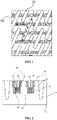
- the semiconductor structure includes: a substrate 10, the substrate 10 including an isolation structure 11 and an active region 12, and the active region 12 including ions of a first type; a trench 20, the trench 20 being arranged in the active region 12, an inner surface of the trench 20 including an inversion doping layer 30 and an oxide layer 40 which are arranged adjacent to each other, and the inversion doping layer 30 being arranged above the oxide layer 40; and a word line 50, the word line 50 being arranged in the trench 20.
- the inversion doping layer 30 includes ions of a second type. The first type is contrary to the second type.
- the inversion doping layer 30 with a doping type contrary to a doping type of the active region 12 is formed in a wall of the trench 20, so as to form a shallow junction (i.e., a PN junction) to fix the active region 12 and offset part of the drain voltage, so that a peak electric field of a drain depletion region is improved, and a hot carrier tunneling is improved, thereby improving the performance of the semiconductor structure.
- a shallow junction i.e., a PN junction
- the inversion doping layer 30 is configured to form a side wall of the trench 20, and the oxide layer 40 is configured to form a side wall and a bottom wall of the trench 20.
- the word line 50 is filled in the trench 20, so as to form an embedded word line 50.
- doping types can be understood as doping with P-type ions and N-type ions respectively, that is, doping with P-type ions and N-type ions corresponding to group III elements and group V elements.
- the irons of the first type are P-type ions or N-type ions, it is consistent with properties of a Metal Oxide Semiconductor Field Effect Transistor, MOSFET. That is, the first type of an NMOS is an N-type ion, and the first type of a PMOS is a P-type ion.
- the substrate 10 may be a P-type silicon substrate or an N-type silicon substrate.
- N-type ions ions of group V elements, such as phosphorus P or arsenic As
- the ions of the first type are the N-type ions
- the ions of the second type are the P-type ions (ions of group III elements, such as boron B or gallium Ga).
- P-type ions are implanted to the wall of the trench 20 to form the inversion doping layer 30.
- the P-type ions may also be boron di-fluoride BF2.
- the substrate 10 is of the P type
- P-type ions ions of group III elements, such as boron B or gallium Ga
- the ions of the first type are the P-type ions
- the ions of the second type are the N-type ions (ions of group V elements, such as phosphorus P or arsenic As).
- N-type ions are implanted to the wall of the trench 20 to form the inversion doping layer 30.
- a plurality of active regions 12 are provided in the substrate 10.
- the active regions 12 are filled between two adjacent isolation structures 11.
- a depth of each isolation structure 11 may be the same, or different from each other. It can be seen in combination with FIG. 1 that each word line 50 crosses over the plurality of active region 12. There are multiple word lines 50.
- the plurality of active regions 12 are arranged in multiple rows parallel to each other.
- Each word line 50 crosses over the multiple rows of active regions 12. The distance between the sides of two adjacent active regions 12 in two adjacent rows is relatively small, while the distance between the ends of two adjacent active regions 12 in the same row is relatively large.
- the active region 12 includes a source region and a drain region. Referring to FIG. 2 , the drain region is arranged between two adjacent word lines 50, and the source region is arranged between the isolation structure 11 and the word line 50.
- the isolation structure 11 may include silicon oxide, such as SIO2.
- the oxide layer 40 may include SIO2.
- a thickness of the oxide layer 40 is comprised between 3 nm and 8 nm.
- an inner surface of the trench 20 further includes a protective layer 60.
- the protective layer 60 is in contact with the inversion doping layer 30.
- the inversion doping layer 30 is sandwiched between a bottom end of the protective layer 60 and a top end of the oxide layer 40.
- the protective layer 60 is configured to protect the inversion doping layer 30, so as to prevent the inversion doping layer 30 from being damaged during the manufacturing process of the semiconductor structure.
- the protective layer 60 forms a side wall of the trench 20. That is, the protective layer 60 covers a portion of the inversion doping layer 30, so that the uncovered inversion doping layer 30 is sandwiched between the bottom end of the protective layer 60 and the top end of the oxide layer 40, thereby forming the side wall of the trench 20.
- the protective layer 60 may be SIO2, SIN, or a combination thereof.
- a thickness of the protective layer 60 is comprised between 3 nm and 10 nm.
- the inversion doping layer 30 includes a side wall section 31 in contact with the protective layer 60, and a bottom wall section 32 sandwiched between the bottom end of the protective layer 60 and the top end of the oxide layer 40.
- the bottom wall section 32 is perpendicular to the side wall section 31.
- the protective layer 60, the bottom wall section 32 and the oxide layer 40 form the inner surface of the trench 20.
- the inversion doping layer 30 is composed of the side wall section 31 and the bottom wall section 32.
- the protective layer 60 completely covers the side wall section 31, and the bottom end of the protective layer 60 is in contact with the bottom wall section 32, so that the protective layer 60, the bottom wall section 32 and the oxide layer 40 form the inner surface of the trench 20.
- the inversion doping layer 30 and the oxide layer 40 may be formed in the substrate 10. That is, the inversion doped layer 30 may be formed by implanting the ions of the second type to the substrate 10 (an implantation dose of the ions of the second type is comprised between 5E13/cm 2 and 1.5E14/cm 2 , and implantation energy of the ions of the second type is comprised between 0.5 KeV and 5 KeV).
- the oxide layer 40 may be formed in the substrate 10 through an In-Situ Steam Generation, ISSG, process.
- the protective layer 60 is formed on the surface of the substrate 10.
- the protective layer 60 may be formed on the substrate 10 through a Physical Vapor Deposition, PVD, process, a Chemical Vapor Deposition, CVD, process or an Atomic Layer Deposition, ALD, process.
- the inversion doped layer 30 may be formed by implanting the ions of the second type to the substrate 10.
- the oxide layer 40 may be formed on the surface of the substrate 10.
- the oxide layer 40 may be formed on the substrate 10 through the Physical Vapor Deposition process, the Chemical Vapor Deposition process or the Atomic Layer Deposition process.
- the protective layer 60 is formed on the surface of the substrate 10.
- the protective layer 60 may be formed on the substrate 10 through the Physical Vapor Deposition process, the Chemical Vapor Deposition process or the Atomic Layer Deposition process.
- the bottom end of the protective layer 60 is in contact with the bottom wall section 32, and the top end of the oxide layer 40 is in contact with the bottom wall section 32, so that the protective layer 60, the bottom wall section 32 and the oxide layer 40 form the inner surface of the trench 20.
- the projection of each of the side wall of the protective layer 60, the side wall of the bottom wall section 32, and the side wall of the oxide layer 40 facing to the substrate 10 coincide with each other. That is, the word line 50 in the trench 20 is of a structure with a constant cross-sectional area.
- the trench 20 is a circular hole
- a diameter of the circular hole remains unchanged along an extending direction of the circular hole, thereby facilitating the manufacture of the semiconductor structure.
- the word line 50 includes: a barrier layer 51, the barrier layer 51 being arranged on the surface of the oxide layer 40; and a conductive layer 52, the conductive layer 52 being arranged on a surface of the barrier layer 51.
- the arrangement of the barrier layer 51 can prevent diffusion of the conductive material forming the conductive layer 52.
- the semiconductor structure further includes an insulation layer 53.
- the insulation layer 53 is arranged above the barrier layer 51 and the conductive layer 52. Each of a top end of the barrier layer 51 and a top end of the conductive layer 52 is in contact with a bottom end of the insulation layer 53.
- the insulation layer 53 is configured to form a good insulation structure.
- the barrier layer 51 may include Ta, Ti, Ru, TaN, TiN, RuTa, RuTaN, W, Ir, or the like.
- the barrier layer 51 may be made of any other materials that prevent the conductive material layer from diffusing.
- a thickness of the barrier layer 51 may be comprised between 2 nm and 7 nm.
- the conductive layer 52 may be made of a metal material, such as Cu, Al, W or alloy thereof.
- the insulation layer 53 may be formed of a material including silicon oxide, silicon nitride, or a combination thereof.
- the insulation layer 53 may be SIN, SION, or SIO2.
- the barrier layer 51 covers a side wall and a bottom wall of the oxide layer 40. A plane where the top end of the barrier layer 51 is located is lower than a plane where the bottom end of the protective layer 60 is located.
- the plane where the top end of the barrier layer 51 is located is 10 nm to 20 nm lower than the plane where the bottom end of the protective layer 60 is located.
- the barrier layer 51 completely covers a side surface and a bottom surface of the conductive layer 52, so as to ensure an effective barrier effect.
- the top end of the conductive layer 52 and the top end of the barrier layer 51 are not in the same plane.
- the top end of the conductive layer 52 is higher than the top end of the barrier layer 51.
- the top end of the barrier later 51 is flush with the top end of the conductive layer 52. That is, the bottom end of the insulation layer 53 is a plane, so that the bottom end of the insulation layer is reliably in contact with the top end of the barrier later 51 and the top end of the conductive layer 52.
- the barrier layer 51 is arranged on the oxide layer 40, that is, the barrier layer 51 is arranged below the inversion doping layer 30.
- the top end of the barrier layer 51 may be flush with the top end of the oxide layer 40, or the top end of the barrier layer 51 is lower than the top end of the oxide layer 40. Therefore, the insulation layer 53 completely covers the protective layer 60 and the bottom wall section 32 of the inversion doping layer 30.
- One embodiment of the application further provides a method for manufacturing a semiconductor structure.
- the method for manufacturing the semiconductor structure includes the following operations.
- a substrate 10 including an isolation structure 11 and an active region 12 is provided.
- the active region 12 is doped with ions of a first type.
- a trench 20 is formed in the active region 12.
- An inversion doping layer 30 and an oxide layer 40 are formed in the trench 20.
- the inversion doping layer 30 is arranged above the oxide layer 40.
- a word line 50 is formed in the trench 20.
- the inversion doping layer 30 is doped with ions of a second type.
- the first type is contrary to the second type.
- the inversion doping layer 30 with a doping type contrary to a doping type of the active region 12 is formed in a wall of the trench 20, so as to form a shallow junction (i.e., a PN junction) to fix the active region 12 and offset part of the drain voltage, so that a peak electric field of a drain depletion region is improved, and a hot carrier tunneling is improved, thereby improving the performance of the semiconductor structure.
- a shallow junction i.e., a PN junction
- the provided substrate 10 is a substrate 10 including an isolation structure 11 and an active region 12. That is, the trench 20 is directly formed on the substrate 10 without considering a specific forming method of the isolation structure 11 and the active region 12, and the word line 50 is formed.
- the substrate 10 may be planarized through dry etching or Chemical Mechanical Polishing, CMP.
- An upper surface of the substrate 10 may be provided with a layer of protective structure, such as an oxide layer.
- the word line 50 is an embedded word line.
- the operation that the trench 20 is formed in the active region 12 includes the following operations.
- a first groove 70 is formed in the active region 12.
- the ions of the second type are implanted to an inner surface of the first groove 70 to form an ion implantation region 71.
- a surface of the ion implantation region 71 is covered with a protective material layer 77.
- a bottom portion of the protective material layer 77, a bottom portion of the ion implantation region 71 and a bottom portion of the first groove 70 are etched to form a second groove 72.
- a remaining part of the ion implantation region 71 is configured as the inversion doping layer 30, and a remaining part of the protective material layer 77 is configured as a protective layer 60.
- the oxide layer 40 is formed on an inner surface of the second groove 72.
- the protective layer 60, the inversion doping layer 30 and the oxide layer 40 form an inner surface of the trench 20.
- the first groove 70 and the second groove 72 should be sequentially formed. Furthermore, an inner surface of the first groove 70 is treated with the ions of the second type and the protective material layer 77, and the oxide layer 40 is formed on the inner surface of the second groove 72, thereby forming the inner surface of the trench 20.
- a depth of the first groove 70 is comprised between 30 nm and 80 nm, and/or a depth of the second groove 72 is comprised between 50 nm and 100 nm.
- the method further includes the following operations.
- the protective material layer 77 is formed to cover the inner surface of the first groove 70 and a surface of the substrate 10.
- the protective material layer 77 on the surface of the substrate 10 and at the bottom portion of the first groove 70 is etched, so as to expose the substrate 10 and the ion implantation region 71.
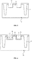
- the formation of the trench 20 is described with reference to FIG. 4 to FIG. 9 .
- the substrate 10 including the isolation structure 11 and the active region 12 is provided.
- the first groove 70 is formed on the substrate 10. That is, the first groove 70 is formed in the active region 12.
- the depth of the first groove 70 may be comprised between 30 nm and 80 nm, and a width of the first groove is comprised between 30 nm and 60 nm.
- the process of the first groove 70 is not limited, and a proper process in the related technology can be used, such as etching.
- the ions of the second type are implanted to the substrate 10 via the first groove 70, so that the ion implantation region 71 is formed in the substrate 10.
- the ion implantation region 71 forms the inner surface of the first groove 70.
- the ions of the second type are P-type ions, such as boron B, gallium Ga, and boron di-fluoride BF2.
- the ions of the second type are N-type ions, such as phosphorus P or arsenic As.
- the protective material layer 77 is formed through the Physical Vapor Deposition process, the Chemical Vapor Deposition process or the Atomic Layer Deposition process.
- the protective material layer 77 covers the inner surface of the first groove 70 and an upper surface of the substrate 10.
- the protective material layer 77 may be SIO2, SIN, or a combination thereof.
- the thickness of the protective material layer 77 is comprised between 3 nm and 10 nm.
- the protective material layer 77 covering the upper surface of the substrate 10 is etched to expose the upper surface of the substrate 10.
- the protective material layer 77 is etched in an extending direction of the first groove 70. That is, only the protective material layer 77 extending in a vertical direction is remained.
- the protective material layer is continuously etched downward until the second groove 72 is formed. In this case, the remaining part of the ion implantation region 71 is configured as the inversion doping layer 30.
- the second groove 72 is formed below the first groove 70.
- the depth of the second groove 72 may be comprised between 50 nm and 100 nm, and a width of the second groove may be comprised between 15 nm and 50 nm.
- the oxide layer 40 is formed on the inner surface of the second groove 72 through the In-Situ Steam Generation process.
- the trench 20 is formed.
- the oxide layer 40 includes SIO2, and the thickness of the oxide layer 40 may be comprised between 3 nm and 8 nm.
- an implantation dose of the ions of the second type is comprised between 5E13/cm 2 and 1.5E14/cm 2
- implantation energy of the ions of the second type is comprised between 0.5 KeV and 5 KeV.
- the operation that the word line 50 is formed in the trench 20 includes the following operations.
- a barrier material layer 73 is formed to cover the inner surface of the trench 20.
- a conductive material layer 74 is formed on a surface of the barrier material layer 73, and the trench 20 is filled.
- the conductive material layer 74 and the barrier material layer 73 are etched to sequentially expose the protective layer 60 and the inversion doping layer 30 between the protective layer 60 and the oxide layer 40, so as to form a third groove 75.
- a remaining part of the conductive material layer 74 is configured as a conductive layer 52, and a remaining part of the barrier material layer 73 is configured as a barrier layer 51.
- An insulation material layer 76 is formed on an inner surface of the third groove 75 and a surface of the substrate 10.
- the insulation material layer 76 on the surface of the substrate 10 is etched to expose a top end of the inversion doping layer 30 and a top end of the protective layer 60. A remaining part of the insulation material layer 76 is configured as an insulation layer 53.
- the barrier layer 51 and the conductive layer 52 form the word line 50, and the insulation layer 53 is arranged above the word line 50.
- the barrier layer 51, the conductive layer 52 and the insulation layer 53 should be formed sequentially.
- a depth of the third groove 75 is 10 nm to 20 nm greater than a depth of the first groove 70.
- the depth of the third groove 75 is comprised between 40 nm and 80 nm.
- the forming process of the word line 50 is described with reference to FIG. 10 to FIG. 13 .
- the barrier material layer 73 is formed through the Physical Vapor Deposition process, the Chemical Vapor Deposition process or the Atomic Layer Deposition process.
- the barrier material layer 73 covers the inner surface of the trench 20 and the upper surface of the substrate 10.
- the barrier material layer 73 may include Ta, Ti, Ru, TaN, TiN, RuTa, RuTaN, W, or Ir.
- the barrier material layer 73 may be made of any other material that prevents the conductive material layer from diffusing.
- the thickness of the barrier material layer 73 may be comprised between 2 nm and 7 nm.
- the conductive material layer 74 is formed through the Physical Vapor Deposition process, the Chemical Vapor Deposition process or the Atomic Layer Deposition process.
- the conductive material layer 74 is filled in a space formed by the barrier material layer 73 and covers the barrier material layer 73 arranged on the upper surface of the substrate 10.
- the upper surface of the conductive material layer 74 is planatized through dry etching or Chemical Mechanical Polishing, CMP.
- the conductive layer 52 may be made of a metal material, such as Cu, Al, W or alloy thereof.
- the conductive material layer 74 and the barrier material layer 73 on the upper surface of the substrate 10 are etched, and the conductive material layer 74 and the barrier material layer 73 in the trench 20 are etched, so as to expose the bottom wall section 32 of the inversion doping layer 30.
- the remaining part of the conductive material layer 74 is configured as the conductive layer 52
- the remaining part of the barrier material layer 73 is configured as the barrier layer 51.
- the third groove 75 is formed above the conductive layer 52 and the barrier layer 51.
- the depth of the third groove 75 may be comprised between 40 nm and 80 nm. That is, the bottom end of the third groove 75 should be lower than the bottom end of the first groove 70.
- the depth of the third groove 75 is 10 nm to 20 nm greater than the depth of the first groove 70.
- the insulation material layer 76 is formed through the Physical Vapor Deposition process, the Chemical Vapor Deposition process or the Atomic Layer Deposition process.
- the insulation material layer 76 is filled in the third groove 75 and covers the upper surface of the substrate 10.
- the insulation material layer 76 may be SIN, SION or SIO2.
- the insulation material layer 76 is planarized through dry etching or Chemical Mechanical Polishing. Finally, the insulation material layer 76 is etched. The remaining part of the insulation material layer 76 is configured as the insulation layer 53, and the semiconductor structure as shown in FIG. 2 is formed.
- the upper surface of the substrate 10 may be provided with a protective structure.
- the protective structure should be removed.
- the protective structure as well as the protective material layer 77 and the insulation material layer 76 in the protective structure should also be removed.
Landscapes
- Engineering & Computer Science (AREA)
- Manufacturing & Machinery (AREA)
- Semiconductor Memories (AREA)
- Element Separation (AREA)
Abstract
Description
- This application claims priority to
Chinese Patent Application No. 202010816422.1, filed on August 14, 2020 - The application relates to the technical field of a semiconductor, in particular to a semiconductor structure and a method for manufacturing the semiconductor structure.
- A Dynamic Random Access Memory, DRAM is a common semiconductor device in an electronic device such as a computer, and includes a memory cell array for storing data and a peripheral circuit arranged on a periphery of the memory cell array. Each memory cell usually includes a transistor (word line), a bit line and a capacitor. A word line voltage on the transistor (word line) can control turning on and turning off of the transistor, so that the data information stored in the capacitor can be read on the bit line, or the data information can be written into the capacitor through the bit line.
- With the development of the manufacturing process, a feature size of a Metal Oxide Semiconductor, MOS is continuously reduced, and the intensity of a transverse electric field of a channel of an MOS device is continuously enhanced. During operation of a semiconductor word line transistor (for example, an N-channel Metal Oxide Semiconductor, NMOS), due to the combined effect of a drain voltage (Vdd) and a gate voltage (Vg), a strong electric field is formed near the drain, so that the damage of a hot carrier to the device mainly occurs in an oxide layer close to the drain, thereby resulting in a drift of a switching characteristic of a transistor switch and serious degradation of reliability of the device.
- The application provides a semiconductor structure and a method for manufacturing the semiconductor structure, so as to improve the performance of the semiconductor structure.
- According to a first aspect of the application, a semiconductor structure is provided, which includes:
- a substrate including an isolation structure and an active region, the active region including ions of a first type;
- a trench arranged in the active region, an inner surface of the trench including an inversion doping layer and an oxide layer which are arranged adjacent to each other, and the inversion doping layer being arranged above the oxide layer; and
- a word line arranged in the trench.
- The inversion doping layer includes ions of a second type. The first type is contrary to the second type.
- In one embodiment of the application, the inner surface of the trench further includes:
a protective layer in contact with the inversion doping layer, the inversion doping layer being sandwiched between a bottom end of the protective layer and a top end of the oxide layer. - In one embodiment of the application, the inversion doping layer includes:
- a side wall section in contact with the protective layer; and
- a bottom wall section sandwiched between the bottom end of the protective layer and the top end of the oxide layer, the bottom wall section being perpendicular to the side wall section.
- The protective layer, the bottom wall section and the oxide layer form the inner surface of the trench.
- In one embodiment of the application, each of the bottom end of the protective layer and the top end of the oxide layer is in contact with the bottom wall section.
- In one embodiment of the application, the word line includes:
- a barrier layer arranged on a surface of the oxide layer; and
- a conductive layer arranged on a surface of the barrier layer.
- In one embodiment of the application, the semiconductor structure further includes:
an insulation layer arranged above the barrier layer and the conductive layer, each of a top end of the barrier layer and a top end of the conductive layer being in contact with a bottom end of the insulation layer. - The barrier layer covers a side wall and a bottom wall of the oxide layer, and a plane where the top end of the barrier layer is located is lower than a plane where the bottom end of the protective layer is located.
- In one embodiment of the application, the plane where the top end of the barrier layer is located is 10 nm to 20 nm lower than the plane where the bottom end of the protective layer is located.
- In one embodiment of the application, a top end of the barrier layer is flush with a top end of the conductive layer.
- According to a second aspect of the application, a method for manufacturing a semiconductor structure is provided, which includes the following operations.
- A substrate including an isolation structure and an active region is provided, in which the active region is doped with ions of a first type.
- A trench is formed in the active region, in which an inversion doping layer and an oxide layer are formed in the trench, and the inversion doping layer is arranged above the oxide layer.
- A word line is formed in the trench.
- The inversion doping layer is doped with ions of a second type. The first type is contrary to the second type.
- In one embodiment of the application, the operation that the trench is formed in the active region includes the following operations.
- A first groove is formed in the active region.
- The ions of the second type are implanted to an inner surface of the first groove to form an ion implantation region.
- A surface of the ion implantation region is covered with a protective material layer.
- A bottom portion of the protective material layer, a bottom portion of the ion implantation region and a bottom portion of the first groove are etched, so as to form a second groove. A remaining part of the ion implantation region is configured as the inversion doping layer, and a remaining part of the protective material layer is configured as a protective layer.
- The oxide layer is formed on an inner surface of the second groove.
- The protective layer, the inversion doping layer and the oxide layer form an inner surface of the trench.
- In one embodiment of the application, a depth of the first groove is comprised between 30 nm and 80 nm, and/or a depth of the second groove is comprised between 50 nm and 100 nm.
- In one embodiment of the application, after the ion implantation region is formed and before the second groove is formed, the method further includes the following operations.
- The protective material layer is formed to cover the inner surface of the first groove and a surface of the substrate.
- The protective material layer on the surface of the substrate and at the bottom portion of the first groove is etched, so as to expose the substrate and the ion implantation region.
- In one embodiment of the application, the operation that the word line is formed in the trench includes the following operations.
- A barrier material layer is formed to cover the inner surface of the trench.
- A conductive material layer is formed on a surface of the barrier material layer, and the trench is filled.
- The conductive material layer and the barrier material layer are etched to sequentially expose the protective layer and the inversion doping layer between the protective layer and the oxide layer, so as to form a third groove. A remaining part of the conductive material layer is configured as a conductive layer, and a remaining part of the barrier material layer is configured as a barrier layer.
- An insulation material layer is formed on an inner surface of the third groove and a surface of the substrate.
- The insulation material layer on the surface of the substrate is etched to expose a top end of the inversion doping layer and a top end of the protective layer. A remaining part of the insulation material layer is configured as an insulation layer.
- The barrier layer and the conductive layer form the word line, and the insulation layer is arranged above the word line.
- In one embodiment of the application, a depth of the third groove is 10 nm to 20 nm greater than a depth of the first groove.
- In one embodiment of the application, an implantation dose of the ions of the second type is comprised between 5E13/cm2 and 1.5E14/cm2, and implantation energy of the ions of the second type is comprised between 0.5 KeV and 5 KeV.
- According to the semiconductor structure of the application, the inversion doping layer with a doping type contrary to a doping type of the active region is formed in a wall of the trench, so as to form a shallow junction (i.e., a PN junction) to fix the active region and offset part of the drain voltage, so that a peak electric field of a drain depletion region is improved, and a hot carrier tunneling is improved, thereby improving the performance of the semiconductor structure.
- By considering the following detailed description of the preferred implementations of the application in conjunction with the accompanying drawings, various objectives, features, and advantages of the application will become more apparent. The drawings are merely exemplary illustrations of the application, and are not necessarily drawn to scale. In the drawings, the same reference numerals always denote the same or similar parts, in which:
-
FIG. 1 is a schematic diagram of a semiconductor structure according to an exemplary embodiment; -
FIG. 2 is a schematic diagram of a portion A-A inFIG. 1 ; -
FIG. 3 is a flowchart of a method for manufacturing a semiconductor structure according to one exemplary embodiment; -
FIG. 4 is a schematic diagram of a substrate provided in a method for manufacturing a semiconductor structure according to one exemplary embodiment; -
FIG. 5 is a schematic diagram after forming a first groove in a method for manufacturing a semiconductor structure according to one exemplary embodiment; -
FIG. 6 is a schematic diagram after forming an ion implantation region in a method for manufacturing a semiconductor structure according to one exemplary embodiment; -
FIG. 7 is a schematic diagram after covering a protective material layer in a method for manufacturing a semiconductor structure according to one exemplary embodiment; -
FIG. 8 is a schematic diagram after forming a second groove in a method for manufacturing a semiconductor structure according to one exemplary embodiment; -
FIG. 9 is a schematic diagram after forming an oxide layer in a method for manufacturing a semiconductor structure according to one exemplary embodiment; -
FIG. 10 is a schematic diagram after covering a barrier material layer in a method for manufacturing a semiconductor structure according to one exemplary embodiment; -
FIG. 11 is a schematic diagram after covering a conductive material layer in a method for manufacturing a semiconductor structure according to one exemplary embodiment; -
FIG. 12 is a schematic diagram after forming a third groove in a method for manufacturing a semiconductor structure according to one exemplary embodiment; and -
FIG. 13 is a schematic diagram after covering an insulation material layer in a method for manufacturing a semiconductor structure according to one exemplary embodiment. - 10: substrate; 11: isolation structure; 12: active region; 20: trench; 30: inversion doping layer; 31: side wall section; 32: bottom wall section; 40: oxide layer; 50: word line; 51: barrier layer; 52: conductive layer; 53: insulation layer; 60: protective layer; 70: first groove; 71: ion implantation region; 72: second groove; 73: barrier material layer; 74: conductive material layer; 75: third groove; 77: protective material layer; 76: insulation material layer.
- Typical embodiments embodying features and advantages of the application will be described in detail in the following description. It should be understood that there may be various changes in different embodiments of the application, all of which do not depart from the scope of the application. The descriptions and drawings therein are illustrative in nature, and are not intended to limit the application.
- The following description of different exemplary embodiments of the application is made with reference to the accompanying drawings, which form a part of the application, and in which different exemplary structures, systems and steps that can implement various aspects of the application are shown by way of example. It should be understood that structures and functions may be modified by using other specific solutions of components, structures, exemplary devices, systems, and steps without departing from the scope of the application. Moreover, although the terms "above", "between", "within", or the like may be used in the specification to describe different exemplary features and elements of the application, these terms are used herein for convenience of description only, for example, according to directions of examples described in the drawings. Nothing in the specification should be understood as requiring a specific three-dimensional orientation of the structure to fall within the scope of the application.
- One embodiment of the application provides a semiconductor structure. Referring to
FIG. 1 , the semiconductor structure includes: asubstrate 10, thesubstrate 10 including anisolation structure 11 and anactive region 12, and theactive region 12 including ions of a first type; atrench 20, thetrench 20 being arranged in theactive region 12, an inner surface of thetrench 20 including aninversion doping layer 30 and anoxide layer 40 which are arranged adjacent to each other, and theinversion doping layer 30 being arranged above theoxide layer 40; and aword line 50, theword line 50 being arranged in thetrench 20. Theinversion doping layer 30 includes ions of a second type. The first type is contrary to the second type. - According to the semiconductor structure of one embodiment of the application, the
inversion doping layer 30 with a doping type contrary to a doping type of theactive region 12 is formed in a wall of thetrench 20, so as to form a shallow junction (i.e., a PN junction) to fix theactive region 12 and offset part of the drain voltage, so that a peak electric field of a drain depletion region is improved, and a hot carrier tunneling is improved, thereby improving the performance of the semiconductor structure. - It should be noted that the
inversion doping layer 30 is configured to form a side wall of thetrench 20, and theoxide layer 40 is configured to form a side wall and a bottom wall of thetrench 20. Theword line 50 is filled in thetrench 20, so as to form an embeddedword line 50. - It should be noted that the contrary doping types can be understood as doping with P-type ions and N-type ions respectively, that is, doping with P-type ions and N-type ions corresponding to group III elements and group V elements. Regarding whether the irons of the first type are P-type ions or N-type ions, it is consistent with properties of a Metal Oxide Semiconductor Field Effect Transistor, MOSFET. That is, the first type of an NMOS is an N-type ion, and the first type of a PMOS is a P-type ion.
- Specifically, the
substrate 10 may be a P-type silicon substrate or an N-type silicon substrate. - For example, if the
substrate 10 is of the N type, N-type ions (ions of group V elements, such as phosphorus P or arsenic As) are implanted to the silicon substrate to form theactive region 12. If the ions of the first type are the N-type ions, the ions of the second type are the P-type ions (ions of group III elements, such as boron B or gallium Ga). In this case, P-type ions are implanted to the wall of thetrench 20 to form theinversion doping layer 30. The P-type ions may also be boron di-fluoride BF2. - Alternatively, if the
substrate 10 is of the P type, P-type ions (ions of group III elements, such as boron B or gallium Ga) are implanted to the silicon substrate to form theactive region 12. If the ions of the first type are the P-type ions, the ions of the second type are the N-type ions (ions of group V elements, such as phosphorus P or arsenic As). In this case, N-type ions are implanted to the wall of thetrench 20 to form theinversion doping layer 30. - In one embodiment, as shown in
FIG. 1 and FIG. 2 , a plurality ofactive regions 12 are provided in thesubstrate 10. Theactive regions 12 are filled between twoadjacent isolation structures 11. A depth of eachisolation structure 11 may be the same, or different from each other. It can be seen in combination withFIG. 1 that eachword line 50 crosses over the plurality ofactive region 12. There are multiple word lines 50. - In one embodiment, referring to
FIG. 1 , the plurality ofactive regions 12 are arranged in multiple rows parallel to each other. Eachword line 50 crosses over the multiple rows ofactive regions 12. The distance between the sides of two adjacentactive regions 12 in two adjacent rows is relatively small, while the distance between the ends of two adjacentactive regions 12 in the same row is relatively large. - In one embodiment, the
active region 12 includes a source region and a drain region. Referring toFIG. 2 , the drain region is arranged between two adjacent word lines 50, and the source region is arranged between theisolation structure 11 and theword line 50. - In one embodiment, the
isolation structure 11 may include silicon oxide, such as SIO2. - In one embodiment, the
oxide layer 40 may include SIO2. - In one embodiment, a thickness of the
oxide layer 40 is comprised between 3 nm and 8 nm. - In one embodiment, as shown in
FIG. 2 , an inner surface of thetrench 20 further includes aprotective layer 60. Theprotective layer 60 is in contact with theinversion doping layer 30. Theinversion doping layer 30 is sandwiched between a bottom end of theprotective layer 60 and a top end of theoxide layer 40. Theprotective layer 60 is configured to protect theinversion doping layer 30, so as to prevent theinversion doping layer 30 from being damaged during the manufacturing process of the semiconductor structure. - It should be noted that the
protective layer 60 forms a side wall of thetrench 20. That is, theprotective layer 60 covers a portion of theinversion doping layer 30, so that the uncoveredinversion doping layer 30 is sandwiched between the bottom end of theprotective layer 60 and the top end of theoxide layer 40, thereby forming the side wall of thetrench 20. - In one embodiment, the
protective layer 60 may be SIO2, SIN, or a combination thereof. - In one embodiment, a thickness of the
protective layer 60 is comprised between 3 nm and 10 nm. - In one embodiment, as shown in
FIG. 2 , theinversion doping layer 30 includes aside wall section 31 in contact with theprotective layer 60, and abottom wall section 32 sandwiched between the bottom end of theprotective layer 60 and the top end of theoxide layer 40. Thebottom wall section 32 is perpendicular to theside wall section 31. Theprotective layer 60, thebottom wall section 32 and theoxide layer 40 form the inner surface of thetrench 20. - The
inversion doping layer 30 is composed of theside wall section 31 and thebottom wall section 32. Theprotective layer 60 completely covers theside wall section 31, and the bottom end of theprotective layer 60 is in contact with thebottom wall section 32, so that theprotective layer 60, thebottom wall section 32 and theoxide layer 40 form the inner surface of thetrench 20. - It should be noted that the
inversion doping layer 30 and theoxide layer 40 may be formed in thesubstrate 10. That is, the inversion dopedlayer 30 may be formed by implanting the ions of the second type to the substrate 10 (an implantation dose of the ions of the second type is comprised between 5E13/cm2 and 1.5E14/cm2, and implantation energy of the ions of the second type is comprised between 0.5 KeV and 5 KeV). Theoxide layer 40 may be formed in thesubstrate 10 through an In-Situ Steam Generation, ISSG, process. Theprotective layer 60 is formed on the surface of thesubstrate 10. For example, theprotective layer 60 may be formed on thesubstrate 10 through a Physical Vapor Deposition, PVD, process, a Chemical Vapor Deposition, CVD, process or an Atomic Layer Deposition, ALD, process. - Alternatively, the inversion doped
layer 30 may be formed by implanting the ions of the second type to thesubstrate 10. Theoxide layer 40 may be formed on the surface of thesubstrate 10. For example, theoxide layer 40 may be formed on thesubstrate 10 through the Physical Vapor Deposition process, the Chemical Vapor Deposition process or the Atomic Layer Deposition process. Correspondingly, theprotective layer 60 is formed on the surface of thesubstrate 10. For example, theprotective layer 60 may be formed on thesubstrate 10 through the Physical Vapor Deposition process, the Chemical Vapor Deposition process or the Atomic Layer Deposition process. - In one embodiment, the bottom end of the
protective layer 60 is in contact with thebottom wall section 32, and the top end of theoxide layer 40 is in contact with thebottom wall section 32, so that theprotective layer 60, thebottom wall section 32 and theoxide layer 40 form the inner surface of thetrench 20. - In one embodiment, the projection of each of the side wall of the
protective layer 60, the side wall of thebottom wall section 32, and the side wall of theoxide layer 40 facing to thesubstrate 10 coincide with each other. That is, theword line 50 in thetrench 20 is of a structure with a constant cross-sectional area. - Specifically, for example, if the
trench 20 is a circular hole, a diameter of the circular hole remains unchanged along an extending direction of the circular hole, thereby facilitating the manufacture of the semiconductor structure. - In one embodiment, as shown in
FIG. 2 , theword line 50 includes: abarrier layer 51, thebarrier layer 51 being arranged on the surface of theoxide layer 40; and aconductive layer 52, theconductive layer 52 being arranged on a surface of thebarrier layer 51. The arrangement of thebarrier layer 51 can prevent diffusion of the conductive material forming theconductive layer 52. - In one embodiment, as shown in
FIG. 2 , the semiconductor structure further includes aninsulation layer 53. Theinsulation layer 53 is arranged above thebarrier layer 51 and theconductive layer 52. Each of a top end of thebarrier layer 51 and a top end of theconductive layer 52 is in contact with a bottom end of theinsulation layer 53. Theinsulation layer 53 is configured to form a good insulation structure. - In one embodiment, the
barrier layer 51 may include Ta, Ti, Ru, TaN, TiN, RuTa, RuTaN, W, Ir, or the like. Thebarrier layer 51 may be made of any other materials that prevent the conductive material layer from diffusing. - In one embodiment, a thickness of the
barrier layer 51 may be comprised between 2 nm and 7 nm. - In one embodiment, the
conductive layer 52 may be made of a metal material, such as Cu, Al, W or alloy thereof. - In one embodiment, the
insulation layer 53 may be formed of a material including silicon oxide, silicon nitride, or a combination thereof. For example, theinsulation layer 53 may be SIN, SION, or SIO2. - In one embodiment, the
barrier layer 51 covers a side wall and a bottom wall of theoxide layer 40. A plane where the top end of thebarrier layer 51 is located is lower than a plane where the bottom end of theprotective layer 60 is located. - Specifically, the plane where the top end of the
barrier layer 51 is located is 10 nm to 20 nm lower than the plane where the bottom end of theprotective layer 60 is located. - In one embodiment, the
barrier layer 51 completely covers a side surface and a bottom surface of theconductive layer 52, so as to ensure an effective barrier effect. - In one embodiment, the top end of the
conductive layer 52 and the top end of thebarrier layer 51 are not in the same plane. For example, the top end of theconductive layer 52 is higher than the top end of thebarrier layer 51. - In one embodiment, the top end of the barrier later 51 is flush with the top end of the
conductive layer 52. That is, the bottom end of theinsulation layer 53 is a plane, so that the bottom end of the insulation layer is reliably in contact with the top end of the barrier later 51 and the top end of theconductive layer 52. - Specifically, through analysis in combination with
FIG. 2 , thebarrier layer 51 is arranged on theoxide layer 40, that is, thebarrier layer 51 is arranged below theinversion doping layer 30. The top end of thebarrier layer 51 may be flush with the top end of theoxide layer 40, or the top end of thebarrier layer 51 is lower than the top end of theoxide layer 40. Therefore, theinsulation layer 53 completely covers theprotective layer 60 and thebottom wall section 32 of theinversion doping layer 30. - One embodiment of the application further provides a method for manufacturing a semiconductor structure. Referring to
FIG. 3 , the method for manufacturing the semiconductor structure includes the following operations. - In S101, a
substrate 10 including anisolation structure 11 and anactive region 12 is provided. Theactive region 12 is doped with ions of a first type. - In S103, a
trench 20 is formed in theactive region 12. Aninversion doping layer 30 and anoxide layer 40 are formed in thetrench 20. Theinversion doping layer 30 is arranged above theoxide layer 40. - In S105, a
word line 50 is formed in thetrench 20. - The
inversion doping layer 30 is doped with ions of a second type. The first type is contrary to the second type. - According to the method for manufacturing the semiconductor structure of one embodiment of the application, the
inversion doping layer 30 with a doping type contrary to a doping type of theactive region 12 is formed in a wall of thetrench 20, so as to form a shallow junction (i.e., a PN junction) to fix theactive region 12 and offset part of the drain voltage, so that a peak electric field of a drain depletion region is improved, and a hot carrier tunneling is improved, thereby improving the performance of the semiconductor structure. - It should be noted that as shown in
FIG. 4 , the providedsubstrate 10 is asubstrate 10 including anisolation structure 11 and anactive region 12. That is, thetrench 20 is directly formed on thesubstrate 10 without considering a specific forming method of theisolation structure 11 and theactive region 12, and theword line 50 is formed. Before thetrench 20 is formed, thesubstrate 10 may be planarized through dry etching or Chemical Mechanical Polishing, CMP. An upper surface of thesubstrate 10 may be provided with a layer of protective structure, such as an oxide layer. - It should be noted that the
word line 50 is an embedded word line. - In one embodiment, the operation that the
trench 20 is formed in theactive region 12 includes the following operations. Afirst groove 70 is formed in theactive region 12. The ions of the second type are implanted to an inner surface of thefirst groove 70 to form anion implantation region 71. A surface of theion implantation region 71 is covered with aprotective material layer 77. A bottom portion of theprotective material layer 77, a bottom portion of theion implantation region 71 and a bottom portion of thefirst groove 70 are etched to form asecond groove 72. A remaining part of theion implantation region 71 is configured as theinversion doping layer 30, and a remaining part of theprotective material layer 77 is configured as aprotective layer 60. Theoxide layer 40 is formed on an inner surface of thesecond groove 72. Theprotective layer 60, theinversion doping layer 30 and theoxide layer 40 form an inner surface of thetrench 20. - For the formation of the
trench 20, thefirst groove 70 and thesecond groove 72 should be sequentially formed. Furthermore, an inner surface of thefirst groove 70 is treated with the ions of the second type and theprotective material layer 77, and theoxide layer 40 is formed on the inner surface of thesecond groove 72, thereby forming the inner surface of thetrench 20. - In one embodiment, a depth of the
first groove 70 is comprised between 30 nm and 80 nm, and/or a depth of thesecond groove 72 is comprised between 50 nm and 100 nm. - In one embodiment, after the
ion implantation region 71 is formed and before thesecond groove 72 is formed, the method further includes the following operations. Theprotective material layer 77 is formed to cover the inner surface of thefirst groove 70 and a surface of thesubstrate 10. Theprotective material layer 77 on the surface of thesubstrate 10 and at the bottom portion of thefirst groove 70 is etched, so as to expose thesubstrate 10 and theion implantation region 71. - Specifically, the formation of the
trench 20 is described with reference toFIG. 4 to FIG. 9 . - As shown in
FIG. 4 , thesubstrate 10 including theisolation structure 11 and theactive region 12 is provided. - As shown in
FIG. 5 , thefirst groove 70 is formed on thesubstrate 10. That is, thefirst groove 70 is formed in theactive region 12. The depth of thefirst groove 70 may be comprised between 30 nm and 80 nm, and a width of the first groove is comprised between 30 nm and 60 nm. The process of thefirst groove 70 is not limited, and a proper process in the related technology can be used, such as etching. - As shown in
FIG. 6 , the ions of the second type are implanted to thesubstrate 10 via thefirst groove 70, so that theion implantation region 71 is formed in thesubstrate 10. Theion implantation region 71 forms the inner surface of thefirst groove 70. If thesubstrate 10 is of an N type, the ions of the second type are P-type ions, such as boron B, gallium Ga, and boron di-fluoride BF2. Alternatively, if thesubstrate 10 is of a P type, the ions of the second type are N-type ions, such as phosphorus P or arsenic As. - As shown in
FIG. 7 , theprotective material layer 77 is formed through the Physical Vapor Deposition process, the Chemical Vapor Deposition process or the Atomic Layer Deposition process. Theprotective material layer 77 covers the inner surface of thefirst groove 70 and an upper surface of thesubstrate 10. Theprotective material layer 77 may be SIO2, SIN, or a combination thereof. The thickness of theprotective material layer 77 is comprised between 3 nm and 10 nm. - As shown in
FIG. 8 , theprotective material layer 77 covering the upper surface of thesubstrate 10 is etched to expose the upper surface of thesubstrate 10. Theprotective material layer 77 is etched in an extending direction of thefirst groove 70. That is, only theprotective material layer 77 extending in a vertical direction is remained. After theion implantation region 71 in a horizontal direction is exposed, the protective material layer is continuously etched downward until thesecond groove 72 is formed. In this case, the remaining part of theion implantation region 71 is configured as theinversion doping layer 30. Thesecond groove 72 is formed below thefirst groove 70. The depth of thesecond groove 72 may be comprised between 50 nm and 100 nm, and a width of the second groove may be comprised between 15 nm and 50 nm. - As shown in
FIG. 9 , theoxide layer 40 is formed on the inner surface of thesecond groove 72 through the In-Situ Steam Generation process. In this case, thetrench 20 is formed. Theoxide layer 40 includes SIO2, and the thickness of theoxide layer 40 may be comprised between 3 nm and 8 nm. - In one embodiment, an implantation dose of the ions of the second type is comprised between 5E13/cm2 and 1.5E14/cm2, and implantation energy of the ions of the second type is comprised between 0.5 KeV and 5 KeV.
- In one embodiment, the operation that the
word line 50 is formed in thetrench 20 includes the following operations. Abarrier material layer 73 is formed to cover the inner surface of thetrench 20. Aconductive material layer 74 is formed on a surface of thebarrier material layer 73, and thetrench 20 is filled. Theconductive material layer 74 and thebarrier material layer 73 are etched to sequentially expose theprotective layer 60 and theinversion doping layer 30 between theprotective layer 60 and theoxide layer 40, so as to form athird groove 75. A remaining part of theconductive material layer 74 is configured as aconductive layer 52, and a remaining part of thebarrier material layer 73 is configured as abarrier layer 51. Aninsulation material layer 76 is formed on an inner surface of thethird groove 75 and a surface of thesubstrate 10. Theinsulation material layer 76 on the surface of thesubstrate 10 is etched to expose a top end of theinversion doping layer 30 and a top end of theprotective layer 60. A remaining part of theinsulation material layer 76 is configured as aninsulation layer 53. Thebarrier layer 51 and theconductive layer 52 form theword line 50, and theinsulation layer 53 is arranged above theword line 50. - For the forming process of the
word line 50, thebarrier layer 51, theconductive layer 52 and theinsulation layer 53 should be formed sequentially. - In one embodiment, a depth of the
third groove 75 is 10 nm to 20 nm greater than a depth of thefirst groove 70. - In one embodiment, the depth of the
third groove 75 is comprised between 40 nm and 80 nm. - Specifically, the forming process of the
word line 50 is described with reference toFIG. 10 to FIG. 13 . - As shown in
FIG. 10 , thebarrier material layer 73 is formed through the Physical Vapor Deposition process, the Chemical Vapor Deposition process or the Atomic Layer Deposition process. Thebarrier material layer 73 covers the inner surface of thetrench 20 and the upper surface of thesubstrate 10. Thebarrier material layer 73 may include Ta, Ti, Ru, TaN, TiN, RuTa, RuTaN, W, or Ir. Thebarrier material layer 73 may be made of any other material that prevents the conductive material layer from diffusing. The thickness of thebarrier material layer 73 may be comprised between 2 nm and 7 nm. - As shown in
FIG. 11 , theconductive material layer 74 is formed through the Physical Vapor Deposition process, the Chemical Vapor Deposition process or the Atomic Layer Deposition process. Theconductive material layer 74 is filled in a space formed by thebarrier material layer 73 and covers thebarrier material layer 73 arranged on the upper surface of thesubstrate 10. The upper surface of theconductive material layer 74 is planatized through dry etching or Chemical Mechanical Polishing, CMP. Theconductive layer 52 may be made of a metal material, such as Cu, Al, W or alloy thereof. - As shown in
FIG. 12 , theconductive material layer 74 and thebarrier material layer 73 on the upper surface of thesubstrate 10 are etched, and theconductive material layer 74 and thebarrier material layer 73 in thetrench 20 are etched, so as to expose thebottom wall section 32 of theinversion doping layer 30. In this case, the remaining part of theconductive material layer 74 is configured as theconductive layer 52, and the remaining part of thebarrier material layer 73 is configured as thebarrier layer 51. Thethird groove 75 is formed above theconductive layer 52 and thebarrier layer 51. The depth of thethird groove 75 may be comprised between 40 nm and 80 nm. That is, the bottom end of thethird groove 75 should be lower than the bottom end of thefirst groove 70. The depth of thethird groove 75 is 10 nm to 20 nm greater than the depth of thefirst groove 70. - As shown in
FIG. 13 , theinsulation material layer 76 is formed through the Physical Vapor Deposition process, the Chemical Vapor Deposition process or the Atomic Layer Deposition process. Theinsulation material layer 76 is filled in thethird groove 75 and covers the upper surface of thesubstrate 10. Theinsulation material layer 76 may be SIN, SION or SIO2. - The
insulation material layer 76 is planarized through dry etching or Chemical Mechanical Polishing. Finally, theinsulation material layer 76 is etched. The remaining part of theinsulation material layer 76 is configured as theinsulation layer 53, and the semiconductor structure as shown inFIG. 2 is formed. - It should be noted that the upper surface of the
substrate 10 may be provided with a protective structure. Thus, at the end of the forming process, the protective structure should be removed. When theinsulation material layer 76 on the upper surface of thesubstrate 10 is removed, the protective structure as well as theprotective material layer 77 and theinsulation material layer 76 in the protective structure should also be removed. - Other embodiments of the application will be apparent to those skilled in the art from consideration of the specification and practice of the application disclosed here. The application is intended to cover any variations, uses, or adaptations of the application following the general principles thereof and including such departures from the application as come within known or customary practice in the art. It is intended that the specification and embodiments are considered as exemplary only, with a true scope and spirit of the application being indicated by the claims.
- It should be understood that the application is not limited to the exact construction that has been described above and illustrated in the accompanying drawings, and that various modifications and changes can be made without departing from the scope thereof. It is intended that the scope of the application is only limited by the appended claims.
Claims (15)
- A semiconductor structure, comprising:a substrate comprising an isolation structure and an active region, the active region comprising ions of a first type;a trench arranged in the active region, an inner surface of the trench comprising an inversion doping layer and an oxide layer which are arranged adjacent to each other, and the inversion doping layer being arranged above the oxide layer; anda word line arranged in the trench,wherein the inversion doping layer comprises ions of a second type, and the first type is contrary to the second type.
- The semiconductor structure of claim 1, wherein the inner surface of the trench further comprises:
a protective layer in contact with the inversion doping layer, the inversion doping layer being sandwiched between a bottom end of the protective layer and a top end of the oxide layer. - The semiconductor structure of claim 2, wherein the inversion doping layer comprises:a side wall section in contact with the protective layer; anda bottom wall section sandwiched between the bottom end of the protective layer and the top end of the oxide layer, the bottom wall section being perpendicular to the side wall section,wherein the protective layer, the bottom wall section and the oxide layer form the inner surface of the trench.
- The semiconductor structure of claim 3, wherein each of the bottom end of the protective layer and the top end of the oxide layer is in contact with the bottom wall section.
- The semiconductor structure of any one of claims 2 to 4, wherein the word line comprises:a barrier layer arranged on a surface of the oxide layer, anda conductive layer arranged on a surface of the barrier layer.
- The semiconductor structure of claim 5, further comprising:an insulation layer arranged above the barrier layer and the conductive layer, each of a top end of the barrier layer and a top end of the conductive layer being in contact with a bottom end of the insulation layer,wherein the barrier layer covers a side wall and a bottom wall of the oxide layer, and a plane where the top end of the barrier layer is located is lower than a plane where the bottom end of the protective layer is located.
- The semiconductor structure of claim 6, wherein the plane where the top end of the barrier layer is located is 10 nm to 20 nm lower than the plane where the bottom end of the protective layer is located.
- The semiconductor structure of claim 5, wherein a top end of the barrier layer is flush with a top end of the conductive layer.
- A method for manufacturing a semiconductor structure, comprising:providing a substrate comprising an isolation structure and an active region, wherein the active region is doped with ions of a first type;forming a trench in the active region, wherein an inversion doping layer and an oxide layer are formed in the trench, and the inversion doping layer is arranged above the oxide layer; andforming a word line in the trench,wherein the inversion doping layer is doped with ions of a second type, and the first type is contrary to the second type.
- The method for manufacturing the semiconductor structure of claim 9, wherein forming the trench in the active region comprises:forming a first groove in the active region;implanting the ions of the second type to an inner surface of the first groove to form an ion implantation region;covering a surface of the ion implantation region with a protective material layer;etching a bottom portion of the protective material layer, a bottom portion of the ion implantation region and a bottom portion of the first groove to form a second groove, wherein a remaining part of the ion implantation region is configured as the inversion doping layer, and a remaining part of the protective material layer is configured as a protective layer; andforming the oxide layer on an inner surface of the second groove,wherein the protective layer, the inversion doping layer and the oxide layer form an inner surface of the trench.
- The method for manufacturing the semiconductor structure of claim 10, wherein a depth of the first groove is comprised between 30 nm and 80 nm, and/or a depth of the second groove is comprised between 50 nm and 100 nm.
- The method for manufacturing the semiconductor structure of claim 10, wherein after forming the ion implantation region and before forming the second groove, the method further comprises:forming the protective material layer to cover the inner surface of the first groove and a surface of the substrate, andetching the protective material layer on the surface of the substrate and at the bottom portion of the first groove to expose the substrate and the ion implantation region.
- The method for manufacturing the semiconductor structure of claim 10, wherein forming the word line in the trench comprises:forming a barrier material layer to cover the inner surface of the trench;forming a conductive material layer on a surface of the barrier material layer, and filling the trench;etching the conductive material layer and the barrier material layer to sequentially expose the protective layer and the inversion doping layer between the protective layer and the oxide layer to form a third groove, wherein a remaining part of the conductive material layer is configured as a conductive layer, and a remaining part of the barrier material layer is configured as a barrier layer;forming an insulation material layer on an inner surface of the third groove and a surface of the substrate; andetching the insulation material layer on the surface of the substrate to expose a top end of the inversion doping layer and a top end of the protective layer, wherein a remaining part of the insulation material layer is configured as an insulation layer,wherein the barrier layer and the conductive layer form the word line, and the insulation layer is arranged above the word line.
- The method for manufacturing the semiconductor structure of claim 13, wherein a depth of the third groove is 10 nm to 20 nm greater than a depth of the first groove.
- The method for manufacturing the semiconductor structure of claim 10, wherein an implantation dose of the ions of the second type is comprised between 5E13/cm2 and 1.5E14/cm2, and implantation energy of the ions of the second type is comprised between 0.5 KeV and 5 KeV
Applications Claiming Priority (2)
| Application Number | Priority Date | Filing Date | Title |
|---|---|---|---|
| CN202010816422.1A CN114078852B (en) | 2020-08-14 | 2020-08-14 | Semiconductor structure and method for manufacturing semiconductor structure |
| PCT/CN2021/100457 WO2022033164A1 (en) | 2020-08-14 | 2021-06-16 | Semiconductor structure and manufacturing method for semiconductor structure |
Publications (3)
| Publication Number | Publication Date |
|---|---|
| EP3975252A1 true EP3975252A1 (en) | 2022-03-30 |
| EP3975252A4 EP3975252A4 (en) | 2022-06-22 |
| EP3975252B1 EP3975252B1 (en) | 2024-01-10 |
Family
ID=80223210
Family Applications (1)
| Application Number | Title | Priority Date | Filing Date |
|---|---|---|---|
| EP21783384.7A Active EP3975252B1 (en) | 2020-08-14 | 2021-06-16 | Semiconductor structure and manufacturing method for semiconductor structure |
Country Status (2)
| Country | Link |
|---|---|
| US (1) | US12284800B2 (en) |
| EP (1) | EP3975252B1 (en) |
Families Citing this family (1)
| Publication number | Priority date | Publication date | Assignee | Title |
|---|---|---|---|---|
| CN116456715A (en) * | 2022-01-06 | 2023-07-18 | 长鑫存储技术有限公司 | Semiconductor structure and manufacturing method |
Family Cites Families (18)
| Publication number | Priority date | Publication date | Assignee | Title |
|---|---|---|---|---|
| KR100634266B1 (en) | 2004-09-02 | 2006-10-13 | 삼성전자주식회사 | Nonvolatile memory device, method for manufacturing same and method for operating same |
| JP2006210512A (en) * | 2005-01-26 | 2006-08-10 | Toshiba Corp | Semiconductor device and method for manufacturing semiconductor device |
| TWI280639B (en) * | 2005-05-20 | 2007-05-01 | Winbond Electronics Corp | Semiconductor memory device and fabrication method thereof |
| US7956387B2 (en) | 2006-09-08 | 2011-06-07 | Qimonda Ag | Transistor and memory cell array |
| JP2008084995A (en) | 2006-09-26 | 2008-04-10 | Sharp Corp | High breakdown voltage trench MOS transistor and manufacturing method thereof |
| TW201306180A (en) * | 2011-07-29 | 2013-02-01 | 華亞科技股份有限公司 | Manufacturing method of memory structure |
| JP2013058676A (en) * | 2011-09-09 | 2013-03-28 | Elpida Memory Inc | Semiconductor device and method of manufacturing the same, and data processing system |
| KR20130107490A (en) * | 2012-03-22 | 2013-10-02 | 에스케이하이닉스 주식회사 | Semiconductor device and method for manufacturing the same |
| KR102162733B1 (en) | 2014-05-29 | 2020-10-07 | 에스케이하이닉스 주식회사 | Dual work function bruied gate type transistor, method for manufacturing the same and electronic device having the same |
| CN108346665B (en) * | 2017-01-23 | 2021-03-09 | 联华电子股份有限公司 | Semiconductor element and manufacturing method thereof |
| CN109216359B (en) * | 2017-07-04 | 2022-06-03 | 华邦电子股份有限公司 | Memory device and method of manufacturing the same |
| CN109427652B (en) | 2017-08-31 | 2020-08-18 | 联华电子股份有限公司 | Fabrication method and structure of buried character line structure |
| CN110299324B (en) | 2018-03-22 | 2024-03-26 | 长鑫存储技术有限公司 | Transistor structure of semiconductor memory and method for manufacturing the same |
| CN108565263B (en) | 2018-05-30 | 2023-09-26 | 长鑫存储技术有限公司 | Semiconductor device and manufacturing method |
| CN108899309A (en) | 2018-06-27 | 2018-11-27 | 长鑫存储技术有限公司 | Embedded type word line structure and preparation method thereof |
| CN208923143U (en) * | 2018-10-17 | 2019-05-31 | 长鑫存储技术有限公司 | semiconductor structure |
| US20200176452A1 (en) * | 2018-12-04 | 2020-06-04 | Nanya Technology Corporation | Memory device and method of forming the same |
| KR102719586B1 (en) * | 2019-09-02 | 2024-10-17 | 에스케이하이닉스 주식회사 | Semiconductor device having buried gate structure and method for manufacturing the same |
-
2021
- 2021-06-16 EP EP21783384.7A patent/EP3975252B1/en active Active
- 2021-08-17 US US17/404,056 patent/US12284800B2/en active Active
Also Published As
| Publication number | Publication date |
|---|---|
| EP3975252A4 (en) | 2022-06-22 |
| US12284800B2 (en) | 2025-04-22 |
| US20220052052A1 (en) | 2022-02-17 |
| EP3975252B1 (en) | 2024-01-10 |
Similar Documents
| Publication | Publication Date | Title |
|---|---|---|
| US10497704B2 (en) | Buried word line structure and method of making the same | |
| JP5241485B2 (en) | High density trench based non-volatile random access SONOS memory cell structure for SOC applications and method of manufacturing the same | |
| US10290736B2 (en) | Semiconductor device and method of forming the same | |
| US6849890B2 (en) | Semiconductor device and manufacturing method thereof | |
| US20130161721A1 (en) | Eeprom cell | |
| US9184165B2 (en) | 1t sram/dram | |
| US20040031996A1 (en) | Semiconductor device and method for forming | |
| JP2019050270A (en) | Semiconductor storage device | |
| US9287269B2 (en) | 1t sram/dram | |
| US12284800B2 (en) | Semiconductor structure and method for manufacturing semiconductor structure | |
| US10726894B2 (en) | Non-volatile memory cell, array and fabrication method | |
| KR101498170B1 (en) | Semiconductor memory device and manufacturing method thereof | |
| US20250151265A1 (en) | Integrated circuit device and method of manufacturing the same | |
| CN114078852B (en) | Semiconductor structure and method for manufacturing semiconductor structure | |
| US10056388B2 (en) | Method for fabricating semiconductor device | |
| US20230225118A1 (en) | Semiconductor structure and method for manufacturing same | |
| US20030045059A1 (en) | Method for fabricating a silicide layer of flat cell memory | |
| US8735230B2 (en) | Method for manufacturing a semiconductor device including an impurity-doped silicon film | |
| US5357133A (en) | Semiconductor memory device having improved write characteristic | |
| US12446211B2 (en) | Memory device having ultra-lightly doped region | |
| KR20230037986A (en) | Integrated Circuit devices | |
| CN118866866B (en) | Antifuse structure and forming method thereof | |
| US20250294850A1 (en) | Memory device and manufacturing method thereof | |
| JP2000349171A (en) | Semiconductor memory cell | |
| JPH05145035A (en) | Semiconductor storage device and its manufacture |
Legal Events
| Date | Code | Title | Description |
|---|---|---|---|
| STAA | Information on the status of an ep patent application or granted ep patent |
Free format text: STATUS: UNKNOWN |
|
| STAA | Information on the status of an ep patent application or granted ep patent |
Free format text: STATUS: THE INTERNATIONAL PUBLICATION HAS BEEN MADE |
|
| PUAI | Public reference made under article 153(3) epc to a published international application that has entered the european phase |
Free format text: ORIGINAL CODE: 0009012 |
|
| STAA | Information on the status of an ep patent application or granted ep patent |
Free format text: STATUS: REQUEST FOR EXAMINATION WAS MADE |
|
| 17P | Request for examination filed |
Effective date: 20211015 |
|
| AK | Designated contracting states |
Kind code of ref document: A1 Designated state(s): AL AT BE BG CH CY CZ DE DK EE ES FI FR GB GR HR HU IE IS IT LI LT LU LV MC MK MT NL NO PL PT RO RS SE SI SK SM TR |
|
| A4 | Supplementary search report drawn up and despatched |
Effective date: 20220524 |
|
| RIC1 | Information provided on ipc code assigned before grant |
Ipc: H01L 27/108 20060101AFI20220518BHEP |
|
| STAA | Information on the status of an ep patent application or granted ep patent |
Free format text: STATUS: EXAMINATION IS IN PROGRESS |
|
| 17Q | First examination report despatched |
Effective date: 20230301 |
|
| REG | Reference to a national code |
Ref country code: DE Ref legal event code: R079 Free format text: PREVIOUS MAIN CLASS: H01L0027108000 Ipc: H10B0012000000 Ref document number: 602021008586 Country of ref document: DE |
|
| RIC1 | Information provided on ipc code assigned before grant |
Ipc: H10B 12/00 20230101AFI20230621BHEP |
|
| GRAP | Despatch of communication of intention to grant a patent |
Free format text: ORIGINAL CODE: EPIDOSNIGR1 |
|
| STAA | Information on the status of an ep patent application or granted ep patent |
Free format text: STATUS: GRANT OF PATENT IS INTENDED |
|
| R17C | First examination report despatched (corrected) |
Effective date: 20230301 |
|
| DAV | Request for validation of the european patent (deleted) | ||
| DAX | Request for extension of the european patent (deleted) | ||
| INTG | Intention to grant announced |
Effective date: 20230816 |
|
| P01 | Opt-out of the competence of the unified patent court (upc) registered |
Effective date: 20230917 |
|
| GRAS | Grant fee paid |
Free format text: ORIGINAL CODE: EPIDOSNIGR3 |
|
| GRAA | (expected) grant |
Free format text: ORIGINAL CODE: 0009210 |
|
| STAA | Information on the status of an ep patent application or granted ep patent |
Free format text: STATUS: THE PATENT HAS BEEN GRANTED |
|
| AK | Designated contracting states |
Kind code of ref document: B1 Designated state(s): AL AT BE BG CH CY CZ DE DK EE ES FI FR GB GR HR HU IE IS IT LI LT LU LV MC MK MT NL NO PL PT RO RS SE SI SK SM TR |
|
| REG | Reference to a national code |
Ref country code: GB Ref legal event code: FG4D |
|
| REG | Reference to a national code |
Ref country code: CH Ref legal event code: EP |
|
| REG | Reference to a national code |
Ref country code: DE Ref legal event code: R096 Ref document number: 602021008586 Country of ref document: DE |
|
| REG | Reference to a national code |
Ref country code: IE Ref legal event code: FG4D |
|
| REG | Reference to a national code |
Ref country code: LT Ref legal event code: MG9D |
|
| REG | Reference to a national code |
Ref country code: NL Ref legal event code: MP Effective date: 20240110 |
|
| REG | Reference to a national code |
Ref country code: AT Ref legal event code: MK05 Ref document number: 1649893 Country of ref document: AT Kind code of ref document: T Effective date: 20240110 |
|
| PG25 | Lapsed in a contracting state [announced via postgrant information from national office to epo] |
Ref country code: NL Free format text: LAPSE BECAUSE OF FAILURE TO SUBMIT A TRANSLATION OF THE DESCRIPTION OR TO PAY THE FEE WITHIN THE PRESCRIBED TIME-LIMIT Effective date: 20240110 |
|
| PG25 | Lapsed in a contracting state [announced via postgrant information from national office to epo] |
Ref country code: NL Free format text: LAPSE BECAUSE OF FAILURE TO SUBMIT A TRANSLATION OF THE DESCRIPTION OR TO PAY THE FEE WITHIN THE PRESCRIBED TIME-LIMIT Effective date: 20240110 |
|
| PG25 | Lapsed in a contracting state [announced via postgrant information from national office to epo] |
Ref country code: IS Free format text: LAPSE BECAUSE OF FAILURE TO SUBMIT A TRANSLATION OF THE DESCRIPTION OR TO PAY THE FEE WITHIN THE PRESCRIBED TIME-LIMIT Effective date: 20240510 |
|
| PG25 | Lapsed in a contracting state [announced via postgrant information from national office to epo] |
Ref country code: LT Free format text: LAPSE BECAUSE OF FAILURE TO SUBMIT A TRANSLATION OF THE DESCRIPTION OR TO PAY THE FEE WITHIN THE PRESCRIBED TIME-LIMIT Effective date: 20240110 |
|
| PG25 | Lapsed in a contracting state [announced via postgrant information from national office to epo] |
Ref country code: GR Free format text: LAPSE BECAUSE OF FAILURE TO SUBMIT A TRANSLATION OF THE DESCRIPTION OR TO PAY THE FEE WITHIN THE PRESCRIBED TIME-LIMIT Effective date: 20240411 |
|
| PG25 | Lapsed in a contracting state [announced via postgrant information from national office to epo] |
Ref country code: HR Free format text: LAPSE BECAUSE OF FAILURE TO SUBMIT A TRANSLATION OF THE DESCRIPTION OR TO PAY THE FEE WITHIN THE PRESCRIBED TIME-LIMIT Effective date: 20240110 Ref country code: RS Free format text: LAPSE BECAUSE OF FAILURE TO SUBMIT A TRANSLATION OF THE DESCRIPTION OR TO PAY THE FEE WITHIN THE PRESCRIBED TIME-LIMIT Effective date: 20240410 |
|
| PG25 | Lapsed in a contracting state [announced via postgrant information from national office to epo] |
Ref country code: ES Free format text: LAPSE BECAUSE OF FAILURE TO SUBMIT A TRANSLATION OF THE DESCRIPTION OR TO PAY THE FEE WITHIN THE PRESCRIBED TIME-LIMIT Effective date: 20240110 |
|
| PG25 | Lapsed in a contracting state [announced via postgrant information from national office to epo] |
Ref country code: AT Free format text: LAPSE BECAUSE OF FAILURE TO SUBMIT A TRANSLATION OF THE DESCRIPTION OR TO PAY THE FEE WITHIN THE PRESCRIBED TIME-LIMIT Effective date: 20240110 |
|
| PG25 | Lapsed in a contracting state [announced via postgrant information from national office to epo] |
Ref country code: RS Free format text: LAPSE BECAUSE OF FAILURE TO SUBMIT A TRANSLATION OF THE DESCRIPTION OR TO PAY THE FEE WITHIN THE PRESCRIBED TIME-LIMIT Effective date: 20240410 Ref country code: NO Free format text: LAPSE BECAUSE OF FAILURE TO SUBMIT A TRANSLATION OF THE DESCRIPTION OR TO PAY THE FEE WITHIN THE PRESCRIBED TIME-LIMIT Effective date: 20240410 Ref country code: LT Free format text: LAPSE BECAUSE OF FAILURE TO SUBMIT A TRANSLATION OF THE DESCRIPTION OR TO PAY THE FEE WITHIN THE PRESCRIBED TIME-LIMIT Effective date: 20240110 Ref country code: IS Free format text: LAPSE BECAUSE OF FAILURE TO SUBMIT A TRANSLATION OF THE DESCRIPTION OR TO PAY THE FEE WITHIN THE PRESCRIBED TIME-LIMIT Effective date: 20240510 Ref country code: HR Free format text: LAPSE BECAUSE OF FAILURE TO SUBMIT A TRANSLATION OF THE DESCRIPTION OR TO PAY THE FEE WITHIN THE PRESCRIBED TIME-LIMIT Effective date: 20240110 Ref country code: GR Free format text: LAPSE BECAUSE OF FAILURE TO SUBMIT A TRANSLATION OF THE DESCRIPTION OR TO PAY THE FEE WITHIN THE PRESCRIBED TIME-LIMIT Effective date: 20240411 Ref country code: ES Free format text: LAPSE BECAUSE OF FAILURE TO SUBMIT A TRANSLATION OF THE DESCRIPTION OR TO PAY THE FEE WITHIN THE PRESCRIBED TIME-LIMIT Effective date: 20240110 Ref country code: BG Free format text: LAPSE BECAUSE OF FAILURE TO SUBMIT A TRANSLATION OF THE DESCRIPTION OR TO PAY THE FEE WITHIN THE PRESCRIBED TIME-LIMIT Effective date: 20240110 Ref country code: AT Free format text: LAPSE BECAUSE OF FAILURE TO SUBMIT A TRANSLATION OF THE DESCRIPTION OR TO PAY THE FEE WITHIN THE PRESCRIBED TIME-LIMIT Effective date: 20240110 |
|
| PG25 | Lapsed in a contracting state [announced via postgrant information from national office to epo] |
Ref country code: PT Free format text: LAPSE BECAUSE OF FAILURE TO SUBMIT A TRANSLATION OF THE DESCRIPTION OR TO PAY THE FEE WITHIN THE PRESCRIBED TIME-LIMIT Effective date: 20240510 Ref country code: PL Free format text: LAPSE BECAUSE OF FAILURE TO SUBMIT A TRANSLATION OF THE DESCRIPTION OR TO PAY THE FEE WITHIN THE PRESCRIBED TIME-LIMIT Effective date: 20240110 |
|
| PG25 | Lapsed in a contracting state [announced via postgrant information from national office to epo] |
Ref country code: SE Free format text: LAPSE BECAUSE OF FAILURE TO SUBMIT A TRANSLATION OF THE DESCRIPTION OR TO PAY THE FEE WITHIN THE PRESCRIBED TIME-LIMIT Effective date: 20240110 Ref country code: PT Free format text: LAPSE BECAUSE OF FAILURE TO SUBMIT A TRANSLATION OF THE DESCRIPTION OR TO PAY THE FEE WITHIN THE PRESCRIBED TIME-LIMIT Effective date: 20240510 Ref country code: PL Free format text: LAPSE BECAUSE OF FAILURE TO SUBMIT A TRANSLATION OF THE DESCRIPTION OR TO PAY THE FEE WITHIN THE PRESCRIBED TIME-LIMIT Effective date: 20240110 Ref country code: LV Free format text: LAPSE BECAUSE OF FAILURE TO SUBMIT A TRANSLATION OF THE DESCRIPTION OR TO PAY THE FEE WITHIN THE PRESCRIBED TIME-LIMIT Effective date: 20240110 |
|
| PG25 | Lapsed in a contracting state [announced via postgrant information from national office to epo] |
Ref country code: DK Free format text: LAPSE BECAUSE OF FAILURE TO SUBMIT A TRANSLATION OF THE DESCRIPTION OR TO PAY THE FEE WITHIN THE PRESCRIBED TIME-LIMIT Effective date: 20240110 |
|
| REG | Reference to a national code |
Ref country code: DE Ref legal event code: R097 Ref document number: 602021008586 Country of ref document: DE |
|
| PG25 | Lapsed in a contracting state [announced via postgrant information from national office to epo] |
Ref country code: SM Free format text: LAPSE BECAUSE OF FAILURE TO SUBMIT A TRANSLATION OF THE DESCRIPTION OR TO PAY THE FEE WITHIN THE PRESCRIBED TIME-LIMIT Effective date: 20240110 |
|
| PG25 | Lapsed in a contracting state [announced via postgrant information from national office to epo] |
Ref country code: EE Free format text: LAPSE BECAUSE OF FAILURE TO SUBMIT A TRANSLATION OF THE DESCRIPTION OR TO PAY THE FEE WITHIN THE PRESCRIBED TIME-LIMIT Effective date: 20240110 Ref country code: CZ Free format text: LAPSE BECAUSE OF FAILURE TO SUBMIT A TRANSLATION OF THE DESCRIPTION OR TO PAY THE FEE WITHIN THE PRESCRIBED TIME-LIMIT Effective date: 20240110 |
|
| PG25 | Lapsed in a contracting state [announced via postgrant information from national office to epo] |
Ref country code: SK Free format text: LAPSE BECAUSE OF FAILURE TO SUBMIT A TRANSLATION OF THE DESCRIPTION OR TO PAY THE FEE WITHIN THE PRESCRIBED TIME-LIMIT Effective date: 20240110 |
|
| PG25 | Lapsed in a contracting state [announced via postgrant information from national office to epo] |
Ref country code: SM Free format text: LAPSE BECAUSE OF FAILURE TO SUBMIT A TRANSLATION OF THE DESCRIPTION OR TO PAY THE FEE WITHIN THE PRESCRIBED TIME-LIMIT Effective date: 20240110 Ref country code: SK Free format text: LAPSE BECAUSE OF FAILURE TO SUBMIT A TRANSLATION OF THE DESCRIPTION OR TO PAY THE FEE WITHIN THE PRESCRIBED TIME-LIMIT Effective date: 20240110 Ref country code: RO Free format text: LAPSE BECAUSE OF FAILURE TO SUBMIT A TRANSLATION OF THE DESCRIPTION OR TO PAY THE FEE WITHIN THE PRESCRIBED TIME-LIMIT Effective date: 20240110 Ref country code: EE Free format text: LAPSE BECAUSE OF FAILURE TO SUBMIT A TRANSLATION OF THE DESCRIPTION OR TO PAY THE FEE WITHIN THE PRESCRIBED TIME-LIMIT Effective date: 20240110 Ref country code: DK Free format text: LAPSE BECAUSE OF FAILURE TO SUBMIT A TRANSLATION OF THE DESCRIPTION OR TO PAY THE FEE WITHIN THE PRESCRIBED TIME-LIMIT Effective date: 20240110 Ref country code: CZ Free format text: LAPSE BECAUSE OF FAILURE TO SUBMIT A TRANSLATION OF THE DESCRIPTION OR TO PAY THE FEE WITHIN THE PRESCRIBED TIME-LIMIT Effective date: 20240110 |
|
| PLBE | No opposition filed within time limit |
Free format text: ORIGINAL CODE: 0009261 |
|
| STAA | Information on the status of an ep patent application or granted ep patent |
Free format text: STATUS: NO OPPOSITION FILED WITHIN TIME LIMIT |
|
| PG25 | Lapsed in a contracting state [announced via postgrant information from national office to epo] |
Ref country code: IT Free format text: LAPSE BECAUSE OF FAILURE TO SUBMIT A TRANSLATION OF THE DESCRIPTION OR TO PAY THE FEE WITHIN THE PRESCRIBED TIME-LIMIT Effective date: 20240110 |
|
| 26N | No opposition filed |
Effective date: 20241011 |
|
| PG25 | Lapsed in a contracting state [announced via postgrant information from national office to epo] |
Ref country code: IT Free format text: LAPSE BECAUSE OF FAILURE TO SUBMIT A TRANSLATION OF THE DESCRIPTION OR TO PAY THE FEE WITHIN THE PRESCRIBED TIME-LIMIT Effective date: 20240110 |
|
| PG25 | Lapsed in a contracting state [announced via postgrant information from national office to epo] |
Ref country code: MC Free format text: LAPSE BECAUSE OF FAILURE TO SUBMIT A TRANSLATION OF THE DESCRIPTION OR TO PAY THE FEE WITHIN THE PRESCRIBED TIME-LIMIT Effective date: 20240110 |
|
| REG | Reference to a national code |
Ref country code: CH Ref legal event code: PL |
|
| PG25 | Lapsed in a contracting state [announced via postgrant information from national office to epo] |
Ref country code: LU Free format text: LAPSE BECAUSE OF NON-PAYMENT OF DUE FEES Effective date: 20240616 |
|
| PG25 | Lapsed in a contracting state [announced via postgrant information from national office to epo] |
Ref country code: IE Free format text: LAPSE BECAUSE OF NON-PAYMENT OF DUE FEES Effective date: 20240616 |
|
| PG25 | Lapsed in a contracting state [announced via postgrant information from national office to epo] |
Ref country code: CH Free format text: LAPSE BECAUSE OF NON-PAYMENT OF DUE FEES Effective date: 20240630 Ref country code: BE Free format text: LAPSE BECAUSE OF NON-PAYMENT OF DUE FEES Effective date: 20240630 Ref country code: SI Free format text: LAPSE BECAUSE OF FAILURE TO SUBMIT A TRANSLATION OF THE DESCRIPTION OR TO PAY THE FEE WITHIN THE PRESCRIBED TIME-LIMIT Effective date: 20240110 |
|
| PG25 | Lapsed in a contracting state [announced via postgrant information from national office to epo] |
Ref country code: FR Free format text: LAPSE BECAUSE OF NON-PAYMENT OF DUE FEES Effective date: 20240630 |
|
| REG | Reference to a national code |
Ref country code: BE Ref legal event code: MM Effective date: 20240630 |
|
| PGFP | Annual fee paid to national office [announced via postgrant information from national office to epo] |
Ref country code: DE Payment date: 20250618 Year of fee payment: 5 |
|
| PG25 | Lapsed in a contracting state [announced via postgrant information from national office to epo] |
Ref country code: FI Free format text: LAPSE BECAUSE OF FAILURE TO SUBMIT A TRANSLATION OF THE DESCRIPTION OR TO PAY THE FEE WITHIN THE PRESCRIBED TIME-LIMIT Effective date: 20240110 |
|
| PG25 | Lapsed in a contracting state [announced via postgrant information from national office to epo] |
Ref country code: CY Free format text: LAPSE BECAUSE OF FAILURE TO SUBMIT A TRANSLATION OF THE DESCRIPTION OR TO PAY THE FEE WITHIN THE PRESCRIBED TIME-LIMIT; INVALID AB INITIO Effective date: 20210616 |
|
| GBPC | Gb: european patent ceased through non-payment of renewal fee |
Effective date: 20250616 |
|
| PG25 | Lapsed in a contracting state [announced via postgrant information from national office to epo] |
Ref country code: HU Free format text: LAPSE BECAUSE OF FAILURE TO SUBMIT A TRANSLATION OF THE DESCRIPTION OR TO PAY THE FEE WITHIN THE PRESCRIBED TIME-LIMIT; INVALID AB INITIO Effective date: 20210616 |
|
| PG25 | Lapsed in a contracting state [announced via postgrant information from national office to epo] |
Ref country code: GB Free format text: LAPSE BECAUSE OF NON-PAYMENT OF DUE FEES Effective date: 20250616 |