EP3975251A1 - Semiconductor structure and forming method therefor, memory and forming method therefor - Google Patents
Semiconductor structure and forming method therefor, memory and forming method therefor Download PDFInfo
- Publication number
- EP3975251A1 EP3975251A1 EP21797030.0A EP21797030A EP3975251A1 EP 3975251 A1 EP3975251 A1 EP 3975251A1 EP 21797030 A EP21797030 A EP 21797030A EP 3975251 A1 EP3975251 A1 EP 3975251A1
- Authority
- EP
- European Patent Office
- Prior art keywords
- layer
- active
- forming
- memory cell
- semiconductor structure
- Prior art date
- Legal status (The legal status is an assumption and is not a legal conclusion. Google has not performed a legal analysis and makes no representation as to the accuracy of the status listed.)
- Granted
Links
Images




Classifications
-
- H—ELECTRICITY
- H10—SEMICONDUCTOR DEVICES; ELECTRIC SOLID-STATE DEVICES NOT OTHERWISE PROVIDED FOR
- H10D—INORGANIC ELECTRIC SEMICONDUCTOR DEVICES
- H10D84/00—Integrated devices formed in or on semiconductor substrates that comprise only semiconducting layers, e.g. on Si wafers or on GaAs-on-Si wafers
- H10D84/80—Integrated devices formed in or on semiconductor substrates that comprise only semiconducting layers, e.g. on Si wafers or on GaAs-on-Si wafers characterised by the integration of at least one component covered by groups H10D12/00 or H10D30/00, e.g. integration of IGFETs
- H10D84/82—Integrated devices formed in or on semiconductor substrates that comprise only semiconducting layers, e.g. on Si wafers or on GaAs-on-Si wafers characterised by the integration of at least one component covered by groups H10D12/00 or H10D30/00, e.g. integration of IGFETs of only field-effect components
- H10D84/83—Integrated devices formed in or on semiconductor substrates that comprise only semiconducting layers, e.g. on Si wafers or on GaAs-on-Si wafers characterised by the integration of at least one component covered by groups H10D12/00 or H10D30/00, e.g. integration of IGFETs of only field-effect components of only insulated-gate FETs [IGFET]
-
- H—ELECTRICITY
- H10—SEMICONDUCTOR DEVICES; ELECTRIC SOLID-STATE DEVICES NOT OTHERWISE PROVIDED FOR
- H10B—ELECTRONIC MEMORY DEVICES
- H10B51/00—Ferroelectric RAM [FeRAM] devices comprising ferroelectric memory transistors
- H10B51/20—Ferroelectric RAM [FeRAM] devices comprising ferroelectric memory transistors characterised by the three-dimensional [3D] arrangements, e.g. with cells on different height levels
-
- H—ELECTRICITY
- H10—SEMICONDUCTOR DEVICES; ELECTRIC SOLID-STATE DEVICES NOT OTHERWISE PROVIDED FOR
- H10D—INORGANIC ELECTRIC SEMICONDUCTOR DEVICES
- H10D30/00—Field-effect transistors [FET]
- H10D30/60—Insulated-gate field-effect transistors [IGFET]
- H10D30/67—Thin-film transistors [TFT]
- H10D30/6728—Vertical TFTs
-
- G—PHYSICS
- G11—INFORMATION STORAGE
- G11C—STATIC STORES
- G11C7/00—Arrangements for writing information into, or reading information out from, a digital store
- G11C7/18—Bit line organisation; Bit line lay-out
-
- H—ELECTRICITY
- H10—SEMICONDUCTOR DEVICES; ELECTRIC SOLID-STATE DEVICES NOT OTHERWISE PROVIDED FOR
- H10B—ELECTRONIC MEMORY DEVICES
- H10B12/00—Dynamic random access memory [DRAM] devices
- H10B12/01—Manufacture or treatment
- H10B12/02—Manufacture or treatment for one transistor one-capacitor [1T-1C] memory cells
-
- H—ELECTRICITY
- H10—SEMICONDUCTOR DEVICES; ELECTRIC SOLID-STATE DEVICES NOT OTHERWISE PROVIDED FOR
- H10B—ELECTRONIC MEMORY DEVICES
- H10B12/00—Dynamic random access memory [DRAM] devices
- H10B12/01—Manufacture or treatment
- H10B12/02—Manufacture or treatment for one transistor one-capacitor [1T-1C] memory cells
- H10B12/03—Making the capacitor or connections thereto
- H10B12/033—Making the capacitor or connections thereto the capacitor extending over the transistor
- H10B12/0335—Making a connection between the transistor and the capacitor, e.g. plug
-
- H—ELECTRICITY
- H10—SEMICONDUCTOR DEVICES; ELECTRIC SOLID-STATE DEVICES NOT OTHERWISE PROVIDED FOR
- H10B—ELECTRONIC MEMORY DEVICES
- H10B12/00—Dynamic random access memory [DRAM] devices
- H10B12/01—Manufacture or treatment
- H10B12/02—Manufacture or treatment for one transistor one-capacitor [1T-1C] memory cells
- H10B12/05—Making the transistor
-
- H—ELECTRICITY
- H10—SEMICONDUCTOR DEVICES; ELECTRIC SOLID-STATE DEVICES NOT OTHERWISE PROVIDED FOR
- H10B—ELECTRONIC MEMORY DEVICES
- H10B12/00—Dynamic random access memory [DRAM] devices
- H10B12/30—DRAM devices comprising one-transistor - one-capacitor [1T-1C] memory cells
-
- H—ELECTRICITY
- H10—SEMICONDUCTOR DEVICES; ELECTRIC SOLID-STATE DEVICES NOT OTHERWISE PROVIDED FOR
- H10B—ELECTRONIC MEMORY DEVICES
- H10B12/00—Dynamic random access memory [DRAM] devices
- H10B12/30—DRAM devices comprising one-transistor - one-capacitor [1T-1C] memory cells
- H10B12/48—Data lines or contacts therefor
- H10B12/482—Bit lines
-
- H—ELECTRICITY
- H10—SEMICONDUCTOR DEVICES; ELECTRIC SOLID-STATE DEVICES NOT OTHERWISE PROVIDED FOR
- H10B—ELECTRONIC MEMORY DEVICES
- H10B51/00—Ferroelectric RAM [FeRAM] devices comprising ferroelectric memory transistors
- H10B51/10—Ferroelectric RAM [FeRAM] devices comprising ferroelectric memory transistors characterised by the top-view layout
-
- H—ELECTRICITY
- H10—SEMICONDUCTOR DEVICES; ELECTRIC SOLID-STATE DEVICES NOT OTHERWISE PROVIDED FOR
- H10B—ELECTRONIC MEMORY DEVICES
- H10B53/00—Ferroelectric RAM [FeRAM] devices comprising ferroelectric memory capacitors
- H10B53/30—Ferroelectric RAM [FeRAM] devices comprising ferroelectric memory capacitors characterised by the memory core region
-
- H—ELECTRICITY
- H10—SEMICONDUCTOR DEVICES; ELECTRIC SOLID-STATE DEVICES NOT OTHERWISE PROVIDED FOR
- H10B—ELECTRONIC MEMORY DEVICES
- H10B61/00—Magnetic memory devices, e.g. magnetoresistive RAM [MRAM] devices
- H10B61/20—Magnetic memory devices, e.g. magnetoresistive RAM [MRAM] devices comprising components having three or more electrodes, e.g. transistors
- H10B61/22—Magnetic memory devices, e.g. magnetoresistive RAM [MRAM] devices comprising components having three or more electrodes, e.g. transistors of the field-effect transistor [FET] type
-
- H—ELECTRICITY
- H10—SEMICONDUCTOR DEVICES; ELECTRIC SOLID-STATE DEVICES NOT OTHERWISE PROVIDED FOR
- H10D—INORGANIC ELECTRIC SEMICONDUCTOR DEVICES
- H10D84/00—Integrated devices formed in or on semiconductor substrates that comprise only semiconducting layers, e.g. on Si wafers or on GaAs-on-Si wafers
- H10D84/01—Manufacture or treatment
- H10D84/0123—Integrating together multiple components covered by H10D12/00 or H10D30/00, e.g. integrating multiple IGBTs
- H10D84/0126—Integrating together multiple components covered by H10D12/00 or H10D30/00, e.g. integrating multiple IGBTs the components including insulated gates, e.g. IGFETs
-
- H—ELECTRICITY
- H10—SEMICONDUCTOR DEVICES; ELECTRIC SOLID-STATE DEVICES NOT OTHERWISE PROVIDED FOR
- H10D—INORGANIC ELECTRIC SEMICONDUCTOR DEVICES
- H10D84/00—Integrated devices formed in or on semiconductor substrates that comprise only semiconducting layers, e.g. on Si wafers or on GaAs-on-Si wafers
- H10D84/01—Manufacture or treatment
- H10D84/02—Manufacture or treatment characterised by using material-based technologies
- H10D84/03—Manufacture or treatment characterised by using material-based technologies using Group IV technology, e.g. silicon technology or silicon-carbide [SiC] technology
- H10D84/038—Manufacture or treatment characterised by using material-based technologies using Group IV technology, e.g. silicon technology or silicon-carbide [SiC] technology using silicon technology, e.g. SiGe
-
- H—ELECTRICITY
- H10—SEMICONDUCTOR DEVICES; ELECTRIC SOLID-STATE DEVICES NOT OTHERWISE PROVIDED FOR
- H10B—ELECTRONIC MEMORY DEVICES
- H10B63/00—Resistance change memory devices, e.g. resistive RAM [ReRAM] devices
- H10B63/30—Resistance change memory devices, e.g. resistive RAM [ReRAM] devices comprising selection components having three or more electrodes, e.g. transistors
- H10B63/34—Resistance change memory devices, e.g. resistive RAM [ReRAM] devices comprising selection components having three or more electrodes, e.g. transistors of the vertical channel field-effect transistor type
-
- H—ELECTRICITY
- H10—SEMICONDUCTOR DEVICES; ELECTRIC SOLID-STATE DEVICES NOT OTHERWISE PROVIDED FOR
- H10D—INORGANIC ELECTRIC SEMICONDUCTOR DEVICES
- H10D30/00—Field-effect transistors [FET]
- H10D30/01—Manufacture or treatment
- H10D30/021—Manufacture or treatment of FETs having insulated gates [IGFET]
- H10D30/025—Manufacture or treatment of FETs having insulated gates [IGFET] of vertical IGFETs
-
- H—ELECTRICITY
- H10—SEMICONDUCTOR DEVICES; ELECTRIC SOLID-STATE DEVICES NOT OTHERWISE PROVIDED FOR
- H10D—INORGANIC ELECTRIC SEMICONDUCTOR DEVICES
- H10D30/00—Field-effect transistors [FET]
- H10D30/60—Insulated-gate field-effect transistors [IGFET]
- H10D30/63—Vertical IGFETs
Definitions
- This application relates to the technical field of semiconductors, in particular to, a semiconductor structure and a method for forming thereof, and a memory and a method for forming thereof.
- a memory usually includes a data memory cell and a control transistor for controlling the data memory cell.
- An integration density of the transistor restricts a storage density of the memory.
- a channel size of the transistor is reduced to decrease a size of the transistor, thereby increasing the storage density of the memory.
- the narrow channel effect and the short channel effect lead to the degradation of transistor performance, which affects the performance of the memory and restricts the further improvement of the size of the transistor and the storage density of the memory.
- the technical problem to be solved by this application is to provide a semiconductor structure and a method for forming thereof, and a memory and a method for forming thereof, further improving the storage density of a memory.
- this application provides a method for forming a semiconductor structure, including: providing a substrate, a sacrificial layer and an active layer on the sacrificial layer are formed on the substrate; etching the active layer and the sacrificial layer to form active lines extending along a first direction; forming a first isolation layer that fills spacing between the various active lines; etching ends of the active lines to form openings exposing the sacrificial layer; removing the sacrificial layer along the openings to form gaps between a bottom of the active lines and the substrate; and filling the gaps with a conductive material to form bit lines extending along the first direction.
- the method further includes: filling the openings with a conductive material to form bit line connecting lines located in the openings, and a bottom of the bit line connecting lines being connected to the bit lines.
- the method further includes: patterning the active lines to form a plurality of discrete active columns, the plurality of active columns being arranged in an array along the first direction and a second direction.
- the method further includes: forming a first doped region, a channel region, and a second doped region located at a bottom of an active column and upwardly arranged in sequence, and forming a gate structure surrounding the channel region.
- a method for forming the first doped region includes: performing ion implantation on the active column to form the first doped region located at the bottom of the active column.
- a method for forming the first doped region includes: forming a transitional layer with doping elements between adjacent active lines or active columns on the substrate after the active lines or the active columns are formed; and through diffusion treatment, diffusing at least part of the doping elements in the transitional layer into the active line or the active column to form the first doped region.
- a method for forming the first doped region, the channel region, and the second doped region includes: using an in-situ doping process, doping the active layer in the process of forming the active layer to sequentially form a first doped layer, a channel doped layer, and a second doped layer; after patterning the active layer to form the active columns, the first doped layer, the channel doped layer, and the second doped layer are respectively patterned to form the first doped region, the channel region, and the second doped region.
- a method for forming the gate structure includes: etching back the first isolation layer to expose a part of the height of the active column; sequentially forming a gate dielectric layer and a gate electrode layer on the first isolation layer after being etched back and the exposed active column; and patterning the gate dielectric layer and the gate electrode layer to form the gate structure surrounding the channel region of the active column, and exposing a top area of the active column.
- the gate structures on the active columns which are arranged on the same straight line along the second direction are mutually connected.
- the top area of the active column is subjected to ion implantation to form the second doped region.
- a second isolation layer covering the gate structure and the second doped region is formed, and the bit line connecting line and a top surface of the second doped region are exposed by the second isolation layer.
- bit line connecting line and the bit line are formed in the same processing step.
- a plurality of openings are formed at two ends of the plurality of active lines and the openings correspond to the active lines one-to-one.
- the openings at the ends of the same side of the active lines are distributed at intervals.
- the technical solution of this application further provides a memory, including the foregoing semiconductor structure, and a memory cell located above the semiconductor structure, and the memory cell electrically connected to the second doped region.
- the memory cell includes any one of a capacitive memory cell, a magnetic memory cell, a ferroelectric memory cell, a phase change memory cell, or a resistive memory cell.
- the technical solution of this application further provides a method for forming a memory, including: providing the above-mentioned semiconductor structure; and forming a memory cell on the semiconductor structure, and the memory cell being electrically connected to the second doped region.
- the memory cell includes any one of a capacitive memory cell, a magnetic memory cell, a ferroelectric memory cell, a phase change memory cell, or a resistive memory cell.
- the sacrificial layer and the active layer on the sacrificial layer are formed on the substrate; the position of the sacrificial layer is replaced with a bit line to form a buried bit line, thereby facilitating subsequent forming of a vertical transistor, and the source/drain at the bottom of the vertical transistor being led out through the bit line.
- the vertical transistor has a smaller layout size, and a channel length is determined by a thickness of the active layer, area of the transistor can be reduced without a decrease of the channel length etc., thereby improving the integration density of the semiconductor structure.
- the memory of this application includes a semiconductor structure having a vertical transistor array.
- the storage density of the memory can be increased in the case of a small size of the transistor.
- FIG. 1 to FIG. 12C are schematic structural diagrams of a process of forming a semiconductor structure according to an embodiment of this application.
- a substrate 110 is provided.
- a sacrificial layer 120 and an active layer 130 on the sacrificial layer are formed on the substrate 110.
- the substrate 110 can be made of various semiconductor materials such as Si, Ge, or SiC, can be of a single-layer structure, and can also be of a compound structure, which is not limited herein.
- the sacrificial layer 120 and the active layer 130 are sequentially formed on the substrate 110.
- the active layer 130 uses a semiconductor material such as Si, Ge, or Sic, and can use one or more of the semiconductor materials.
- the sacrificial layer 120 is made of a material different from those of the substrate 110 and the active layer 130, therefore influences to the substrate 110 and the active layer 130 in a subsequent process of removing the sacrificial layer 120 can be reduced.
- the substrate 110 is a silicon substrate
- the sacrificial layer 120 is a SiGe layer
- the active layer is a silicon layer.
- the sacrificial layer 120 is made of a different material from those of the substrate 110 and the active layer 130, in the process of removing the sacrificial layer 120, the sacrificial layer 120 can achieve a high etch selectivity compared to the substrate 110 and the active layer 130.
- the substrate 110, the sacrificial layer 120, and the active layer 130 each can be of a Silicon-On-Insulator (SOI) structure, and buried oxide in the SOI structure serves as the sacrificial layer 120.
- SOI Silicon-On-Insulator
- a bulk-silicon substrate may be subjected to ion implantation, therefore a doped layer is formed inside the bulk-silicon substrate to serve as the sacrificial layer 120.
- Ge is implanted into bulk-silicon; by controlling an implantation depth of Ge, a SiGe layer is formed inside the bulk-silicon to serve as the sacrificial layer 120, a silicon layer under the doped layer serves as the substrate 110, and a silicon layer on the doped layer serves as the active layer.
- the doped layer can be formed by implantation of other elements, such as C, O, or N, and an etch rate of the doped layer is different from those of a material layer above and a material layer below, and thus the sacrificial layer 120 is formed.
- the sacrificial layer 120 can be made of a material such as silicon oxide, silicon nitride, silicon oxynitride, or silicon oxycarbide.
- the active layer 130 is used for forming a vertical transistor, and the sacrificial layer 120 is used to be substituted to form a bit line in a subsequent process. According to a size of the vertical transistor to be formed and a size of the bit line, a thickness of the sacrificial layer 120 and a thickness of the active layer 130 are reasonably set. In one embodiment, the thickness of the sacrificial layer can be 35 nm to 50 nm, and the thickness of the active layer 130 can be 100 nm to 1000 nm.
- the active layer 130 and the sacrificial layer 120 are etched to reach the substrate 110, therefore a plurality of active lines 131 that are arranged in parallel and extend long a first direction are formed.
- a method for forming the active lines 131 further includes: forming a patterning mask layer (not shown in the figure) on the active layer 130, herein opening patterns extending along the first direction are provided in the patterning mask layer; with the patterning mask layer as a mask, etching the active layer 130 and the sacrificial layer to form elongated active lines 131 and elongated sacrificial layers 120a.
- the first direction refers to a y-direction.
- the active layer 130 and the sacrificial layer 120 are etched by a dry etching process. In corresponding etching stages, corresponding etching gases are selected for etching the active layer 130 and the sacrificial layer 120.
- a transitional layer 310 with doping elements is formed on the substrate 110 between adjacent active lines 131.
- the transitional layer 310 with a certain thickness can be formed by etching back after deposition of a transitional layer material on the substrate 100.
- the thickness of the transitional layer 130 can be adjusted according to dimensional requirements of a source/drain region of the transistor to be formed.
- the transitional layer 310 and the active layer 131 are different in materials, which can be materials that facilitate diffusion of impurities, for example, polycrystalline silicon, and can also be other materials, for example, dielectric materials such as silicon oxide, silicon nitride, or silicon oxynitride.
- a method for forming the transitional layer 310 with doping elements includes: after a transitional layer 310 with a certain thickness without being doped is formed on the substrate 110, performing ion implantation to achieve doping of the transitional layer 310.
- tops of the active lines 131 are covered with the patterning mask layer.
- By controlling energy of ion implantation only the transitional layer 310 can be doped through ion implantation.
- N-type ions or P-type ions or atomic clusters with N-type ions or P-type ions can be implanted to the transitional layer 310.
- the doping elements in the transitional layer 310 can exist in the form of ions, atoms, compound molecules, or clusters.
- doping gases with doping elements can be added in deposition process gases through the in-situ doping process, therefore the transitional layer 310 with doping elements is directly formed.
- the diffusion treatment by the diffusion treatment, at least part of the doping elements in the transitional layer 310 (refer to FIG. 3 ) with doping atoms are diffused into each active line 131 so as to form the first doped region 1311.
- the diffusion treatment may refer to a thermal annealing process. Based on a diffusion rate of the doping atoms, an annealing process with appropriate parameters can be selected, and the doping elements in the transitional layer 310 are diffused into the active line 131 so as to form the first doped region 1311 with a thickness equivalent to that of the transitional layer 310.
- an internal doping concentration of the first doped region 1311 formed after the diffusion treatment can be adjusted.
- the active line 131 is directly doped through ion implantation to form the first doped region 1311. Specifically, by controlling ion implanting energy and direction during the ion implantation and adjusting an implantation depth, the first doped region 1311 is formed at the bottom of the active line 131.
- the first doped region can be formed at the bottom of the active line or the active column by means of ion implantation in other subsequent steps, for example, after the active line is subsequently patterned to form the active column, or in other steps.
- the in-situ doping process can be adopted, in the process of forming the active layer through deposition by the epitaxy process, to dope the active layer to form the first doped region located at the bottom of the active layer. After the active layer is patterned, the first doped region located at the bottom of the active line is formed.
- a first isolation layer 500 filling the spacing between the various active lines 131 is formed on the substrate 110.
- An end of the active line 131 is etched to form an opening 501, and the sacrificial layer 120a is exposed to a side wall of the opening 501.
- the first isolation layer 500 and the sacrificial layer 120a are made of different materials.
- the first isolation layer 500 is made of an insulating material, and used for providing an electric isolation between the active lines 131.
- the first isolation layer 500 is made of a material of silicon oxide.
- the first isolation layer 500 is formed by a chemical vapor deposition method. After an isolation material layer that fills the spacing between the adjacent active lines 131 and covers the tops of the active lines 131 is formed on the substrate 110, the isolation material layer is subjected to planarization to form the first isolation layer 500. In the embodiment, a top of the first isolation layer 500 is flush with the top of each active line 131.
- a patterning mask layer used for patterning of the active layer is remained on the top of the active line 131, and the first isolation layer 500 is flush with the patterning mask layer.
- the patterning mask layer has been removed before forming of the first isolation layer 500, and the first isolation layer 500 still covers the top of the active line, which can protect the top of the active line 131 in a subsequent process.
- the opening 501 exposes the sacrificial layer 120a.
- a bottom of the opening 501 can expose the substrate 100, or can be located in the sacrificial layer 120a, as long as the bottom of the opening 501 at least exposes part of a side wall of the sacrificial layer 120a.
- a plurality of openings 501 can be formed at the end portions on the same side of the various active lines 131.
- the plurality of openings are formed at two ends of the plurality of active lines, and are in one-to-one corresponding with the active lines, and the openings, at the end portions on the same side of the active lines are spaced apart, so as to decrease a density of the openings on a local area and expand process windows.
- the sacrificial layer 120a is removed along the opening 501, and a gap 600 is formed between a bottom of the active line 131 and the substrate 110.
- the sacrificial layer 120a is removed by a wet etching process.
- a suitable etching solution according to the material of the sacrificial layer 120a, to allow the sacrificial layer 120a to have a high etch selectivity compared with the active line 131 and the first isolation layer 500 during the wet etching process, therefore influences to the active line 131 and the first isolation layer 500 can be reduced in a process of removing the sacrificial layer 120a.
- the active line 131 is supported by the first isolation layer 500, is suspended above the substrate 110, and forms the gap 600 with the substrate 110.
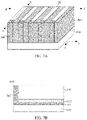
- FIG. 7B is a cross-sectional diagram along a cutting line A-A' in FIG. 7A
- FIG. 7C is a cross-sectional diagram along a cutting line B-B' in FIG. 7A .
- the conductive material such as polycrystalline silicon or a metal material, e.g., W, Co, Ag, or Al, can be formed in the gap 600 by a method such as atomic layer deposition, chemical vapor deposition, or physical vapor deposition.
- the conductive material can also be a multi-layer material such as a combination of TiN and W.
- the conductive material fills the gap 600 to form the bit line 701 located at the bottom of the active line 131.
- the conductive material further fills the opening 501 and covers tops of the first isolation layer 500 and the active line 131. Subsequently, the conductive material on the tops of the first isolation layer 500 and the active line 131 can be removed by etching back or planarization treatment.
- the opening 501 is filled with the conductive material, therefore a bit line connecting line 702 located inside the opening 501 is formed.
- the bit line connecting line 702 and the bit line 701 are formed in the same processing step, thereby saving process cost.
- a bottom of the bit line connecting line 702 is connected to the bit line 701 for leading out of the bit line 701 buried under the active line 131, thereby facilitating application of a control signal to the bit line 701.
- the bit line 701 is located under the active line 131, is in electric connection with the first doped region 1311 at the bottom of the active line 131, and extends along an extension direction of the active line 131.
- the active line 131 (refer to FIG. 7A ) is patterned to form a plurality of active columns 132 that are discrete.
- the active line 131 is patterned to form the active columns 132.
- the active columns 132 are arranged in array along a first direction (y-direction) and a second direction (x-direction).
- the first direction and the second direction form an angle of 90 degrees.
- the first direction and the second direction form an angle between 60 degrees to 90 degrees.
- the active column 132 After the active column 132 is formed, the active column can be subjected to ion implantation to form the channel region and the second doped region located above the channel region.
- the channel region is formed above the first doped region 1311 at the bottom of the active column 132 by means of ion implantation only.
- An internal doping concentration of the channel regions is adjusted through ion implantation, therefore a threshold voltage of the formed transistor is adjusted.
- P-type or N-type doping can be performed in the channel region. According to requirements of the threshold voltage, suitable doping types and doping concentrations can be selected. In other embodiments, doping to the channel region may not be necessary.
- a doped channel region can be formed in the active layer 130 by means of in-situ doping, the active layer 130 is then patterned to obtain the active column 132, and the doped channel layer is patterned into the channel region.
- the second doped region can be formed above the channel region through ion implantation.
- a second doped layer is formed at a corresponding position through in-situ doping, therefore after the active layer 130 is patterned to form the active column 132, the second doped layer is patterned into the second doped region.
- the active line may not be doped to form the first doped region 1311 in the foregoing step.
- the first doped region at the bottom of the active column 132 can be formed by means such as diffusion treatment of the doping transitional layer or ion implantation.
- the first isolation layer 500 is etched back to expose the active column 132 at a certain height.
- a first isolation layer 500a and an isolation dielectric layer 503 which are etched back are formed and have a height equivalent to that of the first doped region 1311.
- a surface of the first isolation layer 500a etched back is flush with and the top of the first doped region 1311.
- the surface of the first isolation layer 500a is slightly lower than or higher than a top boundary of the first doped region 1311, to expose an area, above the first doped region 1311, of the active column 132.
- first isolation layer 500 In the process that the first isolation layer 500 is etched back, a part of the first isolation layer 500, between the bit line 702 and the adjacent bit line connecting line 702 can be covered with a mask and prevented from being etched, therefore damage to the bit line connecting line 702 is avoided.
- the first isolation layer 500 at each position can be etched back.
- a gate dielectric layer and a gate electrode layer are sequentially formed on the first isolation layer 500a and the isolation dielectric layer 503 which are etched back, and on the exposed active column 132; and the gate dielectric layer and the gate electrode layer are patterned to form a gate structure 1000 surrounding the channel region of the active column and expose a top area of the active column 132.
- the gate dielectric layer can be a gate dielectric material such as silicon oxide, silicon oxynitride, hafnium oxide, or aluminum oxide; the gate electrode layer can be a conductive material such as polysilicon, tungsten, cobalt, or aluminum.
- the gate dielectric layer and the gate electrode layer sequentially covering the structure shown in FIG. 9 can be formed through a deposition process, and can be patterned through an etching process, therefore the gate structure 1000 is formed.
- the gate structure 1000 surrounds the channel region of the active column 132.
- the gate structure 1000 includes the gate dielectric layer and a gate electrode covering the gate dielectric layer.
- FIG. 10 only shows the gate electrode in the gate structure 1000.
- the gate electrodes of the gate structures 1000 on the active columns which are arranged in the same straight line along a second direction (x-direction) are mutually connected to form a word line.
- the gate structures 1000 on various active columns 132 may be independent to one another.
- an isolation dielectric layer 1001 fills between adjacent gate structures 1000 after the gate structures 1000 are formed.
- the top area of the active column 132 is subjected to ion implantation, to form the second doped region 1321.
- the second doped region 1321 and the first doped region 1311 are of the same doping type, and respectively serve as a source electrode or a drain electrode of a vertical transistor.
- the second doped region 1321 can also be formed by a suitable means such as in-situ doping, diffusion, or implantation in the foregoing step, which will not be elaborated here.
- FIG. 12B is a cross-sectional diagram along a cutting line A-A' in FIG. 12A
- FIG. 12C is a cross-sectional diagram of a cutting line B-B' in FIG. 12A .
- the second isolation layer 1200 can be made of an insulating dielectric material such as silicon oxide, and silicon oxynitride, and forms isolation layers, together with the first isolation layers 500 and 500a, and the isolation dielectric layer 503 and 1001, among the various vertical transistors, and provides a flat surface for forming of other semiconductor structures or material layers above the vertical transistor.
- an insulating dielectric material such as silicon oxide, and silicon oxynitride
- the vertical transistor is formed on the substrate, the buried bit line is formed between the position under the first doped region at the bottom of the vertical transistor, and the substrate, therefore area of the transistor can be reduced, and the problem that how to apply a control signal to the first doped region is solved.
- Embodiments of this application further provide a semiconductor structure.
- FIG. 12A to FIG. 12C are schematic structural diagrams of a semiconductor structure according to an embodiment of this application.
- the semiconductor structure includes: a substrate 110, a vertical transistor located on the substrate 110, and a bit line 701.
- the vertical transistor includes a first doped region 1311, a channel region 1322, a second doped region 132, and a gate structure 1000; the first doped region 1311, the channel region 1322, and the second doped region 1321 are sequentially upwards arranged on the substrate 110, and the gate structure 1000 surrounds the channel region 1322.
- the bit line 701 is connected to the first doped region 1311, and is located between a bottom of the first doped region 1311 and the substrate 110.
- a plurality of vertical transistors are formed on the semiconductor structure and arranged in array along a first direction (y-direction) and a second direction (x-direction).
- the first doped regions 1311 at bottoms of the vertical transistors arranged on the same straight line along the first direction are connected to the same bit line 701.
- the gate structures 1000 of the vertical transistors arranged on the same straight line along the second direction are connected mutually.
- the semiconductor further includes: isolation layers arranged among the various vertical transistors on the substrate 110.
- the isolation layers include a first isolation layer 500a located between adjacent bit lines 701 and adjacent first doped regions 1311; an isolation dielectric layer 503 located between adjacent first doped regions 1311 on the bit line 701; an isolation dielectric layer 1001 located between adjacent gate structures 1000 on the first isolation layer 500a and the isolation dielectric layer 503, and a second isolation layer 1200 located between adjacent second doped regions 1321 on the isolation dielectric layer 1001.
- the semiconductor structure further includes: an opening penetrating the active layer.
- a bit line connecting line 702 is formed in the opening.
- a bottom of the bit line connecting line 702 is connected to the bit line 701.
- the bit line connecting line 702 is located at one edge of the transistor array.
- One bit line connecting line 702 is formed at one side of each line of transistors arranged along the y-direction, which is connected to the bit line 701 arranged under the line of transistors.
- the openings are formed at the end portions of the same side of the various active lines, or the openings are formed at two ends of the active lines. Only one end portion of each active line is provided with the opening. The openings at the end portions on the same side are spaced apart to decrease a density of the openings formed on a local area and expand process windows.
- the first doped region 1311, the channel region 1322, and the second doped region 1321 of each vertical transistor are located in the same active column.
- the active column is of an integral structure.
- the first doped region 1311, the channel region 1322, and the second doped region 1321 are formed by doping.
- in the process of forming the active layer 130 in the process of forming the active layer 130 (refer to FIG.
- a first doped layer, a doped channel layer, and a second doped layer can be formed in the active layer 130 through in-situ doping; after the active layer 130 is patterned to form the active column 132, the first doped layer is patterned into the first doped region 1311, the doped channel layer is patterned into the channel region 1322, and the second doped layer is patterned into the second doped region 1321.
- the channel region 1322 and the second doped region 1321 of the vertical transistor are formed in an epitaxial semiconductor column on the first doped region 1311.
- a semiconductor layer where the channel region 1322 and the second doped region 1321 are located and the epitaxial semiconductor column are not an integral structure, but are separately formed.
- Doped ions in the first doped region 1311 and/or the second doped region 1321 are formed by means of diffusion or ion implantation.
- Embodiments of this application further provide a memory and a method for forming the same.
- FIG. 12A to FIG. 12C the semiconductor structure as shown in FIG. 12A to FIG. 12C is provided. Refer to the above-mentioned embodiments for a specific description of the semiconductor structure, which will not be elaborated here.
- a memory cell 1300 is formed on the vertical transistor, and is electrically connected to the second doped region 1321 of the vertical transistor.
- the memory refers to a DRAM.
- the memory cell 1300 refers to a capacitor including a top electrode, a bottom electrode, and a capacitor dielectric layer between the top electrode and the lower electrode.
- the capacitor can be of a structure such as a planar capacitor, and a cylindrical capacitor. Those skilled in the art may select the capacitor of the suitable structure as the memory cell according to needs. In FIG. 13 , the memory cell 1300 is only an example, which does not represent the actual structure of the capacitor.
- the second doped region 1321 of each transistor is connected to one memory cell to form a 1T1C storage structure.
- the memory cell can include a capacitor, or two or more capacitors connected in parallel.
- a metal contact layer can be formed on the second doped layer 1321, and the memory cell is formed on the metal contact layer.
- the memory cell 1300 is formed in a dielectric layer (not shown in the figure), alternatively, an interconnecting structure for connecting the bit line connecting line 702 and the gate structure 1000 can be formed in the dielectric layer, for connecting the bit line and word line to an external circuit.
- the memory cell can include any of various memory cells such as a capacitive memory cell, a magnetic memory cell, a ferroelectric memory cell, a phase change memory cell, or a resistive memory cell.
- FIG. 14 is a schematic structural diagram of a memory according to an embodiment of this application.
- the memory is a Ferroelectric Random Access Memory (FeRAM).
- FeRAM Ferroelectric Random Access Memory
- a ferroelectric memory cell 1400 in electric connection is formed on the second doped region 1321 of each vertical transistor of the semiconductor structure shown in FIG. 12A .
- the ferroelectric memory cell includes a bottom electrode connected to the second doped region 1321, a top electrode above the bottom electrode, and a ferroelectric capacitor, formed by a ferroelectric material layer, between the top electrode and the bottom electrode.
- the ferroelectric material layer can be made of a material of PZT (Pb-based lanthanum-doped zirconate titanates) or SBT (barium-strontium titanates).
- PZT Pb-based lanthanum-doped zirconate titanates
- SBT barium-strontium titanates
- a plate line 1401 connected to the top electrode is required to be formed on the ferroelectric memory cell 1400.
- the ferroelectric memory cells which are arranged on the same straight line along a second direction (x-direction) are connected to the same plate line 1401.
- a magnetic memory cell can also be formed on the second doped region 1321 of the vertical transistor.
- the magnetic memory cell includes a magnetic tunneling junction.
- the magnetic tunneling junction includes a fixed layer, a free layer, and a dielectric layer located between the fixed layer and the free layer.
- the fixed layer is connected to the second doped region 1321.
- a memory cell of other structures or types may be formed, so as to form a corresponding memory.
- the vertical transistor serving as a control transistor connected to the memory cell, and the buried bit line connected to the control transistor are used, which can increase a storage density of the memory.
Landscapes
- Engineering & Computer Science (AREA)
- Manufacturing & Machinery (AREA)
- Semiconductor Memories (AREA)
Abstract
Description
- The present application claims priority to
Chinese Patent Application No. 202010344169.4, filed on April 27, 2020 - This application relates to the technical field of semiconductors, in particular to, a semiconductor structure and a method for forming thereof, and a memory and a method for forming thereof.
- A memory usually includes a data memory cell and a control transistor for controlling the data memory cell. An integration density of the transistor restricts a storage density of the memory. For planar transistors, a channel size of the transistor is reduced to decrease a size of the transistor, thereby increasing the storage density of the memory.
- However, with a decrease of the channel size of the transistor, the narrow channel effect and the short channel effect lead to the degradation of transistor performance, which affects the performance of the memory and restricts the further improvement of the size of the transistor and the storage density of the memory.
- It is an urgent problem to be solved of how to decrease a planar size of the transistor and increase the storage density of the memory without reducing the performance of the transistor at present.
- The technical problem to be solved by this application is to provide a semiconductor structure and a method for forming thereof, and a memory and a method for forming thereof, further improving the storage density of a memory.
- In order to solve the above problem, this application provides a method for forming a semiconductor structure, including: providing a substrate, a sacrificial layer and an active layer on the sacrificial layer are formed on the substrate; etching the active layer and the sacrificial layer to form active lines extending along a first direction; forming a first isolation layer that fills spacing between the various active lines; etching ends of the active lines to form openings exposing the sacrificial layer; removing the sacrificial layer along the openings to form gaps between a bottom of the active lines and the substrate; and filling the gaps with a conductive material to form bit lines extending along the first direction.
- Optionally, the method further includes: filling the openings with a conductive material to form bit line connecting lines located in the openings, and a bottom of the bit line connecting lines being connected to the bit lines.
- Optionally, the method further includes: patterning the active lines to form a plurality of discrete active columns, the plurality of active columns being arranged in an array along the first direction and a second direction.
- Optionally, the method further includes: forming a first doped region, a channel region, and a second doped region located at a bottom of an active column and upwardly arranged in sequence, and forming a gate structure surrounding the channel region.
- Optionally, a method for forming the first doped region includes: performing ion implantation on the active column to form the first doped region located at the bottom of the active column.
- Optionally, a method for forming the first doped region includes: forming a transitional layer with doping elements between adjacent active lines or active columns on the substrate after the active lines or the active columns are formed; and through diffusion treatment, diffusing at least part of the doping elements in the transitional layer into the active line or the active column to form the first doped region.
- Optionally, a method for forming the first doped region, the channel region, and the second doped region includes: using an in-situ doping process, doping the active layer in the process of forming the active layer to sequentially form a first doped layer, a channel doped layer, and a second doped layer; after patterning the active layer to form the active columns, the first doped layer, the channel doped layer, and the second doped layer are respectively patterned to form the first doped region, the channel region, and the second doped region.
- Optionally, a method for forming the gate structure includes: etching back the first isolation layer to expose a part of the height of the active column; sequentially forming a gate dielectric layer and a gate electrode layer on the first isolation layer after being etched back and the exposed active column; and patterning the gate dielectric layer and the gate electrode layer to form the gate structure surrounding the channel region of the active column, and exposing a top area of the active column.
- Optionally, the gate structures on the active columns which are arranged on the same straight line along the second direction are mutually connected.
- Optionally, after the gate structure is formed, the top area of the active column is subjected to ion implantation to form the second doped region.
- Optionally, a second isolation layer covering the gate structure and the second doped region is formed, and the bit line connecting line and a top surface of the second doped region are exposed by the second isolation layer.
- Optionally, the bit line connecting line and the bit line are formed in the same processing step.
- Optionally, a plurality of openings are formed at two ends of the plurality of active lines and the openings correspond to the active lines one-to-one. The openings at the ends of the same side of the active lines are distributed at intervals. The technical solution of this application further provides a semiconductor structure formed by the foregoing method.
- The technical solution of this application further provides a memory, including the foregoing semiconductor structure, and a memory cell located above the semiconductor structure, and the memory cell electrically connected to the second doped region.
- Optionally, the memory cell includes any one of a capacitive memory cell, a magnetic memory cell, a ferroelectric memory cell, a phase change memory cell, or a resistive memory cell.
- The technical solution of this application further provides a method for forming a memory, including: providing the above-mentioned semiconductor structure; and forming a memory cell on the semiconductor structure, and the memory cell being electrically connected to the second doped region.
- Optionally, the memory cell includes any one of a capacitive memory cell, a magnetic memory cell, a ferroelectric memory cell, a phase change memory cell, or a resistive memory cell.
- In the method for forming a semiconductor structure in this application, the sacrificial layer and the active layer on the sacrificial layer are formed on the substrate; the position of the sacrificial layer is replaced with a bit line to form a buried bit line, thereby facilitating subsequent forming of a vertical transistor, and the source/drain at the bottom of the vertical transistor being led out through the bit line.
- Furthermore, the vertical transistor has a smaller layout size, and a channel length is determined by a thickness of the active layer, area of the transistor can be reduced without a decrease of the channel length etc., thereby improving the integration density of the semiconductor structure.
- The memory of this application includes a semiconductor structure having a vertical transistor array. The storage density of the memory can be increased in the case of a small size of the transistor.
- In order to describe the technical solutions of the embodiments in this application more clearly, the accompanying drawings required to be used in the embodiments of this application will be simply introduced below. It is apparent that the accompanying drawings in the following descriptions are only some embodiments of this application. Those of ordinary skill in the art may further obtain other accompanying drawings according to these accompanying drawings without creative work.
-
FIG. 1 to FIG. 12C are schematic structural diagrams of a process of forming a semiconductor structure according to an embodiment of this application. -
FIG. 13 is a schematic structural diagram of a memory according to an embodiment of this application. -
FIG. 14 is a schematic structural diagram of a memory according to an embodiment of this application. - In order to make the objectives, technical means, and effects thereof of this application clearer, this application will be described further below in conjunction with the accompany drawings. It is to be understood that the embodiments described here are only part of the embodiments of this application, not all of the embodiments, and not intended to limit this application All other embodiments obtained by those of ordinary skill in the art on the basis of the embodiments in this application without creative work shall fall within the scope of protection of this application.
- Refer to
FIG. 1 to FIG. 12C. FIG. 1 to FIG. 12C are schematic structural diagrams of a process of forming a semiconductor structure according to an embodiment of this application. - Referring to
FIG. 1 , asubstrate 110 is provided. Asacrificial layer 120 and anactive layer 130 on the sacrificial layer are formed on thesubstrate 110. - The
substrate 110 can be made of various semiconductor materials such as Si, Ge, or SiC, can be of a single-layer structure, and can also be of a compound structure, which is not limited herein. - The
sacrificial layer 120 and theactive layer 130 are sequentially formed on thesubstrate 110. Theactive layer 130 uses a semiconductor material such as Si, Ge, or Sic, and can use one or more of the semiconductor materials. Thesacrificial layer 120 is made of a material different from those of thesubstrate 110 and theactive layer 130, therefore influences to thesubstrate 110 and theactive layer 130 in a subsequent process of removing thesacrificial layer 120 can be reduced. - In the embodiment, the
substrate 110 is a silicon substrate, thesacrificial layer 120 is a SiGe layer, and the active layer is a silicon layer. After thesacrificial layer 120 is epitaxially formed on thesubstrate 110 by an epitaxial growth process, theactive layer 130 is then formed on thesacrificial layer 120 through the epitaxial process. - In fact, as long as the
sacrificial layer 120 is made of a different material from those of thesubstrate 110 and theactive layer 130, in the process of removing thesacrificial layer 120, thesacrificial layer 120 can achieve a high etch selectivity compared to thesubstrate 110 and theactive layer 130. - In some embodiments, the
substrate 110, thesacrificial layer 120, and theactive layer 130 each can be of a Silicon-On-Insulator (SOI) structure, and buried oxide in the SOI structure serves as thesacrificial layer 120. - In other embodiments, a bulk-silicon substrate may be subjected to ion implantation, therefore a doped layer is formed inside the bulk-silicon substrate to serve as the
sacrificial layer 120. For example, Ge is implanted into bulk-silicon; by controlling an implantation depth of Ge, a SiGe layer is formed inside the bulk-silicon to serve as thesacrificial layer 120, a silicon layer under the doped layer serves as thesubstrate 110, and a silicon layer on the doped layer serves as the active layer. In other embodiments, the doped layer can be formed by implantation of other elements, such as C, O, or N, and an etch rate of the doped layer is different from those of a material layer above and a material layer below, and thus thesacrificial layer 120 is formed. Preferably, thesacrificial layer 120 can be made of a material such as silicon oxide, silicon nitride, silicon oxynitride, or silicon oxycarbide. - The
active layer 130 is used for forming a vertical transistor, and thesacrificial layer 120 is used to be substituted to form a bit line in a subsequent process. According to a size of the vertical transistor to be formed and a size of the bit line, a thickness of thesacrificial layer 120 and a thickness of theactive layer 130 are reasonably set. In one embodiment, the thickness of the sacrificial layer can be 35 nm to 50 nm, and the thickness of theactive layer 130 can be 100 nm to 1000 nm. - Referring to
FIG. 2 , theactive layer 130 and thesacrificial layer 120 are etched to reach thesubstrate 110, therefore a plurality ofactive lines 131 that are arranged in parallel and extend long a first direction are formed. - In the embodiment, a method for forming the
active lines 131 further includes:
forming a patterning mask layer (not shown in the figure) on theactive layer 130, herein opening patterns extending along the first direction are provided in the patterning mask layer; with the patterning mask layer as a mask, etching theactive layer 130 and the sacrificial layer to form elongatedactive lines 131 and elongatedsacrificial layers 120a. - In the embodiment, the first direction refers to a y-direction. The
active layer 130 and thesacrificial layer 120 are etched by a dry etching process. In corresponding etching stages, corresponding etching gases are selected for etching theactive layer 130 and thesacrificial layer 120. - Referring to
FIG. 3 , atransitional layer 310 with doping elements is formed on thesubstrate 110 between adjacentactive lines 131. - The
transitional layer 310 with a certain thickness can be formed by etching back after deposition of a transitional layer material on the substrate 100. The thickness of thetransitional layer 130 can be adjusted according to dimensional requirements of a source/drain region of the transistor to be formed. - The
transitional layer 310 and theactive layer 131 are different in materials, which can be materials that facilitate diffusion of impurities, for example, polycrystalline silicon, and can also be other materials, for example, dielectric materials such as silicon oxide, silicon nitride, or silicon oxynitride. - A method for forming the
transitional layer 310 with doping elements includes:
after atransitional layer 310 with a certain thickness without being doped is formed on thesubstrate 110, performing ion implantation to achieve doping of thetransitional layer 310. Here, tops of theactive lines 131 are covered with the patterning mask layer. By controlling energy of ion implantation, only thetransitional layer 310 can be doped through ion implantation. Based on types of the transistor to be formed, N-type ions or P-type ions or atomic clusters with N-type ions or P-type ions can be implanted to thetransitional layer 310. The doping elements in thetransitional layer 310 can exist in the form of ions, atoms, compound molecules, or clusters. - In other embodiments, in a process of forming the
transitional layer 310, doping gases with doping elements can be added in deposition process gases through the in-situ doping process, therefore thetransitional layer 310 with doping elements is directly formed. - Referring to
FIG. 4 , by the diffusion treatment, at least part of the doping elements in the transitional layer 310 (refer toFIG. 3 ) with doping atoms are diffused into eachactive line 131 so as to form the firstdoped region 1311. - The diffusion treatment may refer to a thermal annealing process. Based on a diffusion rate of the doping atoms, an annealing process with appropriate parameters can be selected, and the doping elements in the
transitional layer 310 are diffused into theactive line 131 so as to form the firstdoped region 1311 with a thickness equivalent to that of thetransitional layer 310. - By adjusting concentrations of the doping elements in the
transitional layer 310, diffusion treatment time, temperature, etc., an internal doping concentration of the firstdoped region 1311 formed after the diffusion treatment can be adjusted. - In other embodiments, after the patterning mask layer on the top of the
active line 131 is removed, theactive line 131 is directly doped through ion implantation to form the firstdoped region 1311. Specifically, by controlling ion implanting energy and direction during the ion implantation and adjusting an implantation depth, the firstdoped region 1311 is formed at the bottom of theactive line 131. - In other embodiments, alternatively, the first doped region can be formed at the bottom of the active line or the active column by means of ion implantation in other subsequent steps, for example, after the active line is subsequently patterned to form the active column, or in other steps.
- In other embodiments, alternatively, the in-situ doping process can be adopted, in the process of forming the active layer through deposition by the epitaxy process, to dope the active layer to form the first doped region located at the bottom of the active layer. After the active layer is patterned, the first doped region located at the bottom of the active line is formed.
- Referring to
FIG. 5 , afirst isolation layer 500 filling the spacing between the variousactive lines 131 is formed on thesubstrate 110. An end of theactive line 131 is etched to form anopening 501, and thesacrificial layer 120a is exposed to a side wall of theopening 501. - The
first isolation layer 500 and thesacrificial layer 120a are made of different materials. Thefirst isolation layer 500 is made of an insulating material, and used for providing an electric isolation between theactive lines 131. In the embodiment, thefirst isolation layer 500 is made of a material of silicon oxide. In the embodiment, thefirst isolation layer 500 is formed by a chemical vapor deposition method. After an isolation material layer that fills the spacing between the adjacentactive lines 131 and covers the tops of theactive lines 131 is formed on thesubstrate 110, the isolation material layer is subjected to planarization to form thefirst isolation layer 500. In the embodiment, a top of thefirst isolation layer 500 is flush with the top of eachactive line 131. In other embodiments, a patterning mask layer used for patterning of the active layer is remained on the top of theactive line 131, and thefirst isolation layer 500 is flush with the patterning mask layer. In other embodiments, the patterning mask layer has been removed before forming of thefirst isolation layer 500, and thefirst isolation layer 500 still covers the top of the active line, which can protect the top of theactive line 131 in a subsequent process. - After the
isolation layer 500 is formed, one end of theactive line 131 is etched to form theopening 501. Theopening 501 exposes thesacrificial layer 120a. Specifically, a bottom of theopening 501 can expose the substrate 100, or can be located in thesacrificial layer 120a, as long as the bottom of theopening 501 at least exposes part of a side wall of thesacrificial layer 120a. - As shown in
FIG. 5 , a plurality ofopenings 501 can be formed at the end portions on the same side of the variousactive lines 131. In other embodiments, the plurality of openings are formed at two ends of the plurality of active lines, and are in one-to-one corresponding with the active lines, and the openings, at the end portions on the same side of the active lines are spaced apart, so as to decrease a density of the openings on a local area and expand process windows. - Referring to
FIG. 6 , thesacrificial layer 120a is removed along theopening 501, and agap 600 is formed between a bottom of theactive line 131 and thesubstrate 110. - The
sacrificial layer 120a is removed by a wet etching process. Those skilled in the art can select a suitable etching solution according to the material of thesacrificial layer 120a, to allow thesacrificial layer 120a to have a high etch selectivity compared with theactive line 131 and thefirst isolation layer 500 during the wet etching process, therefore influences to theactive line 131 and thefirst isolation layer 500 can be reduced in a process of removing thesacrificial layer 120a. - After the
sacrificial layer 120a is removed, theactive line 131 is supported by thefirst isolation layer 500, is suspended above thesubstrate 110, and forms thegap 600 with thesubstrate 110. - Referring to
FIG. 7A to FIG. 7C , thegap 600 is filled with a conductive material, therefore abit line 701 extending along a first direction is formed.FIG. 7B is a cross-sectional diagram along a cutting line A-A' inFIG. 7A , andFIG. 7C is a cross-sectional diagram along a cutting line B-B' inFIG. 7A . - The conductive material such as polycrystalline silicon or a metal material, e.g., W, Co, Ag, or Al, can be formed in the
gap 600 by a method such as atomic layer deposition, chemical vapor deposition, or physical vapor deposition. The conductive material can also be a multi-layer material such as a combination of TiN and W. - The conductive material fills the
gap 600 to form thebit line 701 located at the bottom of theactive line 131. The conductive material further fills theopening 501 and covers tops of thefirst isolation layer 500 and theactive line 131. Subsequently, the conductive material on the tops of thefirst isolation layer 500 and theactive line 131 can be removed by etching back or planarization treatment. Theopening 501 is filled with the conductive material, therefore a bitline connecting line 702 located inside theopening 501 is formed. The bitline connecting line 702 and thebit line 701 are formed in the same processing step, thereby saving process cost. A bottom of the bitline connecting line 702 is connected to thebit line 701 for leading out of thebit line 701 buried under theactive line 131, thereby facilitating application of a control signal to thebit line 701. Thebit line 701 is located under theactive line 131, is in electric connection with the firstdoped region 1311 at the bottom of theactive line 131, and extends along an extension direction of theactive line 131. - Referring to
FiG. 8 , the active line 131 (refer toFIG. 7A ) is patterned to form a plurality ofactive columns 132 that are discrete. - Through a selective etching process, the
active line 131 is patterned to form theactive columns 132. Theactive columns 132 are arranged in array along a first direction (y-direction) and a second direction (x-direction). In the embodiment, the first direction and the second direction form an angle of 90 degrees. In other embodiments, the first direction and the second direction form an angle between 60 degrees to 90 degrees. - After the
active column 132 is formed, the active column can be subjected to ion implantation to form the channel region and the second doped region located above the channel region. - In the embodiment, after the
active column 132 is formed, the channel region is formed above the firstdoped region 1311 at the bottom of theactive column 132 by means of ion implantation only. An internal doping concentration of the channel regions is adjusted through ion implantation, therefore a threshold voltage of the formed transistor is adjusted. P-type or N-type doping can be performed in the channel region. According to requirements of the threshold voltage, suitable doping types and doping concentrations can be selected. In other embodiments, doping to the channel region may not be necessary. - In other embodiments, in the foregoing process of forming the active layer 130 (refer to
FIG. 1 ), alternatively, a doped channel region can be formed in theactive layer 130 by means of in-situ doping, theactive layer 130 is then patterned to obtain theactive column 132, and the doped channel layer is patterned into the channel region. - In the embodiment of this application, alternatively, the second doped region can be formed above the channel region through ion implantation. Or in the process of forming the
active layer 130, a second doped layer is formed at a corresponding position through in-situ doping, therefore after theactive layer 130 is patterned to form theactive column 132, the second doped layer is patterned into the second doped region. - In other specific manners, alternatively, the active line may not be doped to form the first
doped region 1311 in the foregoing step. Instead, after theactive column 132 is formed in the step, the first doped region at the bottom of theactive column 132 can be formed by means such as diffusion treatment of the doping transitional layer or ion implantation. - Referring to
FIG. 9 , thefirst isolation layer 500 is etched back to expose theactive column 132 at a certain height. - Before the
first isolation layer 500 is etched back, an opening between adjacentactive columns 132 is filled with an isolation dielectric material, and thefirst isolation layer 500 and the isolation dielectric material are etched back simultaneously, therefore afirst isolation layer 500a and anisolation dielectric layer 503 which are etched back are formed and have a height equivalent to that of the firstdoped region 1311. In the embodiment, a surface of thefirst isolation layer 500a etched back is flush with and the top of the firstdoped region 1311. In other embodiments, the surface of thefirst isolation layer 500a is slightly lower than or higher than a top boundary of the firstdoped region 1311, to expose an area, above the firstdoped region 1311, of theactive column 132. - In the process that the
first isolation layer 500 is etched back, a part of thefirst isolation layer 500, between thebit line 702 and the adjacent bitline connecting line 702 can be covered with a mask and prevented from being etched, therefore damage to the bitline connecting line 702 is avoided. - In other embodiments, the
first isolation layer 500 at each position can be etched back. - Referring to
FIG. 10 , a gate dielectric layer and a gate electrode layer are sequentially formed on thefirst isolation layer 500a and theisolation dielectric layer 503 which are etched back, and on the exposedactive column 132; and the gate dielectric layer and the gate electrode layer are patterned to form agate structure 1000 surrounding the channel region of the active column and expose a top area of theactive column 132. - The gate dielectric layer can be a gate dielectric material such as silicon oxide, silicon oxynitride, hafnium oxide, or aluminum oxide; the gate electrode layer can be a conductive material such as polysilicon, tungsten, cobalt, or aluminum. The gate dielectric layer and the gate electrode layer sequentially covering the structure shown in
FIG. 9 can be formed through a deposition process, and can be patterned through an etching process, therefore thegate structure 1000 is formed. Thegate structure 1000 surrounds the channel region of theactive column 132. Thegate structure 1000 includes the gate dielectric layer and a gate electrode covering the gate dielectric layer.FIG. 10 only shows the gate electrode in thegate structure 1000. - In the embodiment, the gate electrodes of the
gate structures 1000 on the active columns which are arranged in the same straight line along a second direction (x-direction) are mutually connected to form a word line. - In other embodiments, the
gate structures 1000 on variousactive columns 132 may be independent to one another. - In order achieve the electric isolation between the
gate structures 1000, anisolation dielectric layer 1001 fills betweenadjacent gate structures 1000 after thegate structures 1000 are formed. - Referring to
FIG. 11 , after thegate structure 1000 is formed, the top area of theactive column 132 is subjected to ion implantation, to form the seconddoped region 1321. - The second
doped region 1321 and the firstdoped region 1311 are of the same doping type, and respectively serve as a source electrode or a drain electrode of a vertical transistor. In other embodiment, the seconddoped region 1321 can also be formed by a suitable means such as in-situ doping, diffusion, or implantation in the foregoing step, which will not be elaborated here. - Referring to
FIG. 12Ato FIG. 12C , asecond isolation layer 1200 covering thegate structure 1000 and the seconddoped region 1321 is formed, and top surfaces of the bitline connecting line 702 and the seconddoped region 1321 are exposed by thesecond isolation layer 1200.FIG. 12B is a cross-sectional diagram along a cutting line A-A' inFIG. 12A , andFIG. 12C is a cross-sectional diagram of a cutting line B-B' inFIG. 12A . - The
second isolation layer 1200 can be made of an insulating dielectric material such as silicon oxide, and silicon oxynitride, and forms isolation layers, together with the first isolation layers 500 and 500a, and theisolation dielectric layer - By the foregoing method, the vertical transistor is formed on the substrate, the buried bit line is formed between the position under the first doped region at the bottom of the vertical transistor, and the substrate, therefore area of the transistor can be reduced, and the problem that how to apply a control signal to the first doped region is solved.
- Embodiments of this application further provide a semiconductor structure.
- Refer to
FIG. 12A to FIG. 12C. FIG. 12A to FIG. 12C are schematic structural diagrams of a semiconductor structure according to an embodiment of this application. - The semiconductor structure includes: a
substrate 110, a vertical transistor located on thesubstrate 110, and abit line 701. The vertical transistor includes a firstdoped region 1311, achannel region 1322, a seconddoped region 132, and agate structure 1000; the firstdoped region 1311, thechannel region 1322, and the seconddoped region 1321 are sequentially upwards arranged on thesubstrate 110, and thegate structure 1000 surrounds thechannel region 1322. Thebit line 701 is connected to the firstdoped region 1311, and is located between a bottom of the firstdoped region 1311 and thesubstrate 110. - A plurality of vertical transistors are formed on the semiconductor structure and arranged in array along a first direction (y-direction) and a second direction (x-direction). The first
doped regions 1311 at bottoms of the vertical transistors arranged on the same straight line along the first direction are connected to thesame bit line 701. Thegate structures 1000 of the vertical transistors arranged on the same straight line along the second direction are connected mutually. - The semiconductor further includes: isolation layers arranged among the various vertical transistors on the
substrate 110. The isolation layers include afirst isolation layer 500a located betweenadjacent bit lines 701 and adjacent firstdoped regions 1311; anisolation dielectric layer 503 located between adjacent firstdoped regions 1311 on thebit line 701; anisolation dielectric layer 1001 located betweenadjacent gate structures 1000 on thefirst isolation layer 500a and theisolation dielectric layer 503, and asecond isolation layer 1200 located between adjacent seconddoped regions 1321 on theisolation dielectric layer 1001. - The semiconductor structure further includes: an opening penetrating the active layer. A bit
line connecting line 702 is formed in the opening. A bottom of the bitline connecting line 702 is connected to thebit line 701. In the embodiment, the bitline connecting line 702 is located at one edge of the transistor array. One bitline connecting line 702 is formed at one side of each line of transistors arranged along the y-direction, which is connected to thebit line 701 arranged under the line of transistors. Specifically, the openings are formed at the end portions of the same side of the various active lines, or the openings are formed at two ends of the active lines. Only one end portion of each active line is provided with the opening. The openings at the end portions on the same side are spaced apart to decrease a density of the openings formed on a local area and expand process windows. - In some embodiments, the first
doped region 1311, thechannel region 1322, and the seconddoped region 1321 of each vertical transistor are located in the same active column. The active column is of an integral structure. The firstdoped region 1311, thechannel region 1322, and the seconddoped region 1321 are formed by doping. In other embodiments, in the process of forming the active layer 130 (refer toFIG. 1 ), alternatively, a first doped layer, a doped channel layer, and a second doped layer can be formed in theactive layer 130 through in-situ doping; after theactive layer 130 is patterned to form theactive column 132, the first doped layer is patterned into the firstdoped region 1311, the doped channel layer is patterned into thechannel region 1322, and the second doped layer is patterned into the seconddoped region 1321. In other embodiments, thechannel region 1322 and the seconddoped region 1321 of the vertical transistor are formed in an epitaxial semiconductor column on the firstdoped region 1311. A semiconductor layer where thechannel region 1322 and the seconddoped region 1321 are located and the epitaxial semiconductor column are not an integral structure, but are separately formed. - Doped ions in the first
doped region 1311 and/or the seconddoped region 1321 are formed by means of diffusion or ion implantation. - Embodiments of this application further provide a memory and a method for forming the same.
- Firstly, the semiconductor structure as shown in
FIG. 12A to FIG. 12C is provided. Refer to the above-mentioned embodiments for a specific description of the semiconductor structure, which will not be elaborated here. - Referring to
FIG. 13 , amemory cell 1300 is formed on the vertical transistor, and is electrically connected to the seconddoped region 1321 of the vertical transistor. - In one embodiment, the memory refers to a DRAM. The
memory cell 1300 refers to a capacitor including a top electrode, a bottom electrode, and a capacitor dielectric layer between the top electrode and the lower electrode. The capacitor can be of a structure such as a planar capacitor, and a cylindrical capacitor. Those skilled in the art may select the capacitor of the suitable structure as the memory cell according to needs. InFIG. 13 , thememory cell 1300 is only an example, which does not represent the actual structure of the capacitor. In the embodiment, the seconddoped region 1321 of each transistor is connected to one memory cell to form a 1T1C storage structure. The memory cell can include a capacitor, or two or more capacitors connected in parallel. - In other embodiments, alternatively, in order to reduce a connection resistance between the second
doped region 1321 and thememory cell 1300, a metal contact layer can be formed on the second dopedlayer 1321, and the memory cell is formed on the metal contact layer. - The
memory cell 1300 is formed in a dielectric layer (not shown in the figure), alternatively, an interconnecting structure for connecting the bitline connecting line 702 and thegate structure 1000 can be formed in the dielectric layer, for connecting the bit line and word line to an external circuit. - In other embodiments of this application, alternatively, the memory cell can include any of various memory cells such as a capacitive memory cell, a magnetic memory cell, a ferroelectric memory cell, a phase change memory cell, or a resistive memory cell.
-
FIG. 14 is a schematic structural diagram of a memory according to an embodiment of this application. - The memory is a Ferroelectric Random Access Memory (FeRAM). A
ferroelectric memory cell 1400 in electric connection is formed on the seconddoped region 1321 of each vertical transistor of the semiconductor structure shown inFIG. 12A . - The ferroelectric memory cell includes a bottom electrode connected to the second
doped region 1321, a top electrode above the bottom electrode, and a ferroelectric capacitor, formed by a ferroelectric material layer, between the top electrode and the bottom electrode. The ferroelectric material layer can be made of a material of PZT (Pb-based lanthanum-doped zirconate titanates) or SBT (barium-strontium titanates). Theferroelectric memory cell 1400 inFIG. 14 is only an example, which does not represent the actual structure of the ferroelectric memory cell. Those skilled in the art should select theferroelectric memory cell 1400 of a corresponding structure according to needs, which is not limited herein. - For the
ferroelectric memory cell 1400, aplate line 1401 connected to the top electrode is required to be formed on theferroelectric memory cell 1400. In the embodiment, the ferroelectric memory cells which are arranged on the same straight line along a second direction (x-direction) are connected to thesame plate line 1401. By means of theplate line 1401 and the vertical transistor below, two-way pressurization to theferroelectric memory cell 1400 can be achieved, therefore data storage is carried out according to properties of the ferroelectric material layer. - In other embodiments, a magnetic memory cell can also be formed on the second
doped region 1321 of the vertical transistor. The magnetic memory cell includes a magnetic tunneling junction. The magnetic tunneling junction includes a fixed layer, a free layer, and a dielectric layer located between the fixed layer and the free layer. The fixed layer is connected to the seconddoped region 1321. - In other embodiments, alternatively, a memory cell of other structures or types may be formed, so as to form a corresponding memory.
- According to the memory and the method for forming a memory, the vertical transistor serving as a control transistor connected to the memory cell, and the buried bit line connected to the control transistor are used, which can increase a storage density of the memory.
- The above are merely the preferred implementation manners of this application. It should be pointed out that those of ordinary skill in the art may also make several improvements and modifications without departing from the principle of this application. These improvements and modifications shall fall within the scope of protection of this application.
Claims (17)
- A method for forming a semiconductor structure, comprising:providing a substrate, wherein a sacrificial layer and an active layer on the sacrificial layer are formed on the substrate;etching the active layer and the sacrificial layer to form active lines along a first direction;forming first isolation layers that fill spacing between the active lines;etching end portions of the active lines to form openings exposing the sacrificial layer;removing the sacrificial layer along the openings, and forming gaps between a bottom of the active lines and the substrate; andfilling the gaps with a conductive material to form bit lines extending along the first direction.
- The method for forming a semiconductor structure according to claim 1, further comprising: filling the openings with the conductive material to form bit line connecting lines located in the openings, wherein a bottom of the bit line connecting lines is connected to the bit lines.
- The method for forming a semiconductor structure according to claim 1, further comprising: patterning the active lines to form a plurality of active columns that are discrete, the plurality of active columns being arranged in an array along the first direction and a second direction.
- The method for forming a semiconductor structure according to claim 3, further comprising: forming a first doped region, a channel region, and a second doped region that are located on a bottom of an active column and sequentially arranged upwards, and forming a gate structure surrounding the channel region.
- The method for forming a semiconductor structure according to claim 4, wherein a method for forming the first doped region comprises: performing ion implantation to the active column to form the first doped region located at the bottom of the active column.
- The method for forming a semiconductor structure according to claim 4, wherein a method for forming the first doped region comprises: forming a transitional layer with doping elements on the substrate between adjacent active lines or active columns, after the active lines or active columns are formed; and through diffusion treatment, diffusing at least part of the doping elements in the transitional layer into the active line or the active column to form the first doped region.
- The method for forming a semiconductor structure according to claim 4, wherein a method for forming the first doped region, the channel region, and the second doped region comprises: using an in-situ doping process, in the process of forming the active layer, doping the active layer to sequentially form a first doped layer, a channel doped layer, and a second doped layer; and after patterning the active layer to form the active column, the first doped layer, the channel doped layer, and the second doped layer are respectively patterned into the first doped region, the channel region, and the second doped region.
- The method for forming a semiconductor structure according to claim 4, wherein a method for forming the gate structure comprises: etching back a first isolation layer to expose a part of the height of the active column; sequentially forming a gate dielectric layer and a gate electrode layer on the first isolation layer of having been etched back and on the exposed active column; and patterning the gate dielectric layer and the gate electrode layer to form the gate structure surrounding the channel region of the active column and expose a top area of the active column.
- The method for forming a semiconductor structure according to claim 8, wherein the gate structures on the plurality of active columns arranged on a same straight line along the second direction are connected.
- The method for forming a semiconductor structure according to claim 8, wherein after the gate structure is formed, ion implantation is performed on the top area of the active columns to form the second doped region.
- The method for forming a semiconductor structure according to claim 2, wherein the bit line connecting lines and the bit lines are formed in a same processing step.
- The method for forming a semiconductor structure according to claim 1, wherein a plurality of openings are formed at two ends of the plurality of active lines, and the plurality of openings correspond to the active lines on a one-to-one basis, and the openings at ends of a same side of the active lines are distributed at intervals.
- A semiconductor structure, formed by the method according to claim 1.
- A memory, comprising:the semiconductor structure formed by the method as claimed in claim 4; anda memory cell located over the semiconductor structure; the memory cell being electrically coupled to the second doped region.
- The memory according to claim 14, wherein the memory cell comprises any one of a capacitive memory cell, a magnetic memory cell, a ferroelectric memory cell, a phase change memory cell, or a resistive memory cell.
- A method for forming a memory, comprising:providing the semiconductor structure formed according to claim 4; andforming a memory cell on the semiconductor structure, the memory cell being electrically coupled to the second doped region.
- The method for forming a memory according to claim 16, wherein the memory cell comprises any one of a capacitive memory cell, a magnetic memory cell, a ferroelectric memory cell, a phase change memory cell, or a resistive memory cell.
Applications Claiming Priority (2)
| Application Number | Priority Date | Filing Date | Title |
|---|---|---|---|
| CN202010344169.4A CN113644066B (en) | 2020-04-27 | 2020-04-27 | Semiconductor structure and method of forming the same, memory and method of forming the same |
| PCT/CN2021/086466 WO2021218606A1 (en) | 2020-04-27 | 2021-04-12 | Semiconductor structure and forming method therefor, memory and forming method therefor |
Publications (3)
| Publication Number | Publication Date |
|---|---|
| EP3975251A1 true EP3975251A1 (en) | 2022-03-30 |
| EP3975251A4 EP3975251A4 (en) | 2022-10-19 |
| EP3975251B1 EP3975251B1 (en) | 2024-01-24 |
Family
ID=78373184
Family Applications (1)
| Application Number | Title | Priority Date | Filing Date |
|---|---|---|---|
| EP21797030.0A Active EP3975251B1 (en) | 2020-04-27 | 2021-04-12 | Method for forming a memory structure |
Country Status (4)
| Country | Link |
|---|---|
| US (1) | US12082419B2 (en) |
| EP (1) | EP3975251B1 (en) |
| CN (1) | CN113644066B (en) |
| WO (1) | WO2021218606A1 (en) |
Families Citing this family (15)
| Publication number | Priority date | Publication date | Assignee | Title |
|---|---|---|---|---|
| CN113644065B (en) * | 2020-04-27 | 2024-03-29 | 长鑫存储技术有限公司 | Semiconductor structure and forming method thereof, memory and forming method thereof |
| CN116801611A (en) | 2022-03-15 | 2023-09-22 | 长鑫存储技术有限公司 | Memory, semiconductor structure and preparation method thereof |
| CN117042440A (en) * | 2022-04-29 | 2023-11-10 | 长鑫存储技术有限公司 | Semiconductor structures and preparation methods |
| CN115188737A (en) * | 2022-06-02 | 2022-10-14 | 长鑫存储技术有限公司 | Semiconductor structure and preparation method thereof |
| US12300744B2 (en) | 2022-06-02 | 2025-05-13 | Changxin Memory Technologies, Inc. | Semiconductor structure and manufacturing method thereof |
| CN115064540A (en) * | 2022-06-16 | 2022-09-16 | 长鑫存储技术有限公司 | Semiconductor structure, memory structure and preparation method thereof |
| CN117334567A (en) * | 2022-06-24 | 2024-01-02 | 长鑫存储技术有限公司 | Semiconductor structure and formation method, layout structure |
| EP4318586B1 (en) | 2022-06-24 | 2025-12-10 | Changxin Memory Technologies, Inc. | Semiconductor structure and forming method therefor, and layout structure |
| EP4329455A4 (en) | 2022-06-24 | 2024-09-04 | Changxin Memory Technologies, Inc. | SEMICONDUCTOR STRUCTURE AND FORMING METHOD THEREOF, AND ARRANGEMENT STRUCTURE |
| CN117334566A (en) | 2022-06-24 | 2024-01-02 | 长鑫存储技术有限公司 | Semiconductor structure and formation method, layout structure |
| CN117423654A (en) * | 2022-07-05 | 2024-01-19 | 长鑫存储技术有限公司 | Semiconductor structure manufacturing method and semiconductor structure |
| CN116033747B (en) * | 2023-01-05 | 2025-05-30 | 长鑫存储技术有限公司 | Semiconductor structure and forming method thereof |
| CN118969614B (en) * | 2023-05-08 | 2025-10-17 | 长鑫存储技术有限公司 | Semiconductor structure and preparation method thereof |
| CN119136532B (en) * | 2023-06-05 | 2025-09-26 | 长鑫存储技术有限公司 | semiconductor structure |
| CN117715440A (en) * | 2023-11-22 | 2024-03-15 | 厦门半导体工业技术研发有限公司 | Semiconductor structure and preparation method thereof |
Family Cites Families (14)
| Publication number | Priority date | Publication date | Assignee | Title |
|---|---|---|---|---|
| KR100699839B1 (en) * | 2005-04-21 | 2007-03-27 | 삼성전자주식회사 | A semiconductor device having multiple channels and a method of manufacturing the same. |
| KR101129030B1 (en) * | 2010-07-09 | 2012-03-23 | 주식회사 하이닉스반도체 | Method for forming etching barrier by using shadow effect and method for fabricating one side contact of vertical transistor |
| KR101154006B1 (en) | 2010-11-08 | 2012-06-07 | 에스케이하이닉스 주식회사 | Vertical transistor having buried junction and manufacturing method for the same |
| JP2013098295A (en) * | 2011-10-31 | 2013-05-20 | Elpida Memory Inc | Semiconductor device, manufacturing method of the same and data processing system |
| KR20130075348A (en) * | 2011-12-27 | 2013-07-05 | 에스케이하이닉스 주식회사 | Semiconductor device having buried bitline and fabricating the same |
| KR102008422B1 (en) * | 2012-12-17 | 2019-08-08 | 에스케이하이닉스 주식회사 | Nonvolatile memory device and method for fabricating the same |
| CN105448840B (en) * | 2014-08-28 | 2019-01-22 | 中芯国际集成电路制造(上海)有限公司 | The forming method of semiconductor structure |
| US11289490B2 (en) | 2017-03-31 | 2022-03-29 | Intel Corporation | Vertical 1T-1C DRAM array |
| CN109461756B (en) * | 2017-09-06 | 2021-05-14 | 中国科学院微电子研究所 | MRAM, manufacturing method thereof, and electronic device including MRAM |
| CN109461738B (en) | 2017-09-06 | 2021-03-26 | 中国科学院微电子研究所 | Semiconductor memory device, method of manufacturing the same, and electronic device including the same |
| CN108461496B (en) * | 2018-05-09 | 2023-09-29 | 长鑫存储技术有限公司 | Integrated circuit memory and formation method thereof, semiconductor integrated circuit device |
| CN110767549B (en) * | 2018-07-26 | 2023-05-16 | 中芯国际集成电路制造(北京)有限公司 | Semiconductor structure and forming method thereof |
| CN109285836B (en) * | 2018-08-28 | 2023-10-10 | 中国科学院微电子研究所 | Semiconductor storage device, manufacturing method thereof, and electronic device including storage device |
| CN211719592U (en) * | 2020-04-27 | 2020-10-20 | 长鑫存储技术有限公司 | Semiconductor structures and memories |
-
2020
- 2020-04-27 CN CN202010344169.4A patent/CN113644066B/en active Active
-
2021
- 2021-04-12 EP EP21797030.0A patent/EP3975251B1/en active Active
- 2021-04-12 WO PCT/CN2021/086466 patent/WO2021218606A1/en not_active Ceased
- 2021-08-10 US US17/444,785 patent/US12082419B2/en active Active
Also Published As
| Publication number | Publication date |
|---|---|
| US12082419B2 (en) | 2024-09-03 |
| EP3975251A4 (en) | 2022-10-19 |
| CN113644066B (en) | 2023-09-29 |
| US20210375939A1 (en) | 2021-12-02 |
| WO2021218606A1 (en) | 2021-11-04 |
| CN113644066A (en) | 2021-11-12 |
| EP3975251B1 (en) | 2024-01-24 |
Similar Documents
| Publication | Publication Date | Title |
|---|---|---|
| EP3975251B1 (en) | Method for forming a memory structure | |
| EP3933922B1 (en) | Semiconductor structure, forming method therefor and memory | |
| CN211719592U (en) | Semiconductor structures and memories | |
| EP3933921B1 (en) | Semiconductor structure, method for forming same, and memory | |
| US12101927B2 (en) | Semiconductor structure and method of forming the same, memory and method of forming the same | |
| US12340870B2 (en) | Method for forming a semiconductor device pillar with source, channel, and drain | |
| US12075612B2 (en) | Semiconductor structure and method for forming the same, and memory and method for forming the same | |
| US9391092B2 (en) | Circuit structures, memory circuitry, and methods | |
| US12598791B2 (en) | Storage device, method for manufacturing the same, and electronic apparatus including storage device | |
| US12597460B2 (en) | Storage device, method for manufacturing the same, and electronic device including storage device | |
| US20240081052A1 (en) | Memory Arrays Comprising Strings Of Memory Cells And Methods Used In Forming A Memory Array Comprising Strings Of Memory Cells | |
| US12058861B2 (en) | Memory arrays comprising strings of memory cells and methods used in forming a memory array comprising strings of memory cells |
Legal Events
| Date | Code | Title | Description |
|---|---|---|---|
| STAA | Information on the status of an ep patent application or granted ep patent |
Free format text: STATUS: THE INTERNATIONAL PUBLICATION HAS BEEN MADE |
|
| PUAI | Public reference made under article 153(3) epc to a published international application that has entered the european phase |
Free format text: ORIGINAL CODE: 0009012 |
|
| STAA | Information on the status of an ep patent application or granted ep patent |
Free format text: STATUS: REQUEST FOR EXAMINATION WAS MADE |
|
| 17P | Request for examination filed |
Effective date: 20211220 |
|
| AK | Designated contracting states |
Kind code of ref document: A1 Designated state(s): AL AT BE BG CH CY CZ DE DK EE ES FI FR GB GR HR HU IE IS IT LI LT LU LV MC MK MT NL NO PL PT RO RS SE SI SK SM TR |
|
| A4 | Supplementary search report drawn up and despatched |
Effective date: 20220915 |
|
| RIC1 | Information provided on ipc code assigned before grant |
Ipc: H01L 21/8242 20060101ALI20220909BHEP Ipc: H01L 27/24 20060101ALI20220909BHEP Ipc: H01L 27/22 20060101ALI20220909BHEP Ipc: H01L 27/11507 20170101ALI20220909BHEP Ipc: H01L 27/108 20060101ALI20220909BHEP Ipc: H01L 21/8234 20060101ALI20220909BHEP Ipc: H01L 27/088 20060101AFI20220909BHEP |
|
| STAA | Information on the status of an ep patent application or granted ep patent |
Free format text: STATUS: EXAMINATION IS IN PROGRESS |
|
| 17Q | First examination report despatched |
Effective date: 20230315 |
|
| DAV | Request for validation of the european patent (deleted) | ||
| DAX | Request for extension of the european patent (deleted) | ||
| REG | Reference to a national code |
Ref country code: DE Ref legal event code: R079 Free format text: PREVIOUS MAIN CLASS: H01L0027088000 Ipc: H01L0029786000 Ref document number: 602021008797 Country of ref document: DE |
|
| RIC1 | Information provided on ipc code assigned before grant |
Ipc: H10B 63/00 20230101ALI20230803BHEP Ipc: H10B 61/00 20230101ALI20230803BHEP Ipc: H10B 53/30 20230101ALI20230803BHEP Ipc: H10B 12/00 20230101ALI20230803BHEP Ipc: H01L 29/786 20060101AFI20230803BHEP |
|
| GRAP | Despatch of communication of intention to grant a patent |
Free format text: ORIGINAL CODE: EPIDOSNIGR1 |
|
| STAA | Information on the status of an ep patent application or granted ep patent |
Free format text: STATUS: GRANT OF PATENT IS INTENDED |
|
| INTG | Intention to grant announced |
Effective date: 20230912 |
|
| P01 | Opt-out of the competence of the unified patent court (upc) registered |
Effective date: 20231018 |
|
| GRAS | Grant fee paid |
Free format text: ORIGINAL CODE: EPIDOSNIGR3 |
|
| GRAA | (expected) grant |
Free format text: ORIGINAL CODE: 0009210 |
|
| STAA | Information on the status of an ep patent application or granted ep patent |
Free format text: STATUS: THE PATENT HAS BEEN GRANTED |
|
| AK | Designated contracting states |
Kind code of ref document: B1 Designated state(s): AL AT BE BG CH CY CZ DE DK EE ES FI FR GB GR HR HU IE IS IT LI LT LU LV MC MK MT NL NO PL PT RO RS SE SI SK SM TR |
|
| REG | Reference to a national code |
Ref country code: GB Ref legal event code: FG4D |
|
| REG | Reference to a national code |
Ref country code: CH Ref legal event code: EP |
|
| REG | Reference to a national code |
Ref country code: DE Ref legal event code: R096 Ref document number: 602021008797 Country of ref document: DE |
|
| REG | Reference to a national code |
Ref country code: IE Ref legal event code: FG4D |
|
| REG | Reference to a national code |
Ref country code: LT Ref legal event code: MG9D |
|
| REG | Reference to a national code |
Ref country code: NL Ref legal event code: MP Effective date: 20240124 |
|
| PG25 | Lapsed in a contracting state [announced via postgrant information from national office to epo] |
Ref country code: NL Free format text: LAPSE BECAUSE OF FAILURE TO SUBMIT A TRANSLATION OF THE DESCRIPTION OR TO PAY THE FEE WITHIN THE PRESCRIBED TIME-LIMIT Effective date: 20240124 |
|
| PG25 | Lapsed in a contracting state [announced via postgrant information from national office to epo] |
Ref country code: NL Free format text: LAPSE BECAUSE OF FAILURE TO SUBMIT A TRANSLATION OF THE DESCRIPTION OR TO PAY THE FEE WITHIN THE PRESCRIBED TIME-LIMIT Effective date: 20240124 |
|
| PG25 | Lapsed in a contracting state [announced via postgrant information from national office to epo] |
Ref country code: IS Free format text: LAPSE BECAUSE OF FAILURE TO SUBMIT A TRANSLATION OF THE DESCRIPTION OR TO PAY THE FEE WITHIN THE PRESCRIBED TIME-LIMIT Effective date: 20240524 |
|
| PG25 | Lapsed in a contracting state [announced via postgrant information from national office to epo] |
Ref country code: LT Free format text: LAPSE BECAUSE OF FAILURE TO SUBMIT A TRANSLATION OF THE DESCRIPTION OR TO PAY THE FEE WITHIN THE PRESCRIBED TIME-LIMIT Effective date: 20240124 |
|
| PG25 | Lapsed in a contracting state [announced via postgrant information from national office to epo] |
Ref country code: GR Free format text: LAPSE BECAUSE OF FAILURE TO SUBMIT A TRANSLATION OF THE DESCRIPTION OR TO PAY THE FEE WITHIN THE PRESCRIBED TIME-LIMIT Effective date: 20240425 |
|
| REG | Reference to a national code |
Ref country code: AT Ref legal event code: MK05 Ref document number: 1652878 Country of ref document: AT Kind code of ref document: T Effective date: 20240124 |
|
| PG25 | Lapsed in a contracting state [announced via postgrant information from national office to epo] |
Ref country code: HR Free format text: LAPSE BECAUSE OF FAILURE TO SUBMIT A TRANSLATION OF THE DESCRIPTION OR TO PAY THE FEE WITHIN THE PRESCRIBED TIME-LIMIT Effective date: 20240124 Ref country code: RS Free format text: LAPSE BECAUSE OF FAILURE TO SUBMIT A TRANSLATION OF THE DESCRIPTION OR TO PAY THE FEE WITHIN THE PRESCRIBED TIME-LIMIT Effective date: 20240424 |
|
| PG25 | Lapsed in a contracting state [announced via postgrant information from national office to epo] |
Ref country code: ES Free format text: LAPSE BECAUSE OF FAILURE TO SUBMIT A TRANSLATION OF THE DESCRIPTION OR TO PAY THE FEE WITHIN THE PRESCRIBED TIME-LIMIT Effective date: 20240124 |
|
| PG25 | Lapsed in a contracting state [announced via postgrant information from national office to epo] |
Ref country code: AT Free format text: LAPSE BECAUSE OF FAILURE TO SUBMIT A TRANSLATION OF THE DESCRIPTION OR TO PAY THE FEE WITHIN THE PRESCRIBED TIME-LIMIT Effective date: 20240124 |
|
| PG25 | Lapsed in a contracting state [announced via postgrant information from national office to epo] |
Ref country code: RS Free format text: LAPSE BECAUSE OF FAILURE TO SUBMIT A TRANSLATION OF THE DESCRIPTION OR TO PAY THE FEE WITHIN THE PRESCRIBED TIME-LIMIT Effective date: 20240424 Ref country code: NO Free format text: LAPSE BECAUSE OF FAILURE TO SUBMIT A TRANSLATION OF THE DESCRIPTION OR TO PAY THE FEE WITHIN THE PRESCRIBED TIME-LIMIT Effective date: 20240424 Ref country code: LT Free format text: LAPSE BECAUSE OF FAILURE TO SUBMIT A TRANSLATION OF THE DESCRIPTION OR TO PAY THE FEE WITHIN THE PRESCRIBED TIME-LIMIT Effective date: 20240124 Ref country code: IS Free format text: LAPSE BECAUSE OF FAILURE TO SUBMIT A TRANSLATION OF THE DESCRIPTION OR TO PAY THE FEE WITHIN THE PRESCRIBED TIME-LIMIT Effective date: 20240524 Ref country code: HR Free format text: LAPSE BECAUSE OF FAILURE TO SUBMIT A TRANSLATION OF THE DESCRIPTION OR TO PAY THE FEE WITHIN THE PRESCRIBED TIME-LIMIT Effective date: 20240124 Ref country code: GR Free format text: LAPSE BECAUSE OF FAILURE TO SUBMIT A TRANSLATION OF THE DESCRIPTION OR TO PAY THE FEE WITHIN THE PRESCRIBED TIME-LIMIT Effective date: 20240425 Ref country code: FI Free format text: LAPSE BECAUSE OF FAILURE TO SUBMIT A TRANSLATION OF THE DESCRIPTION OR TO PAY THE FEE WITHIN THE PRESCRIBED TIME-LIMIT Effective date: 20240124 Ref country code: ES Free format text: LAPSE BECAUSE OF FAILURE TO SUBMIT A TRANSLATION OF THE DESCRIPTION OR TO PAY THE FEE WITHIN THE PRESCRIBED TIME-LIMIT Effective date: 20240124 Ref country code: BG Free format text: LAPSE BECAUSE OF FAILURE TO SUBMIT A TRANSLATION OF THE DESCRIPTION OR TO PAY THE FEE WITHIN THE PRESCRIBED TIME-LIMIT Effective date: 20240124 Ref country code: AT Free format text: LAPSE BECAUSE OF FAILURE TO SUBMIT A TRANSLATION OF THE DESCRIPTION OR TO PAY THE FEE WITHIN THE PRESCRIBED TIME-LIMIT Effective date: 20240124 |
|
| PG25 | Lapsed in a contracting state [announced via postgrant information from national office to epo] |
Ref country code: PT Free format text: LAPSE BECAUSE OF FAILURE TO SUBMIT A TRANSLATION OF THE DESCRIPTION OR TO PAY THE FEE WITHIN THE PRESCRIBED TIME-LIMIT Effective date: 20240524 Ref country code: PL Free format text: LAPSE BECAUSE OF FAILURE TO SUBMIT A TRANSLATION OF THE DESCRIPTION OR TO PAY THE FEE WITHIN THE PRESCRIBED TIME-LIMIT Effective date: 20240124 |
|
| PG25 | Lapsed in a contracting state [announced via postgrant information from national office to epo] |
Ref country code: SE Free format text: LAPSE BECAUSE OF FAILURE TO SUBMIT A TRANSLATION OF THE DESCRIPTION OR TO PAY THE FEE WITHIN THE PRESCRIBED TIME-LIMIT Effective date: 20240124 Ref country code: PT Free format text: LAPSE BECAUSE OF FAILURE TO SUBMIT A TRANSLATION OF THE DESCRIPTION OR TO PAY THE FEE WITHIN THE PRESCRIBED TIME-LIMIT Effective date: 20240524 Ref country code: PL Free format text: LAPSE BECAUSE OF FAILURE TO SUBMIT A TRANSLATION OF THE DESCRIPTION OR TO PAY THE FEE WITHIN THE PRESCRIBED TIME-LIMIT Effective date: 20240124 Ref country code: LV Free format text: LAPSE BECAUSE OF FAILURE TO SUBMIT A TRANSLATION OF THE DESCRIPTION OR TO PAY THE FEE WITHIN THE PRESCRIBED TIME-LIMIT Effective date: 20240124 |
|
| PG25 | Lapsed in a contracting state [announced via postgrant information from national office to epo] |
Ref country code: DK Free format text: LAPSE BECAUSE OF FAILURE TO SUBMIT A TRANSLATION OF THE DESCRIPTION OR TO PAY THE FEE WITHIN THE PRESCRIBED TIME-LIMIT Effective date: 20240124 |
|
| PG25 | Lapsed in a contracting state [announced via postgrant information from national office to epo] |
Ref country code: SM Free format text: LAPSE BECAUSE OF FAILURE TO SUBMIT A TRANSLATION OF THE DESCRIPTION OR TO PAY THE FEE WITHIN THE PRESCRIBED TIME-LIMIT Effective date: 20240124 |
|
| PG25 | Lapsed in a contracting state [announced via postgrant information from national office to epo] |
Ref country code: CZ Free format text: LAPSE BECAUSE OF FAILURE TO SUBMIT A TRANSLATION OF THE DESCRIPTION OR TO PAY THE FEE WITHIN THE PRESCRIBED TIME-LIMIT Effective date: 20240124 Ref country code: EE Free format text: LAPSE BECAUSE OF FAILURE TO SUBMIT A TRANSLATION OF THE DESCRIPTION OR TO PAY THE FEE WITHIN THE PRESCRIBED TIME-LIMIT Effective date: 20240124 |
|
| REG | Reference to a national code |
Ref country code: DE Ref legal event code: R097 Ref document number: 602021008797 Country of ref document: DE |
|
| PG25 | Lapsed in a contracting state [announced via postgrant information from national office to epo] |
Ref country code: SK Free format text: LAPSE BECAUSE OF FAILURE TO SUBMIT A TRANSLATION OF THE DESCRIPTION OR TO PAY THE FEE WITHIN THE PRESCRIBED TIME-LIMIT Effective date: 20240124 |
|
| PG25 | Lapsed in a contracting state [announced via postgrant information from national office to epo] |
Ref country code: SM Free format text: LAPSE BECAUSE OF FAILURE TO SUBMIT A TRANSLATION OF THE DESCRIPTION OR TO PAY THE FEE WITHIN THE PRESCRIBED TIME-LIMIT Effective date: 20240124 Ref country code: SK Free format text: LAPSE BECAUSE OF FAILURE TO SUBMIT A TRANSLATION OF THE DESCRIPTION OR TO PAY THE FEE WITHIN THE PRESCRIBED TIME-LIMIT Effective date: 20240124 Ref country code: EE Free format text: LAPSE BECAUSE OF FAILURE TO SUBMIT A TRANSLATION OF THE DESCRIPTION OR TO PAY THE FEE WITHIN THE PRESCRIBED TIME-LIMIT Effective date: 20240124 Ref country code: DK Free format text: LAPSE BECAUSE OF FAILURE TO SUBMIT A TRANSLATION OF THE DESCRIPTION OR TO PAY THE FEE WITHIN THE PRESCRIBED TIME-LIMIT Effective date: 20240124 Ref country code: CZ Free format text: LAPSE BECAUSE OF FAILURE TO SUBMIT A TRANSLATION OF THE DESCRIPTION OR TO PAY THE FEE WITHIN THE PRESCRIBED TIME-LIMIT Effective date: 20240124 |
|
| PG25 | Lapsed in a contracting state [announced via postgrant information from national office to epo] |
Ref country code: MC Free format text: LAPSE BECAUSE OF FAILURE TO SUBMIT A TRANSLATION OF THE DESCRIPTION OR TO PAY THE FEE WITHIN THE PRESCRIBED TIME-LIMIT Effective date: 20240124 |
|
| REG | Reference to a national code |
Ref country code: DE Ref legal event code: R079 Ref document number: 602021008797 Country of ref document: DE Free format text: PREVIOUS MAIN CLASS: H01L0029786000 Ipc: H10D0030670000 |
|
| PG25 | Lapsed in a contracting state [announced via postgrant information from national office to epo] |
Ref country code: MC Free format text: LAPSE BECAUSE OF FAILURE TO SUBMIT A TRANSLATION OF THE DESCRIPTION OR TO PAY THE FEE WITHIN THE PRESCRIBED TIME-LIMIT Effective date: 20240124 |
|
| PLBE | No opposition filed within time limit |
Free format text: ORIGINAL CODE: 0009261 |
|
| REG | Reference to a national code |
Ref country code: CH Ref legal event code: PL |
|
| STAA | Information on the status of an ep patent application or granted ep patent |
Free format text: STATUS: NO OPPOSITION FILED WITHIN TIME LIMIT |
|
| PG25 | Lapsed in a contracting state [announced via postgrant information from national office to epo] |
Ref country code: IT Free format text: LAPSE BECAUSE OF FAILURE TO SUBMIT A TRANSLATION OF THE DESCRIPTION OR TO PAY THE FEE WITHIN THE PRESCRIBED TIME-LIMIT Effective date: 20240124 |
|
| PG25 | Lapsed in a contracting state [announced via postgrant information from national office to epo] |
Ref country code: LU Free format text: LAPSE BECAUSE OF NON-PAYMENT OF DUE FEES Effective date: 20240412 |
|
| REG | Reference to a national code |
Ref country code: BE Ref legal event code: MM Effective date: 20240430 |
|
| PG25 | Lapsed in a contracting state [announced via postgrant information from national office to epo] |
Ref country code: LU Free format text: LAPSE BECAUSE OF NON-PAYMENT OF DUE FEES Effective date: 20240412 Ref country code: IT Free format text: LAPSE BECAUSE OF FAILURE TO SUBMIT A TRANSLATION OF THE DESCRIPTION OR TO PAY THE FEE WITHIN THE PRESCRIBED TIME-LIMIT Effective date: 20240124 |
|
| 26N | No opposition filed |
Effective date: 20241025 |
|
| PG25 | Lapsed in a contracting state [announced via postgrant information from national office to epo] |
Ref country code: BE Free format text: LAPSE BECAUSE OF NON-PAYMENT OF DUE FEES Effective date: 20240430 |
|
| PG25 | Lapsed in a contracting state [announced via postgrant information from national office to epo] |
Ref country code: FR Free format text: LAPSE BECAUSE OF NON-PAYMENT OF DUE FEES Effective date: 20240430 |
|
| PG25 | Lapsed in a contracting state [announced via postgrant information from national office to epo] |
Ref country code: FR Free format text: LAPSE BECAUSE OF NON-PAYMENT OF DUE FEES Effective date: 20240430 Ref country code: BE Free format text: LAPSE BECAUSE OF NON-PAYMENT OF DUE FEES Effective date: 20240430 Ref country code: CH Free format text: LAPSE BECAUSE OF NON-PAYMENT OF DUE FEES Effective date: 20240430 |
|
| PG25 | Lapsed in a contracting state [announced via postgrant information from national office to epo] |
Ref country code: IE Free format text: LAPSE BECAUSE OF NON-PAYMENT OF DUE FEES Effective date: 20240412 |
|
| PG25 | Lapsed in a contracting state [announced via postgrant information from national office to epo] |
Ref country code: SI Free format text: LAPSE BECAUSE OF FAILURE TO SUBMIT A TRANSLATION OF THE DESCRIPTION OR TO PAY THE FEE WITHIN THE PRESCRIBED TIME-LIMIT Effective date: 20240124 |
|
| PGFP | Annual fee paid to national office [announced via postgrant information from national office to epo] |
Ref country code: DE Payment date: 20250422 Year of fee payment: 5 |
|
| PG25 | Lapsed in a contracting state [announced via postgrant information from national office to epo] |
Ref country code: RO Free format text: LAPSE BECAUSE OF FAILURE TO SUBMIT A TRANSLATION OF THE DESCRIPTION OR TO PAY THE FEE WITHIN THE PRESCRIBED TIME-LIMIT Effective date: 20240124 |
|
| PG25 | Lapsed in a contracting state [announced via postgrant information from national office to epo] |
Ref country code: CY Free format text: LAPSE BECAUSE OF FAILURE TO SUBMIT A TRANSLATION OF THE DESCRIPTION OR TO PAY THE FEE WITHIN THE PRESCRIBED TIME-LIMIT; INVALID AB INITIO Effective date: 20210412 |
|
| PG25 | Lapsed in a contracting state [announced via postgrant information from national office to epo] |
Ref country code: HU Free format text: LAPSE BECAUSE OF FAILURE TO SUBMIT A TRANSLATION OF THE DESCRIPTION OR TO PAY THE FEE WITHIN THE PRESCRIBED TIME-LIMIT; INVALID AB INITIO Effective date: 20210412 |
|
| PGFP | Annual fee paid to national office [announced via postgrant information from national office to epo] |
Ref country code: GB Payment date: 20260306 Year of fee payment: 6 |