EP3974889A1 - Integrated electronic module including two micromirrors, and system including the electronic module - Google Patents
Integrated electronic module including two micromirrors, and system including the electronic module Download PDFInfo
- Publication number
- EP3974889A1 EP3974889A1 EP21198930.6A EP21198930A EP3974889A1 EP 3974889 A1 EP3974889 A1 EP 3974889A1 EP 21198930 A EP21198930 A EP 21198930A EP 3974889 A1 EP3974889 A1 EP 3974889A1
- Authority
- EP
- European Patent Office
- Prior art keywords
- electronic module
- reflector
- electrical
- module according
- supporting
- Prior art date
- Legal status (The legal status is an assumption and is not a legal conclusion. Google has not performed a legal analysis and makes no representation as to the accuracy of the status listed.)
- Granted
Links
Images
Classifications
-
- G—PHYSICS
- G02—OPTICS
- G02B—OPTICAL ELEMENTS, SYSTEMS OR APPARATUS
- G02B26/00—Optical devices or arrangements for the control of light using movable or deformable optical elements
- G02B26/08—Optical devices or arrangements for the control of light using movable or deformable optical elements for controlling the direction of light
- G02B26/0816—Optical devices or arrangements for the control of light using movable or deformable optical elements for controlling the direction of light by means of one or more reflecting elements
- G02B26/0833—Optical devices or arrangements for the control of light using movable or deformable optical elements for controlling the direction of light by means of one or more reflecting elements the reflecting element being a micromechanical device, e.g. a MEMS mirror, DMD
-
- G—PHYSICS
- G02—OPTICS
- G02B—OPTICAL ELEMENTS, SYSTEMS OR APPARATUS
- G02B26/00—Optical devices or arrangements for the control of light using movable or deformable optical elements
- G02B26/08—Optical devices or arrangements for the control of light using movable or deformable optical elements for controlling the direction of light
- G02B26/10—Scanning systems
- G02B26/101—Scanning systems with both horizontal and vertical deflecting means, e.g. raster or XY scanners
-
- G—PHYSICS
- G02—OPTICS
- G02B—OPTICAL ELEMENTS, SYSTEMS OR APPARATUS
- G02B26/00—Optical devices or arrangements for the control of light using movable or deformable optical elements
- G02B26/08—Optical devices or arrangements for the control of light using movable or deformable optical elements for controlling the direction of light
- G02B26/10—Scanning systems
- G02B26/105—Scanning systems with one or more pivoting mirrors or galvano-mirrors
Definitions
- the present invention relates to an electronic module including reflectors, in particular MEMS micromirrors, and a system including, or integrating, the electronic module.
- Micromechanical mirror structures are known, made, at least in part, of semiconductor materials and obtained using MEMS (MicroElectroMechanical Systems) technology. Such micromechanical structures are typically integrated in portable apparatuses, such as, for example, portable computers, laptops, notebooks (including ultra-thin notebooks), PDAs, tablets, and smartphones, for optical applications, in particular for directing with desired modalities beams of light radiation generated by a light source.
- portable apparatuses such as, for example, portable computers, laptops, notebooks (including ultra-thin notebooks), PDAs, tablets, and smartphones, for optical applications, in particular for directing with desired modalities beams of light radiation generated by a light source.
- micromechanical mirror structures or micromirrors, typically obtained with MEMS technology
- miniaturized projector modules the so-called picoprojectors
- a projector module of this kind makes it possible, for example, to obtain a three-dimensional (3D) photographic or video camera for the formation of three-dimensional images.
- the aforesaid micromechanical mirror structures generally include a mirror element, obtained starting from a body of semiconductor material so as to be mobile, for example, with movement of tilting or rotation, to direct the incident light beam in a desired manner; and a supporting element, which is also obtained starting from a body of semiconductor material, coupled to the mirror element having supporting and handling functions.
- a cavity is made in the supporting element, set underneath and in a position corresponding to the mirror element, so as to enable freedom of movement thereof for inclination or rotation thereof.
- Picoprojectors of a known type use micromirrors capable of rotating about two axes in order to carry out a movement of scanning of a two-dimensional area.
- micromirror systems comprise a pair of micromirrors governed so as to rotate about two mutually perpendicular rotation axes.
- 3D detection is now widely used on smartphones and portable devices in general.
- the technology is expected to innovate safety methods through facial recognition.
- a typical ToF architecture includes an infrared (IR) source configured to generate an IR pulse towards an object (emitted beam).
- IR infrared
- a beam reflected by the object is received by micromirrors which direct the reflected beam towards a detector.
- the micromirrors are arranged at the level of the transmitter so as to generate an array of dots that strikes the target, and the receiver receives the response pulses.
- the depth is calculated by measuring the time (direct ToF) or the phase offset (indirect ToF) between the emitted beam and the reflected beam.
- Another known method for implementing 3D detection is based on structured light. In this case, a known pattern is projected onto an object; the pattern thus projected is distorted by the object and an analysis of the distortion of the pattern of light can be used for calculating a value of depth and achieving a geometrical reconstruction of the shape of the object.
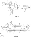
- Figure 1 is a schematic illustration of a system (which can be applied generically to a projector or to a 3D-detection system) in which a light source 1, typically a LASER source, generates a light beam 2 which, through an optics 3, is deflected by a pair of micromirrors 5, 6.
- the first micromirror 5 may, for example, be a horizontal micromirror, which rotates about a first axis A and generates a horizontal scan
- the second micromirror 6 may, for example, be a vertical micromirror, which rotates about a second transverse axis B, in particular perpendicular to the first axis A and generates a vertical scan.
- the combination of the movements of the two micromirrors 5, 6 causes the light beam 2 to perform a movement of complete two-dimensional scanning movement and, once projected onto a projection screen 7, to generate a two-dimensional image thereon.
- a system is described, for example, in WO 2010/067354 .
- Embodiments of a known type envisage that the micromirrors 5, 6 are mounted manually in an electronic apparatus for which they are designed, each being already fixed to a respective support, to form two respective mirror assemblies.
- an operator picks up two mirror assemblies, one for a horizontal micromirror and the other for a vertical micromirror, and positions the two assemblies into the desired condition of alignment (for example, a collimated light beam can be used to obtain the desired alignment).
- the operator applies a glue that can be polymerised via ultraviolet light, and the two mirror assemblies are fixed in the operating position.
- the two micromirrors horizontal and vertical, are assembled on a same metal frame and electrically wire-bonded to a respective electrical-connection element (flexible printed circuit) already fixed to the frame. Then the frame is bent so as to arrange the two micromirrors in the desired mutual angular arrangement.
- the bending step can be carried out automatically, without human intervention, using a forming press similar to the ones used in the semiconductor industry for shaping connection conductors in the packages of standard integrated circuits.
- the frame can be carried by a conveyor belt, together with a plurality of similar frames, and the individual frames can be separated after a single bending step.
- Patent document US 2017/052364 relates to an assembly body for micromirror chips, in particular to a mirror device.
- Patent document KR 2015/0042958 relates to an optical scanner using a mirror formed of a MEMS structure and a manufacturing method thereof.
- Patent document DE102014207899 relates to a module for a 3-D laser scanner, a 3-D laser scanner and a method for operating a module.
- the aim of the present invention is to provide an electronic module including two reflectors, in particular MEMS micromirrors, and a system including the electronic module, that will overcome the drawbacks of the prior art.
- an electronic module and a system including the electronic module are provided, as defined in the annexed claims.
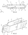
- Figure 2A shows, in cross-sectional view in a triaxial reference system of mutual orthogonal axes X, Y, Z, a module 30 that is to be mounted in an electronic apparatus (not illustrated).
- Figure 2B shows, in the same cross-sectional view and the same reference system as those of Figure 2A , a frame 31 of the module 30.
- Figure 2C is a perspective view, in the same reference system as that of Figures 2A and 2B , rigid-flexible electronic boards (with ends "broken", for greater clarity of representation) adapted to be coupled to the frame 31 to produce the module 30.
- the frame 31 is of a monolithic type and includes a first supporting portion 32 adapted to house a first die 35, and a second supporting portion 33 adapted to house a second die 36.
- the first supporting portion 32 is parallel to, and extends at a distance d G from, the second supporting portion 33.
- the frame 31 may be a single piece or may be made up of different elements joined (for example, soldered) together.
- the first supporting portion 32 is joined to the second supporting portion 33 at two connection regions 39', 39" provided with respective curved or bent portions, which join the first and second supporting portions 32, 33 together.
- a gap 31a is present that may be empty (i.e., air or some other gas is present) or filled with appropriate material (such as a liquid, or a gel, or the like), according to the specific application for which the module 30 is designed.
- the support portions 32, 33 and the connecting regions 39', 39" form a fluid-tight structure, i.e. the space 31a internally defined by them is fluidically isolated from the external environment.
- connection region 39" may likewise be omitted (i.e., it is not present), with the first and second support portions 32, 33 being connected to each other only at the connection region 39'.
- connection region 39" is releasably coupled to the first and second support portions 32, 33, for example by means of a suitable coupling-uncoupling system (e.g. of a plug-and-socket type), so that the connection region 39" can be removed if necessary and reinserted later.
- a suitable coupling-uncoupling system e.g. of a plug-and-socket type
- connection region 39" is a single piece with the first and second support portions 32, 33 (i.e., they form a monolithic block).
- connection region 39" is welded, or secured by glue or other adhesive, to the first and second support portions 32, 33, in a non-releasable manner.
- the frame 31 may be of metal material, e.g., anodized aluminium, or plastic material or some other material still, such as ceramic material or glass, or yet other materials chosen according to the need.
- the first die 35 manufactured, for example, using semiconductor micromachining techniques, integrates a first reflector 10, in particular a reflector produced using MEMS technology (also known as micromirror).
- the second die 36 in particular manufactured using semiconductor micromachining techniques, integrates a second reflector 20, in particular a reflector produced using MEMS technology (micromirror).
- the first and second reflectors 10, 20 are configured to be coupled to an activation or control system (common to both reflectors or dedicated to each reflector), which, when operated, causes the respective MEMS reflector to oscillate about a resting position.
- Micromirrors of this type are, for example, described in the U.S. patent No. 9,843,779 and in the U.S. patent application No. 2018/0180873 .
- the present invention is not limited to a specific technology of actuation of the reflector (piezoelectric, electrostatic, etc.).
- the first reflector 10 is configured to oscillate about a first oscillation axis
- the second reflector 20 is configured to oscillate about a respective second oscillation axis transverse (in particular, orthogonal) to the first oscillation axis.
- one or both of the first and second reflectors 10, 20 may be designed and configured to oscillate along both of the oscillation axes.
- one between the first and second reflectors 10, 20 may be of a fixed type (i.e., it does not oscillate).
- the frame 31 carries two electrical-connection structures 37, 38, one for each die 35, 36, obtained, for example, as flexible printed circuits and, more in particular, as rigid-flexible printed circuits of a known type, formed (in particular, embedded) in which are electrical-connection lines (not represented in detail).
- the electrical-connection structures 37, 38, and in particular the electrical-connection lines of each of them, are electrically connected to the dies 35, 36, e.g., via wire bonding.
- the electrical-connection structure 37 is coupled (e.g., glued) to a surface 32a of the first supporting portion 32; the electrical-connection structure 38 is coupled (e.g., glued) to a surface 33a of the second supporting portion 33.
- the first supporting portion 32 includes a housing 50, configured to house the first die 35
- the second supporting portion 33 includes a housing 52, configured to house the second die 36.
- the housing 50 and the housing 52 are through openings in the respective supporting portion 32, 33, and have a shape and dimensions such that the respective first and second dies 35, 36 insert into the respective housing 50, 51 in a stable manner, and the respective reflectors 10, 20 face the gap 31a and, consequently, the opposite supporting portion 32, 33.
- the first reflector 10, carried by the die 35 inserted in the housing 50 made in the first supporting portion 32 faces the second supporting portion 33.
- the second reflector 20, carried by the die 36 inserted in the housing 51 made in the second supporting portion 33 faces the first supporting portion 32.
- the second supporting portion 33 moreover has a through hole 54, configured to enable passage of an incoming light radiation, or beam, for example generated by a source of the type illustrated in Figure 1 and designated by the reference number 1 (e.g., a laser source).
- the light source is adapted to generate a beam that is to be deflected, in use, by the reflectors 10, 20, to be emitted at output from the module 30.
- the first supporting portion 32 moreover has a through hole 56, configured to enable passage of an outgoing beam, i.e., the beam reflected by the second reflector 20.
- the through hole 56 may be replaced by a generic opening in a different portion of the module 30 (for example, by eliminating the connection region 39" and leaving the module 30 open at the region 39" represented in the figures) .
- the through hole 54 has, in this embodiment, a substantially cylindrical shape with an axis 54a that forms an angle ⁇ of approximately 45° with the plane defined by the second portion 33 (in particular with the surface 33a of the second portion 33).
- angle ⁇ with respect to the values mentioned above, for example, reaching the value of 90° provided that the incoming beam can hit the first reflector 10 without being deflected by, or without interfering significantly with, the inner walls of the hole 54.
- the through hole 54 may have, as an alternative to the cylindrical shape, a conical shape or some other shape still chosen according to the need, in particular for limiting multiple reflections inside it.
- the hole 54 and the hole 56 may be internally coated with a non-reflective material, of a per se known type (e.g., belonging to the category of ARCs - Anti-Reflective Coatings).
- housings 50, 51 and, consequently, the reflectors 10, 20 are vertically staggered with respect to one another, i.e., staggered with respect to the axis Z orthogonal to the surfaces 32a and 33a.
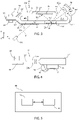
- reflecting surfaces of the reflectors 10, 20 do not directly face one another (i.e., they are not aligned along a same axis parallel to the axis Z), but are arranged in a position such that the first reflector 10 can receive an incoming beam B1 through the hole 54 (with a certain angle of reception, for example, 45°) and can deflect the beam B1 towards the second reflector 20 (reflected beam B2); in turn, the second reflector 20 can deflect the beam B2 received towards the output hole 56 of the module 30, to generate the beam B3a or B3b.
- the second reflector 20 is in this case of an oscillating type, and, by oscillating, can vary the angle at which the beam is directed towards the output hole 56, thus generating beams B3a, B3b having a desired angle or direction.
- Figure 3 moreover shows a generator 91 of the beam B1 (e.g., a laser or some other optical source of radiation or light beam), and a detector 94 of the emitted radiation or beam B3a-B3b.
- the type of the detector 94 varies according to the specific application and may not be present in the case of 3D detection of objects.
- a gap 31a is present between the supporting portions 32, 33.
- the supporting portions 32, 33 can be coupled together so that the gap 31a will be closed with respect to the external environment (so that the gap 31a can be filled by means of a liquid or gaseous fluid or be set in vacuum conditions in order to improve the dynamic control of the two mirrors and increase the reliability of the system during its service life, thanks to elimination of the air in contact with the mirrors).
- the supporting portions 32, 33 can be coupled together so that the gap 31a will be in fluid connection with the outside so as to be able to receive a (liquid or gaseous) fluid present in the external environment, for example, for carrying out an analysis of said fluid by analysing the interaction thereof with the beam reflected by the reflectors 10, 20.
- the gap 31a can be filled with a solid material, transparent for the beam received at input to, and transmitted at output from, the module 30, such as plastic resins or gels.
- the supporting portions 32, 33 of the frame 31 have a generically polygonal shape (in top view in the plane XY); in the examples illustrated in the figures, the supporting portions 32, 33 have a rectangular shape.
- connection region 39' comprises two connection arms or elements 60', 61' having a respective first end connected, respectively, to the first and second supporting portions 32, 33, and respective second ends connected together and to a portion 64.
- each connection arm 60', 61' forms a bending area that joins the first and second supporting portions 32, 33 to the portion 64.
- connection region 39" comprises two connection arms or elements 60", 61" having a respective first end connected (in a releasable or not releasable way, as said before) to the first supporting portion and to the second supporting portion 32, 33, respectively (on sides thereof opposite to the connection arms 60', 61'), and respective second ends connected together.
- each connection arm 60", 61" forms a further bending area that joins together the first and second supporting portions 32, 33.
- the electrical-connection structures 37, 38 extend, on opposite faces of the module 30, on the supporting portions 32, 33, along the connection arms 60', 61', and on the portion 64.
- the portion 64 is adapted to house connectors 68, 69, which are adapted to form an interface of connection between the module 30 and a system in which the module 30 is to be inserted or with which the module 30 is to be used.
- Each connector 68, 69 is electrically connected to the respective reflector 10, 20 by means of the respective electrical-connection lines integrated or present in the electrical-connection structures 37, 38, in particular for controlling the respective reflector 10, 20 in oscillation during use.
- the type, shape, and technical characteristics of these connectors 68, 69 do not form the subject of the present invention, and consequently are not described any further.
- production of the frame 31, which includes the first and second supporting portions 32, 33, the connection arms 60, 61, and the portion 64, can be carried out according to any available technology.
- the frame 31 can be obtained by soldering or gluing or fixing together in some other manner the first and second supporting portions 32, 33, the connection arms 60, 61, and the portion 64 (each of these elements being obtained according to any available technology, e.g., 3D printing, moulding, die-casting, etc.).
- the frame 31 may be obtained by making the first and second supporting portions 32, 33, the connection arms 60, 61, and the portion 64 of a single piece, for example, using processes of die-casting of metal material.
- the frame 31 may be obtained via known machining processes, starting from a solid piece of material and appropriately modelling it by means of progressive removal of material, until the desired final shape is obtained.
- the frame 31 may be obtained by making the first and second supporting portions 32, 33, the connection arms 60, 61, and the portion 64 in a single piece, for example, using processes of moulding of plastic or polymeric material.
- the frame 31 may be obtained by making the first and second supporting portions 32, 33, the connection arms 60, 61, and the portion 64, in a single piece using 3D printing. It may be noted that 3D-printing technologies currently available enable manufacturing of both the frame 31 and the electrical connections adapted to connect the reflectors 10, 20 to the connectors 68, 69, by printing respective materials. Consequently, in this case, it is not necessary to use a flexible or rigid-flexible printed circuit that presents electrical connections or wires adapted to connect the dies 35, 36 to the connectors 68, 69.
- alignment elements 70 are optionally present, here illustrated in the form of small pillars or pins that protrude from the frame 31, along one or more of the first and second supporting portions 32, 33, the connection arms 60, 61, and the portion 64; each electrical-connection structure 37, 38 has alignment holes (not illustrated), configured to couple to respective alignment elements 70. This facilitates the steps of coupling between the electrical-connection structures 37, 38 and the frame 31, in particular alignment between the dies 35, 36 and the housings 50, 51.
- FIG 4 is a schematic illustration of the electrical-connection structure 37, which carries the first die 35.
- the electrical-connection structure 37 has a first face 37a and a second face 37b opposite to one another.
- the electrical-connection structure 37 is, for example, a rigid-flexible board of an FCCL (Flex Copper Clad Laminate) type, with four layers (also known as 4L), i.e., having four metal layers that can be used for the electrical connections discussed previously.
- FCCL Flexible Copper Clad Laminate
- 4L four layers
- the electrical-connection structure 37 represented is of a rigid-flexible type; i.e., it comprises a rigid portion 37' having a stiffness greater than that of a flexible portion 37" that is contiguous to, and extends as a prolongation of, the rigid region 37'.
- the next step is formation (e.g., via gluing) of an element 80 at an end portion of the flexible portion 37", on the face 37b.
- the element 80 is, for example, made of metal, for instance, copper or aluminium, or other materials such as BT/FR4 or plastic materials, with a thickness of between 200 and 300 ⁇ m, and has the function of increasing locally the stiffness of the flexible portion 37" to favour handling thereof. This step can be omitted in the case where no difficulties of handling are encountered.
- the connector 68 is coupled (e.g., soldered, glued, or fixed in some other manner) to the face 37a of the electrical-connection structure 37, at the flexible portion 37" and in particular at the element 80 (as has been said, on the face 37a opposite to the face 37b that houses the element 80).
- the die 35 is coupled (e.g., glued or fixed in some other manner) to the rigid portion 37', on the face 37b.
- Electrical-connection wires 82 are formed for connecting pads for control of the die 35 to the electrical connections present on the electrical-connection structure 37 so as to provide the electrical connection necessary for controlling the reflector 10.
- the electrical-connection wires 82 are coated with a protective material 84, for example, epoxy-based or silicone-based resins.
- the face 37b of the electrical-connection structure 37 is the one that is arranged directly facing the first supporting portion 32.
- the input hole 54 and/or the output hole 56 may optionally include a respective lens, through which the beam entering or leaving, respectively, the module 30 passes.
- This lens for example, has the function of collimating the incoming beam in the case of the hole 54; and of correcting the divergence, either leading to collimation or increasing the divergence of the outgoing beam according to the different applications, in the case of the output hole 56.
- the module 30 described according to the present invention can be used in a time-of-flight device/photographic camera for carrying out 3D detection, for example, for applications on smartphones, such as facial recognition.
- direct or sinusoidal short light flashes are generated by an emitter towards the input hole 54; the beam entering the module 30 is appropriately reflected by the reflectors 10, 20 and is emitted at output through the hole 56; said emitted beam strikes an object and is reflected back, once again entering the module 30 through the hole 56 and, following the reverse reflection path, is made to exit through the hole 54 (received beam).
- This example does not find application where the receiver is separate from the transmitter.
- the received beam is then captured by a detector to be analysed.
- the travel time of the beam from the emitter to the object and back to the detector is calculated by processing means (for example, a processor, or a processing unit).
- processing means for example, a processor, or a processing unit.
- the co-ordinates measured are then used for generating a 3D image of the object, in a manner that is known and does not form part of the present invention.
- the module 30 can also be used in the context of structured-light applications for 3D detection.
- the detector is preferably a CMOS sensor formed by an array of pixels, adapted to detect an image from the incoming beam.
- Processing algorithms known in the prior art can be used for acquiring information from the image detected for carrying out 3D detection, such as facial recognition.
- modules 30 include the use of the module 30 in LIDAR systems or devices that can be used, for example, in applications for autonomous driving of vehicles.
- modules 30 include the use of the module 30 in systems or applications for the projection of images (e.g., picoprojectors).
- FIG. 5 is a schematic illustration of a system 90, in particular a 3D scanning device or 3D scanner, which includes at least one module 30, operatively coupled to a processing unit 92 that is configured for carrying out 3D detection based on a structured-light approach, a time-of-flight approach, or the like.
- the processing unit 92 is configured to calculate a travel time between a first instant, corresponding to generation of a first radiation by the emitter, and a second instant, corresponding to the detection of a second radiation received by the detector (i.e., the travel time of the beam from the emitter to the object and back to the detector). Irrespective of the approach used, a 3D image of the object can be reconstructed by the processing unit 92, in a per se known manner.
- the module 30 can be provided, to be mounted in electronic apparatuses or systems, already complete with the two micromirrors arranged in the desired mutual angular and spatial position. In this manner, mounting can be carried out automatically by pick-and-place machines, so reducing the costs of assembly and the risks of erroneous positioning, and thus increasing yield.
Landscapes
- Physics & Mathematics (AREA)
- General Physics & Mathematics (AREA)
- Optics & Photonics (AREA)
- Micromachines (AREA)
- Led Device Packages (AREA)
- Gyroscopes (AREA)
- Mechanical Light Control Or Optical Switches (AREA)
Abstract
Description
- The present invention relates to an electronic module including reflectors, in particular MEMS micromirrors, and a system including, or integrating, the electronic module.
- Micromechanical mirror structures are known, made, at least in part, of semiconductor materials and obtained using MEMS (MicroElectroMechanical Systems) technology. Such micromechanical structures are typically integrated in portable apparatuses, such as, for example, portable computers, laptops, notebooks (including ultra-thin notebooks), PDAs, tablets, and smartphones, for optical applications, in particular for directing with desired modalities beams of light radiation generated by a light source.
- Thanks to the small dimensions, such structures make it possible to meet stringent requisites as regards occupation of space, in terms of area and thickness.
- For instance, micromechanical mirror structures (or micromirrors, typically obtained with MEMS technology) are used in miniaturized projector modules (the so-called picoprojectors), which are able to project images at a distance or generate desired patterns of light.
- In combination with an image-capturing module, a projector module of this kind makes it possible, for example, to obtain a three-dimensional (3D) photographic or video camera for the formation of three-dimensional images.
- The aforesaid micromechanical mirror structures generally include a mirror element, obtained starting from a body of semiconductor material so as to be mobile, for example, with movement of tilting or rotation, to direct the incident light beam in a desired manner; and a supporting element, which is also obtained starting from a body of semiconductor material, coupled to the mirror element having supporting and handling functions. A cavity is made in the supporting element, set underneath and in a position corresponding to the mirror element, so as to enable freedom of movement thereof for inclination or rotation thereof.
- Picoprojectors of a known type use micromirrors capable of rotating about two axes in order to carry out a movement of scanning of a two-dimensional area. In particular, in some solutions, micromirror systems comprise a pair of micromirrors governed so as to rotate about two mutually perpendicular rotation axes.
- Moreover, with the introduction of the technology of in-depth detection, 3D detection is now widely used on smartphones and portable devices in general. In particular, the technology is expected to innovate safety methods through facial recognition.
- One of the known methods for implementing 3D detection is based on a time-of-flight (ToF) approach. A typical ToF architecture includes an infrared (IR) source configured to generate an IR pulse towards an object (emitted beam). In some applications, a beam reflected by the object is received by micromirrors which direct the reflected beam towards a detector. In other applications, the micromirrors are arranged at the level of the transmitter so as to generate an array of dots that strikes the target, and the receiver receives the response pulses. The depth is calculated by measuring the time (direct ToF) or the phase offset (indirect ToF) between the emitted beam and the reflected beam. Another known method for implementing 3D detection is based on structured light. In this case, a known pattern is projected onto an object; the pattern thus projected is distorted by the object and an analysis of the distortion of the pattern of light can be used for calculating a value of depth and achieving a geometrical reconstruction of the shape of the object.
- For instance,
Figure 1 is a schematic illustration of a system (which can be applied generically to a projector or to a 3D-detection system) in which alight source 1, typically a LASER source, generates alight beam 2 which, through anoptics 3, is deflected by a pair ofmicromirrors 5, 6. The first micromirror 5 may, for example, be a horizontal micromirror, which rotates about a first axis A and generates a horizontal scan, and thesecond micromirror 6 may, for example, be a vertical micromirror, which rotates about a second transverse axis B, in particular perpendicular to the first axis A and generates a vertical scan. The combination of the movements of the twomicromirrors 5, 6 causes thelight beam 2 to perform a movement of complete two-dimensional scanning movement and, once projected onto aprojection screen 7, to generate a two-dimensional image thereon. Such a system is described, for example, inWO 2010/067354 . - Embodiments of a known type envisage that the
micromirrors 5, 6 are mounted manually in an electronic apparatus for which they are designed, each being already fixed to a respective support, to form two respective mirror assemblies. - During mounting, an operator picks up two mirror assemblies, one for a horizontal micromirror and the other for a vertical micromirror, and positions the two assemblies into the desired condition of alignment (for example, a collimated light beam can be used to obtain the desired alignment). Next, the operator applies a glue that can be polymerised via ultraviolet light, and the two mirror assemblies are fixed in the operating position.
- The above type of assembly is slow, difficult, and considerably subject to errors. It follows that, with this method, the productivity and yield in terms of a pieces properly mounted is not optimal.
- Other embodiments, for example, the one described in
EP3206071 , envisage that the two micromirrors, horizontal and vertical, are assembled on a same metal frame and electrically wire-bonded to a respective electrical-connection element (flexible printed circuit) already fixed to the frame. Then the frame is bent so as to arrange the two micromirrors in the desired mutual angular arrangement. The bending step can be carried out automatically, without human intervention, using a forming press similar to the ones used in the semiconductor industry for shaping connection conductors in the packages of standard integrated circuits. The frame can be carried by a conveyor belt, together with a plurality of similar frames, and the individual frames can be separated after a single bending step. - Patent document
US 2017/052364 relates to an assembly body for micromirror chips, in particular to a mirror device. - Patent document
KR 2015/0042958 - Patent document
DE102014207899 relates to a module for a 3-D laser scanner, a 3-D laser scanner and a method for operating a module. - However, the above-mentioned issues are not solved.
- The need is consequently felt in the art for a technical solution that will overcome the problems referred to above without having an impact on performance.
- The aim of the present invention is to provide an electronic module including two reflectors, in particular MEMS micromirrors, and a system including the electronic module, that will overcome the drawbacks of the prior art.
- According to the present invention an electronic module and a system including the electronic module are provided, as defined in the annexed claims.
- For a better understanding of the present invention, preferred embodiments thereof are now described purely by way of non-limiting example and with reference to the attached drawings, wherein:
-
Figure 1 is a schematic perspective view of an electronic system that can be used as picoprojector or for 3D-sensing applications, according to an embodiment of a known type; -
Figure 2A illustrates, in cross-sectional view, a module including a supporting element that carries two electronic boards of a rigid-flexible type, mounted on which are respective reflectors, in particular micromirrors, and corresponding electrical connectors, according to an aspect of the present invention; -
Figure 2B illustrates, in cross-sectional view, the supporting element ofFigure 2A ; -
Figure 2C illustrates, in perspective view, the two electronic boards, mounted on which are respective reflectors, of the module ofFigure 2A ; -
Figure 3 illustrates, in schematic cross-sectional view, the module ofFigure 2A in a condition of use; -
Figure 4 illustrates, schematically and in cross-sectional view, a board of a rigid-flexible type adapted to be used for mounting a reflector, in particular a micromirror, and a corresponding connector, according to an aspect of the present invention; and -
Figure 5 is a schematic representation, by means of functional blocks, of a system that integrates or uses the module ofFigure 2A . -
Figure 2A shows, in cross-sectional view in a triaxial reference system of mutual orthogonal axes X, Y, Z, amodule 30 that is to be mounted in an electronic apparatus (not illustrated). -
Figure 2B shows, in the same cross-sectional view and the same reference system as those ofFigure 2A , aframe 31 of themodule 30. -
Figure 2C is a perspective view, in the same reference system as that ofFigures 2A and2B , rigid-flexible electronic boards (with ends "broken", for greater clarity of representation) adapted to be coupled to theframe 31 to produce themodule 30. - With joint reference to
Figures 2A-2C , theframe 31 is of a monolithic type and includes a first supportingportion 32 adapted to house afirst die 35, and a second supportingportion 33 adapted to house asecond die 36. The first supportingportion 32 is parallel to, and extends at a distance dG from, the second supportingportion 33. - It is evident that, in respective embodiments, the
frame 31 may be a single piece or may be made up of different elements joined (for example, soldered) together. - The first supporting
portion 32 is joined to the second supportingportion 33 at twoconnection regions 39', 39" provided with respective curved or bent portions, which join the first and second supportingportions portions gap 31a is present that may be empty (i.e., air or some other gas is present) or filled with appropriate material (such as a liquid, or a gel, or the like), according to the specific application for which themodule 30 is designed. - In an embodiment, the
support portions connecting regions 39', 39" form a fluid-tight structure, i.e. thespace 31a internally defined by them is fluidically isolated from the external environment. - In one embodiment, the
connection region 39" may likewise be omitted (i.e., it is not present), with the first andsecond support portions - In a further embodiment, the
connection region 39" is releasably coupled to the first andsecond support portions connection region 39" can be removed if necessary and reinserted later. - In a further embodiment, the
connection region 39" is a single piece with the first andsecond support portions 32, 33 (i.e., they form a monolithic block). - In a further embodiment, the
connection region 39" is welded, or secured by glue or other adhesive, to the first andsecond support portions - The
frame 31 may be of metal material, e.g., anodized aluminium, or plastic material or some other material still, such as ceramic material or glass, or yet other materials chosen according to the need. - The
first die 35, manufactured, for example, using semiconductor micromachining techniques, integrates afirst reflector 10, in particular a reflector produced using MEMS technology (also known as micromirror). The second die 36, in particular manufactured using semiconductor micromachining techniques, integrates asecond reflector 20, in particular a reflector produced using MEMS technology (micromirror). The first andsecond reflectors U.S. patent No. 9,843,779 U.S. patent application No. 2018/0180873 . It is in any case possible to use other types of reflectors or micromirrors, as will be evident to the person skilled in the art. In particular, the present invention is not limited to a specific technology of actuation of the reflector (piezoelectric, electrostatic, etc.). - The
first reflector 10 is configured to oscillate about a first oscillation axis, whereas thesecond reflector 20 is configured to oscillate about a respective second oscillation axis transverse (in particular, orthogonal) to the first oscillation axis. - Alternatively, in a further embodiment, one or both of the first and
second reflectors - Alternatively, in a further embodiment, one between the first and
second reflectors - The
frame 31 carries two electrical-connection structures connection structures connection structure 37 is coupled (e.g., glued) to asurface 32a of the first supportingportion 32; the electrical-connection structure 38 is coupled (e.g., glued) to asurface 33a of the second supportingportion 33. - It is evident that, if one between the first and
second reflectors connection structure - The first supporting
portion 32 includes ahousing 50, configured to house thefirst die 35, and the second supportingportion 33 includes ahousing 52, configured to house thesecond die 36. Thehousing 50 and thehousing 52 are through openings in the respective supportingportion respective housing 50, 51 in a stable manner, and therespective reflectors gap 31a and, consequently, the opposite supportingportion first reflector 10, carried by the die 35 inserted in thehousing 50 made in the first supportingportion 32, faces the second supportingportion 33. Likewise, thesecond reflector 20, carried by the die 36 inserted in the housing 51 made in the second supportingportion 33, faces the first supportingportion 32. - The second supporting
portion 33 moreover has a throughhole 54, configured to enable passage of an incoming light radiation, or beam, for example generated by a source of the type illustrated inFigure 1 and designated by the reference number 1 (e.g., a laser source). The light source is adapted to generate a beam that is to be deflected, in use, by thereflectors module 30. For this purpose, the first supportingportion 32 moreover has a throughhole 56, configured to enable passage of an outgoing beam, i.e., the beam reflected by thesecond reflector 20. The throughhole 56 may be replaced by a generic opening in a different portion of the module 30 (for example, by eliminating theconnection region 39" and leaving themodule 30 open at theregion 39" represented in the figures) . - The through
hole 54 has, in this embodiment, a substantially cylindrical shape with anaxis 54a that forms an angle β of approximately 45° with the plane defined by the second portion 33 (in particular with thesurface 33a of the second portion 33). The value of the angle β may in any case vary and be chosen in the range between 25° and 65° (where β=0° means that theaxis 54a of thehole 54 is parallel to thesurface 33a of the second supportingportion 33, and β=90° means that theaxis 54a of thehole 54 is orthogonal to thesurface 33a of the second supporting portion 33). However, it is possible to vary the angle β with respect to the values mentioned above, for example, reaching the value of 90° provided that the incoming beam can hit thefirst reflector 10 without being deflected by, or without interfering significantly with, the inner walls of thehole 54. - The through
hole 54 may have, as an alternative to the cylindrical shape, a conical shape or some other shape still chosen according to the need, in particular for limiting multiple reflections inside it. - The
hole 54 and thehole 56 may be internally coated with a non-reflective material, of a per se known type (e.g., belonging to the category of ARCs - Anti-Reflective Coatings). - Furthermore, it may be noted that the
housings 50, 51 and, consequently, thereflectors surfaces Figure 3 , reflecting surfaces of thereflectors first reflector 10 can receive an incoming beam B1 through the hole 54 (with a certain angle of reception, for example, 45°) and can deflect the beam B1 towards the second reflector 20 (reflected beam B2); in turn, thesecond reflector 20 can deflect the beam B2 received towards theoutput hole 56 of themodule 30, to generate the beam B3a or B3b. As illustrated inFigure 3 , thesecond reflector 20 is in this case of an oscillating type, and, by oscillating, can vary the angle at which the beam is directed towards theoutput hole 56, thus generating beams B3a, B3b having a desired angle or direction. -
Figure 3 moreover shows agenerator 91 of the beam B1 (e.g., a laser or some other optical source of radiation or light beam), and adetector 94 of the emitted radiation or beam B3a-B3b. The type of thedetector 94 varies according to the specific application and may not be present in the case of 3D detection of objects. - As has been anticipated, a
gap 31a is present between the supportingportions portions gap 31a will be closed with respect to the external environment (so that thegap 31a can be filled by means of a liquid or gaseous fluid or be set in vacuum conditions in order to improve the dynamic control of the two mirrors and increase the reliability of the system during its service life, thanks to elimination of the air in contact with the mirrors). Alternatively, the supportingportions gap 31a will be in fluid connection with the outside so as to be able to receive a (liquid or gaseous) fluid present in the external environment, for example, for carrying out an analysis of said fluid by analysing the interaction thereof with the beam reflected by thereflectors - Alternatively, the
gap 31a can be filled with a solid material, transparent for the beam received at input to, and transmitted at output from, themodule 30, such as plastic resins or gels. - The supporting
portions frame 31 have a generically polygonal shape (in top view in the plane XY); in the examples illustrated in the figures, the supportingportions - In the embodiment illustrated, the connection region 39' comprises two connection arms or elements 60', 61' having a respective first end connected, respectively, to the first and second supporting
portions portion 64. In this manner, each connection arm 60', 61' forms a bending area that joins the first and second supportingportions portion 64. - In addition, also the
connection region 39" comprises two connection arms orelements 60", 61" having a respective first end connected (in a releasable or not releasable way, as said before) to the first supporting portion and to the second supportingportion connection arm 60", 61" forms a further bending area that joins together the first and second supportingportions - As may be noted from
Figure 2A , the electrical-connection structures module 30, on the supportingportions portion 64. In particular, theportion 64 is adapted to houseconnectors module 30 and a system in which themodule 30 is to be inserted or with which themodule 30 is to be used. Eachconnector respective reflector connection structures respective reflector connectors - It may be noted that production of the
frame 31, which includes the first and second supportingportions connection arms portion 64, can be carried out according to any available technology. - For instance, the
frame 31 can be obtained by soldering or gluing or fixing together in some other manner the first and second supportingportions connection arms - Alternatively, the
frame 31 may be obtained by making the first and second supportingportions connection arms portion 64 of a single piece, for example, using processes of die-casting of metal material. - Alternatively, the
frame 31 may be obtained via known machining processes, starting from a solid piece of material and appropriately modelling it by means of progressive removal of material, until the desired final shape is obtained. - Alternatively, the
frame 31 may be obtained by making the first and second supportingportions connection arms portion 64 in a single piece, for example, using processes of moulding of plastic or polymeric material. - Alternatively, the
frame 31 may be obtained by making the first and second supportingportions connection arms portion 64, in a single piece using 3D printing. It may be noted that 3D-printing technologies currently available enable manufacturing of both theframe 31 and the electrical connections adapted to connect thereflectors connectors connectors - With reference to
Figure 2B ,alignment elements 70 are optionally present, here illustrated in the form of small pillars or pins that protrude from theframe 31, along one or more of the first and second supportingportions connection arms portion 64; each electrical-connection structure respective alignment elements 70. This facilitates the steps of coupling between the electrical-connection structures frame 31, in particular alignment between the dies 35, 36 and thehousings 50, 51. -
Figure 4 is a schematic illustration of the electrical-connection structure 37, which carries thefirst die 35. The electrical-connection structure 37 has afirst face 37a and asecond face 37b opposite to one another. The electrical-connection structure 37 is, for example, a rigid-flexible board of an FCCL (Flex Copper Clad Laminate) type, with four layers (also known as 4L), i.e., having four metal layers that can be used for the electrical connections discussed previously. Alternatively, it is also possible to use a rigid-flexible board of an FCCL type with double metal layer (2L), according to the need. It is evident that these are just two possible non-limiting examples, and other types of flexible or rigid-flexible boards or substrates can be used. - With reference to
Figure 4 , the electrical-connection structure 37 represented is of a rigid-flexible type; i.e., it comprises a rigid portion 37' having a stiffness greater than that of aflexible portion 37" that is contiguous to, and extends as a prolongation of, the rigid region 37'. After the electrical-connection structure 37 has been pre-arranged, the next step is formation (e.g., via gluing) of anelement 80 at an end portion of theflexible portion 37", on theface 37b. Theelement 80 is, for example, made of metal, for instance, copper or aluminium, or other materials such as BT/FR4 or plastic materials, with a thickness of between 200 and 300 µm, and has the function of increasing locally the stiffness of theflexible portion 37" to favour handling thereof. This step can be omitted in the case where no difficulties of handling are encountered. - Then, the
connector 68 is coupled (e.g., soldered, glued, or fixed in some other manner) to theface 37a of the electrical-connection structure 37, at theflexible portion 37" and in particular at the element 80 (as has been said, on theface 37a opposite to theface 37b that houses the element 80). - Then, the
die 35 is coupled (e.g., glued or fixed in some other manner) to the rigid portion 37', on theface 37b. Electrical-connection wires 82 are formed for connecting pads for control of the die 35 to the electrical connections present on the electrical-connection structure 37 so as to provide the electrical connection necessary for controlling thereflector 10. The electrical-connection wires 82 are coated with aprotective material 84, for example, epoxy-based or silicone-based resins. Theface 37b of the electrical-connection structure 37 is the one that is arranged directly facing the first supportingportion 32. - Similar operations, not described in detail in so far as they are in themselves evident, are carried out on the electrical-
connection structure 38, for coupling theconnector 69 and the die 36 of the electrical-connection structure 38. - According to one embodiment, the
input hole 54 and/or theoutput hole 56 may optionally include a respective lens, through which the beam entering or leaving, respectively, themodule 30 passes. This lens, for example, has the function of collimating the incoming beam in the case of thehole 54; and of correcting the divergence, either leading to collimation or increasing the divergence of the outgoing beam according to the different applications, in the case of theoutput hole 56. - The
module 30 described according to the present invention can be used in a time-of-flight device/photographic camera for carrying out 3D detection, for example, for applications on smartphones, such as facial recognition. In this context, direct or sinusoidal short light flashes are generated by an emitter towards theinput hole 54; the beam entering themodule 30 is appropriately reflected by thereflectors hole 56; said emitted beam strikes an object and is reflected back, once again entering themodule 30 through thehole 56 and, following the reverse reflection path, is made to exit through the hole 54 (received beam). This example does not find application where the receiver is separate from the transmitter. The received beam is then captured by a detector to be analysed. The travel time of the beam from the emitter to the object and back to the detector is calculated by processing means (for example, a processor, or a processing unit). The co-ordinates measured are then used for generating a 3D image of the object, in a manner that is known and does not form part of the present invention. - The
module 30 can also be used in the context of structured-light applications for 3D detection. In this case, the detector is preferably a CMOS sensor formed by an array of pixels, adapted to detect an image from the incoming beam. Processing algorithms known in the prior art can be used for acquiring information from the image detected for carrying out 3D detection, such as facial recognition. - Other possible applications include the use of the
module 30 in LIDAR systems or devices that can be used, for example, in applications for autonomous driving of vehicles. - Yet other applications include the use of the
module 30 in systems or applications for the projection of images (e.g., picoprojectors). -
Figure 5 is a schematic illustration of asystem 90, in particular a 3D scanning device or 3D scanner, which includes at least onemodule 30, operatively coupled to aprocessing unit 92 that is configured for carrying out 3D detection based on a structured-light approach, a time-of-flight approach, or the like. For instance, in the case of the time-of-flight approach, theprocessing unit 92 is configured to calculate a travel time between a first instant, corresponding to generation of a first radiation by the emitter, and a second instant, corresponding to the detection of a second radiation received by the detector (i.e., the travel time of the beam from the emitter to the object and back to the detector). Irrespective of the approach used, a 3D image of the object can be reconstructed by theprocessing unit 92, in a per se known manner. - From an examination of the characteristics of the invention provided according to the present description, the advantages deriving therefrom are evident.
- By integrating all the components in a module at the level of packaging structure, the volumes of the solution are reduced and optimized.
- In addition, the
module 30 can be provided, to be mounted in electronic apparatuses or systems, already complete with the two micromirrors arranged in the desired mutual angular and spatial position. In this manner, mounting can be carried out automatically by pick-and-place machines, so reducing the costs of assembly and the risks of erroneous positioning, and thus increasing yield. - Assembly of the mirror assemblies in electronic apparatuses using automatic machines, without human intervention, reduces costs and increases productivity.
- Finally, it is clear that modifications and variations may be made to what has been described and illustrated herein, without thereby departing from the scope of the present invention, as defined in the annexed claims.
Claims (23)
- An electronic module (30) comprising:a first die (35) of semiconductor material including a first reflector (10);a second die (36) of semiconductor material including a second reflector (20); anda frame (31) including a first supporting portion and a second supporting portion (32, 33) parallel to one another;wherein the first and second dies (35, 36) are carried, respectively, by the first and second supporting portions (32, 33) and are respectively arranged so that the first reflector (10) faces the second supporting portion and the second reflector (20) faces the first supporting portion (32) .
- The electronic module according to claim 1, wherein the first and second reflectors (10, 20) are staggered with respect to one another.
- The electronic module according to any one of the preceding claims, wherein the first and second supporting portions are arranged at a mutual distance (dG) apart so as to define a gap (31a) inside the frame (31).
- The electronic module according to claim 3, wherein the first supporting portion (32) comprises a first cavity (50) adapted to house at least in part the first die (35) so that the first reflector faces the gap (31a), and a first through opening (56) passing through the first supporting portion (32) laterally to the first cavity (50);
and wherein the second supporting portion (33) comprises a second cavity (51) adapted to house at least in part the second die (36) so that the second reflector faces the gap (31a), and a second through opening (54) passing through the second supporting portion (33) laterally to the second cavity. - The electronic module according to any one of the preceding claims, wherein the first supporting portion (32) further comprises a first through opening (56) arranged laterally to the first cavity (50);
and wherein the second supporting portion (33) further comprises a second through opening (54) arranged laterally to the second cavity. - The electronic module according to claim 5, wherein said first reflector (10), said second reflector (20), said first opening (56), and said second opening (54) are mutually arranged so that, in use, a radiation or beam follows the following path:i. it enters the gap (31a) through one between the first and second openings (56, 54),ii. it strikes the first reflector or the second reflector (10, 20), respectively,iii. it is deflected towards the other one between the first reflector and the second reflector (10, 20); andiv. it exits the gap (31a) through the other one between the first opening and the second opening (56, 54).
- The electronic module according to claim 5 or claim 6, wherein at least one between the first and second openings (56, 54) has inner walls coated with anti-reflective material and/or shaped so as to limit multiple reflections within it.
- The electronic module according to any one of the preceding claims, wherein the frame (31) is monolithic.
- The electronic module according to any one of the preceding claims, wherein the first and second supporting portions (32, 33) are joined together by a first connection portion (39') having a bending area (60', 61') that joins the first and second supporting portions (32, 33) to a common connection portion (64).
- The electronic module according to claim 9, wherein the first and second supporting portions (32, 33) are moreover coupled to a second connection portion (39") having a respective bending area (60", 61") that joins the first and second supporting portions (32, 33) together,
said second connection portion (39") being coupled to the first and second supporting portions (32, 33) in a releasable way or, alterbnatively, in a non-releasable way. - The electronic module according to claim 9 or claim 10, wherein the first and second supporting portions have a rectangular shape and the first and second connection portions (39', 39") extend at opposite sides of the first and second supporting portions.
- The electronic module according to anyone of claims 9-11, wherein the first and second connection portions (39', 39") are not coplanar with the first and second supporting portions (32, 33).
- The electronic module according to any one of the preceding claims, wherein the first and second supporting portions (32, 33) each carry a first electrical-connection element and a second electrical-connection element (37, 38), respectively, the first die being coupled to the first electrical-connection element and the second die being coupled to the second electrical-connection element.
- The electronic module according to claim 13, wherein the first electrical-connection element (37) is a board of a rigid-flexible type, the first die being coupled to the rigid portion of the first electrical-connection element (37); and wherein the second electrical-connection element (38) is a board of a rigid-flexible type, the second die being coupled to the rigid portion of the second electrical-connection element (38).
- The electronic module according to claim 13 or claim 14, wherein the first electrical-connection element (37) moreover carries a first electrical connector (68) on the flexible portion, and the second electrical-connection element (38) moreover carries a second electrical connector (69) on the flexible portion.
- The electronic module according to claims 9 and 15, wherein the flexible portion that carries the first connector (68) extends on a first side of the connection portion (64), and the flexible portion that carries the second connector (69) extends on a second side, opposite to the first side, of the connection portion (64).
- The electronic module according to claim 13, wherein the first electrical-connection element (37) includes a conductive track printed on the first supporting portion (32), and the second electrical-connection element (38) includes a conductive track printed on the second supporting portion (32).
- The electronic module according to claims 9 and 17, wherein the connection portion (64) carries a first electrical connector and a second electrical connector (68, 69), said conductive track on the first supporting portion being electrically connected to the first electrical connector and said conductive track on the second supporting portion being electrically connected to the second connector (69).
- The electronic module according to any one of the preceding claims, wherein the first and second reflectors (10, 20) are micromirror reflectors, and at least one between the first and second reflectors (10, 20) is configured to oscillate about a resting position.
- The electronic module according to claim 3, or according to any one of claims 4-18 when depending upon claim 3, wherein the first and second supporting portions are hermetically coupled together so that said gap (31a) is fluidically isolated with respect to an environment external to the electronic module, and wherein the gap (31a) is filled by a liquid or gaseous fluid.
- A system (90) including:- an electronic module (2; 40; 50; 60) according to any one of the claims 1 to 20;- a generator of a first light radiation or beam (B1), arranged and configured to supply said first light radiation or beam (B1) towards the first reflector (10);- a detector configured to receive a second light radiation or reflected beam from the second reflector (20) and generate a transduced signal; and- a processing unit (92), operatively coupled to the detector, configured to carry out processing of the transduced signal.
- The system according to claim 21, wherein said system is one of the following: a picoprojector, a 3D-detection system, a LIDAR system.
- The system according to claim 22, wherein when the system is a 3D-detection system, said processing comprises carrying out a 3D detection of an object or a subject through a structured-light approach and/or a time-of-flight approach.
Applications Claiming Priority (1)
| Application Number | Priority Date | Filing Date | Title |
|---|---|---|---|
| IT102020000022715A IT202000022715A1 (en) | 2020-09-25 | 2020-09-25 | INTEGRATED ELECTRONIC MODULE INCLUDING TWO MICROMIRRORS, AND SYSTEM THAT INCLUDE THE ELECTRONIC MODULE |
Publications (2)
| Publication Number | Publication Date |
|---|---|
| EP3974889A1 true EP3974889A1 (en) | 2022-03-30 |
| EP3974889B1 EP3974889B1 (en) | 2024-08-28 |
Family
ID=73643286
Family Applications (1)
| Application Number | Title | Priority Date | Filing Date |
|---|---|---|---|
| EP21198930.6A Active EP3974889B1 (en) | 2020-09-25 | 2021-09-24 | Integrated electronic module including two micromirrors, and system including the electronic module |
Country Status (3)
| Country | Link |
|---|---|
| US (1) | US12204092B2 (en) |
| EP (1) | EP3974889B1 (en) |
| IT (1) | IT202000022715A1 (en) |
Citations (8)
| Publication number | Priority date | Publication date | Assignee | Title |
|---|---|---|---|---|
| WO2010067354A1 (en) | 2008-12-14 | 2010-06-17 | Btendo Ltd. | Device and method for scanning images by laser projector |
| KR20150042958A (en) | 2013-10-14 | 2015-04-22 | 광주과학기술원 | The optical scanner and manufacturing method thereof |
| DE102014207899A1 (en) | 2014-04-28 | 2015-10-29 | Robert Bosch Gmbh | 3D fine laser scanner |
| US20170052364A1 (en) | 2014-05-07 | 2017-02-23 | Robert Bosch Gmbh | Assembly body for micromirror chips, mirror device and production method for a mirror device |
| EP3206071A1 (en) | 2016-02-12 | 2017-08-16 | STMicroelectronics Srl | Mirror group, in particular for a picoprojector, comprising micromirrors made using the mems technology |
| US9843779B2 (en) | 2015-11-30 | 2017-12-12 | Stmicroelectronics S.R.L. | Resonant biaxial MEMS reflector with piezoelectric actuators, and projective MEMS system including the same |
| US20180180873A1 (en) | 2016-12-28 | 2018-06-28 | Stmicroelectronics S.R.L. | Mems device with piezoelectric actuation, a projective mems system including the mems device and related control method |
| EP3712660A1 (en) * | 2019-03-22 | 2020-09-23 | STMicroelectronics S.r.l. | Integrated electronic module for 3d sensing applications, and 3d scanning device including the integrated electronic module |
Family Cites Families (2)
| Publication number | Priority date | Publication date | Assignee | Title |
|---|---|---|---|---|
| CN112004000A (en) * | 2019-05-27 | 2020-11-27 | 三赢科技(深圳)有限公司 | Light-emitting device and image acquisition device using same |
| CN114252989A (en) | 2020-09-25 | 2022-03-29 | 意法半导体股份有限公司 | Integrated electronic module comprising two micromirrors and system comprising an electronic module |
-
2020
- 2020-09-25 IT IT102020000022715A patent/IT202000022715A1/en unknown
-
2021
- 2021-09-21 US US17/480,634 patent/US12204092B2/en active Active
- 2021-09-24 EP EP21198930.6A patent/EP3974889B1/en active Active
Patent Citations (8)
| Publication number | Priority date | Publication date | Assignee | Title |
|---|---|---|---|---|
| WO2010067354A1 (en) | 2008-12-14 | 2010-06-17 | Btendo Ltd. | Device and method for scanning images by laser projector |
| KR20150042958A (en) | 2013-10-14 | 2015-04-22 | 광주과학기술원 | The optical scanner and manufacturing method thereof |
| DE102014207899A1 (en) | 2014-04-28 | 2015-10-29 | Robert Bosch Gmbh | 3D fine laser scanner |
| US20170052364A1 (en) | 2014-05-07 | 2017-02-23 | Robert Bosch Gmbh | Assembly body for micromirror chips, mirror device and production method for a mirror device |
| US9843779B2 (en) | 2015-11-30 | 2017-12-12 | Stmicroelectronics S.R.L. | Resonant biaxial MEMS reflector with piezoelectric actuators, and projective MEMS system including the same |
| EP3206071A1 (en) | 2016-02-12 | 2017-08-16 | STMicroelectronics Srl | Mirror group, in particular for a picoprojector, comprising micromirrors made using the mems technology |
| US20180180873A1 (en) | 2016-12-28 | 2018-06-28 | Stmicroelectronics S.R.L. | Mems device with piezoelectric actuation, a projective mems system including the mems device and related control method |
| EP3712660A1 (en) * | 2019-03-22 | 2020-09-23 | STMicroelectronics S.r.l. | Integrated electronic module for 3d sensing applications, and 3d scanning device including the integrated electronic module |
Also Published As
| Publication number | Publication date |
|---|---|
| US20220099957A1 (en) | 2022-03-31 |
| US12204092B2 (en) | 2025-01-21 |
| EP3974889B1 (en) | 2024-08-28 |
| IT202000022715A1 (en) | 2022-03-25 |
Similar Documents
| Publication | Publication Date | Title |
|---|---|---|
| US20250123478A1 (en) | Integrated electronic module including two micromirrors, and system including the electronic module | |
| US11620805B2 (en) | Integrated electronic module for 3D sensing applications, and 3D scanning device including the integrated electronic module | |
| KR101920586B1 (en) | Distance measuring module, three-dimensional (3d) scanning system and distance measuring method | |
| CN115267802A (en) | Laser measurement module and laser radar | |
| US11159706B2 (en) | Camera module manufacturing apparatus and camera module manufacturing method | |
| WO2021228206A1 (en) | Laser radar | |
| EP3974889B1 (en) | Integrated electronic module including two micromirrors, and system including the electronic module | |
| US20090153881A1 (en) | Method and apparatus for measuring 3-dimensional position and orientation of reflective mirror package | |
| KR102830714B1 (en) | Devices, methods and uses of such devices for controlling, assembling and/or testing electro-optical systems | |
| CN221370645U (en) | MEMS micro-mirror packaging structure | |
| CN114640765A (en) | Depth camera module, assembling method thereof, shooting assembly and electronic equipment | |
| US11971537B2 (en) | Light deflection device, distance measurement device, and mobile body | |
| WO2018161387A1 (en) | Adapter assembly for combining multiple lenses for 3d imaging and camera | |
| CN212571686U (en) | Active alignment system | |
| CN213843524U (en) | Optical Measurement Modules, LiDAR and Mobile Robots | |
| KR102173947B1 (en) | Laser processing coaxial vision system | |
| CN216511304U (en) | Pasting machine | |
| WO2021187119A1 (en) | Scanning device and distance measuring device | |
| CN112985266A (en) | Double-side alignment laminating precision detection system | |
| CN220983495U (en) | Scanning module and laser radar based on MEMS mirror array | |
| CN113922200B (en) | Active alignment system and active alignment method | |
| CN222156675U (en) | Scanning device and 3D printer | |
| CN220632001U (en) | Laser detection module and robot sweeps floor | |
| CN119535408A (en) | A laser radar device based on MEMS galvanometer | |
| CN119596274A (en) | Laser radar and automatic driving equipment |
Legal Events
| Date | Code | Title | Description |
|---|---|---|---|
| PUAI | Public reference made under article 153(3) epc to a published international application that has entered the european phase |
Free format text: ORIGINAL CODE: 0009012 |
|
| STAA | Information on the status of an ep patent application or granted ep patent |
Free format text: STATUS: THE APPLICATION HAS BEEN PUBLISHED |
|
| AK | Designated contracting states |
Kind code of ref document: A1 Designated state(s): AL AT BE BG CH CY CZ DE DK EE ES FI FR GB GR HR HU IE IS IT LI LT LU LV MC MK MT NL NO PL PT RO RS SE SI SK SM TR |
|
| STAA | Information on the status of an ep patent application or granted ep patent |
Free format text: STATUS: REQUEST FOR EXAMINATION WAS MADE |
|
| 17P | Request for examination filed |
Effective date: 20220923 |
|
| RBV | Designated contracting states (corrected) |
Designated state(s): AL AT BE BG CH CY CZ DE DK EE ES FI FR GB GR HR HU IE IS IT LI LT LU LV MC MK MT NL NO PL PT RO RS SE SI SK SM TR |
|
| GRAP | Despatch of communication of intention to grant a patent |
Free format text: ORIGINAL CODE: EPIDOSNIGR1 |
|
| STAA | Information on the status of an ep patent application or granted ep patent |
Free format text: STATUS: GRANT OF PATENT IS INTENDED |
|
| INTG | Intention to grant announced |
Effective date: 20240322 |
|
| GRAS | Grant fee paid |
Free format text: ORIGINAL CODE: EPIDOSNIGR3 |
|
| GRAA | (expected) grant |
Free format text: ORIGINAL CODE: 0009210 |
|
| STAA | Information on the status of an ep patent application or granted ep patent |
Free format text: STATUS: THE PATENT HAS BEEN GRANTED |
|
| AK | Designated contracting states |
Kind code of ref document: B1 Designated state(s): AL AT BE BG CH CY CZ DE DK EE ES FI FR GB GR HR HU IE IS IT LI LT LU LV MC MK MT NL NO PL PT RO RS SE SI SK SM TR |
|
| REG | Reference to a national code |
Ref country code: CH Ref legal event code: EP |
|
| REG | Reference to a national code |
Ref country code: DE Ref legal event code: R096 Ref document number: 602021017825 Country of ref document: DE |
|
| REG | Reference to a national code |
Ref country code: IE Ref legal event code: FG4D |
|
| REG | Reference to a national code |
Ref country code: LT Ref legal event code: MG9D |
|
| PG25 | Lapsed in a contracting state [announced via postgrant information from national office to epo] |
Ref country code: NO Free format text: LAPSE BECAUSE OF FAILURE TO SUBMIT A TRANSLATION OF THE DESCRIPTION OR TO PAY THE FEE WITHIN THE PRESCRIBED TIME-LIMIT Effective date: 20241128 |
|
| REG | Reference to a national code |
Ref country code: AT Ref legal event code: MK05 Ref document number: 1718591 Country of ref document: AT Kind code of ref document: T Effective date: 20240828 |
|
| PG25 | Lapsed in a contracting state [announced via postgrant information from national office to epo] |
Ref country code: NL Free format text: LAPSE BECAUSE OF FAILURE TO SUBMIT A TRANSLATION OF THE DESCRIPTION OR TO PAY THE FEE WITHIN THE PRESCRIBED TIME-LIMIT Effective date: 20240828 Ref country code: PL Free format text: LAPSE BECAUSE OF FAILURE TO SUBMIT A TRANSLATION OF THE DESCRIPTION OR TO PAY THE FEE WITHIN THE PRESCRIBED TIME-LIMIT Effective date: 20240828 Ref country code: GR Free format text: LAPSE BECAUSE OF FAILURE TO SUBMIT A TRANSLATION OF THE DESCRIPTION OR TO PAY THE FEE WITHIN THE PRESCRIBED TIME-LIMIT Effective date: 20241129 Ref country code: FI Free format text: LAPSE BECAUSE OF FAILURE TO SUBMIT A TRANSLATION OF THE DESCRIPTION OR TO PAY THE FEE WITHIN THE PRESCRIBED TIME-LIMIT Effective date: 20240828 Ref country code: PT Free format text: LAPSE BECAUSE OF FAILURE TO SUBMIT A TRANSLATION OF THE DESCRIPTION OR TO PAY THE FEE WITHIN THE PRESCRIBED TIME-LIMIT Effective date: 20241230 |
|
| PG25 | Lapsed in a contracting state [announced via postgrant information from national office to epo] |
Ref country code: BG Free format text: LAPSE BECAUSE OF FAILURE TO SUBMIT A TRANSLATION OF THE DESCRIPTION OR TO PAY THE FEE WITHIN THE PRESCRIBED TIME-LIMIT Effective date: 20240828 |
|
| PG25 | Lapsed in a contracting state [announced via postgrant information from national office to epo] |
Ref country code: LV Free format text: LAPSE BECAUSE OF FAILURE TO SUBMIT A TRANSLATION OF THE DESCRIPTION OR TO PAY THE FEE WITHIN THE PRESCRIBED TIME-LIMIT Effective date: 20240828 |
|
| REG | Reference to a national code |
Ref country code: NL Ref legal event code: MP Effective date: 20240828 |
|
| PG25 | Lapsed in a contracting state [announced via postgrant information from national office to epo] |
Ref country code: AT Free format text: LAPSE BECAUSE OF FAILURE TO SUBMIT A TRANSLATION OF THE DESCRIPTION OR TO PAY THE FEE WITHIN THE PRESCRIBED TIME-LIMIT Effective date: 20240828 Ref country code: IS Free format text: LAPSE BECAUSE OF FAILURE TO SUBMIT A TRANSLATION OF THE DESCRIPTION OR TO PAY THE FEE WITHIN THE PRESCRIBED TIME-LIMIT Effective date: 20241228 |
|
| PG25 | Lapsed in a contracting state [announced via postgrant information from national office to epo] |
Ref country code: HR Free format text: LAPSE BECAUSE OF FAILURE TO SUBMIT A TRANSLATION OF THE DESCRIPTION OR TO PAY THE FEE WITHIN THE PRESCRIBED TIME-LIMIT Effective date: 20240828 |
|
| PG25 | Lapsed in a contracting state [announced via postgrant information from national office to epo] |
Ref country code: ES Free format text: LAPSE BECAUSE OF FAILURE TO SUBMIT A TRANSLATION OF THE DESCRIPTION OR TO PAY THE FEE WITHIN THE PRESCRIBED TIME-LIMIT Effective date: 20240828 Ref country code: RS Free format text: LAPSE BECAUSE OF FAILURE TO SUBMIT A TRANSLATION OF THE DESCRIPTION OR TO PAY THE FEE WITHIN THE PRESCRIBED TIME-LIMIT Effective date: 20241128 |
|
| PG25 | Lapsed in a contracting state [announced via postgrant information from national office to epo] |
Ref country code: RS Free format text: LAPSE BECAUSE OF FAILURE TO SUBMIT A TRANSLATION OF THE DESCRIPTION OR TO PAY THE FEE WITHIN THE PRESCRIBED TIME-LIMIT Effective date: 20241128 Ref country code: PT Free format text: LAPSE BECAUSE OF FAILURE TO SUBMIT A TRANSLATION OF THE DESCRIPTION OR TO PAY THE FEE WITHIN THE PRESCRIBED TIME-LIMIT Effective date: 20241230 Ref country code: PL Free format text: LAPSE BECAUSE OF FAILURE TO SUBMIT A TRANSLATION OF THE DESCRIPTION OR TO PAY THE FEE WITHIN THE PRESCRIBED TIME-LIMIT Effective date: 20240828 Ref country code: NO Free format text: LAPSE BECAUSE OF FAILURE TO SUBMIT A TRANSLATION OF THE DESCRIPTION OR TO PAY THE FEE WITHIN THE PRESCRIBED TIME-LIMIT Effective date: 20241128 Ref country code: NL Free format text: LAPSE BECAUSE OF FAILURE TO SUBMIT A TRANSLATION OF THE DESCRIPTION OR TO PAY THE FEE WITHIN THE PRESCRIBED TIME-LIMIT Effective date: 20240828 Ref country code: LV Free format text: LAPSE BECAUSE OF FAILURE TO SUBMIT A TRANSLATION OF THE DESCRIPTION OR TO PAY THE FEE WITHIN THE PRESCRIBED TIME-LIMIT Effective date: 20240828 Ref country code: IS Free format text: LAPSE BECAUSE OF FAILURE TO SUBMIT A TRANSLATION OF THE DESCRIPTION OR TO PAY THE FEE WITHIN THE PRESCRIBED TIME-LIMIT Effective date: 20241228 Ref country code: HR Free format text: LAPSE BECAUSE OF FAILURE TO SUBMIT A TRANSLATION OF THE DESCRIPTION OR TO PAY THE FEE WITHIN THE PRESCRIBED TIME-LIMIT Effective date: 20240828 Ref country code: GR Free format text: LAPSE BECAUSE OF FAILURE TO SUBMIT A TRANSLATION OF THE DESCRIPTION OR TO PAY THE FEE WITHIN THE PRESCRIBED TIME-LIMIT Effective date: 20241129 Ref country code: FI Free format text: LAPSE BECAUSE OF FAILURE TO SUBMIT A TRANSLATION OF THE DESCRIPTION OR TO PAY THE FEE WITHIN THE PRESCRIBED TIME-LIMIT Effective date: 20240828 Ref country code: ES Free format text: LAPSE BECAUSE OF FAILURE TO SUBMIT A TRANSLATION OF THE DESCRIPTION OR TO PAY THE FEE WITHIN THE PRESCRIBED TIME-LIMIT Effective date: 20240828 Ref country code: BG Free format text: LAPSE BECAUSE OF FAILURE TO SUBMIT A TRANSLATION OF THE DESCRIPTION OR TO PAY THE FEE WITHIN THE PRESCRIBED TIME-LIMIT Effective date: 20240828 Ref country code: AT Free format text: LAPSE BECAUSE OF FAILURE TO SUBMIT A TRANSLATION OF THE DESCRIPTION OR TO PAY THE FEE WITHIN THE PRESCRIBED TIME-LIMIT Effective date: 20240828 |
|
| PG25 | Lapsed in a contracting state [announced via postgrant information from national office to epo] |
Ref country code: RO Free format text: LAPSE BECAUSE OF FAILURE TO SUBMIT A TRANSLATION OF THE DESCRIPTION OR TO PAY THE FEE WITHIN THE PRESCRIBED TIME-LIMIT Effective date: 20240828 Ref country code: DK Free format text: LAPSE BECAUSE OF FAILURE TO SUBMIT A TRANSLATION OF THE DESCRIPTION OR TO PAY THE FEE WITHIN THE PRESCRIBED TIME-LIMIT Effective date: 20240828 Ref country code: SM Free format text: LAPSE BECAUSE OF FAILURE TO SUBMIT A TRANSLATION OF THE DESCRIPTION OR TO PAY THE FEE WITHIN THE PRESCRIBED TIME-LIMIT Effective date: 20240828 |
|
| PG25 | Lapsed in a contracting state [announced via postgrant information from national office to epo] |
Ref country code: EE Free format text: LAPSE BECAUSE OF FAILURE TO SUBMIT A TRANSLATION OF THE DESCRIPTION OR TO PAY THE FEE WITHIN THE PRESCRIBED TIME-LIMIT Effective date: 20240828 |
|
| PG25 | Lapsed in a contracting state [announced via postgrant information from national office to epo] |
Ref country code: CZ Free format text: LAPSE BECAUSE OF FAILURE TO SUBMIT A TRANSLATION OF THE DESCRIPTION OR TO PAY THE FEE WITHIN THE PRESCRIBED TIME-LIMIT Effective date: 20240828 |
|
| PG25 | Lapsed in a contracting state [announced via postgrant information from national office to epo] |
Ref country code: IT Free format text: LAPSE BECAUSE OF FAILURE TO SUBMIT A TRANSLATION OF THE DESCRIPTION OR TO PAY THE FEE WITHIN THE PRESCRIBED TIME-LIMIT Effective date: 20240828 Ref country code: SK Free format text: LAPSE BECAUSE OF FAILURE TO SUBMIT A TRANSLATION OF THE DESCRIPTION OR TO PAY THE FEE WITHIN THE PRESCRIBED TIME-LIMIT Effective date: 20240828 |
|
| REG | Reference to a national code |
Ref country code: CH Ref legal event code: PL |
|
| PG25 | Lapsed in a contracting state [announced via postgrant information from national office to epo] |
Ref country code: LU Free format text: LAPSE BECAUSE OF NON-PAYMENT OF DUE FEES Effective date: 20240924 |
|
| REG | Reference to a national code |
Ref country code: DE Ref legal event code: R097 Ref document number: 602021017825 Country of ref document: DE |
|
| PLBE | No opposition filed within time limit |
Free format text: ORIGINAL CODE: 0009261 |
|
| STAA | Information on the status of an ep patent application or granted ep patent |
Free format text: STATUS: NO OPPOSITION FILED WITHIN TIME LIMIT |
|
| PG25 | Lapsed in a contracting state [announced via postgrant information from national office to epo] |
Ref country code: MC Free format text: LAPSE BECAUSE OF FAILURE TO SUBMIT A TRANSLATION OF THE DESCRIPTION OR TO PAY THE FEE WITHIN THE PRESCRIBED TIME-LIMIT Effective date: 20240828 |
|
| REG | Reference to a national code |
Ref country code: BE Ref legal event code: MM Effective date: 20240930 |
|
| PG25 | Lapsed in a contracting state [announced via postgrant information from national office to epo] |
Ref country code: BE Free format text: LAPSE BECAUSE OF NON-PAYMENT OF DUE FEES Effective date: 20240930 |
|
| PG25 | Lapsed in a contracting state [announced via postgrant information from national office to epo] |
Ref country code: FR Free format text: LAPSE BECAUSE OF NON-PAYMENT OF DUE FEES Effective date: 20241028 |
|
| PG25 | Lapsed in a contracting state [announced via postgrant information from national office to epo] |
Ref country code: CH Free format text: LAPSE BECAUSE OF NON-PAYMENT OF DUE FEES Effective date: 20240930 |
|
| PG25 | Lapsed in a contracting state [announced via postgrant information from national office to epo] |
Ref country code: IE Free format text: LAPSE BECAUSE OF NON-PAYMENT OF DUE FEES Effective date: 20240924 |
|
| 26N | No opposition filed |
Effective date: 20250530 |
|
| PG25 | Lapsed in a contracting state [announced via postgrant information from national office to epo] |
Ref country code: SE Free format text: LAPSE BECAUSE OF FAILURE TO SUBMIT A TRANSLATION OF THE DESCRIPTION OR TO PAY THE FEE WITHIN THE PRESCRIBED TIME-LIMIT Effective date: 20240828 |
|
| PGFP | Annual fee paid to national office [announced via postgrant information from national office to epo] |
Ref country code: DE Payment date: 20250820 Year of fee payment: 5 |
|
| PG25 | Lapsed in a contracting state [announced via postgrant information from national office to epo] |
Ref country code: CY Free format text: LAPSE BECAUSE OF FAILURE TO SUBMIT A TRANSLATION OF THE DESCRIPTION OR TO PAY THE FEE WITHIN THE PRESCRIBED TIME-LIMIT; INVALID AB INITIO Effective date: 20210924 |
|
| PG25 | Lapsed in a contracting state [announced via postgrant information from national office to epo] |
Ref country code: HU Free format text: LAPSE BECAUSE OF FAILURE TO SUBMIT A TRANSLATION OF THE DESCRIPTION OR TO PAY THE FEE WITHIN THE PRESCRIBED TIME-LIMIT; INVALID AB INITIO Effective date: 20210924 |