EP3206071A1 - Mirror group, in particular for a picoprojector, comprising micromirrors made using the mems technology - Google Patents
Mirror group, in particular for a picoprojector, comprising micromirrors made using the mems technology Download PDFInfo
- Publication number
- EP3206071A1 EP3206071A1 EP16194664.5A EP16194664A EP3206071A1 EP 3206071 A1 EP3206071 A1 EP 3206071A1 EP 16194664 A EP16194664 A EP 16194664A EP 3206071 A1 EP3206071 A1 EP 3206071A1
- Authority
- EP
- European Patent Office
- Prior art keywords
- frame
- bending
- supporting
- frames
- mirror group
- Prior art date
- Legal status (The legal status is an assumption and is not a legal conclusion. Google has not performed a legal analysis and makes no representation as to the accuracy of the status listed.)
- Granted
Links
Images


Classifications
-
- B—PERFORMING OPERATIONS; TRANSPORTING
- B81—MICROSTRUCTURAL TECHNOLOGY
- B81C—PROCESSES OR APPARATUS SPECIALLY ADAPTED FOR THE MANUFACTURE OR TREATMENT OF MICROSTRUCTURAL DEVICES OR SYSTEMS
- B81C1/00—Manufacture or treatment of devices or systems in or on a substrate
- B81C1/00015—Manufacture or treatment of devices or systems in or on a substrate for manufacturing microsystems
- B81C1/00134—Manufacture or treatment of devices or systems in or on a substrate for manufacturing microsystems comprising flexible or deformable structures
-
- G—PHYSICS
- G02—OPTICS
- G02B—OPTICAL ELEMENTS, SYSTEMS OR APPARATUS
- G02B26/00—Optical devices or arrangements for the control of light using movable or deformable optical elements
- G02B26/08—Optical devices or arrangements for the control of light using movable or deformable optical elements for controlling the direction of light
- G02B26/10—Scanning systems
- G02B26/101—Scanning systems with both horizontal and vertical deflecting means, e.g. raster or XY scanners
-
- B—PERFORMING OPERATIONS; TRANSPORTING
- B81—MICROSTRUCTURAL TECHNOLOGY
- B81B—MICROSTRUCTURAL DEVICES OR SYSTEMS, e.g. MICROMECHANICAL DEVICES
- B81B7/00—Microstructural systems ; Auxiliary parts of microstructural devices or systems
- B81B7/008—MEMS characterised by an electronic circuit specially adapted for controlling or driving the same
-
- B—PERFORMING OPERATIONS; TRANSPORTING
- B81—MICROSTRUCTURAL TECHNOLOGY
- B81B—MICROSTRUCTURAL DEVICES OR SYSTEMS, e.g. MICROMECHANICAL DEVICES
- B81B7/00—Microstructural systems ; Auxiliary parts of microstructural devices or systems
- B81B7/02—Microstructural systems ; Auxiliary parts of microstructural devices or systems containing distinct electrical or optical devices of particular relevance for their function, e.g. microelectro-mechanical systems [MEMS]
-
- B—PERFORMING OPERATIONS; TRANSPORTING
- B81—MICROSTRUCTURAL TECHNOLOGY
- B81C—PROCESSES OR APPARATUS SPECIALLY ADAPTED FOR THE MANUFACTURE OR TREATMENT OF MICROSTRUCTURAL DEVICES OR SYSTEMS
- B81C1/00—Manufacture or treatment of devices or systems in or on a substrate
- B81C1/00015—Manufacture or treatment of devices or systems in or on a substrate for manufacturing microsystems
- B81C1/00198—Manufacture or treatment of devices or systems in or on a substrate for manufacturing microsystems comprising elements which are movable in relation to each other, e.g. comprising slidable or rotatable elements
-
- G—PHYSICS
- G02—OPTICS
- G02B—OPTICAL ELEMENTS, SYSTEMS OR APPARATUS
- G02B26/00—Optical devices or arrangements for the control of light using movable or deformable optical elements
- G02B26/08—Optical devices or arrangements for the control of light using movable or deformable optical elements for controlling the direction of light
- G02B26/0816—Optical devices or arrangements for the control of light using movable or deformable optical elements for controlling the direction of light by means of one or more reflecting elements
- G02B26/0833—Optical devices or arrangements for the control of light using movable or deformable optical elements for controlling the direction of light by means of one or more reflecting elements the reflecting element being a micromechanical device, e.g. a MEMS mirror, DMD
-
- G—PHYSICS
- G02—OPTICS
- G02B—OPTICAL ELEMENTS, SYSTEMS OR APPARATUS
- G02B26/00—Optical devices or arrangements for the control of light using movable or deformable optical elements
- G02B26/08—Optical devices or arrangements for the control of light using movable or deformable optical elements for controlling the direction of light
- G02B26/0816—Optical devices or arrangements for the control of light using movable or deformable optical elements for controlling the direction of light by means of one or more reflecting elements
- G02B26/0833—Optical devices or arrangements for the control of light using movable or deformable optical elements for controlling the direction of light by means of one or more reflecting elements the reflecting element being a micromechanical device, e.g. a MEMS mirror, DMD
- G02B26/0841—Optical devices or arrangements for the control of light using movable or deformable optical elements for controlling the direction of light by means of one or more reflecting elements the reflecting element being a micromechanical device, e.g. a MEMS mirror, DMD the reflecting element being moved or deformed by electrostatic means
-
- B—PERFORMING OPERATIONS; TRANSPORTING
- B81—MICROSTRUCTURAL TECHNOLOGY
- B81B—MICROSTRUCTURAL DEVICES OR SYSTEMS, e.g. MICROMECHANICAL DEVICES
- B81B2201/00—Specific applications of microelectromechanical systems
- B81B2201/04—Optical MEMS
- B81B2201/042—Micromirrors, not used as optical switches
-
- B—PERFORMING OPERATIONS; TRANSPORTING
- B81—MICROSTRUCTURAL TECHNOLOGY
- B81C—PROCESSES OR APPARATUS SPECIALLY ADAPTED FOR THE MANUFACTURE OR TREATMENT OF MICROSTRUCTURAL DEVICES OR SYSTEMS
- B81C2203/00—Forming microstructural systems
- B81C2203/07—Integrating an electronic processing unit with a micromechanical structure
Definitions
- the present invention relates to a mirror group, in particular for a picoprojector, comprising micromirrors obtained using the MEMS technology.
- picoprojectors are devices of small dimensions which are able to project, on a wall or other surface, images, video clips, and other visual documents stored in small portable electronic equipment, such as cellphones, tablets, laptops, and the like. Furthermore, it has already been proposed to integrate such picoprojectors on the dashboard of motor vehicles, for example for projecting onto the windscreen information on satellite-navigation functions and other route or communication information.
- micromirror systems which are able to turn about two axes in order to perform a movement of scanning of a two-dimensional area.
- micromirror systems comprise a pair of MEMS mirrors driven for turning about two mutually perpendicular rotation axes.
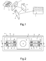
- Figure 1 is a schematic illustration of a picoprojector wherein a light source 1, typically a laser source, generates a light beam 2 (generally formed by three monochromatic beams, one for each base colour), which, through an optical system 3 shown only schematically, is deflected by a pair of MEMS mirrors 5, 6.
- the first MEMS mirror 5 may, for example, be a horizontal micromirror, rotating about a first axis A and generating a fast horizontal scan
- the second MEMS mirror 6 may, for example, be a vertical micromirror, rotating about a second axis B, transverse, in particular perpendicular, to the first axis A, and generating a slow vertical scan, typically of a sawtooth type.
- the combination of the movements of the two MEMS mirrors 5, 6 causes the light beam 2 to perform a complete two-dimensional scanning movement and, once projected on a projection display 7, to generate a two-dimensional image thereon.
- a system is described, for example, in WO 2010/067354 .
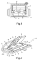
- MEMS mirrors 5, 6 may be formed as shown in Figure 2 .
- a chip 10 comprises a mirror element 11 having a reflecting surface 9 and suspended over a semiconductor substrate 8.
- the mirror element 11 is supported by a pair of arms 12, which extend from opposite sides of the mirror element 11 and define the rotation axis of the mirror element 11 (for example, rotation axis B of the vertical micromirror 6).
- the arms 12 are connected to a fixed peripheral portion 13 of the chip 10, which is fixed with respect to the substrate 8, via torsion springs 14 enabling rotation of the arms 12 about the axis B.
- the arms 12 are further coupled to a driving structure formed by actuation units 18 of an electrostatic type.
- Each actuation unit 18 comprises mobile electrodes 19 facing fixed electrodes 20.
- the mobile electrodes 19 are fixed with respect to the arms 12 and are combfingered with respect to the fixed electrodes 20 for generating a capacitive coupling.
- the fixed electrodes 20 are carried by supporting regions 21, which are generally fixed with respect to the substrate 8 of the chip 10.
- the driving structure is also defined as "comb-drive structure”.
- FIG. 3 shows a mirror group 24 wherein a chip, designated again by 10, is fixedly coupled to a support 25, generally of metal.
- the electric connection lines 27 are connected to the chip 10 via electric wires 28, in a per se known manner.
- FPC flexible printed circuit
- an operator picks up two mirror groups, one for a horizontal MEMS mirror and the other for a vertical MEMS mirror, and using a jig and microactuators in a specific apparatus, positions the two units to mate them, until they are brought into the desired alignment.
- the operator applies a curable glue using ultraviolet light, and the two mirror groups are fixed in the operative position.
- the aim of the present invention is thus to improve the mirror groups for simplifying the assembly operations in electronic apparatuses.
- a mirror group a tape, and a method for assembly of the mirror group are provided, as defined in the attached claims.
- the two micromirrors horizontal and vertical, are assembled on a same metal frame and electrically couple by wire to a respective electric connection element (flexible printed circuit) already fixed to the frame. Then, the frame is bent so as to position the two micromirrors with the desired mutual angular arrangement. Bending may be carried out automatically, without human intervention, using a forming press similar to those used in the semiconductor industry for shaping connection conductors in packages of standard integrated circuits.
- the frame may be carried by a tape, together with a plurality of similar frames, and the individual frames may be separated after a single bending step.
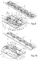
- Figures 4 and 5 show a mirror group 30 designed to be mounted in a portable electronic apparatus (not shown).
- the mirror group 30 comprises a frame 31 of rigid material bent as a V for forming a first supporting portion 32, carrying a first chip 35, and a second supporting portion 32, carrying a second chip 36.
- the frame 31 is in general of sheet metal, typically aluminium, for example with a thickness of about 0.5 mm so as to enable bending thereof in a purposely designed machine (as explained in detail hereinafter) but for have, at the same time, a sufficient stiffness degree to prevent any deformation during handling and a sufficient planarity of the supporting portions 32, 33 for precise positioning the chips 35, 36.
- the first chip 35 is here, for example, a vertical MEMS mirror
- the second chip 36 is here, for example, a horizontal MEMS mirror.
- the chips 35, 36 are fixed to the respective supporting portions 32, 33 via a glue, for example a bi-adhesive layer (so called die attach film), standard in the semiconductor industry.
- a glue for example a bi-adhesive layer (so called die attach film), standard in the semiconductor industry.
- the frame 31 carries two electric connection structures 37, 38, one for each chip 35, 36, formed, for example, as sticky printed circuits, so called FPCs of a known type, embedding electric connection lines (not visible here) similar to the electric connection lines 27 of Figure 3 .
- the electric connection structures 37, 38 are coupled to the chips 35, 36 via wires 60.
- the first supporting portion 32 is connected to the second supporting portion 33 via connection arms 39 having S-shaped bent portions 52, as described in detail below with reference to Figure 8 .
- the frame 31 is obtained via shearing and bending of a plane metal sheet, as described hereinafter with reference to Figures 6-10 .
- the frame 31 is bent about a median virtual line designated by C in Figure 5 so as to obtain a preset angle ⁇ , for example 60°, between the two supporting portions 32, 33, and a preset height H, for example 2.6 mm, between the edge of the second chip 36 which is far with respect to the bending line C and the upper surface of the first chip 35.
- bending determines a deformed area wider than the bending line.
- the median virtual line referred to above will be defined as a bending line C, and the deformed area will be referred to as a bending zone.
- reflecting surfaces 55, 56 of the chips 35, 36 correctly face one another and are in the correct position to be able to deflect a light ray, as in the picoprojector of Figure 1 .
- a tape 40 of sheet metal for example aluminium, is stamped so as to form two strips 41, forming two longitudinal edges of tape 40, and a plurality of frames 31, arranged alongside one another in the longitudinal direction of the tape 40, between the strips 41.
- Each frame 31 has a roughly rectangular shape and is supported by the strips 41 at a plurality of peripheral links 42, here four for each frame 31, arranged at the corners of the roughly rectangular shape, and by supporting arms 43.
- Each supporting arm 43 extends transversely to the strips 41, has ends connected to the two strips 41 and is arranged between two adjacent frames 31.
- each supporting arm 43 is connected to the two adjacent frames 31, arranged on the two sides thereof, via median links 44 that extend between a median portion of the supporting arms 43 and a median portion of the frames 31.
- the median links 44 are formed by S-shaped stretches of metal sheet, arranged in couple symmetrically with respect to the bending axis C so as to define a slit 47 between them, the slit having a longitudinal stretch aligned with the bending axis C.
- each frame 31 the supporting portions 32, 33 are arranged on opposite sides with respect to the bending axis C and are separated from each other by an opening 48 extending in a longitudinal direction of the tape 40, along bending axis C.
- each connection portion comprises a connection arm 49 having a first end connected to the first supporting portion 32 in proximity of a respective outer corner of this first supporting portion 32, close to the strip 41 that is adjacent thereto, and a second end connected to the second supporting portion 33 in proximity of a respective inner corner of the second supporting portion 33, close to bending axis C.
- the median links 44 are connected to the frames 31 at the connection arms 49.
- each connection arm 49 forms a bending zone 49A, as clarified hereinafter, and has an arm portion 49B extending along a transverse side of the respective first supporting portion 32, between the bending zone 49A and the adjacent outer corner of the first supporting portion 32.
- the tape 40 further carries the electric connection elements 37, 38, fixed to the respective supporting portions 32, 33 in a known way.
- the electric connection elements are here U-shaped.
- First alignment holes 50 are formed along the strips 41, and each frame 31 has second alignment holes 51, for example near the ends of the connection arms 49 for coupling to the first supporting portions 32.
- the first and second chips 35, 36 are attached to the respective supporting portions 32, 33 in a known way, for example via a die attach film so as to expose the respective reflecting surfaces 55, 56. Then, in a known way, electric connection wires 60 are soldered for electrically connecting the chips 35, 36 to the respective electric connection elements 37, 38.
- the tape 40 is precut, for removing the peripheral links 42, using a trimming tool (not shown) of a standard type used in packaging integrated circuit, for example for trimming pins of lead-frames.
- a trimming tool (not shown) of a standard type used in packaging integrated circuit, for example for trimming pins of lead-frames.
- each frame 31 is supported by the strips 41 only through the supporting arms 43 and the median links 44.
- connection arms 49 are subjected to a shaping step, using a tool (not shown), of a standard type used in packaging integrated circuits, for example for bending pins of lead-frames, for forming, in each connection arm 49, a respective S-shaped bent portion 52 and arranged along the arm portion 49B, that is thus no longer planar.
- a tool not shown
- a standard type used in packaging integrated circuits for example for bending pins of lead-frames
- a first arm stretch 49B1 connected to the bending zone 49A and a second arm stretch 49B2 connected to the first supporting portion 32 are obtained (see also Figure 4 ). Furthermore, the second arm stretches 49B2 and the first supporting portions 32 connected thereto are no longer co-planar with the rest of the tape 40, in particular with the second supporting portions 33, and the first chips 35 are raised and close to the second chips of the frame 31.
- the frames 31 are bent along the bending line C.
- a shaping press is used for bending the individual frames 31, still fixed to the strips 41 through the supporting arms 43 and the median links 44, so as to bring the two chips 35, 36 into the desired mutual angular and spatial position.
- bending is simplified by the fact that the bending zone of the frames 31 is formed only by the connection arms 49, having a width (in the longitudinal direction of the tape 40) smaller than the respective frames 31, by virtue of the presence of the openings 48 and the slits 47.
- the median links 44 undergo deformation, by twisting, by virtue of their small section. In this way, bending along the bending line C is obtained easily, without any risk of incorrect bending in other parts of the frames 31.
- the individual frames 31 are separated, by cutting the median links 44 in proximity of the connection arms 49, to obtain a plurality of mirror groups 30, shown in Figures 4 and 5 . These may then be dispatched for their final assembly and easily and automatically mounted, also due to the presence of the second alignment holes 51, without requiring complex and delicate operations of manual assembly.
- the horizontal micromirror and the vertical micromirror may be supplied already complete with the horizontal micromirror and the vertical micromirror arranged in the desired mutual angular and spatial position for assembly in electronic apparatuses.
- assembly may be carried out automatically by pick-and-place machines, reducing assembly costs and risks of erroneous positioning, and thus increasing the yield.
- Assembly of the mirror groups in the electronic apparatuses may be carried out using automatic machines, without any human intervention, thus reducing the costs and increasing the productivity.
- the first chip 35 may be brought spatially very close to the second chip 36, for a same bending angle ⁇ , thus reducing the dimensions of the corresponding first supporting portion 32.
- the tape 40 has a smaller width (in the transverse direction), enabling a reduction of material and of storage space, and thus a reduction of the associated costs.
- the bending lines C could be transverse instead of longitudinal, and the first and second supporting portions 32, 33 of each frame 31 could be longitudinally aligned with respect to the tape 40.
Landscapes
- Physics & Mathematics (AREA)
- Engineering & Computer Science (AREA)
- General Physics & Mathematics (AREA)
- Optics & Photonics (AREA)
- Microelectronics & Electronic Packaging (AREA)
- Manufacturing & Machinery (AREA)
- Computer Hardware Design (AREA)
- Micromachines (AREA)
- Mechanical Light Control Or Optical Switches (AREA)
Abstract
Description
- The present invention relates to a mirror group, in particular for a picoprojector, comprising micromirrors obtained using the MEMS technology.
- As is known, picoprojectors are devices of small dimensions which are able to project, on a wall or other surface, images, video clips, and other visual documents stored in small portable electronic equipment, such as cellphones, tablets, laptops, and the like. Furthermore, it has already been proposed to integrate such picoprojectors on the dashboard of motor vehicles, for example for projecting onto the windscreen information on satellite-navigation functions and other route or communication information.
- In order to reduce the size, picoprojectors use MEMS micromirror systems, which are able to turn about two axes in order to perform a movement of scanning of a two-dimensional area. In particular, in some solutions, micromirror systems comprise a pair of MEMS mirrors driven for turning about two mutually perpendicular rotation axes.
- For instance,
Figure 1 is a schematic illustration of a picoprojector wherein a light source 1, typically a laser source, generates a light beam 2 (generally formed by three monochromatic beams, one for each base colour), which, through anoptical system 3 shown only schematically, is deflected by a pair ofMEMS mirrors first MEMS mirror 5 may, for example, be a horizontal micromirror, rotating about a first axis A and generating a fast horizontal scan, and thesecond MEMS mirror 6 may, for example, be a vertical micromirror, rotating about a second axis B, transverse, in particular perpendicular, to the first axis A, and generating a slow vertical scan, typically of a sawtooth type. The combination of the movements of the twoMEMS mirrors light beam 2 to perform a complete two-dimensional scanning movement and, once projected on aprojection display 7, to generate a two-dimensional image thereon. Such a system is described, for example, inWO 2010/067354 . -
MEMS mirrors Figure 2 . Here, achip 10 comprises amirror element 11 having a reflectingsurface 9 and suspended over asemiconductor substrate 8. Themirror element 11 is supported by a pair ofarms 12, which extend from opposite sides of themirror element 11 and define the rotation axis of the mirror element 11 (for example, rotation axis B of the vertical micromirror 6). Thearms 12 are connected to a fixedperipheral portion 13 of thechip 10, which is fixed with respect to thesubstrate 8, viatorsion springs 14 enabling rotation of thearms 12 about the axis B. Thearms 12 are further coupled to a driving structure formed byactuation units 18 of an electrostatic type. Eachactuation unit 18 comprisesmobile electrodes 19 facingfixed electrodes 20. - In detail, the
mobile electrodes 19 are fixed with respect to thearms 12 and are combfingered with respect to thefixed electrodes 20 for generating a capacitive coupling. Thefixed electrodes 20 are carried by supportingregions 21, which are generally fixed with respect to thesubstrate 8 of thechip 10. By virtue of the arrangement of theelectrodes - By applying appropriate voltages between the
mobile electrodes 19 and thefixed electrodes 20, it is possible to generate attraction/repulsion forces between them and cause rotation of themobile electrodes 19 with respect to thefixed electrodes 20, rotation of thearms 12 about axis B, and thus the corresponding controlled rotation of themirror element 11. - Currently,
MEMS mirrors Figure 3 shows a mirror group 24 wherein a chip, designated again by 10, is fixedly coupled to asupport 25, generally of metal. Anelectric connection structure 26, for example a flexible printed circuit (FPC) carryingelectric connection lines 27, is also fixedly coupled to thesupport 25. Theelectric connection lines 27 are connected to thechip 10 viaelectric wires 28, in a per se known manner. - During assembly in a portable electronic apparatus, an operator picks up two mirror groups, one for a horizontal MEMS mirror and the other for a vertical MEMS mirror, and using a jig and microactuators in a specific apparatus, positions the two units to mate them, until they are brought into the desired alignment. Next, the operator applies a curable glue using ultraviolet light, and the two mirror groups are fixed in the operative position.
- This type of assembly is slow, difficult, and sensibly error-prone. It follows that, with this method, the throughput and yield of correctly mounted pieces are not optimal.
- The aim of the present invention is thus to improve the mirror groups for simplifying the assembly operations in electronic apparatuses.
- According to the present invention, a mirror group, a tape, and a method for assembly of the mirror group are provided, as defined in the attached claims.
- In one embodiment, the two micromirrors, horizontal and vertical, are assembled on a same metal frame and electrically couple by wire to a respective electric connection element (flexible printed circuit) already fixed to the frame. Then, the frame is bent so as to position the two micromirrors with the desired mutual angular arrangement. Bending may be carried out automatically, without human intervention, using a forming press similar to those used in the semiconductor industry for shaping connection conductors in packages of standard integrated circuits. The frame may be carried by a tape, together with a plurality of similar frames, and the individual frames may be separated after a single bending step.
- For a better understanding of the present invention, preferred embodiments thereof are now described, purely by way of non-limiting example, with reference to the attached drawings, wherein:
-
Figure 1 is a schematic perspective view of a picoprojector; -
Figure 2 is a schematic illustration of an embodiment of a micromirror ofFigure 1 ; -
Figure 3 is a top plan view of a micromirror mounted on a support prior to assembly in an electronic apparatus; -
Figure 4 is a perspective view of the present mirror group; -
Figures 5 is a side view of the mirror group ofFigure 4 ; and -
Figures 6-10 show, in perspective view, a tape comprising a plurality of frames for manufacturing micromirror groups in successive assembly steps. -
Figures 4 and5 show amirror group 30 designed to be mounted in a portable electronic apparatus (not shown). - The
mirror group 30 comprises aframe 31 of rigid material bent as a V for forming a first supportingportion 32, carrying afirst chip 35, and a second supportingportion 32, carrying asecond chip 36. - The
frame 31 is in general of sheet metal, typically aluminium, for example with a thickness of about 0.5 mm so as to enable bending thereof in a purposely designed machine (as explained in detail hereinafter) but for have, at the same time, a sufficient stiffness degree to prevent any deformation during handling and a sufficient planarity of the supportingportions chips - The
first chip 35 is here, for example, a vertical MEMS mirror, and thesecond chip 36 is here, for example, a horizontal MEMS mirror. Thechips portions - Furthermore, the
frame 31 carries twoelectric connection structures chip electric connection lines 27 ofFigure 3 . Theelectric connection structures chips wires 60. - The first supporting
portion 32 is connected to the second supportingportion 33 via connection arms 39 having S-shaped bent portions 52, as described in detail below with reference toFigure 8 . - The
frame 31 is obtained via shearing and bending of a plane metal sheet, as described hereinafter with reference toFigures 6-10 . In particular, theframe 31 is bent about a median virtual line designated by C inFigure 5 so as to obtain a preset angle α, for example 60°, between the two supportingportions second chip 36 which is far with respect to the bending line C and the upper surface of thefirst chip 35. In fact, bending determines a deformed area wider than the bending line. For simplicity, in the following, the median virtual line referred to above will be defined as a bending line C, and the deformed area will be referred to as a bending zone. - In this way, reflecting
surfaces chips Figure 1 . - With reference to
Figure 6 , atape 40 of sheet metal, for example aluminium, is stamped so as to form twostrips 41, forming two longitudinal edges oftape 40, and a plurality offrames 31, arranged alongside one another in the longitudinal direction of thetape 40, between thestrips 41. Eachframe 31 has a roughly rectangular shape and is supported by thestrips 41 at a plurality ofperipheral links 42, here four for eachframe 31, arranged at the corners of the roughly rectangular shape, and by supportingarms 43. Each supportingarm 43 extends transversely to thestrips 41, has ends connected to the twostrips 41 and is arranged between twoadjacent frames 31. In addition, each supportingarm 43 is connected to the twoadjacent frames 31, arranged on the two sides thereof, viamedian links 44 that extend between a median portion of the supportingarms 43 and a median portion of theframes 31. - In detail, the
median links 44 are formed by S-shaped stretches of metal sheet, arranged in couple symmetrically with respect to the bending axis C so as to define aslit 47 between them, the slit having a longitudinal stretch aligned with the bending axis C. - In each
frame 31, the supportingportions tape 40, along bending axis C. - The supporting
portions frame 31 have a generally rectangular shape and are connected to one another via connection portions, extending transversely with respect to thetape 40 and across the bending line C. In the embodiment shown, each connection portion comprises aconnection arm 49 having a first end connected to the first supportingportion 32 in proximity of a respective outer corner of this first supportingportion 32, close to thestrip 41 that is adjacent thereto, and a second end connected to the second supportingportion 33 in proximity of a respective inner corner of the second supportingportion 33, close to bending axis C. Themedian links 44 are connected to theframes 31 at theconnection arms 49. - In this way, each
connection arm 49 forms abending zone 49A, as clarified hereinafter, and has anarm portion 49B extending along a transverse side of the respective first supportingportion 32, between thebending zone 49A and the adjacent outer corner of the first supportingportion 32. - The
tape 40 further carries theelectric connection elements portions -
First alignment holes 50 are formed along thestrips 41, and eachframe 31 hassecond alignment holes 51, for example near the ends of theconnection arms 49 for coupling to the first supportingportions 32. - In
Figure 7 , the first andsecond chips portions surfaces electric connection wires 60 are soldered for electrically connecting thechips electric connection elements - Next,
Figure 8 , thetape 40 is precut, for removing theperipheral links 42, using a trimming tool (not shown) of a standard type used in packaging integrated circuit, for example for trimming pins of lead-frames. In this way, eachframe 31 is supported by thestrips 41 only through the supportingarms 43 and themedian links 44. - Then,
Figure 9 , thestretches 49B of all theconnection arms 49 are subjected to a shaping step, using a tool (not shown), of a standard type used in packaging integrated circuits, for example for bending pins of lead-frames, for forming, in eachconnection arm 49, a respective S-shapedbent portion 52 and arranged along thearm portion 49B, that is thus no longer planar. - In particular, in this way, a first arm stretch 49B1 connected to the
bending zone 49A and a second arm stretch 49B2 connected to the first supportingportion 32 are obtained (see alsoFigure 4 ). Furthermore, the second arm stretches 49B2 and the first supportingportions 32 connected thereto are no longer co-planar with the rest of thetape 40, in particular with the second supportingportions 33, and thefirst chips 35 are raised and close to the second chips of theframe 31. - Next,
Figure 10 , theframes 31 are bent along the bending line C. To this end, a shaping press is used for bending the individual frames 31, still fixed to thestrips 41 through the supportingarms 43 and themedian links 44, so as to bring the twochips frames 31 is formed only by theconnection arms 49, having a width (in the longitudinal direction of the tape 40) smaller than therespective frames 31, by virtue of the presence of theopenings 48 and theslits 47. In this step, themedian links 44 undergo deformation, by twisting, by virtue of their small section. In this way, bending along the bending line C is obtained easily, without any risk of incorrect bending in other parts of theframes 31. - Finally, the individual frames 31 are separated, by cutting the
median links 44 in proximity of theconnection arms 49, to obtain a plurality ofmirror groups 30, shown inFigures 4 and5 . These may then be dispatched for their final assembly and easily and automatically mounted, also due to the presence of the second alignment holes 51, without requiring complex and delicate operations of manual assembly. - The mirror groups described herein have numerous advantages.
- In particular, they may be supplied already complete with the horizontal micromirror and the vertical micromirror arranged in the desired mutual angular and spatial position for assembly in electronic apparatuses. In this way, assembly may be carried out automatically by pick-and-place machines, reducing assembly costs and risks of erroneous positioning, and thus increasing the yield.
- Assembly of the mirror groups in the electronic apparatuses may be carried out using automatic machines, without any human intervention, thus reducing the costs and increasing the productivity.
- Due to the S-shaped
bent portion 52 of theconnection arms 49, thefirst chip 35 may be brought spatially very close to thesecond chip 36, for a same bending angle α, thus reducing the dimensions of the corresponding first supportingportion 32. In this way, thetape 40 has a smaller width (in the transverse direction), enabling a reduction of material and of storage space, and thus a reduction of the associated costs. - Finally, it is clear that modifications and variations may be made to the mirror group, to the tape, and to the assembling method described and illustrated herein, without thereby departing from the scope of the present invention, as defined in the attached claims.
- For instance, the bending lines C could be transverse instead of longitudinal, and the first and second supporting
portions frame 31 could be longitudinally aligned with respect to thetape 40.
Claims (15)
- A mirror group (30) comprising:a first chip (35) of semiconductor material, forming a first micromirror;a second chip (36) of semiconductor material, forming a second micromirror; anda frame (31), being monolithic, bent along a bending line (C) and including a first supporting portion (32) and a second supporting portion (33) carrying, respectively, the first and second chips, the first and second supporting portions (32, 33) being arranged on opposite sides of the bending line (C) of the frame and being arranged angularly inclined with respect to each other.
- A mirror group according to claim 1, wherein the first and second supporting portions (32, 33) have a polygonal shape and are connected to each other by a pair of connection portions (49) having a bending zone (49A) along the bending line (C).
- A mirror group according to claim 2, wherein the first and second supporting portions (32, 33) have a generally rectangular shape.
- A mirror group according to claim 2 or 3, wherein the connection portions (49) each comprise a connection arm having a first end fixedly coupled to the first supporting portion (32) and a second end fixedly coupled to the second supporting portion (33).
- A mirror group according to claim 4, wherein the connection arms (49) each have an S-shaped bent portion (52) arranged between the bending zone (49A) and the first end and defining a first arm stretch (49B1) connected to the bending zone (49A) and a second arm stretch (49B2) connected to the first supporting portion (32), the first supporting portion and the second arm stretch (49B2) being not co-planar with respect to the first stretch (49B1) of the connection arms (49).
- A mirror group according to claim 4 or 5, comprising an opening (48) extending between the first and second supporting portions (32, 33) along the bending line (C).
- A mirror group according to any of the preceding claims, wherein the first and second supporting portions (32, 33) each carry a respective flexible electric connection element (37, 38), coupled, respectively, to the first and second chips (35, 36).
- A sheet metal tape (40) for assembly of integrated micromirrors, comprising:a pair of longitudinal strips (41), extending parallel to each other at a distance;a plurality of frames (31), extending alongside each other between the longitudinal strips; andperipheral link elements (42), arranged between the longitudinal strips (41) and the frames (31),wherein each frame (31) of the plurality of frames is monolithic with the longitudinal strips (41) and the peripheral link elements (42) and has a first and a second supporting portion (32, 33) for respective integrated micromirror chips (35, 36), the first and second supporting portions (32, 33) being arranged on opposite sides of a bending line (C) of the frame.
- A sheet metal tape according to claim 8, further comprising a plurality of supporting arms (43) and a plurality of median link elements (44), each supporting arm (43) being monolithic with the frames (31), extending in a transverse direction with respect to the longitudinal strips (41), having ends fixedly coupled to the longitudinal strips, and arranged between two adjacent frames (31) of the plurality of frames; and each median link element (44) being arranged between a supporting arm (43) and an adjacent frame (31) of the plurality of frames.
- A sheet metal tape according to claim 9, wherein the median link elements (44) are arranged in pairs on two opposite sides of the bending line (C) of each frame (31) and form longitudinal slits (47) aligned to the bending line, and the first and second supporting portions (32, 33) of each frame (31) are separated from each other by a respective opening (48) extending between the first and second supporting portions of each frame (31) along the bending line (C).
- A method for assembling a mirror group comprising:fixing a first chip (35) of semiconductor material integrating a first micromirror to a first supporting portion (32) of a frame (31);fixing a second chip (36) of semiconductor material integrating a second micromirror to a second supporting portion (33) of the frame; andbending the frame (31) along a bending line (C) so that the first and second supporting portions are arranged angularly inclined with respect to one another.
- An assembling method according to claim 11, wherein the step of bending of the frame (31) is carried out in a press.
- An assembling method according to claim 11 or 12, wherein the frame (31) has a pair of connection arms (49) having a first end fixedly coupled to the first supporting portion (32) and a second end fixedly coupled to the second supporting portion (33), the method comprising the step of bending the connection arms (49) in an area arranged between the bending line (C) and the first end, and forming an S-shaped bent portion (52).
- An assembling method according to any one of claims 11-13, wherein the frame (31) is a frame of a plurality of adjacent frames carried by a pair of longitudinal strips (41) extending parallel to one another, the method comprising the step of bending the plurality of frames (31) along respective bending lines (C) and separating the frames (31) from the longitudinal strips (41) and from each other.
- An assembling method according to any of claims 11-14, wherein the frame (31) carries flexible electric connection elements (37, 38), the method comprising the step of electrically connecting the first and second chips to the flexible electric connection elements via electric wires (60) prior to bending the frame (31).
Applications Claiming Priority (1)
| Application Number | Priority Date | Filing Date | Title |
|---|---|---|---|
| ITUB2016A000719A ITUB20160719A1 (en) | 2016-02-12 | 2016-02-12 | MIRROR GROUP, IN PARTICULAR FOR PICOPROJECTOR, INCLUDING MICROSPECTS MADE IN MEMS TECHNOLOGY |
Publications (2)
| Publication Number | Publication Date |
|---|---|
| EP3206071A1 true EP3206071A1 (en) | 2017-08-16 |
| EP3206071B1 EP3206071B1 (en) | 2018-09-19 |
Family
ID=55806706
Family Applications (1)
| Application Number | Title | Priority Date | Filing Date |
|---|---|---|---|
| EP16194664.5A Active EP3206071B1 (en) | 2016-02-12 | 2016-10-19 | Mirror group, in particular for a picoprojector, comprising micromirrors made using the mems technology |
Country Status (4)
| Country | Link |
|---|---|
| US (1) | US10338378B2 (en) |
| EP (1) | EP3206071B1 (en) |
| CN (2) | CN206441727U (en) |
| IT (1) | ITUB20160719A1 (en) |
Cited By (1)
| Publication number | Priority date | Publication date | Assignee | Title |
|---|---|---|---|---|
| IT202000022715A1 (en) | 2020-09-25 | 2022-03-25 | St Microelectronics Srl | INTEGRATED ELECTRONIC MODULE INCLUDING TWO MICROMIRRORS, AND SYSTEM THAT INCLUDE THE ELECTRONIC MODULE |
Families Citing this family (8)
| Publication number | Priority date | Publication date | Assignee | Title |
|---|---|---|---|---|
| ITUB20160719A1 (en) * | 2016-02-12 | 2017-08-12 | St Microelectronics Srl | MIRROR GROUP, IN PARTICULAR FOR PICOPROJECTOR, INCLUDING MICROSPECTS MADE IN MEMS TECHNOLOGY |
| EP3214480B1 (en) * | 2016-03-01 | 2018-11-28 | Funai Electric Co., Ltd. | Oscillating mirror element |
| US10237515B2 (en) * | 2017-03-28 | 2019-03-19 | Stmicroelectronics Ltd | MEMS projector using multiple laser sources |
| CN107966810A (en) * | 2017-12-19 | 2018-04-27 | 无锡英菲感知技术有限公司 | A kind of two-dimensional scanning micro mirror |
| CN113031287A (en) * | 2019-12-09 | 2021-06-25 | 觉芯电子(无锡)有限公司 | Optical integrator, speckle suppression device and laser display system thereof |
| CN113031256B (en) * | 2019-12-09 | 2023-05-09 | 觉芯电子(无锡)有限公司 | Micro-mirror integrating lens array, micro-mirror preparation method and laser display system |
| CN113805409A (en) | 2020-05-29 | 2021-12-17 | 英錡科技股份有限公司 | Projection device |
| CN114252989A (en) * | 2020-09-25 | 2022-03-29 | 意法半导体股份有限公司 | Integrated electronic module comprising two micromirrors and system comprising an electronic module |
Citations (5)
| Publication number | Priority date | Publication date | Assignee | Title |
|---|---|---|---|---|
| US20040252501A1 (en) * | 2002-04-24 | 2004-12-16 | Hideo Moriyama | Light source coupler, illuminant device, patterned conductor, and method for manufacturing light source coupler |
| US20050013534A1 (en) * | 2003-07-14 | 2005-01-20 | Atsushi Kazama | Beam direction module and optical switch using the same |
| US20090190201A1 (en) * | 2008-01-30 | 2009-07-30 | Olympus Corporation | Micromirror device |
| WO2010067354A1 (en) | 2008-12-14 | 2010-06-17 | Btendo Ltd. | Device and method for scanning images by laser projector |
| DE102014208498A1 (en) * | 2014-05-07 | 2015-11-12 | Robert Bosch Gmbh | Mounting body for micromirror chips, mirror device and manufacturing method for a mirror device |
Family Cites Families (10)
| Publication number | Priority date | Publication date | Assignee | Title |
|---|---|---|---|---|
| DE10240598A1 (en) | 2002-08-27 | 2004-03-25 | Carl Zeiss Smt Ag | Catadioptric reflective/reduction lens for mapping an image pattern transfers a picture of the pattern in an object plane into an image plane |
| US6906848B2 (en) * | 2003-02-24 | 2005-06-14 | Exajoule, Llc | Micromirror systems with concealed multi-piece hinge structures |
| TWI225246B (en) | 2003-05-21 | 2004-12-11 | Fan-Gang Tseng | Micro optical pickup head module, method of manufacturing the same and method of manufacturing the objective lens of the same |
| JP4680833B2 (en) | 2006-05-23 | 2011-05-11 | 株式会社東海理化電機製作所 | Connector and mirror surface angle adjusting device |
| CA2624400A1 (en) | 2007-06-21 | 2008-12-21 | Jds Uniphase Corporation | Mems device with an angular vertical comb actuator |
| CN101532880B (en) | 2008-03-12 | 2010-12-15 | 中国科学院西安光学精密机械研究所 | Double moving mirror interferometer |
| JP2011123245A (en) | 2009-12-10 | 2011-06-23 | Panasonic Corp | Optical reflecting element |
| JP2013190448A (en) | 2010-06-30 | 2013-09-26 | Sharp Corp | Display device |
| JP2014142517A (en) | 2013-01-24 | 2014-08-07 | Funai Electric Co Ltd | Oscillation mirror element and electronic apparatus having projector function |
| ITUB20160719A1 (en) * | 2016-02-12 | 2017-08-12 | St Microelectronics Srl | MIRROR GROUP, IN PARTICULAR FOR PICOPROJECTOR, INCLUDING MICROSPECTS MADE IN MEMS TECHNOLOGY |
-
2016
- 2016-02-12 IT ITUB2016A000719A patent/ITUB20160719A1/en unknown
- 2016-09-13 US US15/264,446 patent/US10338378B2/en active Active
- 2016-09-30 CN CN201621102197.0U patent/CN206441727U/en not_active Withdrawn - After Issue
- 2016-09-30 CN CN201610875917.5A patent/CN107082406B/en active Active
- 2016-10-19 EP EP16194664.5A patent/EP3206071B1/en active Active
Patent Citations (5)
| Publication number | Priority date | Publication date | Assignee | Title |
|---|---|---|---|---|
| US20040252501A1 (en) * | 2002-04-24 | 2004-12-16 | Hideo Moriyama | Light source coupler, illuminant device, patterned conductor, and method for manufacturing light source coupler |
| US20050013534A1 (en) * | 2003-07-14 | 2005-01-20 | Atsushi Kazama | Beam direction module and optical switch using the same |
| US20090190201A1 (en) * | 2008-01-30 | 2009-07-30 | Olympus Corporation | Micromirror device |
| WO2010067354A1 (en) | 2008-12-14 | 2010-06-17 | Btendo Ltd. | Device and method for scanning images by laser projector |
| DE102014208498A1 (en) * | 2014-05-07 | 2015-11-12 | Robert Bosch Gmbh | Mounting body for micromirror chips, mirror device and manufacturing method for a mirror device |
Cited By (3)
| Publication number | Priority date | Publication date | Assignee | Title |
|---|---|---|---|---|
| IT202000022715A1 (en) | 2020-09-25 | 2022-03-25 | St Microelectronics Srl | INTEGRATED ELECTRONIC MODULE INCLUDING TWO MICROMIRRORS, AND SYSTEM THAT INCLUDE THE ELECTRONIC MODULE |
| EP3974889A1 (en) | 2020-09-25 | 2022-03-30 | STMicroelectronics S.r.l. | Integrated electronic module including two micromirrors, and system including the electronic module |
| US12204092B2 (en) | 2020-09-25 | 2025-01-21 | Stmicroelectronics S.R.L. | Integrated electronic module including two micromirrors, and system including the electronic module |
Also Published As
| Publication number | Publication date |
|---|---|
| ITUB20160719A1 (en) | 2017-08-12 |
| CN107082406A (en) | 2017-08-22 |
| US10338378B2 (en) | 2019-07-02 |
| CN107082406B (en) | 2019-05-28 |
| US20170235128A1 (en) | 2017-08-17 |
| EP3206071B1 (en) | 2018-09-19 |
| CN206441727U (en) | 2017-08-25 |
Similar Documents
| Publication | Publication Date | Title |
|---|---|---|
| EP3206071B1 (en) | Mirror group, in particular for a picoprojector, comprising micromirrors made using the mems technology | |
| US9323047B2 (en) | Method of manufacturing a MEMS micro-mirror assembly | |
| US10175474B2 (en) | Micromechanical device having a structure tiltable by a quasi-static piezoelectric actuation | |
| KR102324264B1 (en) | A pressing jig apparatus that closely contacts electrode lead with bus bar and a battery module manufacturing system comprising the same | |
| JP7225771B2 (en) | Mobile devices, distance measuring devices, image projection devices, vehicles, and pedestals | |
| EP3899636B1 (en) | MOVABLE DEVICE, DISTANCE MEASURING DEVICE AND MOUNTING | |
| US6657764B1 (en) | Very large angle integrated optical scanner made with an array of piezoelectric monomorphs | |
| KR20160088514A (en) | Manufacturing method for backlight unit of curved display apparatus | |
| US11125969B2 (en) | Bonding of resonant oscillating mirror to frame | |
| EP3064975B1 (en) | Optical scanning apparatus, substrate fixing method in optical scanning apparatus, image display apparatus, and vehicle | |
| EP1798585A2 (en) | Two-axis scanner | |
| JP6233396B2 (en) | Optical scanning device | |
| CN205767920U (en) | Carrier for laminating | |
| CN223168627U (en) | Die transfer equipment | |
| CN112748567B (en) | Vertically displaced electrostatic actuator and optical scanner using the same | |
| US12001105B2 (en) | System and method for the right-sizing of LCD screens, screens adapted for dividing into a plurality of custom sized screens, and right-sized screens derived therefrom | |
| KR100485127B1 (en) | Design for Micromirror Structure and Micromirror Arrays | |
| TW202510158A (en) | Die transfer device | |
| CN105818511A (en) | Carrier for attaching and application of carrier | |
| JPH10268325A (en) | Method and apparatus for assembling flat panel display | |
| JPH04318811A (en) | Electrooptical element and method for packaging electrooptical element | |
| JP2009300736A (en) | Method of manufacturing optical scanner |
Legal Events
| Date | Code | Title | Description |
|---|---|---|---|
| PUAI | Public reference made under article 153(3) epc to a published international application that has entered the european phase |
Free format text: ORIGINAL CODE: 0009012 |
|
| AK | Designated contracting states |
Kind code of ref document: A1 Designated state(s): AL AT BE BG CH CY CZ DE DK EE ES FI FR GB GR HR HU IE IS IT LI LT LU LV MC MK MT NL NO PL PT RO RS SE SI SK SM TR |
|
| AX | Request for extension of the european patent |
Extension state: BA ME |
|
| 17P | Request for examination filed |
Effective date: 20180212 |
|
| RBV | Designated contracting states (corrected) |
Designated state(s): AL AT BE BG CH CY CZ DE DK EE ES FI FR GB GR HR HU IE IS IT LI LT LU LV MC MK MT NL NO PL PT RO RS SE SI SK SM TR |
|
| GRAP | Despatch of communication of intention to grant a patent |
Free format text: ORIGINAL CODE: EPIDOSNIGR1 |
|
| INTG | Intention to grant announced |
Effective date: 20180403 |
|
| GRAS | Grant fee paid |
Free format text: ORIGINAL CODE: EPIDOSNIGR3 |
|
| GRAA | (expected) grant |
Free format text: ORIGINAL CODE: 0009210 |
|
| AK | Designated contracting states |
Kind code of ref document: B1 Designated state(s): AL AT BE BG CH CY CZ DE DK EE ES FI FR GB GR HR HU IE IS IT LI LT LU LV MC MK MT NL NO PL PT RO RS SE SI SK SM TR |
|
| REG | Reference to a national code |
Ref country code: GB Ref legal event code: FG4D |
|
| REG | Reference to a national code |
Ref country code: CH Ref legal event code: EP |
|
| REG | Reference to a national code |
Ref country code: AT Ref legal event code: REF Ref document number: 1043921 Country of ref document: AT Kind code of ref document: T Effective date: 20181015 |
|
| REG | Reference to a national code |
Ref country code: IE Ref legal event code: FG4D |
|
| REG | Reference to a national code |
Ref country code: DE Ref legal event code: R096 Ref document number: 602016005716 Country of ref document: DE |
|
| REG | Reference to a national code |
Ref country code: NL Ref legal event code: MP Effective date: 20180919 |
|
| PG25 | Lapsed in a contracting state [announced via postgrant information from national office to epo] |
Ref country code: NO Free format text: LAPSE BECAUSE OF FAILURE TO SUBMIT A TRANSLATION OF THE DESCRIPTION OR TO PAY THE FEE WITHIN THE PRESCRIBED TIME-LIMIT Effective date: 20181219 Ref country code: BG Free format text: LAPSE BECAUSE OF FAILURE TO SUBMIT A TRANSLATION OF THE DESCRIPTION OR TO PAY THE FEE WITHIN THE PRESCRIBED TIME-LIMIT Effective date: 20181219 Ref country code: GR Free format text: LAPSE BECAUSE OF FAILURE TO SUBMIT A TRANSLATION OF THE DESCRIPTION OR TO PAY THE FEE WITHIN THE PRESCRIBED TIME-LIMIT Effective date: 20181220 Ref country code: FI Free format text: LAPSE BECAUSE OF FAILURE TO SUBMIT A TRANSLATION OF THE DESCRIPTION OR TO PAY THE FEE WITHIN THE PRESCRIBED TIME-LIMIT Effective date: 20180919 Ref country code: RS Free format text: LAPSE BECAUSE OF FAILURE TO SUBMIT A TRANSLATION OF THE DESCRIPTION OR TO PAY THE FEE WITHIN THE PRESCRIBED TIME-LIMIT Effective date: 20180919 Ref country code: LT Free format text: LAPSE BECAUSE OF FAILURE TO SUBMIT A TRANSLATION OF THE DESCRIPTION OR TO PAY THE FEE WITHIN THE PRESCRIBED TIME-LIMIT Effective date: 20180919 Ref country code: SE Free format text: LAPSE BECAUSE OF FAILURE TO SUBMIT A TRANSLATION OF THE DESCRIPTION OR TO PAY THE FEE WITHIN THE PRESCRIBED TIME-LIMIT Effective date: 20180919 |
|
| REG | Reference to a national code |
Ref country code: LT Ref legal event code: MG4D |
|
| PG25 | Lapsed in a contracting state [announced via postgrant information from national office to epo] |
Ref country code: AL Free format text: LAPSE BECAUSE OF FAILURE TO SUBMIT A TRANSLATION OF THE DESCRIPTION OR TO PAY THE FEE WITHIN THE PRESCRIBED TIME-LIMIT Effective date: 20180919 Ref country code: HR Free format text: LAPSE BECAUSE OF FAILURE TO SUBMIT A TRANSLATION OF THE DESCRIPTION OR TO PAY THE FEE WITHIN THE PRESCRIBED TIME-LIMIT Effective date: 20180919 Ref country code: LV Free format text: LAPSE BECAUSE OF FAILURE TO SUBMIT A TRANSLATION OF THE DESCRIPTION OR TO PAY THE FEE WITHIN THE PRESCRIBED TIME-LIMIT Effective date: 20180919 |
|
| REG | Reference to a national code |
Ref country code: AT Ref legal event code: MK05 Ref document number: 1043921 Country of ref document: AT Kind code of ref document: T Effective date: 20180919 |
|
| PG25 | Lapsed in a contracting state [announced via postgrant information from national office to epo] |
Ref country code: NL Free format text: LAPSE BECAUSE OF FAILURE TO SUBMIT A TRANSLATION OF THE DESCRIPTION OR TO PAY THE FEE WITHIN THE PRESCRIBED TIME-LIMIT Effective date: 20180919 Ref country code: EE Free format text: LAPSE BECAUSE OF FAILURE TO SUBMIT A TRANSLATION OF THE DESCRIPTION OR TO PAY THE FEE WITHIN THE PRESCRIBED TIME-LIMIT Effective date: 20180919 Ref country code: AT Free format text: LAPSE BECAUSE OF FAILURE TO SUBMIT A TRANSLATION OF THE DESCRIPTION OR TO PAY THE FEE WITHIN THE PRESCRIBED TIME-LIMIT Effective date: 20180919 Ref country code: IS Free format text: LAPSE BECAUSE OF FAILURE TO SUBMIT A TRANSLATION OF THE DESCRIPTION OR TO PAY THE FEE WITHIN THE PRESCRIBED TIME-LIMIT Effective date: 20190119 Ref country code: PL Free format text: LAPSE BECAUSE OF FAILURE TO SUBMIT A TRANSLATION OF THE DESCRIPTION OR TO PAY THE FEE WITHIN THE PRESCRIBED TIME-LIMIT Effective date: 20180919 Ref country code: CZ Free format text: LAPSE BECAUSE OF FAILURE TO SUBMIT A TRANSLATION OF THE DESCRIPTION OR TO PAY THE FEE WITHIN THE PRESCRIBED TIME-LIMIT Effective date: 20180919 Ref country code: IT Free format text: LAPSE BECAUSE OF FAILURE TO SUBMIT A TRANSLATION OF THE DESCRIPTION OR TO PAY THE FEE WITHIN THE PRESCRIBED TIME-LIMIT Effective date: 20180919 Ref country code: ES Free format text: LAPSE BECAUSE OF FAILURE TO SUBMIT A TRANSLATION OF THE DESCRIPTION OR TO PAY THE FEE WITHIN THE PRESCRIBED TIME-LIMIT Effective date: 20180919 Ref country code: RO Free format text: LAPSE BECAUSE OF FAILURE TO SUBMIT A TRANSLATION OF THE DESCRIPTION OR TO PAY THE FEE WITHIN THE PRESCRIBED TIME-LIMIT Effective date: 20180919 |
|
| PG25 | Lapsed in a contracting state [announced via postgrant information from national office to epo] |
Ref country code: SM Free format text: LAPSE BECAUSE OF FAILURE TO SUBMIT A TRANSLATION OF THE DESCRIPTION OR TO PAY THE FEE WITHIN THE PRESCRIBED TIME-LIMIT Effective date: 20180919 Ref country code: PT Free format text: LAPSE BECAUSE OF FAILURE TO SUBMIT A TRANSLATION OF THE DESCRIPTION OR TO PAY THE FEE WITHIN THE PRESCRIBED TIME-LIMIT Effective date: 20190119 Ref country code: SK Free format text: LAPSE BECAUSE OF FAILURE TO SUBMIT A TRANSLATION OF THE DESCRIPTION OR TO PAY THE FEE WITHIN THE PRESCRIBED TIME-LIMIT Effective date: 20180919 |
|
| REG | Reference to a national code |
Ref country code: DE Ref legal event code: R097 Ref document number: 602016005716 Country of ref document: DE |
|
| REG | Reference to a national code |
Ref country code: BE Ref legal event code: MM Effective date: 20181031 |
|
| PG25 | Lapsed in a contracting state [announced via postgrant information from national office to epo] |
Ref country code: LU Free format text: LAPSE BECAUSE OF NON-PAYMENT OF DUE FEES Effective date: 20181019 |
|
| REG | Reference to a national code |
Ref country code: IE Ref legal event code: MM4A |
|
| PLBE | No opposition filed within time limit |
Free format text: ORIGINAL CODE: 0009261 |
|
| STAA | Information on the status of an ep patent application or granted ep patent |
Free format text: STATUS: NO OPPOSITION FILED WITHIN TIME LIMIT |
|
| PG25 | Lapsed in a contracting state [announced via postgrant information from national office to epo] |
Ref country code: DK Free format text: LAPSE BECAUSE OF FAILURE TO SUBMIT A TRANSLATION OF THE DESCRIPTION OR TO PAY THE FEE WITHIN THE PRESCRIBED TIME-LIMIT Effective date: 20180919 Ref country code: MC Free format text: LAPSE BECAUSE OF FAILURE TO SUBMIT A TRANSLATION OF THE DESCRIPTION OR TO PAY THE FEE WITHIN THE PRESCRIBED TIME-LIMIT Effective date: 20180919 |
|
| 26N | No opposition filed |
Effective date: 20190620 |
|
| PG25 | Lapsed in a contracting state [announced via postgrant information from national office to epo] |
Ref country code: BE Free format text: LAPSE BECAUSE OF NON-PAYMENT OF DUE FEES Effective date: 20181031 |
|
| PG25 | Lapsed in a contracting state [announced via postgrant information from national office to epo] |
Ref country code: SI Free format text: LAPSE BECAUSE OF FAILURE TO SUBMIT A TRANSLATION OF THE DESCRIPTION OR TO PAY THE FEE WITHIN THE PRESCRIBED TIME-LIMIT Effective date: 20180919 Ref country code: FR Free format text: LAPSE BECAUSE OF NON-PAYMENT OF DUE FEES Effective date: 20181119 Ref country code: IE Free format text: LAPSE BECAUSE OF NON-PAYMENT OF DUE FEES Effective date: 20181019 |
|
| PG25 | Lapsed in a contracting state [announced via postgrant information from national office to epo] |
Ref country code: MT Free format text: LAPSE BECAUSE OF NON-PAYMENT OF DUE FEES Effective date: 20181019 |
|
| PG25 | Lapsed in a contracting state [announced via postgrant information from national office to epo] |
Ref country code: TR Free format text: LAPSE BECAUSE OF FAILURE TO SUBMIT A TRANSLATION OF THE DESCRIPTION OR TO PAY THE FEE WITHIN THE PRESCRIBED TIME-LIMIT Effective date: 20180919 |
|
| REG | Reference to a national code |
Ref country code: CH Ref legal event code: PL |
|
| PG25 | Lapsed in a contracting state [announced via postgrant information from national office to epo] |
Ref country code: MK Free format text: LAPSE BECAUSE OF NON-PAYMENT OF DUE FEES Effective date: 20180919 Ref country code: CY Free format text: LAPSE BECAUSE OF FAILURE TO SUBMIT A TRANSLATION OF THE DESCRIPTION OR TO PAY THE FEE WITHIN THE PRESCRIBED TIME-LIMIT Effective date: 20180919 Ref country code: HU Free format text: LAPSE BECAUSE OF FAILURE TO SUBMIT A TRANSLATION OF THE DESCRIPTION OR TO PAY THE FEE WITHIN THE PRESCRIBED TIME-LIMIT; INVALID AB INITIO Effective date: 20161019 |
|
| PG25 | Lapsed in a contracting state [announced via postgrant information from national office to epo] |
Ref country code: LI Free format text: LAPSE BECAUSE OF NON-PAYMENT OF DUE FEES Effective date: 20191031 Ref country code: CH Free format text: LAPSE BECAUSE OF NON-PAYMENT OF DUE FEES Effective date: 20191031 |
|
| GBPC | Gb: european patent ceased through non-payment of renewal fee |
Effective date: 20201019 |
|
| PG25 | Lapsed in a contracting state [announced via postgrant information from national office to epo] |
Ref country code: GB Free format text: LAPSE BECAUSE OF NON-PAYMENT OF DUE FEES Effective date: 20201019 |
|
| PGFP | Annual fee paid to national office [announced via postgrant information from national office to epo] |
Ref country code: DE Payment date: 20250923 Year of fee payment: 10 |