EP3974495A2 - Quantum dot composition and method of manufacturing light-emitting device using the quantum dot composition - Google Patents
Quantum dot composition and method of manufacturing light-emitting device using the quantum dot composition Download PDFInfo
- Publication number
- EP3974495A2 EP3974495A2 EP21198134.5A EP21198134A EP3974495A2 EP 3974495 A2 EP3974495 A2 EP 3974495A2 EP 21198134 A EP21198134 A EP 21198134A EP 3974495 A2 EP3974495 A2 EP 3974495A2
- Authority
- EP
- European Patent Office
- Prior art keywords
- group
- solvent
- quantum dot
- electrode
- hydrocarbon group
- Prior art date
- Legal status (The legal status is an assumption and is not a legal conclusion. Google has not performed a legal analysis and makes no representation as to the accuracy of the status listed.)
- Granted
Links
Images


Classifications
-
- C—CHEMISTRY; METALLURGY
- C09—DYES; PAINTS; POLISHES; NATURAL RESINS; ADHESIVES; COMPOSITIONS NOT OTHERWISE PROVIDED FOR; APPLICATIONS OF MATERIALS NOT OTHERWISE PROVIDED FOR
- C09K—MATERIALS FOR MISCELLANEOUS APPLICATIONS, NOT PROVIDED FOR ELSEWHERE
- C09K11/00—Luminescent materials, e.g. electroluminescent or chemiluminescent
- C09K11/08—Luminescent materials, e.g. electroluminescent or chemiluminescent containing inorganic luminescent materials
- C09K11/62—Luminescent materials, e.g. electroluminescent or chemiluminescent containing inorganic luminescent materials containing gallium, indium or thallium
- C09K11/626—Halogenides
-
- C—CHEMISTRY; METALLURGY
- C09—DYES; PAINTS; POLISHES; NATURAL RESINS; ADHESIVES; COMPOSITIONS NOT OTHERWISE PROVIDED FOR; APPLICATIONS OF MATERIALS NOT OTHERWISE PROVIDED FOR
- C09K—MATERIALS FOR MISCELLANEOUS APPLICATIONS, NOT PROVIDED FOR ELSEWHERE
- C09K11/00—Luminescent materials, e.g. electroluminescent or chemiluminescent
- C09K11/02—Use of particular materials as binders, particle coatings or suspension media therefor
-
- C—CHEMISTRY; METALLURGY
- C09—DYES; PAINTS; POLISHES; NATURAL RESINS; ADHESIVES; COMPOSITIONS NOT OTHERWISE PROVIDED FOR; APPLICATIONS OF MATERIALS NOT OTHERWISE PROVIDED FOR
- C09K—MATERIALS FOR MISCELLANEOUS APPLICATIONS, NOT PROVIDED FOR ELSEWHERE
- C09K11/00—Luminescent materials, e.g. electroluminescent or chemiluminescent
- C09K11/02—Use of particular materials as binders, particle coatings or suspension media therefor
- C09K11/025—Use of particular materials as binders, particle coatings or suspension media therefor non-luminescent particle coatings or suspension media
-
- C—CHEMISTRY; METALLURGY
- C09—DYES; PAINTS; POLISHES; NATURAL RESINS; ADHESIVES; COMPOSITIONS NOT OTHERWISE PROVIDED FOR; APPLICATIONS OF MATERIALS NOT OTHERWISE PROVIDED FOR
- C09K—MATERIALS FOR MISCELLANEOUS APPLICATIONS, NOT PROVIDED FOR ELSEWHERE
- C09K11/00—Luminescent materials, e.g. electroluminescent or chemiluminescent
- C09K11/08—Luminescent materials, e.g. electroluminescent or chemiluminescent containing inorganic luminescent materials
-
- C—CHEMISTRY; METALLURGY
- C09—DYES; PAINTS; POLISHES; NATURAL RESINS; ADHESIVES; COMPOSITIONS NOT OTHERWISE PROVIDED FOR; APPLICATIONS OF MATERIALS NOT OTHERWISE PROVIDED FOR
- C09K—MATERIALS FOR MISCELLANEOUS APPLICATIONS, NOT PROVIDED FOR ELSEWHERE
- C09K11/00—Luminescent materials, e.g. electroluminescent or chemiluminescent
- C09K11/08—Luminescent materials, e.g. electroluminescent or chemiluminescent containing inorganic luminescent materials
- C09K11/0883—Arsenides; Nitrides; Phosphides
-
- C—CHEMISTRY; METALLURGY
- C09—DYES; PAINTS; POLISHES; NATURAL RESINS; ADHESIVES; COMPOSITIONS NOT OTHERWISE PROVIDED FOR; APPLICATIONS OF MATERIALS NOT OTHERWISE PROVIDED FOR
- C09K—MATERIALS FOR MISCELLANEOUS APPLICATIONS, NOT PROVIDED FOR ELSEWHERE
- C09K11/00—Luminescent materials, e.g. electroluminescent or chemiluminescent
- C09K11/08—Luminescent materials, e.g. electroluminescent or chemiluminescent containing inorganic luminescent materials
- C09K11/56—Luminescent materials, e.g. electroluminescent or chemiluminescent containing inorganic luminescent materials containing sulfur
- C09K11/562—Chalcogenides
- C09K11/565—Chalcogenides with zinc cadmium
-
- C—CHEMISTRY; METALLURGY
- C09—DYES; PAINTS; POLISHES; NATURAL RESINS; ADHESIVES; COMPOSITIONS NOT OTHERWISE PROVIDED FOR; APPLICATIONS OF MATERIALS NOT OTHERWISE PROVIDED FOR
- C09K—MATERIALS FOR MISCELLANEOUS APPLICATIONS, NOT PROVIDED FOR ELSEWHERE
- C09K11/00—Luminescent materials, e.g. electroluminescent or chemiluminescent
- C09K11/08—Luminescent materials, e.g. electroluminescent or chemiluminescent containing inorganic luminescent materials
- C09K11/70—Luminescent materials, e.g. electroluminescent or chemiluminescent containing inorganic luminescent materials containing phosphorus
-
- C—CHEMISTRY; METALLURGY
- C09—DYES; PAINTS; POLISHES; NATURAL RESINS; ADHESIVES; COMPOSITIONS NOT OTHERWISE PROVIDED FOR; APPLICATIONS OF MATERIALS NOT OTHERWISE PROVIDED FOR
- C09K—MATERIALS FOR MISCELLANEOUS APPLICATIONS, NOT PROVIDED FOR ELSEWHERE
- C09K11/00—Luminescent materials, e.g. electroluminescent or chemiluminescent
- C09K11/08—Luminescent materials, e.g. electroluminescent or chemiluminescent containing inorganic luminescent materials
- C09K11/88—Luminescent materials, e.g. electroluminescent or chemiluminescent containing inorganic luminescent materials containing selenium, tellurium or unspecified chalcogen elements
- C09K11/881—Chalcogenides
- C09K11/883—Chalcogenides with zinc or cadmium
-
- H—ELECTRICITY
- H10—SEMICONDUCTOR DEVICES; ELECTRIC SOLID-STATE DEVICES NOT OTHERWISE PROVIDED FOR
- H10K—ORGANIC ELECTRIC SOLID-STATE DEVICES
- H10K50/00—Organic light-emitting devices
- H10K50/10—OLEDs or polymer light-emitting diodes [PLED]
- H10K50/11—OLEDs or polymer light-emitting diodes [PLED] characterised by the electroluminescent [EL] layers
- H10K50/115—OLEDs or polymer light-emitting diodes [PLED] characterised by the electroluminescent [EL] layers comprising active inorganic nanostructures, e.g. luminescent quantum dots
-
- H—ELECTRICITY
- H10—SEMICONDUCTOR DEVICES; ELECTRIC SOLID-STATE DEVICES NOT OTHERWISE PROVIDED FOR
- H10K—ORGANIC ELECTRIC SOLID-STATE DEVICES
- H10K71/00—Manufacture or treatment specially adapted for the organic devices covered by this subclass
-
- H—ELECTRICITY
- H10—SEMICONDUCTOR DEVICES; ELECTRIC SOLID-STATE DEVICES NOT OTHERWISE PROVIDED FOR
- H10K—ORGANIC ELECTRIC SOLID-STATE DEVICES
- H10K71/00—Manufacture or treatment specially adapted for the organic devices covered by this subclass
- H10K71/10—Deposition of organic active material
- H10K71/12—Deposition of organic active material using liquid deposition, e.g. spin coating
- H10K71/13—Deposition of organic active material using liquid deposition, e.g. spin coating using printing techniques, e.g. ink-jet printing or screen printing
- H10K71/135—Deposition of organic active material using liquid deposition, e.g. spin coating using printing techniques, e.g. ink-jet printing or screen printing using ink-jet printing
-
- B—PERFORMING OPERATIONS; TRANSPORTING
- B82—NANOTECHNOLOGY
- B82Y—SPECIFIC USES OR APPLICATIONS OF NANOSTRUCTURES; MEASUREMENT OR ANALYSIS OF NANOSTRUCTURES; MANUFACTURE OR TREATMENT OF NANOSTRUCTURES
- B82Y20/00—Nanooptics, e.g. quantum optics or photonic crystals
-
- B—PERFORMING OPERATIONS; TRANSPORTING
- B82—NANOTECHNOLOGY
- B82Y—SPECIFIC USES OR APPLICATIONS OF NANOSTRUCTURES; MEASUREMENT OR ANALYSIS OF NANOSTRUCTURES; MANUFACTURE OR TREATMENT OF NANOSTRUCTURES
- B82Y40/00—Manufacture or treatment of nanostructures
Definitions
- One or more embodiments of the present disclosure relate to a quantum dot composition and a method of manufacturing a light-emitting device using the quantum dot composition.
- Light-emitting devices are devices that convert electrical energy into light energy. Examples of such light-emitting devices are an organic light-emitting device using an organic material for an emission layer, a quantum dot light-emitting device using quantum dots for an emission layer, and/or the like, without limitation.
- a first electrode is arranged on a substrate, and a hole transport region, an emission layer, an electron transport region, and a second electrode are sequentially formed on the first electrode. Holes provided from the first electrode may move toward the emission layer through the hole transport region, and electrons provided from the second electrode may move toward the emission layer through the electron transport region. Carriers, such as holes and electrons, recombine in the emission layer to produce excitons. These excitons transition from an excited state to a ground state to thereby generate light.
- One or more embodiments of the present disclosure are directed towards a quantum dot composition and a method of manufacturing a light-emitting device using the quantum dot composition.
- One or more embodiments are directed towards a quantum dot composition including solvents having different boiling points from each other, and a method of manufacturing a light-emitting device in which a double-layered emission layer structure (referred to as a double-layered emission layer) is formed using the quantum dot composition by a single process.
- a quantum dot composition includes:
- a method of manufacturing a light-emitting device includes
- any numerical range recited herein is intended to include all subranges of the same numerical precision subsumed within the recited range.
- a range of "1.0 to 10.0" is intended to include all subranges between (and including) the recited minimum value of 1.0 and the recited maximum value of 10.0, that is, having a minimum value equal to or greater than 1.0 and a maximum value equal to or less than 10.0, such as, for example, 2.4 to 7.6.
- Any maximum numerical limitation recited herein is intended to include all lower numerical limitations subsumed therein and any minimum numerical limitation recited in this specification is intended to include all higher numerical limitations subsumed therein.
- room temperature refers to about 25 °C.
- interlayer refers to a single layer and/or all layers between a first electrode and a second electrode of a light-emitting device.
- a material included in the "interlayer” may be an organic material and/or an inorganic material.
- (an interlayer) includes at least one compound represented by Formula 1" as used herein may include a case in which "(an interlayer) includes one or more identical compounds represented by Formula 1" and a case in which "(an organic layer) includes two or more different compounds represented by Formula 1".
- quantum dot refers to a crystal of a semiconductor compound, and may include any material capable of emitting light of various emission wavelengths according to the size of the crystal.
- miscible refers to ability of one or more components, such as liquids, solids, and/or gases, to mix with each other in a single and homogeneous shape.
- two liquids are referred to be miscible when different components therein can be mixed to a single and homogeneous liquid that is only distinguished at a molecular level.
- the term "immiscible” refers to ability of two or more components, such as liquids, solids, and/or gases, to mix with each other in two or more shapes (e.g., layers).
- an organic solvent is immiscible with a water-soluble solvent (e.g., hexane and water)
- the organic solvent may be seen as a separate layer that does not mix with the water-soluble solvent.
- One or more embodiments of the present disclosure provide a quantum dot composition including: a first solvent; a second solvent different from the first solvent; first quantum dots including a hole-transporting ligand; and second quantum dots including an electron-transporting ligand, wherein the first solvent and the second solvent may be miscible solvents having different boiling points from each other, a degree of dispersion of the first quantum dots is greater in the first solvent than in the second solvent, and a degree of dispersion of the second quantum dots is greater in the second solvent than in the first solvent.
- the first quantum dot and the second quantum dot may each include crystals of a semiconductor compound.
- the hole-transporting ligand may be coordinated on the surface of the first quantum dot, and the electron-transporting ligand may be coordinated on the surface of the second quantum dot.
- the first quantum dot and the second quantum dot may each independently include: a Group III-VI semiconductor compound; a Group II-VI semiconductor compound; a Group III-V semiconductor compound; a Group I-III-VI semiconductor compound; a Group IV-VI semiconductor compound; a Group IV element or compound; or any combination thereof.
- Non-limiting examples of the Group III-VI semiconductor compound are: a binary compound, such as GaS, GaSe, Ga 2 Se 3 , GaTe, InS, InSe, ln 2 S 3 , ln 2 Se 3 , and/or InTe; a ternary compound, such as InGaS 3 , and/or InGaSe 3 ; or any combination thereof.
- Non-limiting examples of the Group II-VI semiconductor compound are: a binary compound, such as CdSe, CdTe, ZnS, ZnSe, ZnTe, ZnO, HgS, HgSe, HgTe, MgSe, MgS, and/or the like; a ternary compound, such as CdSeS, CdSeTe, CdSTe, ZnSeS, ZnSeTe, ZnSTe, HgSeS, HgSeTe, HgSTe, CdZnS, CdZnSe, CdZnTe, CdHgS, CdHgSe, CdHgTe, HgZnS, HgZnSe, HgZnTe, MgZnSe, MgZnS, and/or the like; a quaternary compound, such as CdZnSeS, CdZnSeTe, CdZnSTe,
- Non-limiting examples of the Group III-V semiconductor compound are: a binary compound, such as GaN, GaP, GaAs, GaSb, AIN, AIP, AlAs, AlSb, InN, InP, InAs, InSb, and/or the like; a ternary compound, such as GaNP, GaNAs, GaNSb, GaPAs, GaPSb, AINP, AINAs, AINSb, AlPAs, AlPSb, InGaP, InNP, InAIP, InNAs, InNSb, InPAs, InPSb, and/or the like; a quaternary compound, such as GaAINP, GaAINAs, GaAINSb, GaAIPAs, GaAIPSb, GalnNP, GalnNAs, GalnNSb, GalnPAs, GalnPSb, InAINP, InAINAs, InAINSb, InAIPAs, InAIPSb, and/or the like; or any combination thereof.
- a binary compound such as GaN
- the Group III-V semiconductor compound may further include a Group II element.
- Non-limiting examples of the Group III-V semiconductor compound further including a Group II element are InZnP, InGaZnP, InAIZnP, and/or the like.
- Non-limiting examples of the Group I-III-VI semiconductor compound are: a ternary compound, such as AglnS, AglnS 2 , CulnS, CulnS 2 , CuGaO 2 , AgGaO 2 , AgAIO 2 and/or the like; or any combination thereof.
- Non-limiting examples of the Group IV-VI semiconductor compound are: a binary compound, such as SnS, SnSe, SnTe, PbS, PbSe, PbTe, and/or the like; a ternary compound, such as SnSeS, SnSeTe, SnSTe, PbSeS, PbSeTe, PbSTe, SnPbS, SnPbSe, SnPbTe, and/or the like; a quaternary compound, such as SnPbSSe, SnPbSeTe, SnPbSTe, and/or the like; or any combination thereof.
- the Group IV element or compound may include: a single element compound, such as Si and/or Ge; a binary compound, such as SiC and/or SiGe; or any combination thereof, without limitation.
- Each element included in a multi-element compound such as the binary compound, the ternary compound, and/or the quaternary compound, may exist in a particle with a uniform concentration or non-uniform concentration.
- the first quantum dot and the second quantum dot may each have a single structure or a dual core-shell structure.
- the concentration of each element included in the corresponding quantum dots is uniform.
- a material included in the core may be different from a material included in the shell.
- the shell of each of the first quantum dot and the second quantum dot may serve as a protective layer for maintaining semiconductor characteristics by preventing (or reducing) chemical modification of the core of each of the first quantum dot and second quantum dot, and/or may serve as a charging layer for imparting electrophoretic characteristics to the first quantum dot and second quantum dot.
- the shell may have a single-layered structure or a multi-layered structure.
- the interface between the core and the shell may have a concentration gradient in which concentration of the element present in the shell decreases toward the center.
- Non-limiting examples of the shell of each of the first quantum dot and second quantum dot are an oxide of metal or non-metal, a semiconductor compound, or any combination thereof.
- Non-limiting examples of the oxide of metal or non-metal are: a binary compound, such as SiO 2 , Al 2 O 3 , TiO 2 , ZnO, MnO, Mn 2 O 3 , Mn 3 O 4 , CuO, FeO, Fe 2 O 3 , Fe 3 O 4 , CoO, Co 3 O 4 , and/or NiO; a ternary compound, such as MgAl 2 O 4 , CoFe 2 O 4 , NiFe 2 O 4 , and/or CoMn 2 O 4 ; or any combination thereof.
- Non-limiting examples of the semiconductor compound are: as described herein, a Group III-VI semiconductor compound; a Group II-VI semiconductor compound; a Group III-V semiconductor compound; a Group I-III-VI semiconductor compound; a Group IV-VI semiconductor compound; or any combination thereof.
- the semiconductor compound may include CdS, CdSe, CdTe, ZnS, ZnSe, ZnTe, ZnSeS, ZnTeS, GaAs, GaP, GaSb, HgS, HgSe, HgTe, InAs, InP, InGaP, InSb, AlAs, AIP, AlSb, or any combination thereof.
- the first quantum dot and second quantum dot may each have a full width at half maximum (FWHM) of an emission wavelength spectrum of equal to or less than about 45 nm, for example, equal to or less than about 40 nm, and for example, equal to or less than about 30 nm.
- FWHM full width at half maximum
- a formed light-emitting device using the quantum dot composition may have improved color purity or color reproducibility.
- the wide viewing angle of the formed light-emitting device using the quantum dot composition may be improved.
- the first quantum dot and second quantum dot may each be, for example, a spherical, a pyramidal, a multi-arm, and/or cubic nanoparticle, a nanotube, a nanowire, a nanofiber, and/or a nanoplate particle.
- an energy band gap may be adjusted by controlling the size of the quantum dots, light having various wavelength bands may be obtained from a quantum dot emission layer. Therefore, by using quantum dots of different sizes, a light-emitting device that emits light of various wavelengths may be implemented.
- the size of the quantum dots may be selected to emit red, green, and/or blue light. In one or more embodiments, the size of the quantum dots may be configured to emit white light by combining light of various colors.
- the first quantum dot and second quantum dot may each independently have a diameter of, for example, about 1 nm to about 15 nm, and for example, about 5 nm to about 15 nm.
- the first quantum dot and second quantum dot may each independently be synthesized by a wet chemical process, an organometallic chemical vapor deposition process, a molecular beam epitaxy process, and/or any process similar thereto.
- a precursor material is mixed with an organic solvent to grow quantum dot particle crystals.
- an organic solvent naturally may act as a dispersant coordinated on the surface of the quantum dot crystals and control (or manage) the growth of the crystals, so that the growth of quantum dot particles may be controlled (or managed) through a process which is more easily performed than vapor deposition methods, such as metal organic chemical vapor deposition (MOCVD) and/or molecular beam epitaxy (MBE), and which can be performed at low costs.
- MOCVD metal organic chemical vapor deposition
- MBE molecular beam epitaxy
- the first quantum dot includes a hole-transporting ligand.
- the hole-transporting ligand may be coordinated on the surface of the first quantum dot.
- the hole-transporting ligand may include an aromatic hydrocarbon group-containing compound.
- the hole-transporting ligand may be an aromatic hydrocarbon group-containing carboxylic acid, an aromatic hydrocarbon group-containing amine, an aromatic hydrocarbon group-containing alcohol, an aromatic hydrocarbon group-containing thiol, an aromatic hydrocarbon group-containing phosphine oxide, an aromatic hydrocarbon group-containing phosphine, an aromatic hydrocarbon group-containing phosphonic acid, an aromatic hydrocarbon group-containing ester, an aromatic hydrocarbon group-containing acid anhydride, or any combination thereof.
- the aromatic hydrocarbon group may be a C 6 -C 60 ( e.g . C 6 -C 30 ) aryl group unsubstituted or substituted with at least one R 10a , a C 1 -C 60 ( e.g . C 1 -C 20 ) heteroaryl group unsubstituted or substituted with at least one R 10a , or any combination thereof.
- the aromatic hydrocarbon group may be a phenyl group, a biphenyl group, a naphthyl group, a fluorenyl group, a spiro-bifluorenyl group, a benzofluorenyl group, a dibenzofluorenyl group, a phenanthrenyl group, an anthracenyl group, a fluoranthenyl group, an acenaphthenyl group, a triphenylenyl group, a pyrenyl group, a chrysenyl group, a perylenyl group, a pentaphenyl group, a hexacenyl group, a pentacenyl group, a thiophenyl group, a furanyl group, a carbazolyl group, an indolyl group, an isoindolyl group, a benzofuranyl group, a be
- R 10a may be:
- the aromatic hydrocarbon group may be a phenyl group, a biphenyl group, a naphthyl group, a fluorenyl group, a spiro-bifluorenyl group, a benzofluorenyl group, a dibenzofluorenyl group, a phenanthrenyl group, an anthracenyl group, a fluoranthenyl group, an acenaphthenyl group, a triphenylenyl group, a pyrenyl group, a chrysenyl group, a perylenyl group, a pentaphenyl group, a hexacenyl group, a pentacenyl group, a thiophenyl group, a furanyl group, a carbazolyl group, an indolyl group, an isoindolyl group, a benzofuranyl group, a be
- C 1 -C 10 alkyl group
- a C 1 -C 20 e.g. C 1 -C 10 alkoxy group
- a phenyl group a biphenyl group, a naphthyl group, a fluorenyl group, a spiro-bifluorenyl group, a benzofluorenyl group, a dibenzofluorenyl group, a phenanthrenyl group, an anthracenyl group, a fluoranthenyl group, an acenaphthenyl group, a triphenylenyl group, a pyrenyl group, a chrysenyl group, a perylenyl group, a pentaphenyl group, a hexacenyl group, a pentacenyl group, a thiophenyl group, a furanyl group, a carbazolyl group, an indofluoren
- the hole-transporting ligand may be represented by Formula 1: wherein, in Formula 1,
- Ar in Formula 1 may be a phenyl group, a naphthyl group, a fluorenyl group, a spiro-bifluorenyl group, a phenanthrenyl group, an anthracenyl group, a fluoranthenyl group, an acenaphthenyl group, a triphenylenyl group, a pyrenyl group, a chrysenyl group, a perylenyl group, a thiophenyl group, a furanyl group, an indolyl group, an isoindolyl group, a benzofuranyl group, a benzothiophenyl group, an imidazolyl group, a pyrazolyl group, a thiazolyl group, an isothiazolyl group, an oxazolyl group, an isoxazolyl group, a thiadiazolyl group,
- C 1 -C l0 alkyl group
- a C 1 -C 20 (e.g . C 1 -C 10 ) alkoxy group
- a phenyl group, a naphthyl group a fluorenyl group, a spiro-bifluorenyl group, a phenanthrenyl group, an anthracenyl group, a fluoranthenyl group, an acenaphthenyl group, a triphenylenyl group, a pyrenyl group, a chrysenyl group, a perylenyl group, a thiophenyl group, a furanyl group, an indolyl group, an isoindolyl group, a benzofuranyl group, a benzothiophenyl group, an imidazolyl group, a pyrazolyl group, a thiazolyl group, an isothiazolyl
- Ar in Formula 1 may be one of the groups represented by Formulae 2-1 to 2-8: wherein, in Formulae 2-1 to 2-8,
- L 1 (s) When m in Formula 1 is 2 or more, two or more of L 1 (s) may be identical to or different from each other.
- *-SH may be an anchoring group binding to the surface of the quantum dots.
- the anchoring group refers to a linking group that allows a ligand to be attached to a quantum dot when the ligand is coordinated on the quantum dots.
- the hole-transporting ligand may be at least one selected from Ligands A to D, but embodiments of the present disclosure are not limited thereto:
- the hole-transporting ligand may include the aromatic hydrocarbon group according to the present embodiments, a highest occupied molecular orbital (HOMO) level may be improved, thereby facilitating injection of holes into an emission layer.
- HOMO highest occupied molecular orbital
- the hole-transporting ligand may be reacted by mixing a hole-transporting ligand together with an organic solvent and a precursor material for forming the first quantum dots, or may be attached to the surface of the first quantum dots through a ligand exchange reaction after the hole-transporting ligand is added to a mixture of an organic solvent and the first quantum dots to which a random ligand (e.g., any suitable ligand) is attached.
- a random ligand e.g., any suitable ligand
- the second quantum dot includes an electron-transporting ligand.
- the electron-transporting ligand may be coordinated on the surface of the second quantum dot.
- the electron-transporting ligand may include an aliphatic hydrocarbon group-containing compound, a halogen ion, BF 4 - , or any combination thereof.
- the aliphatic hydrocarbon group may include a C 1 -C 60 (e.g . C 1 -C 20 ) alkyl group unsubstituted or substituted with at least one R 10a , a C 2 -C 60 ( e.g . C 2 -C 20 ) alkenyl group unsubstituted or substituted with at least one R 10a , a C 2 -C 60 ( e.g.
- C 2 -C 20 alkynyl group unsubstituted or substituted with at least one R 10a , a C 3 -C 10 cycloalkyl group unsubstituted or substituted with at least one R 10a , a C 3 -C 10 cycloalkenyl group unsubstituted or substituted with at least one R 10a ,or any combination thereof.
- the electron-transporting ligand may be an aliphatic hydrocarbon group-containing carboxylic acid, an aliphatic hydrocarbon group-containing amine, an aliphatic hydrocarbon group-containing alcohol, an aliphatic hydrocarbon group-containing thiol, an aliphatic hydrocarbon group-containing phosphine oxide, an aliphatic hydrocarbon group-containing phosphine, an aliphatic hydrocarbon group-containing phosphonic acid, an aliphatic hydrocarbon group-containing ester, an aliphatic hydrocarbon group-containing acid anhydride, an aliphatic hydrocarbon group-containing halide, an aliphatic hydrocarbon group-containing acyl halide, a halogen ion, BF 4 - , or any combination thereof.
- the electron-transporting ligand may be RCOOH, RNH 2 , R 2 NH, R 3 N, ROH, RSH, R 3 PO, R 3 P, RPO(OH) 2 , RCOOR', RCOOCOR', R-X, RCOX, a halogen ion, BF 4 - , or any combination thereof, wherein R and R' may each independently be a C 1 -C 60 ( e . g . C 1 -C 20 ) alkyl group unsubstituted or substituted with at least one R 10a ,a C 2 -C 60 ( e . g .
- C 2 -C 20 alkenyl group unsubstituted or substituted with at least one R 10a , a C 2 -C 60 ( e.g . C 2 -C 20 ) alkynyl group unsubstituted or substituted with at least one R 10a , a C 3 -C 10 cycloalkyl group unsubstituted or substituted with at least one R 10a ,or a C 3 -C 10 cycloalkenyl group unsubstituted or substituted with at least one R 10a ,and X may be CI, Br, or I.
- the electron-transporting ligand may be formic acid, acetic acid, propanoic acid, butanoic acid, pentanoic acid, hexanoic acid, heptanoic acid, octanoic acid, dodecanoic acid, hexadecanoic acid, octadecanoic acid, oleic acid, stearic acid, palmitic acid, methylamine, ethylamine, propylamine, butylamine, pentylamine, hexylamine, heptylamine, octylamine, dodecylamine, hexadecylamine, octadecylamine, oleylamine, dimethylamine, diethylamine, dipropylamine, methanol, ethanol, propanol, butanol, pentanol, hexanol, heptanol, oct
- the electron-transporting ligand may be dodecanthiol, but embodiments of the present disclosure are not limited thereto.
- the electron-transporting ligand may include the aliphatic hydrocarbon group of the present embodiments, injection of electrons into an emission layer may be facilitated.
- the electron-transporting ligand may be reacted by mixing an electron-transporting ligand together with an organic solvent and a precursor material for forming the second quantum dot, or may be attached to the surface of the second quantum dot through a ligand exchange reaction after the electron-transporting ligand is added to a mixture of an organic solvent and the second quantum dots to which a random ligand (e.g., any suitable ligand) is attached.
- a random ligand e.g., any suitable ligand
- both the hole-transporting ligand and the electron-transporting ligand may be thiol compounds.
- the hole-transporting ligand may be an aromatic hydrocarbon group-containing thiol
- the electron-transporting ligand may be an aliphatic hydrocarbon group-containing thiol.
- a total amount of the first quantum dots and the second quantum dots may be, based on the total weight of the quantum dot composition, in a range of about 0.1 wt% to about 20 wt%, for example, about 1 wt% to about 20 wt%, and for example, about 3 wt% to about 15 wt%, but embodiments of the present disclosure are not limited thereto.
- the quantum dot composition may have a suitable solid content concentration for a soluble process.
- a degree of dispersion of quantum dots in a solvent may be observed with a naked eye, or may be measured by transmittance comparison using an optical device, such as Turbiscan TM , UV-Vis spectrometer, and/or dynamic light scattering (DLS), or may be measured using a particle size analyzer, and/or atom probe tomography (APT).
- an optical device such as Turbiscan TM , UV-Vis spectrometer, and/or dynamic light scattering (DLS)
- DLS dynamic light scattering
- APT atom probe tomography
- the degree of dispersion of the first quantum dots is greater in the first solvent than in the second solvent, and the degree of dispersion of the second quantum dots is greater in the second solvent than in the first solvent.
- the first solvent may improve the dispersibility of the first quantum dots
- the second solvent may improve the dispersibility of the second quantum dots
- the quantum dot composition may have excellent dispersibility.
- the first solvent may include an aromatic hydrocarbon solvent.
- the first solvent including an aromatic hydrocarbon solvent may improve the dispersibility of the first quantum dots.
- the first solvent may include toluene, xylene, ethylbenzene, diethylbenzene, mesitylene, propylbenzene, cyclohexylbenzene, dimethoxybenzene, anisole, ethoxytoluene, phenoxytoluene, isopropylbiphenyl, dimethylanisole, propylanisole, 1-ethylnaphthalene, 2-ethylnaphthalene, 2-ethylbiphenyl, octylbenzene, or any combination thereof.
- the second solvent may include an aliphatic hydrocarbon solvent, an aromatic hydrocarbon solvent, or any combination thereof.
- the second solvent including an aliphatic hydrocarbon solvent, an aromatic hydrocarbon solvent, or any combination thereof may improve the dispersibility of the second quantum dots.
- the second solvent may include n-octane, n-nonane, n-decane, n-undecane, n-dodecane, n-tridecane, n-tetradecane, n-pentadecane, n-hexadecane, 2-methylheptane, 3-methylheptane, 4-methylheptane, 2,2-dimethylhexane, 2,3-dimethylhexane, 2,4-dimethylhexane, 2,5-dimethylhexane, 3,3-dimethylhexane, 3-ethylhexane, 2,2,4-trimethylpentane, 2-methyloctane, 2-methylnonane, 2-methyldecane, 2-methylundecane, 2-methyldodecane, 2-methyltridecane, methylcyclohexane, ethylcyclohexane, 1,1-dimethylcyclohe
- the first solvent and the second solvent are miscible solvents having different boiling points from each other.
- a quantum dot composition including quantum dots including quantum dots (such as both the first quantum dots and the second quantum dots) including chargetransporting ligands with different characteristics may be prepared by a method of mixing two dispersion solutions, after preparing a dispersion solution for dispersing each of the first quantum dots and the second quantum dots by using immiscible solvents (such as, for example, a hydrophilic solvent and a hydrophobic solvent).
- immiscible solvents such as, for example, a hydrophilic solvent and a hydrophobic solvent.
- the quantum dot composition may have poor dispersibility because the quantum dot(s) having selectivity to a hydrophilic solvent or a hydrophobic solvent may be precipitated.
- the quantum dot composition according to one or more embodiments by using the solvents that are miscible with each other, may reduce a precipitation of the quantum dots during the preparation and storage of the quantum dot composition, thereby significantly improving the dispersibility of the quantum dot composition.
- the quantum dot composition may be suitable for manufacturing a quantum dot emission layer of a light-emitting device by a soluble process.
- the first solvent and the second solvent have different boiling points from each other, when the quantum dot composition is used in the manufacture of a light-emitting device to be described hereinbelow, there is an advantage in that a double-layered emission layer may be formed by a single process of forming an emission layer by sequentially removing the solvents.
- a total amount of the first solvent and the second solvent may be, based on the total weight of the quantum dot composition, in a range of about 80 wt% to about 99.9 wt%, for example, about 85 wt% to about 97 wt%, but embodiments of the present disclosure are not limited thereto.
- the quantum dots may be appropriately (or suitably) dispersed in the quantum dot composition, and may have a suitable solid content composition for a soluble process.
- a volume ratio of the first solvent to the second solvent may be in a range of about 1:9 to about 9:1, for example, about 2:8 to about 8:2, and for example, about 3:7 to about 7:3, but embodiments of the present disclosure are not limited thereto.
- viscosity of the quantum dot composition may be, in the storage state, in a range of about 1 cP to about 10 cP, for example, about 2 cP to about 7 cP, but embodiments of the present disclosure are not limited thereto.
- the quantum dot composition having the viscosity within these ranges may be suitable for manufacturing a quantum dot emission layer of a light-emitting device by a soluble process. Any suitable method of measuring the viscosity in the art may be used, and for example, a rheometer (for example, a Brookfield DV-I Prime rheometer) may be used for the measurement.
- a surface tension of the quantum dot composition may be, at a temperature of 25 °C, in a range of about 10 dynes/cm to about 40 dynes/cm, for example, about 25 dynes/cm to about 35 dynes/cm, but embodiments of the present disclosure are not limited thereto.
- the quantum dot composition having the surface tension within these ranges may be suitable for manufacturing a quantum dot emission layer of a light-emitting device by a soluble process. Any suitable method of measuring the surface tension in the art may be used, and for example, a tensiometer (for example, a bubble pressure tensiometer from SITA Process Solutions) may be used for the measurement.
- vapor pressure of the quantum dot composition may be, at a temperature of 25 °C, in a range of about 10 -5 mmHg to about 10 -2 mmHg, but embodiments of the present disclosure are not limited thereto.
- the quantum dot composition having the vapor pressure within these ranges may be suitable for manufacturing a quantum dot emission layer of a light-emitting device by a soluble process.
- the quantum dot composition may further include a hole-transporting compound and/or an electron-transporting compound.
- the hole-transporting compound may be the same as described in connection with a compound included in a hole transport region to be described hereinbelow, and the electron-transporting compound may be the same as described in connection with a compound included in an electron transport region to be described hereinbelow.
- the amount of the hole-transporting compound or the electron-transporting compound may be, based on the total weight of the quantum dot composition, in a range of about 0.5 wt% to about 20 wt%, for example, about 0.5 wt% to about 15 wt%, but embodiments of the present disclosure are not limited thereto.
- the quantum dot composition may further include an additive for the purpose of controlling an energy band level, controlling charge mobility, and/or improving coating uniformity.
- the additive may include a dispersant, an adhesion promoter, a leveling agent, an antioxidant, an ultraviolet absorber, or any combination thereof.
- the quantum dot composition may further include a dispersant to improve the degree of dispersion of the first quantum dots and the second quantum dots.
- the dispersant may be used to prevent or reduce the agglomeration of the quantum dots in the quantum dot composition, and to impart the role of a protective layer of the quantum dots during a soluble process.
- the dispersant may include an anion-based polymer material, a cationbased polymer material, and/or a nonionic-based polymer material.
- An amount of the dispersant may be, per 100 parts by weight of the quantum dots, in a range of about 10 parts by weight to about 50 parts by weight, for example, about 15 parts by weight to about 30 parts by weight. When the amount of the dispersant is satisfied within these ranges, the agglomeration of the quantum dots may be substantially prevented or reduced, and the dispersant may serve as a protective layer for the quantum dots.
- the adhesion promoter may include a silane coupling agent having a reactive substituent selected from a carboxyl group, a methacryloyl group, an isocyanate group, an epoxy group, and a combination thereof, which may each independently be added to increase adhesion to a substrate.
- a silane coupling agent having a reactive substituent selected from a carboxyl group, a methacryloyl group, an isocyanate group, an epoxy group, and a combination thereof, which may each independently be added to increase adhesion to a substrate.
- the silane coupling agent may include trimethoxysilylbenzoic acid, ⁇ -methacryloxypropyltrimethoxysilane, vinyltriacetoxysilane, vinyltrimethoxysilane, ⁇ -isocyanatepropyltriethoxysilane, ⁇ -glysidoxypropyltrimethoxysilane, ⁇ -(3,4-epoxycyclohexyl)ethyltrimethoxysilane, or any combination thereof.
- the leveling agent may be added to improve coating properties of the quantum dot composition.
- the leveling agent may include, for example, a silicon-based compound, a fluorine-based compound, a siloxane-based compound, a nonionic surfactant, an ionic surfactant, a titanate coupling agent, and/or the like, but embodiments of the present disclosure are not limited thereto.
- the leveling agent may include a silicon-based compound, a fluorine-based compound, or any combination thereof.
- the silicon-based compound may be, although not particularly limited to, dimethyl silicon, methyl silicon, phenyl silicon, methyl phenyl silicon, alkyl-modified silicon, alkoxy-modified silicon, polyether-modified silicon, and/or the like.
- the silicon-based compound may be dimethyl silicon, methylphenyl silicon, and/or the like.
- the fluorine-based compound may be, although not particularly limited to, polytetrafluoroethylene, polyvinylidenfluoride, fluoroalkylmethacrylate, perfluoropolyether, perfluoroalkylethylene oxide, and/or the like.
- the fluorine-based compound may be polytetrafluoroethylene.
- the siloxane-based compound may be, although not particularly limited, a dimethyl siloxane compound (product name: KF96L-1, KF96L-5, KF96L-10, and KF96L-100 of Shin-Etsu Chemical Co., Ltd.).
- the leveling agent may be used alone or in combination of two or more materials.
- An amount of the leveling agent may vary depending on the desired performance, but may be, based on the total weight of the quantum dot composition, in a range of about 0.001 wt% to about 5 wt%, for example, about 0.001 wt% to about 1 wt%. When the amount of the leveling agent is satisfied within these ranges, the fluidity of the quantum dot composition and the film uniformity may be improved.
- the quantum dot composition may be used to manufacture a light-emitting apparatus. Considering excellent inkjet ejection stability of the quantum dot composition, the quantum dot composition may be, for example, used for inkjet printing, but embodiments of the present disclosure are not limited thereto.
- One or more embodiments of the present disclosure provide a method of manufacturing a light-emitting device, the method including: providing a quantum dot composition on a first electrode, wherein the quantum dot composition includes a first solvent, a second solvent different from the first solvent, first quantum dots including a hole-transporting ligand, and second quantum dots including an electron-transporting ligand, wherein the first solvent and the second solvent are miscible solvents having different boiling points from each other, a degree of dispersion of the first quantum dots is greater in the first solvent than in the second solvent, and a degree of dispersion of the second quantum dots is greater in the second solvent than in the first solvent;
- the quantum dot composition may be the same as described herein.
- the removing of the solvent may be performed by vacuum or heat, but embodiments of the present disclosure are not limited thereto.
- the boiling point of the first solvent may be lower than that of the second solvent.
- the vapor pressure of the first solvent may be greater than that of the second solvent.
- the first quantum dots having a greater degree of dispersion in the first solvent than in the second solvent may be precipitated first on a first electrode.
- a first emission layer including the first quantum dots (hereinafter also referred to as a first quantum dot-containing first emission layer) may be formed first on the first electrode.
- the second solvent having a higher boiling point than the first solvent is removed to form a second emission layer including the second quantum dots (hereinafter also referred to as a second quantum dot-containing second emission layer). Therefore, on the first electrode, the first quantum dot-containing first emission layer and the second quantum dot-containing second emission layer may be sequentially formed in this stated order.
- the first quantum dot-containing first emission layer may have a maximum concentration of the first quantum dots
- the second quantum dot-containing second emission layer may have a maximum concentration of the second quantum dots.
- the first solvent and the second solvent are sequentially removed, the first and second emission layers may be prepared by a single process using one composition, rather than separate compositions.
- the first quantum dot-containing first emission layer may further include a small amount of the second quantum dots and the second quantum dot-containing second emission layer may further include a small amount of the first quantum dots.
- the first electrode may be an anode
- the second electrode may be a cathode
- the method of manufacturing the light-emitting device may further include: before the providing of the quantum dot composition on the first electrode, forming a hole transport region on the first electrode; and before the forming of the second electrode, forming an electron transport region on the second emission layer, wherein the first electrode may be an anode, and the second electrode may be a cathode.
- the light-emitting device thus manufactured may have a structure in which the first electrode (which is a hole injection electrode), the hole transport region, the first emission layer, the second emission layer, the electron transport region, and the second electrode (which is an electron injection electrode), are sequentially stacked in this stated order.
- the first emission layer may be a first quantum dot-containing first emission layer
- the second emission layer may be a second quantum dot-containing second emission layer.
- the boiling point of the second solvent may be lower than that of the first solvent.
- the vapor pressure of the second solvent may be greater than that of the first solvent.
- the second quantum dots having a greater dispersion degree in the second solvent than in the first solvent may be precipitated first on a first electrode.
- a first emission layer including the second quantum dots (hereinafter also referred to as a second quantum dot-containing first emission layer) may be formed first on the first electrode.
- the first solvent having a higher boiling point than the second solvent is removed to form a second emission layer including the first quantum dots (hereinafter also referred to as a first quantum dot-containing second emission layer). Therefore, the second quantum dot-containing first emission layer and the first quantum dot-containing second emission layer may be sequentially formed in this stated order on the first electrode.
- the second quantum dot-containing first emission layer may have a maximum concentration of the second quantum dots
- the first quantum dot-containing second emission layer may have a maximum concentration of the first quantum dots.
- the first solvent and the second solvent are sequentially removed, the first emission layer and the second emission layer are prepared in a single process using one composition, rather than separate compositions.
- the second quantum dot-containing first emission layer may further include a small amount of the first quantum dots and the first quantum dot-containing second emission layer may further include a small amount of the second quantum dots.
- the first electrode may be a cathode
- the second electrode may be an anode
- the method of manufacturing the light-emitting device may further include: before the providing of the quantum dot composition on the first electrode, forming an electron transport region on the first electrode; and before the forming of the second electrode, forming a hole transport region on the second emission layer, wherein the first electrode may be a cathode, and the second electrode may be an anode.
- the light-emitting device thus manufactured may have a structure in which the first electrode (which is an electron injection electrode), the electron transport region, the first emission layer, the second emission layer, the hole transport region, and the second electrode (which is a hole injection electrode), are sequentially stacked in this stated order.
- the first emission layer may be a second quantum dot-containing first emission layer
- the second emission layer may be a first quantum dot-containing second emission layer.
- a solvent having a lower boiling point than that of the second solvent may be selected as the first solvent so that the first quantum dots are arranged on a bottom side (i.e., a side closer to the first electrode).
- a solvent having a lower boiling point than that of the first solvent may be selected as the second solvent so that the second quantum dots are arranged on a bottom side (i.e., a side closer to the first electrode).
- the quantum dot composition may be provided on the first electrode by a soluble process, but embodiments of the present disclosure are not limited thereto.
- the soluble process may include an inkjet printing process, a spin coating process, a slit coating process, a drop casting process, a casting process, a gravure coating process, a bar coating process, a roll coating process, a dip coating process, a spray coating process, a screen coating process, a flexographic printing process, an offset printing process, and/or a nozzle printing process, but embodiments of the present disclosure are not limited thereto.
- the soluble process may be performed by an inkjet printing method, but embodiments of the present disclosure are not limited thereto.
- the quantum dot composition may be provided in the form of microdroplets on the first electrode by an inkjet printing method.
- the quantum dot composition has excellent (or suitable) inkjet ejection stability, and thus may be suitably used for an inkjet printing method.
- an inkjet printer having an inkjet head equipped with a piezo-type (or kind) nozzle applying pressure according to a voltage may be used.
- the quantum dot composition may be ejected from a nozzle of an inkjet head.
- an ejection amount of the quantum dot from a nozzle of an inkjet head composition may be in a range of about 1 pL per once ( e . g . per ejected droplet) to about 50 pL per once, for example, about 1 pL per once to about 30 pL per once, and for example, about 1 pL per once to about 20 pL per once.
- an aperture diameter of the inkjet head may be in a range of about 5 ⁇ m to about 50 ⁇ m, for example, about 10 ⁇ m to about 30 ⁇ m, but embodiments of the present disclosure are not limited thereto.
- An ejection pressure of the inkjet head may be, based on the shear rate, in a range of about 1,000 s -1 to about 10,000 s -1 , but embodiments of the present disclosure are not limited thereto.
- the temperature at the time of forming a coating film is not particularly limited. However, in consideration of suppression or reduction of crystallization of materials included in the quantum dot composition, the temperature may be in a range of about 10 °C to about 50 °C, for example, about 15 °C to about 40 °C, for example, about 15 °C to about 30 °C, and for example, about 20 °C to about 25 °C.
- the light-emitting device manufactured using the quantum dot composition according to one or more of the present embodiments may include: the first electrode; the second electrode facing the first electrode; and the first emission layer and the second emission layer that are arranged between the first electrode and the second electrode.
- One of the first emission layer and the second emission layer may include the first quantum dots, and the other of the first emission layer and the second emission layer may include the second quantum dots.
- one of the first emission layer and the second emission layer may have a maximum concentration of the first quantum dots, and the other of the first emission layer and the second emission layer may have a maximum concentration of the second quantum dots.
- the first emission layer and the second emission layer are prepared by a single process using the quantum dot composition, even when the first emission layer has a maximum concentration of the first quantum dots, the first emission layer may further include a small amount of the second quantum dots.
- the second emission layer may further include a small amount of the first quantum dots.
- the second emission layer may be arranged between the first emission layer and the second electrode.
- the first emission layer may be in direct contact with the second emission layer.
- one surface of the first emission layer and one surface of the second emission layer may be in contact with each other.
- the first emission layer and the second emission layer may have different electrical characteristics from each other.
- the first emission layer may have hole transport characteristics
- the second emission layer may have electron transport characteristics.
- the first emission layer may have strong electron transport characteristics
- the second emission layer may have strong hole transport characteristcs.
- a total thickness of the emission layers may be in a range of about 7 nm to about 100 nm, for example, about 10 nm to about 30 nm. Within these ranges, the light-emitting device may have excellent (or improved) emission efficiency and/or lifespan properties due to the control (or substantial control) of pores that may be generated by quantum dot particle arrangement.
- both the first emission layer and the second emission layer may emit first light belonging to a predetermined (or set) wavelength region.
- the first light may belong to one of a first wavelength region between 430 nm and 480 nm, a second wavelength region between 520 nm and 570 nm, or a third wavelength region between 600 nm and 650 nm.
- the first emission layer and the second emission layer may emit light having different wavelengths from each other.
- the light-emitting device may emit light obtained by mixing light emitted from the first emission layer and light emitted from the second emission layer.
- the first electrode may be an anode
- the second electrode may be a cathode
- the light-emitting device may further include a hole transport region between the first electrode and the emission layer, and an electron transport region between the emission layer and the second electrode, wherein the hole transport region may include a hole injection layer, a hole transport layer, an emission auxiliary layer, an electron blocking layer, or any combination thereof, and the electron transport region may include a buffer layer, a hole blocking layer, an electron transport layer, an electron injection layer, or any combination thereof.
- the emission layer may include an emission layer that is to emit light of different color for each subpixel.
- the emission layer may be patterned, for each subpixel, as a first color emission layer, a second color emission layer, and a third color emission layer.
- at least one emission layer of the first color emission layer, the second color emission layer, or the third color emission layer may essentially include the first and second emission layers including the quantum dots.
- the first color emission layer may include the first and second emission layers including the quantum dots
- the second color emission layer and the third color emission layer may each be an organic emission layer including an organic compound.
- the first color through the third color are different colors, and more particularly, the first color through the third color (e.g., the first color, the second color, and the third color) may have different maximum emission wavelengths from each other.
- the first color through the third color may be white when combined with each other.
- the emission layer may further include a fourth color emission layer, and at least one emission layer among the first color emission layer through the fourth color emission layer may be the first and second emission layers including the quantum dots, and the other emission layers may be organic emission layers each including an organic compound.
- the emission layer may have various suitable modifications.
- the first color through the fourth color e.g., the first color, the second color, the third color, and the fourth color
- the first color through the fourth color may be different colors, and for example, the first color through the fourth color may have different maximum emission wavelengths from each other.
- the first color through the fourth color may be white when combined with each other.
- the emission layer may further include, in addition to the quantum dots, at least one of an organic compound or a semiconductor compound, but compounds to be included in the emission layer are not limited thereto.
- the organic compound may include a host and a dopant.
- the host and the dopant may each be understood by referring to the related description to be presented hereinbelow.
- FIG. 1 is a schematic view of a light-emitting device 10 manufactured using a quantum dot composition according to one or more embodiments.
- the light-emitting device 10 includes a first electrode 110, an interlayer 150, and a second electrode 190, and the interlayer 150 includes a first emission layer 130 and a second emission layer 140.
- a substrate may be additionally arranged under the first electrode 110 or above the second electrode 190.
- a glass substrate and/or a plastic substrate may be used as the substrate.
- the substrate may be a flexible substrate, and may include plastics with excellent (or suitable) heat resistance and/or durability, such as polyimide, polyethylene terephthalate (PET), polycarbonate, polyethylene naphthalate, polyarylate (PAR), polyetherimide, or any combination thereof.
- the first electrode 110 may be formed by, for example, depositing or sputtering a material for forming the first electrode 110 on the substrate.
- the material for forming the first electrode 110 may be a high work function material that facilitates injection of holes.
- the first electrode 110 may be a reflective electrode, a semi-transmissive electrode, or a transmissive electrode.
- the material for forming the first electrode 110 may include indium tin oxide (ITO), indium zinc oxide (IZO), tin oxide (SnO 2 ), zinc oxide (ZnO), or any combination thereof.
- the material for forming the first electrode 110 may include magnesium (Mg), silver (Ag), aluminium (Al), aluminium-lithium (Al-Li), calcium (Ca), magnesium-indium (Mg-In), magnesium-silver (Mg-Ag), or any combination thereof.
- the first electrode 110 may have a single-layered structure including or consisting of a single layer or a multi-layered structure including a plurality of layers.
- the first electrode 110 may have a three-layered structure of ITO/Ag/ITO.
- the interlayer 150 is arranged on the first electrode 110.
- the interlayer 150 includes a first emission layer 130 and a second emission layer 140.
- the interlayer 150 may further include a hole transport region between the first electrode 110 and the first emission layer 130 and an electron transport region between the second emission layer 140 and the second electrode 190.
- the hole transport region may have: i) a single-layered structure including or consisting of a single layer including or consisting of a single material, ii) a single-layered structure including or consisting of a single layer including or consisting of a plurality of different materials, or iii) a multi-layered structure including a plurality of layers including different materials.
- the hole transport region may include a hole injection layer, a hole transport layer, an emission auxiliary layer, an electron blocking layer, or any combination thereof.
- the hole transport region may have a multi-layered structure including a hole injection layer/hole transport layer structure, a hole injection layer/hole transport layer/emission auxiliary layer structure, a hole injection layer/emission auxiliary layer structure, a hole transport layer/emission auxiliary layer structure, or a hole injection layer/hole transport layer/electron blocking layer structure, wherein, in each structure, layers are stacked sequentially on the first electrode 110.
- the hole transport region may include a compound represented by Formula 201, a compound represented by Formula 202, or any combination thereof: wherein, in Formulae 201 and 202,
- each of Formulae 201 and 202 may include at least one the of groups represented by Formulae CY201 to CY217: wherein, in Formulae CY201 to CY217, R 10b and R 10c may each be the same as described in connection with R 10a ,ring CY 201 to ring CY 204 may each independently be a C 3 -C 20 carbocyclic group or a C 1 -C 20 heterocyclic group, and at least one hydrogen in Formulae CY201 to CY217 may be unsubstituted or substituted with at least one Rioa.
- ring CY 201 to ring CY 204 in Formulae CY201 to CY217 may each independently be a benzene group, a naphthalene group, a phenanthrene group, or an anthracene group.
- each of Formulae 201 and 202 may include at least one of the groups represented by Formulae CY201 to CY203.
- Formula 201 may include at least one of the groups represented by Formulae CY201 to CY203 and at least one of the groups represented by Formulae CY204 to CY217.
- xa1 in Formula 201 may be 1, R 201 may be a group represented by one of Formulae CY201 to CY203, xa2 may be 0, and R 202 may be a group represented by one of Formulae CY204 to CY207.
- each of Formulae 201 and 202 may not include a group represented by one of Formulae CY201 to CY203.
- each of Formulae 201 and 202 may not include a group represented by one of Formulae CY201 to CY203, and may include at least one of the groups represented by Formulae CY204 to CY217.
- each of Formulae 201 and 202 may not include a group represented by one of Formulae CY201 to CY217.
- the hole transport region may be selected from Compounds HT1 to HT44, m-MTDATA, TDATA, 2-TNATA, NPB(NPD), ⁇ -NPB, TPD, Spiro-TPD, Spiro-NPB, methylated-NPB, TAPC, HMTPD, 4,4',4"-tris(N-carbazolyl)triphenylamine (TCTA), polyaniline/dodecylbenzenesulfonic acid (PANI/DBSA), poly(3,4-ethylenedioxythiophene)/poly(4-styrenesulfonate) (PEDOT/PSS), polyaniline/camphor sulfonic acid (PANI/CSA), polyaniline/poly(4-styrenesulfonate) (PANI/PSS), and any combinations thereof:
- a thickness of the hole transport region may be in a range of about 50 ⁇ to about 10,000 ⁇ , for example, about 100 ⁇ to about 7,000 ⁇ , about 100 ⁇ to about 5,000 ⁇ , about 100 ⁇ to about 4,000 ⁇ or about 100 ⁇ to about 2,000 ⁇ .
- a thickness of the hole injection layer may be in a range of about 100 ⁇ to about 9,000 ⁇ , for example, about 100 ⁇ to about 7,000 ⁇ , about 100 ⁇ to about 5,000 ⁇ , about 100 ⁇ to about 3,000 ⁇ , about 100 ⁇ to about 2,000 ⁇ or about 100 ⁇ to about 1,000 ⁇ , and a thickness of the hole transport layer may be in a range of about 50 ⁇ to about 2,000 ⁇ , for example, about 100 ⁇ to about 1,500 ⁇ or about 300 ⁇ to about 500 ⁇ .
- the thicknesses of the hole transport region, the hole injection layer, and the hole transport layer are within these ranges, satisfactory (or suitable) hole transporting characteristics may be obtained without a substantial increase in driving voltage.
- the emission auxiliary layer may increase light-emission efficiency by compensating for an optical resonance distance according to the wavelength of light emitted by the emission layers 130 and 140, and the electron blocking layer may block or reduce the flow of electrons from the electron transport region.
- the emission auxiliary layer and the electron blocking layer may include any of the materials described above.
- the hole transport region may further include, in addition to the materials described above, a charge-generation material for the improvement of conductive properties.
- the charge-generation material may be uniformly or non-uniformly dispersed in the hole transport region (for example, in the form of a single layer including or consisting of a charge-generation material).
- the charge-generation material may be, for example, a p-dopant.
- a lowest unoccupied molecular orbital (LUMO) energy level of the p-dopant may be equal to or less than about -3.5 eV.
- the p-dopant may include a quinone derivative, a cyano group-containing compound, a compound containing element EL1 and element EL2, or any combination thereof.
- Non-limiting examples of the quinone derivative are TCNQ, F4-TCNQ, and/or the like.
- Non-limiting examples of the cyano group-containing compound are HAT-CN, a compound represented by Formula 221, and/or the like: wherein, in Formula 221,
- element EL1 may be metal, metalloid, or a combination thereof, and element EL2 may be non-metal, metalloid, or a combination thereof.
- alkali metal for example, lithium (Li), sodium (Na), potassium (K), rubidium (Rb), cesium (Cs), etc.
- alkaline earth metal for example, beryllium (Be), magnesium (Mg), calcium (Ca), strontium (Sr), barium (Ba), etc.
- transition metal for example, titanium (Ti), zirconium (Zr), hafnium (Hf), vanadium (V), niobium (Nb), tantalum (Ta), chromium (Cr), molybdenum (Mo), tungsten (W), manganese (Mn), technetium (Tc), rhenium (Re), iron (Fe), ruthenium (Ru), osmium (Os), cobalt (Co), rhodium (Rh), iridium (Ir), nickel (Ni), palladium (Pd), platinum (Pt), copper (Cu), silver (Ag), gold (Au), etc.
- metalloid examples include silicon (Si), antimony (Sb), and/or tellurium (Te).
- non-metal examples include oxygen (O) and/or halogen (for example, F, CI, Br, I, etc.).
- O oxygen
- halogen for example, F, CI, Br, I, etc.
- Examples of the compound containing element EL1 and element EL2 are metal oxide, metal halide (for example, metal fluoride, metal chloride, metal bromide, and/or metal iodide), metalloid halide (for example, metalloid fluoride, metalloid chloride, metalloid bromide, and/or metalloid iodide), metal telluride, or any combination thereof.
- metal oxide metal halide (for example, metal fluoride, metal chloride, metal bromide, and/or metal iodide)
- metalloid halide for example, metalloid fluoride, metalloid chloride, metalloid bromide, and/or metalloid iodide
- metal telluride or any combination thereof.
- metal oxide examples include tungsten oxide (for example, WO, W 2 O 3 , WO 2 , WO 3 , W 2 O 5 , etc.), vanadium oxide (for example, VO, V 2 O 3 , VO 2 , V 2 O 5 , etc.), molybdenum oxide (MoO, Mo 2 O 3 , MoO 2 , MoO 3 Mo 2 O5, etc.), and/or rhenium oxide (for example, ReO 3 , etc.).
- tungsten oxide for example, WO, W 2 O 3 , WO 2 , WO 3 , W 2 O 5 , etc.
- vanadium oxide for example, VO, V 2 O 3 , VO 2 , V 2 O 5 , etc.
- molybdenum oxide MoO, Mo 2 O 3 , MoO 2 , MoO 3 Mo 2 O5, etc.
- rhenium oxide for example, ReO 3 , etc.
- metal halide examples include alkali metal halide, alkaline earth metal halide, transition metal halide, post-transition metal halide, and/or lanthanide metal halide.
- alkali metal halide examples include LiF, NaF, KF, RbF, CsF, LiCI, NaCI, KCI, RbCI, CsCI, LiBr, NaBr, KBr, RbBr, CsBr, Lil, Nal, KI, Rbl, and/or Csl.
- alkaline earth metal halide examples include BeF 2 , MgF 2 , CaF 2 , SrF 2 , BaF 2 , BeCl 2 , MgCl 2 , CaCl 2 , SrCl 2 , BaCl 2 , BeBr 2 , MgBr 2 , CaBr 2 , SrBr 2 , BaBr 2 , Bel 2 , Mgl 2 , Cal 2 , Srl 2 , and/or Bal 2 .
- transition metal halide examples include titanium halide (for example, TiF 4 , TiCI 4 , TiBr 4 , Til 4 , etc.), zirconium halide (for example, ZrF 4 , ZrCl 4 , ZrBr 4 , Zrl 4 , etc.), hafnium halide (for example, HfF 4 , HfCl 4 , HfBr 4 , Hfl4, etc.), vanadium halide (for example, VF 3 , VCI 3 , VBr 3 , VI 3 , etc.), niobium halide (for example, NbF 3 , NbCl 3 , NbBr 3 , Nbl 3 , etc.), tantalum halide (for example, TaF 3 , TaCl 3 , TaBr 3 , Tal 3 , etc.), chromium halide (for example, CrF 3 , CrCl 3 , CrBr 3 ,
- post-transition metal halide examples include zinc halide (for example, ZnF 2 , ZnCl 2 , ZnBr 2 , Znl 2 , etc.), indium halide (for example, lnl 3 , etc.), and/or tin halide (for example, Snl 2 , etc.).
- zinc halide for example, ZnF 2 , ZnCl 2 , ZnBr 2 , Znl 2 , etc.
- indium halide for example, lnl 3 , etc.
- tin halide for example, Snl 2 , etc.
- Examples of the lanthanide metal halide are YbF, YbF 2 , YbF 3 , SmF 3 , YbCI, YbCl 2 , YbCl 3 , SmCl 3 , YbBr, YbBr 2 , YbBr 3 SmBr 3 , Ybl, Ybl 2 , Ybl 3 , and/or Sml 3 .
- metalloid halide is antimony halide (for example, SbCl 5 , etc.).
- metal telluride examples include alkali metal telluride (for example, Li 2 Te, Na 2 Te, K 2 Te, Rb 2 Te, Cs 2 Te, etc.), alkaline earth metal telluride (for example, BeTe, MgTe, CaTe, SrTe, BaTe, etc.), transition metal telluride (for example, TiTe 2 , ZrTe 2 , HfTe2, V2Te3, Nb2Te3, Ta2Te3, Cr2Te3, Mo 2 Te 3 , W 2 Te 3 , MnTe, TcTe, ReTe, FeTe, RuTe, OsTe, CoTe, RhTe, IrTe, NiTe, PdTe, PtTe, Cu 2 Te, CuTe, Ag 2 Te, AgTe, Au 2 Te, etc.), post-transition metal telluride (for example, ZnTe, etc.), and/or lanthanide metal telluride (for example, LaT
- the emission layer 150 may include the first emission layer 130 and the second emission layer 140.
- the first emission layer 130 and the second emission layer 140 may each be the same as described herein.
- the first emission layer 130 may include first quantum dots 131, and the second emission layer 140 may include second quantum dots 141.
- the first quantum dots 131 and the second quantum dots 141 may each be the same as described herein.
- the first emission layer 130 may be in direct contact with the second emission layer 140.
- the host may include a compound represented by Formula 301: Formula 301 [Ar 301 ] xb11 -[(L 301 ) xb1 -R 301 ] xb21 , wherein, in Formula 301,
- xb11 in Formula 301 is 2 or more
- two or more of Ar 301 (s) may be linked to each other via a single bond.
- the host may include a compound represented by Formula 301-1, a compound represented by Formula 301-2, or any combination thereof: wherein, in Formulae 301-1 and 301-2,
- the host may include an alkaline earth-metal complex.
- the host may include a Be complex (for example, Compound H55), an Mg complex, a Zn complex, or any combination thereof.
- the host may include any of Compounds H1 to H124, 9,10-di(2-naphthyl)anthracene (ADN), 2-methyl-9,10-bis(naphthalen-2-yl)anthracene (MADN), 9,10-di-(2-naphthyl)-2-t-butyl-anthracene (TBADN), 4,4'-bis(N-carbazolyl)-1,1'-biphenyl (CBP), 1,3-di-9-carbazolylbenzene (mCP), 1,3,5-tri(carbazol-9-yl)benzene (TCP), or any combination thereof:
- the phosphorescent dopant may include at least one transition metal as a central metal.
- the phosphorescent dopant may include a monodentate ligand, a bidentate ligand, a tridentate ligand, a tetradentate ligand, a pentadentate ligand, a hexadentate ligand, or any combination thereof.
- the phosphorescent dopant may be electrically neutral.
- the phosphorescent dopant may include an organometallic compound represented by Formula 401: Formula 401 M (L 401 ) xc1 (L 402 ) xc2 wherein, in Formulae 401 and 402,
- X 401 may be nitrogen and X 402 may be carbon, or ii) each of X 401 and X 402 may be nitrogen.
- two rings A 401 (s) in two or more of L 401 (s) may be optionally linked to each other via T 402 , which is a linking group
- two rings A 402 (s) may optionally be linked to each other via T 403 , which is a linking group (see e.g., Compounds PD1 to PD4 and PD7), wherein T402 and T 403 may each be the same as described in connection with T 401 .
- L 402 may be an organic ligand.
- the phosphorescent dopant may include, for example, one of compounds PD1 to PD25, or any combination thereof:
- the fluorescent dopant may include an amine group-containing compound, a styryl group-containing compound, or any combination thereof.
- the fluorescent dopant may include a compound represented by Formula 501: wherein, in Formula 501,
- Ar 501 in Formula 501 may be a condensed cyclic group (for example, an anthracene group, a chrysene group, or a pyrene group) in which three or more monocyclic groups are condensed together.
- a condensed cyclic group for example, an anthracene group, a chrysene group, or a pyrene group
- xd4 in Formula 501 may be 2.
- the fluorescent dopant may include any of Compounds FD1 to FD36, DPVBi, DPAVBi, or any combination thereof:
- the emission layer may include a delayed fluorescence material.
- the delayed fluorescence material may be selected from compounds capable of emitting delayed fluorescence based on a delayed fluorescence emission mechanism.
- the delayed fluorescent material included in the emission layer may act as a host or a dopant depending on the type (or kind) of other materials included in the emission layer.
- a difference between a triplet energy level (eV) of the delayed fluorescence material and a singlet energy level (eV) of the delayed fluorescence material may be equal to or greater than 0 eV and equal to or less than about 0.5 eV.
- the difference between the triplet energy level (eV) of the delayed fluorescence material and the singlet energy level (eV) of the delayed fluorescence material is satisfied within the range above, up-conversion from the triplet state to the singlet state of the delayed fluorescence materials may effectively (or suitably) occur, and thus, the light-emitting device 10 may have improved luminescence efficiency.
- the delayed fluorescence material may include i) a material including at least one electron donor (for example, a ⁇ electron-rich C 3 -C 60 ( e . g . C 3 -C 30 ) cyclic group, such as a carbazole group) and at least one electron acceptor (for example, a sulfoxide group, a cyano group, and/or a ⁇ electron-deficient nitrogen-containing C 1 -C 60 ( e . g . C 1 -C 30 ) cyclic group), and ii) a material including a C 8 -C 60 ( e . g . C 8 -C 30 ) polycyclic group in which two or more cyclic groups are condensed while sharing boron (B).
- a material including at least one electron donor for example, a ⁇ electron-rich C 3 -C 60 ( e . g . C 3 -C 30 ) cyclic group, such as a carbazole group
- the delayed fluorescence material may include at least one of Compounds DF1 to DF9:
- Electron transport region in interlayer 150 is Electron transport region in interlayer 150
- the electron transport region may have: i) a single-layered structure including or consisting of a single layer including or consisting of a single material, ii) a single-layered structure including or consisting of a single layer including or consisting of a plurality of different materials, or iii) a multi-layered structure including a plurality of layers including different materials.
- the electron transport region may include a buffer layer, a hole blocking layer, an electron control layer, an electron transport layer, an electron injection layer, or any combination thereof.
- the electron transport region may have an electron transport layer/electron injection layer structure, a hole blocking layer/electron transport layer/electron injection layer structure, an electron control layer/electron transport layer/electron injection layer structure, or a buffer layer/electron transport layer/electron injection layer structure, wherein, in each structure, layers are sequentially stacked on the emission layers 130 and 140.
- the electron transport region (for example, the buffer layer, the hole blocking layer, the electron control layer, and/or the electron transport layer in the electron transport region) may include a metal-free compound including at least one ⁇ electron-deficient nitrogen-containing C 1 -C 60 ( e . g . C 1 -C 30 ) cyclic group.
- the electron transport region may include a compound represented by Formula 601: Formula 601 [Ar 601 ] xe11 -[(L 601 ) xe1 -R 601 ] xe21 , wherein, in Formula 601,
- xe11 in Formula 601 when xe11 in Formula 601 is 2 or more, two or more of Ar 601 (s) may be linked together via a single bond.
- Ar 601 in Formula 601 may be a substituted or unsubstituted anthracene group.
- the electron transport region may include a compound represented by Formula 601-1: wherein, in Formula 601-1,
- xe1 and xe611 to xe613 in Formulae 601 and 601-1 may each independently be 0, 1, or 2.
- the electron transport region may include any of Compounds ET1 to ET45, 2,9-dimethyl-4,7-diphenyl-1,10-phenanthroline (BCP), 4,7-diphenyl-1,10-phenanthroline (Bphen), Alq 3 , BAIq, TAZ, NTAZ, or any combination thereof:
- a thickness of the electron transport region may be in a range about 50 ⁇ to about 5,000 ⁇ , for example, about 100 ⁇ to about 4,000 ⁇ or about 100 ⁇ to about 1,000 ⁇ .
- a thickness of the buffer layer, the hole blocking layer, or the electron control layer may each independently be in a range of about 20 ⁇ to about 1000 ⁇ , for example, about 20 ⁇ to about 700 ⁇ , about 20 ⁇ to about 500 ⁇ , about 20 ⁇ to about 400 ⁇ , about 30 ⁇ to about 400 ⁇ or about 30 ⁇ to about 300 ⁇
- a thickness of the electron transport layer may be in a range of about 100 ⁇ to about 1000 ⁇ , for example, about 100 ⁇ to about 700 ⁇ , about 100 ⁇ to about 600 ⁇ , about 150 ⁇ to about 600 ⁇ , about 150 ⁇ to about 500 ⁇ or about 600 ⁇ to about 800 ⁇ .
- the electron transport region (for example, the electron transport layer in the electron transport region) may further include, in addition to the materials described above, a metal-containing material.
- the metal-containing material may include an alkali metal complex, alkaline earth metal complex, or any combination thereof.
- a metal ion of the alkali metal complex may be a Li ion, a Na ion, a K ion, a Rb ion, or a Cs ion; and a metal ion of the alkaline earth metal complex may be a Be ion, a Mg ion, a Ca ion, a Sr ion, or a Ba ion.
- a ligand coordinated with the metal ion of the alkali metal complex or the alkaline earth-metal complex may include a hydroxyquinoline, a hydroxyisoquinoline, a hydroxybenzoquinoline, a hydroxyacridine, a hydroxyphenanthridine, a hydroxyphenyloxazole, a hydroxyphenylthiazole, a hydroxyphenyloxadiazole, a hydroxyphenylthiadiazole, a hydroxyphenylpyridine, a hydroxyphenylbenzimidazole, a hydroxyphenylbenzothiazole, a bipyridine, a phenanthroline, a cyclopentadiene, or any combination thereof.
- the metal-containing material may include a Li complex.
- the Li complex may include, for example, Compound ET-D1 (LiQ) and/or Compound ET-D2:
- the electron transport region may include an electron injection layer that facilitates the injection of electrons from the second electrode 190.
- the electron injection layer may be in direct contact with the second electrode 190.
- the electron injection layer may have: i) a single-layered structure including or consisting of a single layer including or consisting of a single material, ii) a single-layered structure including or consisting of a single layer including or consisting of a plurality of different materials, or iii) a multi-layered structure including a plurality of layers including different materials.
- the electron injection layer may include an alkali metal, alkaline earth metal, a rare earth metal, an alkali metal-containing compound, alkaline earth metal-containing compound, a rare earth metal-containing compound, an alkali metal complex, alkaline earth metal complex, a rare earth metal complex, or any combination thereof.
- the alkali metal may include Li, Na, K, Rb, Cs, or any combination thereof.
- the alkaline earth metal may include Mg, Ca, Sr, Ba, or any combination thereof.
- the rare earth metal may include Sc, Y, Ce, Tb, Yb, Gd, or any combination thereof.
- the alkali metal-containing compound, the alkaline earth metal-containing compound, and the rare earth metal-containing compound may be one or more oxides, halides (for example, fluorides, chlorides, bromides, and/or iodides), tellurides, or any combination thereof, of the alkali metal, the alkaline earth metal, and the rare earth metal, respectively.
- the alkali metal-containing compound may include one or more alkali metal oxides (such as Li 2 O, Cs 2 O, and/or K 2 O), alkali metal halides (such as LiF, NaF, CsF, KF, Lil, Nal, Csl, and/or Kl), or any combination thereof.
- the alkaline earth metal-containing compound may include an alkaline earth metal compound, such as BaO, SrO, CaO, Ba x Sr 1-x O (where x is a real number satisfying the condition of 0 ⁇ x ⁇ 1), Ba x Ca 1-x O (where x is a real number satisfying the condition of 0 ⁇ x ⁇ 1), and/or the like.
- the rare earth metal-containing compound may include YbF 3 , ScF 3 , Sc 2 O 3 , Y 2 O 3 , Ce 2 O 3 , GdF 3 , TbF 3 , Ybl 3 , Scl 3 , Tbl 3 , or any combination thereof.
- the rare earth metal-containing compound may include lanthanide metal telluride.
- Non-limiting examples of the lanthanide metal telluride are LaTe, CeTe, PrTe, NdTe, PmTe, SmTe, EuTe, GdTe, TbTe, DyTe, HoTe, ErTe, TmTe, YbTe, LuTe, La 2 Te 3 , Ce 2 Te 3 , Pr 2 Te 3 , Nd 2 Te 3 , Pm 2 Te 3 , Sm 2 Te 3 , Eu 2 Te 3 , Gd 2 Te 3 , Tb 2 Te 3 , Dy 2 Te 3 , Ho 2 Te 3 , Er 2 Te 3 , Tm 2 Te 3 , Yb 2 Te 3 , and/or Lu 2 Te 3 .
- the alkali metal complex, the alkaline earth-metal complex, and the rare earth metal complex may include i) one of ions of the alkali metal, the alkaline earth metal, or the rare earth metal and ii), as a ligand bonded to the metal ion, for example, a hydroxyquinoline, a hydroxyisoquinoline, a hydroxybenzoquinoline, a hydroxyacridine, a hydroxyphenanthridine, a hydroxyphenyloxazole, a hydroxyphenylthiazole, a hydroxyphenyloxadiazole, a hydroxyphenylthiadiazole, a hydroxyphenylpyridine, a hydroxyphenyl benzimidazole, a hydroxyphenylbenzothiazole, a bipyridine, a phenanthroline, a cyclopentadiene, or any combination thereof.
- the electron injection layer may include or consist of an alkali metal, an alkaline earth metal, a rare earth metal, an alkali metal-containing compound, an alkaline earth metal-containing compound, a rare earth metal-containing compound, an alkali metal complex, an alkaline earth metal complex, a rare earth metal complex, or any combination thereof, as described above.
- the electron injection layer may further include an organic material (for example, a compound represented by Formula 601).
- the electron injection layer may include or consist of i) an alkali metal-containing compound (for example, an alkali metal halide), or ii) a) an alkali metal-containing compound (for example, an alkali metal halide); and b) an alkali metal, an alkaline earth metal, a rare earth metal, or any combination thereof.
- the electron injection layer may be a KI:Yb co-deposited layer, an Rbl:Yb co-deposited layer, and/or the like.
- the alkali metal, the alkaline earth metal, the rare earth metal, the alkali metal-containing compound, the alkaline earth metal-containing compound, the rare earth metal-containing compound, the alkali metal complex, the alkaline earth-metal complex, the rare earth metal complex, or any combination thereof may be homogeneously or non-homogeneously dispersed in a matrix including the organic material.
- a thickness of the electron injection layer may be in a range of about 1 ⁇ to about 100 ⁇ , for example, about 3 ⁇ to about 90 ⁇ or about 3 ⁇ to about 20 ⁇ . When the thickness of the electron injection layer is within these ranges, satisfactory (or suitable) electron injection characteristics may be obtained without a substantial increase in driving voltage.
- the second electrode 190 is arranged on the interlayer 150 having the above-described structure.
- the second electrode 190 may be a cathode, which is an electron injection electrode, and in this regard, as a material for forming the second electrode 190, a metal, an alloy, a suitable electrically conductive compound, or any combination thereof, each having a low work function, may be used.
- the second electrode 190 may include at least one of lithium (Li), silver (Ag), magnesium (Mg), aluminium (Al), aluminium-lithium (Al-Li), calcium (Ca), magnesium-indium (Mg-In), magnesium-silver (Mg-Ag), ytterbium (Yb), silver-ytterbium (Ag-Yb), ITO, IZO, or any combination thereof.
- the second electrode 190 may be a transmissive electrode, a semi-transmissive electrode, or a reflective electrode.
- the second electrode 190 may have a single-layered structure or a multi-layered structure including two or more layers.
- a first capping layer may be arranged outside the first electrode 110, and/or a second capping layer may be arranged outside the second electrode 190.
- the light-emitting device 100 may have a structure in which the first capping layer, the first electrode 110, the interlayer 150, and the second electrode 190 are sequentially stacked in this stated order; a structure in which the first electrode 110, the interlayer 150, the second electrode 190, and the second capping layer are sequentially stacked in this stated order; or a structure in which the first capping layer, the first electrode 110, the interlayer 150 , the second electrode 190, and the second capping layer are sequentially stacked in this stated order.
- Light generated in the emission layer 130 or 140 included in the interlayer 150 of the light-emitting device 10 may be extracted toward the outside through the first electrode 110, which is a semi-transmissive electrode or a transmissive electrode, and the first capping layer, and/or light generated in the emission layer 130 or 140 included in the interlayer 150 of the light-emitting device 10 may be extracted toward the outside through the second electrode 150, which is a semi-transmissive electrode or a transmissive electrode, and the second capping layer.
- the first capping layer and the second capping layer may increase external luminescence efficiency according to the principle of constructive interference. Accordingly, light extraction efficiency of the light-emitting device 10 may be increased, thereby improving luminescence efficiency of the light-emitting device 10.
- Each of the first capping layer and second capping layer may include a material having a refractive index (at 589 nm) of equal to or more than about 1.6.
- the first capping layer and the second capping layer may each independently be an organic capping layer including an organic material, an inorganic capping layer including an inorganic material, or a composite capping layer including an organic material and an inorganic material.
- At least one of the first capping layer or the second capping layer may each independently include a carbocyclic compound, a heterocyclic compound, an amine group-containing compound, a porphyrin derivative, a phthalocyanine derivative, a naphthalocyanine derivative, an alkali metal complex, an alkaline earth-based complex, or any combination thereof.
- the carbocyclic compound, the heterocyclic compound, and the amine group-containing compound may each independently be optionally be substituted with a substituent containing O, N, S, Se, Si, F, Cl, Br, I, or any combination thereof.
- at least one of the first capping layer or the second capping layer may each independently include the amine group-containing compound.
- At least one of the first capping layer or the second capping layer may each independently include a compound represented by Formula 201, a compound represented by Formula 202, or any combination thereof.
- At least one of the first capping layer or the second capping layer may each independently include any of Compounds HT28 to HT33, any of Compounds CP1 to CP6, ⁇ -NPB, or any combination thereof:
- the light-emitting device may be included in various suitable electronic apparatuses.
- an electronic apparatus including the light-emitting device may be a light-emitting apparatus, an authentication apparatus, and/or the like.
- Such an electronic apparatus may further include, in addition to the light-emitting device, i) a color filter, ii) a color conversion layer, or iii) both a color filter and a color conversion layer.
- the color filter and/or the color conversion layer may be arranged in at least one traveling direction of light emitted from the light-emitting device.
- light emitted from the light-emitting device may be blue light or white light.
- the light-emitting device may be the same as described above.
- the color conversion layer may include quantum dots.
- the quantum dots may be, for example, the same as described herein.
- the electronic apparatus may include a first substrate.
- the first substrate may include a plurality of subpixel areas
- the color filter may include a plurality of color filter areas respectively corresponding to the subpixel areas
- the color conversion layer may include a plurality of color conversion areas respectively corresponding to the subpixel areas.
- a pixel-defining film may be arranged among the subpixel areas to define each of the subpixel areas.
- the color filter may further include a plurality of color filter areas, and light-blocking patterns located among the color filter areas
- the color conversion layer may include a plurality of color conversion areas, and light-blocking patterns located among the color conversion areas.
- the color filter areas may include a first area to emit first color light, a second area to emit second color light, and/or a third area to emit third color light, and the first color light, the second color light, and/or the third color light may have different maximum emission wavelengths from one another.
- the first color light may be red light
- the second color light may be green light
- the third color light may be blue light.
- the color filter areas (and/or the color conversion areas) may include quantum dots.
- the first area may include red quantum dots
- the second area may include green quantum dots
- the third area may not include quantum dots.
- the quantum dots may be the same as described herein.
- the first area, the second area, and/or the third area may each include a scatter.
- the light-emitting device may emit first light
- the first area may absorb the first light to emit first first-color light
- the second area may absorb the first light to emit second first-color light
- the third area may absorb the first light to emit third first-color light
- the first first-color light, the second first-color light, and the third-first light may have different maximum emission wavelengths from one another.
- the first light may be blue light
- the first first-color light may be red light
- the second first-color light may be green light
- the third first-color light may be blue light.
- the electronic apparatus may further include a thin-film transistor, in addition to the light-emitting device as described above.
- the thin-film transistor may include a source electrode, a drain electrode, and an active layer, wherein any one of the source electrode and the drain electrode may be electrically connected to any one of the first electrode and the second electrode of the light-emitting device.
- the thin-film transistor may include a gate electrode, a gate insulating film, and/or the like.
- the active layer may include crystalline silicon, amorphous silicon, organic semiconductor, oxide semiconductor, and/or the like.
- the electronic apparatus may further include a sealing portion for sealing the light-emitting device.
- the sealing portion may be arranged between the color filter and the light-emitting device and/or between the color conversion layer and the light-emitting device.
- the sealing portion allows light from the light-emitting device to be extracted to the outside, while simultaneously (or concurrently) preventing or reducing the penetration of ambient air and/or moisture into the light-emitting device.
- the sealing portion may be a sealing substrate including a transparent glass substrate and/or a plastic substrate.
- the sealing portion may be a thin-film encapsulation layer including at least one layer of an organic layer and/or an inorganic layer. When the sealing portion is a thin-film encapsulation layer, the electronic apparatus may be flexible.
- the functional layers may include a touch screen layer, a polarizing layer, and/or the like.
- the touch screen layer may be a pressure-sensitive touch screen layer, a capacitive touch screen layer, or an infra-red touch screen layer.
- the authentication apparatus may be, for example, a biometric authentication apparatus that authenticates an individual by using biometric information of a living body (for example, fingertips, pupils, etc.).
- the authentication apparatus may further include, in addition to the light-emitting device, a biometric information collector.
- the electronic apparatus may be applied to various suitable displays, light sources, lighting, personal computers (for example, a mobile personal computer), mobile phones, digital cameras, electronic organizers, electronic dictionaries, electronic game machines, medical instruments (for example, electronic thermometers, sphygmomanometers, blood glucose meters, pulse measurement devices, pulse wave measurement devices, electrocardiogram displays, ultrasonic diagnostic devices, and/or endoscope displays), fish finders, various measuring instruments, meters (for example, meters for a vehicle, an aircraft, and/or a vessel), projectors, and/or the like.
- medical instruments for example, electronic thermometers, sphygmomanometers, blood glucose meters, pulse measurement devices, pulse wave measurement devices, electrocardiogram displays, ultrasonic diagnostic devices, and/or endoscope displays
- fish finders for example, various measuring instruments, meters (for example, meters for a vehicle, an aircraft, and/or a vessel), projectors, and/or the like.
- Respective layers included in the hole transport region, the emission layer, and respective layers included in the electron transport region may be formed in a certain region by using one or more suitable methods including vacuum deposition, spin coating, casting, Langmuir-Blodgett (LB) deposition, ink-jet printing, laser-printing, laser-induced thermal imaging, and/or the like.
- suitable methods including vacuum deposition, spin coating, casting, Langmuir-Blodgett (LB) deposition, ink-jet printing, laser-printing, laser-induced thermal imaging, and/or the like.
- the deposition conditions may include, for example, a deposition temperature in a range of about 100 °C to about 500 °C, a vacuum degree of about 10 -8 torr to about 10 -3 torr, and a deposition speed in a range of about 0.01 ⁇ /sec to about 100 ⁇ /sec, depending on a material to be included in a layer to be formed and a structure of a layer to be formed.
- C 3 -C 60 carbocyclic group refers to a cyclic group consisting of carbon atoms only and having three to sixty carbon atoms
- C 1 -C 60 heterocyclic group refers to a cyclic group that further includes a heteroatom in addition to 1 to 60 carbon atoms.
- the C 3 -C 60 carbocyclic group and the C 1 -C 60 heterocyclic group may each independently be a monocyclic group consisting of one ring, or a polycyclic group in which two or more rings are condensed with each other.
- the number of ring-forming atoms of the C 1 -C 60 heterocyclic group may be from 3 to 61.
- cyclic group as used herein may include both the C 3 -C 60 carbocyclic group and the C 1 -C 60 heterocyclic group.
- the terms "the cyclic group, the C 3 -C 60 carbocyclic group, the C 1 -C 60 heterocyclic group, the ⁇ electron-rich C3-C60 cyclic group, and/or the ⁇ electron-deficient nitrogen-containing C 1 -C 60 cyclic group” as used herein refer to a group condensed to any cyclic group or a polyvalent group (for example, a divalent group, a trivalent group, a tetravalent group, etc.), depending on the structure of a formula in connection with which the terms are used.
- a benzene group may be a benzo group, a phenyl group, a phenylene group, and/or the like, which should be easily understood by one of ordinary skill in the art according to the structure of a formula including the "benzene group”.
- Non-limiting examples of the monovalent C 3 -C 60 carbocyclic group and the monovalent C 1 -C 60 heterocyclic group are a C 3 -C 10 cycloalkyl group, a C 1 -C 10 heterocycloalkyl group, a C 3 -C 10 cycloalkenyl group, a C 1 -C 10 heterocycloalkenyl group, a C 6 -C 60 aryl group, a C 1 -C 60 heteroaryl group, a monovalent non-aromatic condensed polycyclic group, and/or a monovalent non-aromatic condensed heteropolycyclic group, and non-limiting examples of the divalent C 3 -C 60 carbocyclic group and the monovalent C 1 -C 60 heterocyclic group are a C 3 -C 10 cycloalkylene group, a C 1 -C 10 heterocycloalkylene group, a C 3 -C 10 cycloalkenylene group, a C 1
- C 1 -C 60 alkyl group refers to a linear or branched aliphatic hydrocarbon monovalent group that includes 1 to 60 carbon atoms, and non-limiting examples thereof are a methyl group, an ethyl group, an n-propyl group, an isopropyl group, an n-butyl group, a sec-butyl group, an isobutyl group, a tert-butyl group, an n-pentyl group, a tert-pentyl group, a neopentyl group, an isopentyl group, a sec-pentyl group, a 3-pentyl group, a sec-isopentyl group, an n-hexyl group, an isohexyl group, a sec-hexyl group, a tert-hexyl group, an n-heptyl group, an isoheptyl group, a
- C 1 -C 60 alkylene group refers to a divalent group having the same structure as the C 1 -C 60 alkyl group. Corresponding definitions apply to other ranges given for the number of carbon atoms in an alkyl/alkylene group.
- C 2 -C 60 alkenyl group refers to a monovalent hydrocarbon group having at least one carbon-carbon double bond in the middle and/or at either terminus of the C 2 -C 60 alkyl group, and non-limiting examples thereof are an ethenyl group, a propenyl group, and/or a butenyl group.
- C 2 -C 60 alkenylene group refers to a divalent group having the same structure as the C 2 -C 60 alkenyl group. Corresponding definitions apply to other ranges given for the number of carbon atoms in an alkenyl/alkenylene group.
- C 2 -C 60 alkynyl group refers to a monovalent hydrocarbon group having at least one carbon-carbon triple bond in the middle and/or at either terminus of the C 2 -C 60 alkyl group, and non-limiting examples thereof include an ethynyl group, and/or a propynyl group.
- C 1 -C 60 alkynylene group refers to a divalent group having the same structure as the C 1 -C 60 alkynyl group. Corresponding definitions apply to other ranges given for the number of carbon atoms in an alkynyl/alkynylene group.
- C 1 -C 60 alkoxy group refers to a monovalent group represented by -OA 101 (wherein A 101 is the C 1 -C 60 alkyl group), and non-limiting examples thereof include a methoxy group, an ethoxy group, and/or an isopropyloxy group. Corresponding definitions apply to other ranges given for the number of carbon atoms in an alkoxy group.
- C 3 -C 10 cycloalkyl group refers to a monovalent saturated hydrocarbon cyclic group having 3 to 10 carbon atoms, and non-limiting examples thereof are a cyclopropyl group, a cyclobutyl group, a cyclopentyl group, a cyclohexyl group, a cycloheptyl group, a cyclooctyl group, an adamantanyl group, a norbornanyl group (or bicyclo[2.2.1]heptyl group), a bicyclo[1.1.1]pentyl group, a bicyclo[2.1.1]hexyl group, and/or a bicyclo[2.2.2]octyl group.
- C 3 -C 10 cycloalkylene group refers to a divalent group having the same structure as the C 3 -C 10 cycloalkyl group.
- C 1 -C 10 heterocycloalkyl group refers to a monovalent cyclic group that has 1 to 10 carbon atoms and includes at least one heteroatom as a ring-forming atom, in addition to ring-forming carbon atoms, and non-limiting examples thereof are a 1,2,3,4-oxatriazolidinyl group, a tetrahydrofuranyl group, and/or a tetrahydrothiophenyl group.
- C 1 -C 10 heterocycloalkylene group refers to a divalent group having the same structure as the C 1 -C 10 heterocycloalkyl group.
- C 3 -C 10 cycloalkenyl group refers to a monovalent cyclic group that includes 3 to 10 carbon atoms and at least one carbon-carbon double bond in the ring thereof and has no aromaticity, and non-limiting examples thereof are a cyclopentenyl group, a cyclohexenyl group, and/or a cycloheptenyl group.
- C 3 -C 10 cycloalkenylene group refers to a divalent group having the same structure as the C 3 -C 10 cycloalkenyl group.
- C 1 -C 10 heterocycloalkenyl group refers to a monovalent cyclic group that has 1 to 10 carbon atoms and at least one heteroatom as a ring-forming atom, in addition to ring-forming carbon atoms, and at least one carbon-carbon double bond in the cyclic structure thereof.
- Non-limiting examples of the C 1 -C 10 heterocycloalkenyl group include a 4,5-dihydro-1,2,3,4-oxatriazolyl group, a 2,3-dihydrofuranyl group, and/or a 2,3-dihydrothiophenyl group.
- C 1 -C 10 heterocycloalkenylene group refers to a divalent group having the same structure as the C 1 -C 10 heterocycloalkenyl group.
- C 6 -C 60 aryl group refers to a monovalent group having a carbocyclic aromatic system including 6 to 60 carbon atoms.
- Non-limiting examples of the C 6 -C 60 aryl group are a phenyl group, a pentalenyl group, a naphthyl group, an azulenyl group, an indacenyl group, an acenaphthyl group, a phenalenyl group, a phenanthrenyl group, an anthracenyl group, a fluoranthenyl group, a triphenylenyl group, a pyrenyl group, a chrysenyl group, a perylenyl group, a pentaphenyl group, a heptalenyl group, a naphthacenyl group, a picenyl group, a hexacenyl group, a pentaceny
- C 6 -C 60 arylene group refers to a divalent group having the same structure as the C 6 -C 60 aryl group.
- the respective two or more rings may be condensed with each other.
- Corresponding definitions apply to other ranges given for the number of carbon atoms in an aryl/arylene group.
- C 1 -C 60 heteroaryl group refers to a monovalent group having a heterocyclic aromatic system that has 1 to 60 carbon atoms and at least one heteroatom as a ring-forming atom, in addition to ring-forming carbon atoms.
- C 1 -C 60 heteroarylene group refers to a divalent group having a heterocyclic aromatic system that has the same structure as the C 1 -C 60 heteroaryl group.
- Non-limiting examples of the C 1 -C 60 heteroaryl group are a pyridinyl group, a pyrimidinyl group, a pyrazinyl group, a pyridazinyl group, a triazinyl group, a quinolinyl group, a benzoquinolinyl group, an isoquinolinyl group, a benzoisoquinolinyl group, a quinoxalinyl group, a benzoquinoxalinyl group, a quinazolinyl group, a benzoquinazolinyl group, a cinnolinyl group, a phenanthrolinyl group, a phthalazinyl group, and/or a naphthyridinyl group.
- the respective two or more rings may be condensed with each other.
- Corresponding definitions apply to other ranges given for the number of carbon atoms in an heteroaryl/heteroarylene group.
- the term "monovalent non-aromatic condensed polycyclic group” as used herein refers to a monovalent group having two or more rings condensed to each other, only carbon atoms (for example, having 8 to 60 carbon atoms) as ring-forming atoms, and no aromaticity in its molecular structure when considered as a whole.
- Non-limiting examples of the monovalent non-aromatic condensed polycyclic group are an indenyl group, a fluorenyl group, a spiro-bifluorenyl group, a benzofluorenyl group, an indenophenanthrenyl group, and/or an indenoanthracenyl group.
- divalent non-aromatic condensed polycyclic group refers to a divalent group having the same structure as a monovalent non-aromatic condensed polycyclic group.
- the term "monovalent non-aromatic condensed heteropolycyclic group” as used herein refers to a monovalent group having two or more rings condensed to each other, at least one heteroatom other than carbon atoms (for example, having 1 to 60 carbon atoms), as a ring-forming atom, and no aromaticity in its molecular structure when considered as a whole.
- Non-limiting examples of the monovalent non-aromatic condensed heteropolycyclic group are a 9,10-dihydroacridinyl group and/or 9H-xanthenyl group.
- divalent non-aromatic condensed heteropolycyclic group refers to a divalent group having the same structure as a monovalent non-aromatic condensed heteropolycyclic group.
- C 6 -C 60 aryloxy group refers to a monovalent group represented by -OA 102 (wherein A 102 is the C 6 -C 60 aryl group), and the term “C 6 -C 60 arylthio group” as used herein refers to a monovalent group represented by -SA 103 (wherein A 103 is the C 6 -C 60 aryl group).
- -OA 102 the C 6 -C 60 aryl group
- C 6 -C 60 arylthio group refers to a monovalent group represented by -SA 103 (wherein A 103 is the C 6 -C 60 aryl group).
- Corresponding definitions apply to other ranges given for the number of carbon atoms in an aryloxy group and an arylthio group.
- R 10a refers to:
- heteroatom refers to any atom other than a carbon atom.
- Non-limiting examples of the heteroatom are O, S, N, P, Si, B, Ge, Se, and/or any combination thereof.
- Ph refers to a phenyl group
- Me refers to a methyl group
- Et refers to an ethyl group
- ter-Bu refers to a tert-butyl group
- OMe refers to a methoxy group
- biphenyl group refers to "a phenyl group substituted with a phenyl group”.
- the "biphenyl group” may be a substituted phenyl group having a C 6 -C 60 aryl group as a substituent.
- terphenyl group refers to "a phenyl group substituted with a biphenyl group".
- the "terphenyl group” may be a substituted phenyl group having, as a substituent, a C 6 -C 60 aryl group substituted with a C 6 -C 60 aryl group.
- quantum dots having core/shell compositions were dissolved in 10 g of 1-octadecene, 0.2 g of Ligand A was added thereto. Then, the reaction was allowed to proceed for 0.5 hours, while raising and maintaining the temperature at 100 °C in the nitrogen atmosphere, thereby preparing surface-modified first quantum dots.
- Surface-modified second quantum dots were prepared in substantially the same manner as described above, except that Ligand A was changed to dodecanthiol.
- 1.5 g of the surface-modified first quantum dots and 1.5 g of the surface-modified second quantum dots were dispersed in 100 g of a mixed solvent of cyclohexylbenzene and n-hexadecane (at a weight ratio 1:1), thereby eventually preparing a surface-modified quantum dot dispersion solution having a solid content concentration of 3 wt%.
- a light-emitting device having the following composition and thickness was prepared using the quantum dot dispersion solution of Preparation Example 1 and used as a light-emitting device of Example 1 for simulation evaluation:
- ITO anode 125 nm
- PEDOT:PSS hole injection layer 140 nm
- TFB hole transport layer 40 nm
- first emission layer first quantum dots
- second emission layer second quantum dots
- ZnO electron transport layer 70 nm
- LiQ:Ag cathode 5 nm:100 nm
- a light-emitting device having the following composition and thickness was prepared using the quantum dot dispersion solution of Preparation Example 2 and used as a light-emitting device of Comparative Example 1 for simulation evaluation:
- ITO anode 125 nm
- PEDOT:PSS hole injection layer 140 nm
- TFB hole transport layer 40 nm
- emission layer first quantum dots
- second quantum dots 20 nm
- ZnO electron transport layer 70 nm
- LiQ:Ag cathode 5 nm:100 nm
- the light-emitting device of Example 1 had, compared to the light-emitting device of Comparative Example 1, an increased electron concentration in a region of the emission layer close to the electron transport layer and an increased hole concentration in a region of the emission layer close to the hole transport layer.
- an emission layer as a double-layered emission layer according to the present embodiments, using, for example, the quantum dot dispersion solution of Preparation Example 1, the holes and electrons can be smoothly injected into the emission layer based on the appropriately (or suitably) adjusted HOMO and LUMO energy levels of the emission layer.
- the mechanism of the present disclosure is not limited thereto.
- a light-emitting device of Example 1 As a light-emitting device of Example 1, a light-emitting device having the following composition and thickness was prepared using the quantum dot dispersion solution of Preparation Example 1, and was used for evaluation:
- ITO 125 nm
- PEDOT:PSS 140 nm
- TFB 40 nm
- first emission layer first quantum dots
- second emission layer second quantum dots
- LiQ:Ag 5 nm:100 nm
- a light-emitting device of Comparative Example 1 As a light-emitting device of Comparative Example 1, a light-emitting device having the following composition and thickness was prepared using the quantum dot dispersion solution of Preparation Example 2, and was used for evaluation:
- ITO 125 nm
- PEDOT:PSS 140 nm
- TFB 40 nm
- emission layer 20 nm
- ZnO 70 nm
- LiQ:Ag 5 nm:100 nm
- the current density of the light-emitting device of Example 1 increased when driving at the same voltage, compared to the light-emitting device of Comparative Example 1. That is, it can be understood that, by forming an emission layer as a double-layered emission layer according to the present embodiments, using, for example, the quantum dot dispersion solution of Preparation Example 1, the holes and electrons can be smoothly injected in to the emission layer based on the appropriately (or suitably) adjusted HOMO and LUMO energy levels of the emission layer.
- the mechanism of the present disclosure is not limited thereto.
- a quantum dot composition may have improved dispersibility of quantum dots in a solvent.
- a double-layered emission layer may be formed by a single process, thereby simplifying a process step.
Landscapes
- Chemical & Material Sciences (AREA)
- Engineering & Computer Science (AREA)
- Materials Engineering (AREA)
- Organic Chemistry (AREA)
- Inorganic Chemistry (AREA)
- Manufacturing & Machinery (AREA)
- Crystallography & Structural Chemistry (AREA)
- Nanotechnology (AREA)
- Physics & Mathematics (AREA)
- Optics & Photonics (AREA)
- Electroluminescent Light Sources (AREA)
Abstract
Description
- One or more embodiments of the present disclosure relate to a quantum dot composition and a method of manufacturing a light-emitting device using the quantum dot composition.
- Light-emitting devices are devices that convert electrical energy into light energy. Examples of such light-emitting devices are an organic light-emitting device using an organic material for an emission layer, a quantum dot light-emitting device using quantum dots for an emission layer, and/or the like, without limitation.
- In a light-emitting device, a first electrode is arranged on a substrate, and a hole transport region, an emission layer, an electron transport region, and a second electrode are sequentially formed on the first electrode. Holes provided from the first electrode may move toward the emission layer through the hole transport region, and electrons provided from the second electrode may move toward the emission layer through the electron transport region. Carriers, such as holes and electrons, recombine in the emission layer to produce excitons. These excitons transition from an excited state to a ground state to thereby generate light.
- One or more embodiments of the present disclosure are directed towards a quantum dot composition and a method of manufacturing a light-emitting device using the quantum dot composition. One or more embodiments are directed towards a quantum dot composition including solvents having different boiling points from each other, and a method of manufacturing a light-emitting device in which a double-layered emission layer structure (referred to as a double-layered emission layer) is formed using the quantum dot composition by a single process.
- Additional embodiments will be set forth in part in the description which follows and, in part, will be apparent from the description, or may be learned by practice of the presented embodiments of the disclosure.
- According to one or more embodiments, a quantum dot composition includes:
- a first solvent,
- a second solvent different from the first solvent,
- first quantum dots including a hole-transporting ligand, and
- second quantum dots including an electron-transporting ligand,
- wherein the first solvent and the second solvent are miscible solvents having different boiling points from each other,
- a degree of dispersion of the first quantum dots is greater in the first solvent than in the second solvent, and
- a degree of dispersion of the second quantum dots is greater in the second solvent than in the first solvent.
- According to one or more embodiments, a method of manufacturing a light-emitting device includes
- providing a quantum dot composition on a first electrode,
- wherein the quantum dot composition includes a first solvent, a second solvent different from the first solvent, first quantum dots including a hole-transporting ligand, and second quantum dots including an electron-transporting ligand, wherein the first solvent and the second solvent are miscible solvents having different boiling points from each other, a degree of dispersion of the first quantum dots is greater in the first solvent than in the second solvent, and a degree of dispersion of the second quantum dots is greater in the second solvent than in the first solvent,
- forming a first emission layer by removing a solvent having a lower boiling point among the first solvent and the second solvent,
- forming a second emission layer by removing a solvent having a higher boiling point among the first solvent and the second solvent, and
- forming a second electrode on the second emission layer.
- At least some of the above and other features of the invention are set out in the claims.
- The above and other aspects, features, and advantages of certain embodiments of the disclosure will be more apparent from the following description taken in conjunction with the accompanying drawings, in which:
-
FIG. 1 is a schematic cross-sectional view of a light-emitting device manufactured using a quantum dot composition according to one or more embodiments; -
FIG. 2 is a graph of simulation results of electron concentration according to distance from an anode in each of light-emitting devices of Example 1 and Comparative Example 1; -
FIG. 3 is a graph of simulation results of hole concentration according to distance from an anode in each of light-emitting devices of Example 1 and Comparative Example 1; and -
FIG. 4 shows J-V curves as results of evaluating current density according to voltage of light-emitting devices of Example 1 and Comparative Example 1. - Reference will now be made in more detail to embodiments, examples of which are illustrated in the accompanying drawings, wherein like reference numerals refer to like elements throughout. In this regard, the present embodiments may have different forms and should not be construed as being limited to the descriptions set forth herein. Accordingly, the embodiments are merely described below, by referring to the figures, to explain aspects of the present description. As used herein, the term "and/or" includes any and all combinations of one or more of the associated listed items. Throughout the disclosure, the expression "at least one of a, b or c" indicates only a, only b, only c, both a and b, both a and c, both b and c, all of a, b, and c, or variations thereof. Expressions such as "at least one selected from," "one of," and "selected from," when preceding a list of elements, modify the entire list of elements and do not modify the individual elements of the list. Further, the use of "may" when describing embodiments of the present disclosure refers to "one or more embodiments of the present disclosure."
- Because the disclosure may have diverse modified embodiments, embodiments are illustrated in the drawings and are described in the detailed description. An effect and a characteristic of the disclosure, and a method of accomplishing these will be apparent when referring to embodiments described with reference to the drawings. The disclosure may, however, be embodied in many different forms and should not be construed as limited to the embodiments set forth herein.
- One or more embodiments of the disclosure will be described below in more detail with reference to the accompanying drawings. Those components that are the same or are in correspondence with each other are rendered the same reference numeral regardless of the figure number, and redundant explanations are not provided.
- An expression used in the singular encompasses the expression of the plural, unless it has a clearly different meaning in the context.
- It will be further understood that the terms "comprises" and/or "comprising" used herein specify the presence of stated features or elements, but do not preclude the presence or addition of one or more other features or elements.
- It will be understood that when a layer, region, or component is referred to as being "on" or "onto" another layer, region, or component, it may be directly or indirectly formed on the other layer, region, or component. That is, for example, intervening layers, regions, or components may be present.
- Sizes of elements in the drawings may be exaggerated for convenience of explanation. In other words, because sizes and thicknesses of components in the drawings are arbitrarily illustrated for convenience of explanation, the following embodiments are not limited thereto.
- As used herein, the terms "use," "using," and "used" may be considered synonymous with the terms "utilize," "utilizing," and "utilized," respectively.
- In addition, the terms "substantially," "about," and similar terms are used as terms of approximation and not as terms of degree, and are intended to account for the inherent deviations in measured or calculated values that would be recognized by those of ordinary skill in the art. "About" or "approximately," as used herein, is inclusive of the stated value and means within an acceptable range of deviation for the particular value as determined by one of ordinary skill in the art, considering the measurement in question and the error associated with measurement of the particular quantity (i.e., the limitations of the measurement system). For example, "about" may mean within one or more standard deviations, or within ± 30%, 20%, 10%, 5% of the stated value.
- Also, any numerical range recited herein is intended to include all subranges of the same numerical precision subsumed within the recited range. For example, a range of "1.0 to 10.0" is intended to include all subranges between (and including) the recited minimum value of 1.0 and the recited maximum value of 10.0, that is, having a minimum value equal to or greater than 1.0 and a maximum value equal to or less than 10.0, such as, for example, 2.4 to 7.6. Any maximum numerical limitation recited herein is intended to include all lower numerical limitations subsumed therein and any minimum numerical limitation recited in this specification is intended to include all higher numerical limitations subsumed therein.
- In the present specification, the term "room temperature" refers to about 25 °C.
- The term "interlayer" as used herein refers to a single layer and/or all layers between a first electrode and a second electrode of a light-emitting device. A material included in the "interlayer" may be an organic material and/or an inorganic material.
- The expression "(an interlayer) includes at least one compound represented by
Formula 1" as used herein may include a case in which "(an interlayer) includes one or more identical compounds represented byFormula 1" and a case in which "(an organic layer) includes two or more different compounds represented byFormula 1". - In the present specification, the term "quantum dot" refers to a crystal of a semiconductor compound, and may include any material capable of emitting light of various emission wavelengths according to the size of the crystal.
- In the present specification, the term "miscible" refers to ability of one or more components, such as liquids, solids, and/or gases, to mix with each other in a single and homogeneous shape. For example, two liquids are referred to be miscible when different components therein can be mixed to a single and homogeneous liquid that is only distinguished at a molecular level.
- In the present specification, the term "immiscible" refers to ability of two or more components, such as liquids, solids, and/or gases, to mix with each other in two or more shapes (e.g., layers). For example, when an organic solvent is immiscible with a water-soluble solvent (e.g., hexane and water), the organic solvent may be seen as a separate layer that does not mix with the water-soluble solvent.
- One or more embodiments of the present disclosure provide a quantum dot composition including: a first solvent; a second solvent different from the first solvent; first quantum dots including a hole-transporting ligand; and second quantum dots including an electron-transporting ligand, wherein the first solvent and the second solvent may be miscible solvents having different boiling points from each other, a degree of dispersion of the first quantum dots is greater in the first solvent than in the second solvent, and a degree of dispersion of the second quantum dots is greater in the second solvent than in the first solvent.
- The first quantum dot and the second quantum dot may each include crystals of a semiconductor compound. The hole-transporting ligand may be coordinated on the surface of the first quantum dot, and the electron-transporting ligand may be coordinated on the surface of the second quantum dot.
- In one or more embodiments, the first quantum dot and the second quantum dot may each independently include: a Group III-VI semiconductor compound; a Group II-VI semiconductor compound; a Group III-V semiconductor compound; a Group I-III-VI semiconductor compound; a Group IV-VI semiconductor compound; a Group IV element or compound; or any combination thereof.
- Non-limiting examples of the Group III-VI semiconductor compound are: a binary compound, such as GaS, GaSe, Ga2Se3, GaTe, InS, InSe, ln2S3, ln2Se3, and/or InTe; a ternary compound, such as InGaS3, and/or InGaSe3; or any combination thereof.
- Non-limiting examples of the Group II-VI semiconductor compound are: a binary compound, such as CdSe, CdTe, ZnS, ZnSe, ZnTe, ZnO, HgS, HgSe, HgTe, MgSe, MgS, and/or the like; a ternary compound, such as CdSeS, CdSeTe, CdSTe, ZnSeS, ZnSeTe, ZnSTe, HgSeS, HgSeTe, HgSTe, CdZnS, CdZnSe, CdZnTe, CdHgS, CdHgSe, CdHgTe, HgZnS, HgZnSe, HgZnTe, MgZnSe, MgZnS, and/or the like; a quaternary compound, such as CdZnSeS, CdZnSeTe, CdZnSTe, CdHgSeS, CdHgSeTe, CdHgSTe, HgZnSeS, HgZnSeTe, HgZnSTe, and/or the like; or any combination thereof.
- Non-limiting examples of the Group III-V semiconductor compound are: a binary compound, such as GaN, GaP, GaAs, GaSb, AIN, AIP, AlAs, AlSb, InN, InP, InAs, InSb, and/or the like; a ternary compound, such as GaNP, GaNAs, GaNSb, GaPAs, GaPSb, AINP, AINAs, AINSb, AlPAs, AlPSb, InGaP, InNP, InAIP, InNAs, InNSb, InPAs, InPSb, and/or the like; a quaternary compound, such as GaAINP, GaAINAs, GaAINSb, GaAIPAs, GaAIPSb, GalnNP, GalnNAs, GalnNSb, GalnPAs, GalnPSb, InAINP, InAINAs, InAINSb, InAIPAs, InAIPSb, and/or the like; or any combination thereof. In one or more embodiments, the Group III-V semiconductor compound may further include a Group II element. Non-limiting examples of the Group III-V semiconductor compound further including a Group II element are InZnP, InGaZnP, InAIZnP, and/or the like.
- Non-limiting examples of the Group I-III-VI semiconductor compound are: a ternary compound, such as AglnS, AglnS2, CulnS, CulnS2, CuGaO2, AgGaO2, AgAIO2 and/or the like; or any combination thereof.
- Non-limiting examples of the Group IV-VI semiconductor compound are: a binary compound, such as SnS, SnSe, SnTe, PbS, PbSe, PbTe, and/or the like; a ternary compound, such as SnSeS, SnSeTe, SnSTe, PbSeS, PbSeTe, PbSTe, SnPbS, SnPbSe, SnPbTe, and/or the like; a quaternary compound, such as SnPbSSe, SnPbSeTe, SnPbSTe, and/or the like; or any combination thereof.
- The Group IV element or compound may include: a single element compound, such as Si and/or Ge; a binary compound, such as SiC and/or SiGe; or any combination thereof, without limitation.
- Each element included in a multi-element compound, such as the binary compound, the ternary compound, and/or the quaternary compound, may exist in a particle with a uniform concentration or non-uniform concentration.
- In one or more embodiments, the first quantum dot and the second quantum dot may each have a single structure or a dual core-shell structure. In the case of the single structure, the concentration of each element included in the corresponding quantum dots is uniform. For example, a material included in the core may be different from a material included in the shell.
- The shell of each of the first quantum dot and the second quantum dot may serve as a protective layer for maintaining semiconductor characteristics by preventing (or reducing) chemical modification of the core of each of the first quantum dot and second quantum dot, and/or may serve as a charging layer for imparting electrophoretic characteristics to the first quantum dot and second quantum dot. The shell may have a single-layered structure or a multi-layered structure. The interface between the core and the shell may have a concentration gradient in which concentration of the element present in the shell decreases toward the center.
- Non-limiting examples of the shell of each of the first quantum dot and second quantum dot are an oxide of metal or non-metal, a semiconductor compound, or any combination thereof. Non-limiting examples of the oxide of metal or non-metal are: a binary compound, such as SiO2, Al2O3, TiO2, ZnO, MnO, Mn2O3, Mn3O4, CuO, FeO, Fe2O3, Fe3O4, CoO, Co3O4, and/or NiO; a ternary compound, such as MgAl2O4, CoFe2O4, NiFe2O4, and/or CoMn2O4; or any combination thereof. Non-limiting examples of the semiconductor compound are: as described herein, a Group III-VI semiconductor compound; a Group II-VI semiconductor compound; a Group III-V semiconductor compound; a Group I-III-VI semiconductor compound; a Group IV-VI semiconductor compound; or any combination thereof. For example, the semiconductor compound may include CdS, CdSe, CdTe, ZnS, ZnSe, ZnTe, ZnSeS, ZnTeS, GaAs, GaP, GaSb, HgS, HgSe, HgTe, InAs, InP, InGaP, InSb, AlAs, AIP, AlSb, or any combination thereof.
- The first quantum dot and second quantum dot may each have a full width at half maximum (FWHM) of an emission wavelength spectrum of equal to or less than about 45 nm, for example, equal to or less than about 40 nm, and for example, equal to or less than about 30 nm. Within these ranges, a formed light-emitting device using the quantum dot composition may have improved color purity or color reproducibility. In addition, because light emitted through these quantum dots may be emitted in all directions, the wide viewing angle of the formed light-emitting device using the quantum dot composition may be improved.
- In one or more embodiments, the first quantum dot and second quantum dot may each be, for example, a spherical, a pyramidal, a multi-arm, and/or cubic nanoparticle, a nanotube, a nanowire, a nanofiber, and/or a nanoplate particle.
- Because an energy band gap may be adjusted by controlling the size of the quantum dots, light having various wavelength bands may be obtained from a quantum dot emission layer. Therefore, by using quantum dots of different sizes, a light-emitting device that emits light of various wavelengths may be implemented. In detail, the size of the quantum dots may be selected to emit red, green, and/or blue light. In one or more embodiments, the size of the quantum dots may be configured to emit white light by combining light of various colors.
- The first quantum dot and second quantum dot may each independently have a diameter of, for example, about 1 nm to about 15 nm, and for example, about 5 nm to about 15 nm.
- The first quantum dot and second quantum dot may each independently be synthesized by a wet chemical process, an organometallic chemical vapor deposition process, a molecular beam epitaxy process, and/or any process similar thereto.
- According to the wet chemical process, a precursor material is mixed with an organic solvent to grow quantum dot particle crystals. When the crystals grow, an organic solvent naturally may act as a dispersant coordinated on the surface of the quantum dot crystals and control (or manage) the growth of the crystals, so that the growth of quantum dot particles may be controlled (or managed) through a process which is more easily performed than vapor deposition methods, such as metal organic chemical vapor deposition (MOCVD) and/or molecular beam epitaxy (MBE), and which can be performed at low costs.
- The first quantum dot includes a hole-transporting ligand. For example, the hole-transporting ligand may be coordinated on the surface of the first quantum dot.
- In one or more embodiments, the hole-transporting ligand may include an aromatic hydrocarbon group-containing compound. For example, the hole-transporting ligand may be an aromatic hydrocarbon group-containing carboxylic acid, an aromatic hydrocarbon group-containing amine, an aromatic hydrocarbon group-containing alcohol, an aromatic hydrocarbon group-containing thiol, an aromatic hydrocarbon group-containing phosphine oxide, an aromatic hydrocarbon group-containing phosphine, an aromatic hydrocarbon group-containing phosphonic acid, an aromatic hydrocarbon group-containing ester, an aromatic hydrocarbon group-containing acid anhydride, or any combination thereof.
- In one or more embodiments, the aromatic hydrocarbon group may be a C6-C60 (e.g. C6-C30) aryl group unsubstituted or substituted with at least one R10a, a C1-C60 (e.g. C1-C20) heteroaryl group unsubstituted or substituted with at least one R10a, or any combination thereof.
- In one or more embodiments, the aromatic hydrocarbon group may be a phenyl group, a biphenyl group, a naphthyl group, a fluorenyl group, a spiro-bifluorenyl group, a benzofluorenyl group, a dibenzofluorenyl group, a phenanthrenyl group, an anthracenyl group, a fluoranthenyl group, an acenaphthenyl group, a triphenylenyl group, a pyrenyl group, a chrysenyl group, a perylenyl group, a pentaphenyl group, a hexacenyl group, a pentacenyl group, a thiophenyl group, a furanyl group, a carbazolyl group, an indolyl group, an isoindolyl group, a benzofuranyl group, a benzothiophenyl group, a dibenzofuranyl group, a dibenzothiophenyl group, a benzocarbazolyl group, a dibenzocarbazolyl group, a dibenzosilolyl group, a pyridinyl group, an imidazolyl group, a pyrazolyl group, a thiazolyl group, an isothiazolyl group, an oxazolyl group, an isoxazolyl group, a thiadiazolyl group, an oxadiazolyl group, a pyrazinyl group, a pyrimidinyl group, a pyridazinyl group, a triazinyl group, a quinolinyl group, an isoquinolinyl group, a benzoquinolinyl group, a phthalazinyl group, a naphthyridinyl group, a quinoxalinyl group, a quinazolinyl group, a cinnolinyl group, a phenanthridinyl group, an acridinyl group, a phenanthrolinyl group, a phenazinyl group, a benzimidazolyl group, an isobenzothiazolyl group, a benzoxazolyl group, an isobenzoxazolyl group, a triazolyl group, a tetrazolyl group, an imidazopyridinyl group, an imidazopyrimidinyl group, an azacarbazolyl group, or any combination thereof, each unsubstituted or substituted with at least one Rioa.
- R10a may be:
- deuterium, -F, -CI, -Br, -I, a hydroxyl group, a cyano group, or a nitro group;
- a C1-C60 (e.g. C1-C20) alkyl group, a C2-C60 (e.g. C2-C20) alkenyl group, a C2-C60 (e.g. C2-C20) alkynyl group, or a C1-C60 (e.g. C1-C20) alkoxy group, each unsubstituted or substituted with deuterium, -F, -CI, -Br, -I, a hydroxyl group, a cyano group, a nitro group, a C3-C60 (e.g. C3-C30) carbocyclic group, a C1-C60 (e.g. C1-C20) heterocyclic group, a C6-C60 (e.g. C6-C30) aryloxy group, a C6-C60 (e.g. C6-C30) arylthio group, -Si(Q11)(Q12)(Q13), -N(Q11)(Q12), -B(Q11)(Q12), -C(=O)(Q11), -S(=O)2(Q11), - P(=O)(Q11)(Q12), or any combination thereof;
- a C3-C60 (e.g. C3-C30) carbocyclic group, a C1-C60 (e.g. C1-C20) heterocyclic group, a C6-C60 (e.g. C6-C30) aryloxy group, or a C6-C60 (e.g. C6-C30) arylthio group, unsubstituted or substituted with deuterium, -F, -CI, -Br, -I, a hydroxyl group, a cyano group, a nitro group, a C1-C60 (e.g. C1-C20) alkyl group, a C2-C60 (e.g. C2-C20) alkenyl group, a C2-C60 (e.g. C2-C20) alkynyl group, a C1-C60 (e.g. C1-C20) alkoxy group, a C3-C60 (e.g. C3-C30) carbocyclic group, a C1-C60 (e.g. C1-C20) heterocyclic group, a C6-C60 (e.g. C6-C30) aryloxy group, a C6-C60 (e.g. C6-C30) arylthio group, -Si(Q21)(Q22)(Q23), - N(Q21)(Q22), -B(Q21)(Q22), -C(=O)(Q21), -S(=O)2(Q21), -P(=O)(Q21)(Q22), or any combination thereof; or
- -Si(Q31)(Q32)(Q33), -N(Q31)(Q32), -B(Q31)(Q32), -C(=O)(Q31), -S(=O)2(Q31), or - P(=O)(Q31)(Q32),
- wherein Q11 to Q13, Q21 to Q23, and Q31 to Q33 may each independently be: hydrogen; deuterium; -F; -CI; -Br; -I; a hydroxyl group; a cyano group; a nitro group; a C1-C60 (e.g. C1-C20) alkyl group; a C2-C60 (e.g. C2-C20) alkenyl group; a C2-C60 (e.g. C2-C20) alkynyl group; a C1-C60 (e.g. C1-C20) alkoxy group; or a C3-C60 (e.g. C3-C30) carbocyclic group or a C1-C60 (e.g. C1-C20) heterocyclic group, each unsubstituted or substituted with deuterium, -F, a cyano group, a C1-C60 (e.g. C1-C20) alkyl group, a C1-C60 (e.g. C1-C20) alkoxy group, a phenyl group, a biphenyl group, or any combination thereof.
- In one or more embodiments, the aromatic hydrocarbon group may be a phenyl group, a biphenyl group, a naphthyl group, a fluorenyl group, a spiro-bifluorenyl group, a benzofluorenyl group, a dibenzofluorenyl group, a phenanthrenyl group, an anthracenyl group, a fluoranthenyl group, an acenaphthenyl group, a triphenylenyl group, a pyrenyl group, a chrysenyl group, a perylenyl group, a pentaphenyl group, a hexacenyl group, a pentacenyl group, a thiophenyl group, a furanyl group, a carbazolyl group, an indolyl group, an isoindolyl group, a benzofuranyl group, a benzothiophenyl group, a dibenzofuranyl group, a dibenzothiophenyl group, a benzocarbazolyl group, a dibenzocarbazolyl group, a dibenzosilolyl group, a pyridinyl group, an imidazolyl group, a pyrazolyl group, a thiazolyl group, an isothiazolyl group, an oxazolyl group, an isoxazolyl group, a thiadiazolyl group, an oxadiazolyl group, a pyrazinyl group, a pyrimidinyl group, a pyridazinyl group, a triazinyl group, a quinolinyl group, an isoquinolinyl group, a benzoquinolinyl group, a phthalazinyl group, a naphthyridinyl group, a quinoxalinyl group, a quinazolinyl group, a cinnolinyl group, a phenanthridinyl group, an acridinyl group, a phenanthrolinyl group, a phenazinyl group, a benzoimidazolyl group, an isobenzothiazolyl group, a benzoxazolyl group, an isobenzoxazolyl group, a triazolyl group, a tetrazolyl group, an imidazopyridinyl group, an imidazopyrimidinyl group, an azacarbazolyl group, or any combination thereof, each unsubstituted or substituted with deuterium, -F, -CI, -Br, -I, a hydroxyl group, a cyano group, a nitro group, an amidino group, a hydrazino group, a hydrazono group, a C1-C20 (e.g. C1-C10) alkyl group, a C1-C20 (e.g. C1-C10) alkoxy group, a phenyl group, a biphenyl group, a naphthyl group, a fluorenyl group, a spiro-bifluorenyl group, a benzofluorenyl group, a dibenzofluorenyl group, a phenanthrenyl group, an anthracenyl group, a fluoranthenyl group, an acenaphthenyl group, a triphenylenyl group, a pyrenyl group, a chrysenyl group, a perylenyl group, a pentaphenyl group, a hexacenyl group, a pentacenyl group, a thiophenyl group, a furanyl group, a carbazolyl group, an indolyl group, an isoindolyl group, a benzofuranyl group, a benzothiophenyl group, a dibenzofuranyl group, a dibenzothiophenyl group, a benzocarbazolyl group, a dibenzocarbazolyl group, a dibenzosilolyl group, a pyridinyl group, an imidazolyl group, a pyrazolyl group, a thiazolyl group, an isothiazolyl group, an oxazolyl group, an isoxazolyl group, a thiadiazolyl group, an oxadiazolyl group, a pyrazinyl group, a pyrimidinyl group, a pyridazinyl group, a triazinyl group, a quinolinyl group, an isoquinolinyl group, a benzoquinolinyl group, a phthalazinyl group, a naphthyridinyl group, a quinoxalinyl group, a quinazolinyl group, a cinnolinyl group, a phenanthridinyl group, an acridinyl group, a phenanthrolinyl group, a phenazinyl group, a benzoimidazolyl group, an isobenzothiazolyl group, a benzoxazolyl group, an isobenzoxazolyl group, a triazolyl group, a tetrazolyl group, an imidazopyridinyl group, an imidazopyrimidinyl group, an azacarbazolyl group, -Si(Q31)(Q32)(Q33), -N(Q31)(Q32), - B(Q31)(Q32), -C(=O)(Q31), -S(=O)2(Q31), -P(=O)(Q31)(Q32), or any combination thereof, wherein
Q31 to Q33 may each independently be a C1-C10 alkyl group, a C1-C10 alkoxy group, a phenyl group, a biphenyl group, a terphenyl group, or a naphthyl group. - For example, the hole-transporting ligand may be represented by Formula 1:

Formula 1, - [0075] Ar is a phenyl group, a naphthyl group, a fluorenyl group, a spiro-bifluorenyl group, a phenanthrenyl group, an anthracenyl group, a fluoranthenyl group, an acenaphthenyl group, a triphenylenyl group, a pyrenyl group, a chrysenyl group, a perylenyl group, a thiophenyl group, a furanyl group, an indolyl group, an isoindolyl group, a benzofuranyl group, a benzothiophenyl group, an imidazolyl group, a pyrazolyl group, a thiazolyl group, an isothiazolyl group, an oxazolyl group, an isoxazolyl group, a thiadiazolyl group, an oxadiazolyl group, a pyridinyl group, a pyrimidinyl group, a pyrazinyl group, a pyridazinyl group, a triazinyl group, a quinolinyl group, an isoquinolinyl group, a benzoquinolinyl group, a phthalazinyl group, a naphthyridinyl group, a quinoxalinyl group, a quinazolinyl group, a cinnolinyl group, a phenanthridinyl group, an acridinyl group, a phenanthrolinyl group, a phenazinyl group, a benzoimidazolyl group, an isobenzothiazolyl group, a benzoxazolyl group, an isobenzoxazolyl group, a triazolyl group, a tetrazolyl group, a carbazolyl group, a benzofuranyl group, a benzothiophenyl group, a dibenzofuranyl group, a dibenzothiophenyl group, or a dibenzosilolyl group, each unsubstituted or substituted with at least one R10a,
- L1 is a single bond, a C1-C10 alkylene group unsubstituted or substituted with at least one R10a,a C1-C10 alkenylene group unsubstituted or substituted with at least one R10a,a C1-C10 alkynylene group unsubstituted or substituted with at least one R10a, a C3-C60 (e.g. C3-C30) carbocyclic group unsubstituted or substituted with at least one R10a,or a C1-C60 (e.g. C1-C20) heterocyclic group unsubstituted or substituted with at least one R10a,
- m is an integer from 1 to 5,
- n is an integer from 1 to 10, and
- R10a is the same as described herein.
- In one or more embodiments, Ar in Formula 1 may be a phenyl group, a naphthyl group, a fluorenyl group, a spiro-bifluorenyl group, a phenanthrenyl group, an anthracenyl group, a fluoranthenyl group, an acenaphthenyl group, a triphenylenyl group, a pyrenyl group, a chrysenyl group, a perylenyl group, a thiophenyl group, a furanyl group, an indolyl group, an isoindolyl group, a benzofuranyl group, a benzothiophenyl group, an imidazolyl group, a pyrazolyl group, a thiazolyl group, an isothiazolyl group, an oxazolyl group, an isoxazolyl group, a thiadiazolyl group, an oxadiazolyl group, a pyridinyl group, a pyrimidinyl group, a pyrazinyl group, a pyridazinyl group, a triazinyl group, a quinolinyl group, an isoquinolinyl group, a benzoquinolinyl group, a phthalazinyl group, a naphthyridinyl group, a quinoxalinyl group, a quinazolinyl group, a cinnolinyl group, a phenanthridinyl group, an acridinyl group, a phenanthrolinyl group, a phenazinyl group, a benzoimidazolyl group, an isobenzothiazolyl group, a benzoxazolyl group, an isobenzoxazolyl group, a triazolyl group, a tetrazolyl group, a carbazolyl group, a benzofuranyl group, a benzothiophenyl group, a dibenzofuranyl group, a dibenzothiophenyl group, or a dibenzosilolyl group, each substituted with deuterium, -F, -CI, -Br, -I, a hydroxyl group, a cyano group, a nitro group, an amidino group, a hydrazino group, a hydrazono group, a C1-C20 (e.g. C1-Cl0) alkyl group, a C1-C20 (e.g. C1-C10) alkoxy group, a phenyl group, a naphthyl group, a fluorenyl group, a spiro-bifluorenyl group, a phenanthrenyl group, an anthracenyl group, a fluoranthenyl group, an acenaphthenyl group, a triphenylenyl group, a pyrenyl group, a chrysenyl group, a perylenyl group, a thiophenyl group, a furanyl group, an indolyl group, an isoindolyl group, a benzofuranyl group, a benzothiophenyl group, an imidazolyl group, a pyrazolyl group, a thiazolyl group, an isothiazolyl group, an oxazolyl group, an isoxazolyl group, a thiadiazolyl group, an oxadiazolyl group, a pyridinyl group, a pyrimidinyl group, a pyrazinyl group, a pyridazinyl group, a triazinyl group, a quinolinyl group, an isoquinolinyl group, a benzoquinolinyl group, a phthalazinyl group, a naphthyridinyl group, a quinoxalinyl group, a quinazolinyl group, a cinnolinyl group, a phenanthridinyl group, an acridinyl group, a phenanthrolinyl group, a phenazinyl group, a benzoimidazolyl group, an isobenzothiazolyl group, a benzoxazolyl group, an isobenzoxazolyl group, a triazolyl group, a tetrazolyl group, a carbazolyl group, a benzofuranyl group, a benzothiophenyl group, a dibenzofuranyl group, a dibenzothiophenyl group, a dibenzosilolyl group, or any combination thereof.
- In one or more embodiments, Ar in
Formula 1 may be one of the groups represented by Formulae 2-1 to 2-8:

- R10b, R10c, and R10d are each the same as described in connection with R10a,
- c3 is an integer from 0 to 3,
- c4 is an integer from 0 to 4,
- c5 is an integer from 0 to 5, and
- *indicates a binding site to a neighboring atom.
- When m in
Formula 1 is 2 or more, two or more of L1(s) may be identical to or different from each other. - In
Formula 1, *-SH may be an anchoring group binding to the surface of the quantum dots. Here, the anchoring group refers to a linking group that allows a ligand to be attached to a quantum dot when the ligand is coordinated on the quantum dots. - In one or more embodiments, the hole-transporting ligand may be at least one selected from Ligands A to D, but embodiments of the present disclosure are not limited thereto:

- As the hole-transporting ligand may include the aromatic hydrocarbon group according to the present embodiments, a highest occupied molecular orbital (HOMO) level may be improved, thereby facilitating injection of holes into an emission layer.
- The hole-transporting ligand may be reacted by mixing a hole-transporting ligand together with an organic solvent and a precursor material for forming the first quantum dots, or may be attached to the surface of the first quantum dots through a ligand exchange reaction after the hole-transporting ligand is added to a mixture of an organic solvent and the first quantum dots to which a random ligand (e.g., any suitable ligand) is attached. However, embodiments of the present disclosure are not limited thereto.
- The second quantum dot includes an electron-transporting ligand. For example, the electron-transporting ligand may be coordinated on the surface of the second quantum dot.
- In one or more embodiments, the electron-transporting ligand may include an aliphatic hydrocarbon group-containing compound, a halogen ion, BF4 -, or any combination thereof.
- In one or more embodiments, the aliphatic hydrocarbon group may include a C1-C60 (e.g. C1-C20) alkyl group unsubstituted or substituted with at least one R10a,a C2-C60 (e.g. C2-C20) alkenyl group unsubstituted or substituted with at least one R10a, a C2-C60 (e.g. C2-C20) alkynyl group unsubstituted or substituted with at least one R10a, a C3-C10 cycloalkyl group unsubstituted or substituted with at least one R10a, a C3-C10 cycloalkenyl group unsubstituted or substituted with at least one R10a,or any combination thereof.
- In one or more embodiments, the electron-transporting ligand may be an aliphatic hydrocarbon group-containing carboxylic acid, an aliphatic hydrocarbon group-containing amine, an aliphatic hydrocarbon group-containing alcohol, an aliphatic hydrocarbon group-containing thiol, an aliphatic hydrocarbon group-containing phosphine oxide, an aliphatic hydrocarbon group-containing phosphine, an aliphatic hydrocarbon group-containing phosphonic acid, an aliphatic hydrocarbon group-containing ester, an aliphatic hydrocarbon group-containing acid anhydride, an aliphatic hydrocarbon group-containing halide, an aliphatic hydrocarbon group-containing acyl halide, a halogen ion, BF4 -, or any combination thereof.
- In one or more embodiments, the electron-transporting ligand may be RCOOH, RNH2, R2NH, R3N, ROH, RSH, R3PO, R3P, RPO(OH)2, RCOOR', RCOOCOR', R-X, RCOX, a halogen ion, BF4 -, or any combination thereof, wherein R and R' may each independently be a C1-C60 (e.g. C1-C20) alkyl group unsubstituted or substituted with at least one R10a,a C2-C60 (e.g. C2-C20) alkenyl group unsubstituted or substituted with at least one R10a,a C2-C60 (e.g. C2-C20) alkynyl group unsubstituted or substituted with at least one R10a,a C3-C10 cycloalkyl group unsubstituted or substituted with at least one R10a,or a C3-C10 cycloalkenyl group unsubstituted or substituted with at least one R10a,and X may be CI, Br, or I.
- In one or more embodiments, the electron-transporting ligand may be formic acid, acetic acid, propanoic acid, butanoic acid, pentanoic acid, hexanoic acid, heptanoic acid, octanoic acid, dodecanoic acid, hexadecanoic acid, octadecanoic acid, oleic acid, stearic acid, palmitic acid, methylamine, ethylamine, propylamine, butylamine, pentylamine, hexylamine, heptylamine, octylamine, dodecylamine, hexadecylamine, octadecylamine, oleylamine, dimethylamine, diethylamine, dipropylamine, methanol, ethanol, propanol, butanol, pentanol, hexanol, heptanol, octanol, dodecanol, hexadecanol, octadecanol, methanethiol, ethanethiol, propanethiol, butanethiol, pentanethiol, hexanethiol, heptanethiol, octanethiol, dodecanthiol, hexadecanthiol, octadecanthiol, trimethylphosphine oxide, triethylphosphine oxide, tripropylphosphine oxide, tributylphosphine oxide, trioctylphosphine oxide, F-, CI-, Br-, I-, BF4 -, or any combination thereof, but embodiments of the present disclosure are not limited thereto.
- In one or more embodiments, the electron-transporting ligand may be dodecanthiol, but embodiments of the present disclosure are not limited thereto.
- As the electron-transporting ligand may include the aliphatic hydrocarbon group of the present embodiments, injection of electrons into an emission layer may be facilitated.
- The electron-transporting ligand may be reacted by mixing an electron-transporting ligand together with an organic solvent and a precursor material for forming the second quantum dot, or may be attached to the surface of the second quantum dot through a ligand exchange reaction after the electron-transporting ligand is added to a mixture of an organic solvent and the second quantum dots to which a random ligand (e.g., any suitable ligand) is attached. However, embodiments of the present disclosure are not limited thereto.
- In one or more embodiments, both the hole-transporting ligand and the electron-transporting ligand may be thiol compounds. For example, the hole-transporting ligand may be an aromatic hydrocarbon group-containing thiol, and the electron-transporting ligand may be an aliphatic hydrocarbon group-containing thiol.
- In one or more embodiments, a total amount of the first quantum dots and the second quantum dots may be, based on the total weight of the quantum dot composition, in a range of about 0.1 wt% to about 20 wt%, for example, about 1 wt% to about 20 wt%, and for example, about 3 wt% to about 15 wt%, but embodiments of the present disclosure are not limited thereto. When the total amount is satisfied within these ranges, the quantum dot composition may have a suitable solid content concentration for a soluble process.
- A degree of dispersion of quantum dots in a solvent may be observed with a naked eye, or may be measured by transmittance comparison using an optical device, such as Turbiscan™, UV-Vis spectrometer, and/or dynamic light scattering (DLS), or may be measured using a particle size analyzer, and/or atom probe tomography (APT).
- The degree of dispersion of the first quantum dots is greater in the first solvent than in the second solvent, and the degree of dispersion of the second quantum dots is greater in the second solvent than in the first solvent. In this regard, the first solvent may improve the dispersibility of the first quantum dots, and the second solvent may improve the dispersibility of the second quantum dots, and accordingly, the quantum dot composition may have excellent dispersibility.
- In one or more embodiments, the first solvent may include an aromatic hydrocarbon solvent. For example, when the first quantum dot includes an aromatic hydrocarbon group-containing compound coordinated on the surface thereof, the first solvent including an aromatic hydrocarbon solvent may improve the dispersibility of the first quantum dots.
- For example, the first solvent may include toluene, xylene, ethylbenzene, diethylbenzene, mesitylene, propylbenzene, cyclohexylbenzene, dimethoxybenzene, anisole, ethoxytoluene, phenoxytoluene, isopropylbiphenyl, dimethylanisole, propylanisole, 1-ethylnaphthalene, 2-ethylnaphthalene, 2-ethylbiphenyl, octylbenzene, or any combination thereof.
- In one or more embodiments, the second solvent may include an aliphatic hydrocarbon solvent, an aromatic hydrocarbon solvent, or any combination thereof. For example, when the second quantum dot includes an aliphatic hydrocarbon group-containing compound coordinated on the surface thereof, the second solvent including an aliphatic hydrocarbon solvent, an aromatic hydrocarbon solvent, or any combination thereof may improve the dispersibility of the second quantum dots.
- For example, the second solvent may include n-octane, n-nonane, n-decane, n-undecane, n-dodecane, n-tridecane, n-tetradecane, n-pentadecane, n-hexadecane, 2-methylheptane, 3-methylheptane, 4-methylheptane, 2,2-dimethylhexane, 2,3-dimethylhexane, 2,4-dimethylhexane, 2,5-dimethylhexane, 3,3-dimethylhexane, 3-ethylhexane, 2,2,4-trimethylpentane, 2-methyloctane, 2-methylnonane, 2-methyldecane, 2-methylundecane, 2-methyldodecane, 2-methyltridecane, methylcyclohexane, ethylcyclohexane, 1,1-dimethylcyclohexane, 1,2-dimethylcyclohexane, cycloheptane, methylcycloheptane, bicyclohexyl, decaline, toluene, xylene, ethylbenzene, diethylbenzene, mesitylene, propylbenzene, cyclohexylbenzene, dimethoxybenzene, anisole, ethoxytoluene, phenoxytoluene, isopropylbiphenyl, dimethylanisole, propylanisole, 1-ethylnaphthalene, 2-ethylnaphthalene, 2-ethylbiphenyl, octylbenzene, or any combination thereof.
- The first solvent and the second solvent are miscible solvents having different boiling points from each other.
- In a related art, a quantum dot composition including quantum dots (such as both the first quantum dots and the second quantum dots) including chargetransporting ligands with different characteristics may be prepared by a method of mixing two dispersion solutions, after preparing a dispersion solution for dispersing each of the first quantum dots and the second quantum dots by using immiscible solvents (such as, for example, a hydrophilic solvent and a hydrophobic solvent). However, in this case, the quantum dot composition may have poor dispersibility because the quantum dot(s) having selectivity to a hydrophilic solvent or a hydrophobic solvent may be precipitated.
- The quantum dot composition according to one or more embodiments, by using the solvents that are miscible with each other, may reduce a precipitation of the quantum dots during the preparation and storage of the quantum dot composition, thereby significantly improving the dispersibility of the quantum dot composition. In this regard, the quantum dot composition may be suitable for manufacturing a quantum dot emission layer of a light-emitting device by a soluble process.
- In addition, because the first solvent and the second solvent have different boiling points from each other, when the quantum dot composition is used in the manufacture of a light-emitting device to be described hereinbelow, there is an advantage in that a double-layered emission layer may be formed by a single process of forming an emission layer by sequentially removing the solvents.
- In one or more embodiments, a total amount of the first solvent and the second solvent may be, based on the total weight of the quantum dot composition, in a range of about 80 wt% to about 99.9 wt%, for example, about 85 wt% to about 97 wt%, but embodiments of the present disclosure are not limited thereto. Within these ranges, the quantum dots may be appropriately (or suitably) dispersed in the quantum dot composition, and may have a suitable solid content composition for a soluble process.
- In one or more embodiments, a volume ratio of the first solvent to the second solvent may be in a range of about 1:9 to about 9:1, for example, about 2:8 to about 8:2, and for example, about 3:7 to about 7:3, but embodiments of the present disclosure are not limited thereto.
- In one or more embodiments, viscosity of the quantum dot composition may be, in the storage state, in a range of about 1 cP to about 10 cP, for example, about 2 cP to about 7 cP, but embodiments of the present disclosure are not limited thereto. The quantum dot composition having the viscosity within these ranges may be suitable for manufacturing a quantum dot emission layer of a light-emitting device by a soluble process. Any suitable method of measuring the viscosity in the art may be used, and for example, a rheometer (for example, a Brookfield DV-I Prime rheometer) may be used for the measurement.
- In one or more embodiments, a surface tension of the quantum dot composition may be, at a temperature of 25 °C, in a range of about 10 dynes/cm to about 40 dynes/cm, for example, about 25 dynes/cm to about 35 dynes/cm, but embodiments of the present disclosure are not limited thereto. The quantum dot composition having the surface tension within these ranges may be suitable for manufacturing a quantum dot emission layer of a light-emitting device by a soluble process. Any suitable method of measuring the surface tension in the art may be used, and for example, a tensiometer (for example, a bubble pressure tensiometer from SITA Process Solutions) may be used for the measurement.
- In one or more embodiments, vapor pressure of the quantum dot composition may be, at a temperature of 25 °C, in a range of about 10-5 mmHg to about 10-2 mmHg, but embodiments of the present disclosure are not limited thereto. The quantum dot composition having the vapor pressure within these ranges may be suitable for manufacturing a quantum dot emission layer of a light-emitting device by a soluble process.
- In one or more embodiments, the quantum dot composition may further include a hole-transporting compound and/or an electron-transporting compound.
- The hole-transporting compound may be the same as described in connection with a compound included in a hole transport region to be described hereinbelow, and the electron-transporting compound may be the same as described in connection with a compound included in an electron transport region to be described hereinbelow.
- In the quantum dot composition, the amount of the hole-transporting compound or the electron-transporting compound may be, based on the total weight of the quantum dot composition, in a range of about 0.5 wt% to about 20 wt%, for example, about 0.5 wt% to about 15 wt%, but embodiments of the present disclosure are not limited thereto.
- The quantum dot composition may further include an additive for the purpose of controlling an energy band level, controlling charge mobility, and/or improving coating uniformity.
- The additive may include a dispersant, an adhesion promoter, a leveling agent, an antioxidant, an ultraviolet absorber, or any combination thereof.
- For example, the quantum dot composition may further include a dispersant to improve the degree of dispersion of the first quantum dots and the second quantum dots.
- The dispersant may be used to prevent or reduce the agglomeration of the quantum dots in the quantum dot composition, and to impart the role of a protective layer of the quantum dots during a soluble process.
- The dispersant may include an anion-based polymer material, a cationbased polymer material, and/or a nonionic-based polymer material.
- An amount of the dispersant may be, per 100 parts by weight of the quantum dots, in a range of about 10 parts by weight to about 50 parts by weight, for example, about 15 parts by weight to about 30 parts by weight. When the amount of the dispersant is satisfied within these ranges, the agglomeration of the quantum dots may be substantially prevented or reduced, and the dispersant may serve as a protective layer for the quantum dots.
- The adhesion promoter may include a silane coupling agent having a reactive substituent selected from a carboxyl group, a methacryloyl group, an isocyanate group, an epoxy group, and a combination thereof, which may each independently be added to increase adhesion to a substrate. However, embodiments of the present disclosure are not limited thereto. For example, the silane coupling agent may include trimethoxysilylbenzoic acid, γ-methacryloxypropyltrimethoxysilane, vinyltriacetoxysilane, vinyltrimethoxysilane, γ-isocyanatepropyltriethoxysilane, γ-glysidoxypropyltrimethoxysilane, β-(3,4-epoxycyclohexyl)ethyltrimethoxysilane, or any combination thereof.
- The leveling agent may be added to improve coating properties of the quantum dot composition. The leveling agent may include, for example, a silicon-based compound, a fluorine-based compound, a siloxane-based compound, a nonionic surfactant, an ionic surfactant, a titanate coupling agent, and/or the like, but embodiments of the present disclosure are not limited thereto. For example, the leveling agent may include a silicon-based compound, a fluorine-based compound, or any combination thereof.
- The silicon-based compound may be, although not particularly limited to, dimethyl silicon, methyl silicon, phenyl silicon, methyl phenyl silicon, alkyl-modified silicon, alkoxy-modified silicon, polyether-modified silicon, and/or the like. For example, the silicon-based compound may be dimethyl silicon, methylphenyl silicon, and/or the like.
- The fluorine-based compound may be, although not particularly limited to, polytetrafluoroethylene, polyvinylidenfluoride, fluoroalkylmethacrylate, perfluoropolyether, perfluoroalkylethylene oxide, and/or the like. For example, the fluorine-based compound may be polytetrafluoroethylene.
- The siloxane-based compound may be, although not particularly limited, a dimethyl siloxane compound (product name: KF96L-1, KF96L-5, KF96L-10, and KF96L-100 of Shin-Etsu Chemical Co., Ltd.).
- The leveling agent may be used alone or in combination of two or more materials.
- An amount of the leveling agent may vary depending on the desired performance, but may be, based on the total weight of the quantum dot composition, in a range of about 0.001 wt% to about 5 wt%, for example, about 0.001 wt% to about 1 wt%. When the amount of the leveling agent is satisfied within these ranges, the fluidity of the quantum dot composition and the film uniformity may be improved.
- The quantum dot composition may be used to manufacture a light-emitting apparatus. Considering excellent inkjet ejection stability of the quantum dot composition, the quantum dot composition may be, for example, used for inkjet printing, but embodiments of the present disclosure are not limited thereto.
- One or more embodiments of the present disclosure provide a method of manufacturing a light-emitting device, the method including: providing a quantum dot composition on a first electrode, wherein the quantum dot composition includes a first solvent, a second solvent different from the first solvent, first quantum dots including a hole-transporting ligand, and second quantum dots including an electron-transporting ligand, wherein the first solvent and the second solvent are miscible solvents having different boiling points from each other, a degree of dispersion of the first quantum dots is greater in the first solvent than in the second solvent, and a degree of dispersion of the second quantum dots is greater in the second solvent than in the first solvent;
- forming a first emission layer by removing a solvent having a lower boiling point among the first solvent and the second solvent;
- forming a second emission layer by removing a solvent having a higher boiling point among the first solvent and the second solvent; and
- forming a second electrode on the second emission layer.
- The quantum dot composition may be the same as described herein.
- In the forming of the first emission layer and the second emission layer, the removing of the solvent may be performed by vacuum or heat, but embodiments of the present disclosure are not limited thereto.
- In one or more embodiments, the boiling point of the first solvent may be lower than that of the second solvent. For example, at the same temperature, the vapor pressure of the first solvent may be greater than that of the second solvent. In this case, because the first solvent is removed before the second solvent, the first quantum dots having a greater degree of dispersion in the first solvent than in the second solvent may be precipitated first on a first electrode. Accordingly, a first emission layer including the first quantum dots (hereinafter also referred to as a first quantum dot-containing first emission layer) may be formed first on the first electrode. Next, the second solvent having a higher boiling point than the first solvent is removed to form a second emission layer including the second quantum dots (hereinafter also referred to as a second quantum dot-containing second emission layer). Therefore, on the first electrode, the first quantum dot-containing first emission layer and the second quantum dot-containing second emission layer may be sequentially formed in this stated order.
- Here, the first quantum dot-containing first emission layer may have a maximum concentration of the first quantum dots, and the second quantum dot-containing second emission layer may have a maximum concentration of the second quantum dots. Although the first solvent and the second solvent are sequentially removed, the first and second emission layers may be prepared by a single process using one composition, rather than separate compositions. In this regard, the first quantum dot-containing first emission layer may further include a small amount of the second quantum dots and the second quantum dot-containing second emission layer may further include a small amount of the first quantum dots.
- In one or more embodiments, the first electrode may be an anode, and the second electrode may be a cathode.
- In one or more embodiments, the method of manufacturing the light-emitting device may further include: before the providing of the quantum dot composition on the first electrode, forming a hole transport region on the first electrode; and before the forming of the second electrode, forming an electron transport region on the second emission layer, wherein the first electrode may be an anode, and the second electrode may be a cathode. The light-emitting device thus manufactured may have a structure in which the first electrode (which is a hole injection electrode), the hole transport region, the first emission layer, the second emission layer, the electron transport region, and the second electrode (which is an electron injection electrode), are sequentially stacked in this stated order. For example, when the boiling point of the first solvent is lower than that of the second solvent, the first emission layer may be a first quantum dot-containing first emission layer, and the second emission layer may be a second quantum dot-containing second emission layer.
- In one or more embodiments, the boiling point of the second solvent may be lower than that of the first solvent. For example, at the same temperature, the vapor pressure of the second solvent may be greater than that of the first solvent. In this case, because the second solvent is removed before the first solvent, the second quantum dots having a greater dispersion degree in the second solvent than in the first solvent may be precipitated first on a first electrode. Accordingly, a first emission layer including the second quantum dots (hereinafter also referred to as a second quantum dot-containing first emission layer) may be formed first on the first electrode. Next, the first solvent having a higher boiling point than the second solvent is removed to form a second emission layer including the first quantum dots (hereinafter also referred to as a first quantum dot-containing second emission layer). Therefore, the second quantum dot-containing first emission layer and the first quantum dot-containing second emission layer may be sequentially formed in this stated order on the first electrode.
- Here, the second quantum dot-containing first emission layer may have a maximum concentration of the second quantum dots, and the first quantum dot-containing second emission layer may have a maximum concentration of the first quantum dots. Although the first solvent and the second solvent are sequentially removed, the first emission layer and the second emission layer are prepared in a single process using one composition, rather than separate compositions. In this regard, the second quantum dot-containing first emission layer may further include a small amount of the first quantum dots and the first quantum dot-containing second emission layer may further include a small amount of the second quantum dots.
- In one or more embodiments, the first electrode may be a cathode, and the second electrode may be an anode.
- In one or more embodiments, the method of manufacturing the light-emitting device may further include: before the providing of the quantum dot composition on the first electrode, forming an electron transport region on the first electrode; and before the forming of the second electrode, forming a hole transport region on the second emission layer, wherein the first electrode may be a cathode, and the second electrode may be an anode. The light-emitting device thus manufactured may have a structure in which the first electrode (which is an electron injection electrode), the electron transport region, the first emission layer, the second emission layer, the hole transport region, and the second electrode (which is a hole injection electrode), are sequentially stacked in this stated order. For example, when the boiling point of the second solvent is lower than that of the first solvent, the first emission layer may be a second quantum dot-containing first emission layer, and the second emission layer may be a first quantum dot-containing second emission layer.
- As such, when the first electrode is an anode (which is a hole injection electrode), and the second electrode is a cathode (which is an electron injection electrode), a solvent having a lower boiling point than that of the second solvent may be selected as the first solvent so that the first quantum dots are arranged on a bottom side (i.e., a side closer to the first electrode). However, when the first electrode is a cathode (which is an electron injection electrode), and the second electrode is an anode (which is a hole injection electrode), a solvent having a lower boiling point than that of the first solvent may be selected as the second solvent so that the second quantum dots are arranged on a bottom side (i.e., a side closer to the first electrode). As described above, according to one or more embodiments of the present disclosure, by selecting the first solvent and the second solvent having different boiling points from each other, a light-emitting device having a conventional structure or an inverted structure may be manufactured.
- The quantum dot composition may be provided on the first electrode by a soluble process, but embodiments of the present disclosure are not limited thereto.
- The soluble process may include an inkjet printing process, a spin coating process, a slit coating process, a drop casting process, a casting process, a gravure coating process, a bar coating process, a roll coating process, a dip coating process, a spray coating process, a screen coating process, a flexographic printing process, an offset printing process, and/or a nozzle printing process, but embodiments of the present disclosure are not limited thereto.
- In one or more embodiments, the soluble process may be performed by an inkjet printing method, but embodiments of the present disclosure are not limited thereto. For example, the quantum dot composition may be provided in the form of microdroplets on the first electrode by an inkjet printing method.
- The quantum dot composition has excellent (or suitable) inkjet ejection stability, and thus may be suitably used for an inkjet printing method.
- For the inkjet printing method, an inkjet printer having an inkjet head equipped with a piezo-type (or kind) nozzle applying pressure according to a voltage may be used.
- For example, the quantum dot composition may be ejected from a nozzle of an inkjet head.
- Here, an ejection amount of the quantum dot from a nozzle of an inkjet head composition may be in a range of about 1 pL per once (e.g. per ejected droplet) to about 50 pL per once, for example, about 1 pL per once to about 30 pL per once, and for example, about 1 pL per once to about 20 pL per once.
- To minimize or reduce clogging of the nozzle and improve ejection precision, an aperture diameter of the inkjet head may be in a range of about 5 µm to about 50 µm, for example, about 10 µm to about 30 µm, but embodiments of the present disclosure are not limited thereto.
- An ejection pressure of the inkjet head may be, based on the shear rate, in a range of about 1,000 s-1 to about 10,000 s-1, but embodiments of the present disclosure are not limited thereto.
- The temperature at the time of forming a coating film is not particularly limited. However, in consideration of suppression or reduction of crystallization of materials included in the quantum dot composition, the temperature may be in a range of about 10 °C to about 50 °C, for example, about 15 °C to about 40 °C, for example, about 15 °C to about 30 °C, and for example, about 20 °C to about 25 °C.
- The light-emitting device manufactured using the quantum dot composition according to one or more of the present embodiments may include: the first electrode; the second electrode facing the first electrode; and the first emission layer and the second emission layer that are arranged between the first electrode and the second electrode.
- One of the first emission layer and the second emission layer may include the first quantum dots, and the other of the first emission layer and the second emission layer may include the second quantum dots. For example, one of the first emission layer and the second emission layer may have a maximum concentration of the first quantum dots, and the other of the first emission layer and the second emission layer may have a maximum concentration of the second quantum dots. Because the first emission layer and the second emission layer are prepared by a single process using the quantum dot composition, even when the first emission layer has a maximum concentration of the first quantum dots, the first emission layer may further include a small amount of the second quantum dots. Likewise, even when the second emission layer has a maximum concentration of the second quantum dots, the second emission layer may further include a small amount of the first quantum dots.
- In one or more embodiments, the second emission layer may be arranged between the first emission layer and the second electrode.
- In one or more embodiments, the first emission layer may be in direct contact with the second emission layer. For example, one surface of the first emission layer and one surface of the second emission layer may be in contact with each other.
- In one or more embodiments, the first emission layer and the second emission layer may have different electrical characteristics from each other. In one or more embodiments, the first emission layer may have hole transport characteristics, and the second emission layer may have electron transport characteristics. In one or more embodiments, the first emission layer may have strong electron transport characteristics, and the second emission layer may have strong hole transport characteristcs.
- A total thickness of the emission layers may be in a range of about 7 nm to about 100 nm, for example, about 10 nm to about 30 nm. Within these ranges, the light-emitting device may have excellent (or improved) emission efficiency and/or lifespan properties due to the control (or substantial control) of pores that may be generated by quantum dot particle arrangement.
- In one or more embodiments, both the first emission layer and the second emission layer may emit first light belonging to a predetermined (or set) wavelength region. For example, the first light may belong to one of a first wavelength region between 430 nm and 480 nm, a second wavelength region between 520 nm and 570 nm, or a third wavelength region between 600 nm and 650 nm.
- In one or more embodiments, the first emission layer and the second emission layer may emit light having different wavelengths from each other. In this case, the light-emitting device may emit light obtained by mixing light emitted from the first emission layer and light emitted from the second emission layer.
- In one or more embodiments, in the light-emitting device, the first electrode may be an anode, and the second electrode may be a cathode. The light-emitting device may further include a hole transport region between the first electrode and the emission layer, and an electron transport region between the emission layer and the second electrode, wherein the hole transport region may include a hole injection layer, a hole transport layer, an emission auxiliary layer, an electron blocking layer, or any combination thereof, and the electron transport region may include a buffer layer, a hole blocking layer, an electron transport layer, an electron injection layer, or any combination thereof.
- When the light-emitting device is a full color light-emitting device, the emission layer may include an emission layer that is to emit light of different color for each subpixel.
- In one or more embodiments, the emission layer may be patterned, for each subpixel, as a first color emission layer, a second color emission layer, and a third color emission layer. Here, at least one emission layer of the first color emission layer, the second color emission layer, or the third color emission layer may essentially include the first and second emission layers including the quantum dots. For example, the first color emission layer may include the first and second emission layers including the quantum dots, and the second color emission layer and the third color emission layer may each be an organic emission layer including an organic compound. Here, the first color through the third color are different colors, and more particularly, the first color through the third color (e.g., the first color, the second color, and the third color) may have different maximum emission wavelengths from each other. The first color through the third color may be white when combined with each other.
- In one or more embodiments, the emission layer may further include a fourth color emission layer, and at least one emission layer among the first color emission layer through the fourth color emission layer may be the first and second emission layers including the quantum dots, and the other emission layers may be organic emission layers each including an organic compound. As such, the emission layer may have various suitable modifications. In this regard, the first color through the fourth color (e.g., the first color, the second color, the third color, and the fourth color) may be different colors, and for example, the first color through the fourth color may have different maximum emission wavelengths from each other. The first color through the fourth color may be white when combined with each other.
- The emission layer may further include, in addition to the quantum dots, at least one of an organic compound or a semiconductor compound, but compounds to be included in the emission layer are not limited thereto.
- In one or more embodiments, the organic compound may include a host and a dopant. The host and the dopant may each be understood by referring to the related description to be presented hereinbelow.
-
FIG. 1 is a schematic view of a light-emittingdevice 10 manufactured using a quantum dot composition according to one or more embodiments. The light-emittingdevice 10 includes afirst electrode 110, aninterlayer 150, and asecond electrode 190, and theinterlayer 150 includes afirst emission layer 130 and asecond emission layer 140. - Hereinafter, a structure of the light-emitting
device 10 and a manufacturing method thereof will be described with reference toFIG. 1 . - In
FIG. 1 , a substrate may be additionally arranged under thefirst electrode 110 or above thesecond electrode 190. As the substrate, a glass substrate and/or a plastic substrate may be used. In one or more embodiments, the substrate may be a flexible substrate, and may include plastics with excellent (or suitable) heat resistance and/or durability, such as polyimide, polyethylene terephthalate (PET), polycarbonate, polyethylene naphthalate, polyarylate (PAR), polyetherimide, or any combination thereof. - The
first electrode 110 may be formed by, for example, depositing or sputtering a material for forming thefirst electrode 110 on the substrate. When thefirst electrode 110 is an anode, the material for forming thefirst electrode 110 may be a high work function material that facilitates injection of holes. - The
first electrode 110 may be a reflective electrode, a semi-transmissive electrode, or a transmissive electrode. In one or more embodiments, when thefirst electrode 110 is a transmissive electrode, the material for forming thefirst electrode 110 may include indium tin oxide (ITO), indium zinc oxide (IZO), tin oxide (SnO2), zinc oxide (ZnO), or any combination thereof. In one or more embodiments, when thefirst electrode 110 is a semi-transmissive electrode or a reflective electrode, the material for forming thefirst electrode 110 may include magnesium (Mg), silver (Ag), aluminium (Al), aluminium-lithium (Al-Li), calcium (Ca), magnesium-indium (Mg-In), magnesium-silver (Mg-Ag), or any combination thereof. - The
first electrode 110 may have a single-layered structure including or consisting of a single layer or a multi-layered structure including a plurality of layers. For example, thefirst electrode 110 may have a three-layered structure of ITO/Ag/ITO. - The
interlayer 150 is arranged on thefirst electrode 110. Theinterlayer 150 includes afirst emission layer 130 and asecond emission layer 140. - The
interlayer 150 may further include a hole transport region between thefirst electrode 110 and thefirst emission layer 130 and an electron transport region between thesecond emission layer 140 and thesecond electrode 190. - The hole transport region may have: i) a single-layered structure including or consisting of a single layer including or consisting of a single material, ii) a single-layered structure including or consisting of a single layer including or consisting of a plurality of different materials, or iii) a multi-layered structure including a plurality of layers including different materials.
- The hole transport region may include a hole injection layer, a hole transport layer, an emission auxiliary layer, an electron blocking layer, or any combination thereof.
- For example, the hole transport region may have a multi-layered structure including a hole injection layer/hole transport layer structure, a hole injection layer/hole transport layer/emission auxiliary layer structure, a hole injection layer/emission auxiliary layer structure, a hole transport layer/emission auxiliary layer structure, or a hole injection layer/hole transport layer/electron blocking layer structure, wherein, in each structure, layers are stacked sequentially on the
first electrode 110. - The hole transport region may include a compound represented by Formula 201, a compound represented by Formula 202, or any combination thereof:


- L201 to L204 may each independently be a C3-C60 (e.g. C3-C30) carbocyclic group unsubstituted or substituted with at least one R10a or a C1-C60 (e.g. C1-C20) heterocyclic group unsubstituted or substituted with at least one R10a,
- L205 may be *-O-*', *-S-*', *-N(Q201)-*', a C1-C20 (e.g. C1-C10) alkylene group unsubstituted or substituted with at least one R10a,a C2-C20 (e.g. C2-C10) alkenylene group unsubstituted or substituted with at least one R10a,a C3-C60 (e.g. C3-C30) carbocyclic group unsubstituted or substituted with at least one R10a,or a C1-C60 (e.g. C1-C10) heterocyclic group unsubstituted or substituted with at least one R10a,
- xa1 to xa4 may each independently be an integer from 0 to 5,
- xa5 may be an integer from 1 to 10,
- R201 to R204 and Q201 may each independently be a C3-C60 (e.g. C3-C30) carbocyclic group unsubstituted or substituted with at least one R10a or a C1-C60 (e.g. C1-C20) heterocyclic group unsubstituted or substituted with at least one R10a,
- R201 and R202 may optionally be linked to each other via a single bond, a C1-C5 alkylene group unsubstituted or substituted with at least one R10a,or a C2-C5 alkenylene group unsubstituted or substituted with at least one R10a,to form a C8-C60 (e.g. C8-C30) polycyclic group (for example, a carbazole group and/or the like) unsubstituted or substituted with at least one R10a (see e.g., Compound HT16 and/or the like),
- R203 and R204 may optionally be linked to each other via a single bond, a C1-C5 alkylene group unsubstituted or substituted with at least one R10a,or a C2-C5 alkenylene group unsubstituted or substituted with at least one R10a,to form a C8-C60 (e.g. C8-C30) polycyclic group unsubstituted or substituted with at least one R10a,and
- na1 may be an integer from 1 to 4.
- For example, each of Formulae 201 and 202 may include at least one the of groups represented by Formulae CY201 to CY217:


- In one or more embodiments, ring CY201 to ring CY204 in Formulae CY201 to CY217 may each independently be a benzene group, a naphthalene group, a phenanthrene group, or an anthracene group.
- In one or more embodiments, each of Formulae 201 and 202 may include at least one of the groups represented by Formulae CY201 to CY203.
- In one or more embodiments, Formula 201 may include at least one of the groups represented by Formulae CY201 to CY203 and at least one of the groups represented by Formulae CY204 to CY217.
- In one or more embodiments, xa1 in Formula 201 may be 1, R201 may be a group represented by one of Formulae CY201 to CY203, xa2 may be 0, and R202 may be a group represented by one of Formulae CY204 to CY207.
- In one or more embodiments, each of Formulae 201 and 202 may not include a group represented by one of Formulae CY201 to CY203.
- In one or more embodiments, each of Formulae 201 and 202 may not include a group represented by one of Formulae CY201 to CY203, and may include at least one of the groups represented by Formulae CY204 to CY217.
- In one or more embodiments, each of Formulae 201 and 202 may not include a group represented by one of Formulae CY201 to CY217.
- For example, the hole transport region may be selected from Compounds HT1 to HT44, m-MTDATA, TDATA, 2-TNATA, NPB(NPD), β-NPB, TPD, Spiro-TPD, Spiro-NPB, methylated-NPB, TAPC, HMTPD, 4,4',4"-tris(N-carbazolyl)triphenylamine (TCTA), polyaniline/dodecylbenzenesulfonic acid (PANI/DBSA), poly(3,4-ethylenedioxythiophene)/poly(4-styrenesulfonate) (PEDOT/PSS), polyaniline/camphor sulfonic acid (PANI/CSA), polyaniline/poly(4-styrenesulfonate) (PANI/PSS), and any combinations thereof:


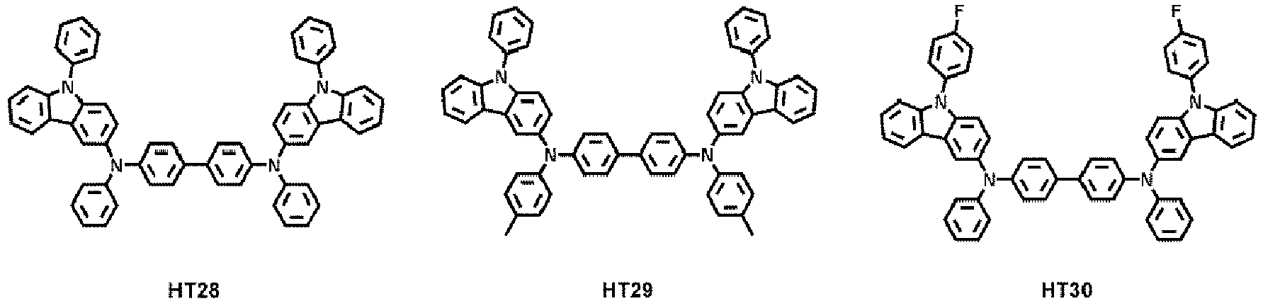


- A thickness of the hole transport region may be in a range of about 50 Å to about 10,000 Å, for example, about 100 Å to about 7,000 Å, about 100 Å to about 5,000 Å, about 100 Å to about 4,000 Å or about 100 Å to about 2,000 Å. When the hole transport region includes a hole injection layer, a hole transport layer, or any combination thereof, a thickness of the hole injection layer may be in a range of about 100 Å to about 9,000 Å, for example, about 100 Å to about 7,000 Å, about 100 Å to about 5,000 Å, about 100 Å to about 3,000 Å, about 100 Å to about 2,000 Å or about 100 Å to about 1,000 Å, and a thickness of the hole transport layer may be in a range of about 50 Å to about 2,000 Å, for example, about 100 Å to about 1,500 Å or about 300 Å to about 500 Å. When the thicknesses of the hole transport region, the hole injection layer, and the hole transport layer are within these ranges, satisfactory (or suitable) hole transporting characteristics may be obtained without a substantial increase in driving voltage.
- The emission auxiliary layer may increase light-emission efficiency by compensating for an optical resonance distance according to the wavelength of light emitted by the emission layers 130 and 140, and the electron blocking layer may block or reduce the flow of electrons from the electron transport region. The emission auxiliary layer and the electron blocking layer may include any of the materials described above.
- The hole transport region may further include, in addition to the materials described above, a charge-generation material for the improvement of conductive properties. The charge-generation material may be uniformly or non-uniformly dispersed in the hole transport region (for example, in the form of a single layer including or consisting of a charge-generation material).
- The charge-generation material may be, for example, a p-dopant.
- For example, a lowest unoccupied molecular orbital (LUMO) energy level of the p-dopant may be equal to or less than about -3.5 eV.
- In one or more embodiments, the p-dopant may include a quinone derivative, a cyano group-containing compound, a compound containing element EL1 and element EL2, or any combination thereof.
- Non-limiting examples of the quinone derivative are TCNQ, F4-TCNQ, and/or the like.
- Non-limiting examples of the cyano group-containing compound are HAT-CN, a compound represented by Formula 221, and/or the like:


- R221 to R223 may each independently be a C3-C60 (e.g. C3-C30) carbocyclic group unsubstituted or substituted with at least one R10a or a C1-C60 (e.g. C1-C20) heterocyclic group unsubstituted or substituted with at least one R10a,and
- at least one selected from R221 to R223 may each independently be a C3-C60 (e.g. C3-C30) carbocyclic group or a C1-C60 (e.g. C1-C20) heterocyclic group, each substituted with: a cyano group; -F; -CI; -Br; -I; a C1-C20 (e.g. C1-C10) alkyl group substituted with a cyano group, -F, -CI, -Br, -I, or any combination thereof; or any combination thereof.
- In the compound containing element EL1 and element EL2, element EL1 may be metal, metalloid, or a combination thereof, and element EL2 may be non-metal, metalloid, or a combination thereof.
- Examples of the metal are: alkali metal (for example, lithium (Li), sodium (Na), potassium (K), rubidium (Rb), cesium (Cs), etc.); alkaline earth metal (for example, beryllium (Be), magnesium (Mg), calcium (Ca), strontium (Sr), barium (Ba), etc.); transition metal (for example, titanium (Ti), zirconium (Zr), hafnium (Hf), vanadium (V), niobium (Nb), tantalum (Ta), chromium (Cr), molybdenum (Mo), tungsten (W), manganese (Mn), technetium (Tc), rhenium (Re), iron (Fe), ruthenium (Ru), osmium (Os), cobalt (Co), rhodium (Rh), iridium (Ir), nickel (Ni), palladium (Pd), platinum (Pt), copper (Cu), silver (Ag), gold (Au), etc.); post-transition metal (for example, zinc (Zn), indium (In), tin (Sn), etc.); and/or lanthanide metal (for example, lanthanum (La), cerium (Ce), praseodymium (Pr), neodymium (Nd), promethium (Pm), samarium (Sm), europium (Eu), gadolinium (Gd), terbium (Tb), dysprosium (Dy), holmium (Ho), erbium (Er), thulium (Tm), ytterbium (Yb), lutetium (Lu), etc.).
- Examples of the metalloid are silicon (Si), antimony (Sb), and/or tellurium (Te).
- Examples of the non-metal are oxygen (O) and/or halogen (for example, F, CI, Br, I, etc.).
- Examples of the compound containing element EL1 and element EL2 are metal oxide, metal halide (for example, metal fluoride, metal chloride, metal bromide, and/or metal iodide), metalloid halide (for example, metalloid fluoride, metalloid chloride, metalloid bromide, and/or metalloid iodide), metal telluride, or any combination thereof.
- Examples of the metal oxide are tungsten oxide (for example, WO, W2O3, WO2, WO3, W2O5, etc.), vanadium oxide (for example, VO, V2O3, VO2, V2O5, etc.), molybdenum oxide (MoO, Mo2O3, MoO2, MoO3 Mo2O5, etc.), and/or rhenium oxide (for example, ReO3, etc.).
- Examples of the metal halide are alkali metal halide, alkaline earth metal halide, transition metal halide, post-transition metal halide, and/or lanthanide metal halide.
- Examples of the alkali metal halide are LiF, NaF, KF, RbF, CsF, LiCI, NaCI, KCI, RbCI, CsCI, LiBr, NaBr, KBr, RbBr, CsBr, Lil, Nal, KI, Rbl, and/or Csl.
- Examples of the alkaline earth metal halide are BeF2, MgF2, CaF2, SrF2, BaF2, BeCl2, MgCl2, CaCl2, SrCl2, BaCl2, BeBr2, MgBr2, CaBr2, SrBr2, BaBr2, Bel2, Mgl2, Cal2, Srl2, and/or Bal2.
- Examples of the transition metal halide are titanium halide (for example, TiF4, TiCI4, TiBr4, Til4, etc.), zirconium halide (for example, ZrF4, ZrCl4, ZrBr4, Zrl4, etc.), hafnium halide (for example, HfF4, HfCl4, HfBr4, Hfl4, etc.), vanadium halide (for example, VF3, VCI3, VBr3, VI3, etc.), niobium halide (for example, NbF3, NbCl3, NbBr3, Nbl3, etc.), tantalum halide (for example, TaF3, TaCl3, TaBr3, Tal3, etc.), chromium halide (for example, CrF3, CrCl3, CrBr3, Crl3, etc.), molybdenum halide (for example, MoF3, MoCI3, MoBr3, Mol3, etc.), tungsten halide (for example, WF3, WCI3, WBr3, WI3, etc.), manganese halide (for example, MnF2, MnCl2, MnBr2, Mnl2, etc.), technetium halide (for example, TcF2, TcCl2, TcBr2, Tcl2, etc.), rhenium halide (for example, ReF2, ReCI2, ReBr2, Rel2, etc.), iron halide (for example, FeF2, FeCl2, FeBr2, Fel2, etc.), ruthenium halide (for example, RuF2, RuCl2, RuBr2, Rul2, etc.), osmium halide (for example, OsF2, OsCl2, OsBr2, Osl2, etc.), cobalt halide (for example, CoF2, CoCI2, CoBr2, Col2, etc.), rhodium halide (for example, RhF2, RhCl2, RhBr2, Rhl2, etc.), iridium halide (for example, IrF2, IrCl2, IrBr2, Irl2, etc.), nickel halide (for example, NiF2, NiCl2, NiBr2, Nil2, etc.), palladium halide (for example, PdF2, PdCl2, PdBr2, Pdl2, etc.), platinum halide (for example, PtF2, PtCl2, PtBr2, Ptl2, etc.), copper halide (for example, CuF, CuCI, CuBr, Cul, etc.), silver halide (for example, AgF, AgCI, AgBr, Agl, etc.), and/or gold halide (for example, AuF, AuCI, AuBr, Aul, etc.).
- Examples of the post-transition metal halide are zinc halide (for example, ZnF2, ZnCl2, ZnBr2, Znl2, etc.), indium halide (for example, lnl3, etc.), and/or tin halide (for example, Snl2, etc.).
- Examples of the lanthanide metal halide are YbF, YbF2, YbF3, SmF3, YbCI, YbCl2, YbCl3, SmCl3, YbBr, YbBr2, YbBr3 SmBr3, Ybl, Ybl2, Ybl3, and/or Sml3.
- An example of the metalloid halide is antimony halide (for example, SbCl5, etc.).
- Examples of the metal telluride are alkali metal telluride (for example, Li2Te, Na2Te, K2Te, Rb2Te, Cs2Te, etc.), alkaline earth metal telluride (for example, BeTe, MgTe, CaTe, SrTe, BaTe, etc.), transition metal telluride (for example, TiTe2, ZrTe2, HfTe2, V2Te3, Nb2Te3, Ta2Te3, Cr2Te3, Mo2Te3, W2Te3, MnTe, TcTe, ReTe, FeTe, RuTe, OsTe, CoTe, RhTe, IrTe, NiTe, PdTe, PtTe, Cu2Te, CuTe, Ag2Te, AgTe, Au2Te, etc.), post-transition metal telluride (for example, ZnTe, etc.), and/or lanthanide metal telluride (for example, LaTe, CeTe, PrTe, NdTe, PmTe, EuTe, GdTe, TbTe, DyTe, HoTe, ErTe, TmTe, YbTe, LuTe, etc.).
- The
emission layer 150 may include thefirst emission layer 130 and thesecond emission layer 140. Thefirst emission layer 130 and thesecond emission layer 140 may each be the same as described herein. - The
first emission layer 130 may include firstquantum dots 131, and thesecond emission layer 140 may include secondquantum dots 141. The firstquantum dots 131 and the secondquantum dots 141 may each be the same as described herein. - The
first emission layer 130 may be in direct contact with thesecond emission layer 140. - In one or more embodiments, the host may include a compound represented by Formula 301:
Formula 301 [Ar301]xb11-[(L301)xb1-R301]xb21 ,
wherein, in Formula 301, - Ar301 and L301 may each independently be a C3-C60 (e.g. C3-C30) carbocyclic group unsubstituted or substituted with at least one R10a or a C1-C60 (e.g. C1-C20) heterocyclic group unsubstituted or substituted with at least one R10a,
- xb11 may be 1, 2, or 3,
- xb1 may be an integer from 0 to 5,
- R301 may be hydrogen, deuterium, -F, -CI, -Br, -I, a hydroxyl group, a cyano group, a nitro group, a C1-C60 (e.g. C1-C20) alkyl group unsubstituted or substituted with at least one R10a, a C2-C60 (e.g. C2-C20) alkenyl group unsubstituted or substituted with at least one R10a,a C2-C60 (e.g. C2-C20) alkynyl group unsubstituted or substituted with at least one R10a,a C1-C60 (e.g. C1-C20) alkoxy group unsubstituted or substituted with at least one R10a,a C3-C60 (e.g. C3-C30) carbocyclic group unsubstituted or substituted with at least one R10a, a C1-C60 (e.g. C1-C20) heterocyclic group unsubstituted or substituted with at least one R10a, -Si(Q301)(Q302)(Q303), -N(Q301)(Q302), -B(Q301)(Q302), - C(=O)(Q301), -S(=O)2(Q301), or -P(=O)(Q301)(Q302),
- xb21 may be an integer from 1 to 5, and
- Q301 to Q303 may each be the same as described in connection with Q11.
- For example, when xb11 in Formula 301 is 2 or more, two or more of Ar301(s) may be linked to each other via a single bond.
- In one or more embodiments, the host may include a compound represented by Formula 301-1, a compound represented by Formula 301-2, or any combination thereof:


- ring A301 to ring A304 may each independently be a C3-C60 (e.g. C3-C30) carbocyclic group unsubstituted or substituted with at least one R10a or a C1-C60 (e.g. C1-C20) heterocyclic group unsubstituted or substituted with at least one R10a,
- X301 may be O, S, N-[(L304)xb4-R304], C(R304)(R305), or Si(R304)(R305),
- xb22 and xb23 may each independently be 0, 1, or 2,
- L301, xb1, and R301 may each be the same as described herein,
- L302 to L304 may each independently be the same as described in connection with L301,
- xb2 to xb4 may each independently be the same as described in connection with xb1, and
- R302 to R305 and R311 to R314 may each be the same as described in connection with R301.
- In one or more embodiments, the host may include an alkaline earth-metal complex. In one or more embodiments, the host may include a Be complex (for example, Compound H55), an Mg complex, a Zn complex, or any combination thereof.
- In one or more embodiments, the host may include any of Compounds H1 to H124, 9,10-di(2-naphthyl)anthracene (ADN), 2-methyl-9,10-bis(naphthalen-2-yl)anthracene (MADN), 9,10-di-(2-naphthyl)-2-t-butyl-anthracene (TBADN), 4,4'-bis(N-carbazolyl)-1,1'-biphenyl (CBP), 1,3-di-9-carbazolylbenzene (mCP), 1,3,5-tri(carbazol-9-yl)benzene (TCP), or any combination thereof:


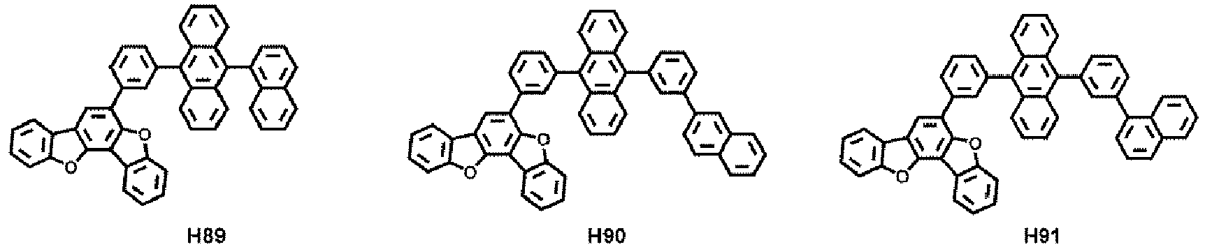





- The phosphorescent dopant may include at least one transition metal as a central metal.
- The phosphorescent dopant may include a monodentate ligand, a bidentate ligand, a tridentate ligand, a tetradentate ligand, a pentadentate ligand, a hexadentate ligand, or any combination thereof.
- The phosphorescent dopant may be electrically neutral.
- For example, the phosphorescent dopant may include an organometallic compound represented by Formula 401:
Formula 401 M (L401 )xc1(L402)xc2

- M may be transition metal (for example, iridium (Ir), platinum (Pt), palladium (Pd), osmium (Os), titanium (Ti), gold (Au), hafnium (Hf), europium (Eu), terbium (Tb), rhodium (Rh), rhenium (Re), or thulium (Tm)),
- L401 may be a ligand represented by Formula 402, and xc1 may be 1, 2, or 3, wherein, when xc1 is 2 or more, two or more of L401(S) may be identical to or different from each other,
- L402 may be an organic ligand, and xc2 may be 0, 1, 2, 3, or 4, wherein, when xc2 is 2 or more, two or more of L402(S) may be identical to or different from each other,
- X401 and X402 may each independently be nitrogen or carbon,
- ring A401 and ring A402 may each independently be a C3-C60 (e.g. C3-C30) carbocyclic group or a C1-C60 (e.g. C1-C20) heterocyclic group,
- T401 may be a single bond, *-0-*', *-S-*', *-C(=O)-*', *-N(Q411)-*', *-C(Q411)(Q412)-*', *-C(Q411)=C(Q412)-*', *-C(Q411)=*', or *=C=*',
- X403 and X404 may each independently be a chemical bond (for example, a covalent bond or a coordinate bond), O, S, N(Q413), B(Q413), P(Q413), C(Q413)(Q414), or Si(Q413)(Q414),
- Q411 to Q414 may each be the same as described in connection with Q11,
- R401 and R402 may each independently be hydrogen, deuterium, -F, -CI, -Br, - I, a hydroxyl group, a cyano group, a nitro group, a C1-C20 alkyl group unsubstituted or substituted with at least one R10a,a C1-C20 alkoxy group unsubstituted or substituted with at least one R10a,a C3-C60 (e.g. C3-C30) carbocyclic group unsubstituted or substituted with at least one R10a, a C1-C60 (e.g. C1-C20) heterocyclic group unsubstituted or substituted with at least one R10a,-Si(Q401)(Q402)(Q403), -N(Q401)(Q402), -B(Q401)(Q402), -C(=O)(Q401), -S(=O)2(Q401), or -P(=O)(Q401)(Q402),
- Q401 to Q403 may each be the same as described in connection with Q11,
- xc11 and xc12 may each independently be an integer from 0 to 10, and
- * and *' in Formula 402 each indicate a binding site to M in Formula 401.
- For example, in Formula 402, i) X401 may be nitrogen and X402 may be carbon, or ii) each of X401 and X402 may be nitrogen.
- In one or more embodiments, in Formula 401, when xc1 is 2 or more, two rings A401(s) in two or more of L401(s) may be optionally linked to each other via T402, which is a linking group, and two rings A402(s) may optionally be linked to each other via T403, which is a linking group (see e.g., Compounds PD1 to PD4 and PD7), wherein T402 and T403 may each be the same as described in connection with T401.
- In Formula 401, L402 may be an organic ligand. For example, L402 may include a halogen group, a diketone group (for example, an acetylacetonate group), a carboxylic acid group (for example, a picolinate group), -C(=O), an isonitrile group, -CN group, a phosphorus group (for example, a phosphine group, a phosphite group, etc.), or any combination thereof.
- The phosphorescent dopant may include, for example, one of compounds PD1 to PD25, or any combination thereof:


- The fluorescent dopant may include an amine group-containing compound, a styryl group-containing compound, or any combination thereof.
- In one or more embodiments, the fluorescent dopant may include a compound represented by Formula 501:

- Ar501, L501 to L503, R501, and R502 may each independently be a C3-C60 (e.g. C3-C30) carbocyclic group unsubstituted or substituted with at least one R10a or a C1-C60 (e.g. C1-C20) heterocyclic group unsubstituted or substituted with at least one R10a,
- xd1 to xd3 may each independently be 0, 1, 2, or 3, and
- xd4 may be 1, 2, 3, 4, 5, or 6.
- In one or more embodiments, Ar501 in Formula 501 may be a condensed cyclic group (for example, an anthracene group, a chrysene group, or a pyrene group) in which three or more monocyclic groups are condensed together.
- In one or more embodiments, xd4 in Formula 501 may be 2.
- For example, the fluorescent dopant may include any of Compounds FD1 to FD36, DPVBi, DPAVBi, or any combination thereof:


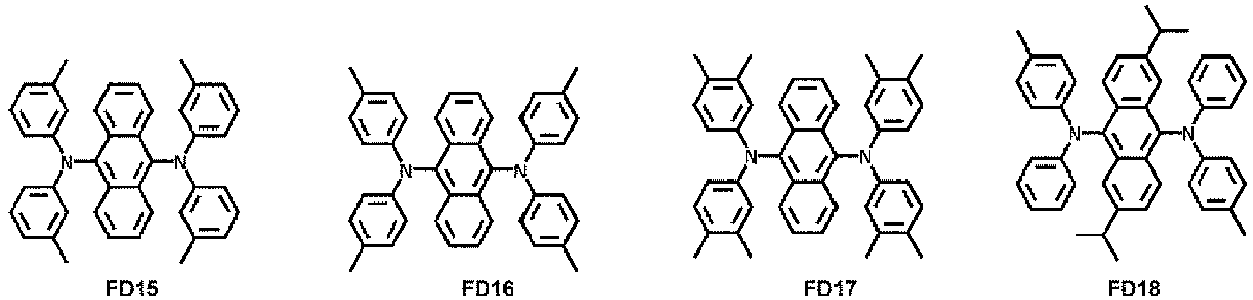


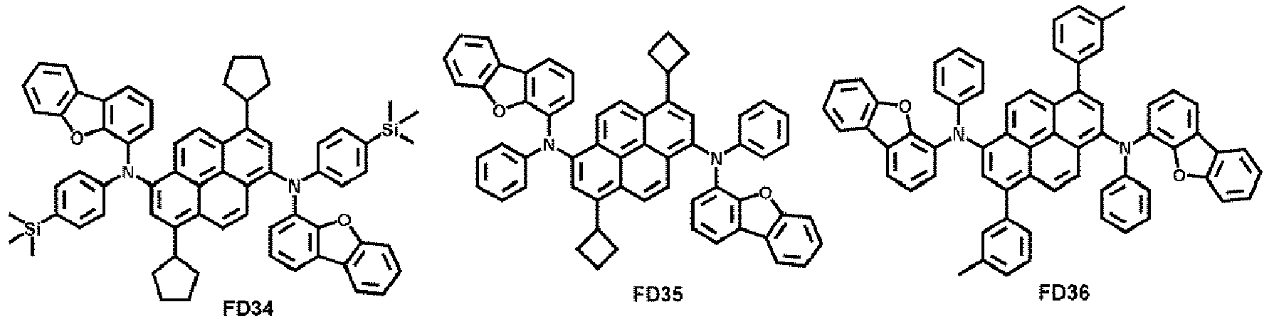

- The emission layer may include a delayed fluorescence material.
- In the present specification, the delayed fluorescence material may be selected from compounds capable of emitting delayed fluorescence based on a delayed fluorescence emission mechanism.
- The delayed fluorescent material included in the emission layer may act as a host or a dopant depending on the type (or kind) of other materials included in the emission layer.
- In one or more embodiments, a difference between a triplet energy level (eV) of the delayed fluorescence material and a singlet energy level (eV) of the delayed fluorescence material may be equal to or greater than 0 eV and equal to or less than about 0.5 eV. When the difference between the triplet energy level (eV) of the delayed fluorescence material and the singlet energy level (eV) of the delayed fluorescence material is satisfied within the range above, up-conversion from the triplet state to the singlet state of the delayed fluorescence materials may effectively (or suitably) occur, and thus, the light-emitting
device 10 may have improved luminescence efficiency. - In one or more embodiments, the delayed fluorescence material may include i) a material including at least one electron donor (for example, a π electron-rich C3-C60 (e.g. C3-C30) cyclic group, such as a carbazole group) and at least one electron acceptor (for example, a sulfoxide group, a cyano group, and/or a π electron-deficient nitrogen-containing C1-C60 (e.g. C1-C30) cyclic group), and ii) a material including a C8-C60 (e.g. C8-C30) polycyclic group in which two or more cyclic groups are condensed while sharing boron (B).
- In one or more embodiments, the delayed fluorescence material may include at least one of Compounds DF1 to DF9:


- The electron transport region may have: i) a single-layered structure including or consisting of a single layer including or consisting of a single material, ii) a single-layered structure including or consisting of a single layer including or consisting of a plurality of different materials, or iii) a multi-layered structure including a plurality of layers including different materials.
- The electron transport region may include a buffer layer, a hole blocking layer, an electron control layer, an electron transport layer, an electron injection layer, or any combination thereof.
- For example, the electron transport region may have an electron transport layer/electron injection layer structure, a hole blocking layer/electron transport layer/electron injection layer structure, an electron control layer/electron transport layer/electron injection layer structure, or a buffer layer/electron transport layer/electron injection layer structure, wherein, in each structure, layers are sequentially stacked on the emission layers 130 and 140.
- The electron transport region (for example, the buffer layer, the hole blocking layer, the electron control layer, and/or the electron transport layer in the electron transport region) may include a metal-free compound including at least one π electron-deficient nitrogen-containing C1-C60 (e.g. C1-C30) cyclic group.
- In one or more embodiments, the electron transport region may include a compound represented by Formula 601:
Formula 601 [Ar601]xe11-[(L601)xe1-R601]xe21,
wherein, in Formula 601, - Ar601 and L601 may each independently be a C3-C60 (e.g. C3-C30) carbocyclic group unsubstituted or substituted with at least one R10a or a C1-C60 (e.g. C1-C20) heterocyclic group unsubstituted or substituted with at least one R10a,
- xe11 may be 1, 2, or 3,
- xe1 may be 0, 1, 2, 3, 4, or 5,
- R601 may be a C3-C60 (e.g. C3-C30) carbocyclic group unsubstituted or substituted with at least one R10a, a C1-C60 (e.g. C1-C20) heterocyclic group unsubstituted or substituted with at least one R10a,-Si(Q601)(Q602)(Q603), -C(=O)(Q601), - S(=O)2(Q601), or -P(=O)(Q601)(Q602),
- Q601 to Q603 may each be the same as described in connection with Q11,
- xe21 may be 1, 2, 3, 4, or 5, and
- at least one of Ar601, L601, or R601 may each independently be a π electron-deficient nitrogen-containing C1-C60 (e.g. C1-C30) cyclic group unsubstituted or substituted with at least one Rioa.
- In one or more embodiments, when xe11 in Formula 601 is 2 or more, two or more of Ar601(s) may be linked together via a single bond.
- In one or more embodiments, Ar601 in Formula 601 may be a substituted or unsubstituted anthracene group.
- In one or more embodiments, the electron transport region may include a compound represented by Formula 601-1:

- X614 may be N or C(R614), X615 may be N or C(R615), and X616 may be N or C(R616), wherein at least one of X614 to X616 may be N,
- L611 to L613 may each be the same as described in connection with L601,
- xe611 to xe613 may each be the same as described in connection with xe1,
- R611 to R613 may each be the same as described in connection with R601, and
- R614 to R616 may each independently be hydrogen, deuterium, -F, -CI, -Br, -I, a hydroxyl group, a cyano group, a nitro group, a C1-C20 (e.g. C1-C10) alkyl group, a C1-C20 (e.g. C1-C10) alkoxy group, a C3-C60 (e.g. C3-C30) carbocyclic group unsubstituted or substituted with at least one R10a, or a C1-C60 (e.g. C1-C20) heterocyclic group substituted or unsubstituted at least one Rioa.
- For example, xe1 and xe611 to xe613 in Formulae 601 and 601-1 may each independently be 0, 1, or 2.
- The electron transport region may include any of Compounds ET1 to ET45, 2,9-dimethyl-4,7-diphenyl-1,10-phenanthroline (BCP), 4,7-diphenyl-1,10-phenanthroline (Bphen), Alq3, BAIq, TAZ, NTAZ, or any combination thereof:


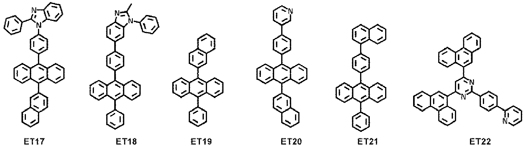


- A thickness of the electron transport region may be in a range about 50 Å to about 5,000 Å, for example, about 100 Å to about 4,000 Å or about 100 Å to about 1,000 Å. When the electron transport region includes a buffer layer, a hole blocking layer, an electron control layer, an electron transport layer, or any combination thereof, a thickness of the buffer layer, the hole blocking layer, or the electron control layer may each independently be in a range of about 20 Å to about 1000 Å, for example, about 20 Å to about 700 Å, about 20 Å to about 500 Å, about 20 Å to about 400 Å, about 30 Å to about 400 Å or about 30 Å to about 300 Å, and a thickness of the electron transport layer may be in a range of about 100 Å to about 1000 Å, for example, about 100 Å to about 700 Å, about 100 Å to about 600 Å, about 150 Å to about 600 Å, about 150 Å to about 500 Å or about 600 Å to about 800 Å. When the thicknesses of the buffer layer, the hole blocking layer, the electron control layer, the electron transport layer, and/or the electron transport layer are within these ranges, satisfactory (or suitable) electron transporting characteristics may be obtained without a substantial increase in driving voltage.
- The electron transport region (for example, the electron transport layer in the electron transport region) may further include, in addition to the materials described above, a metal-containing material.
- The metal-containing material may include an alkali metal complex, alkaline earth metal complex, or any combination thereof. A metal ion of the alkali metal complex may be a Li ion, a Na ion, a K ion, a Rb ion, or a Cs ion; and a metal ion of the alkaline earth metal complex may be a Be ion, a Mg ion, a Ca ion, a Sr ion, or a Ba ion. A ligand coordinated with the metal ion of the alkali metal complex or the alkaline earth-metal complex may include a hydroxyquinoline, a hydroxyisoquinoline, a hydroxybenzoquinoline, a hydroxyacridine, a hydroxyphenanthridine, a hydroxyphenyloxazole, a hydroxyphenylthiazole, a hydroxyphenyloxadiazole, a hydroxyphenylthiadiazole, a hydroxyphenylpyridine, a hydroxyphenylbenzimidazole, a hydroxyphenylbenzothiazole, a bipyridine, a phenanthroline, a cyclopentadiene, or any combination thereof.
- For example, the metal-containing material may include a Li complex. The Li complex may include, for example, Compound ET-D1 (LiQ) and/or Compound ET-D2:

- The electron transport region may include an electron injection layer that facilitates the injection of electrons from the
second electrode 190. The electron injection layer may be in direct contact with thesecond electrode 190. - The electron injection layer may have: i) a single-layered structure including or consisting of a single layer including or consisting of a single material, ii) a single-layered structure including or consisting of a single layer including or consisting of a plurality of different materials, or iii) a multi-layered structure including a plurality of layers including different materials.
- The electron injection layer may include an alkali metal, alkaline earth metal, a rare earth metal, an alkali metal-containing compound, alkaline earth metal-containing compound, a rare earth metal-containing compound, an alkali metal complex, alkaline earth metal complex, a rare earth metal complex, or any combination thereof.
- The alkali metal may include Li, Na, K, Rb, Cs, or any combination thereof. The alkaline earth metal may include Mg, Ca, Sr, Ba, or any combination thereof. The rare earth metal may include Sc, Y, Ce, Tb, Yb, Gd, or any combination thereof.
- The alkali metal-containing compound, the alkaline earth metal-containing compound, and the rare earth metal-containing compound may be one or more oxides, halides (for example, fluorides, chlorides, bromides, and/or iodides), tellurides, or any combination thereof, of the alkali metal, the alkaline earth metal, and the rare earth metal, respectively.
- The alkali metal-containing compound may include one or more alkali metal oxides (such as Li2O, Cs2O, and/or K2O), alkali metal halides (such as LiF, NaF, CsF, KF, Lil, Nal, Csl, and/or Kl), or any combination thereof. The alkaline earth metal-containing compound may include an alkaline earth metal compound, such as BaO, SrO, CaO, BaxSr1-xO (where x is a real number satisfying the condition of 0<x<1), BaxCa1-xO (where x is a real number satisfying the condition of 0<x<1), and/or the like. The rare earth metal-containing compound may include YbF3, ScF3, Sc2O3, Y2O3, Ce2O3, GdF3, TbF3, Ybl3, Scl3, Tbl3, or any combination thereof. For example, the rare earth metal-containing compound may include lanthanide metal telluride. Non-limiting examples of the lanthanide metal telluride are LaTe, CeTe, PrTe, NdTe, PmTe, SmTe, EuTe, GdTe, TbTe, DyTe, HoTe, ErTe, TmTe, YbTe, LuTe, La2Te3, Ce2Te3, Pr2Te3, Nd2Te3, Pm2Te3, Sm2Te3, Eu2Te3, Gd2Te3, Tb2Te3, Dy2Te3, Ho2Te3, Er2Te3, Tm2Te3, Yb2Te3, and/or Lu2Te3.
- The alkali metal complex, the alkaline earth-metal complex, and the rare earth metal complex may include i) one of ions of the alkali metal, the alkaline earth metal, or the rare earth metal and ii), as a ligand bonded to the metal ion, for example, a hydroxyquinoline, a hydroxyisoquinoline, a hydroxybenzoquinoline, a hydroxyacridine, a hydroxyphenanthridine, a hydroxyphenyloxazole, a hydroxyphenylthiazole, a hydroxyphenyloxadiazole, a hydroxyphenylthiadiazole, a hydroxyphenylpyridine, a hydroxyphenyl benzimidazole, a hydroxyphenylbenzothiazole, a bipyridine, a phenanthroline, a cyclopentadiene, or any combination thereof.
- The electron injection layer may include or consist of an alkali metal, an alkaline earth metal, a rare earth metal, an alkali metal-containing compound, an alkaline earth metal-containing compound, a rare earth metal-containing compound, an alkali metal complex, an alkaline earth metal complex, a rare earth metal complex, or any combination thereof, as described above. For example, the electron injection layer may further include an organic material (for example, a compound represented by Formula 601).
- In one or more embodiments, the electron injection layer may include or consist of i) an alkali metal-containing compound (for example, an alkali metal halide), or ii) a) an alkali metal-containing compound (for example, an alkali metal halide); and b) an alkali metal, an alkaline earth metal, a rare earth metal, or any combination thereof. For example, the electron injection layer may be a KI:Yb co-deposited layer, an Rbl:Yb co-deposited layer, and/or the like.
- When the electron injection layer further includes an organic material, the alkali metal, the alkaline earth metal, the rare earth metal, the alkali metal-containing compound, the alkaline earth metal-containing compound, the rare earth metal-containing compound, the alkali metal complex, the alkaline earth-metal complex, the rare earth metal complex, or any combination thereof may be homogeneously or non-homogeneously dispersed in a matrix including the organic material.
- A thickness of the electron injection layer may be in a range of about 1 Å to about 100 Å, for example, about 3 Å to about 90 Å or about 3 Å to about 20 Å. When the thickness of the electron injection layer is within these ranges, satisfactory (or suitable) electron injection characteristics may be obtained without a substantial increase in driving voltage.
- The
second electrode 190 is arranged on theinterlayer 150 having the above-described structure. Thesecond electrode 190 may be a cathode, which is an electron injection electrode, and in this regard, as a material for forming thesecond electrode 190, a metal, an alloy, a suitable electrically conductive compound, or any combination thereof, each having a low work function, may be used. - The
second electrode 190 may include at least one of lithium (Li), silver (Ag), magnesium (Mg), aluminium (Al), aluminium-lithium (Al-Li), calcium (Ca), magnesium-indium (Mg-In), magnesium-silver (Mg-Ag), ytterbium (Yb), silver-ytterbium (Ag-Yb), ITO, IZO, or any combination thereof. Thesecond electrode 190 may be a transmissive electrode, a semi-transmissive electrode, or a reflective electrode. - The
second electrode 190 may have a single-layered structure or a multi-layered structure including two or more layers. - A first capping layer may be arranged outside the
first electrode 110, and/or a second capping layer may be arranged outside thesecond electrode 190. For example, the light-emitting device 100 may have a structure in which the first capping layer, thefirst electrode 110, theinterlayer 150, and thesecond electrode 190 are sequentially stacked in this stated order; a structure in which thefirst electrode 110, theinterlayer 150, thesecond electrode 190, and the second capping layer are sequentially stacked in this stated order; or a structure in which the first capping layer, thefirst electrode 110, theinterlayer 150 , thesecond electrode 190, and the second capping layer are sequentially stacked in this stated order. - Light generated in the
emission layer interlayer 150 of the light-emittingdevice 10 may be extracted toward the outside through thefirst electrode 110, which is a semi-transmissive electrode or a transmissive electrode, and the first capping layer, and/or light generated in theemission layer interlayer 150 of the light-emittingdevice 10 may be extracted toward the outside through thesecond electrode 150, which is a semi-transmissive electrode or a transmissive electrode, and the second capping layer. - The first capping layer and the second capping layer may increase external luminescence efficiency according to the principle of constructive interference. Accordingly, light extraction efficiency of the light-emitting
device 10 may be increased, thereby improving luminescence efficiency of the light-emittingdevice 10. - Each of the first capping layer and second capping layer may include a material having a refractive index (at 589 nm) of equal to or more than about 1.6.
- The first capping layer and the second capping layer may each independently be an organic capping layer including an organic material, an inorganic capping layer including an inorganic material, or a composite capping layer including an organic material and an inorganic material.
- At least one of the first capping layer or the second capping layer may each independently include a carbocyclic compound, a heterocyclic compound, an amine group-containing compound, a porphyrin derivative, a phthalocyanine derivative, a naphthalocyanine derivative, an alkali metal complex, an alkaline earth-based complex, or any combination thereof. The carbocyclic compound, the heterocyclic compound, and the amine group-containing compound may each independently be optionally be substituted with a substituent containing O, N, S, Se, Si, F, Cl, Br, I, or any combination thereof. In one or more embodiments, at least one of the first capping layer or the second capping layer may each independently include the amine group-containing compound.
- In one or more embodiments, at least one of the first capping layer or the second capping layer may each independently include a compound represented by Formula 201, a compound represented by Formula 202, or any combination thereof.
- In one or more embodiments, at least one of the first capping layer or the second capping layer may each independently include any of Compounds HT28 to HT33, any of Compounds CP1 to CP6, β-NPB, or any combination thereof:


- The light-emitting device may be included in various suitable electronic apparatuses. For example, an electronic apparatus including the light-emitting device may be a light-emitting apparatus, an authentication apparatus, and/or the like.
- Such an electronic apparatus (for example, light-emitting apparatus) may further include, in addition to the light-emitting device, i) a color filter, ii) a color conversion layer, or iii) both a color filter and a color conversion layer. The color filter and/or the color conversion layer may be arranged in at least one traveling direction of light emitted from the light-emitting device. For example, light emitted from the light-emitting device may be blue light or white light. The light-emitting device may be the same as described above. In one or more embodiments, the color conversion layer may include quantum dots. The quantum dots may be, for example, the same as described herein.
- The electronic apparatus may include a first substrate. The first substrate may include a plurality of subpixel areas, the color filter may include a plurality of color filter areas respectively corresponding to the subpixel areas, and the color conversion layer may include a plurality of color conversion areas respectively corresponding to the subpixel areas.
- A pixel-defining film may be arranged among the subpixel areas to define each of the subpixel areas.
- The color filter may further include a plurality of color filter areas, and light-blocking patterns located among the color filter areas, and the color conversion layer may include a plurality of color conversion areas, and light-blocking patterns located among the color conversion areas.
- The color filter areas (and/or the color conversion areas) may include a first area to emit first color light, a second area to emit second color light, and/or a third area to emit third color light, and the first color light, the second color light, and/or the third color light may have different maximum emission wavelengths from one another. For example, the first color light may be red light, the second color light may be green light, and the third color light may be blue light. For example, the color filter areas (and/or the color conversion areas) may include quantum dots. In one or more embodiments, the first area may include red quantum dots, the second area may include green quantum dots, and the third area may not include quantum dots. The quantum dots may be the same as described herein. The first area, the second area, and/or the third area may each include a scatter.
- For example, the light-emitting device may emit first light, the first area may absorb the first light to emit first first-color light, the second area may absorb the first light to emit second first-color light, and the third area may absorb the first light to emit third first-color light. Here, the first first-color light, the second first-color light, and the third-first light may have different maximum emission wavelengths from one another. For example, the first light may be blue light, the first first-color light may be red light, the second first-color light may be green light, and the third first-color light may be blue light.
- The electronic apparatus may further include a thin-film transistor, in addition to the light-emitting device as described above. The thin-film transistor may include a source electrode, a drain electrode, and an active layer, wherein any one of the source electrode and the drain electrode may be electrically connected to any one of the first electrode and the second electrode of the light-emitting device.
- The thin-film transistor may include a gate electrode, a gate insulating film, and/or the like.
- The active layer may include crystalline silicon, amorphous silicon, organic semiconductor, oxide semiconductor, and/or the like.
- The electronic apparatus may further include a sealing portion for sealing the light-emitting device. The sealing portion may be arranged between the color filter and the light-emitting device and/or between the color conversion layer and the light-emitting device. The sealing portion allows light from the light-emitting device to be extracted to the outside, while simultaneously (or concurrently) preventing or reducing the penetration of ambient air and/or moisture into the light-emitting device. The sealing portion may be a sealing substrate including a transparent glass substrate and/or a plastic substrate. The sealing portion may be a thin-film encapsulation layer including at least one layer of an organic layer and/or an inorganic layer. When the sealing portion is a thin-film encapsulation layer, the electronic apparatus may be flexible.
- Various suitable functional layers may be additionally arranged on the sealing portion, in addition to the color filter and/or the color conversion layer, according to the use of the electronic apparatus. The functional layers may include a touch screen layer, a polarizing layer, and/or the like. The touch screen layer may be a pressure-sensitive touch screen layer, a capacitive touch screen layer, or an infra-red touch screen layer. The authentication apparatus may be, for example, a biometric authentication apparatus that authenticates an individual by using biometric information of a living body (for example, fingertips, pupils, etc.).
- The authentication apparatus may further include, in addition to the light-emitting device, a biometric information collector.
- The electronic apparatus may be applied to various suitable displays, light sources, lighting, personal computers (for example, a mobile personal computer), mobile phones, digital cameras, electronic organizers, electronic dictionaries, electronic game machines, medical instruments (for example, electronic thermometers, sphygmomanometers, blood glucose meters, pulse measurement devices, pulse wave measurement devices, electrocardiogram displays, ultrasonic diagnostic devices, and/or endoscope displays), fish finders, various measuring instruments, meters (for example, meters for a vehicle, an aircraft, and/or a vessel), projectors, and/or the like.
- Respective layers included in the hole transport region, the emission layer, and respective layers included in the electron transport region may be formed in a certain region by using one or more suitable methods including vacuum deposition, spin coating, casting, Langmuir-Blodgett (LB) deposition, ink-jet printing, laser-printing, laser-induced thermal imaging, and/or the like.
- When respective layers included in the hole transport region, the emission layer, and respective layers included in the electron transport region are formed by vacuum deposition, the deposition conditions may include, for example, a deposition temperature in a range of about 100 °C to about 500 °C, a vacuum degree of about 10-8 torr to about 10-3 torr, and a deposition speed in a range of about 0.01 Å/sec to about 100 Å/sec, depending on a material to be included in a layer to be formed and a structure of a layer to be formed.
- The term "C3-C60 carbocyclic group" as used herein refers to a cyclic group consisting of carbon atoms only and having three to sixty carbon atoms, and the term "C1-C60 heterocyclic group" as used herein refers to a cyclic group that further includes a heteroatom in addition to 1 to 60 carbon atoms. The C3-C60 carbocyclic group and the C1-C60 heterocyclic group may each independently be a monocyclic group consisting of one ring, or a polycyclic group in which two or more rings are condensed with each other. For example, the number of ring-forming atoms of the C1-C60 heterocyclic group may be from 3 to 61.
- The "cyclic group" as used herein may include both the C3-C60 carbocyclic group and the C1-C60 heterocyclic group.
- The term "π electron-rich C3-C60 cyclic group" as used herein refers to a cyclic group that includes 3 to 60 carbon atoms and does not include *-N=*' as a ring-forming moiety, and the term "π electron-deficient nitrogen-containing C1-C60 cyclic group" as used herein refers to a heterocyclic group that includes 1 to 60 carbon atoms and includes *-N=*' as a ring-forming moiety.
- For example,
- the C3-C60 carbocyclic group may be i) group T1 or ii) a condensed cyclic group in which two or more groups T1 are condensed with each other (for example, the C3-C60 carbocyclic group may be a cyclopentadiene group, an adamantane group, a norbornane group, a benzene group, a pentalene group, a naphthalene group, an azulene group, an indacene group, an acenaphthylene group, a phenalene group, a phenanthrene group, an anthracene group, a fluoranthene group, a triphenylene group, a pyrene group, a chrysene group, a perylene group, a pentaphene group, a heptalene group, a naphthacene group, a picene group, a hexacene group, a pentacene group, a rubicene group, a coronene group, an ovalene group, an indene group, a fluorene group, a spiro-bifluorene group, a benzofluorene group, an indenophenanthrene group, and/or an indenoanthracene group),
- the C1-C60 heterocyclic group may be i) group T2, ii) a condensed cyclic group in which two or more groups T2 are condensed with each other, or iii) a condensed cyclic group in which at least one group T2 and at least one group T1 are condensed with each other (for example, the C1-C60 heterocyclic group may be a pyrrole group, a thiophene group, a furan group, an indole group, a benzoindole group, a naphtho indole group, an isoindole group, a benzoisoindole group, a naphtho isoindole group, a benzosilole group, a benzothiophene group, a benzofuran group, a carbazole group, a dibenzosilole group, a dibenzothiophene group, a dibenzofuran group, an indenocarbazole group, an indolocarbazole group, a benzofurocarbazole group, a benzothienocarbazole group, a benzosilolocarbazole group, a benzoindolocarbazole group, a benzocarbazole group, a benzonaphthofuran group, a benzonaphthothiophene group, a benzonaphthosilole group, a benzofurodibenzofuran group, a benzofurodibenzothiophene group, a benzothienodibenzothiophene group, a pyrazole group, an imidazole group, a triazole group, an oxazole group, an isoxazole group, an oxadiazole group, a thiazole group, an isothiazole group, a thiadiazole group, a benzopyrazole group, a benzimidazole group, a benzoxazole group, a benzoisoxazole group, a benzothiazole group, a benzoisothiazole group, a pyridine group, a pyrimidine group, a pyrazine group, a pyridazine group, a triazine group, a quinoline group, an isoquinoline group, a benzoquinoline group, a benzoisoquinoline group, a quinoxaline group, a benzoquinoxaline group, a quinazoline group, a benzoquinazoline group, a phenanthroline group, a cinnoline group, a phthalazine group, a naphthyridine group, an imidazopyridine group, an imidazopyrimidine group, an imidazotriazine group, an imidazopyrazine group, an imidazopyridazine group, an azacarbazole group, an azafluorene group, an azadibenzosilole group, an azadibenzothiophene group, an azadibenzofuran group, etc.),
- the π electron-rich C3-C60 cyclic group may be i) group T1, ii) a condensed cyclic group in which two or more groups T1 are condensed with each other, iii) group T3, iv) a condensed cyclic group in which two or more groups T3 are condensed with each other, or v) a condensed cyclic group in which at least one group T3 and at least one group T1 are condensed with each other (for example, the π electron-rich C3-C60 cyclic group may be the C3-C60 carbocyclic group, a pyrrole group, a thiophene group, a furan group, an indole group, a benzoindole group, a naphtho indole group, an isoindole group, a benzoisoindole group, a naphtho isoindole group, a benzosilole group, a benzothiophene group, a benzofuran group, a carbazole group, a dibenzosilole group, a dibenzothiophene group, a dibenzofuran group, an indenocarbazole group, an indolocarbazole group, a benzofurocarbazole group, a benzothienocarbazole group, a benzosilolocarbazole group, a benzoindolocarbazole group, a benzocarbazole group, a benzonaphthofuran group, a benzonaphthothiophene group, a benzonaphthosilole group, a benzofurodibenzofuran group, a benzofurodibenzothiophene group, a benzothienodibenzothiophene group, etc.),
- the π electron-deficient nitrogen-containing C1-C60 cyclic group may be i) group T4, ii) a condensed cyclic group in which two or more groups T4 are condensed with each other, iii) a condensed cyclic group in which at least one group T4 and at least one group T1 are condensed with each other, iv) a condensed cyclic group in which at least one group T4 and at least one group T3 are condensed with each other, or v) a condensed cyclic group in which at least one group T4, at least one group T1, and at least one group T3 are condensed with one another (for example, the π electron-deficient nitrogen-containing C1-C60 cyclic group may be a pyrazole group, an imidazole group, a triazole group, an oxazole group, an isoxazole group, an oxadiazole group, a thiazole group, an isothiazole group, a thiadiazole group, a benzopyrazole group, a benzimidazole group, a benzoxazole group, a benzoisoxazole group, a benzothiazole group, a benzoisothiazole group, a pyridine group, a pyrimidine group, a pyrazine group, a pyridazine group, a triazine group, a quinoline group, an isoquinoline group, a benzoquinoline group, a benzoisoquinoline group, a quinoxaline group, a benzoquinoxaline group, a quinazoline group, a benzoquinazoline group, a phenanthroline group, a cinnoline group, a phthalazine group, a naphthyridine group, an imidazopyridine group, an imidazopyrimidine group, an imidazotriazine group, an imidazopyrazine group, an imidazopyridazine group, an azacarbazole group, an azafluorene group, an azadibenzosilole group, an azadibenzothiophene group, an azadibenzofuran group, etc.),
- group T1 may be a cyclopropane group, a cyclobutane group, a cyclopentane group, a cyclohexane group, a cycloheptane group, a cyclooctane group, a cyclobutene group, a cyclopentene group, a cyclopentadiene group, a cyclohexene group, a cyclohexadiene group, a cycloheptene group, an adamantane group, a norbornane (or a bicyclo[2.2.1]heptane) group, a norbornene group, a bicyclo[1.1.1]pentane group, a bicyclo[2.1.1 ]hexane group, a bicyclo[2.2.2]octane group, and/or a benzene group,
- group T2 may be a furan group, a thiophene group, a 1H-pyrrole group, a silole group, a borole group, a 2H-pyrrole group, a 3H-pyrrole group, an imidazole group, a pyrazole group, a triazole group, a tetrazole group, an oxazole group, an isoxazole group, an oxadiazole group, a thiazole group, an isothiazole group, a thiadiazole group, an azasilole group, an azaborole group, a pyridine group, a pyrimidine group, a pyrazine group, a pyridazine group, a triazine group, and/or a tetrazine group,
- group T3 may be a furan group, a thiophene group, a 1H-pyrrole group, a silole group, and/or a borole group, and
- group T4 may be a 2H-pyrrole group, a 3H-pyrrole group, an imidazole group, a pyrazole group, a triazole group, a tetrazole group, an oxazole group, an isoxazole group, an oxadiazole group, a thiazole group, an isothiazole group, a thiadiazole group, an azasilole group, an azaborole group, a pyridine group, a pyrimidine group, a pyrazine group, a pyridazine group, a triazine group, and/or a tetrazine group.
- The terms "the cyclic group, the C3-C60 carbocyclic group, the C1-C60 heterocyclic group, the π electron-rich C3-C60 cyclic group, and/or the π electron-deficient nitrogen-containing C1-C60 cyclic group" as used herein refer to a group condensed to any cyclic group or a polyvalent group (for example, a divalent group, a trivalent group, a tetravalent group, etc.), depending on the structure of a formula in connection with which the terms are used. For example, "a benzene group" may be a benzo group, a phenyl group, a phenylene group, and/or the like, which should be easily understood by one of ordinary skill in the art according to the structure of a formula including the "benzene group".
- Non-limiting examples of the monovalent C3-C60 carbocyclic group and the monovalent C1-C60 heterocyclic group are a C3-C10 cycloalkyl group, a C1-C10 heterocycloalkyl group, a C3-C10 cycloalkenyl group, a C1-C10 heterocycloalkenyl group, a C6-C60 aryl group, a C1-C60 heteroaryl group, a monovalent non-aromatic condensed polycyclic group, and/or a monovalent non-aromatic condensed heteropolycyclic group, and non-limiting examples of the divalent C3-C60 carbocyclic group and the monovalent C1-C60 heterocyclic group are a C3-C10 cycloalkylene group, a C1-C10 heterocycloalkylene group, a C3-C10 cycloalkenylene group, a C1-C10 heterocycloalkenylene group, a C6-C60 arylene group, a C1-C60 heteroarylene group, a divalent non-aromatic condensed polycyclic group, and/or a substituted or unsubstituted divalent non-aromatic condensed heteropolycyclic group.
- The term "C1-C60 alkyl group" as used herein refers to a linear or branched aliphatic hydrocarbon monovalent group that includes 1 to 60 carbon atoms, and non-limiting examples thereof are a methyl group, an ethyl group, an n-propyl group, an isopropyl group, an n-butyl group, a sec-butyl group, an isobutyl group, a tert-butyl group, an n-pentyl group, a tert-pentyl group, a neopentyl group, an isopentyl group, a sec-pentyl group, a 3-pentyl group, a sec-isopentyl group, an n-hexyl group, an isohexyl group, a sec-hexyl group, a tert-hexyl group, an n-heptyl group, an isoheptyl group, a sec-heptyl group, a tert-heptyl group, an n-octyl group, an isooctyl group, a sec-octyl group, a tert-octyl group, an n-nonyl group, an isononyl group, a sec-nonyl group, a tert-nonyl group, an n-decyl group, an isodecyl group, a sec-decyl group, and/or a tert-decyl group. The term "C1-C60 alkylene group" as used herein refers to a divalent group having the same structure as the C1-C60 alkyl group. Corresponding definitions apply to other ranges given for the number of carbon atoms in an alkyl/alkylene group.
- The term "C2-C60 alkenyl group" as used herein refers to a monovalent hydrocarbon group having at least one carbon-carbon double bond in the middle and/or at either terminus of the C2-C60 alkyl group, and non-limiting examples thereof are an ethenyl group, a propenyl group, and/or a butenyl group. The term "C2-C60 alkenylene group" as used herein refers to a divalent group having the same structure as the C2-C60 alkenyl group. Corresponding definitions apply to other ranges given for the number of carbon atoms in an alkenyl/alkenylene group.
- The term "C2-C60 alkynyl group" as used herein refers to a monovalent hydrocarbon group having at least one carbon-carbon triple bond in the middle and/or at either terminus of the C2-C60 alkyl group, and non-limiting examples thereof include an ethynyl group, and/or a propynyl group. The term "C1-C60 alkynylene group" as used herein refers to a divalent group having the same structure as the C1-C60 alkynyl group. Corresponding definitions apply to other ranges given for the number of carbon atoms in an alkynyl/alkynylene group.
- The term "C1-C60 alkoxy group" as used herein refers to a monovalent group represented by -OA101 (wherein A101 is the C1-C60 alkyl group), and non-limiting examples thereof include a methoxy group, an ethoxy group, and/or an isopropyloxy group. Corresponding definitions apply to other ranges given for the number of carbon atoms in an alkoxy group.
- The term "C3-C10 cycloalkyl group" as used herein refers to a monovalent saturated hydrocarbon cyclic group having 3 to 10 carbon atoms, and non-limiting examples thereof are a cyclopropyl group, a cyclobutyl group, a cyclopentyl group, a cyclohexyl group, a cycloheptyl group, a cyclooctyl group, an adamantanyl group, a norbornanyl group (or bicyclo[2.2.1]heptyl group), a bicyclo[1.1.1]pentyl group, a bicyclo[2.1.1]hexyl group, and/or a bicyclo[2.2.2]octyl group. The term "C3-C10 cycloalkylene group" as used herein refers to a divalent group having the same structure as the C3-C10 cycloalkyl group.
- The term "C1-C10 heterocycloalkyl group" as used herein refers to a monovalent cyclic group that has 1 to 10 carbon atoms and includes at least one heteroatom as a ring-forming atom, in addition to ring-forming carbon atoms, and non-limiting examples thereof are a 1,2,3,4-oxatriazolidinyl group, a tetrahydrofuranyl group, and/or a tetrahydrothiophenyl group. The term "C1-C10 heterocycloalkylene group" as used herein refers to a divalent group having the same structure as the C1-C10 heterocycloalkyl group.
- The term "C3-C10 cycloalkenyl group" as used herein refers to a monovalent cyclic group that includes 3 to 10 carbon atoms and at least one carbon-carbon double bond in the ring thereof and has no aromaticity, and non-limiting examples thereof are a cyclopentenyl group, a cyclohexenyl group, and/or a cycloheptenyl group. The term "C3-C10 cycloalkenylene group" as used herein refers to a divalent group having the same structure as the C3-C10 cycloalkenyl group.
- The term "C1-C10 heterocycloalkenyl group" as used herein refers to a monovalent cyclic group that has 1 to 10 carbon atoms and at least one heteroatom as a ring-forming atom, in addition to ring-forming carbon atoms, and at least one carbon-carbon double bond in the cyclic structure thereof. Non-limiting examples of the C1-C10 heterocycloalkenyl group include a 4,5-dihydro-1,2,3,4-oxatriazolyl group, a 2,3-dihydrofuranyl group, and/or a 2,3-dihydrothiophenyl group. The term "C1-C10 heterocycloalkenylene group" as used herein refers to a divalent group having the same structure as the C1-C10 heterocycloalkenyl group.
- The term "C6-C60 aryl group" as used herein refers to a monovalent group having a carbocyclic aromatic system including 6 to 60 carbon atoms. Non-limiting examples of the C6-C60 aryl group are a phenyl group, a pentalenyl group, a naphthyl group, an azulenyl group, an indacenyl group, an acenaphthyl group, a phenalenyl group, a phenanthrenyl group, an anthracenyl group, a fluoranthenyl group, a triphenylenyl group, a pyrenyl group, a chrysenyl group, a perylenyl group, a pentaphenyl group, a heptalenyl group, a naphthacenyl group, a picenyl group, a hexacenyl group, a pentacenyl group, a rubicenyl group, a coronenyl group, and/or an ovalenyl group. The term "C6-C60 arylene group" as used herein refers to a divalent group having the same structure as the C6-C60 aryl group. When the C6-C60 aryl group and the C6-C60 arylene group each independently include two or more rings, the respective two or more rings may be condensed with each other. Corresponding definitions apply to other ranges given for the number of carbon atoms in an aryl/arylene group.
- The term "C1-C60 heteroaryl group" as used herein refers to a monovalent group having a heterocyclic aromatic system that has 1 to 60 carbon atoms and at least one heteroatom as a ring-forming atom, in addition to ring-forming carbon atoms. The term "C1-C60 heteroarylene group" as used herein refers to a divalent group having a heterocyclic aromatic system that has the same structure as the C1-C60 heteroaryl group. Non-limiting examples of the C1-C60 heteroaryl group are a pyridinyl group, a pyrimidinyl group, a pyrazinyl group, a pyridazinyl group, a triazinyl group, a quinolinyl group, a benzoquinolinyl group, an isoquinolinyl group, a benzoisoquinolinyl group, a quinoxalinyl group, a benzoquinoxalinyl group, a quinazolinyl group, a benzoquinazolinyl group, a cinnolinyl group, a phenanthrolinyl group, a phthalazinyl group, and/or a naphthyridinyl group. When the C1-C60 heteroaryl group and the C1-C60 heteroarylene group each independently include two or more rings, the respective two or more rings may be condensed with each other. Corresponding definitions apply to other ranges given for the number of carbon atoms in an heteroaryl/heteroarylene group.
- The term "monovalent non-aromatic condensed polycyclic group" as used herein refers to a monovalent group having two or more rings condensed to each other, only carbon atoms (for example, having 8 to 60 carbon atoms) as ring-forming atoms, and no aromaticity in its molecular structure when considered as a whole. Non-limiting examples of the monovalent non-aromatic condensed polycyclic group are an indenyl group, a fluorenyl group, a spiro-bifluorenyl group, a benzofluorenyl group, an indenophenanthrenyl group, and/or an indenoanthracenyl group. The term "divalent non-aromatic condensed polycyclic group" as used herein refers to a divalent group having the same structure as a monovalent non-aromatic condensed polycyclic group.
- The term "monovalent non-aromatic condensed heteropolycyclic group" as used herein refers to a monovalent group having two or more rings condensed to each other, at least one heteroatom other than carbon atoms (for example, having 1 to 60 carbon atoms), as a ring-forming atom, and no aromaticity in its molecular structure when considered as a whole. Non-limiting examples of the monovalent non-aromatic condensed heteropolycyclic group are a 9,10-dihydroacridinyl group and/or 9H-xanthenyl group. The term "divalent non-aromatic condensed heteropolycyclic group" as used herein refers to a divalent group having the same structure as a monovalent non-aromatic condensed heteropolycyclic group.
- The term "C6-C60 aryloxy group" as used herein refers to a monovalent group represented by -OA102 (wherein A102 is the C6-C60 aryl group), and the term "C6-C60 arylthio group" as used herein refers to a monovalent group represented by -SA103 (wherein A103 is the C6-C60 aryl group). Corresponding definitions apply to other ranges given for the number of carbon atoms in an aryloxy group and an arylthio group.
- The term "R10a" as used herein refers to:
- deuterium, -F, -CI, -Br, -I, a hydroxyl group, a cyano group, or a nitro group;
- a C1-C60 (e.g. C1-C20) alkyl group, a C2-C60 (e.g. C2-C20) alkenyl group, a C2-C60 (e.g. C2-C20) alkynyl group, or a C1-C60 (e.g. C1-C20) alkoxy group, each unsubstituted or substituted with deuterium, -F, -CI, -Br, -I, a hydroxyl group, a cyano group, a nitro group, a C3-C60 (e.g. C3-C30) carbocyclic group, a C1-C60 (e.g. C1-C20) heterocyclic group, a C6-C60 (e.g. C6-C30) aryloxy group, a C6-C60 (e.g. C6-C30) arylthio group, -Si(Q11)(Q12)(Q13), -N(Q11)(Q12), -B(Q11)(Q12), -C(=O)(Q11), -S(=O)2(Q11), - P(=O)(Q11)(Q12), or any combination thereof;
- a C3-C60 (e.g. C3-C30) carbocyclic group, a C1-C60 (e.g. C1-C20) heterocyclic group, a C6-C60 (e.g. C6-C30) aryloxy group, or a C6-C60 (e.g. C6-C30) arylthio group, each unsubstituted or substituted with deuterium, -F, -CI, -Br, -I, a hydroxyl group, a cyano group, a nitro group, a C1-C60 (e.g. C1-C20) alkyl group, a C2-C60 (e.g. C2-C20) alkenyl group, a C2-C60 (e.g. C2-C20) alkynyl group, a C1-C60 (e.g. C1-C20) alkoxy group, a C3-C60 (e.g. C3-C30) carbocyclic group, a C1-C60 (e.g. C1-C20) heterocyclic group, a C6-C60 (e.g. C6-C30) aryloxy group, a C6-C60 (e.g. C6-C30) arylthio group, - Si(Q21(Q22)(Q23), -N(Q21)(Q22), -B(Q21)(Q22), -C(=O)(Q21), -S(=O)2(Q21), - P(=O)(Q21)(Q22), or any combination thereof; or
- -Si(Q31)(Q32)(Q33), -N(Q31)(Q32), -B(Q31)(Q32), -C(=O)(Q31), -S(=O)2(Q31), or - P(=O)(Q31)(Q32),
- wherein Q11 to Q13, Q21 to Q23, and Q31 to Q33 may each independently be: hydrogen; deuterium; -F; -CI; -Br; -I; a hydroxyl group; a cyano group; a nitro group; C1-C60 (e.g. C1-C20) alkyl group; C2-C60 (e.g. C2-C20) alkenyl group; C2-C60 (e.g. C2-C20) alkynyl group; C1-C60 (e.g. C1-C20) alkoxy group; or a C3-C60 (e.g. C3-C30) carbocyclic group or a C1-C60 (e.g. C1-C20) heterocyclic group, each unsubstituted or substituted with deuterium, -F, a cyano group, a C1-C60 (e.g. C1-C20) alkyl group, a C1-C60 (e.g. C1-C20) alkoxy group, a phenyl group, a biphenyl group, or any combination thereof.
- The term "heteroatom" as used herein refers to any atom other than a carbon atom. Non-limiting examples of the heteroatom are O, S, N, P, Si, B, Ge, Se, and/or any combination thereof.
- The term "Ph" as used herein refers to a phenyl group, the term "Me" as used herein refers to a methyl group, the term "Et" as used herein refers to an ethyl group, the term "ter-Bu" or "But" as used herein refers to a tert-butyl group, and the term "OMe" as used herein refers to a methoxy group.
- The term "biphenyl group" as used herein refers to "a phenyl group substituted with a phenyl group". For example, the "biphenyl group" may be a substituted phenyl group having a C6-C60 aryl group as a substituent.
- The term "terphenyl group" as used herein refers to "a phenyl group substituted with a biphenyl group". For example, the "terphenyl group" may be a substituted phenyl group having, as a substituent, a C6-C60 aryl group substituted with a C6-C60 aryl group.
* and *' as used herein, unless defined otherwise, each refer to a binding site to a neighboring atom in a corresponding formula. - Hereinafter, a quantum dot composition and a light-emitting device according to embodiments will be described in more detail with reference to Examples.
- 0.5 g of quantum dots having core/shell compositions (core: InP/ shell: ZnSe/ZnS) were dissolved in 10 g of 1-octadecene, 0.2 g of Ligand A was added thereto. Then, the reaction was allowed to proceed for 0.5 hours, while raising and maintaining the temperature at 100 °C in the nitrogen atmosphere, thereby preparing surface-modified first quantum dots. Surface-modified second quantum dots were prepared in substantially the same manner as described above, except that Ligand A was changed to dodecanthiol.

- Subsequently, 1.5 g of the surface-modified first quantum dots and 1.5 g of the surface-modified second quantum dots were dispersed in 100 g of a mixed solvent of cyclohexylbenzene and n-hexadecane (at a weight ratio 1:1), thereby eventually preparing a surface-modified quantum dot dispersion solution having a solid content concentration of 3 wt%.
- 3.0 g of the surface-modified first quantum dots was dispersed in 100 g of a solvent of cyclohexylbenzene, thereby preparing a quantum dot dispersion solution having a solid content concentration of 3 wt%.
- A light-emitting device having the following composition and thickness was prepared using the quantum dot dispersion solution of Preparation Example 1 and used as a light-emitting device of Example 1 for simulation evaluation:
- ITO anode (125 nm)/ PEDOT:PSS hole injection layer (140 nm)/ TFB hole transport layer (40 nm)/ first emission layer (first quantum dots) (10 nm)/ second emission layer (second quantum dots) (10 nm)/ ZnO electron transport layer (70 nm)/ LiQ:Ag cathode (5 nm:100 nm).
- A light-emitting device having the following composition and thickness was was prepared using the quantum dot dispersion solution of Preparation Example 2 and used as a light-emitting device of Comparative Example 1 for simulation evaluation:
- ITO anode (125 nm)/ PEDOT:PSS hole injection layer (140 nm)/TFB hole transport layer (40 nm)/ emission layer (first quantum dots) (20 nm)/ ZnO electron transport layer (70 nm)/ LiQ:Ag cathode (5 nm:100 nm).
- To evaluate electron concentration and hole concentration according to the distance from the anode in the light-emitting devices of Example 1 and Comparative Example 1, a simulation program to which an interface model was applied was used as a method of confirming a charge concentration level in the emission layer. Results thereof are each shown in
FIGS. 2 and3 . - Referring to
FIGS. 2 and3 , it was confirmed that the light-emitting device of Example 1 had, compared to the light-emitting device of Comparative Example 1, an increased electron concentration in a region of the emission layer close to the electron transport layer and an increased hole concentration in a region of the emission layer close to the hole transport layer. - That is, it can be understood that, by forming an emission layer as a double-layered emission layer according to the present embodiments, using, for example, the quantum dot dispersion solution of Preparation Example 1, the holes and electrons can be smoothly injected into the emission layer based on the appropriately (or suitably) adjusted HOMO and LUMO energy levels of the emission layer. However, the mechanism of the present disclosure is not limited thereto.
- As a light-emitting device of Example 1, a light-emitting device having the following composition and thickness was prepared using the quantum dot dispersion solution of Preparation Example 1, and was used for evaluation:
- ITO (125 nm)/ PEDOT:PSS (140 nm)/ TFB (40 nm)/ first emission layer (first quantum dots) (10 nm)/ second emission layer (second quantum dots) (10 nm)/ ZnO (70 nm)/ LiQ:Ag (5 nm:100 nm).
- As a light-emitting device of Comparative Example 1, a light-emitting device having the following composition and thickness was prepared using the quantum dot dispersion solution of Preparation Example 2, and was used for evaluation:
- ITO (125 nm)/ PEDOT:PSS (140 nm)/ TFB (40 nm)/ emission layer (first quantum dots) (20 nm)/ ZnO (70 nm)/ LiQ:Ag (5 nm:100 nm).
- The current density according to the voltage of each device was evaluated, and results are shown in J-V curves in
FIG. 4 . - As shown in
FIG. 4 , it was confirmed that the current density of the light-emitting device of Example 1 increased when driving at the same voltage, compared to the light-emitting device of Comparative Example 1. That is, it can be understood that, by forming an emission layer as a double-layered emission layer according to the present embodiments, using, for example, the quantum dot dispersion solution of Preparation Example 1, the holes and electrons can be smoothly injected in to the emission layer based on the appropriately (or suitably) adjusted HOMO and LUMO energy levels of the emission layer. However, the mechanism of the present disclosure is not limited thereto. - According to the one or more embodiments, a quantum dot composition may have improved dispersibility of quantum dots in a solvent. When manufacturing a light-emitting device using the quantum dot composition, a double-layered emission layer may be formed by a single process, thereby simplifying a process step.
- It should be understood that embodiments described herein should be considered in a descriptive sense only and not for purposes of limitation. Descriptions of features or aspects within each embodiment should typically be considered as available for other similar features or aspects in other embodiments. While one or more embodiments have been described with reference to the figures, it will be understood by those of ordinary skill in the art that various changes in form and details may be made therein without departing from the scope of the present disclosure as defined by the following claims and their equivalents.
Claims (15)
- A quantum dot composition comprising:a first solvent;a second solvent different from the first solvent;first quantum dots comprising a hole-transporting ligand; andsecond quantum dots comprising an electron-transporting ligand,wherein the first solvent and the second solvent are miscible solvents having different boiling points from each other,a degree of dispersion of the first quantum dots is greater in the first solvent than in the second solvent, anda degree of dispersion of the second quantum dots is greater in the second solvent than in the first solvent.
- The quantum dot composition of claim 1, wherein the first quantum dots and the second quantum dots are each independently a Group III-VI semiconductor compound, a Group II-VI semiconductor compound, a Group III-V semiconductor compound, a Group I-III-VI semiconductor compound, a Group IV-VI semiconductor compound, a Group IV element, a Group IV compound, or any combination thereof.
- The quantum dot composition of claim 1 or claim 2, wherein the hole-transporting ligand comprises an aromatic hydrocarbon group-containing compound.
- The quantum dot composition of claim 1 or claim 2, wherein the hole-transporting ligand is an aromatic hydrocarbon group-containing carboxylic acid, an aromatic hydrocarbon group-containing amine, an aromatic hydrocarbon group-containing alcohol, an aromatic hydrocarbon group-containing thiol, an aromatic hydrocarbon group-containing phosphine oxide, an aromatic hydrocarbon group-containing phosphine, an aromatic hydrocarbon group-containing phosphonic acid, an aromatic hydrocarbon group-containing ester, an aromatic hydrocarbon group-containing acid anhydride, or any combination thereof.
- The quantum dot composition of any one of claims 1 to 4, wherein the electron-transporting ligand is an aliphatic hydrocarbon group-containing compound, a halogen ion, BF4 -, or any combination thereof.
- The quantum dot composition of any one of claims 1 to 4, wherein the electron-transporting ligand is an aliphatic hydrocarbon group-containing carboxylic acid, an aliphatic hydrocarbon group-containing amine, an aliphatic hydrocarbon group-containing alcohol, an aliphatic hydrocarbon group-containing thiol, an aliphatic hydrocarbon group-containing phosphine oxide, an aliphatic hydrocarbon group-containing phosphine, an aliphatic hydrocarbon group-containing phosphonic acid, an aliphatic hydrocarbon group-containing ester, an aliphatic hydrocarbon group-containing acid anhydride, an aliphatic hydrocarbon group-containing halide, an aliphatic hydrocarbon group-containing acyl halide, a halogen ion, BF4 -, or any combination thereof.
- The quantum dot composition of any one of claims 1 to 6, wherein the hole-transporting ligand is an aromatic hydrocarbon group-containing thiol, and
the electron-transporting ligand is an aliphatic hydrocarbon group-containing thiol. - The quantum dot composition of any one of claims 1 to 7, wherein:(i) the first solvent comprises an aromatic hydrocarbon solvent; or(ii) the first solvent comprises toluene, xylene, ethylbenzene, diethylbenzene, mesitylene, propylbenzene, cyclohexylbenzene, dimethoxybenzene, anisole, ethoxytoluene, phenoxytoluene, isopropylbiphenyl, dimethylanisole, propylanisole, 1-ethylnaphthalene, 2-ethylnaphthalene, 2-ethylbiphenyl, octylbenzene, or any combination thereof.
- The quantum dot composition of any one of claims 1 to 8, wherein:(i) the second solvent comprises an aliphatic hydrocarbon solvent, an aromatic hydrocarbon solvent, or any combination thereof; or(ii) the second solvent comprises n-octane, n-nonane, n-decane, n-undecane, n-dodecane, n-tridecane, n-tetradecane, n-pentadecane, n-hexadecane, 2-methylheptane, 3-methylheptane, 4-methylheptane, 2,2-dimethylhexane, 2,3-dimethylhexane, 2,4-dimethylhexane, 2,5-dimethylhexane, 3,3-dimethylhexane, 3-ethylhexane, 2,2,4-trimethylpentane, 2-methyloctane, 2-methylnonane, 2-methyldecane, 2-methylundecane, 2-methyldodecane, 2-methyltridecane, methylcyclohexane, ethylcyclohexane, 1,1-dimethylcyclohexane, 1,2-dimethylcyclohexane, cycloheptane, methylcycloheptane, bicyclohexyl, decaline, toluene, xylene, ethylbenzene, diethylbenzene, mesitylene, propylbenzene, cyclohexylbenzene, dimethoxybenzene, anisole, ethoxytoluene, phenoxytoluene, isopropylbiphenyl, dimethylanisole, propylanisole, 1-ethylnaphthalene, 2-ethylnaphthalene, 2-ethylbiphenyl, octylbenzene, or any combination thereof.
- The quantum dot composition of any one of claims 1 to 9, wherein a total amount of the first quantum dots and the second quantum dots is in a range of about 0.1 wt% to about 20 wt% based on a total weight of the quantum dot composition, and
a total amount of the first solvent and the second solvent is in a range of about 80 wt% to about 99.9 wt% based on the total weight of the quantum dot composition. - The quantum dot composition of any one of claims 1 to 10, wherein:(i) a volume ratio of the first solvent to the second solvent is in a range of about 1:9 to about 9:1; and/or(ii) the quantum dot composition further comprises at least one additive selected from a dispersant, an adhesion promoter, a leveling agent, an antioxidant, and an ultraviolet absorber.
- A method of manufacturing a light-emitting device, the method comprising:providing a quantum dot composition on a first electrode,wherein the quantum dot composition comprises:a first solvent,a second solvent different from the first solvent,first quantum dots comprising a hole-transporting ligand, andsecond quantum dots comprising an electron-transporting ligand,wherein the first solvent and the second solvent are miscible solvents having different boiling points from each other, a degree of dispersion of the first quantum dots is greater in the first solvent than in the second solvent, and a degree of dispersion of the second quantum dots is greater in the second solvent than in the first solvent,forming a first emission layer by removing a solvent having a lower boiling point among the first solvent and the second solvent;forming a second emission layer by removing a solvent having a higher boiling point among the first solvent and the second solvent; andforming a second electrode on the second emission layer.
- The method of claim 12, wherein the providing of the quantum dot composition on the first electrode is performed by an inkjet printing process.
- The method of claim 12 or claim 13, wherein a boiling point of the first solvent is lower than a boiling point of the second solvent, and
a first quantum dot-containing first emission layer and a second quantum dot-containing second emission layer are sequentially formed on the first electrode, optionally wherein:the method further comprises:before the providing of the quantum dot composition on the first electrode, forming a hole transport region on the first electrode; andbefore the forming of the second electrode, forming an electron transport region on the second emission layer,wherein the first electrode is an anode, and the second electrode is a cathode. - The method of claim 12 or claim 13, wherein a boiling point of the second solvent is lower than a boiling point of the first solvent, and
a second quantum dot-containing first emission layer and a first quantum dot-containing second emission layer are sequentially formed on the first electrode, optionally wherein:the method further comprises:before the providing of the quantum dot composition on the first electrode, forming an electron transport region on the first electrode; andbefore the forming of the second electrode, forming a hole transport region on the second emission layer,wherein the first electrode is a cathode, and the second electrode is an anode.
Applications Claiming Priority (1)
| Application Number | Priority Date | Filing Date | Title |
|---|---|---|---|
| KR1020200126368A KR102840024B1 (en) | 2020-09-28 | 2020-09-28 | Quantum dot composition and method for manufacturing light-emitting device using the same |
Publications (3)
| Publication Number | Publication Date |
|---|---|
| EP3974495A2 true EP3974495A2 (en) | 2022-03-30 |
| EP3974495A3 EP3974495A3 (en) | 2022-04-20 |
| EP3974495B1 EP3974495B1 (en) | 2025-06-04 |
Family
ID=77897516
Family Applications (1)
| Application Number | Title | Priority Date | Filing Date |
|---|---|---|---|
| EP21198134.5A Active EP3974495B1 (en) | 2020-09-28 | 2021-09-21 | Quantum dot composition and method of manufacturing light-emitting device using the quantum dot composition |
Country Status (4)
| Country | Link |
|---|---|
| US (1) | US11859116B2 (en) |
| EP (1) | EP3974495B1 (en) |
| KR (1) | KR102840024B1 (en) |
| CN (1) | CN114276796A (en) |
Families Citing this family (7)
| Publication number | Priority date | Publication date | Assignee | Title |
|---|---|---|---|---|
| KR102827752B1 (en) * | 2019-08-26 | 2025-07-02 | 삼성디스플레이 주식회사 | Qantum dot composition, light-emitting device and manufacturing method thereof |
| US20230413589A1 (en) * | 2020-10-14 | 2023-12-21 | Sharp Kabushiki Kaisha | Light-emitting element |
| KR102862545B1 (en) | 2021-05-03 | 2025-09-22 | 삼성디스플레이 주식회사 | Light-emitting device and method for manufacturing the same |
| US12604601B2 (en) * | 2021-05-20 | 2026-04-14 | Sharp Kabushiki Kaisha | Light-emitting element, quantum dot solution, and method for manufacturing light-emitting element |
| CN118272071A (en) * | 2022-12-30 | 2024-07-02 | 广东聚华新型显示研究院 | Quantum dot composition and quantum dot light-emitting device |
| KR20240141892A (en) * | 2023-03-20 | 2024-09-30 | 삼성디스플레이 주식회사 | Ink composition, light emitting device made of the ink composition, and manufacturing method of the light emitting device |
| KR102860313B1 (en) * | 2023-03-24 | 2025-09-18 | 삼성디스플레이 주식회사 | Quantum dot ink composition and light emitting device produced using the same |
Family Cites Families (58)
| Publication number | Priority date | Publication date | Assignee | Title |
|---|---|---|---|---|
| EP1430549A2 (en) | 2001-09-04 | 2004-06-23 | Koninklijke Philips Electronics N.V. | Electroluminescent device comprising quantum dots |
| US7132787B2 (en) | 2002-11-20 | 2006-11-07 | The Regents Of The University Of California | Multilayer polymer-quantum dot light emitting diodes and methods of making and using thereof |
| US7488540B2 (en) | 2003-02-26 | 2009-02-10 | Dai Nippon Printing Co., Ltd. | Thin film laminate and luminescent element |
| CN1878851A (en) | 2003-11-13 | 2006-12-13 | 皇家飞利浦电子股份有限公司 | Electroluminescent compounds from binuclear, trinuclear, oligonuclear, and/or polynuclear metal complexes |
| US7960038B2 (en) | 2005-05-20 | 2011-06-14 | Semiconductor Energy Laboratory Co., Ltd. | Light emitting device and electronic appliance using the same |
| KR100769445B1 (en) | 2006-06-05 | 2007-10-22 | 삼성에스디아이 주식회사 | Backlight drive system of liquid crystal display |
| JP2008214363A (en) | 2007-02-28 | 2008-09-18 | Canon Inc | Nanoparticle light emitting material, electroluminescent element and ink composition using the same, and display device |
| JP5407242B2 (en) | 2007-09-28 | 2014-02-05 | 大日本印刷株式会社 | Electroluminescence element |
| KR101475520B1 (en) | 2008-01-14 | 2014-12-23 | 삼성전자주식회사 | Quantum dot ink composition for inkjet printing and electronic device using the same |
| KR101140309B1 (en) | 2009-01-09 | 2012-05-02 | 서울대학교산학협력단 | Electroluminescent device including quantum dot multilayer thin film |
| KR101652789B1 (en) | 2009-02-23 | 2016-09-01 | 삼성전자주식회사 | Quantum dot light emitting device having quantum dot multilayer |
| JP5572968B2 (en) | 2009-03-06 | 2014-08-20 | 大日本印刷株式会社 | Quantum dot light emitting material and light emitting device |
| US9741955B2 (en) | 2009-05-29 | 2017-08-22 | Semiconductor Energy Laboratory Co., Ltd. | Light-emitting element, light-emitting device, and method for manufacturing the same |
| JP2011139044A (en) | 2009-12-01 | 2011-07-14 | Semiconductor Energy Lab Co Ltd | Luminous element, luminous device, electronic equipment, and lighting device |
| WO2011074492A1 (en) | 2009-12-18 | 2011-06-23 | 株式会社 村田製作所 | Thin film forming method and quantum dot device |
| EP2548840B1 (en) | 2010-03-18 | 2019-05-29 | National Institute for Materials Science | Network-form polymeric nanofibers, process for producing same, gas absorbent, and gas separation material |
| JP5760779B2 (en) | 2010-08-06 | 2015-08-12 | 株式会社リコー | Light emitting element and display device |
| KR101740429B1 (en) | 2010-09-15 | 2017-05-26 | 삼성전자주식회사 | Quantum dot comprising resonant surface ligands, and organoelectroluminescent device and solar cell employing the same |
| JP5842630B2 (en) | 2011-03-16 | 2016-01-13 | 株式会社リコー | Carbazole derivatives and semiconductor nanocrystals |
| KR101786097B1 (en) | 2011-07-14 | 2017-10-17 | 엘지이노텍 주식회사 | Optical member, display device having the same and method of fabricating the same |
| KR102081101B1 (en) | 2011-07-29 | 2020-02-26 | 엘지디스플레이 주식회사 | Quantum-dot light emitting diode |
| KR101878172B1 (en) | 2011-08-04 | 2018-08-20 | 엘지디스플레이 주식회사 | Organic light emitting device and method for fabricating the same |
| JP2013082632A (en) | 2011-10-05 | 2013-05-09 | Bayer Cropscience Ag | Agrochemical formulation and manufacturing method of the same |
| KR101874413B1 (en) | 2011-10-18 | 2018-07-05 | 삼성전자주식회사 | Method for producing quantum dot |
| KR102156760B1 (en) | 2011-11-01 | 2020-09-17 | 엘지디스플레이 주식회사 | Quantum dot light emitting display device and method for fabricating the same |
| JP6236785B2 (en) | 2012-02-28 | 2017-11-29 | 株式会社リコー | Arylamine compound, organic EL material and method for producing the same |
| WO2014209154A1 (en) | 2013-06-27 | 2014-12-31 | Optogan - Organic Lightning Solution, Llc (Optogan-Osr, Llc) | Organic light-emitting element with the radiating layer containing quantum dots with modified surface |
| CN105658762B (en) | 2013-10-17 | 2017-11-28 | 株式会社村田制作所 | Nanometer particle material and luminescent device |
| JP6233417B2 (en) | 2013-10-17 | 2017-11-22 | 株式会社村田製作所 | Light emitting device |
| KR101657954B1 (en) | 2014-02-05 | 2016-09-21 | 삼성디스플레이 주식회사 | Backlight assembly and display divece having the same |
| KR101480475B1 (en) | 2014-04-11 | 2015-01-09 | 한국기계연구원 | Quantum dot stabilized by halogen salt and method for manufacturing the same |
| JP2016051845A (en) | 2014-09-01 | 2016-04-11 | 株式会社ジャパンディスプレイ | Display device |
| JP6391401B2 (en) | 2014-10-03 | 2018-09-19 | 株式会社ジャパンディスプレイ | Image display device |
| KR20160057642A (en) | 2014-11-14 | 2016-05-24 | 한남대학교 산학협력단 | Quantum dot and π-conjugated molecule hybrids nanoparticle, and molecular electronic devices including the same |
| KR20160090453A (en) | 2015-01-21 | 2016-08-01 | 삼성디스플레이 주식회사 | Quantum dot panel, light unit and display device including the same |
| KR101695442B1 (en) | 2015-01-29 | 2017-01-12 | 홍익대학교 산학협력단 | White electroluminescent device based on bilayered yellow and blue quantum dots and method for fabricating the same |
| KR101660167B1 (en) | 2015-02-04 | 2016-09-26 | 엘지전자 주식회사 | Light conversion member, backlight unit and display device comprising the same |
| US20160290600A1 (en) | 2015-04-03 | 2016-10-06 | Verily Life Sciences Llc | Multi-colored led array on a single substrate |
| JP6469887B2 (en) | 2015-04-16 | 2019-02-13 | スリーエム イノベイティブ プロパティズ カンパニー | Quantum dot articles having a thiol-alkene-epoxy matrix |
| WO2017001353A1 (en) | 2015-06-29 | 2017-01-05 | Imec Vzw | Method for high resolution patterning of organic layers |
| CN105153807B (en) | 2015-07-21 | 2016-10-19 | 京东方科技集团股份有限公司 | Quantum dot ink |
| CN105062193B (en) | 2015-08-14 | 2020-01-31 | 广州华睿光电材料有限公司 | Printing ink composition and electronic device |
| CN106590176A (en) * | 2016-12-21 | 2017-04-26 | Tcl集团股份有限公司 | Quantum-dot ink and preparation method therefor |
| CN109021701A (en) | 2017-06-09 | 2018-12-18 | Tcl集团股份有限公司 | The preparation method of quantum dot ink and light emitting diode with quantum dots |
| KR102354900B1 (en) | 2017-09-12 | 2022-01-21 | 엘지디스플레이 주식회사 | Quantum dot light emitting diode and quantum dot light emitting device having thereof |
| US11005060B2 (en) * | 2018-03-19 | 2021-05-11 | Samsung Electronics Co., Ltd. | Electroluminescent device, and display device comprising thereof |
| KR20190119433A (en) * | 2018-04-12 | 2019-10-22 | 삼성전자주식회사 | Quantum dot device and electronic device |
| CN108550707B (en) * | 2018-04-12 | 2022-11-08 | 京东方科技集团股份有限公司 | Quantum dot light emitting diode and liquid crystal display device |
| WO2020040982A1 (en) | 2018-08-21 | 2020-02-27 | Nanosys, Inc. | Quantum dots with charge-transporting ligands |
| WO2020048527A1 (en) | 2018-09-07 | 2020-03-12 | Tcl集团股份有限公司 | Composite material and quantum dot light emitting diode |
| JP2020066733A (en) | 2018-10-24 | 2020-04-30 | 東洋インキScホールディングス株式会社 | Luminescence material, and electroluminescence element, ink composition and printed matter using the same |
| CN109651887B (en) | 2018-11-15 | 2022-06-10 | 苏州星烁纳米科技有限公司 | Perovskite quantum dot ink and luminescent film |
| JP2020095936A (en) * | 2018-11-30 | 2020-06-18 | 東洋インキScホールディングス株式会社 | Electroluminescence element |
| KR102095922B1 (en) | 2019-01-04 | 2020-04-01 | 삼성에스디아이 주식회사 | Manufacturing method of color filter, color filter manufactured by using same, and display device comprising the color filter |
| DE102019101217A1 (en) | 2019-01-17 | 2020-07-23 | Osram Opto Semiconductors Gmbh | Quantum materials with improved charge transport for use in optoelectronic semiconductor elements |
| US11152584B2 (en) | 2019-02-13 | 2021-10-19 | Sharp Kabushiki Kaisha | Quantum dots with salt ligands with charge transporting properties |
| KR102823948B1 (en) | 2019-08-05 | 2025-06-24 | 삼성디스플레이 주식회사 | Quantum dot composition, light emitting diode and display device including the same |
| WO2021100104A1 (en) | 2019-11-19 | 2021-05-27 | シャープ株式会社 | Light-emitting element and light-emitting device |
-
2020
- 2020-09-28 KR KR1020200126368A patent/KR102840024B1/en active Active
-
2021
- 2021-06-23 US US17/356,463 patent/US11859116B2/en active Active
- 2021-09-21 EP EP21198134.5A patent/EP3974495B1/en active Active
- 2021-09-24 CN CN202111119845.9A patent/CN114276796A/en active Pending
Also Published As
| Publication number | Publication date |
|---|---|
| US20220098481A1 (en) | 2022-03-31 |
| CN114276796A (en) | 2022-04-05 |
| EP3974495B1 (en) | 2025-06-04 |
| KR20220043997A (en) | 2022-04-06 |
| KR102840024B1 (en) | 2025-07-29 |
| EP3974495A3 (en) | 2022-04-20 |
| US11859116B2 (en) | 2024-01-02 |
Similar Documents
| Publication | Publication Date | Title |
|---|---|---|
| EP3974495B1 (en) | Quantum dot composition and method of manufacturing light-emitting device using the quantum dot composition | |
| KR20220150499A (en) | Light-emitting device and method for manufacturing the same | |
| US12509627B2 (en) | Nano composite, a nanoparticle ink composition including same, and a light-emitting device including the nanoparticle ink composition | |
| KR20220095392A (en) | Nanoparticle ink composition, light emitting device, and method for manufacturing the same | |
| KR20220044229A (en) | Inorganic nano particle composition, light emitting device, method for manufacturing the same, and electronic apparatus including the same | |
| KR20220099208A (en) | Light emitting device and electronic apparatus comprising the same | |
| US11917845B2 (en) | Light-emitting device including electron transport particle, electronic apparatus including the same, and method of manufacturing the light-emitting device | |
| KR20220100760A (en) | Quantum dot-containing material, and composition and electronic device including the same | |
| KR20220016408A (en) | Light emitting device and electronic apparatus comprising same | |
| EP4468844A1 (en) | Quantum dot composition, light-emitting device using same, and electronic apparatus comprising light-emitting device | |
| EP4460166A1 (en) | Light-emitting element and electronic device comprising same | |
| US12552680B2 (en) | Method of manufacturing inorganic oxide particle, method of manufacturing inorganic oxide layer, and light-emitting device including inorganic oxide layer manufactured by the method | |
| CN116948628A (en) | Quantum dot composition, light emitting device, and electronic device including the same | |
| CN114300626A (en) | Light emitting device | |
| KR20220085925A (en) | Electron transporting layer ink composition for light emitting device and light emitting device made with same | |
| KR20220099197A (en) | Composition for producing light emitting device, light emitting device manufactured by the same, and manufacturing method of the same | |
| KR102933923B1 (en) | Ink composition, light emitting device, and method for manufacturing the same | |
| EP4223852B1 (en) | Quantum dot, method of preparing the quantum dot, and electronic apparatus including the quantum dot | |
| EP4109544B1 (en) | Display apparatus | |
| US20230265305A1 (en) | Ink composition for light-emitting device, light-emitting device manufactured using ink composition, and electronic apparatus including light-emitting device | |
| EP4468843A1 (en) | Light-emitting device comprising quantum dots, and electronic device comprising light-emitting device | |
| US20230227718A1 (en) | Metal oxide composition, light-emitting device using the metal oxide composition, and electronic apparatus including the light-emitting device | |
| US12635330B2 (en) | Light-emitting device and electronic apparatus including the same | |
| CN119653980A (en) | Light emitting device and electronic device | |
| CN116723720A (en) | Light-emitting device, method of manufacturing light-emitting device, and electronic device |
Legal Events
| Date | Code | Title | Description |
|---|---|---|---|
| PUAI | Public reference made under article 153(3) epc to a published international application that has entered the european phase |
Free format text: ORIGINAL CODE: 0009012 |
|
| STAA | Information on the status of an ep patent application or granted ep patent |
Free format text: STATUS: THE APPLICATION HAS BEEN PUBLISHED |
|
| PUAL | Search report despatched |
Free format text: ORIGINAL CODE: 0009013 |
|
| AK | Designated contracting states |
Kind code of ref document: A2 Designated state(s): AL AT BE BG CH CY CZ DE DK EE ES FI FR GB GR HR HU IE IS IT LI LT LU LV MC MK MT NL NO PL PT RO RS SE SI SK SM TR |
|
| AK | Designated contracting states |
Kind code of ref document: A3 Designated state(s): AL AT BE BG CH CY CZ DE DK EE ES FI FR GB GR HR HU IE IS IT LI LT LU LV MC MK MT NL NO PL PT RO RS SE SI SK SM TR |
|
| RIC1 | Information provided on ipc code assigned before grant |
Ipc: H01L 51/50 20060101ALI20220314BHEP Ipc: C09K 11/88 20060101ALI20220314BHEP Ipc: C09K 11/70 20060101ALI20220314BHEP Ipc: C09K 11/56 20060101ALI20220314BHEP Ipc: C09K 11/02 20060101AFI20220314BHEP |
|
| STAA | Information on the status of an ep patent application or granted ep patent |
Free format text: STATUS: REQUEST FOR EXAMINATION WAS MADE |
|
| 17P | Request for examination filed |
Effective date: 20221013 |
|
| RBV | Designated contracting states (corrected) |
Designated state(s): AL AT BE BG CH CY CZ DE DK EE ES FI FR GB GR HR HU IE IS IT LI LT LU LV MC MK MT NL NO PL PT RO RS SE SI SK SM TR |
|
| P01 | Opt-out of the competence of the unified patent court (upc) registered |
Effective date: 20230516 |
|
| STAA | Information on the status of an ep patent application or granted ep patent |
Free format text: STATUS: EXAMINATION IS IN PROGRESS |
|
| 17Q | First examination report despatched |
Effective date: 20240208 |
|
| GRAP | Despatch of communication of intention to grant a patent |
Free format text: ORIGINAL CODE: EPIDOSNIGR1 |
|
| STAA | Information on the status of an ep patent application or granted ep patent |
Free format text: STATUS: GRANT OF PATENT IS INTENDED |
|
| RIC1 | Information provided on ipc code assigned before grant |
Ipc: H10K 50/115 20230101ALI20241210BHEP Ipc: C09K 11/88 20060101ALI20241210BHEP Ipc: C09K 11/70 20060101ALI20241210BHEP Ipc: C09K 11/56 20060101ALI20241210BHEP Ipc: C09K 11/02 20060101AFI20241210BHEP |
|
| INTG | Intention to grant announced |
Effective date: 20250109 |
|
| GRAS | Grant fee paid |
Free format text: ORIGINAL CODE: EPIDOSNIGR3 |
|
| GRAA | (expected) grant |
Free format text: ORIGINAL CODE: 0009210 |
|
| STAA | Information on the status of an ep patent application or granted ep patent |
Free format text: STATUS: THE PATENT HAS BEEN GRANTED |
|
| AK | Designated contracting states |
Kind code of ref document: B1 Designated state(s): AL AT BE BG CH CY CZ DE DK EE ES FI FR GB GR HR HU IE IS IT LI LT LU LV MC MK MT NL NO PL PT RO RS SE SI SK SM TR |
|
| REG | Reference to a national code |
Ref country code: GB Ref legal event code: FG4D |
|
| REG | Reference to a national code |
Ref country code: CH Ref legal event code: EP |
|
| REG | Reference to a national code |
Ref country code: DE Ref legal event code: R096 Ref document number: 602021031662 Country of ref document: DE |
|
| REG | Reference to a national code |
Ref country code: IE Ref legal event code: FG4D |
|
| REG | Reference to a national code |
Ref country code: NL Ref legal event code: MP Effective date: 20250604 |
|
| PG25 | Lapsed in a contracting state [announced via postgrant information from national office to epo] |
Ref country code: FI Free format text: LAPSE BECAUSE OF FAILURE TO SUBMIT A TRANSLATION OF THE DESCRIPTION OR TO PAY THE FEE WITHIN THE PRESCRIBED TIME-LIMIT Effective date: 20250604 Ref country code: ES Free format text: LAPSE BECAUSE OF FAILURE TO SUBMIT A TRANSLATION OF THE DESCRIPTION OR TO PAY THE FEE WITHIN THE PRESCRIBED TIME-LIMIT Effective date: 20250604 |
|
| PGFP | Annual fee paid to national office [announced via postgrant information from national office to epo] |
Ref country code: DE Payment date: 20250820 Year of fee payment: 5 |
|
| REG | Reference to a national code |
Ref country code: LT Ref legal event code: MG9D |
|
| PG25 | Lapsed in a contracting state [announced via postgrant information from national office to epo] |
Ref country code: GR Free format text: LAPSE BECAUSE OF FAILURE TO SUBMIT A TRANSLATION OF THE DESCRIPTION OR TO PAY THE FEE WITHIN THE PRESCRIBED TIME-LIMIT Effective date: 20250905 Ref country code: NO Free format text: LAPSE BECAUSE OF FAILURE TO SUBMIT A TRANSLATION OF THE DESCRIPTION OR TO PAY THE FEE WITHIN THE PRESCRIBED TIME-LIMIT Effective date: 20250904 |
|
| PG25 | Lapsed in a contracting state [announced via postgrant information from national office to epo] |
Ref country code: PL Free format text: LAPSE BECAUSE OF FAILURE TO SUBMIT A TRANSLATION OF THE DESCRIPTION OR TO PAY THE FEE WITHIN THE PRESCRIBED TIME-LIMIT Effective date: 20250604 |
|
| PG25 | Lapsed in a contracting state [announced via postgrant information from national office to epo] |
Ref country code: BG Free format text: LAPSE BECAUSE OF FAILURE TO SUBMIT A TRANSLATION OF THE DESCRIPTION OR TO PAY THE FEE WITHIN THE PRESCRIBED TIME-LIMIT Effective date: 20250604 |
|
| PGFP | Annual fee paid to national office [announced via postgrant information from national office to epo] |
Ref country code: GB Payment date: 20250820 Year of fee payment: 5 |
|
| PG25 | Lapsed in a contracting state [announced via postgrant information from national office to epo] |
Ref country code: HR Free format text: LAPSE BECAUSE OF FAILURE TO SUBMIT A TRANSLATION OF THE DESCRIPTION OR TO PAY THE FEE WITHIN THE PRESCRIBED TIME-LIMIT Effective date: 20250604 |
|
| PGFP | Annual fee paid to national office [announced via postgrant information from national office to epo] |
Ref country code: AT Payment date: 20251020 Year of fee payment: 5 Ref country code: FR Payment date: 20250821 Year of fee payment: 5 |
|
| PG25 | Lapsed in a contracting state [announced via postgrant information from national office to epo] |
Ref country code: RS Free format text: LAPSE BECAUSE OF FAILURE TO SUBMIT A TRANSLATION OF THE DESCRIPTION OR TO PAY THE FEE WITHIN THE PRESCRIBED TIME-LIMIT Effective date: 20250904 |
|
| PG25 | Lapsed in a contracting state [announced via postgrant information from national office to epo] |
Ref country code: LV Free format text: LAPSE BECAUSE OF FAILURE TO SUBMIT A TRANSLATION OF THE DESCRIPTION OR TO PAY THE FEE WITHIN THE PRESCRIBED TIME-LIMIT Effective date: 20250604 |
|
| PG25 | Lapsed in a contracting state [announced via postgrant information from national office to epo] |
Ref country code: NL Free format text: LAPSE BECAUSE OF FAILURE TO SUBMIT A TRANSLATION OF THE DESCRIPTION OR TO PAY THE FEE WITHIN THE PRESCRIBED TIME-LIMIT Effective date: 20250604 |
|
| PG25 | Lapsed in a contracting state [announced via postgrant information from national office to epo] |
Ref country code: PT Free format text: LAPSE BECAUSE OF FAILURE TO SUBMIT A TRANSLATION OF THE DESCRIPTION OR TO PAY THE FEE WITHIN THE PRESCRIBED TIME-LIMIT Effective date: 20251006 |
|
| REG | Reference to a national code |
Ref country code: AT Ref legal event code: MK05 Ref document number: 1800350 Country of ref document: AT Kind code of ref document: T Effective date: 20250604 |
|
| PG25 | Lapsed in a contracting state [announced via postgrant information from national office to epo] |
Ref country code: IS Free format text: LAPSE BECAUSE OF FAILURE TO SUBMIT A TRANSLATION OF THE DESCRIPTION OR TO PAY THE FEE WITHIN THE PRESCRIBED TIME-LIMIT Effective date: 20251004 |
|
| PG25 | Lapsed in a contracting state [announced via postgrant information from national office to epo] |
Ref country code: SM Free format text: LAPSE BECAUSE OF FAILURE TO SUBMIT A TRANSLATION OF THE DESCRIPTION OR TO PAY THE FEE WITHIN THE PRESCRIBED TIME-LIMIT Effective date: 20250604 Ref country code: AT Free format text: LAPSE BECAUSE OF FAILURE TO SUBMIT A TRANSLATION OF THE DESCRIPTION OR TO PAY THE FEE WITHIN THE PRESCRIBED TIME-LIMIT Effective date: 20250604 |
|
| PG25 | Lapsed in a contracting state [announced via postgrant information from national office to epo] |
Ref country code: CZ Free format text: LAPSE BECAUSE OF FAILURE TO SUBMIT A TRANSLATION OF THE DESCRIPTION OR TO PAY THE FEE WITHIN THE PRESCRIBED TIME-LIMIT Effective date: 20250604 |
|
| PG25 | Lapsed in a contracting state [announced via postgrant information from national office to epo] |
Ref country code: EE Free format text: LAPSE BECAUSE OF FAILURE TO SUBMIT A TRANSLATION OF THE DESCRIPTION OR TO PAY THE FEE WITHIN THE PRESCRIBED TIME-LIMIT Effective date: 20250604 |
|
| PG25 | Lapsed in a contracting state [announced via postgrant information from national office to epo] |
Ref country code: RO Free format text: LAPSE BECAUSE OF FAILURE TO SUBMIT A TRANSLATION OF THE DESCRIPTION OR TO PAY THE FEE WITHIN THE PRESCRIBED TIME-LIMIT Effective date: 20250604 Ref country code: SK Free format text: LAPSE BECAUSE OF FAILURE TO SUBMIT A TRANSLATION OF THE DESCRIPTION OR TO PAY THE FEE WITHIN THE PRESCRIBED TIME-LIMIT Effective date: 20250604 |
|
| PG25 | Lapsed in a contracting state [announced via postgrant information from national office to epo] |
Ref country code: IT Free format text: LAPSE BECAUSE OF FAILURE TO SUBMIT A TRANSLATION OF THE DESCRIPTION OR TO PAY THE FEE WITHIN THE PRESCRIBED TIME-LIMIT Effective date: 20250604 |
|
| REG | Reference to a national code |
Ref country code: DE Ref legal event code: R097 Ref document number: 602021031662 Country of ref document: DE |
|
| PLBE | No opposition filed within time limit |
Free format text: ORIGINAL CODE: 0009261 |
|
| STAA | Information on the status of an ep patent application or granted ep patent |
Free format text: STATUS: NO OPPOSITION FILED WITHIN TIME LIMIT |
|
| PG25 | Lapsed in a contracting state [announced via postgrant information from national office to epo] |
Ref country code: DK Free format text: LAPSE BECAUSE OF FAILURE TO SUBMIT A TRANSLATION OF THE DESCRIPTION OR TO PAY THE FEE WITHIN THE PRESCRIBED TIME-LIMIT Effective date: 20250604 |
|
| REG | Reference to a national code |
Ref country code: CH Ref legal event code: L10 Free format text: ST27 STATUS EVENT CODE: U-0-0-L10-L00 (AS PROVIDED BY THE NATIONAL OFFICE) Effective date: 20260416 |
|
| REG | Reference to a national code |
Ref country code: CH Ref legal event code: H13 Free format text: ST27 STATUS EVENT CODE: U-0-0-H10-H13 (AS PROVIDED BY THE NATIONAL OFFICE) Effective date: 20260425 |
|
| 26N | No opposition filed |
Effective date: 20260305 |