EP3971999A1 - Piezoelectric element, method of manufacturing the same, surface acoustic wave element, and piezoelectric thin film resonance element - Google Patents
Piezoelectric element, method of manufacturing the same, surface acoustic wave element, and piezoelectric thin film resonance element Download PDFInfo
- Publication number
- EP3971999A1 EP3971999A1 EP21196617.1A EP21196617A EP3971999A1 EP 3971999 A1 EP3971999 A1 EP 3971999A1 EP 21196617 A EP21196617 A EP 21196617A EP 3971999 A1 EP3971999 A1 EP 3971999A1
- Authority
- EP
- European Patent Office
- Prior art keywords
- film
- piezoelectric
- aluminum nitride
- nitride film
- substrate
- Prior art date
- Legal status (The legal status is an assumption and is not a legal conclusion. Google has not performed a legal analysis and makes no representation as to the accuracy of the status listed.)
- Pending
Links
Images


Classifications
-
- H—ELECTRICITY
- H03—ELECTRONIC CIRCUITRY
- H03H—IMPEDANCE NETWORKS, e.g. RESONANT CIRCUITS; RESONATORS
- H03H9/00—Networks comprising electromechanical or electro-acoustic elements; Electromechanical resonators
- H03H9/02—Details
- H03H9/02535—Details of surface acoustic wave devices
- H03H9/02543—Characteristics of substrate, e.g. cutting angles
- H03H9/02574—Characteristics of substrate, e.g. cutting angles of combined substrates, multilayered substrates, piezoelectrical layers on not-piezoelectrical substrate
-
- H—ELECTRICITY
- H03—ELECTRONIC CIRCUITRY
- H03H—IMPEDANCE NETWORKS, e.g. RESONANT CIRCUITS; RESONATORS
- H03H9/00—Networks comprising electromechanical or electro-acoustic elements; Electromechanical resonators
- H03H9/02—Details
- H03H9/02535—Details of surface acoustic wave devices
- H03H9/02543—Characteristics of substrate, e.g. cutting angles
-
- C—CHEMISTRY; METALLURGY
- C30—CRYSTAL GROWTH
- C30B—SINGLE-CRYSTAL GROWTH; UNIDIRECTIONAL SOLIDIFICATION OF EUTECTIC MATERIAL OR UNIDIRECTIONAL DEMIXING OF EUTECTOID MATERIAL; REFINING BY ZONE-MELTING OF MATERIAL; PRODUCTION OF A HOMOGENEOUS POLYCRYSTALLINE MATERIAL WITH DEFINED STRUCTURE; SINGLE CRYSTALS OR HOMOGENEOUS POLYCRYSTALLINE MATERIAL WITH DEFINED STRUCTURE; AFTER-TREATMENT OF SINGLE CRYSTALS OR A HOMOGENEOUS POLYCRYSTALLINE MATERIAL WITH DEFINED STRUCTURE; APPARATUS THEREFOR
- C30B25/00—Single-crystal growth by chemical reaction of reactive gases, e.g. chemical vapour-deposition growth
- C30B25/02—Epitaxial-layer growth
- C30B25/18—Epitaxial-layer growth characterised by the substrate
-
- C—CHEMISTRY; METALLURGY
- C30—CRYSTAL GROWTH
- C30B—SINGLE-CRYSTAL GROWTH; UNIDIRECTIONAL SOLIDIFICATION OF EUTECTIC MATERIAL OR UNIDIRECTIONAL DEMIXING OF EUTECTOID MATERIAL; REFINING BY ZONE-MELTING OF MATERIAL; PRODUCTION OF A HOMOGENEOUS POLYCRYSTALLINE MATERIAL WITH DEFINED STRUCTURE; SINGLE CRYSTALS OR HOMOGENEOUS POLYCRYSTALLINE MATERIAL WITH DEFINED STRUCTURE; AFTER-TREATMENT OF SINGLE CRYSTALS OR A HOMOGENEOUS POLYCRYSTALLINE MATERIAL WITH DEFINED STRUCTURE; APPARATUS THEREFOR
- C30B29/00—Single crystals or homogeneous polycrystalline material with defined structure characterised by the material or by their shape
- C30B29/10—Inorganic compounds or compositions
- C30B29/40—AIIIBV compounds wherein A is B, Al, Ga, In or Tl and B is N, P, As, Sb or Bi
- C30B29/403—AIII-nitrides
-
- H—ELECTRICITY
- H03—ELECTRONIC CIRCUITRY
- H03H—IMPEDANCE NETWORKS, e.g. RESONANT CIRCUITS; RESONATORS
- H03H3/00—Apparatus or processes specially adapted for the manufacture of impedance networks, resonating circuits, resonators
- H03H3/007—Apparatus or processes specially adapted for the manufacture of impedance networks, resonating circuits, resonators for the manufacture of electromechanical resonators or networks
- H03H3/08—Apparatus or processes specially adapted for the manufacture of impedance networks, resonating circuits, resonators for the manufacture of electromechanical resonators or networks for the manufacture of resonators or networks using surface acoustic waves
-
- H—ELECTRICITY
- H03—ELECTRONIC CIRCUITRY
- H03H—IMPEDANCE NETWORKS, e.g. RESONANT CIRCUITS; RESONATORS
- H03H9/00—Networks comprising electromechanical or electro-acoustic elements; Electromechanical resonators
- H03H9/02—Details
- H03H9/02007—Details of bulk acoustic wave devices
- H03H9/02015—Characteristics of piezoelectric layers, e.g. cutting angles
- H03H9/02031—Characteristics of piezoelectric layers, e.g. cutting angles consisting of ceramic
-
- H—ELECTRICITY
- H03—ELECTRONIC CIRCUITRY
- H03H—IMPEDANCE NETWORKS, e.g. RESONANT CIRCUITS; RESONATORS
- H03H9/00—Networks comprising electromechanical or electro-acoustic elements; Electromechanical resonators
- H03H9/25—Constructional features of resonators using surface acoustic waves
-
- H—ELECTRICITY
- H10—SEMICONDUCTOR DEVICES; ELECTRIC SOLID-STATE DEVICES NOT OTHERWISE PROVIDED FOR
- H10N—ELECTRIC SOLID-STATE DEVICES NOT OTHERWISE PROVIDED FOR
- H10N30/00—Piezoelectric or electrostrictive devices
- H10N30/01—Manufacture or treatment
- H10N30/07—Forming of piezoelectric or electrostrictive parts or bodies on an electrical element or another base
- H10N30/074—Forming of piezoelectric or electrostrictive parts or bodies on an electrical element or another base by depositing piezoelectric or electrostrictive layers, e.g. aerosol or screen printing
- H10N30/076—Forming of piezoelectric or electrostrictive parts or bodies on an electrical element or another base by depositing piezoelectric or electrostrictive layers, e.g. aerosol or screen printing by vapour phase deposition
-
- H—ELECTRICITY
- H10—SEMICONDUCTOR DEVICES; ELECTRIC SOLID-STATE DEVICES NOT OTHERWISE PROVIDED FOR
- H10N—ELECTRIC SOLID-STATE DEVICES NOT OTHERWISE PROVIDED FOR
- H10N30/00—Piezoelectric or electrostrictive devices
- H10N30/704—Piezoelectric or electrostrictive devices based on piezoelectric or electrostrictive films or coatings
-
- H—ELECTRICITY
- H10—SEMICONDUCTOR DEVICES; ELECTRIC SOLID-STATE DEVICES NOT OTHERWISE PROVIDED FOR
- H10N—ELECTRIC SOLID-STATE DEVICES NOT OTHERWISE PROVIDED FOR
- H10N30/00—Piezoelectric or electrostrictive devices
- H10N30/80—Constructional details
- H10N30/85—Piezoelectric or electrostrictive active materials
- H10N30/853—Ceramic compositions
Definitions
- the present disclosure relates to a piezoelectric element, a method of manufacturing the same, a surface acoustic wave element, and a piezoelectric thin film resonance element.
- Portable devices such as smartphones for which miniaturization and power saving are strongly required are rapidly expanding in use, and in wireless communication systems for portable devices, devices that utilize high frequencies in the GHz band are being actively developed.
- an IF (Intermediate Frequency) filter and an RF (Radio Frequency) filter are used in an analog circuit part.
- the RF filter includes a plurality of resonance elements, and a desired filter band is formed by a ladder circuit in which the resonance elements are connected in a ladder shape.
- a specific example of the filter may include a SAW filter which is a filter in which a surface acoustic wave resonator (SAWR) as a piezoelectric element is used.
- SAWR surface acoustic wave resonator
- the SAW filter is approaching the limit of improvement in characteristics as the frequency to be used is increased.
- an FBAR (Film Bulk Acoustic Resonator) filter which is a filter where a piezoelectric thin film resonance element (also referred to as an FBAR) as a piezoelectric element is used, has been developed.
- the SAW filter and the FBAR filter include a piezoelectric film.
- a comb-shaped electrode also referred to as an interdigital transducer (IDT)
- IDT interdigital transducer
- the piezoelectric film is sandwiched between upper and lower electrodes, and longitudinal vibration in the film thickness direction is used.
- Piezoelectric film materials for the piezoelectric element may include aluminum nitride (AlN), zinc oxide (ZnO), lithium niobate (LiNbO 3 ), lithium tantalate (LiTaO 3 ), and lead zirconate titanate (Pb(Zr,Ti)O 3 : PZT), and the like.
- a filter in the high-frequency band is required to have a wide bandwidth, a high propagation speed, and temperature stability, and the piezoelectric film is required to use a material having a high piezoelectric constant, a high propagation speed, and a small temperature coefficient.
- aluminum nitride is preferable as a piezoelectric film material for a piezoelectric element of a filter in a high-frequency band.
- a piezoelectric thin film resonator having high characteristics and high performance may be obtained by adding an alkaline earth metal and/or a rare earth element to an aluminum nitride thin film.
- a crystal grain boundary is a boundary among a large number of crystals (polycrystals) existing in a thin film and is a lattice defect in which atoms are arranged discontinuously.
- the grain boundary which is an origin of various functions of a material due to its specific atomic arrangement, exists only in an extremely small region with a width of several nanometers, it may often determine an overall performance of materials and elements. For example, the crystal grain boundary may greatly reduce a thermal conductivity and a vibration propagation of a material.
- An embodiment of the present disclosure provides a high-performance piezoelectric element that operates stably in a high-frequency region, has a high piezoelectric property, and has small temperature dependence. Further, another embodiment of the present disclosure provides a surface acoustic wave element including the piezoelectric element. Further, another embodiment of the present disclosure provides a piezoelectric thin film resonance element including the piezoelectric element. Further, another embodiment of the present disclosure provides a method of manufacturing the piezoelectric element.
- a piezoelectric element in which a single crystal piezoelectric film including an aluminum nitride film that is highly oriented on a c-axis is used. Aspects of the present embodiment are as follows.
- a piezoelectric element including: a single crystal piezoelectric film, wherein the single crystal piezoelectric film includes an aluminum nitride film, and a full width at half maximum at the (002) diffraction peak of the aluminum nitride film is smaller than 1.00 degree.
- a piezoelectric element including: a base substrate; and a single crystal piezoelectric film on the base substrate, wherein the single crystal piezoelectric film includes an aluminum nitride film, and a full width at half maximum at the (002) diffraction peak of the aluminum nitride film is smaller than 1.00 degree.
- a surface acoustic wave element including the above-mentioned piezoelectric element.
- a piezoelectric thin film resonance element including the above-mentioned piezoelectric element.
- a method of manufacturing a piezoelectric element including: forming a single crystal piezoelectric film including an aluminum nitride film on a base substrate, wherein the aluminum nitride film is formed by one selected from the group of a CVD method and a MBE method, and a full width at half maximum at the (002) diffraction peak of the aluminum nitride film is smaller than 1.00 degree.
- An aspect of the present embodiment is as follows.
- a piezoelectric element including: a single crystal piezoelectric film, wherein the single crystal piezoelectric film includes an aluminum nitride film, and wherein a full width at half maximum at (002) diffraction peak of the aluminum nitride film is smaller than 1.00 degree.
- a piezoelectric element including: a base substrate; and a single crystal piezoelectric film on the base substrate, wherein the single crystal piezoelectric film includes an aluminum nitride film, and wherein a full width at half maximum at (002) diffraction peak of the aluminum nitride film is smaller than 1.00 degree.
- the piezoelectric element of ⁇ 2> wherein the base substrate is one selected from the group of a silicon (111) substrate, an SOI substrate in which an active layer is silicon (111), a SiC substrate, and a sapphire substrate.
- ⁇ 4> The piezoelectric element of any one of ⁇ 1> to ⁇ 3>, wherein the full width at half maximum at (002) diffraction peak of the aluminum nitride film is smaller than 0.36 degrees.
- ⁇ 5> The piezoelectric element of any one of ⁇ 1> to ⁇ 4>, wherein a film thickness of the aluminum nitride film is 70 nm or more.
- ⁇ 6> The piezoelectric element of any one of ⁇ 1> to ⁇ 5>, wherein a film thickness of the aluminum nitride film is 100 nm or more.
- the single crystal piezoelectric film is a laminated film, wherein the laminated film includes a thin film on the aluminum nitride film, and wherein the thin film is at least one selected from the group of a gallium nitride film, an aluminum gallium nitride film, an aluminum nitride film containing scandium, a silicon oxide film, and a thin film having a negative linear expansion coefficient.
- a surface acoustic wave element including the piezoelectric element of any one of ⁇ 1> to ⁇ 7>.
- a piezoelectric thin film resonance element including the piezoelectric element of any one of ⁇ 1> to ⁇ 7>.
- a method of manufacturing a piezoelectric element including: forming a single crystal piezoelectric film including an aluminum nitride film on a base substrate, wherein the aluminum nitride film is formed by one selected from the group of a CVD method and a MBE method, and wherein a full width at half maximum at (002) diffraction peak of the aluminum nitride film is smaller than 1.00 degree.
- the base substrate is one selected from the group of a silicon (111) substrate, an SOI substrate in which an active layer is silicon (111), a SiC substrate, and a sapphire substrate.
- ⁇ 12> The method of ⁇ 10> or ⁇ 11>, wherein the aluminum nitride film is formed by a MOCVD method.
- ⁇ 13> The method of ⁇ 12>, wherein the aluminum nitride film is formed by the MOCVD method in which trimethylaluminum and ammonia are used, the base substrate is set at 900 to 1,100 degrees C, and a pressure at the time of film formation is 10 to 15 kPa.
- ⁇ 14> The method of any one of ⁇ 10> to ⁇ 13>, wherein the full width at half maximum at (002) diffraction peak of the aluminum nitride film is smaller than 0.36 degrees.
- ⁇ 15> The method of any one of ⁇ 10> to ⁇ 14>, wherein a film thickness of the aluminum nitride film is 70 nm or more.
- ⁇ 16> The method of any one of ⁇ 10> to ⁇ 15>, wherein a film thickness of the aluminum nitride film is 100 nm or more.
- the single crystal piezoelectric film is a laminated film, wherein the laminated film forms a thin film on the aluminum nitride film, and wherein the thin film is at least one selected from the group of a gallium nitride film, an aluminum gallium nitride film, an aluminum nitride film containing scandium, a silicon oxide film, and a thin film having a negative linear expansion coefficient.
- ⁇ 18> The method of any one of ⁇ 10> to ⁇ 17>, wherein the base substrate is peeled off by at least one selected from the group of etching, grinding, and polishing.
- a piezoelectric element according to an embodiment of the present disclosure will be described.
- the piezoelectric element of the embodiment includes at least a single crystal piezoelectric film, and specific use of the piezoelectric element is not particularly limited.
- the piezoelectric element may be used for a SAW filter, an FBAR filter, and the like.
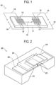
- FIG. 1 shows an example of a basic structure of a surface acoustic wave element including a piezoelectric element of an embodiment of the present disclosure.
- the surface acoustic wave element 10 includes a piezoelectric film 11, electrodes 12 on the piezoelectric film 11, a wiring 14 electrically connected to one electrode 12, and a wiring 15 electrically connected to another electrode 12.
- Each of the electrodes 12 may be a comb-shaped electrode (IDT).
- being electrically connected includes a case of being connected via "something having some electrical action.”
- the "something having some electrical action” is not particularly limited as long as it enables an exchange of an electric signal between connection targets.
- the "something having some electrical action” includes elements having various functions, such as an electrode, a wiring, a switching element, a resistance element, an inductor, a capacitive element, and the like.
- the piezoelectric film 11 is a single crystal piezoelectric film, which includes an aluminum nitride film, and a full width at half maximum (FWHM) at (002) diffraction peak of the aluminum nitride film may be smaller than 1.00 degree, specifically smaller than 0.50 degrees, more specifically smaller than 0.36 degrees. As the FWHM at (002) diffraction peak of the aluminum nitride film decreases, an orientation increases.
- the above-mentioned piezoelectric film 11 includes an aluminum nitride film having a crystal region that is highly oriented to a c-axis.
- An aluminum nitride film having a c-axis oriented-crystal region of a single crystal having high orientation and high crystallinity has few crystal grain boundaries. Therefore, when the piezoelectric film 11 includes the aluminum nitride film having the crystal region that is highly oriented to the c-axis, it is possible to suppress an attenuation of a surface acoustic wave due to the crystal grain boundaries.
- a surface acoustic wave element 10 that operates stably in a high-frequency region, has high piezoelectricity such as a low loss, a wide bandwidth, and a high propagation speed, and has a small temperature dependence.
- a resonance frequency of the surface acoustic wave element 10 (filter) and the like is determined by a distance between comb teeth of the electrode 12 (IDT).
- the film thickness of the aluminum nitride film contained in the piezoelectric film 11 may be, for example, 70 nm or more, specifically 100 nm or more.
- the piezoelectric film 11 may be a laminated film.
- the piezoelectric film 11 may have a laminated structure of an aluminum nitride film and one thin film selected from the group of a gallium nitride film, an aluminum gallium nitride film, an aluminum nitride film containing scandium, a silicon oxide film, and a thin film having a negative linear expansion coefficient on the aluminum nitride film.
- the film thickness of the thin film formed on the aluminum nitride film is not particularly limited as long as it does not hinder the high piezoelectricity and temperature dependence of the aluminum nitride film.
- gallium nitride film, aluminum gallium nitride film, and aluminum nitride film containing scandium are thin films having high piezoelectricity, it is possible to obtain a surface acoustic wave element 10 having higher piezoelectricity by laminating the above-described thin films with the aluminum nitride film having a crystal region that is highly oriented to the c-axis.
- Examples of materials having the negative linear expansion coefficient may include, but are not limited to, tungsten oxides such as Sc 2 W 3 O 12 (linear expansion coefficient near 25 degrees C: ⁇ 2.2 ⁇ 10 -6 /degrees C), Lu 2 W 3 O 12 (linear expansion coefficient near 25 degrees C: ⁇ 6,8 ⁇ 10 -6 /degrees C), and ZrW 2 O 8 (linear expansion coefficient near 25 degrees C: ⁇ 8,7 ⁇ 10 -6 /degrees C); manganese nitrides such as Mn 3 XN (X is Cu-Sn, Zn-Sn, etc., and maximum linear expansion coefficient: ⁇ 30 ⁇ 10 -6 /degrees C); aluminum oxides such as Al 2 O 3 ⁇ TiO 2 (linear expansion coefficient: ⁇ 0.8 ⁇ 10 -6 /degrees C) and Li 2 O ⁇ Al 2 O 3 ⁇ nSiO 2 (linear expansion coefficient: ⁇ 0.4 ⁇ 10 -6 /degrees C); LaCuFe 4 O 12 (having a huge negative linear expansion coefficient
- the piezoelectric film 11 may be a laminated film including the aluminum nitride film having a crystal region that is highly oriented to the c-axis, the thin film having high piezoelectricity (gallium nitride film, aluminum gallium nitride film, or aluminum nitride film containing scandium), and the thin film having excellent temperature stability (silicon oxide film or the thin film having a negative linear expansion coefficient).
- the piezoelectric film 11 having the above-described configuration, it is possible to obtain a surface acoustic wave element 10 having higher piezoelectricity and smaller temperature dependence.
- the aluminum nitride film that is highly oriented to the c-axis may be formed on a base substrate by a chemical vapor deposition (CVD) method or a molecular beam epitaxy (MBE) method. From the viewpoint of more highly orienting the crystal to the c-axis, the aluminum nitride film may be formed by using a metal organic chemical vapor deposition (MOCVD) method.
- CVD chemical vapor deposition
- MBE molecular beam epitaxy
- the aluminum nitride film that is highly oriented to the c-axis may be formed by the MOCVD method in which, for example, a nitrogen precursor gas and a group III element precursor gas are used as precursor gases, the base substrate is heated to 900 to 1,100 degrees C, the pressure at the time of film formation is 10 to 15 kPa, a film formation rate is 7 to 10 nm/min, and a V/III flow rate ratio (a rate of a flow rate ratio of the nitrogen precursor gas to a flow rate ratio of the group III element precursor gas) is 230 to 270.
- a nitrogen precursor gas and a group III element precursor gas are used as precursor gases
- the base substrate is heated to 900 to 1,100 degrees C
- the pressure at the time of film formation is 10 to 15 kPa
- a film formation rate is 7 to 10 nm/min
- a V/III flow rate ratio (a rate of a flow rate ratio of the nitrogen precursor gas to a flow rate ratio of the group III element precursor gas) is 230
- Examples of the above-mentioned nitrogen precursor gas may include ammonia and the like.
- Examples of the group III element precursor gas may include organometallic gases such as trimethylgallium (TMG), triethylgallium (TEG), trimethylindium (TMI), and trimethylaluminum (TMA).
- TMG trimethylgallium
- TOG triethylgallium
- TMI trimethylindium
- TMA trimethylaluminum
- the organometallic gas may supplied into a film-forming chamber in a state where it is mixed with a nitrogen gas or hydrogen gas as a carrier gas.
- a nitrogen gas or a hydrogen gas may be separately supplied into the film-forming chamber. Ammonia and trimethylaluminum may be used as the precursor gas.
- the crystallinity of the base substrate contributes to the crystallinity of the aluminum nitride film formed on the base substrate
- a base substrate having high crystallinity is used.
- the base substrate functions as a seed crystal of the aluminum nitride film, and the seed crystal may be used as a nucleus in crystal growth to form the aluminum nitride film having a crystal region that is highly oriented to the c-axis.
- the base substrate may include a silicon (111) substrate, an SOI substrate in which an active layer is silicon (111), a SiC substrate, a sapphire substrate, and the like. Since these substrates have the function as the above-mentioned seed crystal, it is possible to form the aluminum nitride film having a crystal region that is highly oriented to the c-axis.
- the following conditions may be applied because the aluminum nitride film having a crystal region that is highly oriented to the c-axis is easily obtained.
- impurities in a gas used for film formation are reduced.
- impurities contained in the film formation it is possible to suppress a collapse of the crystal state due to the impurities, and it becomes easy to obtain the aluminum nitride film having the crystal region that is highly oriented to the c-axis.
- the base substrate may be peeled from the piezoelectric film 11 by etching, grinding, polishing or the like, and another structure such as a substrate may be attached to the peeled surface of the piezoelectric film 11.
- a piezoelectric element such as a surface acoustic wave element including the piezoelectric film 11 may be easily mounted on another structure.
- Examples of the electrode 12 may include a laminated film of molybdenum, tungsten, platinum, and titanium, a laminated film of aluminum, gold, and chromium, and the like, which are formed by the sputtering method or the CVD method.
- Examples of the wiring 14 and the wiring 15 may include copper, silver, palladium, iridium, platinum, gold, and the like, which are formed by the sputtering method or a vacuum vapor deposition method.
- the piezoelectric element such as a high-performance surface acoustic wave element that operates stably in a high-frequency region, has high piezoelectricity, and has a small temperature dependence.
- FIG. 2 shows an example of a basic structure of a piezoelectric thin film resonance element including the piezoelectric element of the embodiment of the present disclosure.
- the piezoelectric thin film resonance element 20 includes a substrate 21, a lower electrode 22 on the substrate 21, a piezoelectric film 23 on the substrate 21 to cover a portion of the lower electrode 22, and an upper electrode 24 on the piezoelectric film 23.
- the piezoelectric film 23 is sandwiched between the lower electrode 22 and the upper electrode 24, and these are collectively referred to as a piezoelectric laminated structure.
- the piezoelectric film 23 causes longitudinal vibration in response to an high-frequency signal that is inputted, and the vibration causes resonance in the thickness direction of the piezoelectric film 23, resulting in resonance vibration (a bulk acoustic wave 25).
- the substrate 21 is a substrate to support the piezoelectric laminated structure (including the lower electrode 22, the piezoelectric film 23, and the upper electrode 24), and a lower part of the substrate 21 where the piezoelectric laminated structure is formed is hollow to freely vibrate the piezoelectric film 23 (the piezoelectric laminated structure).
- Examples of the substrate 21 may include a silicon (111) substrate, an SOI substrate in which an active layer is silicon (111), a SiC substrate, a sapphire substrate, and the like.
- an etching method or the like may be used as a method of forming the hollow in the substrate 21.
- the lower electrode 22 and the upper electrode 24 are electrodes configured to apply an electric field to the piezoelectric film 23.
- Examples of the lower electrode 22 and the upper electrode 24 may include a laminated film of molybdenum, tungsten, platinum, and titanium, a laminated film of aluminum, gold, and chromium, and the like, which are formed by the sputtering method or the CVD method.
- the piezoelectric film 23 is a single crystal piezoelectric film like the above-described piezoelectric film 11, and the single crystal piezoelectric film includes an aluminum nitride film having a crystal region that is highly oriented to the c-axis. Further, the piezoelectric film 23 may be a laminated film like the above-described piezoelectric film 11. The description of the piezoelectric film 11 may be invoked for details of a method of forming the piezoelectric film 23 and the like.
- the aluminum nitride film having the c-axis oriented crystal region of a single crystal having high orientation and high crystallinity has few crystal defects and grain boundaries. Therefore, when the piezoelectric film 23 includes the aluminum nitride film having the crystal region that is highly oriented to the c-axis, it is possible to suppress attenuation of a bulk acoustic wave due to crystal defects and crystal grain boundaries. Therefore, it is possible to obtain a piezoelectric thin film resonance element 20 that operates stably in the high-frequency region, has high piezoelectricity such as a low loss, a wide bandwidth, and a high propagation speed, and has a small temperature dependence.
- the piezoelectric element such as a high-performance piezoelectric thin film resonance element that operates stably in the high frequency region, has high piezoelectricity, and has a small temperature dependence.
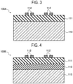
- a surface acoustic wave element 100A shown in FIG. 3 includes a base substrate 110, a piezoelectric film 111 on the base substrate 110, and comb-shaped electrodes 112 on the piezoelectric film 111.
- the piezoelectric film 111 includes an aluminum nitride film having a crystal region that is highly oriented to the c-axis.
- the base substrate 110 having high crystallinity functions as a seed crystal of the aluminum nitride film, and the seed crystal may be used as a nucleus for crystal growth to form the aluminum nitride film having the crystal region that is highly oriented to the c-axis.
- the description of the piezoelectric film 11 may be invoked for details of physical characteristics of the piezoelectric film 111, a method of forming the piezoelectric film 111, and the like.
- the description of the electrode 12 may be invoked for the comb-shaped electrode 112.
- the base substrate 110 has a linear expansion coefficient smaller than that of the piezoelectric film 111. Therefore, the surface acoustic wave element 100A including the base substrate 110 and the piezoelectric film 111 has excellent temperature stability.
- the piezoelectric film 111 including the aluminum nitride film having the crystal region that is highly oriented to the c-axis but also the action of the base substrate 110 having a small linear expansion coefficient, it is possible to obtain the surface acoustic wave element 100A having high piezoelectricity and smaller temperature dependence.
- a surface acoustic wave element 100B shown in FIG. 4 includes a substrate 115, a silicon oxide film 113 on the substrate 115, a piezoelectric film 111 on the silicon oxide film 113, and a comb-shaped electrode 112 on the piezoelectric film 111.
- a difference between the surface acoustic wave element 100B and the surface acoustic wave element 100A is that the substrate 115 on which the silicon oxide film 113 is formed is provided instead of the base substrate 110.
- the surface acoustic wave element 100B may be manufactured by forming the piezoelectric film 111 by using the base substrate 110 in the surface acoustic wave element 100A, peeling the base substrate 110 from the piezoelectric film 111 by etching, grinding, polishing, or the like, and attaching the substrate 115 on which the silicon oxide film 113 is formed to the peeled surface of the piezoelectric film 111.
- the silicon oxide film 113 has a small linear expansion coefficient. Therefore, the surface acoustic wave element 100B including the silicon oxide film 113 and the piezoelectric film 111 has excellent temperature stability. By not only the action of the piezoelectric film 111 including the aluminum nitride film having the crystal region that is highly oriented to the c-axis, but also the action of the silicon oxide film 113 having a small linear expansion coefficient, it is possible to obtain the surface acoustic wave element 100B having high piezoelectricity and smaller temperature dependence.
- a surface acoustic wave element 100C shown in FIG. 5 includes a base substrate 110, a piezoelectric film 111 on the base substrate 110, a comb-shaped electrode 112 on the piezoelectric film 111, an adhesive 114 on the piezoelectric film 111, and a substrate 120 on the adhesive 114.
- a difference between the surface acoustic wave element 100C and the surface acoustic wave element 100A is that the adhesive 114 and the substrate 120 are further provided.
- the substrate 120 functions as an auxiliary substrate.
- the substrate 120 is formed with a hollow and is adhered to the piezoelectric film 111 via the adhesive 114.
- An atmosphere of the hollow formed in the substrate 120 is filled with vacuum or an inert gas such as nitrogen. Further, the substrate 120 does not come into contact with the comb-shaped electrode 112. Examples of the substrate 120 may include a silicon substrate and a glass substrate.
- the adhesive 114 is not particularly limited as long as it can adhere the piezoelectric film 111 to the substrate 120, and may use, for example, an epoxy resin.
- the substrate 120 has a small linear expansion coefficient. Therefore, the surface acoustic wave element 100C including the substrate 120 and the piezoelectric film 111 may suppress elongation in the lateral direction (a direction perpendicular to the thickness direction of the piezoelectric film 111) at a high temperature, and thus has excellent temperature stability.
- the piezoelectric film 111 including the aluminum nitride film having the crystal region that is highly oriented to the c-axis but also the action of the substrate 120 having the small linear expansion coefficient, it is possible to obtain the surface acoustic wave element 100C having high piezoelectricity and smaller temperature dependence.
- a surface acoustic wave element 100D shown in FIG. 6 includes an SOI substrate 130, a piezoelectric film 111 on the SOI substrate 130, and a comb-shaped electrode 112 on the piezoelectric film 111.
- a difference between the surface acoustic wave element 100D and the surface acoustic wave element 100A is that the SOI substrate 130 is provided in place of the base substrate 110. Since the surface acoustic wave element 100D includes the piezoelectric film 111 which is a piezoelectric thin film, it is also referred to as a thin film acoustic wave element.
- the SOI substrate 130 includes a silicon film 131, a silicon oxide film 132, and an active layer 133 which is silicon (111).
- the silicon film 131 is formed with an opening, and the back surface of the silicon oxide film 132 is exposed. The opening may be formed by etching the silicon film 131.
- the silicon oxide film 132 has a small linear expansion coefficient. Therefore, the surface acoustic wave element 100D including the silicon oxide film 132 has excellent temperature stability.
- the active layer 133 having high crystallinity functions as a seed crystal of the aluminum nitride film, and the seed crystal may be used as a nucleus for crystal growth to form an aluminum nitride film having a crystal region that is highly oriented to the c-axis.
- the surface acoustic wave element 100D has excellent temperature stability.
- the piezoelectric film 111 including the aluminum nitride film having a crystal region that is highly oriented to the c-axis but also the action of the SOI substrate 130, it is possible to obtain the surface acoustic wave element 100D having high piezoelectricity and smaller temperature dependence.
- a surface acoustic wave element 100E shown in FIG. 7 includes an SOI substrate 130, a piezoelectric film 111 on the SOI substrate 130, and a comb-shaped electrode 112 on the piezoelectric film 111.
- a difference between the surface acoustic wave element 100E and the surface acoustic wave element 100D is that the back surface of the active layer 133 in the SOI substrate 130 is exposed.
- the surface acoustic wave element 100E is a thin film surface acoustic wave element.
- the surface acoustic wave element 100E has excellent temperature stability.
- the piezoelectric film 111 including the aluminum nitride film having a crystal region that is highly oriented to the c-axis but also the action of the SOI substrate 130, it is possible to obtain the surface acoustic wave element 100E having high piezoelectricity and smaller temperature dependence.
- a surface acoustic wave element 100F shown in FIG. 8 includes an SOI substrate 140, a piezoelectric film 111 on the SOI substrate 140, a comb-shaped electrode 112 on the piezoelectric film 111, and a substrate 120 on the piezoelectric film 111.
- a difference between the surface acoustic wave element 100F and the surface acoustic wave element 100D is that the substrate 120 is provided.
- the surface acoustic wave element 100E is a thin film acoustic wave element.
- the SOI substrate 140 includes a silicon film 141, a silicon oxide film 142, and an active layer 143 which is silicon (111).
- the description of the silicon film 131, the silicon oxide film 132, and the active layer 133 which is silicon (111) may be invoked for the silicon film 141, the silicon oxide film 142, and the active layer 143 which is silicon (111).
- the piezoelectric film 111 and the substrate 120 are adhered to each other and may be adhered to each other by using, for example, the above-mentioned adhesive 114.
- the surface acoustic wave element 100F has excellent temperature stability.
- the piezoelectric film 111 including the aluminum nitride film having a crystal region that is highly oriented to the c-axis but also the action of the substrate 120 and the SOI substrate 130, it is possible to obtain the surface acoustic wave element 100F having high piezoelectricity and smaller temperature dependence.
- a surface acoustic wave element 100G shown in FIG. 9 includes a base substrate 110, a piezoelectric film 111 on the base substrate 110, a piezoelectric film 150 on the piezoelectric film 111, and a comb-shaped electrode 112 on the piezoelectric film 150.
- a difference between the surface acoustic wave element 100G and the surface acoustic wave element 100A is that the piezoelectric film 150 is further provided.
- the piezoelectric film 150 is an aluminum nitride film containing scandium formed by the sputtering method.
- the piezoelectric film 150 may be an aluminum nitride film containing 0.5 to 35 atom% of scandium. Since the aluminum nitride film containing scandium has high piezoelectricity, by laminating it with the aluminum nitride film having a crystal region that is highly oriented to the c-axis, it is possible to obtain the surface acoustic wave element 100G having higher piezoelectricity.
- a surface acoustic wave element 100H shown in FIG. 10 includes a base substrate 110, a piezoelectric film 111 on the base substrate 110, a piezoelectric film 150 on the piezoelectric film 111, and a comb-shaped electrode 112 on the piezoelectric film 150.
- a difference between the surface acoustic wave element 100H and the surface acoustic wave element 100G is that the back surface of the piezoelectric film 111 is exposed.
- a high piezoelectricity may be provided by laminating the aluminum nitride film having a crystal region that is highly oriented to the c-axis with the aluminum nitride film containing scandium, and thus it is possible to obtain the surface acoustic wave element 100H having higher piezoelectricity.
- a piezoelectric thin film resonance element 200A shown in FIG. 11 includes a base substrate 210, a lower electrode 211 on the base substrate 210, a piezoelectric film 213 on the lower electrode 211, and an upper electrode 214 on the piezoelectric film 213.
- the upper electrode 214 is electrically connected to the lower electrode 211 via a wiring 224.
- the description of the base substrate described in the above-described surface acoustic wave element may be invoked for the base substrate 210.
- the piezoelectric film 213 includes an aluminum nitride film having a crystal region that is highly oriented to the c-axis.
- the base substrate 210 having high crystallinity functions as a seed crystal of the aluminum nitride film, and the seed crystal may be used as a nucleus for crystal growth to form an aluminum nitride film having a crystal region that is highly oriented to the c-axis.
- the description of the piezoelectric film 11 may be invoked for details of physical characteristics of the piezoelectric film 213, a method of forming the piezoelectric film 213, and the like.
- the description of the lower electrode 22 may be invoked for the lower electrode 211.
- the lower electrode 211 containing silicon may be used.
- a silicon substrate obtained by a high-concentration doping to give conductivity may be used as the lower electrode 211.
- the description of the upper electrode 24 may be invoked for the upper electrode 214.
- the lower electrode 211 has a small linear expansion coefficient. Therefore, the piezoelectric thin film resonance element 200A including the lower electrode 211 and the piezoelectric film 213 has excellent temperature stability. By not only the action of the piezoelectric film 213 including the aluminum nitride film having a crystal region that is highly oriented to the c-axis, but also the action of the lower electrode 211 having a small linear expansion coefficient, it is possible to obtain the piezoelectric thin film resonance element 200A having high piezoelectricity and smaller temperature dependence.
- a piezoelectric thin film resonance element 200B shown in FIG. 12 includes a base substrate 210, a silicon oxide film 215 on the base substrate 210, a lower electrode 211 on the silicon oxide film 215, a piezoelectric film 213 on the lower electrode 211, and an upper electrode 214 on the piezoelectric film 213.
- a difference between the piezoelectric thin film resonance element 200B and the piezoelectric thin film resonance element 200A is that the silicon oxide film 215 is provided.
- the silicon oxide film 215 has a small linear expansion coefficient. Therefore, the piezoelectric thin film resonance element 200B including the silicon oxide film 215 and the piezoelectric film 213 has excellent temperature stability. By not only the action of the piezoelectric film 213 including the aluminum nitride film having a crystal region that is highly oriented to the c-axis, but also the action of the silicon oxide film 215 having a small linear expansion coefficient, it is possible to obtain the piezoelectric thin film resonance element 200B having high piezoelectricity and smaller temperature dependence.
- a piezoelectric thin film resonance element 200C shown in FIG. 13 includes a base substrate 210, a lower electrode 211, a piezoelectric film 213, an upper electrode 214, and a silicon oxide film 216.
- a difference between the piezoelectric thin film resonance element 200C and the piezoelectric thin film resonance element 200A is that the silicon oxide film 216 is provided. That is, the difference is that the silicon oxide film 216 is sandwiched between the lower electrode 211 and the upper electrode 214.
- the silicon oxide film 216 has a small linear expansion coefficient. Therefore, the piezoelectric thin film resonance element 200C including the silicon oxide film 216 and the piezoelectric film 213 has excellent temperature stability. By not only the action of the piezoelectric film 213 including the aluminum nitride film having the crystal region that is highly oriented to the c-axis, but also the action of the silicon oxide film 216 having a small linear expansion coefficient, it is possible to obtain the piezoelectric thin film resonance element 200C having high piezoelectricity and smaller temperature dependence.
- a piezoelectric thin film resonance element 200D shown in FIG. 14 includes a base substrate 210, a lower electrode 211, a piezoelectric film 213, an upper electrode 214, and a silicon film 217.
- a difference between the piezoelectric thin film resonance element 200D and the piezoelectric thin film resonance element 200C is that the silicon film 217 is provided in place of the silicon oxide film 216.
- the silicon film 217 functions as a seed crystal of the aluminum nitride film, and the seed crystal may be used as a nucleus for crystal growth to form an aluminum nitride film having a crystal region that is highly oriented to the c-axis.
- the piezoelectric film 213 including the aluminum nitride film having the crystal region that is highly oriented to the c-axis it is possible to obtain the piezoelectric thin film resonance element 200D having high piezoelectricity and small temperature dependence.
- a piezoelectric thin film resonance element 200E shown in FIG. 15 includes a base substrate 210, a piezoelectric film 213 on the base substrate 210, a piezoelectric film 250 on the piezoelectric film 213, a lower electrode 211, and an upper electrode 214.
- a difference between the piezoelectric thin film resonance element 200E and the piezoelectric thin film resonance element 200C is that the piezoelectric film 250 is provided in place of the silicon oxide film 216.
- the piezoelectric film 250 is an aluminum nitride film containing scandium formed by the sputtering method.
- the piezoelectric film 250 may be an aluminum nitride film containing 0.5 to 35 atom% of scandium. Since the aluminum nitride film containing scandium has high piezoelectricity, high piezoelectricity may be provided by laminating it with the aluminum nitride film having a crystal region that is highly oriented to the c-axis, and thus, it is possible to obtain the piezoelectric thin film resonance element 200E having higher piezoelectricity.
- a method for manufacturing a piezoelectric film used in this Example is shown below.
- a silicon (111) substrate as a base substrate is provided, and an aluminum nitride film as a piezoelectric film is formed on the silicon (111) substrate by a MOCVD method.
- a film-forming condition is as follows.
- Aluminum nitride films which are four types of Samples with different film thicknesses, are formed under the above-mentioned film-forming condition.
- a film thickness of the formed aluminum nitride film of Sample 1 is 34.4 nm
- a film thickness of the aluminum nitride film of Sample 2 is 69.3 nm
- a film thickness of the aluminum nitride film of Sample 3 is 105.0 nm
- a film thickness of the aluminum nitride film of Sample 4 is 196.0 nm.
- Sample 5 in which a gallium nitride film is formed on the aluminum nitride film of Sample 4 is also provided.
- a film-forming condition for the gallium nitride film is as follows.
- X-ray diffraction is performed on Samples 1 to 5 to evaluate the crystal state.
- the XRD used is one manufactured by Malvern Panalytical Company. A condition is that in ⁇ scanning, a scanning range is 5 degrees (measured at ⁇ 2.5 degrees centered at the angle at which the maximum value is obtained), and a step width is 0.01 degrees, and a scanning speed is 1.5 degrees/min.
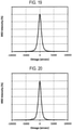
- FIG. 16 shows an XRD spectrum at (002) diffraction peak of Sample 1
- FIG. 17 shows an XRD spectrum at (002) diffraction peak of Sample 2
- FIG. 18 shows an XRD spectrum at (002) diffraction peak of Sample 3
- FIG. 19 shows an XRD spectrum at (002) diffraction peak of Sample 4
- FIG. 20 shows an XRD spectrum at (002) diffraction peak of Sample 5, respectively.
- the vertical axis represents XRD integrity (%) and the horizontal axis represents Omega (arcsec).
- an FWHM at (002) diffraction peak of Sample 1 was 1.007 degrees.
- an FWHM at (002) diffraction peak of Sample 2 was 0.641 degrees.
- an FWHM at (002) diffraction peak of Sample 3 was 0.493 degrees.
- an FWHM at (002) diffraction peak of Sample 4 was 0.353 degrees.
- an FWHM at (002) diffraction peak of sample 5 was 0.334 degrees.
- the film thickness of the aluminum nitride film is equal to or larger than the film thickness of the aluminum nitride film of Sample 2, for example, 70 nm or more
- the XRD spectrum at (002) diffraction peak has a sharp peak shape
- the FWHM at the (002) diffraction peak also becomes smaller than 1.00 degree.
- the film thickness of the aluminum nitride film is 100 nm or more
- the XRD spectrum at the (002) diffraction peak has a sharper peak shape, and the FWHM at (002) diffraction peak also becomes smaller than 0.50 degrees.
- the XRD spectrum at (002) diffraction peak has a sharper peak shape due to the action of the gallium nitride film, and the FWHM at (002) diffraction peak also becomes smaller.
- a high-performance piezoelectric element that operates stably in a high-frequency region, has high piezoelectricity, and has small temperature dependence. Further, it is possible to provide a surface acoustic wave element including the piezoelectric element. Further, it is possible to provide a piezoelectric thin film resonance element including the piezoelectric element. Further, it is possible to provide a method of manufacturing the piezoelectric element.
Landscapes
- Chemical & Material Sciences (AREA)
- Acoustics & Sound (AREA)
- Physics & Mathematics (AREA)
- Engineering & Computer Science (AREA)
- Crystallography & Structural Chemistry (AREA)
- Materials Engineering (AREA)
- Metallurgy (AREA)
- Organic Chemistry (AREA)
- Manufacturing & Machinery (AREA)
- Ceramic Engineering (AREA)
- Chemical Kinetics & Catalysis (AREA)
- General Chemical & Material Sciences (AREA)
- Inorganic Chemistry (AREA)
- Piezo-Electric Or Mechanical Vibrators, Or Delay Or Filter Circuits (AREA)
- Surface Acoustic Wave Elements And Circuit Networks Thereof (AREA)
- Formation Of Insulating Films (AREA)
Abstract
Description
- This application is based upon and claims the benefit of priority from
Japanese Patent Application No. 2020-157233, filed on September 18, 2020 - The present disclosure relates to a piezoelectric element, a method of manufacturing the same, a surface acoustic wave element, and a piezoelectric thin film resonance element.
- Portable devices such as smartphones for which miniaturization and power saving are strongly required are rapidly expanding in use, and in wireless communication systems for portable devices, devices that utilize high frequencies in the GHz band are being actively developed. In a high-frequency circuit used in these wireless communication systems, an IF (Intermediate Frequency) filter and an RF (Radio Frequency) filter are used in an analog circuit part.
- The above-mentioned filters are used to pass only a signal of a desired frequency band and block signals of other frequencies. For example, the RF filter includes a plurality of resonance elements, and a desired filter band is formed by a ladder circuit in which the resonance elements are connected in a ladder shape.
- A specific example of the filter may include a SAW filter which is a filter in which a surface acoustic wave resonator (SAWR) as a piezoelectric element is used. The SAW filter is approaching the limit of improvement in characteristics as the frequency to be used is increased. As an alternative to the SAW filter, an FBAR (Film Bulk Acoustic Resonator) filter, which is a filter where a piezoelectric thin film resonance element (also referred to as an FBAR) as a piezoelectric element is used, has been developed.
- The SAW filter and the FBAR filter include a piezoelectric film. In the SAW filter, a comb-shaped electrode (also referred to as an interdigital transducer (IDT)) is formed on the surface of the piezoelectric film, and a band of the filter is formed by using the resonance characteristics of a surface acoustic wave excited by the IDT. In the FBAR filter, the piezoelectric film is sandwiched between upper and lower electrodes, and longitudinal vibration in the film thickness direction is used.
- Piezoelectric film materials for the piezoelectric element may include aluminum nitride (AlN), zinc oxide (ZnO), lithium niobate (LiNbO3), lithium tantalate (LiTaO3), and lead zirconate titanate (Pb(Zr,Ti)O3: PZT), and the like. A filter in the high-frequency band is required to have a wide bandwidth, a high propagation speed, and temperature stability, and the piezoelectric film is required to use a material having a high piezoelectric constant, a high propagation speed, and a small temperature coefficient.
- Regarding the above requirements, it is known that aluminum nitride is preferable as a piezoelectric film material for a piezoelectric element of a filter in a high-frequency band.
- In the related art, it is known that a piezoelectric thin film resonator having high characteristics and high performance may be obtained by adding an alkaline earth metal and/or a rare earth element to an aluminum nitride thin film.
- However, although aluminum nitride formed by a sputtering method may be easily thinned and thus tends to have a high frequency, it has many crystal grain boundaries. A crystal grain boundary is a boundary among a large number of crystals (polycrystals) existing in a thin film and is a lattice defect in which atoms are arranged discontinuously. Although the grain boundary, which is an origin of various functions of a material due to its specific atomic arrangement, exists only in an extremely small region with a width of several nanometers, it may often determine an overall performance of materials and elements. For example, the crystal grain boundary may greatly reduce a thermal conductivity and a vibration propagation of a material.
- An embodiment of the present disclosure provides a high-performance piezoelectric element that operates stably in a high-frequency region, has a high piezoelectric property, and has small temperature dependence. Further, another embodiment of the present disclosure provides a surface acoustic wave element including the piezoelectric element. Further, another embodiment of the present disclosure provides a piezoelectric thin film resonance element including the piezoelectric element. Further, another embodiment of the present disclosure provides a method of manufacturing the piezoelectric element.
- According to an embodiment of the present disclosure, there is provided a piezoelectric element in which a single crystal piezoelectric film including an aluminum nitride film that is highly oriented on a c-axis is used. Aspects of the present embodiment are as follows.
- According to an aspect of the present embodiment, there is provided a piezoelectric element including: a single crystal piezoelectric film, wherein the single crystal piezoelectric film includes an aluminum nitride film, and a full width at half maximum at the (002) diffraction peak of the aluminum nitride film is smaller than 1.00 degree.
- According to another aspect of the present embodiment, there is provided a piezoelectric element including: a base substrate; and a single crystal piezoelectric film on the base substrate, wherein the single crystal piezoelectric film includes an aluminum nitride film, and a full width at half maximum at the (002) diffraction peak of the aluminum nitride film is smaller than 1.00 degree.
- According to another aspect of the present embodiment, there is provided a surface acoustic wave element including the above-mentioned piezoelectric element.
- According to another aspect of the present embodiment, there is provided a piezoelectric thin film resonance element including the above-mentioned piezoelectric element.
- According to another aspect of the present embodiment, there is provided a method of manufacturing a piezoelectric element, including: forming a single crystal piezoelectric film including an aluminum nitride film on a base substrate, wherein the aluminum nitride film is formed by one selected from the group of a CVD method and a MBE method, and a full width at half maximum at the (002) diffraction peak of the aluminum nitride film is smaller than 1.00 degree.
-
-
FIG. 1 is a view to explain a basic structure of a surface acoustic wave element. -
FIG. 2 is a view to explain a basic structure of a piezoelectric thin film resonance element. -
FIG. 3 is a cross-sectional view to explain a surfaceacoustic wave element 100A according to an embodiment of the present disclosure. -
FIG. 4 is a cross-sectional view to explain a surfaceacoustic wave element 100B according to an embodiment of the present disclosure. -
FIG. 5 is a cross-sectional view to explain a surfaceacoustic wave element 100C according to an embodiment of the present disclosure. -
FIG. 6 is a cross-sectional view to explain a surfaceacoustic wave element 100D according to an embodiment of the present disclosure. -
FIG. 7 is a cross-sectional view to explain a surfaceacoustic wave element 100E according to an embodiment of the present disclosure. -
FIG. 8 is a cross-sectional view to explain a surfaceacoustic wave element 100F according to an embodiment of the present disclosure. -
FIG. 9 is a cross-sectional view to explain a surfaceacoustic wave element 100G according to an embodiment of the present disclosure. -
FIG. 10 is a cross-sectional view to explain a surfaceacoustic wave element 100H according to an embodiment of the present disclosure. -
FIG. 11 is a cross-sectional view to explain a piezoelectric thinfilm resonance element 200A according to an embodiment of the present disclosure. -
FIG. 12 is a cross-sectional view to explain a piezoelectric thinfilm resonance element 200B according to an embodiment of the present disclosure. -
FIG. 13 is a cross-sectional view to explain a piezoelectric thinfilm resonance element 200C according to an embodiment of the present disclosure. -
FIG. 14 is a cross-sectional view to explain a piezoelectric thinfilm resonance element 200D according to an embodiment of the present disclosure. -
FIG. 15 is a cross-sectional view to explain a piezoelectric thinfilm resonance element 200E according to an embodiment of the present disclosure. -
FIG. 16 is a graph showing an XRD spectrum at the (002) diffraction peak of Sample 1 in an Example. -
FIG. 17 is a graph showing an XRD spectrum at the (002) diffraction peak of Sample 2 in an Example. -
FIG. 18 is a graph showing an XRD spectrum at the (002) diffraction peak of Sample 3 in the Example. -
FIG. 19 is a graph showing an XRD spectrum at the (002) diffraction peak of Sample 4 in the Example. -
FIG. 20 is a graph showing an XRD spectrum at the (002) diffraction peak of Sample 5 in the Example. - Embodiments of the present disclosure will be now described with reference to the drawings. In the description of the drawings described below, the same or similar parts are denoted by the same or similar reference numerals. However, it should be noted that the drawings are schematic and a relationship between a thickness and a planar dimension of each component is different from the actual one. Therefore, a specific thickness and dimension should be determined in consideration of the following description. In addition, it goes without saying that parts of the drawings having different dimensional relationships and ratios are included.
- Further, the embodiments shown below exemplify apparatuses and methods to embody technical ideas, and do not specify a material, a shape, a structure, an arrangement, and the like of each component. The present embodiment may be modified in various ways within the scope of the claims.
- An aspect of the present embodiment is as follows.
- <1> A piezoelectric element including: a single crystal piezoelectric film, wherein the single crystal piezoelectric film includes an aluminum nitride film, and wherein a full width at half maximum at (002) diffraction peak of the aluminum nitride film is smaller than 1.00 degree.
- <2> A piezoelectric element including: a base substrate; and a single crystal piezoelectric film on the base substrate, wherein the single crystal piezoelectric film includes an aluminum nitride film, and wherein a full width at half maximum at (002) diffraction peak of the aluminum nitride film is smaller than 1.00 degree.
- <3> The piezoelectric element of <2>, wherein the base substrate is one selected from the group of a silicon (111) substrate, an SOI substrate in which an active layer is silicon (111), a SiC substrate, and a sapphire substrate.
- <4> The piezoelectric element of any one of <1> to <3>, wherein the full width at half maximum at (002) diffraction peak of the aluminum nitride film is smaller than 0.36 degrees.
- <5> The piezoelectric element of any one of <1> to <4>, wherein a film thickness of the aluminum nitride film is 70 nm or more.
- <6> The piezoelectric element of any one of <1> to <5>, wherein a film thickness of the aluminum nitride film is 100 nm or more.
- <7> The piezoelectric element of any one of <1> to <6>, wherein the single crystal piezoelectric film is a laminated film, wherein the laminated film includes a thin film on the aluminum nitride film, and wherein the thin film is at least one selected from the group of a gallium nitride film, an aluminum gallium nitride film, an aluminum nitride film containing scandium, a silicon oxide film, and a thin film having a negative linear expansion coefficient.
- <8> A surface acoustic wave element including the piezoelectric element of any one of <1> to <7>.
- <9> A piezoelectric thin film resonance element including the piezoelectric element of any one of <1> to <7>.
- <10> A method of manufacturing a piezoelectric element, including: forming a single crystal piezoelectric film including an aluminum nitride film on a base substrate, wherein the aluminum nitride film is formed by one selected from the group of a CVD method and a MBE method, and wherein a full width at half maximum at (002) diffraction peak of the aluminum nitride film is smaller than 1.00 degree.
- <11> The method of <10>, wherein the base substrate is one selected from the group of a silicon (111) substrate, an SOI substrate in which an active layer is silicon (111), a SiC substrate, and a sapphire substrate.
- <12> The method of <10> or <11>, wherein the aluminum nitride film is formed by a MOCVD method.
- <13> The method of <12>, wherein the aluminum nitride film is formed by the MOCVD method in which trimethylaluminum and ammonia are used, the base substrate is set at 900 to 1,100 degrees C, and a pressure at the time of film formation is 10 to 15 kPa.
- <14> The method of any one of <10> to <13>, wherein the full width at half maximum at (002) diffraction peak of the aluminum nitride film is smaller than 0.36 degrees.
- <15> The method of any one of <10> to <14>, wherein a film thickness of the aluminum nitride film is 70 nm or more.
- <16> The method of any one of <10> to <15>, wherein a film thickness of the aluminum nitride film is 100 nm or more.
- <17> The method of any one of <10> to <16>, wherein the single crystal piezoelectric film is a laminated film, wherein the laminated film forms a thin film on the aluminum nitride film, and wherein the thin film is at least one selected from the group of a gallium nitride film, an aluminum gallium nitride film, an aluminum nitride film containing scandium, a silicon oxide film, and a thin film having a negative linear expansion coefficient.
- <18> The method of any one of <10> to <17>, wherein the base substrate is peeled off by at least one selected from the group of etching, grinding, and polishing.
- A piezoelectric element according to an embodiment of the present disclosure will be described.
- The piezoelectric element of the embodiment includes at least a single crystal piezoelectric film, and specific use of the piezoelectric element is not particularly limited. For example, the piezoelectric element may be used for a SAW filter, an FBAR filter, and the like.
- Here, a surface acoustic wave element used in the SAW filter and a piezoelectric thin film resonance element used in the FBAR filter will be described with reference to the drawings.
-
FIG. 1 shows an example of a basic structure of a surface acoustic wave element including a piezoelectric element of an embodiment of the present disclosure. - The surface
acoustic wave element 10 includes apiezoelectric film 11,electrodes 12 on thepiezoelectric film 11, awiring 14 electrically connected to oneelectrode 12, and awiring 15 electrically connected to anotherelectrode 12. Each of theelectrodes 12 may be a comb-shaped electrode (IDT). When a signal is input from the outside to the one electrode 12 (IDT) formed on the surface of thepiezoelectric film 11 via thewiring 14, a surfaceacoustic wave 13 excited by the oneelectrode 12 propagates through the anotherelectrode 12 and a signal is output to the outside via thewiring 15. - In the present disclosure and the like, "being electrically connected" includes a case of being connected via "something having some electrical action." Here, the "something having some electrical action" is not particularly limited as long as it enables an exchange of an electric signal between connection targets. For example, the "something having some electrical action" includes elements having various functions, such as an electrode, a wiring, a switching element, a resistance element, an inductor, a capacitive element, and the like.
- The
piezoelectric film 11 is a single crystal piezoelectric film, which includes an aluminum nitride film, and a full width at half maximum (FWHM) at (002) diffraction peak of the aluminum nitride film may be smaller than 1.00 degree, specifically smaller than 0.50 degrees, more specifically smaller than 0.36 degrees. As the FWHM at (002) diffraction peak of the aluminum nitride film decreases, an orientation increases. - The above-mentioned
piezoelectric film 11 includes an aluminum nitride film having a crystal region that is highly oriented to a c-axis. An aluminum nitride film having a c-axis oriented-crystal region of a single crystal having high orientation and high crystallinity has few crystal grain boundaries. Therefore, when thepiezoelectric film 11 includes the aluminum nitride film having the crystal region that is highly oriented to the c-axis, it is possible to suppress an attenuation of a surface acoustic wave due to the crystal grain boundaries. Therefore, it is possible to obtain a surfaceacoustic wave element 10 that operates stably in a high-frequency region, has high piezoelectricity such as a low loss, a wide bandwidth, and a high propagation speed, and has a small temperature dependence. - Further, a resonance frequency of the surface acoustic wave element 10 (filter) and the like is determined by a distance between comb teeth of the electrode 12 (IDT).
- Further, from the viewpoint of high orientation, the film thickness of the aluminum nitride film contained in the
piezoelectric film 11 may be, for example, 70 nm or more, specifically 100 nm or more. Thepiezoelectric film 11 may be a laminated film. Specifically, thepiezoelectric film 11 may have a laminated structure of an aluminum nitride film and one thin film selected from the group of a gallium nitride film, an aluminum gallium nitride film, an aluminum nitride film containing scandium, a silicon oxide film, and a thin film having a negative linear expansion coefficient on the aluminum nitride film. The film thickness of the thin film formed on the aluminum nitride film is not particularly limited as long as it does not hinder the high piezoelectricity and temperature dependence of the aluminum nitride film. - Since the above-mentioned gallium nitride film, aluminum gallium nitride film, and aluminum nitride film containing scandium are thin films having high piezoelectricity, it is possible to obtain a surface
acoustic wave element 10 having higher piezoelectricity by laminating the above-described thin films with the aluminum nitride film having a crystal region that is highly oriented to the c-axis. - Further, by laminating the silicon oxide film having excellent temperature stability and the thin film having the negative linear expansion coefficient with the aluminum nitride film having a crystal region that is highly oriented to the c-axis, it is possible to obtain a surface
acoustic wave element 10 having a smaller temperature dependence. - Examples of materials having the negative linear expansion coefficient may include, but are not limited to, tungsten oxides such as Sc2W3O12 (linear expansion coefficient near 25 degrees C: ―2.2×10⁻⁶/degrees C), Lu2W3O12 (linear expansion coefficient near 25 degrees C: ―6,8×10⁻⁶/degrees C), and ZrW2O8 (linear expansion coefficient near 25 degrees C: ―8,7×10⁻⁶/degrees C); manganese nitrides such as Mn3XN (X is Cu-Sn, Zn-Sn, etc., and maximum linear expansion coefficient: ―30×10-6/degrees C); aluminum oxides such as Al2O3·TiO2 (linear expansion coefficient: ―0.8×10⁻⁶/degrees C) and Li2O·Al2O3·nSiO2 (linear expansion coefficient: ―0.4×10⁻⁶/degrees C); LaCuFe4O12 (having a huge negative linear expansion coefficient of -1% from the linear expansion coefficient before the phase transition due to a phase transition near 120 degrees C); ruthenium oxides having a layered perovskite structure such as Ca2RuO3.74 (linear expansion coefficient at -138 to 72 degrees C: ―115×10-6/degrees C); and samarium yttrium sulfides, which are rare earth sulfides, such as Sm0.78Y0.22S (linear expansion coefficient at -173 to 42 degrees C: ―65×10-6/degrees C).
- Further, the
piezoelectric film 11 may be a laminated film including the aluminum nitride film having a crystal region that is highly oriented to the c-axis, the thin film having high piezoelectricity (gallium nitride film, aluminum gallium nitride film, or aluminum nitride film containing scandium), and the thin film having excellent temperature stability (silicon oxide film or the thin film having a negative linear expansion coefficient). By using thepiezoelectric film 11 having the above-described configuration, it is possible to obtain a surfaceacoustic wave element 10 having higher piezoelectricity and smaller temperature dependence. - The aluminum nitride film that is highly oriented to the c-axis may be formed on a base substrate by a chemical vapor deposition (CVD) method or a molecular beam epitaxy (MBE) method. From the viewpoint of more highly orienting the crystal to the c-axis, the aluminum nitride film may be formed by using a metal organic chemical vapor deposition (MOCVD) method.
- The aluminum nitride film that is highly oriented to the c-axis may be formed by the MOCVD method in which, for example, a nitrogen precursor gas and a group III element precursor gas are used as precursor gases, the base substrate is heated to 900 to 1,100 degrees C, the pressure at the time of film formation is 10 to 15 kPa, a film formation rate is 7 to 10 nm/min, and a V/III flow rate ratio (a rate of a flow rate ratio of the nitrogen precursor gas to a flow rate ratio of the group III element precursor gas) is 230 to 270.
- Examples of the above-mentioned nitrogen precursor gas may include ammonia and the like. Examples of the group III element precursor gas may include organometallic gases such as trimethylgallium (TMG), triethylgallium (TEG), trimethylindium (TMI), and trimethylaluminum (TMA). The organometallic gas may supplied into a film-forming chamber in a state where it is mixed with a nitrogen gas or hydrogen gas as a carrier gas. In addition to these precursor gases, a nitrogen gas or a hydrogen gas may be separately supplied into the film-forming chamber. Ammonia and trimethylaluminum may be used as the precursor gas.
- Further, since the crystallinity of the base substrate contributes to the crystallinity of the aluminum nitride film formed on the base substrate, a base substrate having high crystallinity is used. The base substrate functions as a seed crystal of the aluminum nitride film, and the seed crystal may be used as a nucleus in crystal growth to form the aluminum nitride film having a crystal region that is highly oriented to the c-axis.
- Examples of the base substrate may include a silicon (111) substrate, an SOI substrate in which an active layer is silicon (111), a SiC substrate, a sapphire substrate, and the like. Since these substrates have the function as the above-mentioned seed crystal, it is possible to form the aluminum nitride film having a crystal region that is highly oriented to the c-axis.
- Further, the following conditions may be applied because the aluminum nitride film having a crystal region that is highly oriented to the c-axis is easily obtained.
- First, impurities in a gas used for film formation are reduced. By reducing the impurities contained in the film formation, it is possible to suppress a collapse of the crystal state due to the impurities, and it becomes easy to obtain the aluminum nitride film having the crystal region that is highly oriented to the c-axis.
- Next, in a case where an upper surface of the base substrate has fine irregularities which may be a factor that inhibits crystal growth, by flattening the upper surface of the base substrate by a chemical mechanical polishing (CMP) method or the like, it becomes easy to obtain the aluminum nitride film having the crystal region that is highly oriented to the c-axis.
- Further, after forming the
piezoelectric film 11, the base substrate may be peeled from thepiezoelectric film 11 by etching, grinding, polishing or the like, and another structure such as a substrate may be attached to the peeled surface of thepiezoelectric film 11. A piezoelectric element such as a surface acoustic wave element including thepiezoelectric film 11 may be easily mounted on another structure. - Examples of the
electrode 12 may include a laminated film of molybdenum, tungsten, platinum, and titanium, a laminated film of aluminum, gold, and chromium, and the like, which are formed by the sputtering method or the CVD method. - Examples of the
wiring 14 and thewiring 15 may include copper, silver, palladium, iridium, platinum, gold, and the like, which are formed by the sputtering method or a vacuum vapor deposition method. - According to the embodiment of the present disclosure, by using the aluminum nitride film having the crystal region that is highly oriented to the c-axis for the piezoelectric film, it is possible to provide a piezoelectric element such as a high-performance surface acoustic wave element that operates stably in a high-frequency region, has high piezoelectricity, and has a small temperature dependence.
-
FIG. 2 shows an example of a basic structure of a piezoelectric thin film resonance element including the piezoelectric element of the embodiment of the present disclosure. - The piezoelectric thin
film resonance element 20 includes asubstrate 21, alower electrode 22 on thesubstrate 21, apiezoelectric film 23 on thesubstrate 21 to cover a portion of thelower electrode 22, and anupper electrode 24 on thepiezoelectric film 23. Thepiezoelectric film 23 is sandwiched between thelower electrode 22 and theupper electrode 24, and these are collectively referred to as a piezoelectric laminated structure. In the piezoelectric thinfilm resonance element 20, thepiezoelectric film 23 causes longitudinal vibration in response to an high-frequency signal that is inputted, and the vibration causes resonance in the thickness direction of thepiezoelectric film 23, resulting in resonance vibration (a bulk acoustic wave 25). - The
substrate 21 is a substrate to support the piezoelectric laminated structure (including thelower electrode 22, thepiezoelectric film 23, and the upper electrode 24), and a lower part of thesubstrate 21 where the piezoelectric laminated structure is formed is hollow to freely vibrate the piezoelectric film 23 (the piezoelectric laminated structure). - Examples of the
substrate 21 may include a silicon (111) substrate, an SOI substrate in which an active layer is silicon (111), a SiC substrate, a sapphire substrate, and the like. - As a method of forming the hollow in the
substrate 21, an etching method or the like may be used. - The
lower electrode 22 and theupper electrode 24 are electrodes configured to apply an electric field to thepiezoelectric film 23. Examples of thelower electrode 22 and theupper electrode 24 may include a laminated film of molybdenum, tungsten, platinum, and titanium, a laminated film of aluminum, gold, and chromium, and the like, which are formed by the sputtering method or the CVD method. - The
piezoelectric film 23 is a single crystal piezoelectric film like the above-describedpiezoelectric film 11, and the single crystal piezoelectric film includes an aluminum nitride film having a crystal region that is highly oriented to the c-axis. Further, thepiezoelectric film 23 may be a laminated film like the above-describedpiezoelectric film 11. The description of thepiezoelectric film 11 may be invoked for details of a method of forming thepiezoelectric film 23 and the like. - The aluminum nitride film having the c-axis oriented crystal region of a single crystal having high orientation and high crystallinity has few crystal defects and grain boundaries. Therefore, when the
piezoelectric film 23 includes the aluminum nitride film having the crystal region that is highly oriented to the c-axis, it is possible to suppress attenuation of a bulk acoustic wave due to crystal defects and crystal grain boundaries. Therefore, it is possible to obtain a piezoelectric thinfilm resonance element 20 that operates stably in the high-frequency region, has high piezoelectricity such as a low loss, a wide bandwidth, and a high propagation speed, and has a small temperature dependence. - According to the embodiment of the present disclosure, by using the aluminum nitride film having a crystal region that is highly oriented to the c-axis for the piezoelectric film, it is possible to provide a piezoelectric element such as a high-performance piezoelectric thin film resonance element that operates stably in the high frequency region, has high piezoelectricity, and has a small temperature dependence.
- Next, an example of a specific structure of the above-described surface acoustic wave element and piezoelectric thin film resonance element will be described with reference to the drawings.
- A surface
acoustic wave element 100A shown inFIG. 3 includes abase substrate 110, apiezoelectric film 111 on thebase substrate 110, and comb-shapedelectrodes 112 on thepiezoelectric film 111. For thebase substrate 110, the description of the base substrate described in the above-described surface acoustic wave element may be invoked. Thepiezoelectric film 111 includes an aluminum nitride film having a crystal region that is highly oriented to the c-axis. Thebase substrate 110 having high crystallinity functions as a seed crystal of the aluminum nitride film, and the seed crystal may be used as a nucleus for crystal growth to form the aluminum nitride film having the crystal region that is highly oriented to the c-axis. The description of thepiezoelectric film 11 may be invoked for details of physical characteristics of thepiezoelectric film 111, a method of forming thepiezoelectric film 111, and the like. The description of theelectrode 12 may be invoked for the comb-shapedelectrode 112. - The
base substrate 110 has a linear expansion coefficient smaller than that of thepiezoelectric film 111. Therefore, the surfaceacoustic wave element 100A including thebase substrate 110 and thepiezoelectric film 111 has excellent temperature stability. By not only the action of thepiezoelectric film 111 including the aluminum nitride film having the crystal region that is highly oriented to the c-axis, but also the action of thebase substrate 110 having a small linear expansion coefficient, it is possible to obtain the surfaceacoustic wave element 100A having high piezoelectricity and smaller temperature dependence. - A surface
acoustic wave element 100B shown inFIG. 4 includes asubstrate 115, asilicon oxide film 113 on thesubstrate 115, apiezoelectric film 111 on thesilicon oxide film 113, and a comb-shapedelectrode 112 on thepiezoelectric film 111. A difference between the surfaceacoustic wave element 100B and the surfaceacoustic wave element 100A is that thesubstrate 115 on which thesilicon oxide film 113 is formed is provided instead of thebase substrate 110. - The surface
acoustic wave element 100B may be manufactured by forming thepiezoelectric film 111 by using thebase substrate 110 in the surfaceacoustic wave element 100A, peeling thebase substrate 110 from thepiezoelectric film 111 by etching, grinding, polishing, or the like, and attaching thesubstrate 115 on which thesilicon oxide film 113 is formed to the peeled surface of thepiezoelectric film 111. - The
silicon oxide film 113 has a small linear expansion coefficient. Therefore, the surfaceacoustic wave element 100B including thesilicon oxide film 113 and thepiezoelectric film 111 has excellent temperature stability. By not only the action of thepiezoelectric film 111 including the aluminum nitride film having the crystal region that is highly oriented to the c-axis, but also the action of thesilicon oxide film 113 having a small linear expansion coefficient, it is possible to obtain the surfaceacoustic wave element 100B having high piezoelectricity and smaller temperature dependence. - A surface
acoustic wave element 100C shown inFIG. 5 includes abase substrate 110, apiezoelectric film 111 on thebase substrate 110, a comb-shapedelectrode 112 on thepiezoelectric film 111, an adhesive 114 on thepiezoelectric film 111, and asubstrate 120 on the adhesive 114. A difference between the surfaceacoustic wave element 100C and the surfaceacoustic wave element 100A is that the adhesive 114 and thesubstrate 120 are further provided. - The
substrate 120 functions as an auxiliary substrate. Thesubstrate 120 is formed with a hollow and is adhered to thepiezoelectric film 111 via the adhesive 114. An atmosphere of the hollow formed in thesubstrate 120 is filled with vacuum or an inert gas such as nitrogen. Further, thesubstrate 120 does not come into contact with the comb-shapedelectrode 112. Examples of thesubstrate 120 may include a silicon substrate and a glass substrate. The adhesive 114 is not particularly limited as long as it can adhere thepiezoelectric film 111 to thesubstrate 120, and may use, for example, an epoxy resin. - The
substrate 120 has a small linear expansion coefficient. Therefore, the surfaceacoustic wave element 100C including thesubstrate 120 and thepiezoelectric film 111 may suppress elongation in the lateral direction (a direction perpendicular to the thickness direction of the piezoelectric film 111) at a high temperature, and thus has excellent temperature stability. By not only the action of thepiezoelectric film 111 including the aluminum nitride film having the crystal region that is highly oriented to the c-axis, but also the action of thesubstrate 120 having the small linear expansion coefficient, it is possible to obtain the surfaceacoustic wave element 100C having high piezoelectricity and smaller temperature dependence. - A surface
acoustic wave element 100D shown inFIG. 6 includes anSOI substrate 130, apiezoelectric film 111 on theSOI substrate 130, and a comb-shapedelectrode 112 on thepiezoelectric film 111. A difference between the surfaceacoustic wave element 100D and the surfaceacoustic wave element 100A is that theSOI substrate 130 is provided in place of thebase substrate 110. Since the surfaceacoustic wave element 100D includes thepiezoelectric film 111 which is a piezoelectric thin film, it is also referred to as a thin film acoustic wave element. - The
SOI substrate 130 includes asilicon film 131, asilicon oxide film 132, and anactive layer 133 which is silicon (111). Thesilicon film 131 is formed with an opening, and the back surface of thesilicon oxide film 132 is exposed. The opening may be formed by etching thesilicon film 131. - The
silicon oxide film 132 has a small linear expansion coefficient. Therefore, the surfaceacoustic wave element 100D including thesilicon oxide film 132 has excellent temperature stability. - Like the above-mentioned
base substrate 110, theactive layer 133 having high crystallinity functions as a seed crystal of the aluminum nitride film, and the seed crystal may be used as a nucleus for crystal growth to form an aluminum nitride film having a crystal region that is highly oriented to the c-axis. - By using the
SOI substrate 130, the surfaceacoustic wave element 100D has excellent temperature stability. By not only the action of thepiezoelectric film 111 including the aluminum nitride film having a crystal region that is highly oriented to the c-axis, but also the action of theSOI substrate 130, it is possible to obtain the surfaceacoustic wave element 100D having high piezoelectricity and smaller temperature dependence. - A surface
acoustic wave element 100E shown inFIG. 7 includes anSOI substrate 130, apiezoelectric film 111 on theSOI substrate 130, and a comb-shapedelectrode 112 on thepiezoelectric film 111. A difference between the surfaceacoustic wave element 100E and the surfaceacoustic wave element 100D is that the back surface of theactive layer 133 in theSOI substrate 130 is exposed. The surfaceacoustic wave element 100E is a thin film surface acoustic wave element. - Like the surface
acoustic wave element 100D, by using theSOI substrate 130, the surfaceacoustic wave element 100E has excellent temperature stability. By not only the action of thepiezoelectric film 111 including the aluminum nitride film having a crystal region that is highly oriented to the c-axis, but also the action of theSOI substrate 130, it is possible to obtain the surfaceacoustic wave element 100E having high piezoelectricity and smaller temperature dependence. - A surface
acoustic wave element 100F shown inFIG. 8 includes anSOI substrate 140, apiezoelectric film 111 on theSOI substrate 140, a comb-shapedelectrode 112 on thepiezoelectric film 111, and asubstrate 120 on thepiezoelectric film 111. A difference between the surfaceacoustic wave element 100F and the surfaceacoustic wave element 100D is that thesubstrate 120 is provided. The surfaceacoustic wave element 100E is a thin film acoustic wave element. - The
SOI substrate 140 includes asilicon film 141, asilicon oxide film 142, and anactive layer 143 which is silicon (111). The description of thesilicon film 131, thesilicon oxide film 132, and theactive layer 133 which is silicon (111) may be invoked for thesilicon film 141, thesilicon oxide film 142, and theactive layer 143 which is silicon (111). - Further, the
piezoelectric film 111 and thesubstrate 120 are adhered to each other and may be adhered to each other by using, for example, the above-mentionedadhesive 114. - Like the surface
acoustic wave element 100C and the surfaceacoustic wave element 100D, by using thesubstrate 120 and theSOI substrate 140, the surfaceacoustic wave element 100F has excellent temperature stability. By not only the action of thepiezoelectric film 111 including the aluminum nitride film having a crystal region that is highly oriented to the c-axis, but also the action of thesubstrate 120 and theSOI substrate 130, it is possible to obtain the surfaceacoustic wave element 100F having high piezoelectricity and smaller temperature dependence. - A surface
acoustic wave element 100G shown inFIG. 9 includes abase substrate 110, apiezoelectric film 111 on thebase substrate 110, apiezoelectric film 150 on thepiezoelectric film 111, and a comb-shapedelectrode 112 on thepiezoelectric film 150. A difference between the surfaceacoustic wave element 100G and the surfaceacoustic wave element 100A is that thepiezoelectric film 150 is further provided. - The
piezoelectric film 150 is an aluminum nitride film containing scandium formed by the sputtering method. For example, thepiezoelectric film 150 may be an aluminum nitride film containing 0.5 to 35 atom% of scandium. Since the aluminum nitride film containing scandium has high piezoelectricity, by laminating it with the aluminum nitride film having a crystal region that is highly oriented to the c-axis, it is possible to obtain the surfaceacoustic wave element 100G having higher piezoelectricity. - A surface
acoustic wave element 100H shown inFIG. 10 includes abase substrate 110, apiezoelectric film 111 on thebase substrate 110, apiezoelectric film 150 on thepiezoelectric film 111, and a comb-shapedelectrode 112 on thepiezoelectric film 150. A difference between the surfaceacoustic wave element 100H and the surfaceacoustic wave element 100G is that the back surface of thepiezoelectric film 111 is exposed. - Like the surface
acoustic wave element 100G, a high piezoelectricity may be provided by laminating the aluminum nitride film having a crystal region that is highly oriented to the c-axis with the aluminum nitride film containing scandium, and thus it is possible to obtain the surfaceacoustic wave element 100H having higher piezoelectricity. - A piezoelectric thin
film resonance element 200A shown inFIG. 11 includes abase substrate 210, alower electrode 211 on thebase substrate 210, apiezoelectric film 213 on thelower electrode 211, and anupper electrode 214 on thepiezoelectric film 213. Theupper electrode 214 is electrically connected to thelower electrode 211 via awiring 224. The description of the base substrate described in the above-described surface acoustic wave element may be invoked for thebase substrate 210. Thepiezoelectric film 213 includes an aluminum nitride film having a crystal region that is highly oriented to the c-axis. Thebase substrate 210 having high crystallinity functions as a seed crystal of the aluminum nitride film, and the seed crystal may be used as a nucleus for crystal growth to form an aluminum nitride film having a crystal region that is highly oriented to the c-axis. The description of thepiezoelectric film 11 may be invoked for details of physical characteristics of thepiezoelectric film 213, a method of forming thepiezoelectric film 213, and the like. - The description of the
lower electrode 22 may be invoked for thelower electrode 211. In the piezoelectric thinfilm resonance element 200A, thelower electrode 211 containing silicon may be used. For example, a silicon substrate obtained by a high-concentration doping to give conductivity may be used as thelower electrode 211. The description of theupper electrode 24 may be invoked for theupper electrode 214. - The
lower electrode 211 has a small linear expansion coefficient. Therefore, the piezoelectric thinfilm resonance element 200A including thelower electrode 211 and thepiezoelectric film 213 has excellent temperature stability. By not only the action of thepiezoelectric film 213 including the aluminum nitride film having a crystal region that is highly oriented to the c-axis, but also the action of thelower electrode 211 having a small linear expansion coefficient, it is possible to obtain the piezoelectric thinfilm resonance element 200A having high piezoelectricity and smaller temperature dependence. - A piezoelectric thin
film resonance element 200B shown inFIG. 12 includes abase substrate 210, asilicon oxide film 215 on thebase substrate 210, alower electrode 211 on thesilicon oxide film 215, apiezoelectric film 213 on thelower electrode 211, and anupper electrode 214 on thepiezoelectric film 213. A difference between the piezoelectric thinfilm resonance element 200B and the piezoelectric thinfilm resonance element 200A is that thesilicon oxide film 215 is provided. - The
silicon oxide film 215 has a small linear expansion coefficient. Therefore, the piezoelectric thinfilm resonance element 200B including thesilicon oxide film 215 and thepiezoelectric film 213 has excellent temperature stability. By not only the action of thepiezoelectric film 213 including the aluminum nitride film having a crystal region that is highly oriented to the c-axis, but also the action of thesilicon oxide film 215 having a small linear expansion coefficient, it is possible to obtain the piezoelectric thinfilm resonance element 200B having high piezoelectricity and smaller temperature dependence. - A piezoelectric thin
film resonance element 200C shown inFIG. 13 includes abase substrate 210, alower electrode 211, apiezoelectric film 213, anupper electrode 214, and asilicon oxide film 216. A difference between the piezoelectric thinfilm resonance element 200C and the piezoelectric thinfilm resonance element 200A is that thesilicon oxide film 216 is provided. That is, the difference is that thesilicon oxide film 216 is sandwiched between thelower electrode 211 and theupper electrode 214. - The
silicon oxide film 216 has a small linear expansion coefficient. Therefore, the piezoelectric thinfilm resonance element 200C including thesilicon oxide film 216 and thepiezoelectric film 213 has excellent temperature stability. By not only the action of thepiezoelectric film 213 including the aluminum nitride film having the crystal region that is highly oriented to the c-axis, but also the action of thesilicon oxide film 216 having a small linear expansion coefficient, it is possible to obtain the piezoelectric thinfilm resonance element 200C having high piezoelectricity and smaller temperature dependence. - A piezoelectric thin
film resonance element 200D shown inFIG. 14 includes abase substrate 210, alower electrode 211, apiezoelectric film 213, anupper electrode 214, and asilicon film 217. A difference between the piezoelectric thinfilm resonance element 200D and the piezoelectric thinfilm resonance element 200C is that thesilicon film 217 is provided in place of thesilicon oxide film 216. - Like the above-mentioned
base substrate 210, thesilicon film 217 functions as a seed crystal of the aluminum nitride film, and the seed crystal may be used as a nucleus for crystal growth to form an aluminum nitride film having a crystal region that is highly oriented to the c-axis. By the action of thepiezoelectric film 213 including the aluminum nitride film having the crystal region that is highly oriented to the c-axis, it is possible to obtain the piezoelectric thinfilm resonance element 200D having high piezoelectricity and small temperature dependence. - A piezoelectric thin
film resonance element 200E shown inFIG. 15 includes abase substrate 210, apiezoelectric film 213 on thebase substrate 210, apiezoelectric film 250 on thepiezoelectric film 213, alower electrode 211, and anupper electrode 214. A difference between the piezoelectric thinfilm resonance element 200E and the piezoelectric thinfilm resonance element 200C is that thepiezoelectric film 250 is provided in place of thesilicon oxide film 216. - The
piezoelectric film 250 is an aluminum nitride film containing scandium formed by the sputtering method. For example, thepiezoelectric film 250 may be an aluminum nitride film containing 0.5 to 35 atom% of scandium. Since the aluminum nitride film containing scandium has high piezoelectricity, high piezoelectricity may be provided by laminating it with the aluminum nitride film having a crystal region that is highly oriented to the c-axis, and thus, it is possible to obtain the piezoelectric thinfilm resonance element 200E having higher piezoelectricity. - Hereinafter, the embodiment of the present disclosure will be described in more detail by way of an Example, but the embodiment of the present disclosure is not limited to the following Example.
- A method for manufacturing a piezoelectric film used in this Example is shown below.
- A silicon (111) substrate as a base substrate is provided, and an aluminum nitride film as a piezoelectric film is formed on the silicon (111) substrate by a MOCVD method. A film-forming condition is as follows.
- Base substrate temperature: 1,050 degrees C
- Film-forming chamber pressure: 13 kPa
- Precursor gas: TMA and ammonia
- Carrier gas: nitrogen gas and hydrogen gas
- Film formation rate: 8.7 nm/min
- V/III flow rate ratio: 251
- Aluminum nitride films, which are four types of Samples with different film thicknesses, are formed under the above-mentioned film-forming condition. A film thickness of the formed aluminum nitride film of Sample 1 is 34.4 nm, a film thickness of the aluminum nitride film of Sample 2 is 69.3 nm, a film thickness of the aluminum nitride film of Sample 3 is 105.0 nm, and a film thickness of the aluminum nitride film of Sample 4 is 196.0 nm.
- In addition, Sample 5 in which a gallium nitride film is formed on the aluminum nitride film of Sample 4 is also provided. A film-forming condition for the gallium nitride film is as follows.
- Base substrate temperature: 1,050 degrees C
- Film-forming chamber pressure: 13 kPa
- Precursor gas: TMG and ammonia
- Carrier gas: nitrogen gas and hydrogen gas
- Film formation rate: 43 nm/min
- V/III flow rate ratio: 2,300
- Next, X-ray diffraction (XRD) is performed on Samples 1 to 5 to evaluate the crystal state. The XRD used is one manufactured by Malvern Panalytical Company. A condition is that in ω scanning, a scanning range is 5 degrees (measured at ±2.5 degrees centered at the angle at which the maximum value is obtained), and a step width is 0.01 degrees, and a scanning speed is 1.5 degrees/min.
-
FIG. 16 shows an XRD spectrum at (002) diffraction peak of Sample 1,FIG. 17 shows an XRD spectrum at (002) diffraction peak of Sample 2,FIG. 18 shows an XRD spectrum at (002) diffraction peak of Sample 3,FIG. 19 shows an XRD spectrum at (002) diffraction peak of Sample 4, andFIG. 20 shows an XRD spectrum at (002) diffraction peak of Sample 5, respectively. InFIGS. 16 to 20 , the vertical axis represents XRD integrity (%) and the horizontal axis represents Omega (arcsec). - From
FIG. 16 , an FWHM at (002) diffraction peak of Sample 1 was 1.007 degrees. FromFIG. 17 , an FWHM at (002) diffraction peak of Sample 2 was 0.641 degrees. FromFIG. 18 , an FWHM at (002) diffraction peak of Sample 3 was 0.493 degrees. FromFIG. 19 , an FWHM at (002) diffraction peak of Sample 4 was 0.353 degrees. FromFIG. 20 , an FWHM at (002) diffraction peak of sample 5 was 0.334 degrees. - From
FIGS. 16 to 19 , when the film thickness of the aluminum nitride film is equal to or larger than the film thickness of the aluminum nitride film of Sample 2, for example, 70 nm or more, the XRD spectrum at (002) diffraction peak has a sharp peak shape, and the FWHM at the (002) diffraction peak also becomes smaller than 1.00 degree. Further, when the film thickness of the aluminum nitride film is 100 nm or more, the XRD spectrum at the (002) diffraction peak has a sharper peak shape, and the FWHM at (002) diffraction peak also becomes smaller than 0.50 degrees. - Further, as shown in
FIG. 20 , in Sample 5 in which the gallium nitride film is formed on the aluminum nitride film, the XRD spectrum at (002) diffraction peak has a sharper peak shape due to the action of the gallium nitride film, and the FWHM at (002) diffraction peak also becomes smaller. - According to the present disclosure in some embodiments, it is possible to provide a high-performance piezoelectric element that operates stably in a high-frequency region, has high piezoelectricity, and has small temperature dependence. Further, it is possible to provide a surface acoustic wave element including the piezoelectric element. Further, it is possible to provide a piezoelectric thin film resonance element including the piezoelectric element. Further, it is possible to provide a method of manufacturing the piezoelectric element.
- While certain embodiments have been described, these embodiments have been presented by way of example only, and are not intended to limit the scope of the disclosures. Indeed, the embodiments described herein may be embodied in a variety of other forms. Furthermore, various omissions, substitutions and changes in the form of the embodiments described herein may be made without departing from the spirit of the disclosures. The accompanying claims and their equivalents are intended to cover such forms or modifications as would fall within the scope and spirit of the disclosures.
Claims (18)
- A piezoelectric element comprising:a single crystal piezoelectric film (11),wherein the single crystal piezoelectric film (11) includes an aluminum nitride film, andwherein a full width at half maximum at (002) diffraction peak of the aluminum nitride film is smaller than 1.00 degree.
- A piezoelectric element comprising:a base substrate (110; 210); anda single crystal piezoelectric film (11) on the base substrate (110; 210),wherein the single crystal piezoelectric film (11) includes an aluminum nitride film, andwherein a full width at half maximum at (002) diffraction peak of the aluminum nitride film is smaller than 1.00 degree.
- The piezoelectric element of Claim 2, wherein the base substrate (110; 210) is one selected from the group of a silicon (111) substrate, an SOI substrate (130; 140) in which an active layer (133; 143) is silicon (111), a SiC substrate, and a sapphire substrate.
- The piezoelectric element of any one of Claims 1 to 3, wherein the full width at half maximum at (002) diffraction peak of the aluminum nitride film is smaller than 0.36 degrees.
- The piezoelectric element of any one of Claims 1 to 4, wherein a film thickness of the aluminum nitride film is 70 nm or more.
- The piezoelectric element of any one of Claims 1 to 5, wherein a film thickness of the aluminum nitride film is 100 nm or more.
- The piezoelectric element of any one of Claims 1 to 6, wherein the single crystal piezoelectric film (11) is a laminated film,wherein the laminated film includes a thin film on the aluminum nitride film, andwherein the thin film is at least one selected from the group of a gallium nitride film, an aluminum gallium nitride film, an aluminum nitride film containing scandium, a silicon oxide film, and a thin film having a negative linear expansion coefficient.
- A surface acoustic wave element (100A; 100B, 100C; 100D; 100E; 100F; 100G; 100H) comprising the piezoelectric element of any one of Claims 1 to 7.
- A piezoelectric thin film resonance element (200A; 200B; 200C; 200D; 200E) comprising the piezoelectric element of any one of Claims 1 to 7.
- A method of manufacturing a piezoelectric element, comprising:forming a single crystal piezoelectric film (11) including an aluminum nitride film on a base substrate (110; 210),wherein the aluminum nitride film is formed by one selected from the group of a CVD method and an MBE method, andwherein a full width at half maximum at (002) diffraction peak of the aluminum nitride film is smaller than 1.00 degree.
- The method of Claim 10, wherein the base substrate (110; 210) is one selected from the group of a silicon (111) substrate, an SOI substrate (130; 140) in which an active layer (133; 143) is silicon (111), a SiC substrate, and a sapphire substrate.
- The method of Claim 10 or 11, wherein the aluminum nitride film is formed by a MOCVD method.
- The method of Claim 12, wherein the aluminum nitride film is formed by the MOCVD method in which trimethylaluminum and ammonia are used, the base substrate (110; 210) is set at 900 to 1,100 degrees C, and a pressure at the time of film formation is 10 to 15 kPa.
- The method of any one of Claims 10 to 13, wherein the full width at half maximum at (002) diffraction peak of the aluminum nitride film is smaller than 0.36 degrees.
- The method of any one of Claims 10 to 14, wherein a film thickness of the aluminum nitride film is 70 nm or more.
- The method of any one of Claims 10 to 15, wherein a film thickness of the aluminum nitride film is 100 nm or more.
- The method of any one of Claims 10 to 16, wherein the single crystal piezoelectric film (11) is a laminated film,wherein the laminated film forms a thin film on the aluminum nitride film, andwherein the thin film is at least one selected from the group of a gallium nitride film, an aluminum gallium nitride film, an aluminum nitride film containing scandium, a silicon oxide film, and a thin film having a negative linear expansion coefficient.
- The method of any one of Claims 10 to 17, wherein the base substrate (110; 210) is peeled off by at least one selected from the group of etching, grinding, and polishing.
Applications Claiming Priority (1)
| Application Number | Priority Date | Filing Date | Title |
|---|---|---|---|
| JP2020157233A JP2022051000A (en) | 2020-09-18 | 2020-09-18 | Piezoelectric element and manufacturing method of the same, as well as surface acoustic wave element and piezoelectric thin-film resonance element |
Publications (1)
| Publication Number | Publication Date |
|---|---|
| EP3971999A1 true EP3971999A1 (en) | 2022-03-23 |
Family
ID=77750168
Family Applications (1)
| Application Number | Title | Priority Date | Filing Date |
|---|---|---|---|
| EP21196617.1A Pending EP3971999A1 (en) | 2020-09-18 | 2021-09-14 | Piezoelectric element, method of manufacturing the same, surface acoustic wave element, and piezoelectric thin film resonance element |
Country Status (3)
| Country | Link |
|---|---|
| US (1) | US12328108B2 (en) |
| EP (1) | EP3971999A1 (en) |
| JP (1) | JP2022051000A (en) |
Families Citing this family (2)
| Publication number | Priority date | Publication date | Assignee | Title |
|---|---|---|---|---|
| US20250385656A1 (en) * | 2022-06-24 | 2025-12-18 | Massachusetts Institute Of Technology | Thin, flexible electronic devices and associated systems and methods |
| WO2025192328A1 (en) * | 2024-03-14 | 2025-09-18 | 京セラ株式会社 | Elastic wave device |
Citations (3)
| Publication number | Priority date | Publication date | Assignee | Title |
|---|---|---|---|---|
| EP0669412A1 (en) * | 1994-02-25 | 1995-08-30 | Sumitomo Electric Industries, Ltd. | Aluminim nitride thin film substrate and process for producing same |
| US20150033520A1 (en) * | 2013-07-31 | 2015-02-05 | Majid Riaziat | Piezoelectric film transfer for acoustic resonators and filters |
| WO2017095437A1 (en) * | 2015-12-04 | 2017-06-08 | Intel Corporation | Film bulk acoustic resonator (fbar) devices for high frequency rf filters |
Family Cites Families (14)
| Publication number | Priority date | Publication date | Assignee | Title |
|---|---|---|---|---|
| JPS62119939A (en) * | 1985-11-19 | 1987-06-01 | Sharp Corp | Insulating substrate for semiconductor |
| JPH0666263B2 (en) * | 1985-12-16 | 1994-08-24 | 日本電気株式会社 | III-V compound semiconductor / insulator / III-V compound semiconductor laminated structure |
| JPH07122960A (en) * | 1993-10-22 | 1995-05-12 | Sanyo Electric Co Ltd | Surface acoustic wave element |
| JPH07237998A (en) * | 1994-02-25 | 1995-09-12 | Sumitomo Electric Ind Ltd | Aluminum nitride thin film substrate and manufacturing method |
| JPH082999A (en) * | 1994-06-17 | 1996-01-09 | Sumitomo Electric Ind Ltd | Aluminum nitride thin film manufacturing method |
| US6441539B1 (en) | 1999-11-11 | 2002-08-27 | Murata Manufacturing Co., Ltd. | Piezoelectric resonator |
| JP4478910B2 (en) | 2001-05-11 | 2010-06-09 | 宇部興産株式会社 | Piezoelectric thin film resonator |
| JP4358053B2 (en) * | 2004-07-16 | 2009-11-04 | 日本電信電話株式会社 | Surface acoustic wave filter and manufacturing method thereof |
| JP4690817B2 (en) * | 2005-08-03 | 2011-06-01 | パナソニック株式会社 | Method for manufacturing thin film bulk acoustic resonator |
| CN101017864A (en) * | 2006-02-08 | 2007-08-15 | 中国科学院半导体研究所 | Silicon base covariant underlay with the ultrathin carbon silicon middle layer and its preparing method |
| JP2008054258A (en) * | 2006-08-28 | 2008-03-06 | Kanagawa Acad Of Sci & Technol | SEMICONDUCTOR ELEMENT, FILTER ELEMENT, COMMUNICATION DEVICE, AND SEMICONDUCTOR ELEMENT MANUFACTURING METHOD |
| JP5391653B2 (en) * | 2008-01-15 | 2014-01-15 | 住友電気工業株式会社 | Method for growing aluminum nitride crystal and method for producing aluminum nitride crystal |
| JP2011139215A (en) * | 2009-12-28 | 2011-07-14 | Seiko Epson Corp | Surface acoustic wave device, oscillator, and module apparatus |
| CN106011759B (en) * | 2015-11-18 | 2018-08-28 | 清华大学 | A kind of high c-axis orientation AlN films and the preparation method and application thereof |
-
2020
- 2020-09-18 JP JP2020157233A patent/JP2022051000A/en active Pending
-
2021
- 2021-09-14 EP EP21196617.1A patent/EP3971999A1/en active Pending
- 2021-09-14 US US17/474,221 patent/US12328108B2/en active Active
Patent Citations (3)
| Publication number | Priority date | Publication date | Assignee | Title |
|---|---|---|---|---|
| EP0669412A1 (en) * | 1994-02-25 | 1995-08-30 | Sumitomo Electric Industries, Ltd. | Aluminim nitride thin film substrate and process for producing same |
| US20150033520A1 (en) * | 2013-07-31 | 2015-02-05 | Majid Riaziat | Piezoelectric film transfer for acoustic resonators and filters |
| WO2017095437A1 (en) * | 2015-12-04 | 2017-06-08 | Intel Corporation | Film bulk acoustic resonator (fbar) devices for high frequency rf filters |
Non-Patent Citations (3)
| Title |
|---|
| CHUBACHI Y ET AL: "Reflection high energy electron diffraction and X-ray studies of AlN films grown on Si(111) and Si(001) by organometallic chemical vapour deposition", THIN SOLID FILMS, vol. 122, no. 3, 21 December 1984 (1984-12-21), pages 259 - 270, XP025730256, DOI: 10.1016/0040-6090(84)90052-X * |
| PARK M ET AL: "Epitaxial Aluminum Scandium Nitride Super High Frequency Acoustic Resonators", JOURNAL OF MICROELECTROMECHANICAL SYSTEMS, vol. 29, no. 4, 22 June 2020 (2020-06-22), pages 490 - 498, XP011801941, DOI: 10.1109/JMEMS.2020.3001233 * |
| SAXLER A ET AL: "High quality aluminum nitride epitaxial layers grown on sapphire substrates", APPLIED PHYSICS LETTERS, vol. 64, no. 3, 17 January 1994 (1994-01-17), pages 339 - 341, XP002256572, DOI: 10.1063/1.111168 * |
Also Published As
| Publication number | Publication date |
|---|---|
| JP2022051000A (en) | 2022-03-31 |
| US20220094326A1 (en) | 2022-03-24 |
| US12328108B2 (en) | 2025-06-10 |
Similar Documents
| Publication | Publication Date | Title |
|---|---|---|
| CN111801890B (en) | Multiple layer system, manufacturing method and SAW device formed on multiple layer system | |
| US9847768B2 (en) | Polarity determining seed layer and method of fabricating piezoelectric materials with specific C-axis | |
| EP0609555B1 (en) | Frequency selective component and method | |
| US9225313B2 (en) | Bulk acoustic wave resonator having doped piezoelectric layer with improved piezoelectric characteristics | |
| EP4033660A1 (en) | Bulk acoustic resonator with adjusting layer, and filter and electronic device | |
| US20190305039A1 (en) | EPITAXIAL AIN/cREO STRUCTURE FOR RF FILTER APPLICATIONS | |
| JP3321369B2 (en) | Surface acoustic wave device, its substrate, and its manufacturing method | |
| JP2000332569A (en) | Thin film piezoelectric element | |
| US6975182B2 (en) | Filter system with bulk wave resonator having a reflection layer composition that varies with the layer thickness | |
| CN108259019B (en) | RF resonator electrode and thin film combination and method of making the same | |
| US12328108B2 (en) | Piezoelectric element, method of manufacturing the same, surface acoustic wave element, and piezoelectric thin film resonance element | |
| CN107508571B (en) | Preparation method of piezoelectric resonator and piezoelectric resonator | |
| JPS60210018A (en) | Thin film piezoelectric oscillator | |
| JP2005056940A (en) | Electronic device, substrate therefor, and method for manufacturing them | |
| CN115051680B (en) | Filters and electronic devices with single-crystal and polycrystalline acoustic resonators | |
| US20250351730A1 (en) | Method for manufacturing piezoelectric film, piezoelectric film manufactured by the method, and piezoelectric device | |
| JP4058973B2 (en) | Surface acoustic wave device, frequency filter, oscillator, electronic circuit, and electronic device | |
| KR101082201B1 (en) | Surface acoustic wave device | |
| US20250088166A1 (en) | Bulk acoustic wave resonator, manufacturing method thereof and electronic device | |
| CN207166465U (en) | A kind of piezo-electric resonator | |
| JP4058972B2 (en) | Surface acoustic wave device, frequency filter, oscillator, electronic circuit, and electronic device | |
| CN108173530B (en) | Novel radio frequency resonator film and construction method thereof | |
| US20250247074A1 (en) | Bulk acoustic wave resonator, manufacturing method thereof and electronic device | |
| CN121646269A (en) | Semiconductor material and semiconductor film sheet | |
| KR102135522B1 (en) | Manufacturing method of piezoelectric resonator and piezoelectric resonator |
Legal Events
| Date | Code | Title | Description |
|---|---|---|---|
| PUAI | Public reference made under article 153(3) epc to a published international application that has entered the european phase |
Free format text: ORIGINAL CODE: 0009012 |
|
| STAA | Information on the status of an ep patent application or granted ep patent |
Free format text: STATUS: THE APPLICATION HAS BEEN PUBLISHED |
|
| AK | Designated contracting states |
Kind code of ref document: A1 Designated state(s): AL AT BE BG CH CY CZ DE DK EE ES FI FR GB GR HR HU IE IS IT LI LT LU LV MC MK MT NL NO PL PT RO RS SE SI SK SM TR |
|
| STAA | Information on the status of an ep patent application or granted ep patent |
Free format text: STATUS: REQUEST FOR EXAMINATION WAS MADE |
|
| 17P | Request for examination filed |
Effective date: 20220812 |
|
| RBV | Designated contracting states (corrected) |
Designated state(s): AL AT BE BG CH CY CZ DE DK EE ES FI FR GB GR HR HU IE IS IT LI LT LU LV MC MK MT NL NO PL PT RO RS SE SI SK SM TR |
|
| STAA | Information on the status of an ep patent application or granted ep patent |
Free format text: STATUS: EXAMINATION IS IN PROGRESS |
|
| 17Q | First examination report despatched |
Effective date: 20240507 |
|
| REG | Reference to a national code |
Ref country code: DE Ref legal event code: R079 Free format text: PREVIOUS MAIN CLASS: H01L0041080000 Ipc: H10N0030853000 |
|
| RIC1 | Information provided on ipc code assigned before grant |
Ipc: H10N 30/853 20230101AFI20251015BHEP Ipc: H10N 30/076 20230101ALI20251015BHEP Ipc: H03H 9/02 20060101ALI20251015BHEP Ipc: H03H 9/17 20060101ALI20251015BHEP |
|
| GRAJ | Information related to disapproval of communication of intention to grant by the applicant or resumption of examination proceedings by the epo deleted |
Free format text: ORIGINAL CODE: EPIDOSDIGR1 |
|
| GRAP | Despatch of communication of intention to grant a patent |
Free format text: ORIGINAL CODE: EPIDOSNIGR1 |
|
| GRAP | Despatch of communication of intention to grant a patent |
Free format text: ORIGINAL CODE: EPIDOSNIGR1 |
|
| STAA | Information on the status of an ep patent application or granted ep patent |
Free format text: STATUS: GRANT OF PATENT IS INTENDED |
|
| INTG | Intention to grant announced |
Effective date: 20260127 |