EP3971982A1 - Bifunktioneller routing-chip und entsprechendes herstellungsverfahren - Google Patents
Bifunktioneller routing-chip und entsprechendes herstellungsverfahren Download PDFInfo
- Publication number
- EP3971982A1 EP3971982A1 EP21196606.4A EP21196606A EP3971982A1 EP 3971982 A1 EP3971982 A1 EP 3971982A1 EP 21196606 A EP21196606 A EP 21196606A EP 3971982 A1 EP3971982 A1 EP 3971982A1
- Authority
- EP
- European Patent Office
- Prior art keywords
- routing
- face
- conductive
- layer
- couche
- Prior art date
- Legal status (The legal status is an assumption and is not a legal conclusion. Google has not performed a legal analysis and makes no representation as to the accuracy of the status listed.)
- Granted
Links
Images






Classifications
-
- H—ELECTRICITY
- H10—SEMICONDUCTOR DEVICES; ELECTRIC SOLID-STATE DEVICES NOT OTHERWISE PROVIDED FOR
- H10W—GENERIC PACKAGES, INTERCONNECTIONS, CONNECTORS OR OTHER CONSTRUCTIONAL DETAILS OF DEVICES COVERED BY CLASS H10
- H10W70/00—Package substrates; Interposers; Redistribution layers [RDL]
- H10W70/60—Insulating or insulated package substrates; Interposers; Redistribution layers
- H10W70/62—Insulating or insulated package substrates; Interposers; Redistribution layers characterised by their interconnections
- H10W70/66—Conductive materials thereof
- H10W70/668—Superconducting materials
-
- H—ELECTRICITY
- H10—SEMICONDUCTOR DEVICES; ELECTRIC SOLID-STATE DEVICES NOT OTHERWISE PROVIDED FOR
- H10D—INORGANIC ELECTRIC SEMICONDUCTOR DEVICES
- H10D48/00—Individual devices not covered by groups H10D1/00 - H10D44/00
- H10D48/383—Quantum effect devices, e.g. of devices using quantum reflection, diffraction or interference effects
-
- G—PHYSICS
- G06—COMPUTING OR CALCULATING; COUNTING
- G06N—COMPUTING ARRANGEMENTS BASED ON SPECIFIC COMPUTATIONAL MODELS
- G06N10/00—Quantum computing, i.e. information processing based on quantum-mechanical phenomena
-
- H—ELECTRICITY
- H10—SEMICONDUCTOR DEVICES; ELECTRIC SOLID-STATE DEVICES NOT OTHERWISE PROVIDED FOR
- H10D—INORGANIC ELECTRIC SEMICONDUCTOR DEVICES
- H10D48/00—Individual devices not covered by groups H10D1/00 - H10D44/00
- H10D48/383—Quantum effect devices, e.g. of devices using quantum reflection, diffraction or interference effects
- H10D48/3835—Semiconductor qubit devices comprising a plurality of quantum mechanically interacting semiconductor quantum dots, e.g. Loss-DiVincenzo spin qubits
-
- H—ELECTRICITY
- H10—SEMICONDUCTOR DEVICES; ELECTRIC SOLID-STATE DEVICES NOT OTHERWISE PROVIDED FOR
- H10D—INORGANIC ELECTRIC SEMICONDUCTOR DEVICES
- H10D48/00—Individual devices not covered by groups H10D1/00 - H10D44/00
- H10D48/385—Devices using spin-polarised carriers
-
- H—ELECTRICITY
- H10—SEMICONDUCTOR DEVICES; ELECTRIC SOLID-STATE DEVICES NOT OTHERWISE PROVIDED FOR
- H10N—ELECTRIC SOLID-STATE DEVICES NOT OTHERWISE PROVIDED FOR
- H10N60/00—Superconducting devices
- H10N60/80—Constructional details
- H10N60/81—Containers; Mountings
- H10N60/815—Containers; Mountings for Josephson-effect devices
-
- H—ELECTRICITY
- H10—SEMICONDUCTOR DEVICES; ELECTRIC SOLID-STATE DEVICES NOT OTHERWISE PROVIDED FOR
- H10W—GENERIC PACKAGES, INTERCONNECTIONS, CONNECTORS OR OTHER CONSTRUCTIONAL DETAILS OF DEVICES COVERED BY CLASS H10
- H10W20/00—Interconnections in chips, wafers or substrates
- H10W20/01—Manufacture or treatment
- H10W20/031—Manufacture or treatment of conductive parts of the interconnections
-
- H—ELECTRICITY
- H10—SEMICONDUCTOR DEVICES; ELECTRIC SOLID-STATE DEVICES NOT OTHERWISE PROVIDED FOR
- H10W—GENERIC PACKAGES, INTERCONNECTIONS, CONNECTORS OR OTHER CONSTRUCTIONAL DETAILS OF DEVICES COVERED BY CLASS H10
- H10W20/00—Interconnections in chips, wafers or substrates
- H10W20/01—Manufacture or treatment
- H10W20/031—Manufacture or treatment of conductive parts of the interconnections
- H10W20/064—Manufacture or treatment of conductive parts of the interconnections by modifying the conductivity of conductive parts, e.g. by alloying
-
- H—ELECTRICITY
- H10—SEMICONDUCTOR DEVICES; ELECTRIC SOLID-STATE DEVICES NOT OTHERWISE PROVIDED FOR
- H10W—GENERIC PACKAGES, INTERCONNECTIONS, CONNECTORS OR OTHER CONSTRUCTIONAL DETAILS OF DEVICES COVERED BY CLASS H10
- H10W20/00—Interconnections in chips, wafers or substrates
- H10W20/01—Manufacture or treatment
- H10W20/071—Manufacture or treatment of dielectric parts thereof
-
- H—ELECTRICITY
- H10—SEMICONDUCTOR DEVICES; ELECTRIC SOLID-STATE DEVICES NOT OTHERWISE PROVIDED FOR
- H10W—GENERIC PACKAGES, INTERCONNECTIONS, CONNECTORS OR OTHER CONSTRUCTIONAL DETAILS OF DEVICES COVERED BY CLASS H10
- H10W20/00—Interconnections in chips, wafers or substrates
- H10W20/01—Manufacture or treatment
- H10W20/071—Manufacture or treatment of dielectric parts thereof
- H10W20/081—Manufacture or treatment of dielectric parts thereof by forming openings in the dielectric parts
- H10W20/083—Manufacture or treatment of dielectric parts thereof by forming openings in the dielectric parts the openings being via holes penetrating underlying conductors
-
- H—ELECTRICITY
- H10—SEMICONDUCTOR DEVICES; ELECTRIC SOLID-STATE DEVICES NOT OTHERWISE PROVIDED FOR
- H10W—GENERIC PACKAGES, INTERCONNECTIONS, CONNECTORS OR OTHER CONSTRUCTIONAL DETAILS OF DEVICES COVERED BY CLASS H10
- H10W20/00—Interconnections in chips, wafers or substrates
- H10W20/40—Interconnections external to wafers or substrates, e.g. back-end-of-line [BEOL] metallisations or vias connecting to gate electrodes
- H10W20/41—Interconnections external to wafers or substrates, e.g. back-end-of-line [BEOL] metallisations or vias connecting to gate electrodes characterised by their conductive parts
- H10W20/43—Layouts of interconnections
-
- H—ELECTRICITY
- H10—SEMICONDUCTOR DEVICES; ELECTRIC SOLID-STATE DEVICES NOT OTHERWISE PROVIDED FOR
- H10W—GENERIC PACKAGES, INTERCONNECTIONS, CONNECTORS OR OTHER CONSTRUCTIONAL DETAILS OF DEVICES COVERED BY CLASS H10
- H10W20/00—Interconnections in chips, wafers or substrates
- H10W20/40—Interconnections external to wafers or substrates, e.g. back-end-of-line [BEOL] metallisations or vias connecting to gate electrodes
- H10W20/41—Interconnections external to wafers or substrates, e.g. back-end-of-line [BEOL] metallisations or vias connecting to gate electrodes characterised by their conductive parts
- H10W20/435—Cross-sectional shapes or dispositions of interconnections
-
- H—ELECTRICITY
- H10—SEMICONDUCTOR DEVICES; ELECTRIC SOLID-STATE DEVICES NOT OTHERWISE PROVIDED FOR
- H10W—GENERIC PACKAGES, INTERCONNECTIONS, CONNECTORS OR OTHER CONSTRUCTIONAL DETAILS OF DEVICES COVERED BY CLASS H10
- H10W20/00—Interconnections in chips, wafers or substrates
- H10W20/40—Interconnections external to wafers or substrates, e.g. back-end-of-line [BEOL] metallisations or vias connecting to gate electrodes
- H10W20/41—Interconnections external to wafers or substrates, e.g. back-end-of-line [BEOL] metallisations or vias connecting to gate electrodes characterised by their conductive parts
- H10W20/44—Conductive materials thereof
- H10W20/4484—Superconducting materials
-
- H—ELECTRICITY
- H10—SEMICONDUCTOR DEVICES; ELECTRIC SOLID-STATE DEVICES NOT OTHERWISE PROVIDED FOR
- H10W—GENERIC PACKAGES, INTERCONNECTIONS, CONNECTORS OR OTHER CONSTRUCTIONAL DETAILS OF DEVICES COVERED BY CLASS H10
- H10W40/00—Arrangements for thermal protection or thermal control
- H10W40/30—Arrangements for thermal protection or thermal control wherein the packaged device is completely immersed in a fluid other than air, e.g. immersed in a cryogenic fluid
- H10W40/305—Arrangements for thermal protection or thermal control wherein the packaged device is completely immersed in a fluid other than air, e.g. immersed in a cryogenic fluid the fluid being a liquefied gas, e.g. liquid nitrogen
-
- H—ELECTRICITY
- H10—SEMICONDUCTOR DEVICES; ELECTRIC SOLID-STATE DEVICES NOT OTHERWISE PROVIDED FOR
- H10W—GENERIC PACKAGES, INTERCONNECTIONS, CONNECTORS OR OTHER CONSTRUCTIONAL DETAILS OF DEVICES COVERED BY CLASS H10
- H10W72/00—Interconnections or connectors in packages
- H10W72/20—Bump connectors, e.g. solder bumps or copper pillars; Dummy bumps; Thermal bumps
-
- B—PERFORMING OPERATIONS; TRANSPORTING
- B82—NANOTECHNOLOGY
- B82Y—SPECIFIC USES OR APPLICATIONS OF NANOSTRUCTURES; MEASUREMENT OR ANALYSIS OF NANOSTRUCTURES; MANUFACTURE OR TREATMENT OF NANOSTRUCTURES
- B82Y10/00—Nanotechnology for information processing, storage or transmission, e.g. quantum computing or single electron logic
-
- G—PHYSICS
- G06—COMPUTING OR CALCULATING; COUNTING
- G06N—COMPUTING ARRANGEMENTS BASED ON SPECIFIC COMPUTATIONAL MODELS
- G06N10/00—Quantum computing, i.e. information processing based on quantum-mechanical phenomena
- G06N10/40—Physical realisations or architectures of quantum processors or components for manipulating qubits, e.g. qubit coupling or qubit control
-
- H—ELECTRICITY
- H10—SEMICONDUCTOR DEVICES; ELECTRIC SOLID-STATE DEVICES NOT OTHERWISE PROVIDED FOR
- H10N—ELECTRIC SOLID-STATE DEVICES NOT OTHERWISE PROVIDED FOR
- H10N69/00—Integrated devices, or assemblies of multiple devices, comprising at least one superconducting element covered by group H10N60/00
-
- H—ELECTRICITY
- H10—SEMICONDUCTOR DEVICES; ELECTRIC SOLID-STATE DEVICES NOT OTHERWISE PROVIDED FOR
- H10W—GENERIC PACKAGES, INTERCONNECTIONS, CONNECTORS OR OTHER CONSTRUCTIONAL DETAILS OF DEVICES COVERED BY CLASS H10
- H10W70/00—Package substrates; Interposers; Redistribution layers [RDL]
- H10W70/60—Insulating or insulated package substrates; Interposers; Redistribution layers
- H10W70/62—Insulating or insulated package substrates; Interposers; Redistribution layers characterised by their interconnections
- H10W70/63—Vias, e.g. via plugs
- H10W70/635—Through-vias
-
- H—ELECTRICITY
- H10—SEMICONDUCTOR DEVICES; ELECTRIC SOLID-STATE DEVICES NOT OTHERWISE PROVIDED FOR
- H10W—GENERIC PACKAGES, INTERCONNECTIONS, CONNECTORS OR OTHER CONSTRUCTIONAL DETAILS OF DEVICES COVERED BY CLASS H10
- H10W90/00—Package configurations
Definitions
- the technical field of the invention is that of micro and nano systems and their assembly in the context of quantum computing.
- the present invention relates to an integration structure intended to accommodate control chips and functional chips and in particular an integration structure comprising bifunctional routing: thermal and electrical.
- micro or nano systems For applications relating to quantum computing, micro or nano systems generally operate at very low temperatures (of the order of a few Kelvin (K) or even a few mK) which are obtained using dilution cryostats.
- K Kelvin
- mK a few mK
- the thermal management of the elements that make up these systems or even their packaging differs completely from what is done at room temperature, that is to say around 300 K. Indeed, the contribution of phonons to thermal conduction s attenuating at T 3 where T is the temperature considered, the thermalization at these very low temperatures takes place mainly by electronic thermal conductivity.
- the integration structures of the state of the art do not take advantage of this feature in order to thermally insulate the various elements of an assembly.
- the different chips of the assembly are interconnected by means of conductive tracks so that there is a thermal coupling between the different chips.
- This thermal coupling can be particularly problematic when one or more chips are sensitive to heating.
- Another example is given in the document WO2018/052399 A1 in which the connection between the chips and the integration structure can be made through a ball (or bump in English) of superconducting connection. If such a configuration effectively makes it possible to thermally insulate the chips from each other, the chips are also isolated from the cryostat, which does not allow good thermalization of the latter.
- connection of the chips is made by means of balls.
- balls limits the integration density, the manufacturing techniques imposing ball sizes and inter-ball distances that are very difficult to reduce.
- the invention offers a solution to the problems mentioned previously, by proposing an integration structure with a bifunctional routing: certain routing tracks ensuring a thermal and electrical function (the conductive routing tracks) and certain tracks only ensuring a electrical (the superconducting routing tracks).
- thermal function is meant the fact of allowing thermalization or guaranteeing maintenance of the targeted cryogenic temperature of the object to be thermalized.
- electrical function means the fact of transmitting electrical signals between the various elements of the integration structure.
- the routing level or levels comprising means that when a single routing level is present, it comprises at least one first conductive routing track and at least one first superconducting routing track; but when several routing levels are present, the first conductive routing track can be on a first routing level while the first superconducting routing track can be on a second routing level.
- This bifunctional routing makes it possible to set up a thermal insulation between the different chips connected to the integration structure, the communication between chips being able to take place via the superconducting routing tracks and the thermalization being able to take place via the conductive routing tracks, for example to create individual thermal cages at each chip so as to thermally insulate them from each other.
- the integration structure according to a first aspect of the invention may have one or more additional characteristics among the following, considered individually or according to all the technically possible combinations.
- the integration structure comprises a plurality of routing levels, the routing levels of the plurality of routing levels being connected, between routing tracks of the same type, by means of inter-level vias of the same type.
- the conductive routing tracks will be connected by means of interlevel conductive vias and the superconducting routing tracks will be connected by means of interlevel superconducting vias.
- the first routing level comprises only one or more superconducting routing tracks.
- the integration structure comprises a plurality of through conductive vias making it possible to connect, from the second face of the integration structure, the conductive routing tracks located on the first face of the integration structure.
- a second aspect of the invention relates to an assembly comprising an integration structure according to a first aspect of the invention and at least one semiconductor device, the semiconductor device comprising a front face and a rear face, the rear face comprising at least one conductive routing track and a superconducting routing track, the assembly also comprising first connection means connecting the conductive routing tracks of the integration structure to the conductive routing tracks of the semiconductor device and second connection means connecting the superconducting routing tracks of the integration structure to the superconducting routing tracks of the semiconductor device.
- the assembly according to a second aspect of the invention may have one or more additional characteristics among the following, considered individually or according to all technically possible combinations.
- the first connection means are conductive balls and the second connection means are superconductive balls.
- the first connection means are pads in a conductive material and the second connection means are pads in a superconductive material.
- the balls are therefore replaced by studs.
- a direct conductor-conductor and superconductor-superconductor bonding (in the first alternative mode) or superconductor-superconductor (in the second alternative mode) makes it possible to envisage high-density integration schemes. with pitches between interconnections of less than a micrometer.
- This advantage makes it possible in particular to envisage a large-scale integration of silicon spin qubits whose devices are compact with a typical surface of 100 nm 2 per qubit. against 100 ⁇ m 2 per qubit for superconducting qubits for example.
- the term “of a conductive/superconductive material” could designate here a plurality of layers of the same material which, after bonding, forms only a single layer of this material.
- This assembly process in which direct bonding (superconductor-superconductor and conductor-conductor) is used makes it possible to envisage high-density integration diagrams with pitches between interconnections less than or equal to one micrometer.
- This advantage makes it possible in particular to envisage an integration large-scale silicon spin qubits whose devices are compact with a typical surface of 100 nm 2 per qubit against 100 ⁇ m 2 per qubit for superconducting qubits for example.
- connection pads are bonded together via the layer of a superconducting material deposited during the step of depositing a layer of a superconducting material.
- This layer of superconducting material facilitates the mechanical-chemical polishing step, the same material being present on all the connection pads.
- the conductive tracks located on the front face and on the rear face and the through conductive vias come to form a thermal cage around the semiconductor component.
- the semiconductor device is a qubit.
- the qubit is a silicon-based spin qubit.
- the routing tracks of the front face and the routing tracks of the rear face are arranged so that the projections of the routing tracks of the front face on the rear face do not intersect the routing tracks of the rear face. .
- the front face routing tracks have a width and/or a spacing of between 50 nm and 500 ⁇ m.
- the rear face routing tracks have a width and/or a spacing of between 50 nm and 10 ⁇ m.
- the minimum distance between each conductive routing track is between 5 ⁇ m and 10 ⁇ m, whatever the level of routing considered.
- the distance between the conductive tracks and the semiconductor component is greater than or equal to 100 ⁇ m.
- the percentage of area of conductive tracks of the first routing level facing a conductive track of the second routing level is less than or equal to 10% of the total area of the first routing level.
- a sixth aspect of the invention relates to a system comprising a printed circuit and an assembly according to a second aspect of the invention, the assembly being connected to the printed circuit via the integration structure of said assembly, the assembly comprising at least a first semiconductor device in the form of a functional chip and a second semiconductor device in the form of a control chip, the control chip being connected to the functional chip via the integration structure by means of superconducting routing tracks.
- the functional chip is a functional chip according to a fourth aspect of the invention.
- a material will be considered superconducting if it has a critical temperature greater than or equal to 4 K.
- the superconducting material can for example be chosen from niobium (Nb), niobium nitride (NbN), titanium nitride (TiN), tantalum nitride (TaN), tantalum (Ta), vanadium (V) , niobium alumina (Nb 3 Al), tin-niobium (Nb 3 Sn), titanium-niobium (NbTi) alloys or else based on vanadium and silicon (V 3 Si).
- the superconducting material is compatible with a mechanical-chemical polishing process, which includes in particular niobium, niobium nitride, titanium nitride or even tantalum nitride.
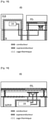
- a first aspect of the invention illustrated in figure 1 and at the picture 2 relates to an integration SI structure intended to be connected to a DS semiconductor device or to a plurality of DS semiconductor devices.
- the integration structure SI comprises a substrate SB, a first face SIS1 and a second face SIS2, the first face SIS1 being intended to receive the semiconductor devices DS, the integration structure SI comprising, at the level of the first face SIS1, preferably arranged in a layer of dielectric material DE, a first 1NR routing level, the first 1NR routing level comprising at least one first conductive routing track PC in a conductive material and at least one first routing track Superconducting PS in a superconducting material.
- each routing track PS, PC whether conductive or superconductive, can also comprise one or more connection zones ZCC, ZCS. Connection balls could, for example, subsequently be deposited at the level of these connection zones ZCC, ZCS.
- the substrate SB is made of silicon or else of epoxy.
- the first SIS1 and second SIS2 faces have a surface comprised between 1 mm 2 and 1600 mm 2 , preferably of square shape.
- the thickness of the substrate SB is between 50 ⁇ m and 1000 ⁇ m.
- the integration SI structure can have several routing levels 1NR, 2NR.
- a second routing level 2NR is present and comprises a second conductive routing track PC2, connected to the first conductive routing track PC by means of an inter-level conductor via VIC as well as a second superconducting routing track PS2, connected to the first superconducting routing track PS by means of a superconducting via VIS inter-levels.
- the conductive routing tracks of different routing levels are interconnected by inter-level conductive vias VIC while the superconducting routing tracks of different routing levels are preferentially interconnected by superconducting vias VIS inter-levels.
- each routing level possibly comprising one or more conductive routing tracks PC and/or one or more superconducting routing tracks PS.
- a routing level may comprise one or more routing tracks of two types (PC conductors and PS superconductors) or else of a single type (PC conductors or PS superconductors). It will also be possible to choose a configuration in which each routing level comprises only one type of routing tracks, the conductive routing tracks PC then being on different routing levels from the superconducting routing tracks PS.
- the first routing level 1NR situated at the level of the first surface SIS1 of the integration structure SI will always include at least one superconducting routing track PS, preferably a plurality of superconducting routing tracks PS.
- an SI integration structure comprises one or more conductive routing tracks PC and/or one or more superconducting routing tracks PS at the level of the first surface of the SI integration structure.
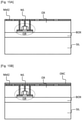
- the latter can also comprise a plurality of through conductor vias VT, the latter passing through the substrate SB so as to connect the second surface SIS2 of the structure integration SI to the conductive track PC or to the conductive tracks PC of the lowest routing level (that is to say the closest to the substrate SB) of the integration SI structure.
- the integration structure SI comprises one or more conductive and/or superconducting inter-level vias VI connecting two successive routing levels.
- the thickness of the barrier layer and/or of the adhesion layer is between 1 nm and 50 nm when the routing track is a superconducting track and limited to a few nanometers (i.e. say less than 10 nm) when the routing track is a conductive routing track so that the material of the barrier layer and/or of the adhesion layer becomes conductive (and no longer superconductive) by proximity effect with the conductive routing track PC2 deposited above. It is useful to note that the order in which the depositions of the barrier layer and of the adhesion layer are made with respect to each other may vary depending on the integration methods used.
- the width of the buried routing tracks is between 0.2 ⁇ m and 500 ⁇ m. In one embodiment, the thickness of the routing tracks is between 50 nm and 5 ⁇ m. Preferably, the routing tracks occupy from 1 to 50% of the first surface SIS1 of the integration structure SI.
- the conductive routing tracks PC2 can in particular be made of copper or tungsten. These materials have the advantage of being compatible with mechanical-chemical polishing processes. More generally, any conductive or superconductive material may be used for the formation of the conductive PC2 or superconductive PS2 routing tracks.
- the superconductive or conductive material is incompatible with a mechanical-chemical polishing method
- one or more conductive PC2 or superconductive PS2 routing tracks are obtained which will then be buried during the manufacture of the inter-level conductive vias VIC, VIS which will now be described.
- a plurality of conductive vias VIC and, optionally, inter-level superconductor VIS VI is obtained, making it possible to connect two successive routing levels to one another.
- Conductor tracks PC of different routing levels can only be connected to each other by means of inter-level conductor vias VIC.
- the superconducting tracks PS of different routing levels are for their part connected to one another by means of conducting vias VIC or, preferably, superconducting vias VIS.
- the thickness of the barrier layer and/or of the adhesion layer is between 1 nm and 50 nm when the routing track is a superconducting track and limited to a few nanometers (i.e. say less than 10 nm) when the routing track is a conductive routing track such that the materials of the barrier layer and/or of the adhesion layer become conductive (and no longer superconductive) by proximity effect with the conductive routing track PC filed above.
- the width of the routing tracks is between 0.2 ⁇ m and 500 ⁇ m. In one embodiment, the thickness of the routing tracks is between 50 nm and 5 ⁇ m. Preferably, the routing tracks occupy from 1 to 50% of the first surface SIS1 of the integration structure SI. It will be noted that the superconducting routing tracks PS, PS2 (buried or not) are never connected to the conducting routing tracks PC or to the through conducting vias VT.
- connection zones ZC in order in particular to protect the latter from oxidation.
- This metallization can for example comprise three layers of different metals, for example titanium, nickel and gold.
- the realization of this metallization can be done by a deposition of the different metal layers, followed by a lithography of the metallization zones, then an etching of the metal layers outside these zones and finally the withdrawal of the resin used during the lithography.
- the thinning step is carried out so as to leave a thickness of substrate SB of between 50 ⁇ m and 300 ⁇ m.
- the density of conductive through-vias VT is between 0.05% and 4% of the surface of the SI integration structure.
- the density of through-conducting vias VT in the transfer zone (i.e. the zone comprising the conductive ZCC and superconductive ZCS connection zones) of the SI integration structure intended to receive the semiconductor devices DS is greater than the density in the other zones of the SI integration structure and at least equal to 1% so as to promote heat exchange between the first face SIS1 and the second face SIS2 of the integration structure.
- the IS integration structure obtained at the end of these steps is illustrated in figure 9 .
- the latter allows routing providing two distinct functions: electrical routing and thermal routing between the various elements (semiconductor devices, interposer, etc.) connected to the SI integration structure.
- the electrical function is ensured by the superconducting routing track(s) PS coupling the various elements connected to the integration structure through one or more routing levels of the integration structure SI.
- the Cooper pairs ensuring the electronic transport in these PS routing tracks do not conduct heat and therefore make it possible to thermally insulate these elements from one another.
- the thermal function is provided by the conductive routing track(s) PC so as to allow the individual thermalization of the various elements connected to the integration structure SI.
- Such “bi-functional” routing is particularly advantageous for the large-scale packaging of spin qubits in silicon.
- the high density of gates necessary for the operation and reading of the qubits is controlled by dedicated CryoCMOS type chips embedded near the qubits to be controlled, for example on the same interposer or on the same SI integration structure.
- the use of a superconducting routing between the qubit chips and the CryoCMOS makes it possible to optimize the electrical signals while suppressing the Joule effect due to these tracks, ensuring one less heat source in the structure, and thermally insulating these chips between them.
- An SI integration structure according to the invention is intended to be mounted in a dilution cryostat.
- the integration structure SI is generally fixed to a printed circuit CI, the mixing box of the cryostat at approximately 10 mK on which the printed circuit is fixed ensuring the cooling of the latter and therefore of the integration structure.
- the integration structure SI is generally fixed to a printed circuit CI, the mixing box of the cryostat at approximately 10 mK on which the printed circuit is fixed ensuring the cooling of the latter and therefore of the integration structure.
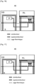
- FIG 10A A first mode of connection of the SI integration structure to the printed circuit is illustrated in figure 10A .
- the integration structure SI is fixed to a printed circuit CI at the level of its second surface SIS2, the conductive routing tracks located on its first surface SIS1 then being connected via connection wires CF, by example using one or more microwelds.
- the thermalization is carried out by the conductive links connecting, via the conductive routing track(s) PC located on the first surface SIS1, the integration structure SI to the printed circuit CI and therefore , indirectly, to the mixing box.
- the connection being made at the level of the first surface SIS1 of the integration structure SI the presence of through vias VT is not necessary.
- FIG. 10B A second mode of connection of the integration structure SI to the printed circuit CI is illustrated in figure 10B .
- the integration structure SI is connected to the printed circuit CI at its second surface SIS2 via conductive balls BI.
- the electrical and thermal coupling is then ensured by the conductive through-vias VT between the second surface SIS2 (and therefore the printed circuit CI) and the routing level closest to the substrate SB at the level of the first surface SIS1 of the structure SI d 'integration.
- the diameter of the conductive balls BI is between 10 ⁇ m and 500 ⁇ m (this diameter being defined by the diameter of the connection zones ZC on which the balls are formed) and the thickness of the conductive balls is between 5 ⁇ m and 500 ⁇ m, the minimum pitch between each conductive ball being equal to 20 ⁇ m.
- the fixing of the integration structure SI to the printed circuit CI is done by means of a mechanical support SM.
- the support comprises a plurality of conductive through vias VI2 making it possible to make the link between each surface of the mechanical support SM.
- the mechanical support SM is fixed to the printed circuit CI via conductive balls BI2 as described previously.
- the integration structure SI is fixed to the mechanical support SM via conductive balls BI, in the same way as described in the previous embodiment.
- the mechanical support SM makes it possible to ensure the mechanical robustness of the integration structure SI in the case where the substrate SB that the latter comprises is thinned.
- this mechanical support SM can constitute the elementary brick of packaging structures of the “bail grid array” or even “land grid array” type.
- the mechanical support SM can allow the splaying of the connections by one or more conductive routing levels associated with the vias VI2 through conductors.
- These packaging structures have the particular advantage of facilitating and accelerating the measurements of devices with a large number of connections.
- An integration structure SI according to the invention is intended to receive one or more semiconductor devices DS.
- a semiconductor device DS intended to be connected to an integration structure SI according to the invention comprises a front face FA and a rear face FR. It generally comprises, at its rear face FR, two types of connection: one or more conductive connections CC and one or more superconductive connections CS. These connections CC, CS are intended to be connected to the connection zones ZCC, ZCS of the routing tracks PC, PS of the same type located on the first surface SIS1 of the integration structure SI.
- the semiconductor device(s) DS are connected to the integration structure SI by means of conductive CBI and superconductive SBI balls. More particularly, at the level of the first surface SIS1 of the SI integration structure, interconnect balls CBI, SBI are made above the routing tracks PC, PS in a material of the same type as the routing track located below the balls (a CBI interconnect ball located above a PC conductive routing track will be a CBI conductive ball; likewise an SBI interconnect ball located above a PS superconducting routing track will be an SBI superconducting ball).
- the semiconductor device DS comprises a front face FA and a rear face FR.
- a plurality of DC, CS connections are located on its rear face FR, some being DC conductive connections and some being DC connections.
- CS superconductors Each superconducting connection CS of the semiconductor device DS is connected by means of a ball SBI in a superconducting material to a superconducting connection zone ZCS located on the first surface SIS1 of the integration structure SI.
- each conductive connection CC of the semiconductor device DS is connected by means of a ball CBI in a conductive material to a conductive connection zone ZCC located on the first surface SIS1 of the integration structure SI.
- the balls of different types are preferably produced on different surfaces of the assembly.
- the conductive balls CBI are made on the rear face FR of the semiconductor device DS while the superconducting balls SBI are made on the first surface SIS1 of the integration structure SI (or vice versa).
- a conductive metallization sub-layer (called UBM for Under-Bump Metallization in English) intended to ensure the connection with the conductive beads located on the rear face of the semiconductor device DS intended to be connected to the SI integration structure, but also a superconducting metallization sub-layer on which the superconducting beads SBI will be formed.
- superconducting balls SBI were formed on the first face SIS1 of the integration structure SI (as illustrated in figure 11 ).
- the superconducting balls have a diameter comprised between 5 ⁇ m and 500 ⁇ m, preferably between 10 ⁇ m and 50 ⁇ m, with a minimum pitch between each ball of 10 ⁇ m.
- a conductive metallization sub-layer, a superconductive metallization sub-layer and conductive balls will be formed on the rear face FR of the semiconductor device DS intended to be connected to the IS integration structure.
- the diameter of the conductive balls CBI is between 10 ⁇ m and 500 ⁇ m, preferably between 10 ⁇ m and 50 ⁇ m, and the latter are spaced apart from each other with a minimum pitch between each ball of 20 ⁇ m.
- the conductive beads CBI and the superconducting beads SBI be dimensioned in the same way in order to guarantee the uniformity of the thickness between the semiconductor device DS and the IS integration structure.
- a filled epoxy-type resin thermally insulating material can be injected between the semiconductor device DS and the integration structure SI to fill the space between these two elements at the level of the interconnect balls and thus further improve the mechanical robustness of the assembly as well as the thermal insulation between the conductive interconnect balls and the superconductive interconnect balls.
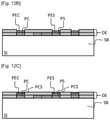
- connection pads PES, PEC are made above the routing tracks PC, PS in a material of the same type as the routing track located in below the pads (a connection pad PEC located above a conductive routing track PC will be made of a conductive material; similarly a connection pad PES located above a superconducting routing track PS will be made in a superconducting material).
- the integration structure SI comprises, on its first surface SIS1, a first plurality of conductive connection pads PEC and a first plurality of superconducting connection pads PES.
- the rear face FR of the semiconductor device DS comprises a second plurality of conductive connection pads CC configured so as to be able to face the first plurality of conductive connection pads PEC and a second plurality of connection pads superconductors CS configured so as to be able to face the first plurality of superconducting connection pads PES, said connection pads being formed in a layer of a dielectric material, for example a passivation layer.
- etching and depositing steps described above are optional, but make it possible to facilitate the mechanical-chemical polishing step which follows, the same material being present on all the connection pads.
- the method then comprises a mechanical-chemical polishing step up to the surface of the layer of a dielectric material.
- a layer of a superconducting material PCS is thus formed on each connection pad PEC, PES.
- the pads thus formed are square in shape (in a parallel plane defined by the first surface SIS1) and have a width of between 0.4 ⁇ m and 25 ⁇ m.
- the surface of the layer of a PCS superconducting material at the end of the CMP step, at the level of the face intended to be bonded to another layer of a PCS superconducting material has a RMS roughness measured on the total surface of a pad less than 0.5 nm. The measurement of this roughness could for example be carried out using an atomic force microscope (or AFM for Atomic Force Microscope in English).
- the thickness of the connection connecting a superconducting routing track of the semiconductor device DS with a superconducting routing track of the integration structure SI is between 600 nm and 1200 nm, preferably equal to 1000 nm (this includes the thickness of the superconducting connection pads on the SI and on the DS as well as the two layers of a superconducting material deposited to ensure bonding and to fuse during annealing). Also, the thickness of the conductive connection (i.e.
- the thickness of the framed structure in the figure 13 will be identical to that of the superconducting connection (that is to say between 600 nm and 1200 nm, preferably equal to 1000 nm), the thickness of the superconducting layer (obtained by melting the superconducting layers during bonding ) being a few nanometers (preferably less than 10 nm).
- the superconducting layer PCS has the main function of ensuring the uniformity of the surfaces during the CMP process preceding bonding.
- the superconducting routing tracks of the structure Integration SI are connected to the superconducting routing tracks of the semiconductor device DS via a stack of superconducting layers.
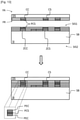
- the conductive routing tracks of the integration structure SI are connected to the conductive routing tracks of the semiconductor device DS by a structure composed of a first layer in a conductive material, a second layer of a superconductive material (corresponding to a first part of the bonding pad), a third layer of a superconductive material (corresponding to a second part of the bonding pad) and a fourth layer of a conductive material (see framed structure on the figure 13 ).
- a heat exchange can take place between the first layer of a conductive material PEC and the fourth layer of a conductive material PEC, and this despite the presence of the two layers of a PCS superconducting material separating them. For this, it is possible to envisage two modes of operation.
- a first mode of operation is based on the proximity effect between the conductive material of the fourth layer of a conductive material PEC and of the first layer of a conductive material PEC, and the superconductive material PCS, this effect making it possible to weaken the superconducting properties of the latter.
- the thickness of superconducting material (that is to say the cumulative thickness of the second layer and of the third superconducting layer) is preferably between 1 and 20 nm.
- a second mode of operation is based on the superconductor/conductor transition when the current which passes through the superconductor material is traversed by a current density greater than a critical current density.
- the thickness of the layer of a superconducting material can be greater than 20 nm: the transition of this metal to its normal mode will take place by applying a current greater than its critical current. For example, if the superconducting material is niobium, knowing that the critical current density is of the order of 10 kA/cm 2 , with a connection pad of 1 ⁇ m of side, a current of the order of 0.1 mA will be sufficient to trigger the superconductor/conductor transition.
- the SI integration structure according to the invention can be particularly advantageous in the context of quantum computing, and in particular for the installation of a "thermal cage" making it possible to isolate the qubits, for example spin qubits, from the heating generally resulting from the operation of the control semiconductor devices in charge of controlling the qubits.
- a DS semiconductor device in charge of controlling a qubit or an array of qubits will be referred to as a PCR control chip and the DS semiconductor device comprising at least one qubit will be referred to as PFL functional chip.
- a control chip PCR may correspond to any heat-generating semiconductor device DS and a functional chip PFL may correspond to any semiconductor device DS which should be isolated from this generated heat.
- the functional chip PFL comprises a substrate P2, preferably made of silicon, comprising a first face and a second face S2, the second face of the substrate P2 forming the front face S2 of the functional chip, said substrate P2 making it possible to to ensure the mechanical robustness of the PFL functional chip. It also comprises a first layer of oxide OXC on the first face of the substrate P2, a second layer of oxide BOX on the first layer of oxide OXC as well as a first level of conductive routing NM1 (i.e.
- the functional chip PFL also comprises a third oxide layer OX on the second oxide layer BOX in which at least one semiconductor component QB is inserted.
- the functional chip comprises a rear face S1 formed by the surface of the third oxide layer opposite the second layer of oxide BOX and capable of being bonded to the first surface SIS1 of an integration structure SI according to the invention, the rear face S1 comprising a second routing level comprising a plurality of superconducting routing tracks NS surrounded at least partially of one or more conductive routing tracks NM2.
- the semiconductor component QB is connected to the superconducting routing tracks NS via superconducting vias VQS so as to be able to electrically control the semiconductor component QB, without however exposing the latter thermally.
- the conductive routing tracks NM2 of the rear face S1 are connected to at least part of the routing tracks of the first level of conductive routing NM1 of the front face S2 by means of conductive vias V12 of so as to form a thermal cage around the semiconductor component, the other routing tracks contributing to the proper thermalization of the rear face S1 and of the front face S2 of the functional chip PFL.
- the QB semiconductor component is a QB qubit, preferably a spin QB qubit formed by a transistor.
- a PFL functional chip according to the invention although it can be connected to structures other than that of the invention, is perfectly suited to the SI integration structure according to the invention insofar as it makes it possible to take advantage of bifunctional routing.
- the conductive level NM1 can be used as a rear biasing gate (or backgate in English).
- the thickness of the second BOX oxide layer is between 10 nm and 1 ⁇ m, preferably between 10 nm and 50 nm.
- the conductive routing tracks NM2 located on the rear face S1 are arranged so as not to face the routing tracks of the first level of conductive routing NM1 located on the surface of the second oxide layer BOX in contact with the first oxide layer OXC. This configuration makes it possible to limit parasitic capacitances.
- the percentage of area of conductive tracks of the first routing level NM1 facing a conductive track NM2 of the second routing level is less than or equal to 10% of the total area of the first routing level NM1, preferably less than or equal to 1% of the total surface of the first routing level NM1.
- the routing tracks NM1 of the front face S2 and the routing tracks NM2 of the rear face S1 are arranged so as to limit the intersections between the routing tracks NM1 of the front face S2 and the NM2 routing of the rear face S1 so as not to form metal loops between the NM1 and NM2 routing levels which could trap a magnetic flux.
- an exclusion zone of a few ⁇ m around the semiconductor component QB could be defined by conditioning the position of the conductive routing tracks NM2 on the first surface S1 and of the conductive routing tracks of the first routing level NM1 conductor.
- the distance between the conductive tracks NM1, NM2 (that is to say the conductive tracks of the first level of conductive routing NM1 and the conductive tracks NM2 of the second level of routing) and the component semiconductor component QB is greater than or equal to 100 ⁇ m to prevent heating of the semiconductor component QB by the conductive routing tracks NM1 and NM2.
- the minimum distance between each routing track NM1, NM2 (that is to say the conductive tracks of the first level of conductive routing NM1 and the conductive tracks NM2 of the second level of routing) is between 1 ⁇ m and 10 ⁇ m, for example equal to 5 ⁇ m, whatever the level of routing considered.
- this minimum distance concerns two routing tracks located on the same routing level or even two routing tracks located on two different routing levels. In the latter case, the distance is measured in the first routing track on the first surface and the projection of the second routing track on the first surface.
- the routing tracks of the first routing level NM1 have a width comprised between 50 nm and 500 ⁇ m, preferably a width equal to 5 ⁇ m.
- the conductive routing tracks NM2 of the second routing level (at the level of the rear face S1) have a width comprised between 50 nm and 10 ⁇ m, preferably a width equal to 1 ⁇ m.
- the conductive vias V12 connecting the conductive routing tracks NM1 of the front face S2 to the conductive routing tracks NM2 of the rear face S1 have a square section. In one embodiment, the width of the square section is between 200 nm and 400 nm. In one embodiment at least some of the vias take the form of a matrix of vias, the vias of said matrix all connecting the same routing tracks. In one embodiment, the matrix of vias is of the form 2 ⁇ 2, that is to say four vias arranged so as to form two columns each comprising two vias. In one embodiment, my via array is 4x4, that is, eight vias arranged to form four columns each comprising four vias. Other shapes are of course possible.
- each superconducting track comprises one or more connection pads (similar to the connection areas described in the case of the integration structure SI) and the various terminals of the semiconductor component QB are each connected to a pad superconducting connection of one of the superconducting routing tracks NS via a superconducting via VQS and the minimum distance I ds between the connection pads connected to the semiconductor component and said semiconductor component is greater than or equal to 5 ⁇ m, preferably greater than or equal to 10 ⁇ m.
- a distance makes it possible to limit the formation of parasitic capacitances between the connection pads and the semiconductor component.
- connection pads of the superconducting routing tracks have a square section with a width comprised between 500 nm and 5 ⁇ m and the superconducting routing tracks NS have a width comprised between 50 nm and 100 ⁇ m.
- each conductive routing track NM2 of the rear face S1 comprises one or more connection pads (similar to the connection areas described in the case of the integration structure SI) and these connection pads have a square section with a width of between 500 nm and 5 ⁇ m These dimensions are particularly advantageous when the PFL chip is intended to be connected to an SI integration structure by bonding.
- some chips can be connected to the SI integration structure by means of conductive and superconductive balls while others can be connected by bonding.
- This AS assembly is shown in figure 18 in which the PCR control chip is connected by conductive and superconductive beads while the PFL functional chip is connected by bonding.
- the SI integration structure and the control chip are simplified while the functional chip has been deformed so as to leave apparent the type of materials used (superconductor or conductor).
- the choice of the hybridization technique (beads or bonding) may in particular depend on the connection densities and therefore on the integration densities of each chip.
- the PCR control chip controls the PFL functional chip by means of one or more superconducting routing tracks, which makes it possible to thermally decouple the PFL functional chip from the PCR control chip.
- the semiconductor component here a qubit
- the thermal cage thermalized by means of the conductive routing tracks of the integration SI structure, so that it finds itself thermally isolated from its close environment and in particular from the PCR control chip.
- a thermal cage is also present around the control circuit CR of the PCR control chip in order to further improve the thermal insulation between the functional chip PFL and the PCR control chip. Although preferable, this thermal cage is however optional for the PCR control chip.
- the SI integration structure is also configured to perform the role of PCR control chip.
- An AS assembly corresponding to this configuration is shown in figure 19 in the particularly advantageous mode where the functional chip is connected by bonding to the integration structure SI configured to operate as a PCR control chip.
- conductive vias at the periphery of the integration structure SI and therefore remote from the control circuit CR, make it possible to thermalize the functional chip PFL so as to be able to form a thermal cage around the latter (shaded area on the figure).
- a thermal half-cage (here it is a half-cage insofar as the cage does not surround the lower part of the control circuit CR) is further formed around the control circuit CR in order to improve the thermal insulation between the latter and the PFL functional chip.
- a resin loaded with thermally insulating epoxy may be injected between the integration structure SI and the semiconductor devices DS connected by means of conductive and superconductive balls.
- This epoxy will improve the mechanical strength of the AS assembly during repeated thermal cycles and thermally insulate the electrical and thermal interconnections.
- the choice of this epoxy must be made to avoid the creation of additional loss mechanisms that could impact the qubits.
- a sixth aspect of the invention illustrated in figure 20 relates to a system SY comprising a printed circuit CI and an assembly AS according to the invention.
- the assembly AS is connected to the printed circuit CI via the integration structure SI by means of conductive balls.
- the assembly AS comprises at least a first semiconductor device DS in the form of a functional chip PFL and a second semiconductor device DS in the form of a control chip PCR.
- the control chip PCR is connected to the functional chip PFL via the integration structure SI by means of superconducting routing tracks PS.
- control chip PCR can electrically control the functional chip PFL without however communicating energy to the latter in the form of heat, the connection being made by means of one or more superconducting routing tracks.
- the PFL functional chip and the PCR control chip are connected to the integration structure by means of one or more conductive routing tracks in order to guarantee good thermalization of the PCR, PFL chips.
- the functional PFL chip is a functional PFL chip according to a fourth aspect of the invention.
- the conductive tracks NM1, NM2 and through-conductor vias V12 of the functional chip PFL come to form a "thermal cage" around the qubit QB, this thermal cage being initiated by the conductive routing tracks and through-conductor vias of the IS integration structure.
- the SY system makes it possible to obtain the cooling diagram illustrated in figure 21 .
- the printed circuit IC is thermalized to a temperature of a few mK by the mixing box of the cryostat.
- the printed circuit CI in turn thermalizes the integration structure SI which, thanks to the bi-functional routing, makes it possible to obtain a thermal cage around the various semiconductor devices PFL, PCR connected to the integration structure SI.
Landscapes
- Engineering & Computer Science (AREA)
- General Physics & Mathematics (AREA)
- Theoretical Computer Science (AREA)
- Physics & Mathematics (AREA)
- Mathematical Analysis (AREA)
- Computing Systems (AREA)
- Evolutionary Computation (AREA)
- Condensed Matter Physics & Semiconductors (AREA)
- Computational Mathematics (AREA)
- Mathematical Optimization (AREA)
- Pure & Applied Mathematics (AREA)
- Data Mining & Analysis (AREA)
- General Engineering & Computer Science (AREA)
- Mathematical Physics (AREA)
- Software Systems (AREA)
- Artificial Intelligence (AREA)
- Superconductor Devices And Manufacturing Methods Thereof (AREA)
- Internal Circuitry In Semiconductor Integrated Circuit Devices (AREA)
- Superconductors And Manufacturing Methods Therefor (AREA)
Applications Claiming Priority (1)
| Application Number | Priority Date | Filing Date | Title |
|---|---|---|---|
| FR2009541A FR3114444B1 (fr) | 2020-09-21 | 2020-09-21 | Puce à routage bifonctionnel et procédé de fabrication associé |
Publications (2)
| Publication Number | Publication Date |
|---|---|
| EP3971982A1 true EP3971982A1 (de) | 2022-03-23 |
| EP3971982B1 EP3971982B1 (de) | 2023-07-26 |
Family
ID=74045640
Family Applications (1)
| Application Number | Title | Priority Date | Filing Date |
|---|---|---|---|
| EP21196606.4A Active EP3971982B1 (de) | 2020-09-21 | 2021-09-14 | Bifunktioneller routing-chip und entsprechendes herstellungsverfahren |
Country Status (4)
| Country | Link |
|---|---|
| US (1) | US11823997B2 (de) |
| EP (1) | EP3971982B1 (de) |
| CN (1) | CN114256357A (de) |
| FR (1) | FR3114444B1 (de) |
Cited By (1)
| Publication number | Priority date | Publication date | Assignee | Title |
|---|---|---|---|---|
| EP4622439A1 (de) | 2024-03-22 | 2025-09-24 | Commissariat à l'Energie Atomique et aux Energies Alternatives | Integrierte kühlstruktur für halbleiter-qubit-quantenvorrichtung |
Families Citing this family (3)
| Publication number | Priority date | Publication date | Assignee | Title |
|---|---|---|---|---|
| JP2024526085A (ja) | 2021-06-11 | 2024-07-17 | シーク, インコーポレイテッド | 超伝導量子回路のための磁束バイアスのシステム及び方法 |
| CN117316920B (zh) * | 2023-09-15 | 2024-08-16 | 江苏卓胜微电子股份有限公司 | 半导体结构及其制备方法 |
| JP2026028554A (ja) * | 2024-08-07 | 2026-02-20 | 富士通株式会社 | デバイスの製造方法及びデバイス |
Citations (5)
| Publication number | Priority date | Publication date | Assignee | Title |
|---|---|---|---|---|
| WO2014168665A2 (en) * | 2013-01-18 | 2014-10-16 | Yale University | Methods for making a superconducting device with at least one enclosure |
| US9530873B1 (en) * | 2013-01-28 | 2016-12-27 | Sandia Corporation | Semiconductor adiabatic qubits |
| WO2018052399A1 (en) | 2016-09-13 | 2018-03-22 | Google Llc | Reducing loss in stacked quantum devices |
| WO2018063204A1 (en) * | 2016-09-29 | 2018-04-05 | Intel Corporation | Quantum computing assemblies |
| US20190273197A1 (en) | 2016-12-27 | 2019-09-05 | Intel Corporation | Superconducting qubit device packages |
Family Cites Families (16)
| Publication number | Priority date | Publication date | Assignee | Title |
|---|---|---|---|---|
| US5061686A (en) * | 1989-05-15 | 1991-10-29 | Hewlett-Packard Company | Superconducting power distribution structure for integrated circuits |
| US8241701B2 (en) * | 2005-08-31 | 2012-08-14 | Lam Research Corporation | Processes and systems for engineering a barrier surface for copper deposition |
| US20070194225A1 (en) * | 2005-10-07 | 2007-08-23 | Zorn Miguel D | Coherent electron junction scanning probe interference microscope, nanomanipulator and spectrometer with assembler and DNA sequencing applications |
| US20080311711A1 (en) * | 2007-06-13 | 2008-12-18 | Roland Hampp | Gapfill for metal contacts |
| US8738105B2 (en) * | 2010-01-15 | 2014-05-27 | D-Wave Systems Inc. | Systems and methods for superconducting integrated circuts |
| US9768371B2 (en) * | 2012-03-08 | 2017-09-19 | D-Wave Systems Inc. | Systems and methods for fabrication of superconducting integrated circuits |
| SG11201505616YA (en) * | 2013-01-18 | 2015-09-29 | Univ Yale | Superconducting device with at least one enclosure |
| US9455391B1 (en) * | 2015-05-19 | 2016-09-27 | The United States Of America As Represented By Secretary Of The Navy | Advanced process flow for quantum memory devices and josephson junctions with heterogeneous integration |
| US9780285B1 (en) * | 2016-08-16 | 2017-10-03 | Northrop Grumman Systems Corporation | Superconductor device interconnect structure |
| US10608159B2 (en) * | 2016-11-15 | 2020-03-31 | Northrop Grumman Systems Corporation | Method of making a superconductor device |
| US20200266234A1 (en) * | 2018-04-20 | 2020-08-20 | D-Wave Systems Inc. | Systems and methods for fabrication of superconducting devices |
| US10546992B2 (en) * | 2018-06-28 | 2020-01-28 | International Business Machines Corporation | Buried electrode geometry for lowering surface losses in superconducting microwave circuits |
| CN112313796B (zh) * | 2018-07-30 | 2023-12-08 | 谷歌有限责任公司 | 载体芯片、制造载体芯片的方法和量子计算器件 |
| US10998486B1 (en) * | 2020-11-10 | 2021-05-04 | Quantala LLC | Reducing qubit energy decay and correlated errors from cosmic rays in quantum processors |
| FR3118961A1 (fr) * | 2021-01-18 | 2022-07-22 | Commissariat A L'energie Atomique Et Aux Energies Alternatives | Dispositif comprenant des grilles de commande électrostatique reparties sur deux faces opposées d’une portion de semi-conducteur |
| FR3126547B1 (fr) * | 2021-08-31 | 2023-08-25 | Commissariat Energie Atomique | Procédé de réalisation d’un siliciure de vanadium supraconducteur sur une couche de silicium |
-
2020
- 2020-09-21 FR FR2009541A patent/FR3114444B1/fr not_active Expired - Fee Related
-
2021
- 2021-09-14 EP EP21196606.4A patent/EP3971982B1/de active Active
- 2021-09-20 US US17/479,472 patent/US11823997B2/en active Active
- 2021-09-22 CN CN202111106121.0A patent/CN114256357A/zh active Pending
Patent Citations (5)
| Publication number | Priority date | Publication date | Assignee | Title |
|---|---|---|---|---|
| WO2014168665A2 (en) * | 2013-01-18 | 2014-10-16 | Yale University | Methods for making a superconducting device with at least one enclosure |
| US9530873B1 (en) * | 2013-01-28 | 2016-12-27 | Sandia Corporation | Semiconductor adiabatic qubits |
| WO2018052399A1 (en) | 2016-09-13 | 2018-03-22 | Google Llc | Reducing loss in stacked quantum devices |
| WO2018063204A1 (en) * | 2016-09-29 | 2018-04-05 | Intel Corporation | Quantum computing assemblies |
| US20190273197A1 (en) | 2016-12-27 | 2019-09-05 | Intel Corporation | Superconducting qubit device packages |
Non-Patent Citations (1)
| Title |
|---|
| ROSENBERG D ET AL: "3D integrated superconducting qubits", ARXIV.ORG, CORNELL UNIVERSITY LIBRARY, 201 OLIN LIBRARY CORNELL UNIVERSITY ITHACA, NY 14853, 13 June 2017 (2017-06-13), XP080769525, DOI: 10.1038/S41534-017-0044-0 * |
Cited By (1)
| Publication number | Priority date | Publication date | Assignee | Title |
|---|---|---|---|---|
| EP4622439A1 (de) | 2024-03-22 | 2025-09-24 | Commissariat à l'Energie Atomique et aux Energies Alternatives | Integrierte kühlstruktur für halbleiter-qubit-quantenvorrichtung |
Also Published As
| Publication number | Publication date |
|---|---|
| FR3114444B1 (fr) | 2022-09-30 |
| CN114256357A (zh) | 2022-03-29 |
| FR3114444A1 (fr) | 2022-03-25 |
| US11823997B2 (en) | 2023-11-21 |
| US20220093501A1 (en) | 2022-03-24 |
| EP3971982B1 (de) | 2023-07-26 |
Similar Documents
| Publication | Publication Date | Title |
|---|---|---|
| EP3971982B1 (de) | Bifunktioneller routing-chip und entsprechendes herstellungsverfahren | |
| EP3971983A1 (de) | Integrationsstruktur mit bifunktionellem routing und anordnung mit einer solchen struktur | |
| AU2018434686B2 (en) | Signal distribution for a quantum computing system | |
| JP2019504511A (ja) | 超伝導バンプボンド | |
| FR3007403A1 (fr) | Procede de realisation d'un dispositif microelectronique mecaniquement autonome | |
| EP3811423B1 (de) | Photonischer chip mit vergrabener laserquelle | |
| EP4120350B1 (de) | Elektronische vorrichtung zum verbinden einer ersten elektronischen komponente mit einer zweiten elektronischen komponente, system mit einer solchen vorrichtung und verfahren zur herstellung einer solchen vorrichtung | |
| Borel et al. | Recent progress in the development of high-density TSV for 3-layers CMOS image sensors | |
| FR3045940A1 (fr) | Dispositif d'inductance et son procede de fabrication | |
| US20250364463A1 (en) | Electronic die assembly comprising bonding pads directly connected to conductive tracks | |
| Motoyoshi et al. | Stacked pixel sensor/detector technology using Au micro-bump junction | |
| Niklaus et al. | Wafer-level 3D integration technology platforms for ICs and MEMS | |
| EP4131421A1 (de) | Vorrichtung zur speicherung, kontrolle und handhabung von quanteninformationen (qubits) auf halbleitern | |
| EP4188061A1 (de) | Integrationsstruktur zur verbindung mehrerer halbleiterbauelemente, verfahren, anordnung und system dafür | |
| FR2994023A1 (fr) | Procede de realisation de vias | |
| US20240162186A1 (en) | Method of fabricating an electronic device | |
| FR3162591A1 (fr) | Assemblage de puces électroniques comprenant des plots d’interconnexion supraconducteurs | |
| EP4572593B1 (de) | Verfahren zur herstellung einer speichervorrichtung und eine speichervorrichtung | |
| EP4709136A1 (de) | Verfahren zur herstellung einer 3d-anordnung | |
| FR3009128A1 (fr) | Procede de realisation d'un plot conducteur sur un element conducteur | |
| TWI517226B (zh) | 形成包含由一共同底材承載之兩個或以上已處理半導體構造之黏附半導體構造之方法及應用此等方法所形成之半導體構造 | |
| FR2964791A1 (fr) | Composant electronique comprenant un via conducteur realisant une fonction de dissipation thermique | |
| EP4199109A1 (de) | Rückgitter für quantenvorrichtung | |
| EP2278613B1 (de) | Röhrenförmige Durchkontaktierung, welche aus mehreren leitfähigen Einzel-Durchkontaktierungen besteht | |
| EP4719027A1 (de) | Verfahren zur herstellung einer hochdichten elektrischen verbindungsstruktur |
Legal Events
| Date | Code | Title | Description |
|---|---|---|---|
| PUAI | Public reference made under article 153(3) epc to a published international application that has entered the european phase |
Free format text: ORIGINAL CODE: 0009012 |
|
| STAA | Information on the status of an ep patent application or granted ep patent |
Free format text: STATUS: REQUEST FOR EXAMINATION WAS MADE |
|
| 17P | Request for examination filed |
Effective date: 20210914 |
|
| AK | Designated contracting states |
Kind code of ref document: A1 Designated state(s): AL AT BE BG CH CY CZ DE DK EE ES FI FR GB GR HR HU IE IS IT LI LT LU LV MC MK MT NL NO PL PT RO RS SE SI SK SM TR |
|
| RBV | Designated contracting states (corrected) |
Designated state(s): AL AT BE BG CH CY CZ DE DK EE ES FI FR GB GR HR HU IE IS IT LI LT LU LV MC MK MT NL NO PL PT RO RS SE SI SK SM TR |
|
| REG | Reference to a national code |
Ref country code: DE Ref legal event code: R079 Free format text: PREVIOUS MAIN CLASS: H01L0027180000 Ipc: H10N0069000000 Ref document number: 602021003770 Country of ref document: DE |
|
| GRAP | Despatch of communication of intention to grant a patent |
Free format text: ORIGINAL CODE: EPIDOSNIGR1 |
|
| STAA | Information on the status of an ep patent application or granted ep patent |
Free format text: STATUS: GRANT OF PATENT IS INTENDED |
|
| RIC1 | Information provided on ipc code assigned before grant |
Ipc: H01L 23/498 20060101ALN20230131BHEP Ipc: H01L 23/44 20060101ALI20230131BHEP Ipc: H10N 60/81 20230101ALI20230131BHEP Ipc: H01L 25/065 20060101ALI20230131BHEP Ipc: H01L 23/532 20060101ALI20230131BHEP Ipc: H01L 29/66 20060101ALI20230131BHEP Ipc: G06N 10/00 20190101ALI20230131BHEP Ipc: B82Y 10/00 20110101ALI20230131BHEP Ipc: H10N 69/00 20230101AFI20230131BHEP |
|
| INTG | Intention to grant announced |
Effective date: 20230220 |
|
| RIN1 | Information on inventor provided before grant (corrected) |
Inventor name: VINET, MAUD Inventor name: COUDRAIN, PERCEVAL Inventor name: CHARBONNIER, JEAN Inventor name: THOMAS, CANDICE |
|
| GRAS | Grant fee paid |
Free format text: ORIGINAL CODE: EPIDOSNIGR3 |
|
| GRAA | (expected) grant |
Free format text: ORIGINAL CODE: 0009210 |
|
| STAA | Information on the status of an ep patent application or granted ep patent |
Free format text: STATUS: THE PATENT HAS BEEN GRANTED |
|
| AK | Designated contracting states |
Kind code of ref document: B1 Designated state(s): AL AT BE BG CH CY CZ DE DK EE ES FI FR GB GR HR HU IE IS IT LI LT LU LV MC MK MT NL NO PL PT RO RS SE SI SK SM TR |
|
| REG | Reference to a national code |
Ref country code: CH Ref legal event code: EP |
|
| REG | Reference to a national code |
Ref country code: IE Ref legal event code: FG4D Free format text: LANGUAGE OF EP DOCUMENT: FRENCH |
|
| REG | Reference to a national code |
Ref country code: DE Ref legal event code: R096 Ref document number: 602021003770 Country of ref document: DE |
|
| REG | Reference to a national code |
Ref country code: LT Ref legal event code: MG9D |
|
| REG | Reference to a national code |
Ref country code: NL Ref legal event code: MP Effective date: 20230726 |
|
| REG | Reference to a national code |
Ref country code: AT Ref legal event code: MK05 Ref document number: 1593501 Country of ref document: AT Kind code of ref document: T Effective date: 20230726 |
|
| PG25 | Lapsed in a contracting state [announced via postgrant information from national office to epo] |
Ref country code: NL Free format text: LAPSE BECAUSE OF FAILURE TO SUBMIT A TRANSLATION OF THE DESCRIPTION OR TO PAY THE FEE WITHIN THE PRESCRIBED TIME-LIMIT Effective date: 20230726 |
|
| PG25 | Lapsed in a contracting state [announced via postgrant information from national office to epo] |
Ref country code: GR Free format text: LAPSE BECAUSE OF FAILURE TO SUBMIT A TRANSLATION OF THE DESCRIPTION OR TO PAY THE FEE WITHIN THE PRESCRIBED TIME-LIMIT Effective date: 20231027 |
|
| PG25 | Lapsed in a contracting state [announced via postgrant information from national office to epo] |
Ref country code: IS Free format text: LAPSE BECAUSE OF FAILURE TO SUBMIT A TRANSLATION OF THE DESCRIPTION OR TO PAY THE FEE WITHIN THE PRESCRIBED TIME-LIMIT Effective date: 20231126 |
|
| PG25 | Lapsed in a contracting state [announced via postgrant information from national office to epo] |
Ref country code: SE Free format text: LAPSE BECAUSE OF FAILURE TO SUBMIT A TRANSLATION OF THE DESCRIPTION OR TO PAY THE FEE WITHIN THE PRESCRIBED TIME-LIMIT Effective date: 20230726 Ref country code: RS Free format text: LAPSE BECAUSE OF FAILURE TO SUBMIT A TRANSLATION OF THE DESCRIPTION OR TO PAY THE FEE WITHIN THE PRESCRIBED TIME-LIMIT Effective date: 20230726 Ref country code: PT Free format text: LAPSE BECAUSE OF FAILURE TO SUBMIT A TRANSLATION OF THE DESCRIPTION OR TO PAY THE FEE WITHIN THE PRESCRIBED TIME-LIMIT Effective date: 20231127 Ref country code: NO Free format text: LAPSE BECAUSE OF FAILURE TO SUBMIT A TRANSLATION OF THE DESCRIPTION OR TO PAY THE FEE WITHIN THE PRESCRIBED TIME-LIMIT Effective date: 20231026 Ref country code: LV Free format text: LAPSE BECAUSE OF FAILURE TO SUBMIT A TRANSLATION OF THE DESCRIPTION OR TO PAY THE FEE WITHIN THE PRESCRIBED TIME-LIMIT Effective date: 20230726 Ref country code: LT Free format text: LAPSE BECAUSE OF FAILURE TO SUBMIT A TRANSLATION OF THE DESCRIPTION OR TO PAY THE FEE WITHIN THE PRESCRIBED TIME-LIMIT Effective date: 20230726 Ref country code: IS Free format text: LAPSE BECAUSE OF FAILURE TO SUBMIT A TRANSLATION OF THE DESCRIPTION OR TO PAY THE FEE WITHIN THE PRESCRIBED TIME-LIMIT Effective date: 20231126 Ref country code: HR Free format text: LAPSE BECAUSE OF FAILURE TO SUBMIT A TRANSLATION OF THE DESCRIPTION OR TO PAY THE FEE WITHIN THE PRESCRIBED TIME-LIMIT Effective date: 20230726 Ref country code: GR Free format text: LAPSE BECAUSE OF FAILURE TO SUBMIT A TRANSLATION OF THE DESCRIPTION OR TO PAY THE FEE WITHIN THE PRESCRIBED TIME-LIMIT Effective date: 20231027 Ref country code: FI Free format text: LAPSE BECAUSE OF FAILURE TO SUBMIT A TRANSLATION OF THE DESCRIPTION OR TO PAY THE FEE WITHIN THE PRESCRIBED TIME-LIMIT Effective date: 20230726 Ref country code: AT Free format text: LAPSE BECAUSE OF FAILURE TO SUBMIT A TRANSLATION OF THE DESCRIPTION OR TO PAY THE FEE WITHIN THE PRESCRIBED TIME-LIMIT Effective date: 20230726 |
|
| PG25 | Lapsed in a contracting state [announced via postgrant information from national office to epo] |
Ref country code: PL Free format text: LAPSE BECAUSE OF FAILURE TO SUBMIT A TRANSLATION OF THE DESCRIPTION OR TO PAY THE FEE WITHIN THE PRESCRIBED TIME-LIMIT Effective date: 20230726 |
|
| PG25 | Lapsed in a contracting state [announced via postgrant information from national office to epo] |
Ref country code: ES Free format text: LAPSE BECAUSE OF FAILURE TO SUBMIT A TRANSLATION OF THE DESCRIPTION OR TO PAY THE FEE WITHIN THE PRESCRIBED TIME-LIMIT Effective date: 20230726 |
|
| REG | Reference to a national code |
Ref country code: DE Ref legal event code: R097 Ref document number: 602021003770 Country of ref document: DE |
|
| PG25 | Lapsed in a contracting state [announced via postgrant information from national office to epo] |
Ref country code: SM Free format text: LAPSE BECAUSE OF FAILURE TO SUBMIT A TRANSLATION OF THE DESCRIPTION OR TO PAY THE FEE WITHIN THE PRESCRIBED TIME-LIMIT Effective date: 20230726 Ref country code: RO Free format text: LAPSE BECAUSE OF FAILURE TO SUBMIT A TRANSLATION OF THE DESCRIPTION OR TO PAY THE FEE WITHIN THE PRESCRIBED TIME-LIMIT Effective date: 20230726 Ref country code: ES Free format text: LAPSE BECAUSE OF FAILURE TO SUBMIT A TRANSLATION OF THE DESCRIPTION OR TO PAY THE FEE WITHIN THE PRESCRIBED TIME-LIMIT Effective date: 20230726 Ref country code: EE Free format text: LAPSE BECAUSE OF FAILURE TO SUBMIT A TRANSLATION OF THE DESCRIPTION OR TO PAY THE FEE WITHIN THE PRESCRIBED TIME-LIMIT Effective date: 20230726 Ref country code: DK Free format text: LAPSE BECAUSE OF FAILURE TO SUBMIT A TRANSLATION OF THE DESCRIPTION OR TO PAY THE FEE WITHIN THE PRESCRIBED TIME-LIMIT Effective date: 20230726 Ref country code: CZ Free format text: LAPSE BECAUSE OF FAILURE TO SUBMIT A TRANSLATION OF THE DESCRIPTION OR TO PAY THE FEE WITHIN THE PRESCRIBED TIME-LIMIT Effective date: 20230726 Ref country code: SK Free format text: LAPSE BECAUSE OF FAILURE TO SUBMIT A TRANSLATION OF THE DESCRIPTION OR TO PAY THE FEE WITHIN THE PRESCRIBED TIME-LIMIT Effective date: 20230726 |
|
| PG25 | Lapsed in a contracting state [announced via postgrant information from national office to epo] |
Ref country code: LU Free format text: LAPSE BECAUSE OF NON-PAYMENT OF DUE FEES Effective date: 20230914 |
|
| REG | Reference to a national code |
Ref country code: BE Ref legal event code: MM Effective date: 20230930 |
|
| PG25 | Lapsed in a contracting state [announced via postgrant information from national office to epo] |
Ref country code: LU Free format text: LAPSE BECAUSE OF NON-PAYMENT OF DUE FEES Effective date: 20230914 Ref country code: IT Free format text: LAPSE BECAUSE OF FAILURE TO SUBMIT A TRANSLATION OF THE DESCRIPTION OR TO PAY THE FEE WITHIN THE PRESCRIBED TIME-LIMIT Effective date: 20230726 Ref country code: MC Free format text: LAPSE BECAUSE OF FAILURE TO SUBMIT A TRANSLATION OF THE DESCRIPTION OR TO PAY THE FEE WITHIN THE PRESCRIBED TIME-LIMIT Effective date: 20230726 |
|
| PLBE | No opposition filed within time limit |
Free format text: ORIGINAL CODE: 0009261 |
|
| STAA | Information on the status of an ep patent application or granted ep patent |
Free format text: STATUS: NO OPPOSITION FILED WITHIN TIME LIMIT |
|
| 26N | No opposition filed |
Effective date: 20240429 |
|
| REG | Reference to a national code |
Ref country code: IE Ref legal event code: MM4A |
|
| PG25 | Lapsed in a contracting state [announced via postgrant information from national office to epo] |
Ref country code: IE Free format text: LAPSE BECAUSE OF NON-PAYMENT OF DUE FEES Effective date: 20230914 |
|
| PG25 | Lapsed in a contracting state [announced via postgrant information from national office to epo] |
Ref country code: IE Free format text: LAPSE BECAUSE OF NON-PAYMENT OF DUE FEES Effective date: 20230914 Ref country code: SI Free format text: LAPSE BECAUSE OF FAILURE TO SUBMIT A TRANSLATION OF THE DESCRIPTION OR TO PAY THE FEE WITHIN THE PRESCRIBED TIME-LIMIT Effective date: 20230726 |
|
| PG25 | Lapsed in a contracting state [announced via postgrant information from national office to epo] |
Ref country code: BE Free format text: LAPSE BECAUSE OF NON-PAYMENT OF DUE FEES Effective date: 20230930 |
|
| PG25 | Lapsed in a contracting state [announced via postgrant information from national office to epo] |
Ref country code: BG Free format text: LAPSE BECAUSE OF FAILURE TO SUBMIT A TRANSLATION OF THE DESCRIPTION OR TO PAY THE FEE WITHIN THE PRESCRIBED TIME-LIMIT Effective date: 20230726 |
|
| PG25 | Lapsed in a contracting state [announced via postgrant information from national office to epo] |
Ref country code: BG Free format text: LAPSE BECAUSE OF FAILURE TO SUBMIT A TRANSLATION OF THE DESCRIPTION OR TO PAY THE FEE WITHIN THE PRESCRIBED TIME-LIMIT Effective date: 20230726 |
|
| REG | Reference to a national code |
Ref country code: CH Ref legal event code: PL |
|
| PG25 | Lapsed in a contracting state [announced via postgrant information from national office to epo] |
Ref country code: CH Free format text: LAPSE BECAUSE OF NON-PAYMENT OF DUE FEES Effective date: 20240930 |
|
| PG25 | Lapsed in a contracting state [announced via postgrant information from national office to epo] |
Ref country code: CY Free format text: LAPSE BECAUSE OF FAILURE TO SUBMIT A TRANSLATION OF THE DESCRIPTION OR TO PAY THE FEE WITHIN THE PRESCRIBED TIME-LIMIT; INVALID AB INITIO Effective date: 20210914 |
|
| PG25 | Lapsed in a contracting state [announced via postgrant information from national office to epo] |
Ref country code: HU Free format text: LAPSE BECAUSE OF FAILURE TO SUBMIT A TRANSLATION OF THE DESCRIPTION OR TO PAY THE FEE WITHIN THE PRESCRIBED TIME-LIMIT; INVALID AB INITIO Effective date: 20210914 |
|
| PGFP | Annual fee paid to national office [announced via postgrant information from national office to epo] |
Ref country code: DE Payment date: 20250919 Year of fee payment: 5 |
|
| PGFP | Annual fee paid to national office [announced via postgrant information from national office to epo] |
Ref country code: GB Payment date: 20250923 Year of fee payment: 5 |
|
| PGFP | Annual fee paid to national office [announced via postgrant information from national office to epo] |
Ref country code: FR Payment date: 20250923 Year of fee payment: 5 |
|
| PG25 | Lapsed in a contracting state [announced via postgrant information from national office to epo] |
Ref country code: TR Free format text: LAPSE BECAUSE OF FAILURE TO SUBMIT A TRANSLATION OF THE DESCRIPTION OR TO PAY THE FEE WITHIN THE PRESCRIBED TIME-LIMIT Effective date: 20230726 |