EP3970324B1 - Dispositif émetteur/récepteur et dispositif de commande de communication pour une station d'abonné d'un système de bus série et procédé de communication dans un système de bus série - Google Patents
Dispositif émetteur/récepteur et dispositif de commande de communication pour une station d'abonné d'un système de bus série et procédé de communication dans un système de bus série Download PDFInfo
- Publication number
- EP3970324B1 EP3970324B1 EP20724076.3A EP20724076A EP3970324B1 EP 3970324 B1 EP3970324 B1 EP 3970324B1 EP 20724076 A EP20724076 A EP 20724076A EP 3970324 B1 EP3970324 B1 EP 3970324B1
- Authority
- EP
- European Patent Office
- Prior art keywords
- communication control
- operating mode
- signal
- communication
- control device
- Prior art date
- Legal status (The legal status is an assumption and is not a legal conclusion. Google has not performed a legal analysis and makes no representation as to the accuracy of the status listed.)
- Active
Links
- 238000004891 communication Methods 0.000 title claims description 213
- 238000000034 method Methods 0.000 title claims description 21
- 230000005540 biological transmission Effects 0.000 claims description 57
- 238000011156 evaluation Methods 0.000 claims description 7
- 230000008901 benefit Effects 0.000 description 6
- 238000010586 diagram Methods 0.000 description 5
- 101100172132 Mus musculus Eif3a gene Proteins 0.000 description 4
- 238000012986 modification Methods 0.000 description 3
- 230000004048 modification Effects 0.000 description 3
- 230000011664 signaling Effects 0.000 description 3
- 230000007704 transition Effects 0.000 description 3
- 230000015572 biosynthetic process Effects 0.000 description 2
- 230000000717 retained effect Effects 0.000 description 2
- 230000000630 rising effect Effects 0.000 description 2
- 238000007792 addition Methods 0.000 description 1
- 230000008859 change Effects 0.000 description 1
- 230000008878 coupling Effects 0.000 description 1
- 238000010168 coupling process Methods 0.000 description 1
- 238000005859 coupling reaction Methods 0.000 description 1
- 230000001419 dependent effect Effects 0.000 description 1
- 238000013461 design Methods 0.000 description 1
- 238000011161 development Methods 0.000 description 1
- 230000010354 integration Effects 0.000 description 1
- 230000008569 process Effects 0.000 description 1
- 238000011084 recovery Methods 0.000 description 1
- 230000009467 reduction Effects 0.000 description 1
- 230000008054 signal transmission Effects 0.000 description 1
Images


Classifications
-
- H—ELECTRICITY
- H04—ELECTRIC COMMUNICATION TECHNIQUE
- H04L—TRANSMISSION OF DIGITAL INFORMATION, e.g. TELEGRAPHIC COMMUNICATION
- H04L12/00—Data switching networks
- H04L12/28—Data switching networks characterised by path configuration, e.g. LAN [Local Area Networks] or WAN [Wide Area Networks]
- H04L12/40—Bus networks
- H04L12/40169—Flexible bus arrangements
-
- H—ELECTRICITY
- H04—ELECTRIC COMMUNICATION TECHNIQUE
- H04L—TRANSMISSION OF DIGITAL INFORMATION, e.g. TELEGRAPHIC COMMUNICATION
- H04L12/00—Data switching networks
- H04L12/28—Data switching networks characterised by path configuration, e.g. LAN [Local Area Networks] or WAN [Wide Area Networks]
- H04L12/40—Bus networks
- H04L12/40006—Architecture of a communication node
- H04L12/40032—Details regarding a bus interface enhancer
-
- H—ELECTRICITY
- H04—ELECTRIC COMMUNICATION TECHNIQUE
- H04L—TRANSMISSION OF DIGITAL INFORMATION, e.g. TELEGRAPHIC COMMUNICATION
- H04L12/00—Data switching networks
- H04L12/28—Data switching networks characterised by path configuration, e.g. LAN [Local Area Networks] or WAN [Wide Area Networks]
- H04L12/40—Bus networks
- H04L12/4013—Management of data rate on the bus
-
- H—ELECTRICITY
- H04—ELECTRIC COMMUNICATION TECHNIQUE
- H04L—TRANSMISSION OF DIGITAL INFORMATION, e.g. TELEGRAPHIC COMMUNICATION
- H04L12/00—Data switching networks
- H04L12/28—Data switching networks characterised by path configuration, e.g. LAN [Local Area Networks] or WAN [Wide Area Networks]
- H04L12/40—Bus networks
- H04L2012/40208—Bus networks characterized by the use of a particular bus standard
- H04L2012/40215—Controller Area Network CAN
Definitions
- the present invention relates to a transmitting/receiving device and a communication control device for a subscriber station of a serial bus system and a method for communication in a serial bus system that operates with a high data rate and is highly error-resistant.
- a bus system is often used for communication between sensors and control devices, for example in vehicles, in which data is transmitted as messages in the ISO11898-1:2015 standard as a CAN protocol specification with CAN FD.
- the messages are transmitted between the bus users of the bus system, such as sensors, control units, encoders, etc.
- CAN FD In order to be able to transmit data with a higher bit rate than with CAN, an option for switching to a higher bit rate within a message was created in the CAN FD message format. With such techniques, the maximum possible data rate is increased beyond a value of 1 Mbit/s by using higher clocking in the area of the data fields.
- Such messages are also referred to below as CAN FD frames or CAN FD messages.
- CAN FD With CAN FD, the user data length has been extended from 8 to 64 bytes and the data transmission rates are significantly higher than with CAN.
- CAN or CAN FD-based communication network offers many advantages in terms of its robustness, for example, it is significantly slower than data transmission with 100 Base-T1 Ethernet, for example.
- the user data length of up to 64 bytes achieved with CAN FD is too small for some applications.
- a CAN FD successor bus system should at least meet such requirements.
- EP 2 940 935 A1 discloses an apparatus and method for controlling CAN bus communications.
- US 2016/0344552 A1 refers to a configurable encryption device for CAN.
- US 2014/0365693 A1 shows a device and a method for a CAN bus, via which CAN FD-capable and non-CAN FD-capable subscriber stations communicate. None of these documents show a mode switching block as described in the following description and claims.
- a transmitting/receiving device and a communication control device for a subscriber station of a serial bus system and a method for communication in a serial bus system are to be provided, in which a high data rate and an increase in the amount of user data per frame can be realized with high error robustness.
- the transmitting/receiving device has a first connection for receiving a transmission signal from a communication control device, a transmitter for transmitting the transmission signal to a bus of the bus system, in which bus system at least a first communication phase and a second communication phase are used to exchange messages between subscriber stations of the bus system , a receiver for receiving the signal from the bus, wherein the receiver is designed to generate a digital received signal from the signal received from the bus, a second connection for sending the digital received signal to the communication control device and for receiving an additional signal from the communication control device, and an operating mode switching block for evaluating the signal from the receiver output received signal and a signal received at the second connection by the communication control device, wherein the operating mode switching block is designed to switch the transmitter and/or the receiver to one of at least two different operating modes depending on a result of the evaluation and at least one predetermined operating mode of the To switch operating modes to another of the operating modes after a
- the transmission/reception device With the transmission/reception device, it is possible, in particular, for communication to take place between the communication control device and the transmission/reception device, particularly when switching between a first communication phase and a second communication phase, without the need for additional, expensive connections between the communication control device and the transmission / receiving equipment would be necessary. Depending on requirements, only one-way communication is possible. Alternatively, however, communication can first take place, for example from the communication control device to the transceiver and then from the transceiver to the communication control device.
- an arbitration known from CAN can be retained with the transceiver in one of the communication phases and the transmission rate can still be increased considerably compared to CAN or CAN FD.
- This can be achieved in that two communication phases with different bit rates are used and the beginning of the second communication phase, in which the user data is transmitted with a higher bit rate than in the arbitration, is reliably identified for the transceiver. Therefore, the transceiver can safely move from a first communication phase to the second communication phase switch.
- the bit rate and thus the transmission speed from the transmitter to the receiver can be increased significantly.
- a high level of error robustness is guaranteed. This helps to achieve a net data rate of at least 10 Mbps.
- the size of the user data can be greater than 64 bytes, in particular up to 4096 bytes per frame, or have any length as required.
- the method carried out by the transmitting/receiving device can also be used if there is also at least one CAN subscriber station and/or at least one CAN FD subscriber station in the bus system, which send messages according to the CAN protocol and/or CAN FD protocol .
- the operating mode switching block is designed to switch the transmitter and/or the receiver to one of at least three different operating modes depending on a result of the evaluation and to switch at least one predetermined operating mode of the three operating modes to one after a period of time preset in the operating mode switching block has expired switch other of the at least three operating modes.
- the at least one predetermined operating mode is the internal communication between the communication control device and the transceiver via the second connection.
- the operating mode switching block can be designed to switch off the transmitter in the at least one predetermined operating mode.
- the transmitter may be configured to drive bits of the signals onto the bus in the first communication phase with a first bit time that is at least a factor of 10 greater than a second bit time of bits that the transmitter drives onto the bus in the second communication phase.
- the signals via the first and second connection in the predetermined operating mode can have bits with a third bit time that is smaller than the second bit time.
- the aforementioned task is also performed by a communication control device for a subscriber station of a serial Bus system with the features of claim 8 solved.
- the communication control device has a communication control module for generating a transmission signal for controlling communication between the subscriber station and at least one other subscriber station in the bus system, in which bus system at least a first communication phase and a second communication phase are used to exchange messages between subscriber stations in the bus system, a first connection for sending of the transmission signal to a transmission/reception device, which is designed to transmit the transmission signal to a bus of the bus system, a second connection for receiving a digital reception signal from the transmission/reception device, wherein the communication control device is designed to generate an additional signal, which the Transmitting/receiving device indicates that the current operating mode must be switched to another operating mode from at least two different operating modes, and which, in addition, internal communication between the communication control module for a period of time that can be preset in the communication control module and an operating mode switching block of the transmitting/receiving device and the trans
- the communication control device offers the same advantages as those mentioned above in relation to the transceiver.
- the preset time period can be divided into a first time period in which the second connection is operated, in particular by the operating mode switching block, in such a way that the communication control device can send data via the second connection, and a second time period in which the communication control device can send data via the second connection receives data, the data sent in the preset period of time being data that is additional information about the signals that are generated in the bus system for the exchange of messages between subscriber stations of the bus system.
- the at least one predetermined operating mode has an operating mode in which the communication control device is configured to send a clock signal via the first connection and in time with the clock signal via the second connection to send data at least temporarily and to receive data at least temporarily, and/or has an operating mode in which the communication control device is configured to use Manchester coding for the data for data exchange with the transceiver.
- the at least one predetermined operating mode it is also conceivable for the at least one predetermined operating mode to have an operating mode in which the transceiver does not drive a transmission signal onto the bus.
- the communication control device can be configured to send an identifier with a predetermined value to the receiver at the connection for the digital reception signal when sending protocol information at the connection for the transmission signal, which signals a switchover from the at least one first communication phase to the second communication phase .
- the identifier is a bit with a predetermined value or pulse pattern, or the identifier is a predetermined bit pattern.
- the signal received from the bus in the first communication phase is generated with a different physical layer than the signal received from the bus (40) in the second communication phase.
- the transceiver in the first communication phase it is negotiated which of the subscriber stations of the bus system is given at least temporarily exclusive, collision-free access to the bus in the subsequent second communication phase.
- the transmitting/receiving device described above and the communication control device described above can be part of a subscriber station of a bus system which also includes a bus and at least two subscriber stations which are connected to one another via the bus in such a way that they can communicate with one another serially.
- at least one of the at least two subscriber stations has a transmitting/receiving device as described above and a communication control device as described above.
- the aforementioned object is also achieved by a method for communication in a serial bus system according to claim 15.
- the method is carried out with a subscriber station for a bus system in which at least a first communication phase and a second communication phase are used to exchange messages between subscriber stations of the bus system, the subscriber station having a transmitter, a receiver, an operating mode switching block, a first connection and has a second connection, and wherein the method has the steps of receiving, with the receiver, a signal from the bus of the bus system, generating, with the receiver, a digital reception signal from the signal received from the bus and outputting the digital reception signal at the second connection, evaluating, with the operating mode switching block, the received signal output by the receiver and a signal received at the second connection from the communication control device, and switching, with the operating mode switching block, the transmitter and/or the receiver depending on a result of the Evaluation in one of at least two different operating modes and switching from at least one predetermined operating mode of the operating modes after a period of time that is preset in the operating mode switching block
- the method offers the same advantages as mentioned above in relation to the transceiver and/or the communication control device.
- bus system 1 shows an example of a bus system 1, which is designed in particular fundamentally for a CAN bus system, a CAN FD bus system, a CAN FD successor bus system, and/or modifications thereof, as described below.
- the bus system 1 can be used in a vehicle, in particular a motor vehicle, an airplane, etc., or in a hospital, etc.
- the bus system 1 has a large number of subscriber stations 10, 20, 30, which are each connected to a bus 40 with a first bus wire 41 and a second bus wire 42.
- the bus cores 41, 42 can also be called CAN_H and CAN_L and are used for electrical signal transmission after coupling in the dominant level or generation of recessive levels for a signal in the transmission state.
- Messages 45, 46 in the form of signals can be transmitted serially between the individual subscriber stations 10, 20, 30 via the bus 40.
- the subscriber stations 10, 20, 30 are, for example, control units, sensors, display devices, etc. of a motor vehicle.
- the subscriber station 10 has a communication control device 11, a transceiver 12 and a switching block 15.
- the subscriber station 20, however, has a communication control device 21 and a transceiver 22.
- the subscriber station 30 has a communication control device 31, a Transmitting / receiving device 32 and a switching block 35.
- the transmitting / receiving devices 12, 22, 32 of the subscriber stations 10, 20, 30 are each connected directly to the bus 40, even if this is in 1 is not illustrated.
- the messages 45, 46 are encoded bit by bit in the form of frames via a TXD line and an RXD line between the respective communication control device 11, 21, 31 and the associated transceiver devices 12, 22, 32 exchanged. This is described in more detail below.
- the communication control devices 11, 21, 31 are each used to control communication between the respective subscriber station 10, 20, 30 via the bus 40 and at least one other subscriber station of the subscriber stations 10, 20, 30 that are connected to the bus 40.
- the communication control devices 11, 31 create and read first messages 45, which are, for example, modified CAN messages 45, which are also called CAN XL messages 45 below.
- the modified CAN messages 45 or CAN XL messages 45 are constructed on the basis of a CAN FD successor format that is related to 2 is described in more detail.
- the communication control devices 11, 31 can also be designed to provide or receive a CAN XL message 45 or a CAN FD message 46 for the transceiver devices 12, 32 as required.
- the communication control devices 11, 31 thus create and read a first message 45 or a second message 46, with the first and second message 45, 46 differing in their data transmission standard, namely CAN XL or CAN FD in this case.
- the communication control device 21 can be designed like a conventional CAN controller according to ISO 11898-1:2015, in particular like a CAN FD tolerant classic CAN controller or a CAN FD controller.
- the communication control device 21 creates and reads second messages 46, for example classic CAN messages or CAN FD messages 46.
- the CAN FD messages 46 can include a number of 0 to 64 data bytes, which also have a significantly faster data rate than with one Classical CAN message to be transmitted. In the latter case, the communication control device 21 is designed like a conventional CAN FD controller.
- the transmitting/receiving devices 12, 32 can be designed as CAN XL transceivers, apart from the differences described in more detail below.
- the transceivers 12, 32 can additionally or alternatively be designed like a conventional CAN FD transceiver.
- the transceiver 22 can be designed like a conventional CAN transceiver or CAN FD transceiver.
- the CAN XL frame 450 is divided into different communication phases 451 to 454 for the CAN communication on the bus 40, namely an arbitration phase 451, a switching phase 452, which is at the end of the arbitration phase, a data phase 453 and a frame end phase 454.
- a bit is sent at the beginning, which is also called the SOF bit and indicates the beginning of the frame or start of frame.
- an identifier with, for example, 11 bits for identifying the sender of the message 45 is also sent.
- the identifier is used to negotiate bit by bit between the subscriber stations 10, 20, 30 which subscriber station 10, 20, 30 would like to send the message 45, 46 with the highest priority and therefore for the next time to send in the switching phase 452 and the subsequent data phase 453 gets exclusive access to the bus 40 of the bus system 1.
- the switching from the arbitration phase 451 to the data phase 453 is prepared in the present exemplary embodiment, with protocol format information contained in at least one bit being sent, which is suitable for CAN XL frames compared to CAN frames or CAN FD frames.
- a 12-bit data length code (data length code), for example, can be sent, which can then, for example, assume values from 1 to 4096, in particular up to 2048 or another value with an increment of 1, or alternatively values of 0 up to 4095 or higher.
- the data length code can also include fewer or more bits and the value range and the increment can assume other values.
- the user data of the CAN XL frame 450 or of the message 45 is sent, which can also be referred to as the data field of the message 45.
- the user data can have, for example, up to 4096 bytes or a larger value or any other value.
- a checksum field can contain a checksum over the data of the data phase 453 including the stuff bits, which the sender of the message 45 inserts as an inverse bit after a predetermined number of identical bits, in particular 10 identical bits.
- at least one acknowledge bit can be contained in an end field in the frame end phase 454 . There may also be a sequence of 11 equal bits indicating the end of the CAN XL frame 450. The at least one acknowledgment bit can be used to communicate whether a receiver has discovered an error in the received CAN XL frame 450 or the message 45 or not.
- a physical layer is used as in CAN and CAN-FD.
- a physical layer as in the case of CAN and CAN-FD can be used at least partially, ie at the beginning, in the switchover phase 452 .
- the physical layer corresponds to the physical layer or layer 1 of the well-known OSI model (Open Systems Interconnection model).
- the arbitration at the beginning of a frame 450 or the message 45, 46 and the acknowledgment in the frame end phase 454 of the frame 450 or the message 45, 46 is only possible if the bit time is significantly more than twice as long as the signal Running time between any two subscriber stations 10, 20, 30 of the bus system 1. Therefore, the bit rate in the arbitration phase 451, the frame end phase 454 and at least partially in the switching phase 452 is selected to be slower than in the data phase 453 of the frame 450.
- the bit rate in the Phases 451, 452, 454 are chosen as 500 kbit/s, from which a bit time of approx.
- bit time of the signal in the other communication phases 451, 452, 454 is at least a factor of 10 greater than the bit time of the signal in the data phase 453.
- a sender of the message 45 for example the subscriber station 10, does not start sending bits of the switching phase 452 and the subsequent data phase 453 to the bus 40 until the subscriber station 10 as the sender has won the arbitration and the subscriber station 10 as the sender has thus started to transmit has exclusive access to the bus 40 of the bus system 1.
- the transmitter can either switch to the faster bit rate and/or the other physical layer after part of the switching phase 452 or only switch to the faster bit rate and/or the other physical layer with the first bit, i.e. at the beginning of the subsequent data phase 453 .
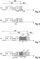
- FIG 3 shows the basic structure of the subscriber station 10 with the communication control device 11, the transceiver 12 and the switching block 15.
- the subscriber station 30 is constructed in a similar way as in FIG 3 shown, except that the block 35 is not integrated into the communication controller 31 but is provided separately from the communication controller 31 and the transceiver 32 . Therefore, the subscriber station 30 and the block 35 will not be described separately.
- the functions of the switchover block 15 described below are identical in the switchover block 35 .
- ASIC application-specific integrated circuit
- the transceiver 12 and an energy supply device can be installed in the system ASIC, which supplies the transceiver 12 with electrical energy.
- the energy supply device usually delivers a voltage CAN_Supply of 5 V. Depending on requirements, however, the energy supply device can deliver a different voltage with a different value and/or be designed as a current source.
- the transceiver 12 also has a transmitter 121 , a receiver 122 , a driver 123 for the transmission signal, a reception signal output driver 124 and a driver 125 which outputs a signal RxD_TC to the switching block 15 .
- the switching block 15 uses the signal RxD_TC and a signal S_SW, which is the output signal of the receiver 122, to form an operating state switching signal S_OP for switching the transmitter 121 and/or the receiver 122.
- the switching signal S_OP can, for example, contain the switching signal for transmitters in one bit 121 and receiver 122 included.
- the switching signal S_OP can be a two-bit signal in order to control the transmitter 121 and receiver 122 separately, for example by providing the first bit to switch the transmitter 121 and the second bit to switch the receiver 122 .
- the transmitter 121 is also referred to as a transmitter.
- the receiver 122 is also referred to as a receiver.
- the switchover block 15 can be configured as a switching block, which in particular has at least one flip-flop. This is below in relation to Figures 4 to 8 described in more detail.
- the transmitter/receiver device 12 is always referred to below, it is alternatively possible to provide the receiver 122 in a separate device external to the transmitter 121 .
- the transmitter 121 and the receiver 122 can be constructed as in a conventional transceiver 22 .
- the transmitter 121 can have at least one operational amplifier and/or one transistor.
- the receiver 122 can in particular have at least one operational amplifier and/or one transistor.
- the transceiver 12 is connected to the bus 40, more precisely its first bus wire 41 for CAN_H and its second bus wire 42 for CAN_L.
- the first and second bus wires 41, 42 are connected to the transmitter 121 and to the receiver 122 in the transceiver 12.
- the voltage supply for the energy supply device for supplying the first and second bus cores 41, 42 with electrical energy takes place as usual.
- the connection to ground or CAN_GND is implemented as usual. The same applies to the termination of the first and second bus wire 41, 42 with a terminating resistor.
- the transmitter 121 converts a transmission signal TxD from the communication control device 11 into corresponding signals CAN_H and CAN_L for the bus wires 41, 42 and transmits these signals CAN_H and CAN_L to the bus 40.
- the signals CAN_H and CAN_L are mentioned, these are to be understood in relation to the message 45 as signals CAN-XL_H and CAN-XL_L, which differ in the data phase 453 from the conventional signals CAN_H and CAN_L in at least one feature, in particular in relation on the formation of the bus states for the different data states of the signal TxD and/or in relation to the voltage or the physical layer and/or the bit rate.
- the transceiver 12 with the receiver 122 With the exception of an idle or standby state (idle or standby), the transceiver 12 with the receiver 122 always listens to a transmission of data or messages 45, 46 on the bus 40 in normal operation, regardless of whether the Subscriber station 10 is the sender of the message 45 or not.
- the receiver 122 forms a received signal RxD from the signals CAN_H and CAN_L received from the bus 40 and forwards this to the communication control device 11 via the received signal output driver 124, as in FIG 3 shown.
- the RxD port configuration module 113 configures the RxD port depending on the required communication direction using signals S1, S2 at its input as described below.
- the signal S1 can be denoted as RxD_out_ena, which allows the additional signal RxD_TC to be driven via the RxD pin.
- the signal S2 can be denoted as RxD_out_val.
- the communication control device 11 drives the connection RxD on the one hand at the switching times between the two different communication phases, i.e. on the one hand between arbitration phase 451 and data phase 453 and on the other hand between data phase 453 and frame end phase 454 for signaling to the transceiver 12.
- connection RxD in the third operating mode described above, which can also be called “talk mode”.
- the connection RxD is an input for the communication control device 11, ie not an output, as described above, so that the communication control device 11 does not drive the connection RxD.
- the RxD connection can thus be operated bidirectionally with the aid of the RxD connection configuration module 113 and the signals S1, S2.
- the RxD port is a bi-directional port.
- the communication control device 11 and the output driver 124 are designed in such a way that the communication control device 11 drives the RxD connection more strongly than the output driver 124 when driving for the purpose of signaling. This prevents the value of the RxD line from being undetermined if both the Communication control device 11 and the output driver 124 drives the connection RxD and there is a superimposition of the two signal sources at the connection RxD. At such a superimposition of the two signal sources at the connection RxD, the communication control device 11 always prevails. This always determines the value of the RxD line.
- the switching block 15 can thus provide the possibility of setting two or more operating modes in the transceiver 12 via the RxD connection, which form different operating states of the transceiver 12 .
- An additional connection to the transceiver 12 and thus also to the communication control device 11 is not required for this.
- the switching block 15 provided with the two inputs via which a signal RxD-TC and the signal S_SW are fed into the switching block 15.
- the RxD_TC signal is based on a signal that is sent from the communication control device 11 to the transceiver 12 via the connection for the RxD signal.
- the communication control device 11 signals to the transceiver 12 that the transceiver 12 now has to switch to the operating mode for the data phase 453 .
- the communication control device 11 can switch the transceiver 12 from the operating mode of the data phase 453 to the operating mode for the arbitration phase 451 with the signal RxD_TC.
- any other information can be sent from the communication control device 11 to the transceiver 12 with the signal RxD_TC, as mentioned before.
- the transceiver 12 carries the signal RxD_TC from the connection RxD via the driver 125 to the connection of the switching block 15 for the signal RxD_TC.
- the signal S_SW is generated from the signal received from the bus 40 .
- the RxD_TC signal is routed to the switching block 15 between the connection for the RxD signal and the output of the receive signal driver 124 .
- the signal S_SW is routed to the switching block 15 from the output of the receiver 122 and before the input of the received signal driver 124 .
- the switching block 15 has two D flip-flops 151, 152, in which the signal RxD_TC as Clock signal is input.
- the two D flip-flops 151, 152 react to falling clock edges of the clock signal, ie the signal RxD_TC.
- a high state or a first binary signal state is also present at the input of the D flip-flop 151 with the signal S_H.
- the inverted signal S_SW is input to the D flip-flops 151, 152 as a reset.
- the S_SW signal is passed through an inverter 155 before being input to D flip-flops 151,152.
- the D flip-flops 151, 152 are connected to logic gates 156, 157, namely an AND gate 156 and an OR gate 157.
- the output of the OR gate 157 is fed to a D flip-flop 158 as a clock signal, in which a time -Out signal S_TO is fed as a reset, which indicates the expiry of a predetermined period of time T0.
- the signal S_TO becomes active when no edges are detected on the bus 40 for a predetermined period of time, for example 11 bit times.
- the D flip-flop 158 responds to rising clock edges.
- an inverter 159 is connected between the D flip-flop 158 and an input of the AND gate 156 .
- the third D flip-flop 158 is switched from 0 to 1 by two falling edges of the RxD_TC signal while the signal S_SW is high. If flip-flop 158 is at 1, while the S_SW signal is high, it is toggled from 1 to 0 by a falling edge of the RxD_TC signal. When the S_SW signal is low, the two D flip-flops 151, 152 are reset and do not react to falling edges of the RxD_TC signal.
- the switching conditions described above can of course be defined differently, for example rising edges on the RxD_TC signal while the S_SW signal is low.
- other levels and/or other numbers of edges are possible, with other circuits in the switching block 15.
- the D flip-flop 158 drives the binary operating state switching signal S_OP. If the switching signal S_OP is to be two bits wide, or if more than two operating states are to be represented, additional D flip-flops with different switching conditions than those described above are required.
- the switching block 15 recognizes the switching phase 452
- the operating state of the transmitter 121 and/or the receiver 122 and thus the operating mode of the transceiver is determined with the signal S_OP output from the switching block 15 12 switched. This is in relation to 5 and 6 explained in more detail.
- the communication control device 11 sends an FDF bit and an XLF bit in succession in the transmission signal TxD, each with the high state (first binary signal state). This is followed by a resXL bit, which is sent with the low state (second binary signal state) and is followed by an AH bit, which is sent with the high state (first binary signal state).
- the bits of the arbitration phase 451 with the bit time T_B1 are switched over to the shorter bits of the data phase 453 with the bit time T_B2, as in FIG figure 5 shown.
- the transmitting/receiving device 12 sees a received signal RxD which, in the AH bit, deviates from the profile of the TxD signal described above figure 5 , has two low pulses AH_2.
- the communication control device 11 sends a signal RxD_TC via the RxD connection, in which an identifier in the form of two pulses AH_2 with the second binary signal state is sent in the AH bit.
- the signaling can thus take place in such a way that a sequence of two low pulses AH_2 indicates the transition from the arbitration phase 451 (first operating mode) to the data phase 452 (second operating mode), as in 6 shown. Thereafter, the transmission of the data of the data field of a frame 450 can be carried out.
- a single pulse can bring about the transition from the data phase 452 to the arbitration phase 451, ie from the second operating mode of the transceiver 12 to its first operating mode.
- the single pulse can be sent anywhere in the AH bit in the RxD_TC signal. In particular, only one of the pulses AH_2 from 6 be sent. Alternatively, in particular, a single pulse or single pulse is sent in the middle of bit AH.
- the transmitter 121 and receiver 122 switch immediately.
- the operating mode of the transceiver 12 changes to the operating mode of the data phase 453 (second operating mode)
- the receiver 122 switches immediately and the transmitter 121 switches when the transmit signal TxD switches to low (second signal state).
- the third operating mode can also be referred to as "talk mode".
- data D_1, D_2 can be exchanged between the transceiver 12 and the microcontroller or the communication control device 11, so that internal communication between the devices 11, 12 takes place.
- "Internal communication” means here that the data D_1, D_2 are not sent to the bus 40.
- the microcontroller or the communication control device 11 thus has the option of driving its/her RxD connection as an output.
- the data D_1 can contain other information from the communication control device 11 for the transceiver 12, as already mentioned above.
- the data D_2 can contain other information from the communication control device 11 for the transceiver 12, as already mentioned above.
- communication control device 11 sends a third low pulse AH_3 in signal RxD_TC, for example, to transceiver 12.
- communication control device 11 uses module 111 to switch transceiver 12 for a predetermined period of time T0 in its third mode.
- the output driver or transmitter 121 is switched off in the transceiver 12 so that the communication between the communication control device 11 and the transceiver 12 does not disturb the bus 40 .
- the transceiver 12 is switched from its third operating mode to its previously described second operating mode, as in FIG 7 and 8 illustrated. This begins the transmission of the data of the data field (data phase 453).
- the communication control device 11 sends a clock signal CLK with a bit time T_B3 to the transceiver 12 via the TxD connection.
- the bit time T_B3 is smaller or shorter than the bit time T_B2.
- the bit time T_B3 is smaller or shorter than the bit time T_B1. This is possible if the bit rate T_B2 of the data phase 453 is not configured to the maximum of the transceiver 12. The reason for this could be, for example, that the wiring harness of the bus 40 does not allow the high bit rate that results in a bit time T_B3.
- the connections RxD and TxD and the signal paths are designed for the maximum bit rate T_B2 of the data phase 453, the bits in the third operating mode cannot be shorter.
- the RxD line or the connection RxD of the transceiver 12 is operated in one direction.
- the RxD line or the connection RxD of the transceiver 12 is operated in the other direction.
- the communication control device 11 can send the data D_1 to the transceiver 12 and then the transceiver 12 can send the data D_2 to the communication control device 11, as in FIG 8 illustrated.
- the predetermined period of time T0 consists of the sum of x and y clocks of the clock signal CLK.
- T0 T01 + T02.
- the numerical values for x or T01 and y or T02 can be the same or different.
- the numerical values for x and y can be set application-specifically.
- the numerical values for the durations T01, T02 can be set application-specifically.
- the order of the communication directions can be chosen differently.
- the data D_2 can alternatively be sent first and only then the data D_1 in the time duration T01.
- the data exchange described is operated at a clock rate that matches the bit time requirement of the later data phase 453, in particular a bit time T_B2 for a data rate of approximately 10 Mbit/s.
- the clock rate on the Connection TxD and the connection RxD of the devices 11, 12, and thus the clock rate of the clock signal CLK, is thus 10 MHz in the example mentioned. In principle, however, the clock rate can be set application-specifically.
- the clock signal CLK is sent by the communication control device 11 on the TxD line.
- the communication control device 11 has a sufficiently accurate clock reference.
- the transceiver 12 receives the data D_1 at the connection RxD synchronously with the clock signal CLK.
- the transceiver 12 sends the data D_2 to the connection RxD synchronously with the clock signal CLK.
- the RxD connection can transmit the clock signal CLK and the TxD connection the data D_1.
- the block 15 advantageously does not require an additional connection that is not available on a standard housing of the transceiver 12 .
- the block 15 means that it is not necessary to change to another larger and more expensive housing in order to provide an additional connection.
- the operating mode switching block 15 makes it possible for no integration of a protocol controller functionality in the transceiver 12 to be required. Such a protocol controller could, among other things, recognize the switching phase 452 of the message 45 and initiate the data phase 453 depending on this. However, since such an additional protocol controller would require a considerable amount of space in the transceiver 12 or the ASIC, the operating mode switching block 15 brings about a significant reduction in the resource requirements.
- the interconnection of the operating mode switching block 15 with a conventional transceiver provides a very inexpensive and cost-effective solution for making it clear to the transceiver 12 that a switchover and which switchover between its various operating modes is to be carried out, namely in particular from the first operating mode to the second operating mode or from the first operating mode to the third operating mode or from the second Operating mode to the first operating mode or other switching of operating modes.
- the configuration of the transmitting/receiving device(s) 12, 32 described allows far higher data rates to be achieved in the data phase 452 than with CAN or CAN-FD.
- the data length in the data field of the data phase 453 can be chosen arbitrarily, as previously described. This means that the advantages of CAN in terms of arbitration can be retained and yet a larger amount of data can be transmitted very safely and therefore effectively in a shorter time than before, i.e. without the data having to be repeated due to an error, as explained below .
- a further advantage is that error frames are not required in the bus system 1 for the transmission of messages 45, but can be used optionally. If error frames are not used, messages 45 are no longer destroyed, eliminating a cause for the need for double-transmission of messages. This increases the net data rate.
- the operating mode switching block 15, 35 can be designed to react to other switching signals.
- the operating mode switchover block 15, 35 can switch the transmitter 121 and/or the receiver 122 to one of at least two different operating modes, depending on the result of its evaluation, and switch at least one of the operating modes to one of the operating mode switchover blocks 15, 35 switch to another of the operating modes after a preset period of time T0.
- 9 and 10 show signal curves of the TxD signal and the RxD signal in a second exemplary embodiment at the transition between the arbitration phase 451 and the data phase 453.
- Manchester coding is used on both the TxD and RxD lines.
- data D_1 can be transmitted to the transceiver 12 at the connection TxD become.
- data D_2 is transmitted to the microcontroller or the communication control device 11 at the connection RxD.
- the two data directions can be reversed.
- the transceiver 12 uses the principle of clock recovery.
- the clock CLK obtained in this way is also used as a transmission clock for the data D_2 sent at the connection RxD.
- bus system 1 in the second exemplary embodiment is constructed in the same way as described above in relation to the first exemplary embodiment.
- the 11 45 shows a simplified transmission signal TxD1 for a message 45, as received by the transmission/reception device 12 or the transmission/reception device 32 according to a third exemplary embodiment of the associated communication control device 11, 31.
- the transmission signal TxD1 is divided into different communication phases 451 to 456 for the CAN communication on the bus 40, namely the arbitration phase 451, the switching phase 452, which is at the end of the arbitration phase 451, the data phase 453 and the frame end phase 454 as well as a first internal communication phase 455 and a second internal communication phase 456.
- the resulting received signal at connection RxD is constructed accordingly.
- the first internal communication phase 455 is arranged between the switching phase 452 and the data phase 453 .
- the second internal communication phase 456 is arranged between the data phase 453 and the frame end phase 454 .
- the first internal communication phase 455 can be used for the transmission of data D_1 for controlling the transceiver 12 or the transceiver 32 by the associated communication control device 11, 31.
- the second internal communication phase 456 can be used for the transmission of data D_2 for an acknowledgment (feedback) from the transceiver 12 or the transceiver 32 to the associated communication control device 11, 31.
- the communication can take place in the subscriber station 10, 30 and in the bus system 1, as described in relation to the first or second exemplary embodiment.
- the transmission signal TxD1 in simplified form for a message 45, as received by the transceiver 12 or the transceiver 32 according to a fourth exemplary embodiment by the associated communication control device 11, 31.
- the transmission signal TxD1 is constructed as in relation to FIG 11 previously described.
- the transmission signal TxD1 is preceded by a configuration phase 458, which can be longer in time than the length of the phases 455, 456 together.
- the transceiver 12 or the transceiver 32 While the transceiver 12 or the transceiver 32 is in the configuration phase 458 or in the configuration mode, no CAN (XL) messages 45 can be transmitted. Therefore, the transceiver 12 or the transceiver 32 is only switched to the configuration mode if communication via the bus 40 can be dispensed with. Such a time is present, for example, in the initialization phase after the bus system 1 has been switched on, before the communication on the bus 40 is started.
- the configuration phase 458 and thus the configuration mode of operation may last as long as desired and any amount of data D_1, D_2 may be transmitted.
- the settings that are necessary for selective wake-up functions (wake-up functions) according to ISO 11898-6 can be additionally or alternatively transmitted as data D_1, D_2.
- status information and error codes can be read from the respective transceiver 12, 32.
- Switching to the configuration phase 458 and thus the configuration mode of operation takes place in a manner similar to the other switches, for example. by two '0' pulses or low pulses driven by the communication control device 11 or its module 111, while the transceiver outputs the '1' level or high level, as previously with reference to FIG Figures 5 to 10 described in more detail.
- the time for the internal data exchange or the internal communication in at least one of the subscriber stations 10, 30 can be extended without reducing the user data rate of the CAN XL communication. This is an advantage compared to the previous exemplary embodiments, in which only a few bits are transmitted in the phases 455, 456 in the internal communication in the subscriber stations 10, 30.
- the communication can take place in the subscriber station 10, 30 and in the bus system 1, as described in relation to the first or second exemplary embodiment.
- FIG 13 45 shows the transmission signal TxD1 in simplified form for a message 45, as received by the transceiver 12 or the transceiver 32 according to a fifth exemplary embodiment by the associated communication control device 11, 31.
- the transmission signal TxD1 is constructed as in relation to FIG 11 previously described.
- an idle phase 459 follows the transmission signal TxD1 during operation of the bus system 1, which can be longer in time than the duration of the phases 455, 456 together.
- the bus 40 In the idle phase 459 the bus 40 is in the idle state, in which no CAN (XL) messages 45 are transmitted via the bus 40 .
- the configuration operating mode can therefore also be switched on in the idle phase 459, in particular in a phase 458 or the phase 459.
- the communication control device 11 or its communication control module 111 must reintegrate itself into the communication on the bus 40 or wait for the next idle phase 459 of the bus 40 after the end of the configuration operating mode.
- the configuration mode can last as long as desired, so that any amount of data D_1, D_2 can be transmitted.
- the maximum time duration for the configuration operating mode can be set during an idle phase 459 of the bus 40 at the devices 11, 12 or 31, 32.
- the mode switching block 15 is constructed to use more than three pulses or a predetermined pulse pattern as an identifier.
- a pulse pattern could be, for example, a sequence of two low pulses, two high states with the duration of a low pulse and a subsequent low pulse.
- other pulse patterns can be used.
- the switchover block 15 can set more than three operating modes for the transceiver 12, which differ from one another in at least one feature.
- data D_1, D_2 can be transmitted in a third operating mode, as described in relation to the first exemplary embodiment.
- data D_1, D_2 can be transmitted, as described in relation to the second exemplary embodiment.
- only data D_1 can be transmitted in a third operating mode, as described in relation to the first or second exemplary embodiment. You can then switch to the second operating mode described above. After a predetermined period of time, or upon a specific event, the transmission of the data field can be interrupted by switching to a fourth operating mode in order to transmit data D1 and/or D_2, as described in relation to the first or second exemplary embodiment.
- bus system 1 in the sixth exemplary embodiment is constructed in the same way as described above in relation to one of the preceding exemplary embodiments.
- the invention can be used in any communication network and/or communication method in which two different communication phases are used in which the bus states that are generated for the different communication phases differ.
- the invention can be used in the development of other serial communication networks, such as Ethernet and/or 100 Base-T1 Ethernet, fieldbus systems, etc.
- bus system 1 is described using a bus system based on the CAN protocol.
- the bus system 1 according to the exemplary embodiments can also be another type of communication network in which data can be transmitted serially at two different bit rates. It is advantageous, but not an essential requirement, that in the bus system 1 exclusive, collision-free access by a subscriber station 10, 20, 30 to a common channel is guaranteed at least for certain periods of time.
- the number and arrangement of the subscriber stations 10, 20, 30 in the bus system 1 of the exemplary embodiments is arbitrary.
- the subscriber station 20 in the bus system 1 can be omitted. It is possible for one or more of the subscriber stations 10 or 30 to be present in the bus system 1. It is conceivable that all the subscriber stations in the bus system 1 are of the same design, ie only subscriber station 10 or only subscriber station 30 are present.
Claims (15)
- Dispositif émetteur/récepteur (12 ; 32) pour une station d'abonné (10 ; 30) d'un système de bus série (1), comprenantune première connexion pour recevoir un signal d'émission (TxD) d'un dispositif de commande de communication (11 ; 31),un émetteur (121) pour émettre le signal d'émission (TxD) sur un bus (40) du système de bus (1), dans lequel système de bus (1) au moins une première phase de communication (451, 452, 454) et une deuxième phase de communication (453) sont utilisées pour échanger des messages (45 ; 46) entre des stations d'abonné (10, 20, 30) du système de bus (1),un récepteur (122) pour recevoir le signal du bus (40), le récepteur (122) étant configuré pour générer un signal de réception numérique (RxD) à partir du signal reçu du bus (40), etune deuxième connexion pour émettre le signal de réception numérique (RxD) au dispositif de commande de communication (11 ; 31) et pour recevoir un signal supplémentaire (RxD_TC) du dispositif de commande de communication (11 ; 31),caractérisé parun bloc de commutation de mode de fonctionnement (15 ; 35) pour évaluer le signal de réception (S_SW) sorti par le récepteur (122) et un signal (RxD_TC) reçu au niveau de la deuxième connexion en provenance du dispositif de commande de communication (11 ; 31),dans lequel le bloc de commutation de mode de fonctionnement (15 ; 35) est configuré pour commuter l'émetteur (121) et/ou le récepteur (122) sur l'un d'au moins deux modes de fonctionnement différents en fonction d'un résultat de l'évaluation, et pour commuter au moins un mode de fonctionnement prédéterminé des modes de fonctionnement sur un autre des modes de fonctionnement après écoulement d'une durée (T0) qui peut être préréglée par l'intermédiaire de la deuxième connexion au niveau du bloc de commutation de mode de fonctionnement (15 ; 35) pour une communication interne supplémentaire entre le dispositif de commande de communication (11 ; 31) et le dispositif émetteur/récepteur (12 ; 32).
- Dispositif émetteur/récepteur (12 ; 32) selon la revendication 1,dans lequel le bloc de commutation de mode de fonctionnement (15 ; 35) est configuré pour commuter l'émetteur (121) et/ou le récepteur (122) en fonction d'un résultat de l'évaluation sur l'un parmi au moins trois modes de fonctionnement différents, et pour commuter au moins un mode de fonctionnement prédéterminé des trois modes de fonctionnement sur un autre des au moins trois modes de fonctionnement après écoulement d'une durée (T0) préréglée au niveau du bloc de commutation de mode de fonctionnement (15 ; 35), etdans lequel ledit au moins un mode de fonctionnement prédéterminé réalise la communication interne entre le dispositif de commande de communication (11 ; 31) et le dispositif émetteur/ récepteur (12 ; 32) par l'intermédiaire de la deuxième connexion.
- Dispositif émetteur/récepteur (12 ; 32) selon la revendication 1 ou 2, dans lequel le bloc de commutation de mode de fonctionnement (15 ; 35) est configuré pour arrêter l'émetteur (121) dans ledit au moins un mode de fonctionnement prédéterminé.
- Dispositif émetteur/récepteur (12 ; 32) selon l'une quelconque des revendications précédentes, dans lequel, dans la première phase de communication (451), l'émetteur (121) est configuré pour pousser des bits des signaux sur le bus (40) avec un premier temps bit (T_B1) qui est supérieur d'un facteur 10 à un deuxième temps bit (T_B2) des bits que l'émetteur (121) pousse sur le bus (40) dans la deuxième phase de communication (453) .
- Dispositif émetteur/récepteur (12 ; 32) selon la revendication 4, dans lequel les signaux passant par la première et la deuxième connexion dans le mode de fonctionnement prédéterminé présentent des bits ayant un troisième temps bit (T_B3) qui est inférieur au deuxième temps bit (T_B2).
- Dispositif émetteur/récepteur (11 ; 12 ; 31 ; 32) selon l'une quelconque des revendications précédentes, dans lequel ledit au moins un mode de fonctionnement prédéterminé présente un mode de fonctionnement dans lequel le dispositif émetteur/récepteur (12 ; 32) ne pousse aucun signal d'émission (TxD) sur le bus (40).
- Dispositif émetteur/récepteur (11 ; 12 ; 31 ; 32) selon l'une quelconque des revendications précédentes,dans lequel le signal reçu en provenance du bus (40) dans la première phase de communication (451, 452, 454) est généré avec une autre couche physique que le signal reçu en provenance du bus (40) dans la deuxième phase de communication (453), et/oudans lequel, dans la première phase de communication (451, 452, 454), il est négocié laquelle des stations d'abonné (10, 20, 30) du système de bus (1) obtiendra dans la deuxième phase de communication (453) consécutive un accès au bus (40) sans collision, au moins temporairement exclusif.
- Dispositif de commande de communication (11 ; 31) pour une station d'abonné (10 ; 30) d'un système de bus série (1), comprenantun module de commande de communication (111) pour générer un signal d'émission (TxD) pour commander une communication de la station d'abonné (10 ; 30) avec au moins une autre station d'abonné (10 ; 20 ; 30) du système de bus (1), dans lequel système de bus (1) au moins une première phase de communication (451, 452, 454) et une deuxième phase de communication (453) sont utilisées pour échanger des messages (45 ; 46) entre des stations d'abonné (10, 20, 30) du système de bus (1)une première connexion pour émettre le signal d'émission (TxD) à un dispositif émetteur/récepteur (12 ; 32) qui est configuré pour émettre le signal d'émission (TxD) sur un bus (40) du système de bus (1), etune deuxième connexion pour recevoir un signal de réception numérique (RxD) du dispositif émetteur/ récepteur (12 ; 32),caractériséen ce que le dispositif de commande de communication (11 ; 31) est configuré pour générer un signal supplémentaire (RxD_TC) qui indique au dispositif émetteur/récepteur (12 ; 32) qu'il faut commuter du mode de fonctionnement actuel sur un autre mode de fonctionnement parmi au moins deux modes de fonctionnement différents, et qui réalise en outre pendant une durée (T0) préréglable au niveau du module de commande de communication (111) et d'un bloc de commutation de mode de fonctionnement (15 ; 35) du dispositif émetteur/ récepteur (12 ; 32) une communication interne entre le module de commande de communication (111) et le dispositif émetteur/récepteur (12 ; 32), eten ce que le module de commande de communication (111) est configuré pour émettre le signal supplémentaire (RxD_TC) au dispositif émetteur/ récepteur (12 ; 32) par l'intermédiaire de la deuxième connexion.
- Dispositif (11 ; 12 ; 31 ; 32) selon l'une quelconque des revendications précédentes, dans lequel la durée préréglée (T0) est divisée en une première durée (T01) pendant laquelle la deuxième connexion fonctionne de telle sorte que le dispositif de commande de communication (11 ; 31) peut émettre des données (D_1) par l'intermédiaire de la deuxième connexion, et en une deuxième durée (T02) pendant laquelle le dispositif de commande de communication (11 ; 31) reçoit des données (D_2) par l'intermédiaire de la deuxième connexion, et
dans lequel les données (D_1, D_2) émises pendant la durée préréglée (T0) sont des données qui sont des informations supplémentaires pour les signaux qui sont générés dans le système de bus (1) afin d'échanger des messages (45) entre les stations d'abonné (10 ; 30) du système de bus (1). - Dispositif de commande de communication (11 ; 12 ; 31 ; 32) selon la revendication 8 ou 9, dans lequel ledit au moins un mode de fonctionnement prédéterminé présenteun mode de fonctionnement dans lequel le dispositif de commande de communication (11 ; 31) est configuré pour émettre un signal d'horloge (CLK) par l'intermédiaire de la première connexion et pour émettre au rythme du signal d'horloge (CLK) au moins temporairement des données (D_1) et pour recevoir au moins temporairement des données (D_2) par l'intermédiaire de la deuxième connexion, et/ouun mode de fonctionnement dans lequel le dispositif de commande de communication (11 ; 31) est configuré pour utiliser un codage Manchester pour les données (D_1, D_2) en vue de l'échange de données avec le dispositif émetteur/récepteur (12 ; 32).
- Dispositif de commande de communication (11 ; 12 ; 31 ; 32) selon la revendication 10, dans lequel, lors de l'émission d'une information de protocole au niveau de la première connexion pour le signal d'émission (TxD), qui signale une commutation de ladite au moins une première phase de communication (451, 452, 454) à la deuxième phase de communication (453), le dispositif de commande de communication (11 ; 31) est configuré pour émettre au récepteur (122) au niveau de la connexion un identifiant (AH_2 ; AH_3) d'une valeur prédéterminée pour le signal de réception numérique (RxD).
- Dispositif de commande de communication (11 ; 12 ; 31 ; 32) selon la revendication 11, dans lequel l'identifiant (AH_2 ; AH_3) est un bit ayant une valeur prédéterminée ou un modèle d'impulsion.
- Dispositif de commande de communication (11 ; 12 ; 31 ; 32) selon la revendication 11, dans lequel l'identifiant (AH_2 ; AH_3) est un modèle binaire prédéterminé.
- Système de bus (1), comprenantun bus (40), etau moins deux stations d'abonné (10 ; 20 ; 30) qui sont reliées ensemble par l'intermédiaire du bus (40) de façon à pouvoir communiquer ensemble en série, et dont au moins une station d'abonné (10 ; 30) présente un dispositif émetteur/récepteur (12 ; 32) selon l'une quelconque des revendications 1 à 7 et un dispositif de commande de communication (11 ; 31) selon les revendications 8 à 13.
- Procédé de communication dans un système de bus série (1), dans lequel le procédé est effectué avec une station d'abonné (10 ; 30) pour un système de bus (1), dans lequel au moins une première phase de communication (451, 452, 454) et une deuxième phase de communication (453) sont utilisées pour échanger des messages (45 ; 46) entre des stations d'abonné (10, 20, 30) du système de bus (1), dans lequel la station d'abonné (10 ; 30) présente un émetteur (121), un récepteur (122), une première connexion et une deuxième connexion, et dans lequel le procédé présente les étapes consistant àrecevoir, par le récepteur (122), un signal du bus (40) du système de bus (1), etgénérer, par le récepteur (122), un signal de réception numérique (RxD) à partir du signal reçu en provenance du bus (40), et sortir le signal de réception numérique (RxD) au niveau de la deuxième connexion,caractérisé par les étapes consistant àévaluer, par un bloc de commutation de mode de fonctionnement (15 ; 35) de la station d'abonné (10 ; 30), le signal de réception (S_SW) sorti par le récepteur (122) et un signal (RxD_TC) reçu au niveau de la deuxième connexion en provenance du dispositif de commande de communication (11 ; 31), etcommuter, par le bloc de commutation de mode de fonctionnement (15 ; 35), l'émetteur (121) et/ou le récepteur (122) en fonction d'un résultat de l'évaluation sur l'un d'au moins deux modes de fonctionnement différents, et pour commuter d'au moins un mode de fonctionnement prédéterminé des modes de fonctionnement sur un autre des modes de fonctionnement après écoulement d'une durée (T0) qui est préréglée par l'intermédiaire de la deuxième connexion au niveau du bloc de commutation de mode de fonctionnement (15 ; 35) pour une communication interne supplémentaire entre le module de commande de communication (111) et le dispositif émetteur/récepteur (12 ; 32).
Applications Claiming Priority (2)
| Application Number | Priority Date | Filing Date | Title |
|---|---|---|---|
| DE102019207174.0A DE102019207174A1 (de) | 2019-05-16 | 2019-05-16 | Sende-/Empfangseinrichtung und Kommunikationssteuereinrichtung für eine Teilnehmerstation eines seriellen Bussystems und Verfahren zur Kommunikation in einem seriellen Bussystem |
| PCT/EP2020/062404 WO2020229221A1 (fr) | 2019-05-16 | 2020-05-05 | Dispositif émetteur/récepteur et dispositif de commande de communication pour une station d'abonné d'un système de bus série et procédé de communication dans un système de bus série |
Publications (2)
| Publication Number | Publication Date |
|---|---|
| EP3970324A1 EP3970324A1 (fr) | 2022-03-23 |
| EP3970324B1 true EP3970324B1 (fr) | 2023-05-03 |
Family
ID=70554068
Family Applications (1)
| Application Number | Title | Priority Date | Filing Date |
|---|---|---|---|
| EP20724076.3A Active EP3970324B1 (fr) | 2019-05-16 | 2020-05-05 | Dispositif émetteur/récepteur et dispositif de commande de communication pour une station d'abonné d'un système de bus série et procédé de communication dans un système de bus série |
Country Status (8)
| Country | Link |
|---|---|
| US (1) | US11632265B2 (fr) |
| EP (1) | EP3970324B1 (fr) |
| JP (1) | JP7329078B2 (fr) |
| CN (1) | CN114073042B (fr) |
| DE (1) | DE102019207174A1 (fr) |
| ES (1) | ES2950270T3 (fr) |
| HU (1) | HUE062451T2 (fr) |
| WO (1) | WO2020229221A1 (fr) |
Families Citing this family (3)
| Publication number | Priority date | Publication date | Assignee | Title |
|---|---|---|---|---|
| DE102021205719A1 (de) * | 2021-06-07 | 2022-12-08 | Robert Bosch Gesellschaft mit beschränkter Haftung | Sende-Empfangseinrichtung für eine Teilnehmerstation eines seriellen Bussystems und Verfahren zur Kommunikation in einem seriellen Bussystem |
| DE102022205336A1 (de) | 2022-05-30 | 2023-11-30 | Robert Bosch Gesellschaft mit beschränkter Haftung | Sende-/Empfangseinrichtung und Verfahren zum Empfangen von differentiellen Signalen in einem seriellen Bussystem |
| CN115378911B (zh) * | 2022-10-24 | 2023-01-03 | 上海泰矽微电子有限公司 | 一种lin总线自动寻址系统及实现方法 |
Family Cites Families (25)
| Publication number | Priority date | Publication date | Assignee | Title |
|---|---|---|---|---|
| US6360277B1 (en) * | 1998-07-22 | 2002-03-19 | Crydom Corporation | Addressable intelligent relay |
| DE10250920B4 (de) * | 2002-10-31 | 2005-05-04 | Siemens Ag | Ausgabeeinheit, Empfangseinheit, Anordnung zur Datenübertragung in einem Kraftfahrzeug sowie Verfahren dazu |
| DE102004051937A1 (de) * | 2004-10-25 | 2006-05-04 | Robert Bosch Gmbh | Verfahren und Vorrichtung zur Synchronisierung in einem Mehrprozessorsystem |
| DE102008000561A1 (de) * | 2008-03-07 | 2009-09-10 | Robert Bosch Gmbh | Kommunikationssystem mit einem CAN-Bus und Verfahren zum Betreiben eines solchen Kommunikationssystems |
| KR101256942B1 (ko) * | 2009-10-06 | 2013-04-25 | 한국전자통신연구원 | 직렬 버스 통신 방법 및 이를 위한 버스 인터페이스 장치 |
| US10340864B2 (en) * | 2012-05-04 | 2019-07-02 | Infineon Technologies Ag | Transmitter circuit and method for controlling operation thereof |
| CN102759891B (zh) | 2012-06-07 | 2014-07-16 | 中国航天科技集团公司第九研究院第七七一研究所 | 一种硬切换的双冗余can 控制器 |
| US8897319B2 (en) * | 2013-03-15 | 2014-11-25 | Concio Holdings LLC | High speed embedded protocol for distributed control systems |
| US9652423B2 (en) * | 2013-06-05 | 2017-05-16 | Texas Instruments Incorporated | CAN and flexible data rate CAN node apparatus and methods for mixed bus CAN FD communications |
| EP2940935B1 (fr) * | 2014-04-30 | 2017-08-02 | Nxp B.V. | Dispositif de réseau de zone de contrôleur (CAN) et procédé de commande de trafic CAN |
| JP6284903B2 (ja) * | 2015-05-18 | 2018-02-28 | 国立大学法人名古屋大学 | 通信装置及び通信制限プログラム |
| US9935774B2 (en) | 2015-05-22 | 2018-04-03 | Nxp B.V. | Configurable cryptographic controller area network (CAN) device |
| US10872049B2 (en) * | 2016-01-29 | 2020-12-22 | Analog Devices, Inc. | GPIO-to-GPIO communication on a multi-node daisy-chained network |
| US10397021B2 (en) * | 2016-01-29 | 2019-08-27 | Analog Devices, Inc. | Synchronous slave-to-slave communications |
| KR20220101776A (ko) * | 2016-08-25 | 2022-07-19 | 아나로그 디바이시즈 인코포레이티드 | 원격 버스 활성화를 위한 시스템들 및 기술들 |
| DE102017212544A1 (de) | 2017-07-21 | 2019-01-24 | Robert Bosch Gmbh | Sende-/Empfangseinrichtung für ein CAN Bussystem und Verfahren zur Erkennung eines Kurzschlusses mit einer CAN Sende-/Empfangseinrichtung |
| DE102017223774A1 (de) * | 2017-12-22 | 2019-06-27 | Robert Bosch Gmbh | Teilnehmerstation für ein serielles Bussystem und Verfahren zur Fehlersignalisierung für eine in einem seriellen Bussystem empfangene Nachricht |
| DE102018214967A1 (de) * | 2018-09-04 | 2020-03-05 | Robert Bosch Gmbh | Teilnehmerstation für ein serielles Bussystem und Verfahren zur Übertragung von Daten in einem seriellen Bussystem |
| US10784917B2 (en) * | 2018-11-27 | 2020-09-22 | Texas Instruments Incorporated | PSI5 base current sampling in synchronous mode |
| CN109639546B (zh) * | 2018-12-28 | 2021-07-30 | 浙江中控研究院有限公司 | 一种基于can总线的冗余系统 |
| US20210203185A1 (en) * | 2019-12-31 | 2021-07-01 | Emera Technologies LLC | Power distribution systems and methods |
| US11411607B2 (en) * | 2020-01-07 | 2022-08-09 | Analog Devices, Inc. | Audio and lighting control via a communication bus |
| EP3855683A1 (fr) * | 2020-01-21 | 2021-07-28 | Nxp B.V. | Contrôleur de réseau de zone de commande et émetteur-récepteur |
| IT202000004978A1 (it) * | 2020-03-09 | 2021-09-09 | Stmicroelectronics Application Gmbh | Dispositivo elettronico, sistema e veicolo corrispondenti |
| EP3926904A1 (fr) * | 2020-06-15 | 2021-12-22 | Nxp B.V. | Appareil de réseau de zone de contrôleur |
-
2019
- 2019-05-16 DE DE102019207174.0A patent/DE102019207174A1/de active Pending
-
2020
- 2020-05-05 HU HUE20724076A patent/HUE062451T2/hu unknown
- 2020-05-05 US US17/610,915 patent/US11632265B2/en active Active
- 2020-05-05 JP JP2021568244A patent/JP7329078B2/ja active Active
- 2020-05-05 WO PCT/EP2020/062404 patent/WO2020229221A1/fr active Application Filing
- 2020-05-05 ES ES20724076T patent/ES2950270T3/es active Active
- 2020-05-05 CN CN202080051360.8A patent/CN114073042B/zh active Active
- 2020-05-05 EP EP20724076.3A patent/EP3970324B1/fr active Active
Also Published As
| Publication number | Publication date |
|---|---|
| WO2020229221A1 (fr) | 2020-11-19 |
| ES2950270T3 (es) | 2023-10-06 |
| CN114073042A (zh) | 2022-02-18 |
| HUE062451T2 (hu) | 2023-11-28 |
| JP7329078B2 (ja) | 2023-08-17 |
| JP2022533132A (ja) | 2022-07-21 |
| EP3970324A1 (fr) | 2022-03-23 |
| CN114073042B (zh) | 2023-05-09 |
| US20220217014A1 (en) | 2022-07-07 |
| US11632265B2 (en) | 2023-04-18 |
| DE102019207174A1 (de) | 2020-11-19 |
Similar Documents
| Publication | Publication Date | Title |
|---|---|---|
| EP3970324B1 (fr) | Dispositif émetteur/récepteur et dispositif de commande de communication pour une station d'abonné d'un système de bus série et procédé de communication dans un système de bus série | |
| WO2020120553A1 (fr) | Dispositif pour une station d'abonné d'un système de bus série et procédé de communication dans un système de bus série | |
| EP3900271B1 (fr) | Dispositif pour une station participante d'un système de bus série et procédé de communication dans un système de bus série | |
| EP3977683B1 (fr) | Dispositif pour une station d'abonné d'un système de bus série et procédé de communication dans un système de bus série | |
| WO2020120555A1 (fr) | Station d'abonnés pour un système de bus série et procédé de communication dans un système de bus série | |
| WO2020126754A1 (fr) | Dispositif pour une station participante d'un système de bus série et procédé de communication dans un système de bus série | |
| DE102019200289A1 (de) | Rahmenabschirmeinheit, Teilnehmerstation für ein serielles Bussystem und Verfahren zur Kommunikation in einem seriellen Bussystem | |
| WO2021148351A1 (fr) | Dispositif d'émission/réception et dispositif de commande de communication pour un poste d'abonné d'un système de bus série, et procédé de communication dans un système de bus série | |
| WO2021028271A1 (fr) | Station d'abonné pour un système de bus série et procédé de communication dans un système de bus série | |
| DE102021200081A1 (de) | Kommunikationssteuereinrichtung für eine Teilnehmerstation für ein serielles Bussystem und Verfahren zur Kommunikation in einem seriellen Bussystem | |
| DE102020205278A1 (de) | Kommunikationssteuereinrichtung und Sende-/Empfangseinrichtung für eine Teilnehmerstation eines seriellen Bussystems und Verfahren zur Kommunikation in einem seriellen Bussystem | |
| DE102021200080A1 (de) | Kommunikationssteuereinrichtung für eine Teilnehmerstation für ein serielles Bussystem und Verfahren zur Kommunikation in einem seriellen Bussystem | |
| DE102020205268A1 (de) | Kommunikationssteuereinrichtung und Sende-/Empfangseinrichtung für eine Teilnehmerstation eines seriellen Bussystems und Verfahren zur Kommunikation in einem seriellen Bussystem | |
| WO2021148350A1 (fr) | Dispositif émetteur/récepteur et dispositif de commande de communication pour une station abonnée d'un système de bus série et procédé de communication dans un système de bus série | |
| WO2021148348A1 (fr) | Dispositif émetteur/récepteur pour une station abonnée d'un système de bus série et procédé de communication dans un système de bus série | |
| WO2021148349A1 (fr) | Dispositif d'émission/réception et dispositif de commande de communication pour une station d'abonné d'un système de bus série, et procédé de communication dans un système de bus série | |
| WO2020244986A1 (fr) | Station d'abonné pour un système de bus série et procédé de communication dans un système de bus série | |
| EP4102778A1 (fr) | Dispositif émetteur-récepteur pour une station d'abonnés d'un système de bus série et procédé de communication dans un système de bus série | |
| EP4140102A1 (fr) | Dispositif de commande de communication et dispositif d'émission/réception pour un poste d'abonné d'un système de bus série, et procédé de communication dans un système de bus série | |
| DE102021208841A1 (de) | Kommunikationssteuereinrichtung und Sende-/Empfangseinrichtung für eine Teilnehmerstation eines seriellen Bussystems und Verfahren zur Kommunikation in einem seriellen Bussystem | |
| DE102021205717A1 (de) | Kommunikationsverteiler für ein serielles Bussystem und Verfahren zur Kommunikation in einem seriellen Bussystem | |
| WO2020048740A1 (fr) | Équipement d'émission-réception pour un système de bus en série et procédé destiné à émettre un message dans un système de bus en série | |
| DE102020205275A1 (de) | Schnittstellenmodul für eine Kommunikationssteuereinrichtung, Sende-/Empfangseinrichtung für eine Teilnehmerstation eines seriellen Bussystems und Verfahren zur Kommunikation in einem seriellen Bussystem | |
| EP4029201A1 (fr) | Dispositif pour une station d'abonné d'un système de bus série et procédé de communication dans un système de bus série | |
| DE102021205723A1 (de) | Schnittstelle für eine Teilnehmerstation eines seriellen Bussystems und Verfahren zur Kommunikation in einem seriellen Bussystem |
Legal Events
| Date | Code | Title | Description |
|---|---|---|---|
| STAA | Information on the status of an ep patent application or granted ep patent |
Free format text: STATUS: UNKNOWN |
|
| STAA | Information on the status of an ep patent application or granted ep patent |
Free format text: STATUS: THE INTERNATIONAL PUBLICATION HAS BEEN MADE |
|
| PUAI | Public reference made under article 153(3) epc to a published international application that has entered the european phase |
Free format text: ORIGINAL CODE: 0009012 |
|
| STAA | Information on the status of an ep patent application or granted ep patent |
Free format text: STATUS: REQUEST FOR EXAMINATION WAS MADE |
|
| 17P | Request for examination filed |
Effective date: 20211216 |
|
| AK | Designated contracting states |
Kind code of ref document: A1 Designated state(s): AL AT BE BG CH CY CZ DE DK EE ES FI FR GB GR HR HU IE IS IT LI LT LU LV MC MK MT NL NO PL PT RO RS SE SI SK SM TR |
|
| DAV | Request for validation of the european patent (deleted) | ||
| DAX | Request for extension of the european patent (deleted) | ||
| GRAP | Despatch of communication of intention to grant a patent |
Free format text: ORIGINAL CODE: EPIDOSNIGR1 |
|
| STAA | Information on the status of an ep patent application or granted ep patent |
Free format text: STATUS: GRANT OF PATENT IS INTENDED |
|
| INTG | Intention to grant announced |
Effective date: 20230215 |
|
| GRAS | Grant fee paid |
Free format text: ORIGINAL CODE: EPIDOSNIGR3 |
|
| GRAA | (expected) grant |
Free format text: ORIGINAL CODE: 0009210 |
|
| STAA | Information on the status of an ep patent application or granted ep patent |
Free format text: STATUS: THE PATENT HAS BEEN GRANTED |
|
| AK | Designated contracting states |
Kind code of ref document: B1 Designated state(s): AL AT BE BG CH CY CZ DE DK EE ES FI FR GB GR HR HU IE IS IT LI LT LU LV MC MK MT NL NO PL PT RO RS SE SI SK SM TR |
|
| REG | Reference to a national code |
Ref country code: GB Ref legal event code: FG4D Free format text: NOT ENGLISH |
|
| REG | Reference to a national code |
Ref country code: AT Ref legal event code: REF Ref document number: 1565617 Country of ref document: AT Kind code of ref document: T Effective date: 20230515 Ref country code: CH Ref legal event code: EP |
|
| REG | Reference to a national code |
Ref country code: DE Ref legal event code: R096 Ref document number: 502020003188 Country of ref document: DE |
|
| REG | Reference to a national code |
Ref country code: IE Ref legal event code: FG4D Free format text: LANGUAGE OF EP DOCUMENT: GERMAN |
|
| PGFP | Annual fee paid to national office [announced via postgrant information from national office to epo] |
Ref country code: ES Payment date: 20230619 Year of fee payment: 4 |
|
| REG | Reference to a national code |
Ref country code: LT Ref legal event code: MG9D |
|
| REG | Reference to a national code |
Ref country code: NL Ref legal event code: MP Effective date: 20230503 |
|
| REG | Reference to a national code |
Ref country code: ES Ref legal event code: FG2A Ref document number: 2950270 Country of ref document: ES Kind code of ref document: T3 Effective date: 20231006 |
|
| PG25 | Lapsed in a contracting state [announced via postgrant information from national office to epo] |
Ref country code: SE Free format text: LAPSE BECAUSE OF FAILURE TO SUBMIT A TRANSLATION OF THE DESCRIPTION OR TO PAY THE FEE WITHIN THE PRESCRIBED TIME-LIMIT Effective date: 20230503 Ref country code: PT Free format text: LAPSE BECAUSE OF FAILURE TO SUBMIT A TRANSLATION OF THE DESCRIPTION OR TO PAY THE FEE WITHIN THE PRESCRIBED TIME-LIMIT Effective date: 20230904 Ref country code: NO Free format text: LAPSE BECAUSE OF FAILURE TO SUBMIT A TRANSLATION OF THE DESCRIPTION OR TO PAY THE FEE WITHIN THE PRESCRIBED TIME-LIMIT Effective date: 20230803 Ref country code: NL Free format text: LAPSE BECAUSE OF FAILURE TO SUBMIT A TRANSLATION OF THE DESCRIPTION OR TO PAY THE FEE WITHIN THE PRESCRIBED TIME-LIMIT Effective date: 20230503 |
|
| PGFP | Annual fee paid to national office [announced via postgrant information from national office to epo] |
Ref country code: IT Payment date: 20230531 Year of fee payment: 4 |
|
| REG | Reference to a national code |
Ref country code: HU Ref legal event code: AG4A Ref document number: E062451 Country of ref document: HU |
|
| PG25 | Lapsed in a contracting state [announced via postgrant information from national office to epo] |
Ref country code: RS Free format text: LAPSE BECAUSE OF FAILURE TO SUBMIT A TRANSLATION OF THE DESCRIPTION OR TO PAY THE FEE WITHIN THE PRESCRIBED TIME-LIMIT Effective date: 20230503 Ref country code: PL Free format text: LAPSE BECAUSE OF FAILURE TO SUBMIT A TRANSLATION OF THE DESCRIPTION OR TO PAY THE FEE WITHIN THE PRESCRIBED TIME-LIMIT Effective date: 20230503 Ref country code: LV Free format text: LAPSE BECAUSE OF FAILURE TO SUBMIT A TRANSLATION OF THE DESCRIPTION OR TO PAY THE FEE WITHIN THE PRESCRIBED TIME-LIMIT Effective date: 20230503 Ref country code: LT Free format text: LAPSE BECAUSE OF FAILURE TO SUBMIT A TRANSLATION OF THE DESCRIPTION OR TO PAY THE FEE WITHIN THE PRESCRIBED TIME-LIMIT Effective date: 20230503 Ref country code: IS Free format text: LAPSE BECAUSE OF FAILURE TO SUBMIT A TRANSLATION OF THE DESCRIPTION OR TO PAY THE FEE WITHIN THE PRESCRIBED TIME-LIMIT Effective date: 20230903 Ref country code: HR Free format text: LAPSE BECAUSE OF FAILURE TO SUBMIT A TRANSLATION OF THE DESCRIPTION OR TO PAY THE FEE WITHIN THE PRESCRIBED TIME-LIMIT Effective date: 20230503 Ref country code: GR Free format text: LAPSE BECAUSE OF FAILURE TO SUBMIT A TRANSLATION OF THE DESCRIPTION OR TO PAY THE FEE WITHIN THE PRESCRIBED TIME-LIMIT Effective date: 20230804 |
|
| PGFP | Annual fee paid to national office [announced via postgrant information from national office to epo] |
Ref country code: HU Payment date: 20230726 Year of fee payment: 4 Ref country code: FR Payment date: 20230718 Year of fee payment: 4 Ref country code: DE Payment date: 20230726 Year of fee payment: 4 |
|
| PG25 | Lapsed in a contracting state [announced via postgrant information from national office to epo] |
Ref country code: FI Free format text: LAPSE BECAUSE OF FAILURE TO SUBMIT A TRANSLATION OF THE DESCRIPTION OR TO PAY THE FEE WITHIN THE PRESCRIBED TIME-LIMIT Effective date: 20230503 |
|
| REG | Reference to a national code |
Ref country code: CH Ref legal event code: PL |
|
| PG25 | Lapsed in a contracting state [announced via postgrant information from national office to epo] |
Ref country code: SK Free format text: LAPSE BECAUSE OF FAILURE TO SUBMIT A TRANSLATION OF THE DESCRIPTION OR TO PAY THE FEE WITHIN THE PRESCRIBED TIME-LIMIT Effective date: 20230503 |
|
| REG | Reference to a national code |
Ref country code: BE Ref legal event code: MM Effective date: 20230531 |
|
| PG25 | Lapsed in a contracting state [announced via postgrant information from national office to epo] |
Ref country code: SM Free format text: LAPSE BECAUSE OF FAILURE TO SUBMIT A TRANSLATION OF THE DESCRIPTION OR TO PAY THE FEE WITHIN THE PRESCRIBED TIME-LIMIT Effective date: 20230503 Ref country code: SK Free format text: LAPSE BECAUSE OF FAILURE TO SUBMIT A TRANSLATION OF THE DESCRIPTION OR TO PAY THE FEE WITHIN THE PRESCRIBED TIME-LIMIT Effective date: 20230503 Ref country code: RO Free format text: LAPSE BECAUSE OF FAILURE TO SUBMIT A TRANSLATION OF THE DESCRIPTION OR TO PAY THE FEE WITHIN THE PRESCRIBED TIME-LIMIT Effective date: 20230503 Ref country code: LU Free format text: LAPSE BECAUSE OF NON-PAYMENT OF DUE FEES Effective date: 20230505 Ref country code: LI Free format text: LAPSE BECAUSE OF NON-PAYMENT OF DUE FEES Effective date: 20230531 Ref country code: EE Free format text: LAPSE BECAUSE OF FAILURE TO SUBMIT A TRANSLATION OF THE DESCRIPTION OR TO PAY THE FEE WITHIN THE PRESCRIBED TIME-LIMIT Effective date: 20230503 Ref country code: DK Free format text: LAPSE BECAUSE OF FAILURE TO SUBMIT A TRANSLATION OF THE DESCRIPTION OR TO PAY THE FEE WITHIN THE PRESCRIBED TIME-LIMIT Effective date: 20230503 Ref country code: CZ Free format text: LAPSE BECAUSE OF FAILURE TO SUBMIT A TRANSLATION OF THE DESCRIPTION OR TO PAY THE FEE WITHIN THE PRESCRIBED TIME-LIMIT Effective date: 20230503 Ref country code: CH Free format text: LAPSE BECAUSE OF NON-PAYMENT OF DUE FEES Effective date: 20230531 |
|
| REG | Reference to a national code |
Ref country code: DE Ref legal event code: R097 Ref document number: 502020003188 Country of ref document: DE |
|
| PG25 | Lapsed in a contracting state [announced via postgrant information from national office to epo] |
Ref country code: MC Free format text: LAPSE BECAUSE OF FAILURE TO SUBMIT A TRANSLATION OF THE DESCRIPTION OR TO PAY THE FEE WITHIN THE PRESCRIBED TIME-LIMIT Effective date: 20230503 |
|
| REG | Reference to a national code |
Ref country code: IE Ref legal event code: MM4A |
|
| PG25 | Lapsed in a contracting state [announced via postgrant information from national office to epo] |
Ref country code: MC Free format text: LAPSE BECAUSE OF FAILURE TO SUBMIT A TRANSLATION OF THE DESCRIPTION OR TO PAY THE FEE WITHIN THE PRESCRIBED TIME-LIMIT Effective date: 20230503 |
|
| PLBE | No opposition filed within time limit |
Free format text: ORIGINAL CODE: 0009261 |
|
| STAA | Information on the status of an ep patent application or granted ep patent |
Free format text: STATUS: NO OPPOSITION FILED WITHIN TIME LIMIT |
|
| 26N | No opposition filed |
Effective date: 20240206 |
|
| PG25 | Lapsed in a contracting state [announced via postgrant information from national office to epo] |
Ref country code: IE Free format text: LAPSE BECAUSE OF NON-PAYMENT OF DUE FEES Effective date: 20230505 |