EP3970083B1 - System and method for multiplexed optical addressing of atomic memories - Google Patents
System and method for multiplexed optical addressing of atomic memories Download PDFInfo
- Publication number
- EP3970083B1 EP3970083B1 EP20731641.5A EP20731641A EP3970083B1 EP 3970083 B1 EP3970083 B1 EP 3970083B1 EP 20731641 A EP20731641 A EP 20731641A EP 3970083 B1 EP3970083 B1 EP 3970083B1
- Authority
- EP
- European Patent Office
- Prior art keywords
- optical
- optically
- optical channels
- array
- waveguide
- Prior art date
- Legal status (The legal status is an assumption and is not a legal conclusion. Google has not performed a legal analysis and makes no representation as to the accuracy of the status listed.)
- Active
Links
Images




Classifications
-
- G—PHYSICS
- G02—OPTICS
- G02F—OPTICAL DEVICES OR ARRANGEMENTS FOR THE CONTROL OF LIGHT BY MODIFICATION OF THE OPTICAL PROPERTIES OF THE MEDIA OF THE ELEMENTS INVOLVED THEREIN; NON-LINEAR OPTICS; FREQUENCY-CHANGING OF LIGHT; OPTICAL LOGIC ELEMENTS; OPTICAL ANALOGUE/DIGITAL CONVERTERS
- G02F1/00—Devices or arrangements for the control of the intensity, colour, phase, polarisation or direction of light arriving from an independent light source, e.g. switching, gating or modulating; Non-linear optics
- G02F1/01—Devices or arrangements for the control of the intensity, colour, phase, polarisation or direction of light arriving from an independent light source, e.g. switching, gating or modulating; Non-linear optics for the control of the intensity, phase, polarisation or colour
- G02F1/21—Devices or arrangements for the control of the intensity, colour, phase, polarisation or direction of light arriving from an independent light source, e.g. switching, gating or modulating; Non-linear optics for the control of the intensity, phase, polarisation or colour by interference
- G02F1/212—Mach-Zehnder type
-
- G—PHYSICS
- G02—OPTICS
- G02F—OPTICAL DEVICES OR ARRANGEMENTS FOR THE CONTROL OF LIGHT BY MODIFICATION OF THE OPTICAL PROPERTIES OF THE MEDIA OF THE ELEMENTS INVOLVED THEREIN; NON-LINEAR OPTICS; FREQUENCY-CHANGING OF LIGHT; OPTICAL LOGIC ELEMENTS; OPTICAL ANALOGUE/DIGITAL CONVERTERS
- G02F1/00—Devices or arrangements for the control of the intensity, colour, phase, polarisation or direction of light arriving from an independent light source, e.g. switching, gating or modulating; Non-linear optics
-
- G—PHYSICS
- G06—COMPUTING OR CALCULATING; COUNTING
- G06N—COMPUTING ARRANGEMENTS BASED ON SPECIFIC COMPUTATIONAL MODELS
- G06N10/00—Quantum computing, i.e. information processing based on quantum-mechanical phenomena
- G06N10/40—Physical realisations or architectures of quantum processors or components for manipulating qubits, e.g. qubit coupling or qubit control
-
- H—ELECTRICITY
- H04—ELECTRIC COMMUNICATION TECHNIQUE
- H04B—TRANSMISSION
- H04B10/00—Transmission systems employing electromagnetic waves other than radio-waves, e.g. infrared, visible or ultraviolet light, or employing corpuscular radiation, e.g. quantum communication
- H04B10/60—Receivers
- H04B10/61—Coherent receivers
- H04B10/614—Coherent receivers comprising one or more polarization beam splitters, e.g. polarization multiplexed [PolMux] X-PSK coherent receivers, polarization diversity heterodyne coherent receivers
-
- H—ELECTRICITY
- H04—ELECTRIC COMMUNICATION TECHNIQUE
- H04B—TRANSMISSION
- H04B10/00—Transmission systems employing electromagnetic waves other than radio-waves, e.g. infrared, visible or ultraviolet light, or employing corpuscular radiation, e.g. quantum communication
- H04B10/70—Photonic quantum communication
Definitions
- Scalable optical control of many-body quantum systems such as arrays of atoms, or arrays of defects or trapped ions (e.g ., nitrogen-vacancies in diamond) in solids, requires precise modulation of many optical channels at specific wavelengths.
- optical systems cannot fulfill the desired performance requirements that include delivery of tens to hundreds of laser beams to closely spaced (e.g ., 3 ⁇ m) atoms at required wavelengths ( e.g ., 370 nm, 420 nm, 780 nm, and 1013 nm), on-off amplitude modulation contrast on each channel in excess of 50 dB, phase modulation contrast, up to 1 mW of optical power per beam at wavelengths of 370 nm, 420 nm, and 780 nm, and up to 10 mW at 1013 nm.
- required wavelengths e.g 370 nm, 420 nm, 780 nm, and 1013 nm
- phase modulation contrast up to 1 mW of optical power per beam at wavelengths of 370 nm, 420 nm, and 780 nm, and up to 10 mW at 1013 nm.
- the present disclosure provides a system for optically modulating a plurality of optical channels, the system comprising a power delivery module adapted to convert a coherent light beam into a plurality of optical channels, and at least one optical modulator, optically coupled to the power delivery module, the at least one optical modulator adapted to optically modulate each of the plurality of the optical channels.
- the system further includes a vacuum chamber having a trapping plane therein, the vacuum chamber adapted to generate an addressable array of trapped particles at the trapping plane, wherein each of the plurality of optical channels is optically coupled to at least one of the trapped particles of the addressable array.
- the at least one optical modulator comprises a plurality of electro-optically controlled Mach-Zehnder Interferometers (MZI), each of the plurality of the MZIs adapted to modulate one of the optical channels.
- MZI Mach-Zehnder Interferometers
- the present disclosure provides a method for optically modulating a plurality of optical channels, the method comprising converting a coherent light beam into a plurality of optical channels, delivering the plurality of optical channels to at least one optical modulator, the at least one optical modulator adapted to optically modulate each of the plurality of optical channels, optically modulating at least one of the plurality of optical channels, and optically coupling at least one of the plurality of optical channels to at least one of a plurality of trapped particles disposed at a trapping plane of a vacuum chamber adapted to generate an addressable array of the plurality of trapped particles therein.
- Optically modulating at least one of the plurality of optical channels includes modulating a signal amplitude on each of the plurality of optical channels by electro-optically controlling a plurality of Mach-Zehnder Interferometers (MZI), each of the plurality of the MZIs modulating one of the optical channels.
- MZI Mach-Zehnder Interferometers
- the present disclosure describes methods and systems for precision laser delivery to a large number of atoms or atom-like systems for applications in quantum information processing.
- photonic integrated circuit (PIC) systems including arrays of nanophotonic optical modulators enable high-speed simultaneous control of 1D and 2D arrays of atoms.
- Arrays of nanophotonic optical modulators in PICs for high-speed simultaneous control of 1D and 2D arrays of atoms are described herein, starting with PICs based on lithium niobate-on-insulator technology, followed by active UV-visible-infrared photonics in wide-bandgap materials such as lithium niobate (LN) and aluminum nitride-on-sapphire for controlling the Rydberg transitions of individual Rubidium atoms in an array of optical traps.
- LN lithium niobate
- AlN aluminum nitride-on-sapphire
- FIG. 1A is a schematic diagram representing an example embodiment of an optical train of a system 100 for optically modulating a plurality of optical channels, according to some embodiments described herein.
- a power delivery module 130 is adapted to convert a coherent light beam 120 into a plurality of optical channels (e.g., 16 channels, of which optical channels 140a, 140b, and 140c are shown in FIG. 1B ).
- the coherent light beam 120 is produced by a coherent light source 110 that is optically coupled to the power delivery module 130 via an optic fiber array 125 that is optically coupled into the plurality of optical channels 140a, 140b, 140c, etc.
- the power delivery module comprises at least one beam splitter (not shown) in addition to, optically coupled to, or as a part of an optic fiber array 125.
- the power delivery module comprises at least one electrically controlled optical modulator adapted to modulate the at least one beam splitter (not shown).
- Optical system 100 also includes at least one optical modulator (150a, 150b, 150c, etc., shown in FIG. 1B ) that are optically coupled to the power delivery module 130.
- Optical modulators 150a, 150b, 150c, etc. are adapted to optically modulate each of the plurality of optical channels 140a, 140b, 140c, etc. In an example embodiment shown in FIG.
- optical channels 140 can be fanned out into an array of output waveguides 155a, 155b, 155c, etc. at the edge 159 of a photonic integrated circuit (PIC) 160, described in detail hereinbelow.
- PIC photonic integrated circuit
- the light from the array of waveguides 155a, 155b, 155c, etc. is collected by objective 189 ( FIG. 1A ), e.g., a high ( e.g., 0.9) numerical aperture (NA) objective.
- NA numerical aperture
- the light from the array of waveguides 155a, 155b, 155c, etc. is typically polarized in one direction, and therefore, as shown in FIG.
- beam 175 produced by objective 189 includes optical signals carried by waveguides 155a, 155b, 155c, etc.
- Beam 175 can be guided by lenses 176 and 178 through a pinhole 177, a cleanup polarizer 180 to remove stray light polarized in the other direction, an optical cleanup filter (e.g ., dichroic mirror) 182 to remove stray non-linear conversion 187, and then converted to a desired (e.g ., circular) polarization with a halfwave ( ⁇ /2) plate 179 and a quarter wave ( ⁇ /4) plate 181, followed by being imaged by mirror 186 and objective 185 onto an array of trapped particles (e.g ., atoms) 190 inside vacuum chamber 195.
- FIG. 1A A flip mirror 183 and alignment camera 184 are also shown in FIG. 1A .
- the vacuum chamber 195 has a trapping plane 191 therein, and the vacuum chamber 195 is adapted so that array 190 of trapped particles is addressable.
- the optical train shown in FIG. 1A is configured so that each of the plurality of optical channels 140a, 140b, 140c, etc, shown in FIG. 1B , is optically coupled to at least one of the trapped particles of array 190.
- FIG. 1C an example embodiment of photonic integrated circuit (PIC) 160 is shown.
- PIC photonic integrated circuit
- PIC 160 includes optical modulators 150a, 150b, 150c, etc., and the array of output waveguides 155a, 155b, 155c, etc., and can be fabricated on substrate 105 that is optically transparent (i.e., Abs ⁇ 0.1) at wavelengths in a range of between 400 nm and 1600 nm.
- Suitable materials for substrate 105 include lithium niobate, lithium tantalate, Al x Ga 1-x N, silicon nitride (SiN), titanium dioxide (TiO 2 ), barium titanate (BTO), or alumina.
- Lithium niobate particularly MgO-doped lithium niobate, has excellent electro-optic properties that enable fabrication of millimeter-scale electro-optically controlled optical modulators, as described further below.
- the power delivery module 130 and the plurality of optical channels 140a, 140b, 140c, etc. can also be fabricated on the substrate 105.
- the optical modulators 150a, 150b, 150c, etc. each comprise an electro-optically controlled Mach-Zehnder interferometer (MZI), each of the plurality of the MZIs adapted to modulate one of the optical channels 140a, 140b, 140c, etc.
- MZI Mach-Zehnder interferometer
- the components of one MZI, the one controlling optical channel 140a, are labeled in FIG. 1B for clarity.
- two 50:50 directional couplers 151a and 151b are connected by two input arms 152a and 152b.
- a relative phase shift between the two input arms 152a and 152b is induced by a voltage V 0 applied on input arm 152a that changes the refractive index (phase) on input arm 152a due to the electro-optic (EO) effect.
- the phase difference changes the coupling ratio of the input arm 152a and output arm 153b. Controlling the coupling ratio switches optical power output from one output port 153a of the output directional coupler 151b to the other output port 153b that is connected to the output waveguide 155a, thereby modulating the signal amplitude of each of the plurality of optical channels 140a.
- optical modulators that can be employed by the systems described herein includes an MZI-coupled tunable resonator.
- This embodiment harnesses resonance effects to use the relatively weak electro-optic (EO) phase shift, such as the EO phase shift in aluminum nitride (AlN), to produce a much larger effect.
- EO electro-optic
- AlN aluminum nitride
- FIG. 2A optical modulator 200 is shown.
- optical modulator 200 can also be adapted to modulate one of the optical channels 140a, 140b, 140c, etc.
- Optical modulator 200 comprises resonator 215 that includes loop 210 coupled to waveguide 220.
- critical coupling When a condition called critical coupling is satisfied, that is, when the loss in loop 210 is equal to the input, and when the loop 210 is resonant at the wavelength of the optical input 204, optical power is completely removed from waveguide 204, creating a perfect off switch. To quickly turn the optical power back on, the EO effect can be used to slightly detune the loop 210 from resonance. This optical modulation scheme works well when the precise value of the wavelength is arbitrary. When the modulated wavelengths are defined by specific atomic transitions, then additional tuning is required, because, for example, random fabrication errors can affect both the resonance and critical coupling conditions, and the EO effect is not likely to fully correct for these errors.
- the critical coupling condition can further be tuned by replacing a coupling junction with MZI 230.
- Both the resonance and critical coupling conditions can be tuned with local heaters, using the thermo-optic effect that is relatively slow, typically on the order of microseconds, because of the time required for materials to heat up.
- the critical coupling condition is tuned by replacing the coupling with an MZI 230, one arm 250 of which is equipped with MZI heater 245.
- Resonator 215 is also equipped with resonator heater 247.
- the standard geometry for AlN tuning is shown in FIG. 2A : two ground electrodes 225a and 225b straddling the waveguides 220a and 220 b, with an EO signal electrode 235 buffered by dielectric from the waveguides 220a and 220b.
- This geometry produces a field in the z-direction, the direction of the EO effect in AlN.
- Current is injected through DC electrodes 240a and 240b into higher resistance metal electrodes (e.g ., titanium) serving resonator heater 247 and MZI heater 245 and into ground electrodes 225a and 225b for thermo-optic tuning.
- the low resistance (e.g ., Au) upper electrodes 240a and 240b are also used to bus the current to the device with minimized non-local heating.
- insulation trenches can be etched (air having a much lower thermal conductivity than the substrate) into the substrate, placing each heater on its own island. Bridges remain to support the waveguides and electrical connections.
- Diffraction grating 260 redirects the modulated output signal traveling through waveguide 206.
- FIG. 2B Device 290 that includes an array of MZI-coupled tunable resonators 200a, 200b, 200c, etc. is shown in FIG. 2B .
- An output of each diffraction grating (not shown in FIG. 2B , labeled 260 in FIG. 2A ) can be converted to a high-NA beam using microlens array 275.
- Each diffraction grating has its own lens 276a, 276b, 276c, etc. for NA conversion. Points on the surface of each microlens 276a, 276b, 276c etc. outside of the optical axis are collimated in different directions that can be blocked.
- metal can be fabricated around the diffraction gratings (not shown) to inhibit stray light that is close enough to the focal point of each microlens.
- Metal e.g ., chrome
- microlenses can be fabricated on the bottom surface of the substrate 205 (not shown), producing a completely integrated device.
- PICs 160a, 160b, 160c, etc. can be manufactured so that their edges 159a, 159b, 159c, etc. are polished to a fine angle (e.g., angle ⁇ 10°), and arranged so that a combination of unidimensional arrays of output waveguides 155a, 155b, 155c, etc. for each PIC forms a a two-dimensional (2D) output array.
- a single PIC 160 can be optically coupled to an array of waveguides 156a, 156b, 156c, etc. to form a 2D output array 157.
- optical modulator array 300 that comprises optical modulators 320a, 320b, 320c, etc.
- modulated output signals carried by waveguides 330a, 330b, 330c, etc. are outputted through diffraction gratings array 310.
- Diffraction gratings 310a, 310b, 310c, etc. can be arranged in a 2D or 1D pattern.
- optical modulator array 350 is shown. In array 350, each optical modulator 355a, 355b, 355c, etc.
- single pump waveguide 340 can supply optical power to each optical modulator 355a, 355b, 355c, etc. via waveguides 351a, 351b, 351c, etc.
- single pump waveguide 340 can supply each row, with pickoff couplers (not shown) taking a fraction of the optical power for each grating-coupled modulator 355a, 355b, 355c, etc.
- SOI PIC technology such as the SOI PIC 410 shown in FIG. 4 , is available to modulate tens to hundreds of input waveguides 420, and SOI carrier depletion modulations can have high speed (in excess of 20 GHz) and can modulate relatively high power (in excess of 10 mW). See e.g., Elenion Technologies, New York, NY.
- the modulated output beams 430 can be used for controlling atomic optical transitions above a wavelength of 1,100 nm.
- the modulated output beams 430 can be subsequently frequency-converted to, for example, 420 nm, by coupling the SOI PIC 410 to a frequency-conversion module 440.
- a PIC of AlN or LN waveguides 440 can be adapted to convert an optical signal having a first frequency to an optical signal having a second frequency.
- two cascaded second harmonic generation (SHG) steps from 1,680 nm to 840 nm and then to 420 nm can be performed, or, as shown in FIG. 4 , sum-frequency generation (SFG) from 1550 nm (modulated SOI PIC output 430 ) to 420 nm output 450 can be performed using a yellow (e.g., dye) laser (input 445) at about 570 nm, or by combining approximately 1,300 nm modulated SOI PIC output 430 with a 620 nm pump (also shown as input 445 ) to produce output at 420 nm (beams 450 ).
- the waveguides 440 can be periodically poled or width modulated for phase matching in frequency conversion.
- the output of a PIC is imaged onto the addressable array of trapped particles located inside the vacuum chamber.
- This arrangement has several advantages. First, optical and electrical access to the PIC does not have to cross the vacuum seal of the vacuum chamber, improving the vacuum performance of the vacuum chamber and reducing its complexity. Second, during operation, the surface of the PIC can produce undesirable electric and magnetic fields that can negatively affect the performance of the addressable array of trapped particles. Third, during operation, the PIC can produce thermal fluctuations that can degrade the vacuum inside the vacuum chamber and the performance of the addressable array as a quantum memory.
- the PIC of present invention solves the problem of a possible relative movement of the photonic hardware and the vacuum chamber that contains trapped particles.
- This problem can be solved by allowing the same PIC to control beams of multiple wavelengths, such as trapping (tweezer) beams and gate (control) beams, that are then jointly projected onto the atom array.
- trapping tweezer
- gate control
- Such an arrangement beneficially allows to account for small movements of the photonic hardware handling the two types of beams, so that atoms are dragged along with any small motion of the tweezer beams while remaining within the optical field of the gate beam.
- vibrational movements of the PIC can be additionally damped to be less than tens of Hz so that the atoms are not heated.
- Nearby wavelengths i.e., wavelengths that are within about 20-30% of the center wavelengths
- wavelength division multiplexing devices such as arrayed waveguide gratings, unbalanced Mach-Zehnder interferometer add-drop multiplexers, or resonator-based add-drop filters.
- the 780 nm (D2 line) and 795 nm (D1 line) channels, together with trapping beams at about 800-810 nm can all be controlled using the same layer of the photonic integrated circuit.
- the two-photon Rydberg transition employs additional laser fields at 420 nm and 1013 nm.
- the 1013 nm wavelength can be combined with the approximately 800 nm wavelengths on the same waveguide, as single-mode waveguide operation is still assured, although the 1013 nm laser field has a slightly larger evanescent field than the 800 nm wavelengths.
- the 420 nm laser field is too short in wavelength to be readily controlled in the same waveguide layer.
- an additional (second) layer of gate waveguides configured to carry a gate beam of a second wavelength, such as the 420 nm Rydberg laser field (only one second layer gate waveguide 170a is shown) can be added onto substrate 105, separated from the first layer trapping waveguides that are optically coupled to at least one of the trapped particles of the addressable array ( i.e. waveguides 155a, b, c, etc.; only one first layer waveguide, 155d, is shown in FIG. 1F and FIG. 1G ). Second layer gate waveguides 170a, etc. can be disposed on PIC 160 shown in FIG.
- second layer gate waveguides 170a, etc. can be added to the PIC during the fabrication of substrate 105. As shown in FIG. 1F and FIG. 1G , second layer gate waveguides 170a, etc. can be separated from the first layer waveguides 155a, b, c, d etc., by cladding 106, as shown schematically and not to scale in FIG. 1F . In an example embodiment, the cladding can be at least 2 ⁇ m of silicon dioxide (SiO 2 ). Two adjacent waveguides (such as 155d and 170a, shown in FIG. 1F and FIG. 1G ), each having a cross section diameter that is approximately equal to half the respective wavelength inside the waveguide material, as shown in FIG.
- FIG. 1F can be optically coupled into one channel through a staggered adiabatic tapering of the two waveguides, as illustrated in FIG. 1G with respect to waveguides 155d and 170a.
- the tapered portion 171a of the thinner waveguide 170a begins, along the length of waveguide 170a, closer to edge 159 than the tapered portion 161d of the thicker waveguide 155d, as shown in FIG. 1G .
- evanescently transfer shorter wavelength evanescent field 172a (e.g ., blue light) from a second layer waveguide, such as waveguide 170a, using only a single-mode section of a first layer waveguide, such as waveguide 155d, and both the short wavelength evanescent field 172a and the slightly larger longer wavelength evanescent field 162d exit the PIC at the same point at the edge 159 of the PIC, thereby producing a combined multiplexed gate/trapping beam.
- shorter wavelength evanescent field 172a e.g ., blue light
- the present invention is a system for optically modulating a plurality of optical channels.
- the system comprises a power delivery module adapted to convert a coherent light beam into a plurality of optical channels; at least one optical modulator, optically coupled to the power delivery module, the at least one optical modulator adapted to optically modulate each of the plurality of the optical channels; and a vacuum chamber having a trapping plane therein, the vacuum chamber adapted to generate an addressable array of trapped particles at the trapping plane, wherein each of the plurality of optical channels is optically coupled to at least one of the trapped particles of the addressable array.
- system further comprises a coherent light source optically coupled to the power delivery module.
- the power delivery module comprises at least one beam splitter and an optic fiber array.
- Other features and example features of the system are as described above with respect to the 1 st through the 2 nd aspects of the first example embodiments.
- the power delivery module comprises at least one electrically controlled optical modulator adapted to modulate the at least one beam splitter.
- the power delivery module comprises at least one electrically controlled optical modulator adapted to modulate the at least one beam splitter.
- the at least one optical modulator is configured to modulate a signal amplitude on each of the plurality of optical channels.
- Other features and example features of the system are as described above with respect to the 1 st through the 4 th aspects of the first example embodiments.
- the at least one optical modulator is a photonic integrated circuit (PIC).
- PIC photonic integrated circuit
- the at least one optical modulator comprises a plurality of electro-optically controlled Mach-Zehnder Interferometers (MZI), each of the plurality of the MZIs adapted to modulate one of the optical channels.
- MZI Mach-Zehnder Interferometers
- each of the plurality of MZIs comprise waveguides comprising a material selected from lithium niobate, lithium tantalate, Al x Ga 1-x N, SiN, titanium dioxide (TiO 2 ), barium titanate (BTO), or alumina.
- the material is lithium niobate.
- the at least one optical modulator comprises a plurality of tunable resonators, each of the plurality of tunable resonators adapted to modulate one of the optical channels.
- Other features and example features of the system are as described above with respect to the 1 st through the 6 th aspects of the first example embodiments.
- each of the plurality of tunable resonators is a Mach-Zehnder Interferometer (MZI)-coupled resonator comprising a waveguide loop and an MZI.
- MZI Mach-Zehnder Interferometer
- each waveguide loop includes an electro-optically controlled section adapted to modulate the waveguide loop's refractive index.
- Other features and example features of the system are as described above with respect to the 1 st through 6 th , and the 9 th through the 10 th aspects of the first example embodiments.
- the tunable resonator includes a waveguide heating element adapted to modulate the waveguide loop's refractive index.
- Other features and example features of the system are as described above with respect to the 1 st through the 6 th and the 9 th through the 11 th aspects of the first example embodiments.
- the MZI includes a first arm and a second arm
- the tunable resonator includes an MZI heating element adapted to modulate a refractive index of at least the first or the second arm.
- the at least one optical modulator comprises a Silicon-on-Insulator (SOI) photonic integrated circuit (PIC), said SOI PIC adapted to optically modulate each of the plurality of the optical channels.
- SOI Silicon-on-Insulator
- PIC photonic integrated circuit
- the system further comprises a frequency-conversion module optically coupled to the SOI PIC, the frequency-conversion module adapted to convert an optical signal having a first frequency to an optical signal having a second frequency.
- a frequency-conversion module optically coupled to the SOI PIC, the frequency-conversion module adapted to convert an optical signal having a first frequency to an optical signal having a second frequency.
- the at least one optical modulator is disposed on a substrate, and wherein each of the plurality of optical channels comprises an output waveguide.
- Other features and example features of the system are as described above with respect to the 1 st through the 15 th aspects of the first example embodiments.
- the plurality of output waveguides is configured to form a one-dimensional output array.
- the system comprises a plurality of stacked optical modulators configured to form a two-dimensional output array.
- Other features and example features of the system are as described above with respect to the first through the 18 th aspects of the first example embodiments.
- each of the plurality of output waveguides is optically coupled to an auxiliary waveguide, the auxiliary waveguides configured to form a two-dimensional output array.
- auxiliary waveguides configured to form a two-dimensional output array.
- each output waveguide is optically coupled to a diffraction grating.
- Other features and example features of the system are as described above with respect to the first through the 19 th aspects of the first example embodiments.
- the diffraction gratings are configured to form a two-dimensional output array.
- Other features and example features of the system are as described above with respect to the first through the 21 st aspects of the first example embodiments.
- the system further comprises a microlens array, wherein each microlens of the array is optically coupled to one of the diffraction gratings.
- a microlens array wherein each microlens of the array is optically coupled to one of the diffraction gratings.
- each output waveguide is configured to carry a trapping beam of a first wavelength
- the substrate further includes a plurality of gate waveguides, each trapping waveguide being optically coupled to at least one of the trapped particles of the addressable array, and each gate waveguide being configured to carry a gate beam of a second wavelength, different from the first wavelength.
- Other features and example features of the system are as described above with respect to the first through the 22 nd aspects of the first example embodiments.
- at least one output waveguide and at least one gate waveguide are configured to optically couple, thereby producing a combined wavelength-multiplexed gate/trapping beam.
- Other features and example features of the system are as described above with respect to the first through the 23 rd aspects of the first example embodiments.
- the present invention is a method 500 for optically modulating a plurality of optical channels.
- the method comprises converting 510 a coherent light beam into a plurality of optical channels; delivering 520 the plurality of optical channels to at least one optical modulator, the at least one optical modulator adapted to optically modulate each of the plurality of optical channels; optically modulating 530 at least one of the plurality of optical channels; and optically coupling 540 at least one of the plurality of optical channels to at least one of a plurality of trapped particles disposed at a trapping plane of a vacuum chamber adapted to generate an addressable array of the plurality of trapped particles therein.
Landscapes
- Physics & Mathematics (AREA)
- Engineering & Computer Science (AREA)
- General Physics & Mathematics (AREA)
- Nonlinear Science (AREA)
- Optics & Photonics (AREA)
- Signal Processing (AREA)
- Computer Networks & Wireless Communication (AREA)
- Electromagnetism (AREA)
- Theoretical Computer Science (AREA)
- Mathematical Analysis (AREA)
- Software Systems (AREA)
- Mathematical Optimization (AREA)
- Pure & Applied Mathematics (AREA)
- Computing Systems (AREA)
- General Engineering & Computer Science (AREA)
- Mathematical Physics (AREA)
- Evolutionary Computation (AREA)
- Data Mining & Analysis (AREA)
- Condensed Matter Physics & Semiconductors (AREA)
- Computational Mathematics (AREA)
- Artificial Intelligence (AREA)
- Optical Modulation, Optical Deflection, Nonlinear Optics, Optical Demodulation, Optical Logic Elements (AREA)
- Optical Integrated Circuits (AREA)
Description
- This application claims the benefit of
U.S. Provisional Application No. 62/849,278, filed May 17, 2019 - Arrays of neutral atoms with Rydberg interactions have emerged as a powerful platform for quantum computing. See Hannes Bemien, Sylvain Schwartz, Alexander Keesling, Harry Levine, Ahmed Omran, Hannes Pichler, Soonwon Choi, et al., Probing Many-Body Dynamics on a 51-Atom Quantum Simulator, Nature 551 (7682): 579-84 (2017); Manuel Endres, Hannes Bemien, Alexander Keesling, Harry Levine, Eric R. Anschuetz, Alexandre Krajenbrink, Crystal Senko, Vladan Vuletic, Markus Greiner, and Mikhail D. Lukin, Atom-by-Atom Assembly of Defect-Free One-Dimensional Cold Atom Arrays, Science 354 (6315): 1024-27 (2016). S. DEBNATH ET AL: "Demonstration of a small programmable quantum computer with atomic qubits", MEHTA KARAN K ET AL: "Towards fast and scalable trapped-ion quantum logic with integrated photonics", TSUNG-JU LU ET AL: "Aluminum nitride integrated photonics platform for the ultraviolet to visible spectrum", SORACE-AGASKAR CHERYL ET AL: "Multi-layer integrated photonics from the ultraviolet to the infrared" and COLIN D BRUZEWICZ ET AL: "Trapped-Ion Quantum Computing: Progress and Challenges" disclose similar systems. To realize more general algorithms, it is necessary to develop methods for optically addressing individual atoms. Scalable optical control of many-body quantum systems, such as arrays of atoms, or arrays of defects or trapped ions (e.g., nitrogen-vacancies in diamond) in solids, requires precise modulation of many optical channels at specific wavelengths. Presently available optical systems, however, cannot fulfill the desired performance requirements that include delivery of tens to hundreds of laser beams to closely spaced (e.g., 3 µm) atoms at required wavelengths (e.g., 370 nm, 420 nm, 780 nm, and 1013 nm), on-off amplitude modulation contrast on each channel in excess of 50 dB, phase modulation contrast, up to 1 mW of optical power per beam at wavelengths of 370 nm, 420 nm, and 780 nm, and up to 10 mW at 1013 nm.
- Therefore, there is a continuing need for systems and methods for multiplexed optical addressing of atomic memories.
- In the present invention, the present disclosure provides a system for optically modulating a plurality of optical channels, the system comprising a power delivery module adapted to convert a coherent light beam into a plurality of optical channels, and at least one optical modulator, optically coupled to the power delivery module, the at least one optical modulator adapted to optically modulate each of the plurality of the optical channels. The system further includes a vacuum chamber having a trapping plane therein, the vacuum chamber adapted to generate an addressable array of trapped particles at the trapping plane, wherein each of the plurality of optical channels is optically coupled to at least one of the trapped particles of the addressable array. The at least one optical modulator comprises a plurality of electro-optically controlled Mach-Zehnder Interferometers (MZI), each of the plurality of the MZIs adapted to modulate one of the optical channels.
- In another embodiment of the present invention, the present disclosure provides a method for optically modulating a plurality of optical channels, the method comprising converting a coherent light beam into a plurality of optical channels, delivering the plurality of optical channels to at least one optical modulator, the at least one optical modulator adapted to optically modulate each of the plurality of optical channels, optically modulating at least one of the plurality of optical channels, and optically coupling at least one of the plurality of optical channels to at least one of a plurality of trapped particles disposed at a trapping plane of a vacuum chamber adapted to generate an addressable array of the plurality of trapped particles therein. Optically modulating at least one of the plurality of optical channels includes modulating a signal amplitude on each of the plurality of optical channels by electro-optically controlling a plurality of Mach-Zehnder Interferometers (MZI), each of the plurality of the MZIs modulating one of the optical channels.
- The systems and methods described above have many advantages, such as precision laser delivery to large numbers of atoms or atom-like systems for applications in quantum information processing.
- Various objectives, features, and advantages of the disclosed subject matter can be more fully appreciated with reference to the following detailed description of the disclosed subject matter when considered in connection with the following drawings, in which like reference numerals identify like elements.
-
FIG. 1A is a schematic diagram representing an example embodiment of an optical train of a system described herein. -
FIG. 1B is a schematic diagram representing a photonic integrated circuit employed in example embodiments of the system described herein. -
FIG. 1C is another schematic diagram representing a photonic integrated circuit employed in example embodiments of the system described herein. -
FIG. 1D is a schematic diagram representing an example embodiment of the photonic integrated circuits that can be used in the system described herein. -
FIG. 1E is a schematic diagram representing an example embodiment of the system described herein. -
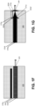
FIG. 1F is a schematic diagram representing a side view of a photonic integrated circuit employed in example embodiments of the system described herein. -
FIG. 1G is a schematic diagram representing a top view of the photonic integrated circuit shown inFIG. 1F . -
FIG. 2A is a schematic diagram representing an example embodiment of an optical modulator that can be used in the system described herein. -
FIG. 2B is a schematic diagram representing an example embodiment of the system described herein that employs a microlens array. -
FIG. 3A is a schematic diagram representing an example embodiment of a layout of a photonic integrated circuit that can be used by the system described herein. -
FIG. 3B is a schematic diagram representing another example embodiment of a layout of a photonic integrated circuit that can be used by the system described herein. -
FIG. 4 is a schematic diagram representing an example embodiment of an optical modulator of the system described herein. - According to some embodiments, the present disclosure describes methods and systems for precision laser delivery to a large number of atoms or atom-like systems for applications in quantum information processing. In some example implementations, photonic integrated circuit (PIC) systems including arrays of nanophotonic optical modulators enable high-speed simultaneous control of 1D and 2D arrays of atoms. Multiqubit gates-a core component of quantum information processing-can be applied by exciting adjacent atoms that experience a strong and coherent interaction when both atoms are in the Rydberg state. This technology potentially enables a new generation of quantum experiments beyond observation of quantum phenomena, and towards largescale control of many-body quantum systems. Arrays of nanophotonic optical modulators in PICs for high-speed simultaneous control of 1D and 2D arrays of atoms are described herein, starting with PICs based on lithium niobate-on-insulator technology, followed by active UV-visible-infrared photonics in wide-bandgap materials such as lithium niobate (LN) and aluminum nitride-on-sapphire for controlling the Rydberg transitions of individual Rubidium atoms in an array of optical traps. See Lu, Tsung-Ju, Michael Fanto, Hyeongrak Choi, Paul Thomas, Jeffrey Steidle, Sara Mouradian, Wei Kong, Di Zhu, Hyowon Moon, Karl Berggren, Jeehwan Kim, Mohammad Soltani, Stefan Preble, and Dirk Englund, "Aluminum Nitride Integrated Photonics Platform for the Ultraviolet to Visible Spectrum." Optics Express 26 (9): 11147-60 (2018).
- Among several operational requirements, the photonics need to deliver high-speed pulses at a wavelength of λ = 420 nm, optical power on the order of 100 µW at each atom, and a nanosecond switching time with >4V modulation and 40 dB extinction.
-
FIG. 1A is a schematic diagram representing an example embodiment of an optical train of asystem 100 for optically modulating a plurality of optical channels, according to some embodiments described herein. As shown inFIGS. 1A and1B , in certain embodiments, apower delivery module 130 is adapted to convert acoherent light beam 120 into a plurality of optical channels (e.g., 16 channels, of whichoptical channels FIG. 1B ). In some example embodiments, thecoherent light beam 120 is produced by acoherent light source 110 that is optically coupled to thepower delivery module 130 via anoptic fiber array 125 that is optically coupled into the plurality ofoptical channels optic fiber array 125. In certain of these embodiments, the power delivery module comprises at least one electrically controlled optical modulator adapted to modulate the at least one beam splitter (not shown).Optical system 100 also includes at least one optical modulator (150a, 150b, 150c, etc., shown inFIG. 1B ) that are optically coupled to thepower delivery module 130.Optical modulators optical channels FIG. 1B , upon modulation, optical channels 140 can be fanned out into an array ofoutput waveguides edge 159 of a photonic integrated circuit (PIC) 160, described in detail hereinbelow. The light from the array of waveguides 155a, 155b, 155c, etc. is collected by objective 189 (FIG. 1A ), e.g., a high (e.g., 0.9) numerical aperture (NA) objective. The light from the array of waveguides 155a, 155b, 155c, etc. is typically polarized in one direction, and therefore, as shown inFIG. 1A ,beam 175 produced by objective 189 includes optical signals carried bywaveguides Beam 175 can be guided bylenses pinhole 177, acleanup polarizer 180 to remove stray light polarized in the other direction, an optical cleanup filter (e.g., dichroic mirror) 182 to remove straynon-linear conversion 187, and then converted to a desired (e.g., circular) polarization with a halfwave (λ/2)plate 179 and a quarter wave (λ/4)plate 181, followed by being imaged bymirror 186 and objective 185 onto an array of trapped particles (e.g., atoms) 190 insidevacuum chamber 195. Aflip mirror 183 andalignment camera 184 are also shown inFIG. 1A . Thevacuum chamber 195 has a trappingplane 191 therein, and thevacuum chamber 195 is adapted so thatarray 190 of trapped particles is addressable. The optical train shown inFIG. 1A is configured so that each of the plurality ofoptical channels FIG. 1B , is optically coupled to at least one of the trapped particles ofarray 190.
Turning toFIG. 1C , an example embodiment of photonic integrated circuit (PIC) 160 is shown.PIC 160 includesoptical modulators output waveguides substrate 105 that is optically transparent (i.e., Abs ≤ 0.1) at wavelengths in a range of between 400 nm and 1600 nm. Suitable materials forsubstrate 105 include lithium niobate, lithium tantalate, AlxGa1-xN, silicon nitride (SiN), titanium dioxide (TiO2), barium titanate (BTO), or alumina. Lithium niobate, particularly MgO-doped lithium niobate, has excellent electro-optic properties that enable fabrication of millimeter-scale electro-optically controlled optical modulators, as described further below. As also shown inFIG. 1C , thepower delivery module 130 and the plurality ofoptical channels substrate 105. - Turning back to
FIG. 1B , theoptical modulators optical channels optical channel 140a, are labeled inFIG. 1B for clarity. As shown inFIG. 1B , in an MZI, two 50:50directional couplers input arms input arms input arm 152a that changes the refractive index (phase) oninput arm 152a due to the electro-optic (EO) effect. The phase difference changes the coupling ratio of theinput arm 152a andoutput arm 153b. Controlling the coupling ratio switches optical power output from oneoutput port 153a of the outputdirectional coupler 151b to theother output port 153b that is connected to theoutput waveguide 155a, thereby modulating the signal amplitude of each of the plurality ofoptical channels 140a. - In the present invention, optical modulators that can be employed by the systems described herein includes an MZI-coupled tunable resonator. This embodiment harnesses resonance effects to use the relatively weak electro-optic (EO) phase shift, such as the EO phase shift in aluminum nitride (AlN), to produce a much larger effect. In accordance with one or more such embodiments, in
FIG. 2A optical modulator 200 is shown. Similarly tooptical modulators FIGS. 1A-1D ,optical modulator 200 can also be adapted to modulate one of theoptical channels Optical modulator 200 comprisesresonator 215 that includesloop 210 coupled to waveguide 220. When a condition called critical coupling is satisfied, that is, when the loss inloop 210 is equal to the input, and when theloop 210 is resonant at the wavelength of theoptical input 204, optical power is completely removed fromwaveguide 204, creating a perfect off switch. To quickly turn the optical power back on, the EO effect can be used to slightly detune theloop 210 from resonance. This optical modulation scheme works well when the precise value of the wavelength is arbitrary. When the modulated wavelengths are defined by specific atomic transitions, then additional tuning is required, because, for example, random fabrication errors can affect both the resonance and critical coupling conditions, and the EO effect is not likely to fully correct for these errors. The critical coupling condition can further be tuned by replacing a coupling junction withMZI 230. Both the resonance and critical coupling conditions can be tuned with local heaters, using the thermo-optic effect that is relatively slow, typically on the order of microseconds, because of the time required for materials to heat up. As shown inFIG. 2A , the critical coupling condition is tuned by replacing the coupling with anMZI 230, onearm 250 of which is equipped withMZI heater 245.Resonator 215 is also equipped withresonator heater 247. The standard geometry for AlN tuning is shown inFIG. 2A : twoground electrodes waveguides 220a and 220 b, with anEO signal electrode 235 buffered by dielectric from thewaveguides 220a and 220b. This geometry produces a field in the z-direction, the direction of the EO effect in AlN. Current is injected throughDC electrodes resonator heater 247 andMZI heater 245 and intoground electrodes upper electrodes Diffraction grating 260 redirects the modulated output signal traveling throughwaveguide 206. -
Device 290 that includes an array of MZI-coupledtunable resonators 200a, 200b, 200c, etc. is shown inFIG. 2B . An output of each diffraction grating (not shown inFIG. 2B , labeled 260 inFIG. 2A ) can be converted to a high-NA beam usingmicrolens array 275. Each diffraction grating has itsown lens microlens array 275 to remove light that does not travel through a desired lens. Alternatively, where the arrays of optical modulators 200a, 200b, 200c, etc. is formed on transparentphotonic substrate 205, microlenses can be fabricated on the bottom surface of the substrate 205 (not shown), producing a completely integrated device. - Various embodiments of extracting modulated output from the optical modulators described herein are provided below.
- As shown in
FIG. 1D ,several PICs edges output waveguides FIG. 1E , asingle PIC 160 can be optically coupled to an array of waveguides 156a, 156b, 156c, etc. to form a2D output array 157. - As shown in
FIG. 3A , in accordance with some example embodiments, inoptical modulator array 300 that comprisesoptical modulators waveguides diffraction gratings array 310.Diffraction gratings FIG. 3B ,optical modulator array 350 is shown. Inarray 350, eachoptical modulator single pump waveguide 340 supplying optical power to eachoptical modulator single pump waveguide 340 can supply each row, with pickoff couplers (not shown) taking a fraction of the optical power for each grating-coupledmodulator - As an alternative to modulating laser beams at 420 nm on the UV-visible PICs described above, this active function can be accomplished using an already established PIC technology: silicon-on-insulator (SOI) PICs. SOI PIC technology, such as the
SOI PIC 410 shown inFIG. 4 , is available to modulate tens to hundreds ofinput waveguides 420, and SOI carrier depletion modulations can have high speed (in excess of 20 GHz) and can modulate relatively high power (in excess of 10 mW). See e.g., Elenion Technologies, New York, NY. Such SOI PICs can be used to modulate the required number of optical channels carried byinput waveguides 420 in the NIR-IR wavelength (λ = 1,100-1,700 nm). The modulatedoutput beams 430 can be used for controlling atomic optical transitions above a wavelength of 1,100 nm. For controlling UV atomic optical transitions, the modulatedoutput beams 430 can be subsequently frequency-converted to, for example, 420 nm, by coupling theSOI PIC 410 to a frequency-conversion module 440. A PIC of AlN orLN waveguides 440 can be adapted to convert an optical signal having a first frequency to an optical signal having a second frequency. WithinPIC 440, two cascaded second harmonic generation (SHG) steps from 1,680 nm to 840 nm and then to 420 nm can be performed, or, as shown inFIG. 4 , sum-frequency generation (SFG) from 1550 nm (modulated SOI PIC output 430) to 420nm output 450 can be performed using a yellow (e.g., dye) laser (input 445) at about 570 nm, or by combining approximately 1,300 nm modulatedSOI PIC output 430 with a 620 nm pump (also shown as input 445) to produce output at 420 nm (beams 450). Thewaveguides 440 can be periodically poled or width modulated for phase matching in frequency conversion. - In various embodiments of the systems described herein, the output of a PIC, positioned outside of the vacuum chamber, is imaged onto the addressable array of trapped particles located inside the vacuum chamber. This arrangement has several advantages. First, optical and electrical access to the PIC does not have to cross the vacuum seal of the vacuum chamber, improving the vacuum performance of the vacuum chamber and reducing its complexity. Second, during operation, the surface of the PIC can produce undesirable electric and magnetic fields that can negatively affect the performance of the addressable array of trapped particles. Third, during operation, the PIC can produce thermal fluctuations that can degrade the vacuum inside the vacuum chamber and the performance of the addressable array as a quantum memory.
- In some embodiments, the PIC of present invention solves the problem of a possible relative movement of the photonic hardware and the vacuum chamber that contains trapped particles. This problem can be solved by allowing the same PIC to control beams of multiple wavelengths, such as trapping (tweezer) beams and gate (control) beams, that are then jointly projected onto the atom array. Such an arrangement beneficially allows to account for small movements of the photonic hardware handling the two types of beams, so that atoms are dragged along with any small motion of the tweezer beams while remaining within the optical field of the gate beam. (In certain embodiments, vibrational movements of the PIC can be additionally damped to be less than tens of Hz so that the atoms are not heated.) Nearby wavelengths (i.e., wavelengths that are within about 20-30% of the center wavelengths) can be readily combined onto the same waveguide using wavelength division multiplexing devices, such as arrayed waveguide gratings, unbalanced Mach-Zehnder interferometer add-drop multiplexers, or resonator-based add-drop filters. For example, for controlling Rubidium (Rb) atoms, the 780 nm (D2 line) and 795 nm (D1 line) channels, together with trapping beams at about 800-810 nm can all be controlled using the same layer of the photonic integrated circuit. As described above, the two-photon Rydberg transition employs additional laser fields at 420 nm and 1013 nm. The 1013 nm wavelength can be combined with the approximately 800 nm wavelengths on the same waveguide, as single-mode waveguide operation is still assured, although the 1013 nm laser field has a slightly larger evanescent field than the 800 nm wavelengths. The 420 nm laser field is too short in wavelength to be readily controlled in the same waveguide layer.
- Referring now to
FIG. 1F and FIG. 1G , and considering a 420 nm Rydberg laser field as an example, an additional (second) layer of gate waveguides configured to carry a gate beam of a second wavelength, such as the 420 nm Rydberg laser field (only one secondlayer gate waveguide 170a is shown) can be added ontosubstrate 105, separated from the first layer trapping waveguides that are optically coupled to at least one of the trapped particles of the addressable array (i.e. waveguides 155a, b, c, etc.; only one first layer waveguide, 155d, is shown inFIG. 1F and FIG. 1G ). Secondlayer gate waveguides 170a, etc. can be disposed onPIC 160 shown inFIG. 1B . These secondlayer gate waveguides 170a, etc. can be added to the PIC during the fabrication ofsubstrate 105. As shown inFIG. 1F and FIG. 1G , secondlayer gate waveguides 170a, etc. can be separated from thefirst layer waveguides 155a, b, c, d etc., by cladding 106, as shown schematically and not to scale inFIG. 1F . In an example embodiment, the cladding can be at least 2 µm of silicon dioxide (SiO2). Two adjacent waveguides (such as 155d and 170a, shown inFIG. 1F and FIG. 1G ), each having a cross section diameter that is approximately equal to half the respective wavelength inside the waveguide material, as shown inFIG. 1F , can be optically coupled into one channel through a staggered adiabatic tapering of the two waveguides, as illustrated inFIG. 1G with respect towaveguides portion 171a of thethinner waveguide 170a begins, along the length ofwaveguide 170a, closer to edge 159 than the taperedportion 161d of thethicker waveguide 155d, as shown inFIG. 1G . This allows to evanescently transfer shorter wavelengthevanescent field 172a (e.g., blue light) from a second layer waveguide, such aswaveguide 170a, using only a single-mode section of a first layer waveguide, such aswaveguide 155d, and both the short wavelengthevanescent field 172a and the slightly larger longer wavelengthevanescent field 162d exit the PIC at the same point at theedge 159 of the PIC, thereby producing a combined multiplexed gate/trapping beam. - Accordingly, in a first example embodiment, the present invention is a system for optically modulating a plurality of optical channels. In a 1st aspect of the first example embodiment, the system comprises a power delivery module adapted to convert a coherent light beam into a plurality of optical channels; at least one optical modulator, optically coupled to the power delivery module, the at least one optical modulator adapted to optically modulate each of the plurality of the optical channels; and a vacuum chamber having a trapping plane therein, the vacuum chamber adapted to generate an addressable array of trapped particles at the trapping plane, wherein each of the plurality of optical channels is optically coupled to at least one of the trapped particles of the addressable array.
- In a 2nd aspect of the first example embodiment, the system further comprises a coherent light source optically coupled to the power delivery module.
- In a 3rd aspect of the first example embodiment, the power delivery module comprises at least one beam splitter and an optic fiber array. Other features and example features of the system are as described above with respect to the 1st through the 2nd aspects of the first example embodiments.
- In a 4th aspect of the first example embodiment, the power delivery module comprises at least one electrically controlled optical modulator adapted to modulate the at least one beam splitter. Other features and example features of the system are as described above with respect to the 1st through the 3rd aspects of the first example embodiments.
- In a 5th aspect of the first example embodiment, the at least one optical modulator is configured to modulate a signal amplitude on each of the plurality of optical channels. Other features and example features of the system are as described above with respect to the 1st through the 4th aspects of the first example embodiments.
- In a 6th aspect of the first example embodiment, the at least one optical modulator is a photonic integrated circuit (PIC). Other features and example features of the system are as described above with respect to the 1st through the 5th aspects of the first example embodiments.
- In the present invention, the at least one optical modulator comprises a plurality of electro-optically controlled Mach-Zehnder Interferometers (MZI), each of the plurality of the MZIs adapted to modulate one of the optical channels. Other features and example features of the system are as described above with respect to the 1st through the 6th aspects of the first example embodiments.
- In an 8th aspect of the first example embodiment, each of the plurality of MZIs comprise waveguides comprising a material selected from lithium niobate, lithium tantalate, AlxGa1-xN, SiN, titanium dioxide (TiO2), barium titanate (BTO), or alumina. In one example embodiment, the material is lithium niobate. Other features and example features of the system are as described above with respect to the 1st through the 7th aspects of the first example embodiments.
- In a 9th aspect of the first example embodiment, the at least one optical modulator comprises a plurality of tunable resonators, each of the plurality of tunable resonators adapted to modulate one of the optical channels. Other features and example features of the system are as described above with respect to the 1st through the 6th aspects of the first example embodiments.
- In a tenth aspect of the first example embodiment, each of the plurality of tunable resonators is a Mach-Zehnder Interferometer (MZI)-coupled resonator comprising a waveguide loop and an MZI. Other features and example features of the system are as described above with respect to the 1st through the 6th and the 9th aspect of the first example embodiments.
- In an 11th aspect of the first example embodiment, each waveguide loop includes an electro-optically controlled section adapted to modulate the waveguide loop's refractive index. Other features and example features of the system are as described above with respect to the 1st through 6th, and the 9th through the 10th aspects of the first example embodiments.
- In a 12th aspect of the first example embodiment, the tunable resonator includes a waveguide heating element adapted to modulate the waveguide loop's refractive index. Other features and example features of the system are as described above with respect to the 1st through the 6th and the 9th through the 11th aspects of the first example embodiments.
- In a 13th aspect of the first example embodiment, the MZI includes a first arm and a second arm, and the tunable resonator includes an MZI heating element adapted to modulate a refractive index of at least the first or the second arm. Other features and example features of the system are as described above with respect to the 1st through 6th and the 9th through the 12th aspects of the first example embodiments.
- In a 14th aspect of the first example embodiment, the at least one optical modulator comprises a Silicon-on-Insulator (SOI) photonic integrated circuit (PIC), said SOI PIC adapted to optically modulate each of the plurality of the optical channels. Other features and example features of the system are as described above with respect to the 1st through the 6th aspects of the first example embodiments.
- In a 15th aspect of the first example embodiment, the system further comprises a frequency-conversion module optically coupled to the SOI PIC, the frequency-conversion module adapted to convert an optical signal having a first frequency to an optical signal having a second frequency. Other features and example features of the system are as described above with respect to the 1st through the 6th and the 14th aspects of the first example embodiments.
- In a 16th aspect of the first example embodiment, the at least one optical modulator is disposed on a substrate, and wherein each of the plurality of optical channels comprises an output waveguide. Other features and example features of the system are as described above with respect to the 1st through the 15th aspects of the first example embodiments.
- In a 17th aspect of the first example embodiment, the plurality of output waveguides is configured to form a one-dimensional output array.
- Other features and example features of the system are as described above with respect to the first through the 16th aspects of the first example embodiments.
- In an 18th aspect of the first example embodiment, the system comprises a plurality of stacked optical modulators configured to form a two-dimensional output array. Other features and example features of the system are as described above with respect to the first through the 18th aspects of the first example embodiments.
- In a 19th aspect of the first example embodiment, each of the plurality of output waveguides is optically coupled to an auxiliary waveguide, the auxiliary waveguides configured to form a two-dimensional output array. Other features and example features of the system are as described above with respect to the first through the 18th aspects of the first example embodiments.
- In a 20th aspect of the first example embodiment, each output waveguide is optically coupled to a diffraction grating. Other features and example features of the system are as described above with respect to the first through the 19th aspects of the first example embodiments.
- In a 21st aspect of the first example embodiment, the diffraction gratings are configured to form a two-dimensional output array. Other features and example features of the system are as described above with respect to the first through the 21st aspects of the first example embodiments.
- In a 22nd aspect of the first example embodiment, the system further comprises a microlens array, wherein each microlens of the array is optically coupled to one of the diffraction gratings. Other features and example features of the system are as described above with respect to the first through the 21st aspects of the first example embodiments.
- In a 23rd aspect of the first example embodiment, each output waveguide is configured to carry a trapping beam of a first wavelength, and wherein the substrate further includes a plurality of gate waveguides, each trapping waveguide being optically coupled to at least one of the trapped particles of the addressable array, and each gate waveguide being configured to carry a gate beam of a second wavelength, different from the first wavelength. Other features and example features of the system are as described above with respect to the first through the 22nd aspects of the first example embodiments. In a 24th aspect of the first example embodiment, at least one output waveguide and at least one gate waveguide are configured to optically couple, thereby producing a combined wavelength-multiplexed gate/trapping beam. Other features and example features of the system are as described above with respect to the first through the 23rd aspects of the first example embodiments.
- In a second example embodiment, the present invention is a method 500 for optically modulating a plurality of optical channels. In a first aspect of the second example embodiment, the method comprises converting 510 a coherent light beam into a plurality of optical channels; delivering 520 the plurality of optical channels to at least one optical modulator, the at least one optical modulator adapted to optically modulate each of the plurality of optical channels; optically modulating 530 at least one of the plurality of optical channels; and optically coupling 540 at least one of the plurality of optical channels to at least one of a plurality of trapped particles disposed at a trapping plane of a vacuum chamber adapted to generate an addressable array of the plurality of trapped particles therein.
- Having thus described several illustrative embodiments, it is to be appreciated that various alterations, modifications, and improvements will readily occur to those skilled in the art. Such alterations, modifications, and improvements are intended to form a part of this disclosure and are intended to be within the scope of this disclosure, as disclosed in appended claims.
- While some examples presented herein involve specific combinations of functions or structural elements, it should be understood that those functions and elements may be combined in other ways according to the present disclosure to accomplish the same or different objectives. In particular, acts, elements, and features discussed in connection with one embodiment are not intended to be excluded from similar or other roles in other embodiments. Additionally, elements and components described herein may be further divided into additional components or joined together to form fewer components for performing the same functions. Accordingly, the foregoing description and attached drawings are by way of example only, and are not intended to be limiting.
Claims (15)
- A system (100) for optically modulating a plurality of optical channels, the system comprising:a power delivery module (130) adapted to convert a coherent light beam (120) into a plurality of optical channels (140);at least one optical modulator (150), optically coupled to the power delivery module (130), the at least one optical modulator (150) adapted to optically modulate each of the plurality of the optical channels (140); anda vacuum chamber (195) having a trapping plane (191) therein, the vacuum chamber (195) adapted to generate an addressable array (190) of trapped particles at the trapping plane (191), wherein each of the plurality of optical channels (140) is optically coupled to at least one of the trapped particles of the addressable array (190),chacterised in that the at least one optical modulator (150) comprises a plurality of electro-optically controlled Mach-Zehnder Interferometers, MZI, each of the plurality of the MZIs adapted to modulate one of the optical channels (140).
- The system of Claim 1, further comprising a coherent light source (110) optically coupled to the power delivery module (130).
- The system of any one of Claims 1 or 2, wherein the power delivery module (130) comprises at least one beam splitter and an optic fiber array (125).
- The system of Claim 3, wherein the power delivery module (130) comprises at least one electrically controlled optical modulator adapted to modulate the at least one beam splitter.
- The system of any one of Claims 1-4, wherein the at least one optical modulator (150) is configured to modulate a signal amplitude on each of the plurality of optical channels (140).
- The system of any one of Claims 1-5, wherein the at least one optical modulator (150) is a photonic integrated circuit, PIC, (160).
- The system of any previous Claim, wherein each of the plurality of MZIs comprise waveguides comprising a material selected from lithium niobate, lithium tantalate, AlxGa1-xN, SiN, titanium dioxide, barium titanate, or alumina; and, preferably, wherein the material is lithium niobate.
- The system of any one of Claims 1-6, wherein the at least one optical modulator (150) comprises a Silicon-on-Insulator, SOI, photonic integrated circuit, PIC (160), said SOI PIC adapted to optically modulate each of the plurality of the optical channels (140); and optionally, further comprising a frequency-conversion module optically coupled to the SOI PIC, the frequency-conversion module adapted to convert an optical signal having a first frequency to an optical signal having a second frequency.
- The system of any previous Claim, wherein the at least one optical modulator (150) is disposed on a substrate (105), and wherein each of the plurality of optical channels (140) comprises an output waveguide (155).
- The system of Claim 9, wherein the plurality of output waveguides (155) is configured to form a one-dimensional output array.
- The system of Claim 10, wherein eitherthe system comprises a plurality of stacked optical modulators configured to form a two-dimensional output array; orwherein each of the plurality of output waveguides is optically coupled to an auxiliary waveguide, the auxiliary waveguides configured to form a two-dimensional output array.
- The system of Claim 9, wherein each output waveguide is optically coupled to a diffraction grating; andoptionally, wherein the diffraction gratings are configured to form a two-dimensional output array; andfurther optionally, the system further comprising a microlens array, wherein each microlens of the array is optically coupled to one of the diffraction gratings.
- The system of any one of Claims 9-12, wherein each output waveguide (155) is configured to carry a trapping beam of a first wavelength, and wherein the substrate further includes a plurality of gate waveguides (170), each trapping waveguide being optically coupled to at least one of the trapped particles of the addressable array (190), and each gate waveguide (170) being configured to carry a gate beam of a second wavelength, different from the first wavelength; and
optionally, wherein at least one output waveguide (155) and at least one gate waveguide (170) are configured to optically couple, thereby producing a combined wavelength-multiplexed gate/trapping beam. - A method for optically modulating a plurality of optical channels, comprising:converting a coherent light beam (120) into a plurality of optical channels (140);delivering the plurality of optical channels (140) to at least one optical modulator (150), the at least one optical modulator (150) adapted to optically modulate each of the plurality of optical channels (140);optically modulating at least one of the plurality of optical channels (140); andoptically coupling at least one of the plurality of optical channels (140) to at least one of a plurality of trapped particles disposed at a trapping plane (191) of a vacuum chamber (195) adapted to generate an addressable array (190) of the plurality of trapped particles therein,characterised in thatoptically modulating at least one of the plurality of optical channels (140) includes modulating a signal amplitude on each of the plurality of optical channels (140) by electro-optically controlling a plurality of Mach-Zehnder Interferometers, MZI, each of the plurality of the MZIs modulating one of the optical channels (140).
- The method of Claim14, further including frequency converting an optical signal having a first frequency to an optical signal having a second frequency.
Applications Claiming Priority (2)
| Application Number | Priority Date | Filing Date | Title |
|---|---|---|---|
| US201962849278P | 2019-05-17 | 2019-05-17 | |
| PCT/US2020/033100 WO2020236574A1 (en) | 2019-05-17 | 2020-05-15 | System and method for multiplexed optical addressing of atomic memories |
Publications (3)
| Publication Number | Publication Date |
|---|---|
| EP3970083A1 EP3970083A1 (en) | 2022-03-23 |
| EP3970083C0 EP3970083C0 (en) | 2024-04-24 |
| EP3970083B1 true EP3970083B1 (en) | 2024-04-24 |
Family
ID=71069948
Family Applications (1)
| Application Number | Title | Priority Date | Filing Date |
|---|---|---|---|
| EP20731641.5A Active EP3970083B1 (en) | 2019-05-17 | 2020-05-15 | System and method for multiplexed optical addressing of atomic memories |
Country Status (5)
| Country | Link |
|---|---|
| US (1) | US12282242B2 (en) |
| EP (1) | EP3970083B1 (en) |
| JP (1) | JP7551654B2 (en) |
| CA (1) | CA3138309A1 (en) |
| WO (1) | WO2020236574A1 (en) |
Families Citing this family (28)
| Publication number | Priority date | Publication date | Assignee | Title |
|---|---|---|---|---|
| AU2018300240B2 (en) | 2017-07-13 | 2023-06-08 | California Institute Of Technology | Neutral atom quantum information processor |
| WO2020047444A1 (en) | 2018-08-31 | 2020-03-05 | President And Fellows Of Harvard College | Quantum computing for combinatorial optimization problems using programmable atom arrays |
| CA3112817A1 (en) | 2018-10-05 | 2020-04-09 | President And Fellows Of Harvard College | Quantum convolutional neural networks |
| US10504033B1 (en) | 2018-11-13 | 2019-12-10 | Atom Computing Inc. | Scalable neutral atom based quantum computing |
| US11995512B2 (en) | 2018-11-13 | 2024-05-28 | Atom Computing Inc. | Scalable neutral atom based quantum computing |
| US11580435B2 (en) | 2018-11-13 | 2023-02-14 | Atom Computing Inc. | Scalable neutral atom based quantum computing |
| WO2020172588A1 (en) | 2019-02-22 | 2020-08-27 | President And Fellows Of Harvard College | Large-scale uniform optical focus array generation with a phase spatial light modulator |
| CA3138309A1 (en) | 2019-05-17 | 2020-11-26 | President And Fellows Of Harvard College | System and method for multiplexed optical addressing of atomic memories |
| JP7612652B2 (en) | 2019-07-11 | 2025-01-14 | プレジデント アンド フェローズ オブ ハーバード カレッジ | Systems and methods for parallel implementation of multiqubit quantum gates |
| CN115516469B (en) | 2020-03-02 | 2026-05-01 | 原子计算公司 | Scalable neutral atom-based quantum computation |
| EP4115351A4 (en) | 2020-03-02 | 2024-05-08 | Atom Computing Inc. | Scalable neutral atom based quantum computing |
| CA3180502A1 (en) * | 2020-05-12 | 2021-11-18 | Quera Computing Incorporated | Methods and apparatus for arranging atoms in arrays |
| US11892744B2 (en) | 2020-06-10 | 2024-02-06 | Quantinuum Llc | Beam delivery system |
| CA3196700A1 (en) | 2020-11-20 | 2022-06-23 | President And Fellows Of Harvard College | Topological qubits in a quantum spin liquid |
| US11989622B2 (en) | 2020-12-01 | 2024-05-21 | ColdQuanta, Inc. | Under-resolved quantum-array state mapping |
| CA3204993A1 (en) | 2021-02-12 | 2022-08-18 | Wenchao XU | Ultrafast detector of rydberg atoms |
| US12057242B2 (en) | 2021-02-18 | 2024-08-06 | ColdQuanta, Inc. | Quantum system with multi-wavelength array trap |
| US12141655B2 (en) * | 2021-02-18 | 2024-11-12 | ColdQuanta, Inc. | Quantum system with multiple-wavelength array trap |
| CA3219612A1 (en) | 2021-05-18 | 2022-11-24 | Quera Computing Incorporated | Optical addressing methods and apparatus |
| CN115826135A (en) * | 2021-09-18 | 2023-03-21 | 华为技术有限公司 | Laser transmission device and ion trap system |
| US12353955B2 (en) | 2022-02-11 | 2025-07-08 | ColdQuanta, Inc. | Time-multiplexed superpixel-based quantum-array readout system |
| US12443870B2 (en) | 2022-03-10 | 2025-10-14 | Massachusetts Institute Of Technology | High-speed spatial light modulation and quantum control |
| EP4526813A4 (en) | 2022-05-19 | 2026-05-06 | Atom Computing Inc | DEVICES AND METHODS FOR CAVE-BASED CALCULATION |
| US12499382B2 (en) | 2022-10-13 | 2025-12-16 | International Business Machines Corporation | Selective optical tuning of qubit two-level system interactions using bandpass filters |
| US12619899B2 (en) | 2022-10-13 | 2026-05-05 | International Business Machines Corporation | Laser on-demand scrambling of two-level systems in superconducting qubits |
| US12468087B2 (en) | 2023-03-28 | 2025-11-11 | United States Of America As Represented By The Secretary Of The Air Force | Apparatus and methods for reduction of crosstalk in integrated photonics applied to addressing quantum memories |
| US12523822B2 (en) | 2023-08-22 | 2026-01-13 | United States Of America As Represented By The Secretary Of The Air Force | Apparatus and method for holding optical fiber and fiber arrays via vacuum for fiber alignment and attaching |
| KR102859166B1 (en) * | 2024-12-05 | 2025-09-12 | 서울대학교 산학협력단 | Nonlinear unitary photonic device |
Citations (2)
| Publication number | Priority date | Publication date | Assignee | Title |
|---|---|---|---|---|
| US20160161685A1 (en) | 2013-03-15 | 2016-06-09 | Finisar Corporation | Multi-channel transceiver with laser array and photonic integrated circuit |
| WO2020236574A1 (en) | 2019-05-17 | 2020-11-26 | President And Fellows Of Harvard College | System and method for multiplexed optical addressing of atomic memories |
Family Cites Families (62)
| Publication number | Priority date | Publication date | Assignee | Title |
|---|---|---|---|---|
| GB205011A (en) | 1923-02-17 | 1923-10-11 | Hermann Bollmann | Improvements in or relating to the production of lecithin from vegetable matters |
| US3872470A (en) | 1973-04-18 | 1975-03-18 | Airco Inc | Audible signal generating apparatus having selectively controlled audible output |
| US4479199A (en) | 1981-03-23 | 1984-10-23 | Friedlander Marc A | Information storage system using a photon echo medium |
| JPH01158413A (en) * | 1987-09-29 | 1989-06-21 | Nippon Telegr & Teleph Corp <Ntt> | Optical waveguide device |
| US5684621A (en) | 1995-05-08 | 1997-11-04 | Downing; Elizabeth Anne | Method and system for three-dimensional display of information based on two-photon upconversion |
| US6988058B1 (en) | 1998-12-16 | 2006-01-17 | The Regents Of The University Of California | Quantum computation with quantum dots and terahertz cavity quantum electrodynamics |
| US6332055B1 (en) | 1999-03-02 | 2001-12-18 | Sumitomo Electric Industries, Ltd. | Optical attenuator, plane waveguide type optical circuit having the same and optical attenuation system having the same |
| AU3815700A (en) | 1999-04-01 | 2000-10-23 | Optical Technologies Usa Corp | Device and method for compensating polarization mode dispersion in an optical communication system |
| WO2001076026A1 (en) | 2000-03-30 | 2001-10-11 | National Institute Of Standards And Technology ('nist') | Mode-locked pulsed laser system and method |
| FR2818838A1 (en) | 2000-12-21 | 2002-06-28 | Cit Alcatel | ADJUSTABLE DIFFERENTIAL GROUP DELAY GENERATOR AND POLARIZATION DISPERSION COMPENSATOR INCORPORATING SAME |
| US7307275B2 (en) | 2002-04-04 | 2007-12-11 | D-Wave Systems Inc. | Encoding and error suppression for superconducting quantum computers |
| US20040184711A1 (en) | 2002-06-20 | 2004-09-23 | Kenneth Bradley | Optical switches and routers and optical filters |
| JP2004045453A (en) | 2002-07-08 | 2004-02-12 | Sumitomo Electric Ind Ltd | Waveguide type optical component and method of manufacturing the same |
| US7369778B2 (en) | 2002-12-30 | 2008-05-06 | Lucent Technologies Inc. | Dispersion compensation method and apparatus |
| GB0329012D0 (en) | 2003-12-15 | 2004-01-14 | Univ Cambridge Tech | Hologram viewing device |
| JP4113161B2 (en) | 2004-07-02 | 2008-07-09 | 日本電信電話株式会社 | Optical waveguide switch |
| US7533068B2 (en) | 2004-12-23 | 2009-05-12 | D-Wave Systems, Inc. | Analog processor comprising quantum devices |
| JP4819531B2 (en) | 2006-03-01 | 2011-11-24 | 日本電信電話株式会社 | Quantum computing device and quantum computing method |
| US7870087B2 (en) | 2006-11-02 | 2011-01-11 | D-Wave Systems Inc. | Processing relational database problems using analog processors |
| US7984012B2 (en) | 2006-11-02 | 2011-07-19 | D-Wave Systems Inc. | Graph embedding techniques |
| JP5008954B2 (en) | 2006-11-28 | 2012-08-22 | 浜松ホトニクス株式会社 | Light beam generator |
| JP4994826B2 (en) | 2006-12-25 | 2012-08-08 | オリンパス株式会社 | Laser microscope |
| US7966549B2 (en) | 2007-03-01 | 2011-06-21 | Qucor Pty. Ltd. | Error corrected quantum computer |
| US7985965B2 (en) | 2007-03-29 | 2011-07-26 | Raytheon Company | Quantum computing device and method including qubit arrays of entangled states using negative refractive index lenses |
| US20080313430A1 (en) | 2007-06-12 | 2008-12-18 | Bunyk Paul I | Method and system for increasing quantum computer processing speed using digital co-processor |
| US8151174B2 (en) | 2008-02-13 | 2012-04-03 | Sunrise IP, LLC | Block modulus coding (BMC) systems and methods for block coding with non-binary modulus |
| US8229863B2 (en) | 2008-05-28 | 2012-07-24 | D-Wave Systems Inc. | Method and apparatus for evolving a quantum system using a mixed initial hamiltonian comprising both diagonal and off-diagonal terms |
| US9317473B2 (en) | 2010-12-14 | 2016-04-19 | President And Fellows Of Harvard College | Scalable room temperature quantum information processor |
| GB2498170B (en) | 2011-10-26 | 2014-01-08 | Two Trees Photonics Ltd | Frame inheritance |
| WO2014051886A1 (en) | 2012-08-22 | 2014-04-03 | President And Fellows Of Harvard College | Nanoscale scanning sensors |
| JP6143325B2 (en) | 2013-01-11 | 2017-06-07 | 大学共同利用機関法人情報・システム研究機構 | Ising model quantum computing device and Ising model quantum computing method |
| JP6094750B2 (en) | 2013-03-29 | 2017-03-15 | セイコーエプソン株式会社 | Quantum interference device, atomic oscillator, magnetic sensor, and method of manufacturing quantum interference device |
| US9858531B1 (en) | 2013-08-02 | 2018-01-02 | University Of Maryland | Fault tolerant scalable modular quantum computer architecture with an enhanced control of multi-mode couplings between trapped ion qubits |
| US10417553B2 (en) | 2014-05-01 | 2019-09-17 | Lockheed Martin Corporation | Quantum-assisted training of neural networks |
| US9355750B2 (en) | 2014-09-02 | 2016-05-31 | Wisconsin Alumni Research Foundation | System and method for optical confinement of atomic particles |
| AU2015252051B2 (en) | 2014-11-03 | 2020-10-15 | Newsouth Innovations Pty Limited | A quantum processor |
| CA2983880A1 (en) | 2015-05-05 | 2016-11-10 | Kyndi, Inc. | Quanton representation for emulating quantum-like computation on classical processors |
| EP3113084B1 (en) | 2015-06-29 | 2020-12-09 | Parity Quantum Computing GmbH | Quantum processing device and method |
| GB2542622A (en) | 2015-09-28 | 2017-03-29 | Cambridge Entpr Ltd | Method and apparatus for performing complex fourier transforms |
| JP6551149B2 (en) | 2015-10-22 | 2019-07-31 | 株式会社ジェイテクト | Fine particle capturing method and optical tweezers device |
| US10789540B2 (en) | 2016-04-18 | 2020-09-29 | D-Wave Systems Inc. | Systems and methods for embedding problems into an analog processor |
| JP2017211504A (en) | 2016-05-26 | 2017-11-30 | 住友大阪セメント株式会社 | Optical modulator |
| EP3488291B1 (en) | 2016-07-22 | 2022-06-01 | Photonic Systems, Inc. | Inherently broadband linearized electro-optic modulator with customizable performance |
| US11120357B2 (en) | 2017-03-10 | 2021-09-14 | Rigetti & Co, Inc. | Quantum approximate optimization |
| CN106980178B (en) | 2017-03-24 | 2019-05-31 | 浙江大学 | A phase-type LCoS image signal processing method and a near-eye display system |
| AU2018300240B2 (en) | 2017-07-13 | 2023-06-08 | California Institute Of Technology | Neutral atom quantum information processor |
| GB2567408B (en) | 2017-08-02 | 2020-12-02 | Dualitas Ltd | Holographic projector |
| US11100418B2 (en) | 2018-02-28 | 2021-08-24 | D-Wave Systems Inc. | Error reduction and, or, correction in analog computing including quantum processor-based computing |
| WO2020047444A1 (en) | 2018-08-31 | 2020-03-05 | President And Fellows Of Harvard College | Quantum computing for combinatorial optimization problems using programmable atom arrays |
| WO2020069253A1 (en) * | 2018-09-27 | 2020-04-02 | Massachusetts Institute Of Technology | Strained germanium silicon modulators for integrated high-speed broadband modulation |
| CA3112817A1 (en) | 2018-10-05 | 2020-04-09 | President And Fellows Of Harvard College | Quantum convolutional neural networks |
| WO2020172588A1 (en) | 2019-02-22 | 2020-08-27 | President And Fellows Of Harvard College | Large-scale uniform optical focus array generation with a phase spatial light modulator |
| JP7612652B2 (en) | 2019-07-11 | 2025-01-14 | プレジデント アンド フェローズ オブ ハーバード カレッジ | Systems and methods for parallel implementation of multiqubit quantum gates |
| WO2021141918A1 (en) | 2020-01-06 | 2021-07-15 | President And Fellows Of Harvard College | System and method for quantum sampling from a probability distribution |
| US12321821B2 (en) | 2020-10-30 | 2025-06-03 | Massachusetts Institute Of Technology | All-connected, cavity-mediated quantum computing with local quantum processors |
| CA3196700A1 (en) | 2020-11-20 | 2022-06-23 | President And Fellows Of Harvard College | Topological qubits in a quantum spin liquid |
| WO2022132388A2 (en) | 2020-11-20 | 2022-06-23 | President And Fellows Of Harvard College | Topological qubits in a quantum spin liquid |
| CA3204993A1 (en) | 2021-02-12 | 2022-08-18 | Wenchao XU | Ultrafast detector of rydberg atoms |
| WO2023287503A2 (en) | 2021-05-27 | 2023-01-19 | President And Fellows Of Harvard College | Fault-tolerant quantum computation |
| WO2023080936A2 (en) | 2021-07-16 | 2023-05-11 | President And Fellows Of Harvard College | Dispersive optics for scalable raman driving of hyperfine qubits |
| EP4381429A2 (en) | 2021-08-03 | 2024-06-12 | President and Fellows of Harvard College | Dynamically reconfigurable architectures for quantum information and simulation |
| JP2025527074A (en) | 2022-07-01 | 2025-08-19 | プレジデント アンド フェローズ オブ ハーバード カレッジ | Modular Rydberg Architecture for Fault-Tolerant Quantum Computing |
-
2020
- 2020-05-15 CA CA3138309A patent/CA3138309A1/en active Pending
- 2020-05-15 JP JP2021568239A patent/JP7551654B2/en active Active
- 2020-05-15 EP EP20731641.5A patent/EP3970083B1/en active Active
- 2020-05-15 WO PCT/US2020/033100 patent/WO2020236574A1/en not_active Ceased
- 2020-05-15 US US17/611,679 patent/US12282242B2/en active Active
Patent Citations (2)
| Publication number | Priority date | Publication date | Assignee | Title |
|---|---|---|---|---|
| US20160161685A1 (en) | 2013-03-15 | 2016-06-09 | Finisar Corporation | Multi-channel transceiver with laser array and photonic integrated circuit |
| WO2020236574A1 (en) | 2019-05-17 | 2020-11-26 | President And Fellows Of Harvard College | System and method for multiplexed optical addressing of atomic memories |
Non-Patent Citations (13)
| Title |
|---|
| ANONYMOUS: "Electro-optic modulator", WIKIPEDIA, 14 May 2019 (2019-05-14), pages 1 - 4, XP093257239 |
| BRUZEWICZ COLIN D. ET AL: "Trapped-ion quantum computing: Progress and challenges", APPLIED PHYSICS REVIEWS, AMERICAN INSTITUTE OF PHYSICS, 2 HUNTINGTON QUADRANGLE, MELVILLE, NY 11747, vol. 6, no. 2, 29 May 2019 (2019-05-29), 2 Huntington Quadrangle, Melville, NY 11747 , XP012238166, DOI: 10.1063/1.5088164 |
| D15: US PROVISIONAL APPLICATION "MULTIPLEXED OPTICAL ADDRESSING OF ATOMIC MEMORIES" |
| D16: STRUCTURE OF CLAIM 1 |
| KIELPINSKI D. ET AL: "Integrated optics architecture for trapped-ion quantum information processing", QUANTUM INFORMATION PROCESSING, SPRINGER US, NEW YORK, vol. 15, no. 12, 23 November 2015 (2015-11-23), New York, pages 5315 - 5338, XP036105505, ISSN: 1570-0755, DOI: 10.1007/s11128-015-1162-2 |
| M SAFFMAN: "Quantum computing with atomic qubits and Rydberg interactions: progress and challenges", JOURNAL OF PHYSICS B, ATOMIC MOLECULAR AND OPTICAL PHYSICS, INSTITUTE OF PHYSICS PUBLISHING, BRISTOL, GB, vol. 49, no. 20, 4 October 2016 (2016-10-04), GB , pages 202001, XP020309686, ISSN: 0953-4075, DOI: 10.1088/0953-4075/49/20/202001 |
| QI YIFAN, LI YANG: "Integrated lithium niobate photonics", NANOPHOTONICS, DE GRUYTER, DE, vol. 9, no. 6, 1 June 2020 (2020-06-01), DE , pages 1287 - 1320, XP093042016, ISSN: 2192-8606, DOI: 10.1515/nanoph-2020-0013 |
| QUINT STEPHAN: "Formung von Laserlichtimpulsen für die Quanteninformationsverarbeitung mit 40Ca+", DIPLOMARBEIT, INSTITUT FÜR PHYSIK JOHANNES GUTENBERG-UNIVERSITÄT MAINZ, 1 May 2011 (2011-05-01), pages 1 - 94, XP093257215 |
| RICCARDO MARCHETTI ET AL.: "Coupling strategies for silicon photonics integrated chips [Invited]", PHOTONICS RESEARCH, vol. 7, February 2019 (2019-02-01), pages 2, XP055893568, DOI: 10.1364/PRJ.7.000201 |
| RICKERT JULIAN: "Simultaneous and individual ion addressing for quantum information processing", LEOPOLD-FRANZENS-UNIVERSITÄT INNSBRUCK, 1 November 2018 (2018-11-01), pages 1 - 89, XP055979503, Retrieved from the Internet <URL:https://www.quantumoptics.at/images/publications/diploma/master_rickert.pdf> [retrieved on 20221109] |
| S. DEBNATH ET AL: "Demonstration of a small programmable quantum computer with atomic qubits", NATURE, vol. 536, no. 7614, 1 August 2016 (2016-08-01), pages 63 - 66, XP055451676, DOI: 10.1038/nature18648 |
| T. G. TIECKE ET AL: "Nanophotonic quantum phase switch with a single atom", NATURE, vol. 508, no. 7495, pages 241 - 244, XP055572992, DOI: 10.1038/nature13188 |
| WANG CHENG ET AL: "Second harmonic generation in nano-structured thin-film lithium niobate waveguides", OPTICS EXPRESS, OPTICAL SOCIETY OF AMERICA, US, vol. 25, no. 6, 20 March 2017 (2017-03-20), US, pages 1 - 11, XP093257224, ISSN: 1094-4087, DOI: 10.1364/OE.25.006963 |
Also Published As
| Publication number | Publication date |
|---|---|
| EP3970083A1 (en) | 2022-03-23 |
| WO2020236574A1 (en) | 2020-11-26 |
| JP7551654B2 (en) | 2024-09-17 |
| US12282242B2 (en) | 2025-04-22 |
| CA3138309A1 (en) | 2020-11-26 |
| EP3970083C0 (en) | 2024-04-24 |
| US20220197102A1 (en) | 2022-06-23 |
| JP2022532234A (en) | 2022-07-13 |
Similar Documents
| Publication | Publication Date | Title |
|---|---|---|
| JP7551654B2 (en) | Systems and methods for multiplexed optical addressing of atomic memories | |
| JP2022532234A5 (en) | ||
| Eldada | Optical communication components | |
| Boes et al. | Status and potential of lithium niobate on insulator (LNOI) for photonic integrated circuits | |
| Janner et al. | Micro‐structured integrated electro‐optic LiNbO3 modulators | |
| US11429009B2 (en) | Integrated electro-optic devices for classical and quantum microwave photonics | |
| US20020181067A1 (en) | Electro-optic switching assembly and method | |
| US20050002605A1 (en) | Light control element and light control device | |
| JPH10509246A (en) | Controllable beam director using polarized structures | |
| WO2004023174A2 (en) | Photorefractive devices | |
| US12443870B2 (en) | High-speed spatial light modulation and quantum control | |
| Poveda et al. | Semiconductor optical waveguide devices modulated by surface acoustic waves | |
| Kielpinski et al. | Integrated optics architecture for trapped-ion quantum information processing | |
| US6614947B1 (en) | Digital optical switch using an integrated mach-zehnder interferometer having a movable phase shifter | |
| Fong et al. | Tunable optical coupler controlled by optical gradient forces | |
| JP2765529B2 (en) | Waveguide type optical device | |
| Mancinelli | Linear and non linear coupling effects in sequence of microresonators | |
| Nishihara et al. | Optical integrated circuits | |
| US6563965B1 (en) | Analog optical switch using an integrated Mach-Zehnder interferometer having a moveable phase shifter | |
| Lai et al. | On-chip nonvolatile and erasable silicon waveguide filter based on a low-loss phase-change material | |
| JP2015191111A (en) | Optical add/drop apparatus, optical switch and manufacturing method | |
| Ghoumid et al. | Wavelength-Selective Ti: LiNbO $ _ {3} $ Multiple Y-Branch Coupler Based on Focused Ion Beam Milled Bragg Reflectors | |
| Poon et al. | Photonics filters, switches and subsystems for next-generation optical networks | |
| Abe et al. | A silicon microring resonator with a nanolatch mechanism | |
| Gautam | Silicon microring resonator loaded mach-zehnder interferometer for low power optical modulation, switching and bio-sensing |
Legal Events
| Date | Code | Title | Description |
|---|---|---|---|
| STAA | Information on the status of an ep patent application or granted ep patent |
Free format text: STATUS: UNKNOWN |
|
| STAA | Information on the status of an ep patent application or granted ep patent |
Free format text: STATUS: THE INTERNATIONAL PUBLICATION HAS BEEN MADE |
|
| PUAI | Public reference made under article 153(3) epc to a published international application that has entered the european phase |
Free format text: ORIGINAL CODE: 0009012 |
|
| STAA | Information on the status of an ep patent application or granted ep patent |
Free format text: STATUS: REQUEST FOR EXAMINATION WAS MADE |
|
| 17P | Request for examination filed |
Effective date: 20211117 |
|
| AK | Designated contracting states |
Kind code of ref document: A1 Designated state(s): AL AT BE BG CH CY CZ DE DK EE ES FI FR GB GR HR HU IE IS IT LI LT LU LV MC MK MT NL NO PL PT RO RS SE SI SK SM TR |
|
| REG | Reference to a national code |
Ref country code: DE Ref legal event code: R079 Free format text: PREVIOUS MAIN CLASS: G06N0010000000 Ipc: G02F0001000000 Ref document number: 602020029605 Country of ref document: DE |
|
| GRAP | Despatch of communication of intention to grant a patent |
Free format text: ORIGINAL CODE: EPIDOSNIGR1 |
|
| STAA | Information on the status of an ep patent application or granted ep patent |
Free format text: STATUS: GRANT OF PATENT IS INTENDED |
|
| RIC1 | Information provided on ipc code assigned before grant |
Ipc: G06N 10/00 20220101ALN20231017BHEP Ipc: G02F 1/00 20060101AFI20231017BHEP |
|
| DAV | Request for validation of the european patent (deleted) | ||
| DAX | Request for extension of the european patent (deleted) | ||
| INTG | Intention to grant announced |
Effective date: 20231102 |
|
| GRAS | Grant fee paid |
Free format text: ORIGINAL CODE: EPIDOSNIGR3 |
|
| TPAC | Observations filed by third parties |
Free format text: ORIGINAL CODE: EPIDOSNTIPA |
|
| GRAA | (expected) grant |
Free format text: ORIGINAL CODE: 0009210 |
|
| STAA | Information on the status of an ep patent application or granted ep patent |
Free format text: STATUS: THE PATENT HAS BEEN GRANTED |
|
| AK | Designated contracting states |
Kind code of ref document: B1 Designated state(s): AL AT BE BG CH CY CZ DE DK EE ES FI FR GB GR HR HU IE IS IT LI LT LU LV MC MK MT NL NO PL PT RO RS SE SI SK SM TR |
|
| REG | Reference to a national code |
Ref country code: GB Ref legal event code: FG4D |
|
| REG | Reference to a national code |
Ref country code: CH Ref legal event code: EP |
|
| REG | Reference to a national code |
Ref country code: DE Ref legal event code: R096 Ref document number: 602020029605 Country of ref document: DE |
|
| REG | Reference to a national code |
Ref country code: IE Ref legal event code: FG4D |
|
| U01 | Request for unitary effect filed |
Effective date: 20240520 |
|
| U07 | Unitary effect registered |
Designated state(s): AT BE BG DE DK EE FI FR IT LT LU LV MT NL PT SE SI Effective date: 20240529 |
|
| U20 | Renewal fee for the european patent with unitary effect paid |
Year of fee payment: 5 Effective date: 20240528 |
|
| PG25 | Lapsed in a contracting state [announced via postgrant information from national office to epo] |
Ref country code: IS Free format text: LAPSE BECAUSE OF FAILURE TO SUBMIT A TRANSLATION OF THE DESCRIPTION OR TO PAY THE FEE WITHIN THE PRESCRIBED TIME-LIMIT Effective date: 20240824 |
|
| PG25 | Lapsed in a contracting state [announced via postgrant information from national office to epo] |
Ref country code: HR Free format text: LAPSE BECAUSE OF FAILURE TO SUBMIT A TRANSLATION OF THE DESCRIPTION OR TO PAY THE FEE WITHIN THE PRESCRIBED TIME-LIMIT Effective date: 20240424 |
|
| PG25 | Lapsed in a contracting state [announced via postgrant information from national office to epo] |
Ref country code: GR Free format text: LAPSE BECAUSE OF FAILURE TO SUBMIT A TRANSLATION OF THE DESCRIPTION OR TO PAY THE FEE WITHIN THE PRESCRIBED TIME-LIMIT Effective date: 20240725 |
|
| PG25 | Lapsed in a contracting state [announced via postgrant information from national office to epo] |
Ref country code: ES Free format text: LAPSE BECAUSE OF FAILURE TO SUBMIT A TRANSLATION OF THE DESCRIPTION OR TO PAY THE FEE WITHIN THE PRESCRIBED TIME-LIMIT Effective date: 20240424 |
|
| PG25 | Lapsed in a contracting state [announced via postgrant information from national office to epo] |
Ref country code: PL Free format text: LAPSE BECAUSE OF FAILURE TO SUBMIT A TRANSLATION OF THE DESCRIPTION OR TO PAY THE FEE WITHIN THE PRESCRIBED TIME-LIMIT Effective date: 20240424 |
|
| PG25 | Lapsed in a contracting state [announced via postgrant information from national office to epo] |
Ref country code: PL Free format text: LAPSE BECAUSE OF FAILURE TO SUBMIT A TRANSLATION OF THE DESCRIPTION OR TO PAY THE FEE WITHIN THE PRESCRIBED TIME-LIMIT Effective date: 20240424 Ref country code: NO Free format text: LAPSE BECAUSE OF FAILURE TO SUBMIT A TRANSLATION OF THE DESCRIPTION OR TO PAY THE FEE WITHIN THE PRESCRIBED TIME-LIMIT Effective date: 20240724 Ref country code: IS Free format text: LAPSE BECAUSE OF FAILURE TO SUBMIT A TRANSLATION OF THE DESCRIPTION OR TO PAY THE FEE WITHIN THE PRESCRIBED TIME-LIMIT Effective date: 20240824 Ref country code: HR Free format text: LAPSE BECAUSE OF FAILURE TO SUBMIT A TRANSLATION OF THE DESCRIPTION OR TO PAY THE FEE WITHIN THE PRESCRIBED TIME-LIMIT Effective date: 20240424 Ref country code: GR Free format text: LAPSE BECAUSE OF FAILURE TO SUBMIT A TRANSLATION OF THE DESCRIPTION OR TO PAY THE FEE WITHIN THE PRESCRIBED TIME-LIMIT Effective date: 20240725 Ref country code: ES Free format text: LAPSE BECAUSE OF FAILURE TO SUBMIT A TRANSLATION OF THE DESCRIPTION OR TO PAY THE FEE WITHIN THE PRESCRIBED TIME-LIMIT Effective date: 20240424 Ref country code: RS Free format text: LAPSE BECAUSE OF FAILURE TO SUBMIT A TRANSLATION OF THE DESCRIPTION OR TO PAY THE FEE WITHIN THE PRESCRIBED TIME-LIMIT Effective date: 20240724 |
|
| REG | Reference to a national code |
Ref country code: CH Ref legal event code: PL |
|
| PG25 | Lapsed in a contracting state [announced via postgrant information from national office to epo] |
Ref country code: CZ Free format text: LAPSE BECAUSE OF FAILURE TO SUBMIT A TRANSLATION OF THE DESCRIPTION OR TO PAY THE FEE WITHIN THE PRESCRIBED TIME-LIMIT Effective date: 20240424 |
|
| REG | Reference to a national code |
Ref country code: DE Ref legal event code: R026 Ref document number: 602020029605 Country of ref document: DE |
|
| PG25 | Lapsed in a contracting state [announced via postgrant information from national office to epo] |
Ref country code: SK Free format text: LAPSE BECAUSE OF FAILURE TO SUBMIT A TRANSLATION OF THE DESCRIPTION OR TO PAY THE FEE WITHIN THE PRESCRIBED TIME-LIMIT Effective date: 20240424 Ref country code: RO Free format text: LAPSE BECAUSE OF FAILURE TO SUBMIT A TRANSLATION OF THE DESCRIPTION OR TO PAY THE FEE WITHIN THE PRESCRIBED TIME-LIMIT Effective date: 20240424 |
|
| PG25 | Lapsed in a contracting state [announced via postgrant information from national office to epo] |
Ref country code: SM Free format text: LAPSE BECAUSE OF FAILURE TO SUBMIT A TRANSLATION OF THE DESCRIPTION OR TO PAY THE FEE WITHIN THE PRESCRIBED TIME-LIMIT Effective date: 20240424 |
|
| PG25 | Lapsed in a contracting state [announced via postgrant information from national office to epo] |
Ref country code: SM Free format text: LAPSE BECAUSE OF FAILURE TO SUBMIT A TRANSLATION OF THE DESCRIPTION OR TO PAY THE FEE WITHIN THE PRESCRIBED TIME-LIMIT Effective date: 20240424 Ref country code: SK Free format text: LAPSE BECAUSE OF FAILURE TO SUBMIT A TRANSLATION OF THE DESCRIPTION OR TO PAY THE FEE WITHIN THE PRESCRIBED TIME-LIMIT Effective date: 20240424 Ref country code: RO Free format text: LAPSE BECAUSE OF FAILURE TO SUBMIT A TRANSLATION OF THE DESCRIPTION OR TO PAY THE FEE WITHIN THE PRESCRIBED TIME-LIMIT Effective date: 20240424 Ref country code: CZ Free format text: LAPSE BECAUSE OF FAILURE TO SUBMIT A TRANSLATION OF THE DESCRIPTION OR TO PAY THE FEE WITHIN THE PRESCRIBED TIME-LIMIT Effective date: 20240424 Ref country code: CH Free format text: LAPSE BECAUSE OF NON-PAYMENT OF DUE FEES Effective date: 20240531 Ref country code: MC Free format text: LAPSE BECAUSE OF FAILURE TO SUBMIT A TRANSLATION OF THE DESCRIPTION OR TO PAY THE FEE WITHIN THE PRESCRIBED TIME-LIMIT Effective date: 20240424 |
|
| PLBI | Opposition filed |
Free format text: ORIGINAL CODE: 0009260 |
|
| PLAX | Notice of opposition and request to file observation + time limit sent |
Free format text: ORIGINAL CODE: EPIDOSNOBS2 |
|
| 26 | Opposition filed |
Opponent name: SCHWARZ & PARTNER PATENTANWAELTE GMBH Effective date: 20250124 |
|
| PG25 | Lapsed in a contracting state [announced via postgrant information from national office to epo] |
Ref country code: IE Free format text: LAPSE BECAUSE OF NON-PAYMENT OF DUE FEES Effective date: 20240515 |
|
| PLBB | Reply of patent proprietor to notice(s) of opposition received |
Free format text: ORIGINAL CODE: EPIDOSNOBS3 |
|
| U20 | Renewal fee for the european patent with unitary effect paid |
Year of fee payment: 6 Effective date: 20250527 |
|
| PGFP | Annual fee paid to national office [announced via postgrant information from national office to epo] |
Ref country code: GB Payment date: 20250527 Year of fee payment: 6 |
|
| PG25 | Lapsed in a contracting state [announced via postgrant information from national office to epo] |
Ref country code: CY Free format text: LAPSE BECAUSE OF FAILURE TO SUBMIT A TRANSLATION OF THE DESCRIPTION OR TO PAY THE FEE WITHIN THE PRESCRIBED TIME-LIMIT; INVALID AB INITIO Effective date: 20200515 |
|
| PG25 | Lapsed in a contracting state [announced via postgrant information from national office to epo] |
Ref country code: HU Free format text: LAPSE BECAUSE OF FAILURE TO SUBMIT A TRANSLATION OF THE DESCRIPTION OR TO PAY THE FEE WITHIN THE PRESCRIBED TIME-LIMIT; INVALID AB INITIO Effective date: 20200515 |
|
| U1N | Appointed representative for the unitary patent procedure changed after the registration of the unitary effect |
Representative=s name: PETERREINS SCHLEY; DE |