EP3968389A1 - Unipolar power transistor and rc snubber - Google Patents
Unipolar power transistor and rc snubber Download PDFInfo
- Publication number
- EP3968389A1 EP3968389A1 EP21020444.2A EP21020444A EP3968389A1 EP 3968389 A1 EP3968389 A1 EP 3968389A1 EP 21020444 A EP21020444 A EP 21020444A EP 3968389 A1 EP3968389 A1 EP 3968389A1
- Authority
- EP
- European Patent Office
- Prior art keywords
- power transistor
- snubber
- unipolar power
- layer
- resistor
- Prior art date
- Legal status (The legal status is an assumption and is not a legal conclusion. Google has not performed a legal analysis and makes no representation as to the accuracy of the status listed.)
- Pending
Links
- 239000000758 substrate Substances 0.000 claims abstract description 50
- 239000003990 capacitor Substances 0.000 claims abstract description 46
- 239000004065 semiconductor Substances 0.000 claims abstract description 43
- 229910021420 polycrystalline silicon Inorganic materials 0.000 claims abstract description 31
- 229920005591 polysilicon Polymers 0.000 claims abstract description 31
- XUIMIQQOPSSXEZ-UHFFFAOYSA-N Silicon Chemical group [Si] XUIMIQQOPSSXEZ-UHFFFAOYSA-N 0.000 claims abstract description 25
- 239000000463 material Substances 0.000 claims description 39
- HBMJWWWQQXIZIP-UHFFFAOYSA-N silicon carbide Chemical compound [Si+]#[C-] HBMJWWWQQXIZIP-UHFFFAOYSA-N 0.000 claims description 22
- 229910010271 silicon carbide Inorganic materials 0.000 claims description 22
- 230000005669 field effect Effects 0.000 claims description 7
- 229910002601 GaN Inorganic materials 0.000 claims description 5
- JMASRVWKEDWRBT-UHFFFAOYSA-N Gallium nitride Chemical compound [Ga]#N JMASRVWKEDWRBT-UHFFFAOYSA-N 0.000 claims description 5
- 239000010410 layer Substances 0.000 description 88
- 230000010355 oscillation Effects 0.000 description 31
- 238000000034 method Methods 0.000 description 9
- 229910052751 metal Inorganic materials 0.000 description 7
- 239000004020 conductor Substances 0.000 description 6
- 239000002184 metal Substances 0.000 description 5
- 239000003989 dielectric material Substances 0.000 description 4
- 230000003071 parasitic effect Effects 0.000 description 4
- VYPSYNLAJGMNEJ-UHFFFAOYSA-N Silicium dioxide Chemical compound O=[Si]=O VYPSYNLAJGMNEJ-UHFFFAOYSA-N 0.000 description 3
- 230000008901 benefit Effects 0.000 description 3
- 230000006870 function Effects 0.000 description 3
- 238000012986 modification Methods 0.000 description 3
- 230000004048 modification Effects 0.000 description 3
- 230000001960 triggered effect Effects 0.000 description 3
- 229910016570 AlCu Inorganic materials 0.000 description 2
- IJGRMHOSHXDMSA-UHFFFAOYSA-N Atomic nitrogen Chemical compound N#N IJGRMHOSHXDMSA-UHFFFAOYSA-N 0.000 description 2
- BOTDANWDWHJENH-UHFFFAOYSA-N Tetraethyl orthosilicate Chemical compound CCO[Si](OCC)(OCC)OCC BOTDANWDWHJENH-UHFFFAOYSA-N 0.000 description 2
- 230000004075 alteration Effects 0.000 description 2
- WPPDFTBPZNZZRP-UHFFFAOYSA-N aluminum copper Chemical compound [Al].[Cu] WPPDFTBPZNZZRP-UHFFFAOYSA-N 0.000 description 2
- 238000005229 chemical vapour deposition Methods 0.000 description 2
- 238000013016 damping Methods 0.000 description 2
- 238000010586 diagram Methods 0.000 description 2
- 239000007943 implant Substances 0.000 description 2
- 238000004519 manufacturing process Methods 0.000 description 2
- 239000007769 metal material Substances 0.000 description 2
- -1 SiCN Chemical compound 0.000 description 1
- 230000002411 adverse Effects 0.000 description 1
- QVGXLLKOCUKJST-UHFFFAOYSA-N atomic oxygen Chemical compound [O] QVGXLLKOCUKJST-UHFFFAOYSA-N 0.000 description 1
- 238000004590 computer program Methods 0.000 description 1
- 230000001419 dependent effect Effects 0.000 description 1
- 239000002019 doping agent Substances 0.000 description 1
- 238000004146 energy storage Methods 0.000 description 1
- 230000010354 integration Effects 0.000 description 1
- 239000011229 interlayer Substances 0.000 description 1
- 229910052757 nitrogen Inorganic materials 0.000 description 1
- 239000001301 oxygen Substances 0.000 description 1
- 229910052760 oxygen Inorganic materials 0.000 description 1
- 235000012239 silicon dioxide Nutrition 0.000 description 1
- 239000000377 silicon dioxide Substances 0.000 description 1
- 229910052814 silicon oxide Inorganic materials 0.000 description 1
- 230000002123 temporal effect Effects 0.000 description 1
- 239000011800 void material Substances 0.000 description 1
Images



Classifications
-
- H—ELECTRICITY
- H02—GENERATION; CONVERSION OR DISTRIBUTION OF ELECTRIC POWER
- H02H—EMERGENCY PROTECTIVE CIRCUIT ARRANGEMENTS
- H02H9/00—Emergency protective circuit arrangements for limiting excess current or voltage without disconnection
- H02H9/04—Emergency protective circuit arrangements for limiting excess current or voltage without disconnection responsive to excess voltage
-
- H—ELECTRICITY
- H10—SEMICONDUCTOR DEVICES; ELECTRIC SOLID-STATE DEVICES NOT OTHERWISE PROVIDED FOR
- H10D—INORGANIC ELECTRIC SEMICONDUCTOR DEVICES
- H10D30/00—Field-effect transistors [FET]
- H10D30/60—Insulated-gate field-effect transistors [IGFET]
- H10D30/64—Double-diffused metal-oxide semiconductor [DMOS] FETs
- H10D30/66—Vertical DMOS [VDMOS] FETs
-
- H—ELECTRICITY
- H10—SEMICONDUCTOR DEVICES; ELECTRIC SOLID-STATE DEVICES NOT OTHERWISE PROVIDED FOR
- H10D—INORGANIC ELECTRIC SEMICONDUCTOR DEVICES
- H10D1/00—Resistors, capacitors or inductors
- H10D1/40—Resistors
- H10D1/47—Resistors having no potential barriers
-
- H—ELECTRICITY
- H10—SEMICONDUCTOR DEVICES; ELECTRIC SOLID-STATE DEVICES NOT OTHERWISE PROVIDED FOR
- H10D—INORGANIC ELECTRIC SEMICONDUCTOR DEVICES
- H10D1/00—Resistors, capacitors or inductors
- H10D1/60—Capacitors
- H10D1/62—Capacitors having potential barriers
-
- H—ELECTRICITY
- H10—SEMICONDUCTOR DEVICES; ELECTRIC SOLID-STATE DEVICES NOT OTHERWISE PROVIDED FOR
- H10D—INORGANIC ELECTRIC SEMICONDUCTOR DEVICES
- H10D30/00—Field-effect transistors [FET]
- H10D30/60—Insulated-gate field-effect transistors [IGFET]
- H10D30/64—Double-diffused metal-oxide semiconductor [DMOS] FETs
- H10D30/66—Vertical DMOS [VDMOS] FETs
- H10D30/668—Vertical DMOS [VDMOS] FETs having trench gate electrodes, e.g. UMOS transistors
-
- H—ELECTRICITY
- H10—SEMICONDUCTOR DEVICES; ELECTRIC SOLID-STATE DEVICES NOT OTHERWISE PROVIDED FOR
- H10D—INORGANIC ELECTRIC SEMICONDUCTOR DEVICES
- H10D30/00—Field-effect transistors [FET]
- H10D30/80—FETs having rectifying junction gate electrodes
- H10D30/83—FETs having PN junction gate electrodes
- H10D30/831—Vertical FETs having PN junction gate electrodes
-
- H—ELECTRICITY
- H10—SEMICONDUCTOR DEVICES; ELECTRIC SOLID-STATE DEVICES NOT OTHERWISE PROVIDED FOR
- H10D—INORGANIC ELECTRIC SEMICONDUCTOR DEVICES
- H10D62/00—Semiconductor bodies, or regions thereof, of devices having potential barriers
- H10D62/80—Semiconductor bodies, or regions thereof, of devices having potential barriers characterised by the materials
- H10D62/83—Semiconductor bodies, or regions thereof, of devices having potential barriers characterised by the materials being Group IV materials, e.g. B-doped Si or undoped Ge
- H10D62/832—Semiconductor bodies, or regions thereof, of devices having potential barriers characterised by the materials being Group IV materials, e.g. B-doped Si or undoped Ge being Group IV materials comprising two or more elements, e.g. SiGe
- H10D62/8325—Silicon carbide
-
- H—ELECTRICITY
- H10—SEMICONDUCTOR DEVICES; ELECTRIC SOLID-STATE DEVICES NOT OTHERWISE PROVIDED FOR
- H10D—INORGANIC ELECTRIC SEMICONDUCTOR DEVICES
- H10D62/00—Semiconductor bodies, or regions thereof, of devices having potential barriers
- H10D62/80—Semiconductor bodies, or regions thereof, of devices having potential barriers characterised by the materials
- H10D62/85—Semiconductor bodies, or regions thereof, of devices having potential barriers characterised by the materials being Group III-V materials, e.g. GaAs
- H10D62/8503—Nitride Group III-V materials, e.g. AlN or GaN
-
- H—ELECTRICITY
- H10—SEMICONDUCTOR DEVICES; ELECTRIC SOLID-STATE DEVICES NOT OTHERWISE PROVIDED FOR
- H10D—INORGANIC ELECTRIC SEMICONDUCTOR DEVICES
- H10D84/00—Integrated devices formed in or on semiconductor substrates that comprise only semiconducting layers, e.g. on Si wafers or on GaAs-on-Si wafers
- H10D84/101—Integrated devices comprising main components and built-in components, e.g. IGBT having built-in freewheel diode
- H10D84/141—VDMOS having built-in components
-
- H—ELECTRICITY
- H10—SEMICONDUCTOR DEVICES; ELECTRIC SOLID-STATE DEVICES NOT OTHERWISE PROVIDED FOR
- H10D—INORGANIC ELECTRIC SEMICONDUCTOR DEVICES
- H10D84/00—Integrated devices formed in or on semiconductor substrates that comprise only semiconducting layers, e.g. on Si wafers or on GaAs-on-Si wafers
- H10D84/80—Integrated devices formed in or on semiconductor substrates that comprise only semiconducting layers, e.g. on Si wafers or on GaAs-on-Si wafers characterised by the integration of at least one component covered by groups H10D12/00 or H10D30/00, e.g. integration of IGFETs
- H10D84/811—Combinations of field-effect devices and one or more diodes, capacitors or resistors
Definitions
- the present disclosure relates to the field of dampening oscillations within semiconductor devices.
- transistors such as silicon carbide metal-oxide-semiconductor field-effect transistors (SiC MOSFETS) and other types of transistors, may be used for applications in high power and high voltage range use, such as in traction and wind energy applications. These types of applications may utilize high currents and large power modules or parallel connection modules. Operation of these transistors may result in relatively high commutation inductances, such as in the range of 20nH - 100nH per commutation path. If a load current in one of these transistors is switched off quickly, commutation oscillations may be triggered. The commutation oscillations can result in electromagnetic interference and/or failure to comply with electromagnetic interference limits. Such commutation oscillations are undesirable for applications that utilize high load currents.
- SiC MOSFETS silicon carbide metal-oxide-semiconductor field-effect transistors
- an apparatus comprising a unipolar power transistor.
- the apparatus comprises an RC snubber coupled in parallel within the unipolar power transistor.
- the RC snubber and the unipolar power transistor are formed monolithically on a semiconductor substrate.
- the RC snubber comprises a capacitor.
- the capacitor is between a poly silicon structure and the semiconductor substrate.
- the capacitor comprises a p-n junction.
- the RC snubber comprises a resistor.
- the resistor is between a source of the unipolar power transistor and a first layer forming the capacitor.
- transistors such as silicon carbide metal-oxide-semiconductor field-effect transistors (SiC MOSFETS), silicon carbide junction gate field-effect transistors (SiC JFET), unipolar power transistors, etc.
- SiC MOSFETS silicon carbide metal-oxide-semiconductor field-effect transistors
- SiC JFET silicon carbide junction gate field-effect transistors
- unipolar power transistors may be used for various applications, such as for switching in high powered and/or high voltage applications.
- commutation oscillations can be triggered, thus causing undesirable oscillation energy within the device that can negatively affect operation of the device.
- the commutation oscillations may be triggered when the transistor is used as a power transistor with high voltages (e.g., voltages over 600 volts) such that switching off the transistor is so rapid that commutation oscillations result.
- These commutation oscillations can be high-frequency LC oscillations that negatively affect operation of the device.
- the commutation oscillations can result in electromagnetic interference that impact the correct operation of the device.
- electromagnetic interference a transistor may be initially in an off state. While in the on state, a drain and source voltage of the transistor is low. When the transistor is switched off, voltage starts to increase until reaching a DC voltage. Current starts to decrease during a normal operation mode, and thus oscillations will start to occur. The oscillations will cause unwanted electromagnetic interference.
- One technique for dampening commutation oscillations in a device relates to using insulated-gate bipolar transistor (IGBT) components or unipolar components such as SiC MOSFETs that can be operated with high gate resistances. However, this can result in increased switching losses that negatively affect the overall efficiency of the device.
- Another technique that can be used to help dampen commutation oscillations in a device relates to the use of an RC network/snubber.
- An RC snubber can be used for power electronics to react to high-frequency LC oscillations in order to dampen such oscillations.
- a capacitor of the RC snubber causes current through a resistor in order to dampen the oscillations, which also results in a loss that could be unacceptable.
- These RC snubbers are external to the transistors that are being dampened, such as being placed on a load connection or on auxiliary connections. This causes leakage inductance (parasitic inductance) between the RC snubber and the transistor (the chip).
- an RC snubber is integrated into an apparatus for damping oscillations of a unipolar power transistor of the apparatus.
- the RC snubber and the unipolar power transistor are coupled together in parallel.
- the RC snubber and the unipolar power transistor are formed monolithically on the same semiconductor substrate, and thus the RC snubber and the unipolar power transistor are integrated together within the same semiconductor device, such as where a resistor and a capacitor of the RC snubber are formed from layers of materials making up the unipolar power transistor, and thus the RC snubber is formed as part of the unipolar power transistor.
- the RC snubber is integrated into the apparatus and is formed on the same semiconductor substrate as the unipolar power transistor, the RC snubber can be positioned closer to (as part of) the unipolar power transistor than if the RC snubber was external to the unipolar power transistor. This provides improved damping of oscillations while reducing leakage inductance otherwise resulting from the RC snubber being external to the apparatus and unipolar power transistor. Because the RC snubber is integrated into the unipolar power transistor, less area within the apparatus is consumed by the RC snubber. Integration of the RC snubber into the unipolar power transistor allows for scaling out for devices that comprise a large number of unipolar power transistors since each unipolar power transistor has its own integrated RC snubber.
- the disclosed RC snubber provides various advantages over external RC snubbers and other techniques used to dampen oscillations, such as oscillations in applications with high Lxl products, where an Lxl product corresponds to a product of a commutation inductance (e.g., inductance 102 of Fig. 1 ) and current flowing therethrough.
- a commutation inductance e.g., inductance 102 of Fig. 1
- the RC snubber is incorporated within the unipolar power transistor, such as within an area under a gate pad that is already part of the apparatus, little to no additional area is consumed by the RC snubber.
- the RC snubber provides dissipation of power loss in the RC snubber because the apparatus is well cooled.
- the RC snubber can work directly against oscillation to dampen the oscillation because there is no parasitic inductance involved.
- the RC snubber scales with the number of parallel apparatuses/transistors in a module because the RC snubbers are integrated into each apparatus/transistor.
- Fig. 1 illustrates an apparatus including module 100 comprising RC snubbers 110.
- the apparatus further comprises a DC link capacitor 104.
- the DC link capacitor may be used as an intermediate circuit capacitor that provides a low impedance path for switching currents and provides energy storage.
- the module 100 may be connected to a load 120.
- the module 100 comprises a first body diode 108.
- the module 100 comprises a first unipolar power transistor, and the first body diode 108 is between a drain and a source of the first unipolar power transistor.
- the first body diode 108 is formed by a p-n junction of the first unipolar power transistor between the source and the drain of the first unipolar power transistor.
- the module 100 may comprise any number of unipolar power transistors, such as a second unipolar power transistor that has a second body diode 106 between a drain and a source of the second unipolar power transistor.
- the second body diode 106 is formed by a p-n junction of the second unipolar power transistor between the source and the drain of the second unipolar power transistor.
- the unipolar transistors of module 100 selectively couple load 120 to either a DC link potential 122 or to ground 124.
- DC link potential may be 600V, 1200V, 1800V or even 3.3kV or higher in some embodiments.
- Ground 124 may be 0V or even below 0V in some embodiments.
- the module 100 has an inductance 102, such as a parasitic inductance corresponding to the inductance of a connection between the DC link capacitor 104 and the module 100.
- the first unipolar power transistor and/or the second unipolar power transistor are SiC MOSFET transistors. In an embodiment, the first unipolar power transistor and/or the second unipolar power transistor are SiC JFET transistors. In an embodiment, the first unipolar power transistor and/or the second unipolar power transistor are 3 terminal transistors because the RC snubbers are integrated into the unipolar power transistors without the need of additional terminals to connect to external RC snubbers.
- the module 100 may comprise any number of RC snubbers 110, such as a first RC snubber 111 integrated into and coupled with the first unipolar power transistor in parallel and a second RC snubber 113 integrated into and coupled within the second unipolar power transistor in parallel.
- the first RC snubber 111 and the first unipolar power transistor are formed monolithically on a first semiconductor substrate.
- the first semiconductor substrate comprises a silicon carbide substrate.
- the first semiconductor substrate comprises a gallium nitride substrate.
- the second RC snubber 113 and the second unipolar power transistor are formed monolithically on a second semiconductor substrate.
- the second semiconductor substrate comprises a silicon carbide substrate.
- the second semiconductor substrate comprises a gallium nitride substrate.
- the first RC snubber 111 comprises a first capacitor 114 and a first resistor 112.
- the first capacitor 114 is located between a poly silicon structure of the first unipolar power transistor and the first semiconductor substrate.
- the poly silicon structure may be connected to the source of the first unipolar power transistor.
- the poly silicon structure separates a drain of the first unipolar power transistor from a gate of the first unipolar power transistor.
- the first capacitor 114 comprises a p-n junction, such as the p-n junction of the first unipolar power transistor that forms the first body diode 108.
- the p-n junction may comprise a first layer comprising p type material and a second layer comprising n type material.
- the second layer is between the first layer and the second semiconductor substrate.
- the first capacitor 114 is located at an output side of the first unipolar power transistor.
- the first resistor 112 is located between a source of the first unipolar power transistor and the first layer forming the first capacitor 114.
- the first resistor 112 comprises an n type material connected to the source of the first unipolar power transistor.
- the first resistor 112 is formed from an n type source doping bridge within the first unipolar power transistor.
- the first resistor 112 and the first capacitor 114 are electrically coupled to one another.
- the second RC snubber 113 comprises a second capacitor 118 and a second resistor 116.
- the second capacitor 118 is located between a poly silicon structure of the second unipolar power transistor and the second semiconductor substrate.
- the poly silicon structure may be connected to the source of the second unipolar power transistor.
- the poly silicon structure separates a drain of the second unipolar power transistor from a gate of the second unipolar power transistor.
- the second capacitor 118 comprises a p-n junction, such as the p-n junction of the second unipolar power transistor that forms the second body diode 106.
- the p-n junction may comprise a first layer comprising p type material and a second layer comprising n type material.
- the second layer is between the first layer and the second semiconductor substrate.
- the second capacitor 118 is located at an output side of the second unipolar power transistor.
- the second resistor 116 is located between a source of the second unipolar power transistor and the first layer forming the second capacitor 118.
- the second resistor 116 comprises an n type material connected to the source of the second unipolar power transistor.
- the second resistor 116 is formed from an n type source doping bridge within the first unipolar power transistor.
- the second resistor 116 and the second capacitor 118 are electrically coupled to one another.
- the module 100 may comprise an RC snubber layer.
- the RC snubber layer may comprise an RC snubber used to dampen oscillations within a unipolar power transistor.
- the RC snubber layer may comprise a plurality of resistors.
- the resistors may be implemented as resistance bridges positioned around one or more sides of a gate pad of the unipolar power transistor in order to distribute the resistance, and thus distribute the losses from the RC snubber dampening the oscillations.
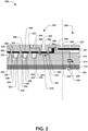
- Fig. 2 illustrates a cross-sectional view of an apparatus 200 comprising an RC snubber 201 integrated into a unipolar power transistor of the apparatus 200.
- the apparatus 200 comprises an active trench transistor cell region 202 within which one or more unipolar power transistors are located. In an embodiment, a source 244 of a unipolar power transistor is located within the active trench transistor cell region 202.
- the apparatus 200 comprises a gate pad area 204 within which a gate pad of a gate 207 of the apparatus 200 is formed.
- the apparatus 200 comprises a semiconductor substrate 212.
- the semiconductor substrate 212 comprises a silicon carbide substrate.
- the silicon carbide substrate is an n+ silicon carbide substrate.
- the semiconductor substrate 212 comprises a gallium nitride substrate. It may be appreciated that the semiconductor substrate 212 may comprise other materials.
- the apparatus 200 comprises a first layer 214.
- the first layer 214 is a drift zone layer, such as an n- drift zone layer.
- the first layer 214 is positioned over the semiconductor substrate 212 of the apparatus 200.
- the first layer 214 is an n-doped drift zone comprising n type material.
- the first layer 214 is an n type layer forming part of a capacitor 220 of the RC snubber 201.
- the apparatus 200 comprises a second layer 210.
- the second layer 210 is an anode layer, such as a p+ type anode layer.
- the second layer 210 is connected to the source 244.
- the second layer 210 is positioned over the first layer 214 of the apparatus 200.
- the second layer 210 is a p type layer forming a part of the capacitor 220 of the RC snubber 201. In this way, the first layer 214 as the n type layer and the second layer 210 as the p type layer form a p-n junction of the capacitor 220 of the RC snubber 201.
- the p-n junction protects a drain 242 of the unipolar power transistor of the apparatus 200.
- the apparatus 200 comprises a third layer 222.
- the third layer 222 is a gate oxide layer.
- the third layer 222 comprises a gate oxide material, such as a silicon dioxide material, a high-k material, a dielectric material, etc.
- the third layer 222 is positioned over the second layer 210.
- the apparatus 200 comprises a poly silicon structure 221, such as an s-poly plate.
- the poly silicon structure 221 is positioned over the third layer 222 such as over the gate oxide layer.
- the poly silicon structure 221 is positioned within the gate pad area 204.
- the poly silicon structure 221 is used to separate the drain 242 of the unipolar power transistor from the gate 207 of the unipolar power transistor.
- the gate 207 comprises a conductive material.
- the conductive material comprises aluminum copper AlCu or other metal or conductive material.
- the poly silicon structure 221 is connected to a source snubber potential (Ssn) (e.g., a portion of the source structure 206 positioned over the poly silicon structure 221 and the resistor 218).
- Ssn source snubber potential
- the apparatus 200 comprises an inter layer dielectric (ILD) layer 208.
- the ILD layer 208 comprises a low-k dielectric material, such as a material having a k-value (dielectric constant) lower than about 3.9.
- Some low-k dielectric materials have a k-value lower than about 3.5 and may have a k-value lower than about 2.5.
- Some examples of low-k dielectric materials are SiOxCyHz, SiOx, SiCN, oxygen doped SiC (ODC), nitrogen doped SiC (NDC), chemical vapor deposition (CVD) from tetraethyl orthosilicate (TEOS), or other suitable material, where x, y, and z are integers greater than or equal to 1.
- a portion of the ILD layer 208 within the gate pad area 204 is positioned between the gate 207 of the unipolar power transistor and the poly silicon structure 221. In an embodiment, other portions of the ILD layer 208 within the active trench transistor cell region 202 are positioned over poly silicon trench gate structures 224 within the active trench transistor cell region 202.
- the poly silicon trench gate structures 224 within the active trench transistor cell region 202 are positioned between the ILD layer 208 and the third layer 222 (e.g., the gate oxide layer), such as where the ILD layer 208 is positioned adjacent to a top side of a poly silicon trench gate structure 224 and the third layer 222 (e.g., the gate oxide layer) is positioned adjacent to one or more of a bottom side, a first side, and/or a second side of the poly silicon trench gate structure 224.
- the third layer 222 e.g., the gate oxide layer
- the apparatus 200 comprises the source structure 206.
- the source structure 206 comprises the source 244 of the unipolar power transistor.
- the source structure 206 comprises a conductive material.
- the conductive material comprise aluminum copper AlCu or other metal or conductive material.
- a first dimension (e.g., a height) of the source structure is between about 3 ⁇ m and about 7 ⁇ m, such as about 5 ⁇ m or any other size.
- a portion of the source structure 206 within the active trench transistor cell region 202 is positioned over the poly silicon trench gate structures 224.
- another portion of the source structure 206 such as the source snubber potential (Ssn) is positioned between the source 244 of the unipolar power transistor and the gate 207 of the unipolar power transistor.
- the apparatus 200 comprises contact metal structures 232.
- the contact metal structures 232 are positioned within the active trench transistor cell region 202.
- the contact metal structures 232 are positioned between portions of the ILD layer 208 that are overlaying the poly silicon trench gate structures 224 within the active trench transistor cell region 202.
- the apparatus 200 comprises source material structures 230.
- the source material structures 230 comprises n+ source material.
- the source material structures 230 are positioned below one or more contact metal structures 232 within the active trench transistor cell region 202.
- the apparatus 200 comprises body structures 228.
- the body structures 228 comprise p- material.
- the body structures 228 are positioned below the source material structures 230 within the active trench transistor cell region 202.
- the apparatus 200 comprises structures 226.
- the structures 226 comprise n- type material.
- the structures 226 are positioned below the body structures 228 within the active trench transistor cell region 202.
- the source material structures 230, the body structures 228, and the structures 226 form npn structures.
- An npn structure is used as a channel for the unipolar power transistor through which current can flow.
- the apparatus 200 comprises the RC snubber 201 that is integrated into and is formed as part of the apparatus 200 and the unipolar power transistor.
- the RC snubber 201 and the unipolar transistor are coupled in parallel.
- the RC snubber 201 and the unipolar power transistor are monolithically formed on the semiconductor substrate 212. That is, the RC snubber 201 and the unipolar power transistor are formed on the same semiconductor substrate 212.
- the RC snubber 201 comprises a resistor 218 and the capacitor 220.
- the resistor 218 is comprised of n+ material 216, such as n+ material 216 connected to the source 244 of the unipolar power transistor (e.g., connected to a portion of the source structure 206 positioned over the resistor 218).
- the resistor 218 is formed from an n type source doping bridge within the unipolar power transistor.
- the resistor 218 has a resistance between about 500k ⁇ and about 1.5k ⁇ , such as about 1k ⁇ or any other resistance.
- the n+ material 216 may have a resistance between about 400 ⁇ /sq and about 800 ⁇ /sq, such as 600 ⁇ /sq or any other resistance.
- the resistor 218 has a length between about 15 ⁇ m and about 25 ⁇ m, such as about 20 ⁇ m or any other length. In an embodiment, the resistor 218 has a width between about 8 ⁇ m and about 16 ⁇ m, such as about 12 ⁇ m or any other width. In an embodiment, the resistance of the resistor 218 and a capacitance Coss of the capacitor 220 (e.g., 20pF, 50pF, etc.) can be adapted by using different widths and lengths for the resistor 218.
- a capacitance Coss of the capacitor 220 e.g., 20pF, 50pF, etc.
- the resistor 218 is positioned below the source 244 of the unipolar power transistor, such as below the source structure 206. In an embodiment, the resistor 218 is positioned below a portion of the ILD layer 208. A portion of the third layer 222 (e.g., the gate oxide layer) may be positioned between the portion of the ILD layer 208 and the resistor 218. The resistor 218 may be positioned over the second layer 210. In an embodiment, the resistor 218 is the result of a dopant implant. In an embodiment, the resistor 218 is formed by n type material (e.g., a n+ implant) that is used as a source region for the unipolar power transistor.
- n type material e.g., a n+ implant
- n type material of the unipolar power transistor is also used for the resistor 218, and also poly material of the unipolar power transistor (e.g., the poly silicon structure 221) is also used to form the RC snubber 201, and thus the RC snubber 201 is integrated into the apparatus 200 as part of the unipolar power transistor.
- the RC snubber 201 can be formed without additional layers and components within the apparatus 200.
- the capacitor 220 is positioned between the poly silicon structure 221 and the semiconductor substrate 212.
- the capacitor 220 comprises a p-n junction.
- the p-n junction comprises p type material of the second layer 210 (e.g., the anode layer).
- the p-n junction comprises n type material of the first layer 214 (e.g., the drift zone layer).
- the p-n junction is used to protect the drain 242 of the unipolar power transistor.
- the capacitor 220 is electrically connected to the resistor 218.
- the resistor 218 and the capacitor 220 of the RC snubber 201 are integrated into the apparatus 200 and the unipolar power transistor in order to dampen oscillations associated with the unipolar power transistor being switched between states, which would otherwise cause electromagnetic interference adversely affecting the operation of the apparatus 200.
- Fig. 3 illustrates a top down view 300 of the apparatus 200.
- the resistor 218 is formed from the n+ material 216.
- the resistor 218 is positioned over the second layer 210.
- the resistor 218 is positioned over the contact metal structures 232.
- the resistor 218 has a length 302 between about 15 ⁇ m and about 25 ⁇ m, such as about 20 ⁇ m or any other length.
- the resistor 218 has a width 304 between about 8 ⁇ m and about 16 ⁇ m, such as about 12 ⁇ m or any other width.
- the length 302 and the width 304 may be design parameters that may be sized according to various criteria, such as sized to provide a particular resistance for the RC snubber 201, such as to achieve a resistance of about 1K ⁇ .
- the top down view 300 also illustrates the gate 207, portions of the ILD layer 208, and the first layer 214 (e.g., the drift zone layer).
- Fig. 4 illustrates a top down view 400 of certain layers (e.g., some layers are visible for illustrative purposes, while other layers, such as the ILD layer 208 and the poly silicon structure 221, are not visible so that the substrate 212 is visible) of the apparatus 200 configured with a snubber layer.
- the snubber layer comprises the RC snubber 201 integrated into the apparatus 200 and the unipolar power transistor.
- the RC snubber layer also comprises a plurality of resistors, as opposed to the single resistor 218 illustrated by Figs. 2 and 3 .
- the plurality of resistors comprise a first resistor 402, a second resistor 404, a third resistor 406, and a fourth resistor 408.
- the number of resistors of the plurality of resistors may comprise any number of resistors, and that 4 resistors are illustrated merely as an example.
- the first resistor 402, the second resistor 404, the third resistor 406, and the fourth resistor 408 are distributed around the gate 207 of the unipolar power transistor.
- the first resistor 402, the second resistor 404, the third resistor 406, and the fourth resistor 408 are shunted in parallel.
- the first resistor 402, the second resistor 404, the third resistor 406, and the fourth resistor 408 are resistance regions that connect source snubber potential (Ssn) (e.g., a portion of the source structure 206 positioned over the resistor 218) to the source 244 of the unipolar power transistor.
- the top down view 400 also illustrates a layer through a void 410 (e.g., as illustrated in Fig. 2 , an opening in the ILD layer 208 through which the source structure 206 contacts the poly silicon structure 221 (e.g., through which the connection between the resistor 218 and the capacitor 220 passes)) and the second layer 210.
- the RC snubber 201 of the apparatus 200 provides improved dampening of oscillations without using additional components (e.g., components external to the unipolar power transistor) since the RC snubber 201 is integrated into the apparatus 200 and the unipolar power transistor (e.g., a resistor and capacitor of the RC snubber 201 are formed from portions of the unipolar power transistor). Because the RC snubber 201 is incorporated into the apparatus 200 and the unipolar power transistor, such as within an area under the gate 207 (a gate pad) that is already part of the apparatus 200, little to no additional area is consumed by the RC snubber 201.
- additional components e.g., components external to the unipolar power transistor
- the RC snubber 201 provides dissipation of power loss in the RC snubber 201 because the apparatus 200 is well cooled.
- the RC snubber 201 can work directly against oscillation to dampen the oscillation because there is no parasitic inductance involved.
- the RC snubber 201 scales with the number of parallel apparatuses/transistors in a module because RC snubbers are integrated into each apparatus/transistor. Because the RC snubber 201 is integrated with the unipolar power transistor as opposed to being external to the unipolar power transistor, leak inductance otherwise occurring between external RC snubber and the unipolar power transistor are reduced or eliminated.
- the RC snubber 201 also softens the switching behavior of the unipolar power transistor.
- An embodiment of the presently disclosed subject matter comprises an apparatus.
- the apparatus comprises a unipolar power transistor; and an RC snubber comprising: a capacitor between a poly silicon structure and a semiconductor substrate, wherein the capacitor comprises a p-n junction; and a resistor between a source of the unipolar power transistor and a first layer forming the capacitor; wherein the unipolar power transistor and the RC snubber are coupled in parallel, and wherein the RC snubber and the unipolar power transistor are formed monolithically on the semiconductor substrate.
- the semiconductor substrate comprises a silicon carbide substrate.
- the p-n junction comprises p type material of the first layer and n type material of a second layer.
- the second layer is between the first layer and the semiconductor substrate.
- the resistor is formed from an n type source doping bridge within the unipolar power transistor.
- the poly silicon structure is connected to the source.
- the poly silicon structure separates a drain of the unipolar power transistor from a gate of the unipolar power transistor.
- the resistor comprises an n type material layer connected to the source.
- the resistor is electrically coupled to the capacitor.
- the first layer comprises a p type material.
- the unipolar power transistor comprises a 3 terminal transistor.
- the unipolar power transistor comprises at least one of a silicon carbide metal-oxide-semiconductor field-effect transistor (MOSFET) or a silicon carbide junction gate field-effect transistor (JFET).
- MOSFET silicon carbide metal-oxide-semiconductor field-effect transistor
- JFET silicon carbide junction gate field-effect transistor
- the capacitor is located at an output side of the unipolar power transistor.
- the semiconductor substrate comprises a gallium nitride substrate.
- the apparatus comprises an RC snubber layer comprising: the RC snubber, and a plurality of resistors, wherein the plurality of resistors comprises the resistor.
- the terms “component,” “module,” “system”, “interface”, and the like are generally intended to refer to a computer-related entity, either hardware, a combination of hardware and software, software, or software in execution.
- One or more components may be localized on one computer and/or distributed between two or more computers.
- the claimed subject matter may be implemented as a method, apparatus, or article of manufacture using standard programming and/or engineering techniques to produce software, firmware, hardware, or any combination thereof to control a computer to implement the disclosed subject matter.
- article of manufacture as used herein is intended to encompass a computer program accessible from any computer-readable device, carrier, or media.
- one or more of the operations described may constitute computer readable instructions stored on one or more computer readable media, which if executed by a computing device, will cause the computing device to perform the operations described.
- the order in which some or all of the operations are described should not be construed as to imply that these operations are necessarily order dependent. Alternative ordering will be appreciated by one skilled in the art having the benefit of this description. Further, it will be understood that not all operations are necessarily present in each embodiment provided herein.
- any aspect or design described herein as an "example” is not necessarily to be construed as advantageous over other aspects or designs. Rather, use of the word “example” is intended to present one possible aspect and/or implementation that may pertain to the techniques presented herein. Such examples are not necessary for such techniques or intended to be limiting. Various embodiments of such techniques may include such an example, alone or in combination with other features, and/or may vary and/or omit the illustrated example.
- first,” “second,” or the like are not intended to imply a temporal aspect, a spatial aspect, an ordering, etc. Rather, such terms are merely used as identifiers, names, etc. for features, elements, items, etc.
- a first element and a second element generally correspond to element A and element B or two different or two identical elements or the same element.
Landscapes
- Metal-Oxide And Bipolar Metal-Oxide Semiconductor Integrated Circuits (AREA)
- Semiconductor Integrated Circuits (AREA)
- Engineering & Computer Science (AREA)
- Power Engineering (AREA)
Abstract
Description
- The present disclosure relates to the field of dampening oscillations within semiconductor devices.
- Various types of transistors, such as silicon carbide metal-oxide-semiconductor field-effect transistors (SiC MOSFETS) and other types of transistors, may be used for applications in high power and high voltage range use, such as in traction and wind energy applications. These types of applications may utilize high currents and large power modules or parallel connection modules. Operation of these transistors may result in relatively high commutation inductances, such as in the range of 20nH - 100nH per commutation path. If a load current in one of these transistors is switched off quickly, commutation oscillations may be triggered. The commutation oscillations can result in electromagnetic interference and/or failure to comply with electromagnetic interference limits. Such commutation oscillations are undesirable for applications that utilize high load currents.
- This Summary is provided to introduce a selection of concepts in a simplified form that are further described below in the Detailed Description. This Summary is not intended to identify key factors or essential features of the claimed subject matter, nor is it intended to be used to limit the scope of the claimed subject matter.
- In an embodiment of the techniques presented herein, an apparatus is provided. The apparatus comprises a unipolar power transistor. The apparatus comprises an RC snubber coupled in parallel within the unipolar power transistor. The RC snubber and the unipolar power transistor are formed monolithically on a semiconductor substrate. The RC snubber comprises a capacitor. The capacitor is between a poly silicon structure and the semiconductor substrate. The capacitor comprises a p-n junction. The RC snubber comprises a resistor. The resistor is between a source of the unipolar power transistor and a first layer forming the capacitor.
- To the accomplishment of the foregoing and related ends, the following description and annexed drawings set forth certain illustrative aspects and implementations. These are indicative of but a few of the various ways in which one or more aspects may be employed. Other aspects, advantages, and novel features of the disclosure will become apparent from the following detailed description when considered in conjunction with the annexed drawings.
-
-
Fig. 1 is a component block diagram illustrating an apparatus comprising a half-bridge including two transistors each one coupled in parallel with an RC snubber formed on a same semiconductor substrate. -
Fig. 2 is a cross section of an apparatus comprising a transistor coupled in parallel with an RC snubber formed on a same semiconductor substrate. -
Fig. 3 is a top down view of an apparatus comprising a transistor coupled in parallel with an RC snubber formed on a same semiconductor substrate. -
Fig. 4 is a top down view of an apparatus configured with a snubber layer. - The claimed subject matter is now described with reference to the drawings, wherein like reference numerals are used to refer to like elements throughout. In the following description, for purposes of explanation, numerous specific details are set forth in order to provide a thorough understanding of the claimed subject matter. It may be evident, however, that the claimed subject matter may be practiced without these specific details. In other instances, well-known structures and devices are shown in block diagram form in order to facilitate describing the claimed subject matter.
- Within the field of electronics, transistors such as silicon carbide metal-oxide-semiconductor field-effect transistors (SiC MOSFETS), silicon carbide junction gate field-effect transistors (SiC JFET), unipolar power transistors, etc., may be used for various applications, such as for switching in high powered and/or high voltage applications. When a transistor of a device is being switched, commutation oscillations can be triggered, thus causing undesirable oscillation energy within the device that can negatively affect operation of the device. For example, the commutation oscillations may be triggered when the transistor is used as a power transistor with high voltages (e.g., voltages over 600 volts) such that switching off the transistor is so rapid that commutation oscillations result. These commutation oscillations can be high-frequency LC oscillations that negatively affect operation of the device. For example, the commutation oscillations can result in electromagnetic interference that impact the correct operation of the device. In an example of electromagnetic interference, a transistor may be initially in an off state. While in the on state, a drain and source voltage of the transistor is low. When the transistor is switched off, voltage starts to increase until reaching a DC voltage. Current starts to decrease during a normal operation mode, and thus oscillations will start to occur. The oscillations will cause unwanted electromagnetic interference.
- One technique for dampening commutation oscillations in a device relates to using insulated-gate bipolar transistor (IGBT) components or unipolar components such as SiC MOSFETs that can be operated with high gate resistances. However, this can result in increased switching losses that negatively affect the overall efficiency of the device. Another technique that can be used to help dampen commutation oscillations in a device relates to the use of an RC network/snubber. An RC snubber can be used for power electronics to react to high-frequency LC oscillations in order to dampen such oscillations. With the oscillations, a capacitor of the RC snubber causes current through a resistor in order to dampen the oscillations, which also results in a loss that could be unacceptable. These RC snubbers are external to the transistors that are being dampened, such as being placed on a load connection or on auxiliary connections. This causes leakage inductance (parasitic inductance) between the RC snubber and the transistor (the chip).
- Accordingly, as provided herein, an RC snubber is integrated into an apparatus for damping oscillations of a unipolar power transistor of the apparatus. The RC snubber and the unipolar power transistor are coupled together in parallel. The RC snubber and the unipolar power transistor are formed monolithically on the same semiconductor substrate, and thus the RC snubber and the unipolar power transistor are integrated together within the same semiconductor device, such as where a resistor and a capacitor of the RC snubber are formed from layers of materials making up the unipolar power transistor, and thus the RC snubber is formed as part of the unipolar power transistor. Because the RC snubber is integrated into the apparatus and is formed on the same semiconductor substrate as the unipolar power transistor, the RC snubber can be positioned closer to (as part of) the unipolar power transistor than if the RC snubber was external to the unipolar power transistor. This provides improved damping of oscillations while reducing leakage inductance otherwise resulting from the RC snubber being external to the apparatus and unipolar power transistor. Because the RC snubber is integrated into the unipolar power transistor, less area within the apparatus is consumed by the RC snubber. Integration of the RC snubber into the unipolar power transistor allows for scaling out for devices that comprise a large number of unipolar power transistors since each unipolar power transistor has its own integrated RC snubber.
- The disclosed RC snubber provides various advantages over external RC snubbers and other techniques used to dampen oscillations, such as oscillations in applications with high Lxl products, where an Lxl product corresponds to a product of a commutation inductance (e.g.,
inductance 102 ofFig. 1 ) and current flowing therethrough. With this RC snubber, there is no additional/external component being used as the RC snubber since the RC snubber is integrated into the apparatus and the unipolar power transistor. Because the RC snubber is incorporated within the unipolar power transistor, such as within an area under a gate pad that is already part of the apparatus, little to no additional area is consumed by the RC snubber. The RC snubber provides dissipation of power loss in the RC snubber because the apparatus is well cooled. The RC snubber can work directly against oscillation to dampen the oscillation because there is no parasitic inductance involved. The RC snubber scales with the number of parallel apparatuses/transistors in a module because the RC snubbers are integrated into each apparatus/transistor. -
Fig. 1 illustrates anapparatus including module 100 comprisingRC snubbers 110. The apparatus further comprises aDC link capacitor 104. The DC link capacitor may be used as an intermediate circuit capacitor that provides a low impedance path for switching currents and provides energy storage. Themodule 100 may be connected to aload 120. Themodule 100 comprises afirst body diode 108. In an embodiment, themodule 100 comprises a first unipolar power transistor, and thefirst body diode 108 is between a drain and a source of the first unipolar power transistor. Thefirst body diode 108 is formed by a p-n junction of the first unipolar power transistor between the source and the drain of the first unipolar power transistor. Themodule 100 may comprise any number of unipolar power transistors, such as a second unipolar power transistor that has asecond body diode 106 between a drain and a source of the second unipolar power transistor. Thesecond body diode 106 is formed by a p-n junction of the second unipolar power transistor between the source and the drain of the second unipolar power transistor. The unipolar transistors ofmodule 100 selectivelycouple load 120 to either aDC link potential 122 or toground 124. DC link potential may be 600V, 1200V, 1800V or even 3.3kV or higher in some embodiments.Ground 124 may be 0V or even below 0V in some embodiments. Themodule 100 has aninductance 102, such as a parasitic inductance corresponding to the inductance of a connection between theDC link capacitor 104 and themodule 100. - In an embodiment, the first unipolar power transistor and/or the second unipolar power transistor are SiC MOSFET transistors. In an embodiment, the first unipolar power transistor and/or the second unipolar power transistor are SiC JFET transistors. In an embodiment, the first unipolar power transistor and/or the second unipolar power transistor are 3 terminal transistors because the RC snubbers are integrated into the unipolar power transistors without the need of additional terminals to connect to external RC snubbers.
- The
module 100 may comprise any number ofRC snubbers 110, such as afirst RC snubber 111 integrated into and coupled with the first unipolar power transistor in parallel and asecond RC snubber 113 integrated into and coupled within the second unipolar power transistor in parallel. Thefirst RC snubber 111 and the first unipolar power transistor are formed monolithically on a first semiconductor substrate. In an embodiment, the first semiconductor substrate comprises a silicon carbide substrate. In an embodiment, the first semiconductor substrate comprises a gallium nitride substrate. Thesecond RC snubber 113 and the second unipolar power transistor are formed monolithically on a second semiconductor substrate. In an embodiment, the second semiconductor substrate comprises a silicon carbide substrate. In an embodiment, the second semiconductor substrate comprises a gallium nitride substrate. - The
first RC snubber 111 comprises afirst capacitor 114 and afirst resistor 112. Thefirst capacitor 114 is located between a poly silicon structure of the first unipolar power transistor and the first semiconductor substrate. The poly silicon structure may be connected to the source of the first unipolar power transistor. The poly silicon structure separates a drain of the first unipolar power transistor from a gate of the first unipolar power transistor. Thefirst capacitor 114 comprises a p-n junction, such as the p-n junction of the first unipolar power transistor that forms thefirst body diode 108. The p-n junction may comprise a first layer comprising p type material and a second layer comprising n type material. The second layer is between the first layer and the second semiconductor substrate. Thefirst capacitor 114 is located at an output side of the first unipolar power transistor. Thefirst resistor 112 is located between a source of the first unipolar power transistor and the first layer forming thefirst capacitor 114. In an embodiment, thefirst resistor 112 comprises an n type material connected to the source of the first unipolar power transistor. In an embodiment, thefirst resistor 112 is formed from an n type source doping bridge within the first unipolar power transistor. In an embodiment, thefirst resistor 112 and thefirst capacitor 114 are electrically coupled to one another. - The
second RC snubber 113 comprises asecond capacitor 118 and asecond resistor 116. Thesecond capacitor 118 is located between a poly silicon structure of the second unipolar power transistor and the second semiconductor substrate. The poly silicon structure may be connected to the source of the second unipolar power transistor. The poly silicon structure separates a drain of the second unipolar power transistor from a gate of the second unipolar power transistor. Thesecond capacitor 118 comprises a p-n junction, such as the p-n junction of the second unipolar power transistor that forms thesecond body diode 106. The p-n junction may comprise a first layer comprising p type material and a second layer comprising n type material. The second layer is between the first layer and the second semiconductor substrate. Thesecond capacitor 118 is located at an output side of the second unipolar power transistor. Thesecond resistor 116 is located between a source of the second unipolar power transistor and the first layer forming thesecond capacitor 118. In an embodiment, thesecond resistor 116 comprises an n type material connected to the source of the second unipolar power transistor. In an embodiment, thesecond resistor 116 is formed from an n type source doping bridge within the first unipolar power transistor. In an embodiment, thesecond resistor 116 and thesecond capacitor 118 are electrically coupled to one another. - In an embodiment, the
module 100 may comprise an RC snubber layer. The RC snubber layer may comprise an RC snubber used to dampen oscillations within a unipolar power transistor. The RC snubber layer may comprise a plurality of resistors. In order to distribute losses from the RC snubber, the resistors may be implemented as resistance bridges positioned around one or more sides of a gate pad of the unipolar power transistor in order to distribute the resistance, and thus distribute the losses from the RC snubber dampening the oscillations. - It may be appreciated that an embodiment of an RC snubber that is integrated into a unipolar power transistor is further described in conjunction with
Figs. 2 ― 4. -
Fig. 2 illustrates a cross-sectional view of anapparatus 200 comprising anRC snubber 201 integrated into a unipolar power transistor of theapparatus 200. Theapparatus 200 comprises an active trenchtransistor cell region 202 within which one or more unipolar power transistors are located. In an embodiment, asource 244 of a unipolar power transistor is located within the active trenchtransistor cell region 202. Theapparatus 200 comprises agate pad area 204 within which a gate pad of agate 207 of theapparatus 200 is formed. Theapparatus 200 comprises asemiconductor substrate 212. In an embodiment, thesemiconductor substrate 212 comprises a silicon carbide substrate. In an embodiment, the silicon carbide substrate is an n+ silicon carbide substrate. In an embodiment, thesemiconductor substrate 212 comprises a gallium nitride substrate. It may be appreciated that thesemiconductor substrate 212 may comprise other materials. - The
apparatus 200 comprises afirst layer 214. In an embodiment, thefirst layer 214 is a drift zone layer, such as an n- drift zone layer. In an embodiment, thefirst layer 214 is positioned over thesemiconductor substrate 212 of theapparatus 200. In an embodiment, thefirst layer 214 is an n-doped drift zone comprising n type material. In an embodiment, thefirst layer 214 is an n type layer forming part of acapacitor 220 of theRC snubber 201. - The
apparatus 200 comprises asecond layer 210. In an embodiment, thesecond layer 210 is an anode layer, such as a p+ type anode layer. In an embodiment, thesecond layer 210 is connected to thesource 244. In an embodiment, thesecond layer 210 is positioned over thefirst layer 214 of theapparatus 200. In an embodiment, thesecond layer 210 is a p type layer forming a part of thecapacitor 220 of theRC snubber 201. In this way, thefirst layer 214 as the n type layer and thesecond layer 210 as the p type layer form a p-n junction of thecapacitor 220 of theRC snubber 201. The p-n junction protects adrain 242 of the unipolar power transistor of theapparatus 200. - The
apparatus 200 comprises athird layer 222. In an embodiment, thethird layer 222 is a gate oxide layer. In an embodiment, thethird layer 222 comprises a gate oxide material, such as a silicon dioxide material, a high-k material, a dielectric material, etc. In an embodiment, thethird layer 222 is positioned over thesecond layer 210. - The
apparatus 200 comprises apoly silicon structure 221, such as an s-poly plate. In an embodiment, thepoly silicon structure 221 is positioned over thethird layer 222 such as over the gate oxide layer. In an embodiment, thepoly silicon structure 221 is positioned within thegate pad area 204. In an embodiment, thepoly silicon structure 221 is used to separate thedrain 242 of the unipolar power transistor from thegate 207 of the unipolar power transistor. In an embodiment, thegate 207 comprises a conductive material. In an embodiment, the conductive material comprises aluminum copper AlCu or other metal or conductive material. In an embodiment, thepoly silicon structure 221 is connected to a source snubber potential (Ssn) (e.g., a portion of thesource structure 206 positioned over thepoly silicon structure 221 and the resistor 218). - The
apparatus 200 comprises an inter layer dielectric (ILD)layer 208. In an embodiment, theILD layer 208 comprises a low-k dielectric material, such as a material having a k-value (dielectric constant) lower than about 3.9. Some low-k dielectric materials have a k-value lower than about 3.5 and may have a k-value lower than about 2.5. Some examples of low-k dielectric materials are SiOxCyHz, SiOx, SiCN, oxygen doped SiC (ODC), nitrogen doped SiC (NDC), chemical vapor deposition (CVD) from tetraethyl orthosilicate (TEOS), or other suitable material, where x, y, and z are integers greater than or equal to 1. In an embodiment, a portion of theILD layer 208 within thegate pad area 204 is positioned between thegate 207 of the unipolar power transistor and thepoly silicon structure 221. In an embodiment, other portions of theILD layer 208 within the active trenchtransistor cell region 202 are positioned over poly silicontrench gate structures 224 within the active trenchtransistor cell region 202. In an embodiment, the poly silicontrench gate structures 224 within the active trenchtransistor cell region 202 are positioned between theILD layer 208 and the third layer 222 (e.g., the gate oxide layer), such as where theILD layer 208 is positioned adjacent to a top side of a poly silicontrench gate structure 224 and the third layer 222 (e.g., the gate oxide layer) is positioned adjacent to one or more of a bottom side, a first side, and/or a second side of the poly silicontrench gate structure 224. - The
apparatus 200 comprises thesource structure 206. In an embodiment, thesource structure 206 comprises thesource 244 of the unipolar power transistor. In an embodiment, thesource structure 206 comprises a conductive material. In an embodiment, the conductive material comprise aluminum copper AlCu or other metal or conductive material. In an embodiment, a first dimension (e.g., a height) of the source structure is between about 3µm and about 7µm, such as about 5µm or any other size. In an embodiment, a portion of thesource structure 206 within the active trenchtransistor cell region 202 is positioned over the poly silicontrench gate structures 224. In an embodiment, another portion of thesource structure 206, such as the source snubber potential (Ssn), is positioned between thesource 244 of the unipolar power transistor and thegate 207 of the unipolar power transistor. - The
apparatus 200 comprisescontact metal structures 232. In an embodiment, thecontact metal structures 232 are positioned within the active trenchtransistor cell region 202. In an embodiment, thecontact metal structures 232 are positioned between portions of theILD layer 208 that are overlaying the poly silicontrench gate structures 224 within the active trenchtransistor cell region 202. - The
apparatus 200 comprises sourcematerial structures 230. In an embodiment, the sourcematerial structures 230 comprises n+ source material. In an embodiment, the sourcematerial structures 230 are positioned below one or morecontact metal structures 232 within the active trenchtransistor cell region 202. - The
apparatus 200 comprisesbody structures 228. In an embodiment, thebody structures 228 comprise p- material. In an embodiment, thebody structures 228 are positioned below the sourcematerial structures 230 within the active trenchtransistor cell region 202. - The
apparatus 200 comprisesstructures 226. In an embodiment, thestructures 226 comprise n- type material. In an embodiment, thestructures 226 are positioned below thebody structures 228 within the active trenchtransistor cell region 202. - In an embodiment, the source
material structures 230, thebody structures 228, and thestructures 226 form npn structures. An npn structure is used as a channel for the unipolar power transistor through which current can flow. - The
apparatus 200 comprises theRC snubber 201 that is integrated into and is formed as part of theapparatus 200 and the unipolar power transistor. TheRC snubber 201 and the unipolar transistor are coupled in parallel. In particular, theRC snubber 201 and the unipolar power transistor are monolithically formed on thesemiconductor substrate 212. That is, theRC snubber 201 and the unipolar power transistor are formed on thesame semiconductor substrate 212. TheRC snubber 201 comprises aresistor 218 and thecapacitor 220. In an embodiment, theresistor 218 is comprised ofn+ material 216, such asn+ material 216 connected to thesource 244 of the unipolar power transistor (e.g., connected to a portion of thesource structure 206 positioned over the resistor 218). In an embodiment, theresistor 218 is formed from an n type source doping bridge within the unipolar power transistor. In an embodiment, theresistor 218 has a resistance between about 500kΩ and about 1.5kΩ, such as about 1kΩ or any other resistance. In an embodiment, then+ material 216 may have a resistance between about 400Ω/sq and about 800Ω/sq, such as 600 Ω/sq or any other resistance. In an embodiment, theresistor 218 has a length between about 15µm and about 25µm, such as about 20µm or any other length. In an embodiment, theresistor 218 has a width between about 8µm and about 16µm, such as about 12µm or any other width. In an embodiment, the resistance of theresistor 218 and a capacitance Coss of the capacitor 220 (e.g., 20pF, 50pF, etc.) can be adapted by using different widths and lengths for theresistor 218. - In an embodiment, the
resistor 218 is positioned below thesource 244 of the unipolar power transistor, such as below thesource structure 206. In an embodiment, theresistor 218 is positioned below a portion of theILD layer 208. A portion of the third layer 222 (e.g., the gate oxide layer) may be positioned between the portion of theILD layer 208 and theresistor 218. Theresistor 218 may be positioned over thesecond layer 210. In an embodiment, theresistor 218 is the result of a dopant implant. In an embodiment, theresistor 218 is formed by n type material (e.g., a n+ implant) that is used as a source region for the unipolar power transistor. In this way, n type material of the unipolar power transistor is also used for theresistor 218, and also poly material of the unipolar power transistor (e.g., the poly silicon structure 221) is also used to form theRC snubber 201, and thus theRC snubber 201 is integrated into theapparatus 200 as part of the unipolar power transistor. Thus, theRC snubber 201 can be formed without additional layers and components within theapparatus 200. - The
capacitor 220 is positioned between thepoly silicon structure 221 and thesemiconductor substrate 212. In an embodiment, thecapacitor 220 comprises a p-n junction. The p-n junction comprises p type material of the second layer 210 (e.g., the anode layer). The p-n junction comprises n type material of the first layer 214 (e.g., the drift zone layer). The p-n junction is used to protect thedrain 242 of the unipolar power transistor. Thecapacitor 220 is electrically connected to theresistor 218. In this way, theresistor 218 and thecapacitor 220 of theRC snubber 201 are integrated into theapparatus 200 and the unipolar power transistor in order to dampen oscillations associated with the unipolar power transistor being switched between states, which would otherwise cause electromagnetic interference adversely affecting the operation of theapparatus 200. -
Fig. 3 illustrates a top downview 300 of theapparatus 200. Theresistor 218 is formed from then+ material 216. Theresistor 218 is positioned over thesecond layer 210. Theresistor 218 is positioned over thecontact metal structures 232. Theresistor 218 has alength 302 between about 15µm and about 25µm, such as about 20µm or any other length. Theresistor 218 has awidth 304 between about 8µm and about 16µm, such as about 12µm or any other width. Thelength 302 and thewidth 304 may be design parameters that may be sized according to various criteria, such as sized to provide a particular resistance for theRC snubber 201, such as to achieve a resistance of about 1KΩ. The top downview 300 also illustrates thegate 207, portions of theILD layer 208, and the first layer 214 (e.g., the drift zone layer). -
Fig. 4 illustrates a top downview 400 of certain layers (e.g., some layers are visible for illustrative purposes, while other layers, such as theILD layer 208 and thepoly silicon structure 221, are not visible so that thesubstrate 212 is visible) of theapparatus 200 configured with a snubber layer. The snubber layer comprises theRC snubber 201 integrated into theapparatus 200 and the unipolar power transistor. The RC snubber layer also comprises a plurality of resistors, as opposed to thesingle resistor 218 illustrated byFigs. 2 and3 . The plurality of resistors comprise afirst resistor 402, asecond resistor 404, athird resistor 406, and afourth resistor 408. It may be appreciated that the number of resistors of the plurality of resistors may comprise any number of resistors, and that 4 resistors are illustrated merely as an example. Thefirst resistor 402, thesecond resistor 404, thethird resistor 406, and thefourth resistor 408 are distributed around thegate 207 of the unipolar power transistor. In an embodiment, thefirst resistor 402, thesecond resistor 404, thethird resistor 406, and thefourth resistor 408 are shunted in parallel. In an embodiment, thefirst resistor 402, thesecond resistor 404, thethird resistor 406, and thefourth resistor 408 are resistance regions that connect source snubber potential (Ssn) (e.g., a portion of thesource structure 206 positioned over the resistor 218) to thesource 244 of the unipolar power transistor. The top downview 400 also illustrates a layer through a void 410 (e.g., as illustrated inFig. 2 , an opening in theILD layer 208 through which thesource structure 206 contacts the poly silicon structure 221 (e.g., through which the connection between theresistor 218 and thecapacitor 220 passes)) and thesecond layer 210. - The
RC snubber 201 of theapparatus 200 provides improved dampening of oscillations without using additional components (e.g., components external to the unipolar power transistor) since theRC snubber 201 is integrated into theapparatus 200 and the unipolar power transistor (e.g., a resistor and capacitor of theRC snubber 201 are formed from portions of the unipolar power transistor). Because theRC snubber 201 is incorporated into theapparatus 200 and the unipolar power transistor, such as within an area under the gate 207 (a gate pad) that is already part of theapparatus 200, little to no additional area is consumed by theRC snubber 201. TheRC snubber 201 provides dissipation of power loss in theRC snubber 201 because theapparatus 200 is well cooled. TheRC snubber 201 can work directly against oscillation to dampen the oscillation because there is no parasitic inductance involved. TheRC snubber 201 scales with the number of parallel apparatuses/transistors in a module because RC snubbers are integrated into each apparatus/transistor. Because theRC snubber 201 is integrated with the unipolar power transistor as opposed to being external to the unipolar power transistor, leak inductance otherwise occurring between external RC snubber and the unipolar power transistor are reduced or eliminated. TheRC snubber 201 also softens the switching behavior of the unipolar power transistor. - An embodiment of the presently disclosed subject matter comprises an apparatus. The apparatus comprises a unipolar power transistor; and an RC snubber comprising: a capacitor between a poly silicon structure and a semiconductor substrate, wherein the capacitor comprises a p-n junction; and a resistor between a source of the unipolar power transistor and a first layer forming the capacitor; wherein the unipolar power transistor and the RC snubber are coupled in parallel, and wherein the RC snubber and the unipolar power transistor are formed monolithically on the semiconductor substrate.
- According to some embodiments, the semiconductor substrate comprises a silicon carbide substrate.
- According to some embodiments, the p-n junction comprises p type material of the first layer and n type material of a second layer.
- According to some embodiments, the second layer is between the first layer and the semiconductor substrate.
- According to some embodiments, the resistor is formed from an n type source doping bridge within the unipolar power transistor.
- According to some embodiments, the poly silicon structure is connected to the source.
- According to some embodiments, the poly silicon structure separates a drain of the unipolar power transistor from a gate of the unipolar power transistor.
- According to some embodiments, the resistor comprises an n type material layer connected to the source.
- According to some embodiments, the resistor is electrically coupled to the capacitor.
- According to some embodiments, the first layer comprises a p type material.
- According to some embodiments, the unipolar power transistor comprises a 3 terminal transistor.
- According to some embodiments, the unipolar power transistor comprises at least one of a silicon carbide metal-oxide-semiconductor field-effect transistor (MOSFET) or a silicon carbide junction gate field-effect transistor (JFET).
- According to some embodiments, the capacitor is located at an output side of the unipolar power transistor.
- According to some embodiments, the semiconductor substrate comprises a gallium nitride substrate.
- According to some embodiments, the apparatus comprises an RC snubber layer comprising: the RC snubber, and a plurality of resistors, wherein the plurality of resistors comprises the resistor.
- Although the subject matter has been described in language specific to structural features and/or methodological acts, it is to be understood that the subject matter defined in the appended claims is not necessarily limited to the specific features or acts described above. Rather, the specific features and acts described above are disclosed as example forms of implementing the claims.
- As used in this application, the terms "component," "module," "system", "interface", and the like are generally intended to refer to a computer-related entity, either hardware, a combination of hardware and software, software, or software in execution. One or more components may be localized on one computer and/or distributed between two or more computers.
- Furthermore, the claimed subject matter may be implemented as a method, apparatus, or article of manufacture using standard programming and/or engineering techniques to produce software, firmware, hardware, or any combination thereof to control a computer to implement the disclosed subject matter. The term "article of manufacture" as used herein is intended to encompass a computer program accessible from any computer-readable device, carrier, or media. Of course, those skilled in the art will recognize many modifications may be made to this configuration without departing from the scope or spirit of the claimed subject matter.
- Various operations of embodiments are provided herein. In one embodiment, one or more of the operations described may constitute computer readable instructions stored on one or more computer readable media, which if executed by a computing device, will cause the computing device to perform the operations described. The order in which some or all of the operations are described should not be construed as to imply that these operations are necessarily order dependent. Alternative ordering will be appreciated by one skilled in the art having the benefit of this description. Further, it will be understood that not all operations are necessarily present in each embodiment provided herein.
- Any aspect or design described herein as an "example" is not necessarily to be construed as advantageous over other aspects or designs. Rather, use of the word "example" is intended to present one possible aspect and/or implementation that may pertain to the techniques presented herein. Such examples are not necessary for such techniques or intended to be limiting. Various embodiments of such techniques may include such an example, alone or in combination with other features, and/or may vary and/or omit the illustrated example.
- As used in this application, the term "or" is intended to mean an inclusive "or" rather than an exclusive "or". That is, unless specified otherwise, or clear from context, "X employs A or B" is intended to mean any of the natural inclusive permutations. That is, if X employs A; X employs B; or X employs both A and B, then "X employs A or B" is satisfied under any of the foregoing instances. In addition, the articles "a" and "an" as used in this application and the appended claims may generally be construed to mean "one or more" unless specified otherwise or clear from context to be directed to a singular form. Also, unless specified otherwise, "first," "second," or the like are not intended to imply a temporal aspect, a spatial aspect, an ordering, etc. Rather, such terms are merely used as identifiers, names, etc. for features, elements, items, etc. For example, a first element and a second element generally correspond to element A and element B or two different or two identical elements or the same element.
- Also, although the disclosure has been shown and described with respect to one or more implementations, equivalent alterations and modifications will occur to others skilled in the art based upon a reading and understanding of this specification and the annexed drawings. The disclosure includes all such modifications and alterations and is limited only by the scope of the following claims. In particular regard to the various functions performed by the above described components (e.g., elements, resources, etc.), the terms used to describe such components are intended to correspond, unless otherwise indicated, to any component which performs the specified function of the described component (e.g., that is functionally equivalent), even though not structurally equivalent to the disclosed structure which performs the function in the herein illustrated example implementations of the disclosure. In addition, while a particular feature of the disclosure may have been disclosed with respect to only one of several implementations, such feature may be combined with one or more other features of the other implementations as may be desired and advantageous for any given or particular application. Furthermore, to the extent that the terms "includes", "having", "has", "with", or variants thereof are used in either the detailed description or the claims, such terms are intended to be inclusive in a manner similar to the term "comprising."
Claims (15)
- An apparatus (200), comprising:a unipolar power transistor; andan RC snubber (201) comprising:a capacitor (220) between a poly silicon structure (221) and a semiconductor substrate (212), wherein the capacitor comprises a p-n junction; anda resistor (218) between a source (244) of the unipolar power transistor and a first layer (214) forming the capacitor (220);wherein the unipolar power transistor and the RC snubber (201) are coupled in parallel, andwherein the RC snubber (201) and the unipolar power transistor are formed monolithically on the semiconductor substrate (212).
- The apparatus (200) of claim 1, wherein the semiconductor substrate (212) comprises a silicon carbide substrate.
- The apparatus (200) of any one of the preceding claims, wherein the p-n junction comprises p type material of the first layer (212) and n type material of a second layer (214).
- The apparatus (200) of claim 3, wherein the second layer (214) is between the first layer (212) and the semiconductor substrate (212).
- The apparatus (200) of any one of the preceding claims, wherein the resistor (218) is formed from an n type source doping bridge within the unipolar power transistor.
- The apparatus (200) of any one of the preceding claims, wherein the poly silicon structure (221) is connected to the source (244).
- The apparatus (200) of any one of the preceding claims, wherein the poly silicon structure (221) separates a drain (242) of the unipolar power transistor from a gate (207) of the unipolar power transistor.
- The apparatus (200) of any one of the preceding claims, wherein the resistor (218) comprises an n type material layer connected to the source (244).
- The apparatus (200) of any one of the preceding claims, wherein the resistor (218) is electrically coupled to the capacitor (220).
- The apparatus (200) of any one of the preceding claims, wherein the first layer (212) comprises a p type material.
- The apparatus (200) of any one of the preceding claims, wherein the unipolar power transistor comprises a three-terminal transistor.
- The apparatus (200) of any one of the preceding claims, wherein the unipolar power transistor comprises at least one of a silicon carbide metal-oxide-semiconductor field-effect transistor - MOSFET - or a silicon carbide junction gate field-effect transistor - JFET.
- The apparatus (200) of any one of the preceding claims, wherein the capacitor (220) is located at an output side of the unipolar power transistor.
- The apparatus (200) of any one of the preceding claims, wherein the semiconductor substrate (212) comprises a gallium nitride substrate.
- The apparatus (200) of any one of the preceding claims, comprising:
an RC snubber layer comprising:the RC snubber, anda plurality of resistors, wherein the plurality of resistors comprises the resistor.
Applications Claiming Priority (1)
| Application Number | Priority Date | Filing Date | Title |
|---|---|---|---|
| US17/019,746 US11563322B2 (en) | 2020-09-14 | 2020-09-14 | RC snubber |
Publications (1)
| Publication Number | Publication Date |
|---|---|
| EP3968389A1 true EP3968389A1 (en) | 2022-03-16 |
Family
ID=77626897
Family Applications (1)
| Application Number | Title | Priority Date | Filing Date |
|---|---|---|---|
| EP21020444.2A Pending EP3968389A1 (en) | 2020-09-14 | 2021-09-02 | Unipolar power transistor and rc snubber |
Country Status (3)
| Country | Link |
|---|---|
| US (1) | US11563322B2 (en) |
| EP (1) | EP3968389A1 (en) |
| CN (1) | CN114188417A (en) |
Cited By (1)
| Publication number | Priority date | Publication date | Assignee | Title |
|---|---|---|---|---|
| CN115996572A (en) * | 2023-03-24 | 2023-04-21 | 长鑫存储技术有限公司 | Semiconductor device and semiconductor memory |
Families Citing this family (1)
| Publication number | Priority date | Publication date | Assignee | Title |
|---|---|---|---|---|
| US12278231B2 (en) * | 2022-03-11 | 2025-04-15 | Infineon Technologies Ag | RC snubber with poly silicon resistor and capacitor formed from junction termination edge |
Citations (4)
| Publication number | Priority date | Publication date | Assignee | Title |
|---|---|---|---|---|
| US20090242977A1 (en) * | 2008-03-28 | 2009-10-01 | Kabushiki Kaisha Toshiba | Semiconductor device and dc-dc converter |
| US20120049263A1 (en) * | 2010-08-30 | 2012-03-01 | Wei-Chieh Lin | Semiconductor device having extra capacitor structure and manufacturing method thereof |
| US20140264477A1 (en) * | 2013-03-15 | 2014-09-18 | United Silicon Carbide, Inc. | Vjfet devices |
| US20170263747A1 (en) * | 2016-03-11 | 2017-09-14 | Kabushiki Kaisha Toshiba | Semiconductor device |
Family Cites Families (1)
| Publication number | Priority date | Publication date | Assignee | Title |
|---|---|---|---|---|
| US10593664B2 (en) * | 2016-12-27 | 2020-03-17 | Infineon Technologies Americas Corp. | Controlled resistance integrated snubber for power switching device |
-
2020
- 2020-09-14 US US17/019,746 patent/US11563322B2/en active Active
-
2021
- 2021-09-02 EP EP21020444.2A patent/EP3968389A1/en active Pending
- 2021-09-10 CN CN202111062008.7A patent/CN114188417A/en active Pending
Patent Citations (4)
| Publication number | Priority date | Publication date | Assignee | Title |
|---|---|---|---|---|
| US20090242977A1 (en) * | 2008-03-28 | 2009-10-01 | Kabushiki Kaisha Toshiba | Semiconductor device and dc-dc converter |
| US20120049263A1 (en) * | 2010-08-30 | 2012-03-01 | Wei-Chieh Lin | Semiconductor device having extra capacitor structure and manufacturing method thereof |
| US20140264477A1 (en) * | 2013-03-15 | 2014-09-18 | United Silicon Carbide, Inc. | Vjfet devices |
| US20170263747A1 (en) * | 2016-03-11 | 2017-09-14 | Kabushiki Kaisha Toshiba | Semiconductor device |
Cited By (2)
| Publication number | Priority date | Publication date | Assignee | Title |
|---|---|---|---|---|
| CN115996572A (en) * | 2023-03-24 | 2023-04-21 | 长鑫存储技术有限公司 | Semiconductor device and semiconductor memory |
| CN115996572B (en) * | 2023-03-24 | 2023-07-25 | 长鑫存储技术有限公司 | Semiconductor device and semiconductor memory |
Also Published As
| Publication number | Publication date |
|---|---|
| US20220085601A1 (en) | 2022-03-17 |
| US11563322B2 (en) | 2023-01-24 |
| CN114188417A (en) | 2022-03-15 |
Similar Documents
| Publication | Publication Date | Title |
|---|---|---|
| US11217577B2 (en) | Controlled resistance integrated snubber for power switching device | |
| US9209292B2 (en) | Charge compensation semiconductor devices | |
| CN106024854B (en) | Semiconductor device and method for manufacturing the same | |
| TW202109771A (en) | A power semiconductor device with an auxiliary gate structure | |
| US20090242977A1 (en) | Semiconductor device and dc-dc converter | |
| US6388280B2 (en) | Semiconductor device | |
| US11588048B2 (en) | Semiconductor device with insulated gate transistor cell and rectifying junction | |
| US11563322B2 (en) | RC snubber | |
| US20210134968A1 (en) | Semiconductor Device and Inverter | |
| JP2017126690A (en) | Semiconductor device | |
| JP2022543376A (en) | silicon carbide transistor device | |
| US6404041B1 (en) | EMC-optimized power switch | |
| KR102824851B1 (en) | Voltage-controlled switching device with resistive path | |
| JP2004281462A (en) | Power semiconductor device | |
| EP4243062A1 (en) | Rc snubber with poly silicon resistor and capacitor formed from junction termination edge | |
| US20230418319A1 (en) | Semiconductor transistors having minimum gate-to-source voltage clamp circuits | |
| US12074226B2 (en) | Schottky diode integrated with a semiconductor device | |
| KR20230073111A (en) | Semiconductor device | |
| EP3817066A1 (en) | Semiconductor devices | |
| US12549103B2 (en) | Power transistors with resonant clamping circuits | |
| US20250294865A1 (en) | Semiconductor devices having intrinsic gate-to-drain capacitances that are only partly in series with a gate resistor | |
| US20240429915A1 (en) | Asymmetric power module | |
| KR20250146525A (en) | Power semiconductor device and power semiconductor chip | |
| KR20250146529A (en) | Power semiconductor device and power semiconductor chip | |
| KR20230119146A (en) | Termination structure with reduced dynamic output capacitance loss |
Legal Events
| Date | Code | Title | Description |
|---|---|---|---|
| PUAI | Public reference made under article 153(3) epc to a published international application that has entered the european phase |
Free format text: ORIGINAL CODE: 0009012 |
|
| STAA | Information on the status of an ep patent application or granted ep patent |
Free format text: STATUS: THE APPLICATION HAS BEEN PUBLISHED |
|
| AK | Designated contracting states |
Kind code of ref document: A1 Designated state(s): AL AT BE BG CH CY CZ DE DK EE ES FI FR GB GR HR HU IE IS IT LI LT LU LV MC MK MT NL NO PL PT RO RS SE SI SK SM TR |
|
| STAA | Information on the status of an ep patent application or granted ep patent |
Free format text: STATUS: REQUEST FOR EXAMINATION WAS MADE |
|
| 17P | Request for examination filed |
Effective date: 20220906 |
|
| RBV | Designated contracting states (corrected) |
Designated state(s): AL AT BE BG CH CY CZ DE DK EE ES FI FR GB GR HR HU IE IS IT LI LT LU LV MC MK MT NL NO PL PT RO RS SE SI SK SM TR |