EP3968371A1 - Semiconductor structure and manufacturing method therefor - Google Patents
Semiconductor structure and manufacturing method therefor Download PDFInfo
- Publication number
- EP3968371A1 EP3968371A1 EP20896064.1A EP20896064A EP3968371A1 EP 3968371 A1 EP3968371 A1 EP 3968371A1 EP 20896064 A EP20896064 A EP 20896064A EP 3968371 A1 EP3968371 A1 EP 3968371A1
- Authority
- EP
- European Patent Office
- Prior art keywords
- groove
- inclined plane
- semiconductor structure
- present disclosure
- substrate
- Prior art date
- Legal status (The legal status is an assumption and is not a legal conclusion. Google has not performed a legal analysis and makes no representation as to the accuracy of the status listed.)
- Granted
Links
Images



Classifications
-
- H—ELECTRICITY
- H10—SEMICONDUCTOR DEVICES; ELECTRIC SOLID-STATE DEVICES NOT OTHERWISE PROVIDED FOR
- H10W—GENERIC PACKAGES, INTERCONNECTIONS, CONNECTORS OR OTHER CONSTRUCTIONAL DETAILS OF DEVICES COVERED BY CLASS H10
- H10W20/00—Interconnections in chips, wafers or substrates
- H10W20/40—Interconnections external to wafers or substrates, e.g. back-end-of-line [BEOL] metallisations or vias connecting to gate electrodes
- H10W20/41—Interconnections external to wafers or substrates, e.g. back-end-of-line [BEOL] metallisations or vias connecting to gate electrodes characterised by their conductive parts
- H10W20/435—Cross-sectional shapes or dispositions of interconnections
-
- H—ELECTRICITY
- H10—SEMICONDUCTOR DEVICES; ELECTRIC SOLID-STATE DEVICES NOT OTHERWISE PROVIDED FOR
- H10W—GENERIC PACKAGES, INTERCONNECTIONS, CONNECTORS OR OTHER CONSTRUCTIONAL DETAILS OF DEVICES COVERED BY CLASS H10
- H10W20/00—Interconnections in chips, wafers or substrates
- H10W20/01—Manufacture or treatment
- H10W20/031—Manufacture or treatment of conductive parts of the interconnections
- H10W20/069—Manufacture or treatment of conductive parts of the interconnections by forming self-aligned vias or self-aligned contact plugs
-
- H—ELECTRICITY
- H10—SEMICONDUCTOR DEVICES; ELECTRIC SOLID-STATE DEVICES NOT OTHERWISE PROVIDED FOR
- H10B—ELECTRONIC MEMORY DEVICES
- H10B12/00—Dynamic random access memory [DRAM] devices
- H10B12/01—Manufacture or treatment
- H10B12/02—Manufacture or treatment for one transistor one-capacitor [1T-1C] memory cells
- H10B12/03—Making the capacitor or connections thereto
- H10B12/033—Making the capacitor or connections thereto the capacitor extending over the transistor
- H10B12/0335—Making a connection between the transistor and the capacitor, e.g. plug
-
- H—ELECTRICITY
- H10—SEMICONDUCTOR DEVICES; ELECTRIC SOLID-STATE DEVICES NOT OTHERWISE PROVIDED FOR
- H10B—ELECTRONIC MEMORY DEVICES
- H10B12/00—Dynamic random access memory [DRAM] devices
- H10B12/30—DRAM devices comprising one-transistor - one-capacitor [1T-1C] memory cells
-
- H—ELECTRICITY
- H10—SEMICONDUCTOR DEVICES; ELECTRIC SOLID-STATE DEVICES NOT OTHERWISE PROVIDED FOR
- H10B—ELECTRONIC MEMORY DEVICES
- H10B12/00—Dynamic random access memory [DRAM] devices
- H10B12/30—DRAM devices comprising one-transistor - one-capacitor [1T-1C] memory cells
- H10B12/31—DRAM devices comprising one-transistor - one-capacitor [1T-1C] memory cells having a storage electrode stacked over the transistor
- H10B12/315—DRAM devices comprising one-transistor - one-capacitor [1T-1C] memory cells having a storage electrode stacked over the transistor with the capacitor higher than a bit line
-
- H—ELECTRICITY
- H10—SEMICONDUCTOR DEVICES; ELECTRIC SOLID-STATE DEVICES NOT OTHERWISE PROVIDED FOR
- H10D—INORGANIC ELECTRIC SEMICONDUCTOR DEVICES
- H10D64/00—Electrodes of devices having potential barriers
- H10D64/01—Manufacture or treatment
- H10D64/011—Manufacture or treatment of electrodes ohmically coupled to a semiconductor
- H10D64/0111—Manufacture or treatment of electrodes ohmically coupled to a semiconductor to Group IV semiconductors
- H10D64/0113—Manufacture or treatment of electrodes ohmically coupled to a semiconductor to Group IV semiconductors the conductive layers comprising highly doped semiconductor materials, e.g. polysilicon layers or amorphous silicon layers
-
- H—ELECTRICITY
- H10—SEMICONDUCTOR DEVICES; ELECTRIC SOLID-STATE DEVICES NOT OTHERWISE PROVIDED FOR
- H10W—GENERIC PACKAGES, INTERCONNECTIONS, CONNECTORS OR OTHER CONSTRUCTIONAL DETAILS OF DEVICES COVERED BY CLASS H10
- H10W20/00—Interconnections in chips, wafers or substrates
- H10W20/01—Manufacture or treatment
- H10W20/031—Manufacture or treatment of conductive parts of the interconnections
- H10W20/056—Manufacture or treatment of conductive parts of the interconnections by filling conductive material into holes, grooves or trenches
- H10W20/057—Manufacture or treatment of conductive parts of the interconnections by filling conductive material into holes, grooves or trenches by selectively depositing, e.g. by using selective CVD or plating
-
- H—ELECTRICITY
- H10—SEMICONDUCTOR DEVICES; ELECTRIC SOLID-STATE DEVICES NOT OTHERWISE PROVIDED FOR
- H10W—GENERIC PACKAGES, INTERCONNECTIONS, CONNECTORS OR OTHER CONSTRUCTIONAL DETAILS OF DEVICES COVERED BY CLASS H10
- H10W20/00—Interconnections in chips, wafers or substrates
- H10W20/01—Manufacture or treatment
- H10W20/031—Manufacture or treatment of conductive parts of the interconnections
- H10W20/056—Manufacture or treatment of conductive parts of the interconnections by filling conductive material into holes, grooves or trenches
- H10W20/059—Manufacture or treatment of conductive parts of the interconnections by filling conductive material into holes, grooves or trenches by reflowing or applying pressure
-
- H—ELECTRICITY
- H10—SEMICONDUCTOR DEVICES; ELECTRIC SOLID-STATE DEVICES NOT OTHERWISE PROVIDED FOR
- H10W—GENERIC PACKAGES, INTERCONNECTIONS, CONNECTORS OR OTHER CONSTRUCTIONAL DETAILS OF DEVICES COVERED BY CLASS H10
- H10W20/00—Interconnections in chips, wafers or substrates
- H10W20/01—Manufacture or treatment
- H10W20/031—Manufacture or treatment of conductive parts of the interconnections
- H10W20/069—Manufacture or treatment of conductive parts of the interconnections by forming self-aligned vias or self-aligned contact plugs
- H10W20/0696—Manufacture or treatment of conductive parts of the interconnections by forming self-aligned vias or self-aligned contact plugs by using sacrificial placeholders, e.g. using sacrificial plugs
-
- H—ELECTRICITY
- H10—SEMICONDUCTOR DEVICES; ELECTRIC SOLID-STATE DEVICES NOT OTHERWISE PROVIDED FOR
- H10W—GENERIC PACKAGES, INTERCONNECTIONS, CONNECTORS OR OTHER CONSTRUCTIONAL DETAILS OF DEVICES COVERED BY CLASS H10
- H10W20/00—Interconnections in chips, wafers or substrates
- H10W20/01—Manufacture or treatment
- H10W20/071—Manufacture or treatment of dielectric parts thereof
- H10W20/081—Manufacture or treatment of dielectric parts thereof by forming openings in the dielectric parts
- H10W20/083—Manufacture or treatment of dielectric parts thereof by forming openings in the dielectric parts the openings being via holes penetrating underlying conductors
-
- H—ELECTRICITY
- H10—SEMICONDUCTOR DEVICES; ELECTRIC SOLID-STATE DEVICES NOT OTHERWISE PROVIDED FOR
- H10W—GENERIC PACKAGES, INTERCONNECTIONS, CONNECTORS OR OTHER CONSTRUCTIONAL DETAILS OF DEVICES COVERED BY CLASS H10
- H10W20/00—Interconnections in chips, wafers or substrates
- H10W20/40—Interconnections external to wafers or substrates, e.g. back-end-of-line [BEOL] metallisations or vias connecting to gate electrodes
- H10W20/41—Interconnections external to wafers or substrates, e.g. back-end-of-line [BEOL] metallisations or vias connecting to gate electrodes characterised by their conductive parts
- H10W20/44—Conductive materials thereof
- H10W20/4451—Semiconductor materials, e.g. polysilicon
Definitions
- the present disclosure relates to the field of semiconductor fabrication technologies, and more particularly, to a semiconductor structure that can avoid forming air gaps and a fabrication method thereof.
- a storage node contact (SNC) structure is a contact structure for connecting transistors and storage capacitors in a DRAM structure.
- the SNC is a polycrystalline silicon.
- a bottom of the SNC is connected to a substrate and a shallow trench isolation (STI) structure, a top thereof is connected to metal, and sidewalls thereof are sidewalls of the isolation structure.
- the isolation structure is, for example, a bit line structure or a dielectric layer structure.
- the bit line structure is fabricated in advance, and thus it is required to fabricate the dielectric layer structure as the isolation structure to fabricate the other two sidewalls of the SNC trench, and the polycrystalline silicon is filled into the trench to fabricate the SNC. Due to larger hardness, the sidewalls of the dielectric layer can only be fabricated by deposition. As a result, the trench between the sidewalls of the dielectric layer formed by deposition is generally a trapezoidal structure (with reference to FIG. 3 of the specification), which is narrow at the top and wide at the bottom. Therefore, it is difficult to control uniformity of the deposition in the deposition process of the polycrystalline silicon, such that air gaps may be easily formed inside the SNC, which causes changes of electrical properties of the SNC, leads to component failure, and reduces the yield.
- An objective of the present disclosure is to provide a semiconductor structure and a fabrication method thereof, to overcome, at least to a certain extent, the problem of forming air gaps inside a polycrystalline silicon in the process of fabricating an SNC structure due to limitations of related technologies.
- a semiconductor structure including:
- a top area of the groove is smaller than a bottom area of the groove.
- an inclination angle of the first inclined plane ranges from 30° to 40°.
- a bottom of the groove further has a second inclined plane, and the second inclined plane is formed on the shallow trench isolation region.
- an inclination angle of the second inclined plane ranges from 20° to 60°.
- the plurality of isolation structures include bit line structures and dielectric layer structures.
- shapes of cross sections of the plurality of grooves include one or more of a square, a polygon, a circle, or an ellipse.
- the plurality of grooves are arranged in an array.
- the first inclined plane is a cambered surface.
- a method for fabricating a semiconductor structure including:
- an inclination angle of the first inclined plane ranges from 30° to 40°.
- the first inclined plane is subjected to natural oxide removal treatment and/or carbon-based residue removal treatment.
- the etching down an exposed part of the active region at a bottom of the second groove to form a first inclined plane further includes: simultaneously etching an exposed part of the shallow trench isolation structure adjacent to the exposed part of the active region to form a second inclined plane.
- an etching selectivity of the exposed part of the active region with respect to an etching selectivity of the exposed part of the shallow trench isolation structure is 1:1.
- the inclined planes are etched using sulfur hexafluoride gas.
- the performing an epitaxial silicon growth process in the second groove includes: setting a flow rate of hydrochloric acid as 150sccm ⁇ 30%.
- the performing an epitaxial silicon growth process in the second groove includes: after filling the second groove, removing a polycrystalline silicon by using a wet process to remain only a monocrystalline silicon, and trimming a top of filled silicon to be a flat plane.
- the method further includes: depositing metal on a surface of the filled silicon.
- an inclined plane is arranged in the exposed part of the active region at the bottom of the groove containing the SNC structure, and the polycrystalline silicon is grown inside the groove by taking the inclined plane as a substrate.
- the SNC structure containing no air gap can be quickly formed, a component failure rate can be reduced, and a yield rate can be enhanced.
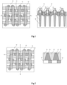
- FIG. 1 illustrates a schematic diagram of an arrangement mode of an SNC structure according to an exemplary embodiment of the present disclosure.
- the structure on the right side of FIG. 1 is a cross-sectional view along Position A-A of the structure as shown on the left side of FIG. 1 .
- the Position A-A is perpendicular to a bit line (BL) and parallel to a word line (WL).
- a storage node contact (SNC) structure 11 is located between sidewalls of two bit line structures 12 at corresponding positions in two adjacent rows of word lines, and a bottom of the SNC structure 11 is connected to an active region 14 and a shallow trench isolation (STI) structure 13.
- STI shallow trench isolation
- FIG. 2 illustrates a schematic diagram of another arrangement mode of the SNC structure according to an exemplary embodiment of the present disclosure.
- the structure on the right side of FIG. 2 is a cross-sectional view along Position B-B of the structure as shown on the left side of FIG. 2 .
- the Position B-B is perpendicular to the word line (WL) and is parallel to the bit line (BL).
- the adjacent SNC structures are isolated by isolation structures 15, the isolation structures 15 include dielectric layer structures.
- the storage node contact (SNC) structure 11 in FIG. 2 is still connected, at the bottom thereof, to the active region 14 and the shallow trench isolation structure 13.
- cross-sectional positions are different, such that proportions of the active region 14 and the shallow trench isolation structure 13 in the cross section are different.
- the present disclosure for the sake of simplicity, only the regional positions and proportions as shown in FIG. 2 are employed, but the present disclosure is not limited thereto.
- FIG. 3 illustrates a schematic diagram of a fabrication process of the SNC structure in the related technologies.
- the isolation structures between the SNC structures include bit line structures and dielectric layer sidewalls, and thus it is required to form the dielectric layer sidewalls when fabricating a groove for containing the SNC structures.
- the dielectric layer sidewalls are difficult to be formed by etching. Therefore, in the related technologies, generally a trench is fabricated (as shown in Step a) by etching a sacrificial layer material 31 (which is generally an oxide, such as silicon dioxide, BPSG, BSG, and so on) in the Direction B-B as shown in FIG. 2 , and dielectric layer structures 15 are fabricated (as shown in Step b) by using a deposition technology.
- a sacrificial layer material 31 which is generally an oxide, such as silicon dioxide, BPSG, BSG, and so on
- Step d the remaining sacrificial layer material 31 is removed (as shown in Step c), and a polycrystalline silicon is deposited between the dielectric layer structures 15 to fabricate the SNC structure 11 (as shown in Step d).
- isolation structures such as the isolation structures 12 on the right side of FIG. 1
- the isolation structures including the bit line structures generally are formed before the dielectric layer structures 15 are formed.
- the cross-section of the remaining sacrificial layer material is a trapezoid.
- the SNC structure finally fabricated is also a trapezoidal cross section which is narrow at the top and wide at the bottom, making it difficult to complete good deposition of the polycrystalline silicon, which often forms air gaps in the SNC structure (as shown in Step d).
- the embodiments of the present disclosure provide a semiconductor structure capable of avoiding forming the air gaps in the SNC structure.
- FIG. 4 illustrates a schematic diagram of a semiconductor structure according to an embodiment of the present disclosure.
- FIG. 4 is a cross-sectional view along the Position B-B of the structure as shown on the left side of FIG. 2 , and there exists isolation structures (such as the isolation structures 12 on the right side of FIG. 1 ) including the bit line structures in the front and rear of the viewing direction in the figures.
- the semiconductor structure 400 may include:
- FIG. 4 is a cross-sectional view in the Direction B-B in FIG. 2 , the isolation structures 15 marked in FIG. 4 actually are dielectric layer structures, i.e., the isolation structures 15 on the right side of FIG. 2 .
- the isolation structures 15 in the embodiments of the present disclosure further include the bit line structures 12 as shown in FIG. 1 , and the bit line structures 12 are in the front or rear of the viewing direction in FIG. 4 . That is, the isolation structures 15 in the embodiments of the present disclosure include four sidewall structures such as two adjacent bit line structures and two adjacent dielectric layer structures, to realize encirclement and isolation of the groove 42.
- a top area of the groove 42 is smaller than a bottom area thereof, and cross-sectional shapes of the plurality of grooves include one or more of a square, a polygon, a circle, or an ellipse.
- the plurality of grooves 42 are arranged in an array, wherein the array may be an aligned or staggered dot array. It is to be understood that two opposite sidewalls of the groove 42 are formed by the isolation structures including the bit line structures, and the bit line structure is perpendicular to the substrate. Therefore, a length of a top surface of the groove 42 may be equal to that of a bottom surface thereof, or a width of the top surface of the groove 42 may be equal to that of the bottom surface, which is not particularly limited in the present disclosure.
- an inclination angle of the first inclined plane 43 may be 30°-40°, for example.
- a slope of the other region is different from that of the first inclined plane, which may be, for example, a horizontal region (for example, a bottom shape of the SNC structure 11 in the structure on the right side of FIG. 1 ).
- the first inclined plane 43 may also be a cambered surface formed in an etching process, which is not particularly limited in the present disclosure.
- FIG. 5 illustrates a flowchart of a method for fabricating the semiconductor structure as shown in FIG. 4 .
- the method 500 for fabricating the semiconductor structure may include:
- the sacrificial layer is, for example, an oxide layer, including but not limited to materials such as oxide (such as silicon dioxide), BPSG, BSG, and the like.
- the first groove is, for example, an inverted trapezoidal groove which is wide at the top and narrow at the bottom
- the second groove is, for example, a trapezoidal groove which is narrow at the bottom and wide at the top.
- a non-inverted trapezoidal first groove may also be formed here, wherein a shape of the first groove is determined by factors such as technology means and technological conditions; and the second groove may also be a non-trapezoidal groove, wherein a shape of the second groove is related to the shape of the first groove.
- FIG. 6A to FIG. 6D illustrate schematic diagrams of the process of the steps as shown in FIG. 5 .
- FIG. 6A to FIG. 6D are merely for the purpose of illustration, and are not intended to limit the positions and proportions of the active regions and the shallow trench isolation regions in the actual processes.
- the first groove 45 is also etched on the sacrificial layer 44 to make preparations for the subsequent fabrication of the isolation structure.
- the active region 14 and the shallow trench isolation region 13 are exposed at the bottom of the first groove 45 at the same time.
- the bit line structures in the front or rear of the viewing direction of the figures generally have already been formed. Therefore, the step as shown in FIG. 6A actually refers to filling the sacrificial layer between the bit line structures and then etching the first groove 45 in the sacrificial layer. That is, two sidewalls in the front and rear of the viewing direction of the first groove 45 are perpendicular to each other and are formed by the isolation structures including the bit line structures.
- the isolation structures 15 are fabricated in the same way by depositing a dielectric layer, wherein a material of the dielectric layer is, for example, silicon nitride.
- Step (c) in FIG. 3 space is created for the fabrication of the SNC also by removing the sacrificial layer 44 to form the second groove 42, and the active region 14 and the shallow trench isolation region 13 are exposed at the bottom of the second groove 42 at the same time.
- the cross-sectional positions are different (that is, the Line B-B moves transversely)
- the proportions of the active region and the shallow trench isolation region exposed at the bottom of the second groove 42 actually are different. Therefore, although the embodiments of the present disclosure merely show one type of exposed state of the active region and the shallow trench isolation region, in practical applications, the active region and the shallow trench isolation region may have many types of exposed states.
- the SNC is fabricated by means of an epitaxial silicon growth process. Therefore, for the smooth progress of the epitaxial silicon growth process, the bottom of the second groove 42 is processed. That is, the first inclined plane 43 is fabricated at the bottom of the second groove 42 through a dry etching process or wet etching process, etc.
- both the active region and the shallow trench isolation region are exposed at the bottom of the second groove 42 (referring to the structure on the left side of FIG. 2 ).
- the material of the active region generally is monocrystalline silicon
- the material of the shallow trench isolation region generally is oxide (for example, silicon dioxide).
- the active region and the shallow trench isolation region provide completely different environments for the growth of the epitaxial silicon.
- the monocrystalline silicon generally grows only on one side of the monocrystalline silicon, and the monocrystalline silicon is hard to grow or grows at a slow rate on one side of the silicon dioxide. Therefore, to provide more crystal orientations for the growth of the monocrystalline silicon and to ensure the growth of the monocrystalline silicon more uniform and more rapid, in the embodiments of the present disclosure, the first inclined plane 43 is fabricated before the epitaxial silicon growth process.
- gas for etching the first inclined plane 43 may be, for example, sulfur hexafluoride (SF6).
- the first inclined plane 43 whose inclination angle is 30°-40° may be etched by controlling parameters such as bias and flow of the etching gas. It is to be noted that in the etching process, generally it is unable to ensure that a perfect plane is etched. Therefore, in the actual fabrication processes, the first inclined plane 43 may also be a cambered surface formed by the etching process, wherein the shape of the cambered surface may be as shown in FIG. 7A .
- the active region also likely has other regions such as planes. That is, an end point of the first inclined plane 43 formed by etching does not coincide with an edge of the active region. In this case, the state of the active region may be as shown in FIG. 7B .
- an etching selectivity may be controlled to be, for example, 1:1 to form the second inclined plane 46.
- the inclination angle of the second inclined plane 46 is, for example, 20°-60°.
- the second inclined plane 46 may also be a cambered surface, or the edge of the second inclined plane 46 does not coincide with the edge of the shallow trench isolation region. Reference may be made to FIG. 7A and FIG. 7B respectively for these two states.
- the inclined plane at the bottom of the second groove 42 is actually similar to a bowl shape placed upright. There exists an inclined plane at the bottom of the second groove 42 no matter it is viewed from the cross section in the Direction A-A in FIG. 1 or it is viewed from the cross section in the Direction B-B in FIG. 2 .
- FIG. 8A and FIG. 8B viewed from the cross section in the Direction A-A on the left side of FIG. 1 , the active region 14 and the shallow trench isolation region 13 may have different proportions and different inclined planes.
- the first inclined plane 43 also may be cleaned in situ by means of dry cleaning of oxides or dry cleaning of removing carbon-based residues, etc., to ensure the purity of the monocrystalline silicon interface, so as to obtain high-quality growth effects.
- the monocrystalline silicon may grow taking the inclined plane as the substrate until the epitaxial silicon is controlled to fill the entire second groove 42 up to form the conductive plug 11 as shown in FIG. 4 .
- the conductive plug 11 is a storage node contact (SNC) structure.
- SNC storage node contact
- a growth selectivity of the polycrystalline silicon may be reduced in step S4, and a growth rate of that may be increased.
- the growth selectivity may be reduced by setting an appropriate flow of hydrochloric acid.
- the concentration of the hydrochloric acid is, for example, 150 sccm ⁇ 30%.
- Increase of the flow of the hydrochloric acid may inhibit the growth of polycrystals and tend to grow on the surface of a monocrystal.
- Decrease of the flow of the hydrochloric acid may increase the growth rate of the polycrystalline silicon and increase the yield. Therefore, it is required to seek the most appropriate flow range of the hydrochloric acid to ensure the quality of the monocrystal and to increase the yield. Therefore, the above range is set in the embodiments of the present disclosure.
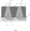
- the monocrystalline silicon and the polycrystalline silicon may grow at the same time, and thus their shapes are not easy to control, as shown in FIG. 9A or FIG. 9B .
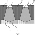
- the polycrystalline silicon may be removed by means of recess etch such as a wet process to only leave the monocrystal silicon, and the shape of the top of the monocrystalline silicon may be trimmed to a plane roughly (as shown in FIG. 10 ), and the length of the conductive plug is adjusted for the subsequent metal connection process.
- the conductive plug is a storage node contact.
- a capacitive landing pad made of a metal material may be formed on the storage node contact for subsequent fabrication of a capacitor on the interface platform.
- the connection of the landing pad made of the metal material onto the storage node contact belongs to the fabrication of a metal-semiconductor contact structure. Therefore, in another embodiment of the present disclosure, after filling the second groove, metal may be deposited on the surface of the conductive plug 11.
- the above-mentioned landing pad is in contact with the monocrystalline silicon, which is a case where metal is in contact with the monocrystalline silicon, similar to the case of contact between a source and a drain of a transistor in a peripheral circuit.
- a metallization process is implemented, and optimal process conditions may be achieved at the same time, which makes process condition requirements simpler, improves the performance of the contact structure, and allows a contact resistance between the metal and the monocrystalline silicon to be smaller under the condition of lower fabrication costs.
- the monocrystalline silicon is grown at the bottom of the groove to fabricate a storage node contact structure (SNC structure) that fills the groove up, which can avoid degradation of electrical properties caused by air gaps formed in the SNC structure due to deposition of the polycrystalline silicon in the related technologies.
- SNC structure storage node contact structure
- the monocrystalline silicon is grown at the bottom of the groove to fabricate a storage node contact structure (SNC structure) that fills the groove up, which can avoid degradation of electrical properties caused by air gaps formed in the SNC structure due to deposition of the polycrystalline silicon in the related technologies.
- SNC structure storage node contact structure
- problems such as uneven growth and low growth rate caused in the growth process of the monocrystalline silicon may be avoided, and a fabrication efficiency can be effectively enhanced while improving the yield rate.
- an inclined plane is provided on the exposed part of the active region at the bottom of the groove containing the SNC structure, and the polycrystalline silicon is grown inside the groove by taking the inclined plane as a substrate.
- the SNC structure without air gap can be quickly formed, a component failure rate can be reduced, and a yield rate can be enhanced.
Landscapes
- Engineering & Computer Science (AREA)
- Manufacturing & Machinery (AREA)
- Semiconductor Memories (AREA)
- Element Separation (AREA)
Abstract
Description
- The present disclosure claims priority to
Chinese Patent Application No. 201911239722.1, titled "SEMICONDUCTOR STRUCTURE AND FABRICATION METHOD THEREOF" and filed on December 6, 2019 - The present disclosure relates to the field of semiconductor fabrication technologies, and more particularly, to a semiconductor structure that can avoid forming air gaps and a fabrication method thereof.
- A storage node contact (SNC) structure is a contact structure for connecting transistors and storage capacitors in a DRAM structure. Generally, the SNC is a polycrystalline silicon. Generally, a bottom of the SNC is connected to a substrate and a shallow trench isolation (STI) structure, a top thereof is connected to metal, and sidewalls thereof are sidewalls of the isolation structure. The isolation structure is, for example, a bit line structure or a dielectric layer structure.
- In the related technologies, the bit line structure is fabricated in advance, and thus it is required to fabricate the dielectric layer structure as the isolation structure to fabricate the other two sidewalls of the SNC trench, and the polycrystalline silicon is filled into the trench to fabricate the SNC. Due to larger hardness, the sidewalls of the dielectric layer can only be fabricated by deposition. As a result, the trench between the sidewalls of the dielectric layer formed by deposition is generally a trapezoidal structure (with reference to
FIG. 3 of the specification), which is narrow at the top and wide at the bottom. Therefore, it is difficult to control uniformity of the deposition in the deposition process of the polycrystalline silicon, such that air gaps may be easily formed inside the SNC, which causes changes of electrical properties of the SNC, leads to component failure, and reduces the yield. - It should be noted that the information disclosed in above background art is only used to enhance the understanding of the background of the present disclosure. Therefore, information that does not constitute the prior art known to a person of ordinary skill in the art may be included.
- An objective of the present disclosure is to provide a semiconductor structure and a fabrication method thereof, to overcome, at least to a certain extent, the problem of forming air gaps inside a polycrystalline silicon in the process of fabricating an SNC structure due to limitations of related technologies.
- According to a first aspect of the present disclosure, there is provided a semiconductor structure, including:
- a substrate, including active regions and shallow trench isolation regions arranged at intervals from each other;
- a plurality of isolation structures, arranged on a surface of the substrate;
- a plurality of grooves, arranged between the plurality of isolation structures, a bottom of the groove having a first inclined plane, and the first inclined plane being formed in the active region; and
- a conductive plug, arranged in the groove.
- In an exemplary embodiment of the present disclosure, a top area of the groove is smaller than a bottom area of the groove.
- In an exemplary embodiment of the present disclosure, an inclination angle of the first inclined plane ranges from 30° to 40°.
- In an exemplary embodiment of the present disclosure, a bottom of the groove further has a second inclined plane, and the second inclined plane is formed on the shallow trench isolation region.
- In an exemplary embodiment of the present disclosure, an inclination angle of the second inclined plane ranges from 20° to 60°.
- In an exemplary embodiment of the present disclosure, the plurality of isolation structures include bit line structures and dielectric layer structures.
- In an exemplary embodiment of the present disclosure, shapes of cross sections of the plurality of grooves include one or more of a square, a polygon, a circle, or an ellipse.
- In an exemplary embodiment of the present disclosure, the plurality of grooves are arranged in an array.
- In an exemplary embodiment of the present disclosure, the first inclined plane is a cambered surface.
- According to an aspect of the present disclosure, there is provided a method for fabricating a semiconductor structure, including:
- providing a substrate, the substrate including active regions and shallow trench isolation regions arranged at intervals from each other;
- forming a sacrificial layer material on a surface of the substrate;
- etching part of the sacrificial layer material to form a plurality of first grooves;
- after depositing a dielectric layer on the plurality of first groove, removing a remaining sacrificial layer material to form a plurality of second grooves;
- etching down an exposed part of the active region at a bottom of the second groove to form a first inclined plane; and
- performing an epitaxial silicon growth process in the second groove to fill the second groove by using the first inclined plane as a substrate.
- In an exemplary embodiment of the present disclosure, an inclination angle of the first inclined plane ranges from 30° to 40°.
- In an exemplary embodiment of the present disclosure, after the first inclined plane is etched, the first inclined plane is subjected to natural oxide removal treatment and/or carbon-based residue removal treatment.
- In an exemplary embodiment of the present disclosure, the etching down an exposed part of the active region at a bottom of the second groove to form a first inclined plane further includes:
simultaneously etching an exposed part of the shallow trench isolation structure adjacent to the exposed part of the active region to form a second inclined plane. - In an exemplary embodiment of the present disclosure, an etching selectivity of the exposed part of the active region with respect to an etching selectivity of the exposed part of the shallow trench isolation structure is 1:1.
- In an exemplary embodiment of the present disclosure, the inclined planes are etched using sulfur hexafluoride gas.
- In an exemplary embodiment of the present disclosure, the performing an epitaxial silicon growth process in the second groove includes:
setting a flow rate of hydrochloric acid as 150sccm±30%. - In an exemplary embodiment of the present disclosure, the performing an epitaxial silicon growth process in the second groove includes:
after filling the second groove, removing a polycrystalline silicon by using a wet process to remain only a monocrystalline silicon, and trimming a top of filled silicon to be a flat plane. - In an exemplary embodiment of the present disclosure, after filling the second groove, the method further includes:
depositing metal on a surface of the filled silicon. - According to the embodiments of the present disclosure, an inclined plane is arranged in the exposed part of the active region at the bottom of the groove containing the SNC structure, and the polycrystalline silicon is grown inside the groove by taking the inclined plane as a substrate. In this way, the SNC structure containing no air gap can be quickly formed, a component failure rate can be reduced, and a yield rate can be enhanced.
- It is to be understood that the above general description and the detailed description below are merely exemplary and explanatory, and do not limit the present disclosure.
- The accompanying drawings herein are incorporated in and constitute a part of this specification, illustrate embodiments conforming to the present disclosure and, together with the specification, serve to explain the principles of the present disclosure. Apparently, the accompanying drawings in the following description show merely some embodiments of the present disclosure, and persons of ordinary skill in the art may still derive other drawings from these accompanying drawings without creative efforts.
-
FIG. 1 illustrates a schematic diagram of an arrangement mode of an SNC structure according to an exemplary embodiment of the present disclosure; -
FIG. 2 illustrates a schematic diagram of another arrangement mode of the SNC structure according to an exemplary embodiment of the present disclosure; -
FIG. 3 illustrates a schematic diagram of a fabrication process of the SNC structure in the related technologies; -
FIG. 4 illustrates a schematic diagram of a semiconductor structure according to an embodiment of the present disclosure; -
FIG. 5 illustrates a flowchart of a method for fabricating the SNC structure according to an embodiment of the present disclosure; -
FIG. 6A to FIG. 6D illustrate schematic diagrams of the process of steps as shown inFIG. 5 ; -
FIG. 7A and FIG. 7B are schematic diagrams illustrating shapes of inclined planes of the SNC structure according to an embodiment of the present disclosure; -
FIG. 8A and FIG. 8B are schematic cross-sectional views illustrating shapes of the inclined planes of the SNC structure from another angle according to an embodiment of the present disclosure; -
FIG. 9A illustrates schematic diagram I showing an undesirable effect of polycrystalline silicon growth; -
FIG. 9B illustrates schematic diagram II showing an undesirable effect of polycrystalline silicon growth; and -
FIG. 10 illustrates a schematic diagram of the SNC structure after performing a recess etch process. - Exemplary embodiments will now be described more comprehensively with reference to the accompanying drawings. However, the exemplary embodiments can be embodied in many forms and should not be construed as being limited to the embodiments set forth herein. Rather, these embodiments are provided so that the present disclosure will be thorough and complete, and the concepts of these exemplary embodiments will be fully conveyed to those skilled in the art. The described features, structures, or characteristics may be combined in any suitable manner in one or more embodiments. In the following description, numerous details are provided to give a thorough understanding of the embodiments of the present disclosure. However, those skilled in the art will recognize that the technical solution of the present disclosure may be practiced without one or more of the details described, or that other methods, components, devices, steps, etc. may be employed. In other instances, well-known technical solutions are not shown or described in detail to avoid overwhelming and obscuring aspects of the present disclosure.
- Furthermore, the accompanying drawings are merely schematic illustrations of the present disclosure. Same or similar parts are denoted by same reference numbers in the drawings and, thus, a repeated description thereof will be omitted. Some block diagrams shown in the drawings are functional entities and not necessarily to be corresponding to a physically or logically individual entities. These functional entities may be implemented in software form, or implemented in one or more hardware modules or integrated circuits, or implemented in different networks and/or processor apparatuses and/or microcontroller apparatuses.
- The exemplary embodiments of the present disclosure will be described in detail below with reference to the accompanying drawings.
-
FIG. 1 illustrates a schematic diagram of an arrangement mode of an SNC structure according to an exemplary embodiment of the present disclosure. - The structure on the right side of
FIG. 1 is a cross-sectional view along Position A-A of the structure as shown on the left side ofFIG. 1 . In a DRAM structure, the Position A-A is perpendicular to a bit line (BL) and parallel to a word line (WL). InFIG. 1 , a storage node contact (SNC)structure 11 is located between sidewalls of twobit line structures 12 at corresponding positions in two adjacent rows of word lines, and a bottom of theSNC structure 11 is connected to anactive region 14 and a shallow trench isolation (STI)structure 13. -
FIG. 2 illustrates a schematic diagram of another arrangement mode of the SNC structure according to an exemplary embodiment of the present disclosure. - The structure on the right side of
FIG. 2 is a cross-sectional view along Position B-B of the structure as shown on the left side ofFIG. 2 . In the DRAM structure, the Position B-B is perpendicular to the word line (WL) and is parallel to the bit line (BL). The adjacent SNC structures are isolated byisolation structures 15, theisolation structures 15 include dielectric layer structures. It is to be understood that similar toFIG. 1 , the storage node contact (SNC)structure 11 inFIG. 2 is still connected, at the bottom thereof, to theactive region 14 and the shallowtrench isolation structure 13. It is to be understood that, by moving Line B-B, cross-sectional positions are different, such that proportions of theactive region 14 and the shallowtrench isolation structure 13 in the cross section are different. In the embodiments of the present disclosure, for the sake of simplicity, only the regional positions and proportions as shown inFIG. 2 are employed, but the present disclosure is not limited thereto. -
FIG. 3 illustrates a schematic diagram of a fabrication process of the SNC structure in the related technologies. - With reference to
FIG. 3 , the isolation structures between the SNC structures include bit line structures and dielectric layer sidewalls, and thus it is required to form the dielectric layer sidewalls when fabricating a groove for containing the SNC structures. However, due to larger hardness, generally the dielectric layer sidewalls are difficult to be formed by etching. Therefore, in the related technologies, generally a trench is fabricated (as shown in Step a) by etching a sacrificial layer material 31 (which is generally an oxide, such as silicon dioxide, BPSG, BSG, and so on) in the Direction B-B as shown inFIG. 2 , anddielectric layer structures 15 are fabricated (as shown in Step b) by using a deposition technology. Then, the remainingsacrificial layer material 31 is removed (as shown in Step c), and a polycrystalline silicon is deposited between thedielectric layer structures 15 to fabricate the SNC structure 11 (as shown in Step d). It is to be understood that there exists isolation structures (such as theisolation structures 12 on the right side ofFIG. 1 ) including the bit line structures in the front and rear of the viewing direction in the figures, and the isolation structures including the bit line structures generally are formed before thedielectric layer structures 15 are formed. In this technology, since the sacrificial layer material is etched in Step a, the cross-section of the remaining sacrificial layer material is a trapezoid. That is, the SNC structure finally fabricated is also a trapezoidal cross section which is narrow at the top and wide at the bottom, making it difficult to complete good deposition of the polycrystalline silicon, which often forms air gaps in the SNC structure (as shown in Step d). - To this end, the embodiments of the present disclosure provide a semiconductor structure capable of avoiding forming the air gaps in the SNC structure.
-
FIG. 4 illustrates a schematic diagram of a semiconductor structure according to an embodiment of the present disclosure. - It is to be noted that
FIG. 4 is a cross-sectional view along the Position B-B of the structure as shown on the left side ofFIG. 2 , and there exists isolation structures (such as theisolation structures 12 on the right side ofFIG. 1 ) including the bit line structures in the front and rear of the viewing direction in the figures. - With reference to
FIG. 4 , the semiconductor structure 400 may include: - a
substrate 41 includingactive regions 14 and shallowtrench isolation regions 13 arranged at intervals from each other; -
isolation structures 15 arranged on a surface of thesubstrate 41; - a plurality of
grooves 42 arranged in theisolation structures 15, a bottom of thegroove 42 having a firstinclined plane 43 formed in theactive region 14; and - a
conductive plug 11 arranged in thegroove 42. -
FIG. 4 is a cross-sectional view in the Direction B-B inFIG. 2 , theisolation structures 15 marked inFIG. 4 actually are dielectric layer structures, i.e., theisolation structures 15 on the right side ofFIG. 2 . However, those skilled in the art may understand that theisolation structures 15 in the embodiments of the present disclosure further include thebit line structures 12 as shown inFIG. 1 , and thebit line structures 12 are in the front or rear of the viewing direction inFIG. 4 . That is, theisolation structures 15 in the embodiments of the present disclosure include four sidewall structures such as two adjacent bit line structures and two adjacent dielectric layer structures, to realize encirclement and isolation of thegroove 42. - In the embodiment as shown in
FIG. 4 , a top area of thegroove 42 is smaller than a bottom area thereof, and cross-sectional shapes of the plurality of grooves include one or more of a square, a polygon, a circle, or an ellipse. The plurality ofgrooves 42 are arranged in an array, wherein the array may be an aligned or staggered dot array. It is to be understood that two opposite sidewalls of thegroove 42 are formed by the isolation structures including the bit line structures, and the bit line structure is perpendicular to the substrate. Therefore, a length of a top surface of thegroove 42 may be equal to that of a bottom surface thereof, or a width of the top surface of thegroove 42 may be equal to that of the bottom surface, which is not particularly limited in the present disclosure. - In one embodiment of the present disclosure, an inclination angle of the first
inclined plane 43 may be 30°-40°, for example. Of course, on theactive region 14 there may also exist another region. A slope of the other region is different from that of the first inclined plane, which may be, for example, a horizontal region (for example, a bottom shape of theSNC structure 11 in the structure on the right side ofFIG. 1 ). In another embodiment of the present disclosure, the firstinclined plane 43 may also be a cambered surface formed in an etching process, which is not particularly limited in the present disclosure. -
FIG. 5 illustrates a flowchart of a method for fabricating the semiconductor structure as shown inFIG. 4 . - With reference to
FIG. 5 , themethod 500 for fabricating the semiconductor structure may include: - Step S1: providing a substrate, the substrate including active regions and shallow trench isolation regions arranged at intervals from each other, and forming a sacrificial layer material on a surface of the substrate;
- Step S2: etching part of the sacrificial layer material to form a plurality of first grooves;
- Step S3: after depositing a dielectric layer on the first groove, removing the remaining sacrificial layer material to form a plurality of second grooves;
- Step S4: etching down an exposed part of the active region at a bottom of the second groove to form a first inclined plane; and
- Step S5: performing an epitaxial silicon growth process in the second groove by taking the first inclined plane as a substrate to fill the second groove.
- In the embodiments of the present disclosure, the sacrificial layer is, for example, an oxide layer, including but not limited to materials such as oxide (such as silicon dioxide), BPSG, BSG, and the like. The first groove is, for example, an inverted trapezoidal groove which is wide at the top and narrow at the bottom, and the second groove is, for example, a trapezoidal groove which is narrow at the bottom and wide at the top. Those of ordinary skill in the art should understand that a non-inverted trapezoidal first groove may also be formed here, wherein a shape of the first groove is determined by factors such as technology means and technological conditions; and the second groove may also be a non-trapezoidal groove, wherein a shape of the second groove is related to the shape of the first groove.
-
FIG. 6A to FIG. 6D illustrate schematic diagrams of the process of the steps as shown inFIG. 5 . - Similar to
FIG. 2 andFIG. 4 , for the sake of simplicity, the positions and proportions of the active regions and the shallow trench isolation regions inFIG. 6A to FIG. 6D are merely for the purpose of illustration, and are not intended to limit the positions and proportions of the active regions and the shallow trench isolation regions in the actual processes. - Referring to
FIG. 6A , similar to Step (a) inFIG. 3 , in the embodiments of the present disclosure, thefirst groove 45 is also etched on thesacrificial layer 44 to make preparations for the subsequent fabrication of the isolation structure. Theactive region 14 and the shallowtrench isolation region 13 are exposed at the bottom of thefirst groove 45 at the same time. At this moment, the bit line structures in the front or rear of the viewing direction of the figures generally have already been formed. Therefore, the step as shown inFIG. 6A actually refers to filling the sacrificial layer between the bit line structures and then etching thefirst groove 45 in the sacrificial layer. That is, two sidewalls in the front and rear of the viewing direction of thefirst groove 45 are perpendicular to each other and are formed by the isolation structures including the bit line structures. - Referring to
FIG. 6B , similar to Step (b) inFIG. 3 , in the embodiments of the present disclosure, theisolation structures 15 are fabricated in the same way by depositing a dielectric layer, wherein a material of the dielectric layer is, for example, silicon nitride. - Referring to
FIG. 6C , similar to Step (c) inFIG. 3 , in the embodiments of the present disclosure, space is created for the fabrication of the SNC also by removing thesacrificial layer 44 to form thesecond groove 42, and theactive region 14 and the shallowtrench isolation region 13 are exposed at the bottom of thesecond groove 42 at the same time. It is to be noted that as can be seen fromFIG. 2 , as the cross-sectional positions are different (that is, the Line B-B moves transversely), the proportions of the active region and the shallow trench isolation region exposed at the bottom of thesecond groove 42 actually are different. Therefore, although the embodiments of the present disclosure merely show one type of exposed state of the active region and the shallow trench isolation region, in practical applications, the active region and the shallow trench isolation region may have many types of exposed states. - Referring to
FIG. 6D , in the embodiments of the present disclosure, the SNC is fabricated by means of an epitaxial silicon growth process. Therefore, for the smooth progress of the epitaxial silicon growth process, the bottom of thesecond groove 42 is processed. That is, the firstinclined plane 43 is fabricated at the bottom of thesecond groove 42 through a dry etching process or wet etching process, etc. To fabricate the SNC, both the active region and the shallow trench isolation region are exposed at the bottom of the second groove 42 (referring to the structure on the left side ofFIG. 2 ). The material of the active region generally is monocrystalline silicon, and the material of the shallow trench isolation region generally is oxide (for example, silicon dioxide). The active region and the shallow trench isolation region provide completely different environments for the growth of the epitaxial silicon. In the embodiments of the present disclosure, in this process, the monocrystalline silicon generally grows only on one side of the monocrystalline silicon, and the monocrystalline silicon is hard to grow or grows at a slow rate on one side of the silicon dioxide. Therefore, to provide more crystal orientations for the growth of the monocrystalline silicon and to ensure the growth of the monocrystalline silicon more uniform and more rapid, in the embodiments of the present disclosure, the firstinclined plane 43 is fabricated before the epitaxial silicon growth process. - In an exemplary embodiment of the present disclosure, gas for etching the first
inclined plane 43 may be, for example, sulfur hexafluoride (SF6). The firstinclined plane 43 whose inclination angle is 30°-40° may be etched by controlling parameters such as bias and flow of the etching gas. It is to be noted that in the etching process, generally it is unable to ensure that a perfect plane is etched. Therefore, in the actual fabrication processes, the firstinclined plane 43 may also be a cambered surface formed by the etching process, wherein the shape of the cambered surface may be as shown inFIG. 7A . In addition, in some embodiments, the active region also likely has other regions such as planes. That is, an end point of the firstinclined plane 43 formed by etching does not coincide with an edge of the active region. In this case, the state of the active region may be as shown inFIG. 7B . - In addition, since the shallow trench isolation region is connected to the active region, it is easy to simultaneously etch the exposed part of the shallow trench isolation region when the inclined plane is etched at the exposed part of the active region. In this case, an etching selectivity may be controlled to be, for example, 1:1 to form the second
inclined plane 46. The inclination angle of the secondinclined plane 46 is, for example, 20°-60°. Of course, those skilled in the art should understand that due to process deviation or the etching selectivity not being 1:1, there exists a difference between a height of the shallow trench isolation region and that of the active region after etching. However, to prevent the shallow trench isolation region from greatly differing from the active region in height, the etching selectivity had better not differ greatly, to prevent air gaps from being formed in the epitaxial silicon growth process. Similar to the formation of the firstinclined plane 43, the secondinclined plane 46 may also be a cambered surface, or the edge of the secondinclined plane 46 does not coincide with the edge of the shallow trench isolation region. Reference may be made toFIG. 7A and FIG. 7B respectively for these two states. - It is to be understood that the etching process is conducted for the entire exposed part of the active region and the entire exposed part of the shallow trench isolation region. Therefore, the inclined plane at the bottom of the
second groove 42 is actually similar to a bowl shape placed upright. There exists an inclined plane at the bottom of thesecond groove 42 no matter it is viewed from the cross section in the Direction A-A inFIG. 1 or it is viewed from the cross section in the Direction B-B inFIG. 2 . - Reference may be made to
FIG. 8A and FIG. 8B , viewed from the cross section in the Direction A-A on the left side ofFIG. 1 , theactive region 14 and the shallowtrench isolation region 13 may have different proportions and different inclined planes. - To prevent the remaining impurities (such as a natural oxide layer and etching residue) (at position of 43 or 46 in
FIG. 6D ) from having a negative effect on electrical properties of the inclined plane and even causing failed growth of the monocrystalline silicon. In some embodiments of the present disclosure, the firstinclined plane 43 also may be cleaned in situ by means of dry cleaning of oxides or dry cleaning of removing carbon-based residues, etc., to ensure the purity of the monocrystalline silicon interface, so as to obtain high-quality growth effects. - After the in-situ cleaning, the monocrystalline silicon may grow taking the inclined plane as the substrate until the epitaxial silicon is controlled to fill the entire
second groove 42 up to form theconductive plug 11 as shown inFIG. 4 . In some embodiments, theconductive plug 11 is a storage node contact (SNC) structure. With reference to the right side ofFIG. 1 , viewed from the cross section of the Position A-A, there also exists an inclined plane below the conductive plug 11 (i.e., the SNC structure 11) as shown on the right side ofFIG. 1 . - It is to be noted that the shape of the grown monocrystalline silicon often is not ideal (as shown in
FIG. 7 ), in another embodiment of the present disclosure, a growth selectivity of the polycrystalline silicon may be reduced in step S4, and a growth rate of that may be increased. For example, the growth selectivity may be reduced by setting an appropriate flow of hydrochloric acid. Preferably, the concentration of the hydrochloric acid is, for example, 150 sccm ± 30%. Increase of the flow of the hydrochloric acid may inhibit the growth of polycrystals and tend to grow on the surface of a monocrystal. Decrease of the flow of the hydrochloric acid may increase the growth rate of the polycrystalline silicon and increase the yield. Therefore, it is required to seek the most appropriate flow range of the hydrochloric acid to ensure the quality of the monocrystal and to increase the yield. Therefore, the above range is set in the embodiments of the present disclosure. - In addition, the monocrystalline silicon and the polycrystalline silicon may grow at the same time, and thus their shapes are not easy to control, as shown in
FIG. 9A or FIG. 9B . In this case, the polycrystalline silicon may be removed by means of recess etch such as a wet process to only leave the monocrystal silicon, and the shape of the top of the monocrystalline silicon may be trimmed to a plane roughly (as shown inFIG. 10 ), and the length of the conductive plug is adjusted for the subsequent metal connection process. - In one embodiment, the conductive plug is a storage node contact. After the storage node contact is formed, a capacitive landing pad made of a metal material may be formed on the storage node contact for subsequent fabrication of a capacitor on the interface platform. The connection of the landing pad made of the metal material onto the storage node contact belongs to the fabrication of a metal-semiconductor contact structure. Therefore, in another embodiment of the present disclosure, after filling the second groove, metal may be deposited on the surface of the
conductive plug 11. - In this case, the above-mentioned landing pad is in contact with the monocrystalline silicon, which is a case where metal is in contact with the monocrystalline silicon, similar to the case of contact between a source and a drain of a transistor in a peripheral circuit. Meanwhile, a metallization process is implemented, and optimal process conditions may be achieved at the same time, which makes process condition requirements simpler, improves the performance of the contact structure, and allows a contact resistance between the metal and the monocrystalline silicon to be smaller under the condition of lower fabrication costs.
- In summary, in the embodiments of the present disclosure, the monocrystalline silicon is grown at the bottom of the groove to fabricate a storage node contact structure (SNC structure) that fills the groove up, which can avoid degradation of electrical properties caused by air gaps formed in the SNC structure due to deposition of the polycrystalline silicon in the related technologies. In addition, by fabricating an inclined plane of the monocrystalline silicon at the bottom of the groove and growing the monocrystalline silicon on the inclined plane of the monocrystalline silicon, problems such as uneven growth and low growth rate caused in the growth process of the monocrystalline silicon may be avoided, and a fabrication efficiency can be effectively enhanced while improving the yield rate.
- It is to be noticed that although a plurality of modules or units of the device for action execution have been mentioned in the above detailed description, this partition is not compulsory. Actually, according to the embodiments of the present disclosure, features and functions of two or more modules or units as described above may be embodied in one module or unit. Reversely, features and functions of one module or unit as described above may be further embodied in more modules or units.
- Other embodiments of the present disclosure will be apparent to those skilled in the art from consideration of the specification and practice of the invention disclosed here. This disclosure is intended to cover any variations, uses, or adaptations of the present disclosure following the general principles thereof and including such departures from the present disclosure as common knowledge or customary practice in the art. It is intended that the specification and embodiments be considered as exemplary only, with a true scope and spirit of the present disclosure being indicated by the claims.
- According to the embodiments of the present disclosure, an inclined plane is provided on the exposed part of the active region at the bottom of the groove containing the SNC structure, and the polycrystalline silicon is grown inside the groove by taking the inclined plane as a substrate. In this way, the SNC structure without air gap can be quickly formed, a component failure rate can be reduced, and a yield rate can be enhanced.
Claims (16)
- A semiconductor structure, comprising:a substrate, comprising active regions and shallow trench isolation regions arranged at intervals from each other;a plurality of isolation structures, arranged on a surface of the substrate;a plurality of grooves, arranged between the plurality of isolation structures, a bottom of the groove having a first inclined plane, and the first inclined plane being formed in the active region; anda conductive plug, arranged in the groove.
- The semiconductor structure according to claim 1, wherein a top area of the groove is smaller than a bottom area of the groove.
- The semiconductor structure according to claim 1, wherein an inclination angle of the first inclined plane ranges from 30° to 40°.
- The semiconductor structure according to claim 1, wherein a bottom of the groove further has a second inclined plane, and the second inclined plane is formed on the shallow trench isolation region.
- The semiconductor structure according to claim 4, wherein an inclination angle of the second inclined plane ranges from 20° to 60°.
- The semiconductor structure according to claim 1, wherein the plurality of isolation structures comprise bit line structures and dielectric layer structures.
- The semiconductor structure according to claim 1, wherein shapes of cross sections of the plurality of grooves comprise one or more of a square, a polygon, a circle, or an ellipse.
- The semiconductor structure according to claim 7, wherein the plurality of grooves are arranged in an array.
- The semiconductor structure according to claim 1, wherein the first inclined plane is a cambered surface.
- A method for fabricating a semiconductor structure, comprising:providing a substrate, the substrate comprising active regions and shallow trench isolation regions arranged at intervals from each other;forming a sacrificial layer material on a surface of the substrate;etching part of the sacrificial layer material to form a plurality of first grooves;after depositing a dielectric layer on the plurality of first grooves, removing a remaining sacrificial layer material to form a plurality of second grooves;etching down an exposed part of the active region at a bottom of the second groove to form a first inclined plane; andperforming an epitaxial silicon growth process in the second groove to fill the second groove by using the first inclined plane as a substrate.
- The method according to claim 10, wherein an inclination angle of the first inclined plane ranges from 30° to 40°.
- The method according to claim 10, the etching down an exposed part of the active region at a bottom of the second groove to form a first inclined plane further comprises:
simultaneously etching an exposed part of the shallow trench isolation structure adjacent to the exposed part of the active region to form a second inclined plane. - The method according to claim 12, wherein an etching selectivity of the exposed part of the active region with respect to an etching selectivity of the exposed part of the shallow trench isolation structure is 1:1.
- The method according to claim 10, wherein the performing an epitaxial silicon growth process in the second groove comprises:
setting a flow rate of hydrochloric acid as 150sccm±30%. - The method according to claim 10, wherein the performing an epitaxial silicon growth process in the second groove comprises:
after filling the second groove, removing a polycrystalline silicon by using a wet process to remain only a monocrystalline silicon, and trimming a top of filled silicon to be a flat plane. - The method according to claim 10, after filling the second groove, the method further comprises:
depositing metal on a surface of filled silicon.
Applications Claiming Priority (2)
| Application Number | Priority Date | Filing Date | Title |
|---|---|---|---|
| CN201911239722.1A CN112928094B (en) | 2019-12-06 | 2019-12-06 | Semiconductor structure and method for manufacturing the same |
| PCT/CN2020/102476 WO2021109580A1 (en) | 2019-12-06 | 2020-07-16 | Semiconductor structure and manufacturing method therefor |
Publications (3)
| Publication Number | Publication Date |
|---|---|
| EP3968371A1 true EP3968371A1 (en) | 2022-03-16 |
| EP3968371A4 EP3968371A4 (en) | 2022-08-31 |
| EP3968371B1 EP3968371B1 (en) | 2023-06-28 |
Family
ID=76161402
Family Applications (1)
| Application Number | Title | Priority Date | Filing Date |
|---|---|---|---|
| EP20896064.1A Active EP3968371B1 (en) | 2019-12-06 | 2020-07-16 | Semiconductor structure and manufacturing method therefor |
Country Status (4)
| Country | Link |
|---|---|
| US (1) | US20210320107A1 (en) |
| EP (1) | EP3968371B1 (en) |
| CN (1) | CN112928094B (en) |
| WO (1) | WO2021109580A1 (en) |
Families Citing this family (4)
| Publication number | Priority date | Publication date | Assignee | Title |
|---|---|---|---|---|
| CN115116962B (en) * | 2021-03-22 | 2024-06-07 | 长鑫存储技术有限公司 | Method for preparing semiconductor structure and semiconductor structure |
| CN116130409B (en) * | 2021-11-15 | 2026-02-17 | 长鑫存储技术有限公司 | Contact structure formation method, semiconductor structure and memory |
| CN115274547A (en) * | 2022-08-26 | 2022-11-01 | 长鑫存储技术有限公司 | Preparation method of semiconductor structure, semiconductor structure and isolation structure |
| CN117529097B (en) * | 2023-12-28 | 2024-04-19 | 长鑫集电(北京)存储技术有限公司 | Semiconductor structure and preparation method thereof |
Family Cites Families (11)
| Publication number | Priority date | Publication date | Assignee | Title |
|---|---|---|---|---|
| KR20090072092A (en) * | 2007-12-28 | 2009-07-02 | 주식회사 하이닉스반도체 | Semiconductor device and manufacturing method thereof |
| KR101660782B1 (en) * | 2010-07-29 | 2016-09-29 | 삼성전자주식회사 | Memory device and method of manufacturing the same |
| KR101805182B1 (en) * | 2012-01-31 | 2017-12-06 | 에스케이하이닉스 주식회사 | Semiconductor device with conductive plug and method of manufacturing the same |
| KR102057073B1 (en) * | 2013-07-26 | 2019-12-18 | 에스케이하이닉스 주식회사 | Semiconductor device with bit line structure in a trench, and package, module and system including the same |
| US9425200B2 (en) * | 2013-11-07 | 2016-08-23 | SK Hynix Inc. | Semiconductor device including air gaps and method for fabricating the same |
| KR102509322B1 (en) * | 2017-09-29 | 2023-03-14 | 에스케이하이닉스 주식회사 | Semiconductor device with air gap and method for fabricating the same |
| KR102396583B1 (en) * | 2017-11-09 | 2022-05-11 | 삼성전자주식회사 | Memory device and method of manufacturing the same |
| CN208655651U (en) * | 2018-09-19 | 2019-03-26 | 长鑫存储技术有限公司 | Embedded type word line structure and memory |
| CN208767278U (en) * | 2018-10-11 | 2019-04-19 | 长鑫存储技术有限公司 | Semiconductor devices |
| KR102476141B1 (en) * | 2018-12-14 | 2022-12-09 | 삼성전자주식회사 | Semiconductor device including spacer and method of manufacturing the same |
| CN210926003U (en) * | 2019-12-06 | 2020-07-03 | 长鑫存储技术有限公司 | semiconductor structure |
-
2019
- 2019-12-06 CN CN201911239722.1A patent/CN112928094B/en active Active
-
2020
- 2020-07-16 WO PCT/CN2020/102476 patent/WO2021109580A1/en not_active Ceased
- 2020-07-16 EP EP20896064.1A patent/EP3968371B1/en active Active
-
2021
- 2021-06-24 US US17/356,521 patent/US20210320107A1/en not_active Abandoned
Also Published As
| Publication number | Publication date |
|---|---|
| CN112928094B (en) | 2025-01-10 |
| CN112928094A (en) | 2021-06-08 |
| US20210320107A1 (en) | 2021-10-14 |
| EP3968371B1 (en) | 2023-06-28 |
| WO2021109580A1 (en) | 2021-06-10 |
| EP3968371A4 (en) | 2022-08-31 |
Similar Documents
| Publication | Publication Date | Title |
|---|---|---|
| US20210320107A1 (en) | Semiconductor structure and fabrication method thereof | |
| US11056507B2 (en) | Memory arrays and methods used in forming a memory array | |
| EP3210242B1 (en) | Nand memory strings and methods of fabrication thereof | |
| TWI678767B (en) | 3d memory device and related formation method | |
| US11462544B2 (en) | Array of recessed access gate lines | |
| US10381306B2 (en) | Semiconductor memory device and a manufacturing method thereof | |
| US10629600B2 (en) | Integrated circuit device including a support pattern, a lower electrode pattern, a dielectric structure, and an upper electrode structure | |
| US20160190322A1 (en) | Large area contacts for small transistors | |
| CN110890365A (en) | Semiconductor memory and preparation method thereof | |
| US12340870B2 (en) | Method for forming a semiconductor device pillar with source, channel, and drain | |
| CN210926003U (en) | semiconductor structure | |
| WO2022198950A1 (en) | Preparation method for semiconductor structure and semiconductor structure | |
| US7557006B2 (en) | Methods of forming field effect transistors | |
| US8552494B2 (en) | Semiconductor devices including elevated source and drain regions | |
| US20250081434A1 (en) | Semiconductor structure and preparation method therefor | |
| US20230276610A1 (en) | Semiconductor structure and method for manufacturing same | |
| WO2024050951A1 (en) | Semiconductor structure and method for forming same | |
| CN110323136B (en) | FinFET manufacturing process | |
| KR100755058B1 (en) | Semiconductor device having step gate and manufacturing method thereof | |
| WO2024051061A1 (en) | Semiconductor structure and forming method therefor | |
| KR20010002747A (en) | Method for forming transistor of semiconductor device | |
| CN115332178A (en) | Method for manufacturing semiconductor memory device | |
| KR20080012536A (en) | Semiconductor integrated circuit device and its manufacturing method | |
| KR20060000344A (en) | Capacitor of semiconductor device and manufacturing method thereof | |
| KR20060075374A (en) | Semiconductor device with increased channel length and manufacturing method thereof |
Legal Events
| Date | Code | Title | Description |
|---|---|---|---|
| STAA | Information on the status of an ep patent application or granted ep patent |
Free format text: STATUS: THE INTERNATIONAL PUBLICATION HAS BEEN MADE |
|
| PUAI | Public reference made under article 153(3) epc to a published international application that has entered the european phase |
Free format text: ORIGINAL CODE: 0009012 |
|
| STAA | Information on the status of an ep patent application or granted ep patent |
Free format text: STATUS: REQUEST FOR EXAMINATION WAS MADE |
|
| 17P | Request for examination filed |
Effective date: 20211210 |
|
| AK | Designated contracting states |
Kind code of ref document: A1 Designated state(s): AL AT BE BG CH CY CZ DE DK EE ES FI FR GB GR HR HU IE IS IT LI LT LU LV MC MK MT NL NO PL PT RO RS SE SI SK SM TR |
|
| REG | Reference to a national code |
Ref country code: DE Ref legal event code: R079 Free format text: PREVIOUS MAIN CLASS: H01L0023528000 Ipc: H01L0021768000 Ref document number: 602020013149 Country of ref document: DE |
|
| A4 | Supplementary search report drawn up and despatched |
Effective date: 20220728 |
|
| RIC1 | Information provided on ipc code assigned before grant |
Ipc: H01L 21/285 20060101ALI20220722BHEP Ipc: H01L 27/108 20060101ALI20220722BHEP Ipc: H01L 21/768 20060101AFI20220722BHEP |
|
| DAV | Request for validation of the european patent (deleted) | ||
| DAX | Request for extension of the european patent (deleted) | ||
| GRAJ | Information related to disapproval of communication of intention to grant by the applicant or resumption of examination proceedings by the epo deleted |
Free format text: ORIGINAL CODE: EPIDOSDIGR1 |
|
| STAA | Information on the status of an ep patent application or granted ep patent |
Free format text: STATUS: GRANT OF PATENT IS INTENDED |
|
| GRAP | Despatch of communication of intention to grant a patent |
Free format text: ORIGINAL CODE: EPIDOSNIGR1 |
|
| RIC1 | Information provided on ipc code assigned before grant |
Ipc: H10B 12/00 20230101ALI20230328BHEP Ipc: H01L 21/285 20060101ALI20230328BHEP Ipc: H01L 21/768 20060101AFI20230328BHEP |
|
| INTG | Intention to grant announced |
Effective date: 20230418 |
|
| GRAS | Grant fee paid |
Free format text: ORIGINAL CODE: EPIDOSNIGR3 |
|
| GRAA | (expected) grant |
Free format text: ORIGINAL CODE: 0009210 |
|
| STAA | Information on the status of an ep patent application or granted ep patent |
Free format text: STATUS: THE PATENT HAS BEEN GRANTED |
|
| AK | Designated contracting states |
Kind code of ref document: B1 Designated state(s): AL AT BE BG CH CY CZ DE DK EE ES FI FR GB GR HR HU IE IS IT LI LT LU LV MC MK MT NL NO PL PT RO RS SE SI SK SM TR |
|
| REG | Reference to a national code |
Ref country code: CH Ref legal event code: EP |
|
| P01 | Opt-out of the competence of the unified patent court (upc) registered |
Effective date: 20230531 |
|
| REG | Reference to a national code |
Ref country code: AT Ref legal event code: REF Ref document number: 1583500 Country of ref document: AT Kind code of ref document: T Effective date: 20230715 |
|
| REG | Reference to a national code |
Ref country code: IE Ref legal event code: FG4D |
|
| REG | Reference to a national code |
Ref country code: DE Ref legal event code: R096 Ref document number: 602020013149 Country of ref document: DE |
|
| REG | Reference to a national code |
Ref country code: LT Ref legal event code: MG9D |
|
| PG25 | Lapsed in a contracting state [announced via postgrant information from national office to epo] |
Ref country code: SE Free format text: LAPSE BECAUSE OF FAILURE TO SUBMIT A TRANSLATION OF THE DESCRIPTION OR TO PAY THE FEE WITHIN THE PRESCRIBED TIME-LIMIT Effective date: 20230628 Ref country code: NO Free format text: LAPSE BECAUSE OF FAILURE TO SUBMIT A TRANSLATION OF THE DESCRIPTION OR TO PAY THE FEE WITHIN THE PRESCRIBED TIME-LIMIT Effective date: 20230928 |
|
| REG | Reference to a national code |
Ref country code: NL Ref legal event code: MP Effective date: 20230628 |
|
| REG | Reference to a national code |
Ref country code: AT Ref legal event code: MK05 Ref document number: 1583500 Country of ref document: AT Kind code of ref document: T Effective date: 20230628 |
|
| PG25 | Lapsed in a contracting state [announced via postgrant information from national office to epo] |
Ref country code: RS Free format text: LAPSE BECAUSE OF FAILURE TO SUBMIT A TRANSLATION OF THE DESCRIPTION OR TO PAY THE FEE WITHIN THE PRESCRIBED TIME-LIMIT Effective date: 20230628 Ref country code: NL Free format text: LAPSE BECAUSE OF FAILURE TO SUBMIT A TRANSLATION OF THE DESCRIPTION OR TO PAY THE FEE WITHIN THE PRESCRIBED TIME-LIMIT Effective date: 20230628 Ref country code: LV Free format text: LAPSE BECAUSE OF FAILURE TO SUBMIT A TRANSLATION OF THE DESCRIPTION OR TO PAY THE FEE WITHIN THE PRESCRIBED TIME-LIMIT Effective date: 20230628 Ref country code: LT Free format text: LAPSE BECAUSE OF FAILURE TO SUBMIT A TRANSLATION OF THE DESCRIPTION OR TO PAY THE FEE WITHIN THE PRESCRIBED TIME-LIMIT Effective date: 20230628 Ref country code: HR Free format text: LAPSE BECAUSE OF FAILURE TO SUBMIT A TRANSLATION OF THE DESCRIPTION OR TO PAY THE FEE WITHIN THE PRESCRIBED TIME-LIMIT Effective date: 20230628 Ref country code: GR Free format text: LAPSE BECAUSE OF FAILURE TO SUBMIT A TRANSLATION OF THE DESCRIPTION OR TO PAY THE FEE WITHIN THE PRESCRIBED TIME-LIMIT Effective date: 20230929 |
|
| PG25 | Lapsed in a contracting state [announced via postgrant information from national office to epo] |
Ref country code: FI Free format text: LAPSE BECAUSE OF FAILURE TO SUBMIT A TRANSLATION OF THE DESCRIPTION OR TO PAY THE FEE WITHIN THE PRESCRIBED TIME-LIMIT Effective date: 20230628 |
|
| PG25 | Lapsed in a contracting state [announced via postgrant information from national office to epo] |
Ref country code: SK Free format text: LAPSE BECAUSE OF FAILURE TO SUBMIT A TRANSLATION OF THE DESCRIPTION OR TO PAY THE FEE WITHIN THE PRESCRIBED TIME-LIMIT Effective date: 20230628 |
|
| PG25 | Lapsed in a contracting state [announced via postgrant information from national office to epo] |
Ref country code: ES Free format text: LAPSE BECAUSE OF FAILURE TO SUBMIT A TRANSLATION OF THE DESCRIPTION OR TO PAY THE FEE WITHIN THE PRESCRIBED TIME-LIMIT Effective date: 20230628 |
|
| PG25 | Lapsed in a contracting state [announced via postgrant information from national office to epo] |
Ref country code: IS Free format text: LAPSE BECAUSE OF FAILURE TO SUBMIT A TRANSLATION OF THE DESCRIPTION OR TO PAY THE FEE WITHIN THE PRESCRIBED TIME-LIMIT Effective date: 20231028 |
|
| PG25 | Lapsed in a contracting state [announced via postgrant information from national office to epo] |
Ref country code: SM Free format text: LAPSE BECAUSE OF FAILURE TO SUBMIT A TRANSLATION OF THE DESCRIPTION OR TO PAY THE FEE WITHIN THE PRESCRIBED TIME-LIMIT Effective date: 20230628 Ref country code: SK Free format text: LAPSE BECAUSE OF FAILURE TO SUBMIT A TRANSLATION OF THE DESCRIPTION OR TO PAY THE FEE WITHIN THE PRESCRIBED TIME-LIMIT Effective date: 20230628 Ref country code: RO Free format text: LAPSE BECAUSE OF FAILURE TO SUBMIT A TRANSLATION OF THE DESCRIPTION OR TO PAY THE FEE WITHIN THE PRESCRIBED TIME-LIMIT Effective date: 20230628 Ref country code: PT Free format text: LAPSE BECAUSE OF FAILURE TO SUBMIT A TRANSLATION OF THE DESCRIPTION OR TO PAY THE FEE WITHIN THE PRESCRIBED TIME-LIMIT Effective date: 20231030 Ref country code: IS Free format text: LAPSE BECAUSE OF FAILURE TO SUBMIT A TRANSLATION OF THE DESCRIPTION OR TO PAY THE FEE WITHIN THE PRESCRIBED TIME-LIMIT Effective date: 20231028 Ref country code: ES Free format text: LAPSE BECAUSE OF FAILURE TO SUBMIT A TRANSLATION OF THE DESCRIPTION OR TO PAY THE FEE WITHIN THE PRESCRIBED TIME-LIMIT Effective date: 20230628 Ref country code: EE Free format text: LAPSE BECAUSE OF FAILURE TO SUBMIT A TRANSLATION OF THE DESCRIPTION OR TO PAY THE FEE WITHIN THE PRESCRIBED TIME-LIMIT Effective date: 20230628 Ref country code: CZ Free format text: LAPSE BECAUSE OF FAILURE TO SUBMIT A TRANSLATION OF THE DESCRIPTION OR TO PAY THE FEE WITHIN THE PRESCRIBED TIME-LIMIT Effective date: 20230628 Ref country code: AT Free format text: LAPSE BECAUSE OF FAILURE TO SUBMIT A TRANSLATION OF THE DESCRIPTION OR TO PAY THE FEE WITHIN THE PRESCRIBED TIME-LIMIT Effective date: 20230628 |
|
| PG25 | Lapsed in a contracting state [announced via postgrant information from national office to epo] |
Ref country code: PL Free format text: LAPSE BECAUSE OF FAILURE TO SUBMIT A TRANSLATION OF THE DESCRIPTION OR TO PAY THE FEE WITHIN THE PRESCRIBED TIME-LIMIT Effective date: 20230628 |
|
| REG | Reference to a national code |
Ref country code: CH Ref legal event code: PL |
|
| PG25 | Lapsed in a contracting state [announced via postgrant information from national office to epo] |
Ref country code: MC Free format text: LAPSE BECAUSE OF FAILURE TO SUBMIT A TRANSLATION OF THE DESCRIPTION OR TO PAY THE FEE WITHIN THE PRESCRIBED TIME-LIMIT Effective date: 20230628 |
|
| REG | Reference to a national code |
Ref country code: BE Ref legal event code: MM Effective date: 20230731 |
|
| PG25 | Lapsed in a contracting state [announced via postgrant information from national office to epo] |
Ref country code: LU Free format text: LAPSE BECAUSE OF NON-PAYMENT OF DUE FEES Effective date: 20230716 |
|
| PG25 | Lapsed in a contracting state [announced via postgrant information from national office to epo] |
Ref country code: MC Free format text: LAPSE BECAUSE OF FAILURE TO SUBMIT A TRANSLATION OF THE DESCRIPTION OR TO PAY THE FEE WITHIN THE PRESCRIBED TIME-LIMIT Effective date: 20230628 Ref country code: LU Free format text: LAPSE BECAUSE OF NON-PAYMENT OF DUE FEES Effective date: 20230716 |
|
| REG | Reference to a national code |
Ref country code: DE Ref legal event code: R097 Ref document number: 602020013149 Country of ref document: DE |
|
| REG | Reference to a national code |
Ref country code: IE Ref legal event code: MM4A |
|
| PG25 | Lapsed in a contracting state [announced via postgrant information from national office to epo] |
Ref country code: DK Free format text: LAPSE BECAUSE OF FAILURE TO SUBMIT A TRANSLATION OF THE DESCRIPTION OR TO PAY THE FEE WITHIN THE PRESCRIBED TIME-LIMIT Effective date: 20230628 Ref country code: CH Free format text: LAPSE BECAUSE OF NON-PAYMENT OF DUE FEES Effective date: 20230731 |
|
| PLBE | No opposition filed within time limit |
Free format text: ORIGINAL CODE: 0009261 |
|
| STAA | Information on the status of an ep patent application or granted ep patent |
Free format text: STATUS: NO OPPOSITION FILED WITHIN TIME LIMIT |
|
| PG25 | Lapsed in a contracting state [announced via postgrant information from national office to epo] |
Ref country code: IT Free format text: LAPSE BECAUSE OF FAILURE TO SUBMIT A TRANSLATION OF THE DESCRIPTION OR TO PAY THE FEE WITHIN THE PRESCRIBED TIME-LIMIT Effective date: 20230628 Ref country code: BE Free format text: LAPSE BECAUSE OF NON-PAYMENT OF DUE FEES Effective date: 20230731 |
|
| 26N | No opposition filed |
Effective date: 20240402 |
|
| PG25 | Lapsed in a contracting state [announced via postgrant information from national office to epo] |
Ref country code: IE Free format text: LAPSE BECAUSE OF NON-PAYMENT OF DUE FEES Effective date: 20230716 |
|
| PG25 | Lapsed in a contracting state [announced via postgrant information from national office to epo] |
Ref country code: IE Free format text: LAPSE BECAUSE OF NON-PAYMENT OF DUE FEES Effective date: 20230716 Ref country code: SI Free format text: LAPSE BECAUSE OF FAILURE TO SUBMIT A TRANSLATION OF THE DESCRIPTION OR TO PAY THE FEE WITHIN THE PRESCRIBED TIME-LIMIT Effective date: 20230628 |
|
| PG25 | Lapsed in a contracting state [announced via postgrant information from national office to epo] |
Ref country code: BG Free format text: LAPSE BECAUSE OF FAILURE TO SUBMIT A TRANSLATION OF THE DESCRIPTION OR TO PAY THE FEE WITHIN THE PRESCRIBED TIME-LIMIT Effective date: 20230628 |
|
| PG25 | Lapsed in a contracting state [announced via postgrant information from national office to epo] |
Ref country code: BG Free format text: LAPSE BECAUSE OF FAILURE TO SUBMIT A TRANSLATION OF THE DESCRIPTION OR TO PAY THE FEE WITHIN THE PRESCRIBED TIME-LIMIT Effective date: 20230628 |
|
| PG25 | Lapsed in a contracting state [announced via postgrant information from national office to epo] |
Ref country code: CY Free format text: LAPSE BECAUSE OF FAILURE TO SUBMIT A TRANSLATION OF THE DESCRIPTION OR TO PAY THE FEE WITHIN THE PRESCRIBED TIME-LIMIT; INVALID AB INITIO Effective date: 20200716 |
|
| PG25 | Lapsed in a contracting state [announced via postgrant information from national office to epo] |
Ref country code: HU Free format text: LAPSE BECAUSE OF FAILURE TO SUBMIT A TRANSLATION OF THE DESCRIPTION OR TO PAY THE FEE WITHIN THE PRESCRIBED TIME-LIMIT; INVALID AB INITIO Effective date: 20200716 |
|
| PGFP | Annual fee paid to national office [announced via postgrant information from national office to epo] |
Ref country code: DE Payment date: 20250722 Year of fee payment: 6 |
|
| PGFP | Annual fee paid to national office [announced via postgrant information from national office to epo] |
Ref country code: GB Payment date: 20250722 Year of fee payment: 6 |
|
| PGFP | Annual fee paid to national office [announced via postgrant information from national office to epo] |
Ref country code: FR Payment date: 20250725 Year of fee payment: 6 |
|
| REG | Reference to a national code |
Ref country code: DE Ref legal event code: R079 Ref document number: 602020013149 Country of ref document: DE Free format text: PREVIOUS MAIN CLASS: H01L0021768000 Ipc: H10W0020000000 |
|
| PG25 | Lapsed in a contracting state [announced via postgrant information from national office to epo] |
Ref country code: TR Free format text: LAPSE BECAUSE OF FAILURE TO SUBMIT A TRANSLATION OF THE DESCRIPTION OR TO PAY THE FEE WITHIN THE PRESCRIBED TIME-LIMIT Effective date: 20230628 |