EP3968346B1 - Wireless power transfer thin profile coil assembly - Google Patents
Wireless power transfer thin profile coil assembly Download PDFInfo
- Publication number
- EP3968346B1 EP3968346B1 EP21203177.7A EP21203177A EP3968346B1 EP 3968346 B1 EP3968346 B1 EP 3968346B1 EP 21203177 A EP21203177 A EP 21203177A EP 3968346 B1 EP3968346 B1 EP 3968346B1
- Authority
- EP
- European Patent Office
- Prior art keywords
- conductor
- conductor pattern
- coil
- wireless power
- power transfer
- Prior art date
- Legal status (The legal status is an assumption and is not a legal conclusion. Google has not performed a legal analysis and makes no representation as to the accuracy of the status listed.)
- Active
Links
Images


Classifications
-
- H—ELECTRICITY
- H01—ELECTRIC ELEMENTS
- H01F—MAGNETS; INDUCTANCES; TRANSFORMERS; SELECTION OF MATERIALS FOR THEIR MAGNETIC PROPERTIES
- H01F27/00—Details of transformers or inductances, in general
- H01F27/28—Coils; Windings; Conductive connections
- H01F27/2804—Printed windings
-
- H—ELECTRICITY
- H01—ELECTRIC ELEMENTS
- H01F—MAGNETS; INDUCTANCES; TRANSFORMERS; SELECTION OF MATERIALS FOR THEIR MAGNETIC PROPERTIES
- H01F27/00—Details of transformers or inductances, in general
- H01F27/28—Coils; Windings; Conductive connections
- H01F27/2847—Sheets; Strips
-
- H—ELECTRICITY
- H01—ELECTRIC ELEMENTS
- H01F—MAGNETS; INDUCTANCES; TRANSFORMERS; SELECTION OF MATERIALS FOR THEIR MAGNETIC PROPERTIES
- H01F27/00—Details of transformers or inductances, in general
- H01F27/28—Coils; Windings; Conductive connections
- H01F27/2871—Pancake coils
-
- H—ELECTRICITY
- H01—ELECTRIC ELEMENTS
- H01F—MAGNETS; INDUCTANCES; TRANSFORMERS; SELECTION OF MATERIALS FOR THEIR MAGNETIC PROPERTIES
- H01F27/00—Details of transformers or inductances, in general
- H01F27/34—Special means for preventing or reducing unwanted electric or magnetic effects, e.g. no-load losses, reactive currents, harmonics, oscillations, leakage fields
- H01F27/36—Electric or magnetic shields or screens
- H01F27/361—Electric or magnetic shields or screens made of combinations of electrically conductive material and ferromagnetic material
-
- H—ELECTRICITY
- H01—ELECTRIC ELEMENTS
- H01F—MAGNETS; INDUCTANCES; TRANSFORMERS; SELECTION OF MATERIALS FOR THEIR MAGNETIC PROPERTIES
- H01F27/00—Details of transformers or inductances, in general
- H01F27/34—Special means for preventing or reducing unwanted electric or magnetic effects, e.g. no-load losses, reactive currents, harmonics, oscillations, leakage fields
- H01F27/36—Electric or magnetic shields or screens
- H01F27/363—Electric or magnetic shields or screens made of electrically conductive material
-
- H—ELECTRICITY
- H01—ELECTRIC ELEMENTS
- H01F—MAGNETS; INDUCTANCES; TRANSFORMERS; SELECTION OF MATERIALS FOR THEIR MAGNETIC PROPERTIES
- H01F27/00—Details of transformers or inductances, in general
- H01F27/34—Special means for preventing or reducing unwanted electric or magnetic effects, e.g. no-load losses, reactive currents, harmonics, oscillations, leakage fields
- H01F27/36—Electric or magnetic shields or screens
- H01F27/366—Electric or magnetic shields or screens made of ferromagnetic material
-
- H—ELECTRICITY
- H01—ELECTRIC ELEMENTS
- H01F—MAGNETS; INDUCTANCES; TRANSFORMERS; SELECTION OF MATERIALS FOR THEIR MAGNETIC PROPERTIES
- H01F27/00—Details of transformers or inductances, in general
- H01F27/40—Structural association with built-in electric component, e.g. fuse
- H01F27/402—Association of measuring or protective means
-
- H—ELECTRICITY
- H01—ELECTRIC ELEMENTS
- H01F—MAGNETS; INDUCTANCES; TRANSFORMERS; SELECTION OF MATERIALS FOR THEIR MAGNETIC PROPERTIES
- H01F38/00—Adaptations of transformers or inductances for specific applications or functions
- H01F38/14—Inductive couplings
-
- H—ELECTRICITY
- H01—ELECTRIC ELEMENTS
- H01F—MAGNETS; INDUCTANCES; TRANSFORMERS; SELECTION OF MATERIALS FOR THEIR MAGNETIC PROPERTIES
- H01F5/00—Coils
- H01F5/003—Printed circuit coils
-
- H—ELECTRICITY
- H02—GENERATION; CONVERSION OR DISTRIBUTION OF ELECTRIC POWER
- H02J—ELECTRIC POWER NETWORKS; CIRCUIT ARRANGEMENTS OR SYSTEMS FOR SUPPLYING OR DISTRIBUTING ELECTRIC POWER; SYSTEMS FOR STORING ELECTRIC ENERGY
- H02J50/00—Circuit arrangements or systems for wireless supply or distribution of electric power
- H02J50/10—Circuit arrangements or systems for wireless supply or distribution of electric power using inductive coupling
- H02J50/12—Circuit arrangements or systems for wireless supply or distribution of electric power using inductive coupling of the resonant type
-
- H—ELECTRICITY
- H04—ELECTRIC COMMUNICATION TECHNIQUE
- H04B—TRANSMISSION
- H04B5/00—Near-field transmission systems, e.g. inductive or capacitive transmission systems
- H04B5/70—Near-field transmission systems, e.g. inductive or capacitive transmission systems specially adapted for specific purposes
- H04B5/79—Near-field transmission systems, e.g. inductive or capacitive transmission systems specially adapted for specific purposes for data transfer in combination with power transfer
-
- H—ELECTRICITY
- H01—ELECTRIC ELEMENTS
- H01F—MAGNETS; INDUCTANCES; TRANSFORMERS; SELECTION OF MATERIALS FOR THEIR MAGNETIC PROPERTIES
- H01F27/00—Details of transformers or inductances, in general
- H01F27/28—Coils; Windings; Conductive connections
- H01F27/2804—Printed windings
- H01F2027/2809—Printed windings on stacked layers
-
- H—ELECTRICITY
- H01—ELECTRIC ELEMENTS
- H01F—MAGNETS; INDUCTANCES; TRANSFORMERS; SELECTION OF MATERIALS FOR THEIR MAGNETIC PROPERTIES
- H01F27/00—Details of transformers or inductances, in general
- H01F27/34—Special means for preventing or reducing unwanted electric or magnetic effects, e.g. no-load losses, reactive currents, harmonics, oscillations, leakage fields
- H01F2027/348—Preventing eddy currents
Definitions
- Resonant induction wireless charging makes use of an air core transformer consisting of two concentric coils displaced along a common coil axis. Electrical power is sent from the sending apparatus to the receiving apparatus by means of magnetic flux linkage between the two transfer coils. A high frequency alternating current flowing in the primary coil induces an alternating current into the secondary coil.
- Litz wire has a number of disadvantages in this application. Litz wire has poor utilization of cross-sectional area due to void space between the individual wires and also due to the significant portion of the cross-section occupied by individual wire insulation. The insulation and void space volumes make heat removal from the Litz bundle interior difficult. Finally, Litz wire is costly and assembly operations involving Litz wire especially wire forming and connector attachment are labor intensive.
- a method of designing and constructing resonant induction transfer coils that avoids the disadvantageous use of Litz wire is desired.
- US 2013/222101 A1 concerns a coil component that includes: an insulating resin layer provided between a first planar spiral conductor formed on a back surface of a first substrate and a second planar spiral conductor formed on a back surface of a second substrate; an upper core covering a third planar spiral conductor formed on a front surface of the first substrate on which the insulating resin layer is formed; and a lower core covering a fourth planar spiral conductor formed on a front surface of the second substrate on which the insulating resin layer is formed.
- EP 3016231 A1 describes a power transmission device having a surface a part of which defines a power transmission plane. The device is suitable for the wireless charging of mobile devices within vehicles.
- the device includes: a power transmission coil structure including 2N planar coils laminated in a perpendicular direction to the power transmission plane and wirelessly transmitting AC power to a power receiving device via the power transmission plane and being disposed on a side toward the power transmission plane; and a magnetic substance disposed on a side of the power transmission coil opposite from the power transmission plane, wherein the 2N planar coils constitute coil groups including a coil group in which an i'th closest planar coil to the power transmission plane out of the 2N planar coils and the i'th-closest planar coil to the magnetic substance out of the 2N planar coils are connected in series, and the coil groups are connected in parallel to each other.
- US 2015/077208 A1 describes a parallel-trace spiral coil comprising a plurality of electrically-isolated, parallel connected metal traces with high Q factor for use in bio-medical implants.
- the invention is a resonant induction wireless power transfer coil as defined in the appended claims.
- a resonant induction, wireless power transfer coil includes a printed circuit board backed by a layer of flux guiding ferrite magnetic material inside a weatherproof enclosure. Additional components include resonating capacitors, rectifiers and post-rectification ripple filters that are included in the weatherproof enclosure.
- the multiple, independent individual printed circuit board traces correspond to the multiple independent Litz wire conductors present in conventional transfer coils. Trace width is selected to minimize conductor eddy currents and proximity effects. The overall trace pattern insures current sharing among multiple traces.
- the resulting planar spiral inductor described herein has low AC resistance and can be easily and inexpensively manufactured as a conventional printed circuit board.
- Sample embodiments include a resonant induction wireless power transfer coil including a 2n-layer coil stack, where n is a positive integer.
- the 2n-layer coil stack includes a dielectric connected to operate in a differential mode and having a first side and a second side, a first conductor pattern including a first plurality of conductors wound in a spiral on the first side of the dielectric to provide a forward current path conductor, and a second conductor pattern comprising a second plurality of conductors wound in a spiral on the second side of the dielectric to provide a return current path conductor.
- the second conductor pattern is aligned with the first conductor pattern whereby the second conductor pattern reinforces magnetic flux generated by the first conductor pattern.
- the 2n-layer coil stack is characterised in that the first and second conductor patterns are not directly electrically connected.
- the dielectric may comprise a printed circuit board having a first side and a second side, the first conductor pattern comprising a first plurality of conductors wound in a spiral on the first side of the printed circuit board, and the second conductor pattern comprising a second plurality of conductors wound in a spiral on the second side of the printed circuit board.
- At least one electrical connection may be provided to electrically connect respective conductors of the first and second conductor patterns.
- the electrical connections may comprise at least one throughhole through the printed circuit board or at least one or more of a clamp, a lug, and a terminal.
- the throughholes may also be plated offset throughholes.
- the first and second conductor patterns may comprise at least 2 turns of conductor configured as a square, flat planar spiral and the first and second plurality of conductors may each comprise at least two independent conductors.
- the trace thickness is limited by the skin depth at the operating frequency as it contributes to AC resistance.
- the trace width is limited by the allowable conductor eddy currents.
- Trace-to-trace spacing is minimized to manufacturing capability as voltage between traces are close to zero. Turn-to-turn proximity effects minimize trace-to-trace proximity effects. Turn-to-turn spacing is minimized to the limits allowed by turn-to-turn voltage.
- the wireless power transfer coil may further include coil terminals and associated throughholes in the center of the first and second conductor patterns or at an outer edge of the first and second conductor patterns and an outer edge of the printed circuit board.
- the wireless power transfer coil also may comprise a multi-layer coil stack comprising 2n layers having the first and second conductor patterns, where n is a positive integer.
- the multi-layer coil stack comprises a first conductor pattern providing a forward current path conductor, a second conductor pattern providing a return current path conductor, and a dielectric connected to operate in a differential mode that is provided between the first conductor pattern and the second conductor pattern.
- the multi-layer coil stack respectively comprises a first conductor pattern providing a forward current path conductor, a second conductor pattern providing a return current path conductor, a third conductor pattern providing a forward current path conductor, a fourth conductor pattern providing a return current path conductor, a first dielectric provided between the first conductor pattern and the second conductor pattern connected to operate in a differential mode, a second differential mode dielectric provided between the third conductor pattern and the fourth conductor pattern connected to operate in a differential mode, and a third differential mode dielectric provided between the second conductor pattern and the third conductor pattern connected to operate in a differential mode.
- the multi-layer coil stack respectively comprises a first conductor pattern providing a forward current path conductor, a second conductor pattern providing a return current path conductor, a third conductor pattern providing a return current path conductor, a fourth conductor pattern providing a forward current path conductor, a first dielectric provided between the first conductor pattern and the second conductor pattern connected to operate in a differential mode, a second dielectric provided between the third conductor pattern and the fourth conductor pattern connected to operate in a differential mode, and a third dielectric provided between the second conductor pattern and the third conductor pattern connected to operate in a common mode.
- the multi-layer coil stack respectively comprises a first conductor pattern providing a first forward current path conductor, a second conductor pattern providing a second forward current path conductor, a third conductor pattern providing a first return current path conductor, a fourth conductor pattern providing a second return current path conductor, a first dielectric provided between the first conductor pattern and the second conductor pattern connected to operate in a common mode, a second dielectric provided between the third conductor pattern and the fourth conductor pattern connected to operate in a common mode, and a third dielectric provided between the second conductor pattern and the third conductor pattern connected to operate in a differential mode.
- the multi-layer coil stack may further include terminals implemented as independent tabs offset along an edge of each printed circuit board to facilitate connection to independent terminal pairs of respective conductor patterns of each printed circuit board. Vias or terminals may also be provided to connect respective conductor patterns through a middle of the respective boards. Second terminals may also be implemented as independent tabs offset along a center of each printed circuit board to facilitate connection to independent terminal pairs of respective conductor patterns of each printed circuit board.
- the terminals may be implemented as independent tabs offset along a center of each printed circuit board to facilitate connection to independent terminal pairs of respective conductor patterns of each printed circuit board.
- the vias or terminals may connect respective conductor patterns through an outer edge of the respective circuit boards.
- the dielectrics connected to operate in a differential mode should be able to withstand the maximum voltage difference between conductors.
- the dielectrics connected to operate in a common mode may be minimized to manufacturing tolerances because voltages across the dielectrics connected to operate in a common mode are close to zero.
- the wireless power transfer coil may be incorporated into a wireless power transfer coil assembly further including an enclosure, a ferrite layer, and an eddy current shield.
- the wireless power transfer coil, ferrite layer, and eddy current shield may be disposed in parallel within the enclosure.
- the ferrite layer may comprise a ferrite backing layer bonded to ferrite bars, tiles, or plates of constant thickness so as to hold the ferrite bars together as a single assembly wherein a tiling density of the ferrite is continuous or near continuous near a center of the wireless power transfer coil and the tiling density is reduced progressively as a perimeter of the wireless power transfer coil is approached.
- the ferrite layer may comprise a composite magnetic structure including ferrite powder combined with a binding material and injection molded to form a composite ferrite layer that is thicker at a center thereof and thinner at a perimeter thereof.
- the eddy current shield may comprise an electrically conductive sheet or a conductive film deposited on a dielectric substrate that is adapted to intercept and dissipate residual magnetic flux not diverted by the ferrite layer.
- the assembly may also include mechanically conformal, electrically non-conductive layers disposed between the enclosure and the wireless power transfer coil, between the wireless power transfer coil and the ferrite layer, and between the ferrite layer and the eddy current shield. These electrically non-conductive layers are adapted to provide mechanical support, heat removal, and physical spacing for the wireless power transfer coil and the ferrite layer.
- the enclosure may further include an enclosed volume containing power control, communication, and/or sensor electronics.
- the circuitry may include resonating capacitors, power control circuitry, communications circuitry, and circuitry adapted to provide object detection functions.
- the resonating capacitors may be in the form of a thin, multi-layer, metalized dielectric sheet implemented as an additional layer located between the ferrite layer and the enclosure. Alternatively, the resonating capacitors may be in the form of thin, large area metalized dielectric films located on a low field intensity side of the ferrite layer.
- terminals 104 are connected directly to power, where in the non-self-resonating coil, the terminals connect to the resonating capacitors.
- connection between the top and bottom layers 100, 101 may be implemented as electrical structures such as a clamp, lug, or terminal instead of the plated through holes 103.
- FIG. 2 is an example of a non-self-resonating coil structure including an outer-edge fed, double-sided, printed circuit board, resonant induction wireless power transfer coil having 3 1 ⁇ 4 turns configured as a square, flat, planar spiral. the wireless power transfer coil may have at least 2 turns.
- FIG. 2A shows the top side conductor pattern 200 comprised of four independent conductors, although two or more independent conductors may be used.
- FIG. 2B shows the bottom side conductor pattern 201 as seen looking through the printed circuit board.
- the bottom side conductor pattern 201 is the same as the top side conductor pattern flipped left to right along the vertical centerline and rotated 90 degrees clockwise. It will be appreciated that the conductor patterns 200, 201 do not need to be identical and flipped.
- FIG. 2A shows the top side conductor pattern 200 comprised of four independent conductors, although two or more independent conductors may be used.
- FIG. 2B shows the bottom side conductor pattern 201 as seen looking through the printed circuit board.
- the number of traces operated in parallel to constitute a single winding conductor is determined by the operating frequency, the trace material conductivity, and the operating current.
- Narrow trace widths limit conductor eddy currents in the trace width dimensions and also maintain uniform current density across the individual trace cross-sections.
- Trace thickness is limited by the skin depth at the operating frequency as it contributes to AC resistance.
- top side conductor pattern 200 The longer outer conductors of the top side conductor pattern 200 are connected to the shorter inside conductors of the bottom side conductor pattern 201. Swapping conductors from inside to outside in this fashion equalizes conductor length and inductance. Equalized length and inductance equalizes resistance and reactance, which equalizes current distribution between conductors. Top side and bottom side conductors are superimposed. Magnetic flux flows through the inter-conductor gaps. In certain arrangements, all conductor traces are of equal length.
- FIG. 3 is a representation of a multi-layer, multi-conductor pair, edge terminated coil.
- FIG. 3 depicts an eight-layer stack up of individual coils that are roughly 3 1 ⁇ 4 to 3 1 ⁇ 2 turns each.
- Conductor pattern 300 is the top layer (layer 1), 301 is layer 2, 302 is layer 3, 303 is layer 4, 304 is layer 5, 305 is layer 6, 306 is layer 7, and 307 is the bottom layer (layer 8).
- Conductor pairs 300 and 301, 302 and 303, 304 and 305, 306 and 307 follow the same criteria as depicted in FIG. 2 .
- Coil terminals 104 of FIGS. 3A, 3C, 3E, and 3G receive input signals and coil terminals 104 of FIGS.
- FIG. 3I is the composite eight-layer stack up looking through the printed circuit board or laminate assembly from the top side.
- Conductor pattern 308 is the superposition of patterns 300-307.
- plated through holes 103 pass current between layers.
- Coil terminals 104 all lie on the outer edge of the coil assembly.
- an opening in the center of the coil structure may be provided that would allow current to be passed between layer pairs by means of an electrically conductive clamping mechanism.
- the coil stack of FIG. 3 may be provided within a multi-laminated assembly that could be implemented as a printed circuit board (PCB).
- PCB printed circuit board
- FIG. 4 shows a cross-sectional view of four sample multi-layer coil stacks comprising 2n layers, where "n" can be any positive integer.
- the conductor patterns depicted in FIGS. 1 , 2 and 3 can apply to the cross-sections depicted in FIG. 4 .
- the arrangement of FIG. 4B is essentially a stack-up of two, two-layer panels depicted in FIG. 4A with an additional differential mode dielectric layer 402 in between.
- This implementation includes alternating forward and return current path conductors.
- the pattern 404 which includes a differential mode dielectric 402, forward current path conductor 400, a differential mode dielectric 402, and return current path conductor 401 is repeated.
- 401 the return current path conductor
- 402 the differential mode dielectric
- 403 a common mode dielectric layer.
- This configuration is similar to FIG. 4B except that the bottom two layers are inverted, such that the forward currents travel on the top and bottom layers 400 and the return currents travel on the inner layers 401.
- This configuration is similar to FIG. 4A , except that the top and bottom layers each have an additional layer added in parallel for carrying the forward and reverse currents. This results in common mode dielectrics 403 between the top two conductors 400 and bottom two conductors 401 and one differential mode dielectric 402 in the center of the four-layer stack-up.
- the pattern 406 on the top side which includes a common mode dielectric 403, and a forward current path conductor 400 is repeated.
- the pattern 407 on the bottom side which includes a common mode dielectric 403, and a reverse current path conductor 401, is repeated.
- FIGS. 4A through 4D may be used in the creation of other arrangements of more coil layers.
- six differential pairs of coil assemblies may be implemented as multiple instances and combinations of 4-layer stack-ups as depicted in FIGS. 4B, 4C, and 4D to provide a 24-layer coil design.
- FIG. 5 depicts perspective views for coil stacks that may be constructed of multiple, independent, multi-layer coil implementations as shown in FIGS. 1-4 .
- FIG. 5A is a physical representation of an edge-terminated coil stack that may be constructed of multiple, independent, multi-layer coil implementations as depicted in FIGS. 1-4 .
- four independent planar coils are provided that implement the conductor patterns of FIG. 3 .
- Item 500 is a planar coil that includes n layers of conductor patterns 300 and 301, where n is a positive integer.
- Item 501 is a planar coil that includes n layers of conductor patterns 302 and 303.
- Item 502 is a planar coil that includes n layers of conductor patterns 304 and 305.
- Item 503 is a planar coil that includes n layers of conductor patterns 306 and 307.
- Coil terminals 504 may be implemented as independent "tabs" of planar coils 500-503 that are offset along the edge to facilitate connection to independent terminal pairs as illustrated.
- the signals may pass between layers using vias or terminals connecting the boards through the middle as in the arrangements illustrated in FIGS. 1-4 .
- an edge pattern, spiraling from the edge inward, is provided and the boards pass signals through vias or terminals (not shown) connecting through the middle of the respective boards.
- FIG. 5B is a physical representation of a center-fed coil stack that may be constructed of multiple, independent, multi-layer coil implementations as depicted in FIGS. 1-4 .
- Item 500 is a planar coil that includes n layers of conductor patterns 300 and 301, wherein n is a positive integer.
- Item 501 is a planar coil that includes n layers of conductor patterns 302 and 303.
- Item 502 is a planar coil that includes n layers of conductor patterns 304 and 305.
- Item 503 is a planar coil that includes n layers of conductor patterns 306 and 307.
- Coil terminals 504 may be implemented as independent "tabs" of planar coils 500-503 that are offset along the center core to facilitate connection to independent terminal pairs as illustrated.
- the signals may pass between layers using vias or terminals connecting the boards through the middle as in the arrangements illustrated in FIGS. 1-4 .
- a center-fed pattern, spiraling from the center outward, is provided and the boards pass signals through vias or terminals (not shown) connecting through an outer corner of the respective boards.
- FIG. 5C is a physical representation of a coil stack that has both edge-terminations and center-terminations. Each coil stack may be constructed of multiple, independent, multi-layer coil implementations as depicted in FIGS. 1-4 .
- Item 500 is a planar coil that includes n layers of conductor patterns 300 and 301, where n is a positive integer.
- Item 501 is a planar coil that includes n layers of conductor patterns 302 and 303.
- Item 502 is a planar coil that includes n layers of conductor patterns 304 and 305.
- Item 503 is a planar coil that includes n layers of conductor patterns 306 and 307.
- Coil terminals 504 may be implemented as independent "tabs" of planar coils 500-503 that are offset along the edge and along the center core to facilitate connection to independent terminal pairs as illustrated.
- the signals may pass between layers using vias or terminals connecting the boards through the middle as in the arrangements illustrated in FIGS. 1-4 .
- the coil stack can be configured to be either an edge-fed or center-fed coil stack.
- Utilizing multiple, independent, multi-layer coil stacks as illustrated in FIG. 5 may provide cost benefits in manufacturing where the total number of coil conductor layers is large. Rather than producing one printed circuit board of 16 to 24 layers, for example, four to six 4-layer coil stacks may be integrated into one assembly. Additional arrangements could include "m" coil stacks, wherein "m” is any positive integer greater than one (e.g., two coil stacks with two tabs or ten coil stacks with ten tabs).
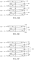
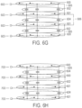
- FIG. 6 is the electrical form for the multi-layer, planar coil stack-ups that are depicted in FIG. 4 .
- FIGS. 6A, 6B, 6C , 6D , and 6I are unterminated and thus do not have direct electrical connections between layers in accordance with embodiments of the invention, while FIGS. 6E, 6F , 6G, 6H , and 6J are terminated and have serial and/or parallel connections between layers, depending on the configuration and, as such, do not fall within the scope of the invention.
Landscapes
- Engineering & Computer Science (AREA)
- Power Engineering (AREA)
- Computer Networks & Wireless Communication (AREA)
- Signal Processing (AREA)
- Coils Or Transformers For Communication (AREA)
- Coils Of Transformers For General Uses (AREA)
- Parts Printed On Printed Circuit Boards (AREA)
- Shielding Devices Or Components To Electric Or Magnetic Fields (AREA)
Description
- The present application claims priority to
U.S. Provisional Patent Application No. 62/512,544, filed May 30, 2017 - This patent application describes a wireless power transfer coil assembly as it pertains to wireless charging through use of magnetic resonant induction. The wireless power transfer coil assembly described herein can be used as part of the sending or as part of the receiving wireless power transfer apparatus.
- Resonant induction wireless charging makes use of an air core transformer consisting of two concentric coils displaced along a common coil axis. Electrical power is sent from the sending apparatus to the receiving apparatus by means of magnetic flux linkage between the two transfer coils. A high frequency alternating current flowing in the primary coil induces an alternating current into the secondary coil.
- As the wireless power transfer operating frequency is significantly higher than line frequency, typically 20 kHz and higher, solid wire has significantly elevated AC losses with respect to direct current due to the skin effect. In order to limit AC resistance, wireless power transfer coil conductors are typically implemented as multiple, independently insulated small diameter conductors connected in parallel, generally gathered together into a rope lay configuration. Wire of this type is referred to as Litz wire. Litz wire has a number of disadvantages in this application. Litz wire has poor utilization of cross-sectional area due to void space between the individual wires and also due to the significant portion of the cross-section occupied by individual wire insulation. The insulation and void space volumes make heat removal from the Litz bundle interior difficult. Finally, Litz wire is costly and assembly operations involving Litz wire especially wire forming and connector attachment are labor intensive.
- A method of designing and constructing resonant induction transfer coils that avoids the disadvantageous use of Litz wire is desired.
-
US 2013/222101 A1 concerns a coil component that includes: an insulating resin layer provided between a first planar spiral conductor formed on a back surface of a first substrate and a second planar spiral conductor formed on a back surface of a second substrate; an upper core covering a third planar spiral conductor formed on a front surface of the first substrate on which the insulating resin layer is formed; and a lower core covering a fourth planar spiral conductor formed on a front surface of the second substrate on which the insulating resin layer is formed. Similarly,EP 3016231 A1 describes a power transmission device having a surface a part of which defines a power transmission plane. The device is suitable for the wireless charging of mobile devices within vehicles. The device includes: a power transmission coil structure including 2N planar coils laminated in a perpendicular direction to the power transmission plane and wirelessly transmitting AC power to a power receiving device via the power transmission plane and being disposed on a side toward the power transmission plane; and a magnetic substance disposed on a side of the power transmission coil opposite from the power transmission plane, wherein the 2N planar coils constitute coil groups including a coil group in which an i'th closest planar coil to the power transmission plane out of the 2N planar coils and the i'th-closest planar coil to the magnetic substance out of the 2N planar coils are connected in series, and the coil groups are connected in parallel to each other.US 2015/077208 A1 describes a parallel-trace spiral coil comprising a plurality of electrically-isolated, parallel connected metal traces with high Q factor for use in bio-medical implants. - The invention is a resonant induction wireless power transfer coil as defined in the appended claims.
- A resonant induction, wireless power transfer coil includes a printed circuit board backed by a layer of flux guiding ferrite magnetic material inside a weatherproof enclosure. Additional components include resonating capacitors, rectifiers and post-rectification ripple filters that are included in the weatherproof enclosure. The multiple, independent individual printed circuit board traces correspond to the multiple independent Litz wire conductors present in conventional transfer coils. Trace width is selected to minimize conductor eddy currents and proximity effects. The overall trace pattern insures current sharing among multiple traces. The resulting planar spiral inductor described herein has low AC resistance and can be easily and inexpensively manufactured as a conventional printed circuit board.
- Sample embodiments include a resonant induction wireless power transfer coil including a 2n-layer coil stack, where n is a positive integer. The 2n-layer coil stack includes a dielectric connected to operate in a differential mode and having a first side and a second side, a first conductor pattern including a first plurality of conductors wound in a spiral on the first side of the dielectric to provide a forward current path conductor, and a second conductor pattern comprising a second plurality of conductors wound in a spiral on the second side of the dielectric to provide a return current path conductor. The second conductor pattern is aligned with the first conductor pattern whereby the second conductor pattern reinforces magnetic flux generated by the first conductor pattern. The first and second conductor patterns are placed relative to one another so as to provide flux transmission in a same direction, and a capacitance between each layer of the coil stack is selected such that the 2n-layer coil stack is self-resonating at a designed self-resonating frequency fr = 1÷(2π√(LC)) that is being used for wireless power transfer with another wireless power coil of a wireless power transfer apparatus, where L= equivalent coil inductance of the 2n-layer coil stack and C = equivalent capacitance of the 2n-layer coil stack. The 2n-layer coil stack is characterised in that the first and second conductor patterns are not directly electrically connected.
- The dielectric may comprise a printed circuit board having a first side and a second side, the first conductor pattern comprising a first plurality of conductors wound in a spiral on the first side of the printed circuit board, and the second conductor pattern comprising a second plurality of conductors wound in a spiral on the second side of the printed circuit board. At least one electrical connection may be provided to electrically connect respective conductors of the first and second conductor patterns. The electrical connections may comprise at least one throughhole through the printed circuit board or at least one or more of a clamp, a lug, and a terminal. The throughholes may also be plated offset throughholes.
- The first and second conductor patterns may comprise at least 2 turns of conductor configured as a square, flat planar spiral and the first and second plurality of conductors may each comprise at least two independent conductors.
- The trace thickness is limited by the skin depth at the operating frequency as it contributes to AC resistance. Skin depth δ at a resonant induction wireless power operating frequency is given by

- The trace width is limited by the allowable conductor eddy currents. Eddy current losses for a conductive element in a uniform magnetic field are

- The wireless power transfer coil may further include coil terminals and associated throughholes in the center of the first and second conductor patterns or at an outer edge of the first and second conductor patterns and an outer edge of the printed circuit board.
- The wireless power transfer coil also may comprise a multi-layer coil stack comprising 2n layers having the first and second conductor patterns, where n is a positive integer. In a first configuration, where n=1, the multi-layer coil stack comprises a first conductor pattern providing a forward current path conductor, a second conductor pattern providing a return current path conductor, and a dielectric connected to operate in a differential mode that is provided between the first conductor pattern and the second conductor pattern.
- In an embodiment, where n=2, the multi-layer coil stack respectively comprises a first conductor pattern providing a forward current path conductor, a second conductor pattern providing a return current path conductor, a third conductor pattern providing a forward current path conductor, a fourth conductor pattern providing a return current path conductor, a first dielectric provided between the first conductor pattern and the second conductor pattern connected to operate in a differential mode, a second differential mode dielectric provided between the third conductor pattern and the fourth conductor pattern connected to operate in a differential mode, and a third differential mode dielectric provided between the second conductor pattern and the third conductor pattern connected to operate in a differential mode.
- In an alternate embodiment, where n=2, the multi-layer coil stack respectively comprises a first conductor pattern providing a forward current path conductor, a second conductor pattern providing a return current path conductor, a third conductor pattern providing a return current path conductor, a fourth conductor pattern providing a forward current path conductor, a first dielectric provided between the first conductor pattern and the second conductor pattern connected to operate in a differential mode, a second dielectric provided between the third conductor pattern and the fourth conductor pattern connected to operate in a differential mode, and a third dielectric provided between the second conductor pattern and the third conductor pattern connected to operate in a common mode.
- In still another embodiment, where n=2, the multi-layer coil stack respectively comprises a first conductor pattern providing a first forward current path conductor, a second conductor pattern providing a second forward current path conductor, a third conductor pattern providing a first return current path conductor, a fourth conductor pattern providing a second return current path conductor, a first dielectric provided between the first conductor pattern and the second conductor pattern connected to operate in a common mode, a second dielectric provided between the third conductor pattern and the fourth conductor pattern connected to operate in a common mode, and a third dielectric provided between the second conductor pattern and the third conductor pattern connected to operate in a differential mode.
- The multi-layer coil stack may further include terminals implemented as independent tabs offset along an edge of each printed circuit board to facilitate connection to independent terminal pairs of respective conductor patterns of each printed circuit board. Vias or terminals may also be provided to connect respective conductor patterns through a middle of the respective boards. Second terminals may also be implemented as independent tabs offset along a center of each printed circuit board to facilitate connection to independent terminal pairs of respective conductor patterns of each printed circuit board.
- The terminals may be implemented as independent tabs offset along a center of each printed circuit board to facilitate connection to independent terminal pairs of respective conductor patterns of each printed circuit board. The vias or terminals may connect respective conductor patterns through an outer edge of the respective circuit boards.
- The dielectrics connected to operate in a differential mode should be able to withstand the maximum voltage difference between conductors. In sample embodiments, the dielectrics connected to operate in a common mode may be minimized to manufacturing tolerances because voltages across the dielectrics connected to operate in a common mode are close to zero.
- The wireless power transfer coil may be incorporated into a wireless power transfer coil assembly further including an enclosure, a ferrite layer, and an eddy current shield. The wireless power transfer coil, ferrite layer, and eddy current shield may be disposed in parallel within the enclosure.
- The ferrite layer may comprise a ferrite backing layer bonded to ferrite bars, tiles, or plates of constant thickness so as to hold the ferrite bars together as a single assembly wherein a tiling density of the ferrite is continuous or near continuous near a center of the wireless power transfer coil and the tiling density is reduced progressively as a perimeter of the wireless power transfer coil is approached. Alternatively, the ferrite layer may comprise a composite magnetic structure including ferrite powder combined with a binding material and injection molded to form a composite ferrite layer that is thicker at a center thereof and thinner at a perimeter thereof. On the other hand, the eddy current shield may comprise an electrically conductive sheet or a conductive film deposited on a dielectric substrate that is adapted to intercept and dissipate residual magnetic flux not diverted by the ferrite layer. The assembly may also include mechanically conformal, electrically non-conductive layers disposed between the enclosure and the wireless power transfer coil, between the wireless power transfer coil and the ferrite layer, and between the ferrite layer and the eddy current shield. These electrically non-conductive layers are adapted to provide mechanical support, heat removal, and physical spacing for the wireless power transfer coil and the ferrite layer.
- The enclosure may further include an enclosed volume containing power control, communication, and/or sensor electronics. The circuitry may include resonating capacitors, power control circuitry, communications circuitry, and circuitry adapted to provide object detection functions. The resonating capacitors may be in the form of a thin, multi-layer, metalized dielectric sheet implemented as an additional layer located between the ferrite layer and the enclosure. Alternatively, the resonating capacitors may be in the form of thin, large area metalized dielectric films located on a low field intensity side of the ferrite layer.
- At least two of the wireless power transfer coils may be stacked and connected in parallel to increase winding ampacity or stacked and connected in series to increase winding inductance.
- A sensor aperture may be located at a center of the wireless power transfer coil and includes sensor electronics while allowing for bi-directional passage of sensor or communications signals to/from respective sides of the wireless power transfer coil assembly. The sensor electronics may include a light pipe, acoustic waveguide, electromagnetic waveguide, or dielectric waveguide for sensing and communications. Also, the electromagnetic waveguide may have high-pass or bandpass frequency selective surfaces adapted to avoid the generation of eddy currents. In addition, the dielectric waveguide may be implemented as a single wire Goubau transmission line that is adapted to avoid eddy current generation.
- In certain embodiments, the first conductor pattern may be a flat spiral of conductive tape having a thickness that is no thicker than four times a skin depth of the first conductor pattern at an operating frequency, where skin depth δ at a resonant induction wireless power operating frequency is given by

-
-
FIG. 1A shows the top side trace pattern of the resonant induction wireless power transfer coil implemented as a center-fed double sided printed circuit board. -
FIG. 1B shows the bottom side pattern of the resonant induction wireless power transfer coil ofFIG. 1A as viewed through the top side. -
FIG. 1C shows the superimposed top side and bottom side patterns ofFIGS. 1A and 1B . -
FIG. 2A shows the top side trace pattern of the resonant induction wireless power transfer coil implemented as an outer-edge fed double sided printed circuit board. -
FIG. 2B shows the bottom side pattern of the resonant induction wireless power transfer coil ofFIG. 2A as viewed through the top side. -
FIG. 2C shows the superimposed top side and bottom side patterns ofFIGS. 2A and 2B . -
FIGS. 3A-3H show individual conductor patterns of respective layers of the resonant induction wireless power transfer coil implemented as an outer-edge terminated multi-layer, multi-conductor coil implemented as an eight-layer printed circuit board as viewed through the top side. -
FIG. 3I shows the composite eight-layer stack of rectangular planar coils ofFIGS. 3A-3H looking through the superimposed layers from the top side. -
FIG. 3J shows a sample arrangement of the composite eight-layer stack of rectangular planar coils ofFIGS. 3A-3H having offset plated through holes. -
FIG. 4A shows a cross-sectional view of a sample multi-layer coil stack comprising 2n layers, where n=1. -
FIG. 4B shows a basic four-layer coil (n=2) having alternative forward and return current path conductors. -
FIG. 4C shows a basic four-layer coil (n=2) having differential mode dielectrics and forward current paths on outer layers and return current paths on inner layers. -
FIG. 4D shows a basic four-layer coil (n=2) having non-interleaved conductors with common mode dielectrics. -
FIG. 5A shows a perspective view of a coil stack constructed of multiple, independent multi-tabbed multi-layer planar coils of the type illustrated inFIGS. 1-4 and having an outside edge termination. -
FIG. 5B shows a perspective view of a coil stack constructed of multiple, independent multi-tabbed multi-layer planar coils of the type illustrated inFIGS. 1-4 and having a center-fed termination. -
FIG. 5C shows a perspective view of a coil stack constructed of multiple, independent multi-tabbed multi-layer planar coils of the type illustrated inFIGS. 1-4 and having both outside edge and center-fed terminations. -
FIG. 6A shows unterminated two-layer parallel coils of a distributed lumped-element electrical representation of planar coils in accordance with an embodiment of the invention. -
FIG. 6B shows unterminated four-layer interleaved parallel coils of a distributed lumped-element electrical representation of planar coils in accordance with another embodiment of the invention. -
FIG. 6C shows an alternate arrangement of unterminated four-layer interleaved parallel coils of a distributed lumped-element electrical representation of planar coils in accordance with another embodiment of the invention. -
FIG. 6D shows unterminated four-layer non-interleaved parallel coils of a distributed lumped-element electrical representation of planar coils in accordance with another embodiment of the invention. -
FIG. 6E shows terminated two-layer parallel coils of a distributed lumped-element electrical representation of planar coils, which is not an embodiment of the invention. -
FIG. 6F shows terminated four-layer interleaved parallel coils of a distributed lumped-element electrical representation of planar coils, which is not an embodiment of the invention. -
FIG. 6G shows an alternate arrangement of terminated four-layer interleaved parallel coils of a distributed lumped-element electrical representation of planar coils, which is not an embodiment of the invention. -
FIG. 6H shows terminated four-layer non-interleaved parallel coils of a distributed lumped-element electrical representation of planar coils, which is not an embodiment of the invention. -
FIG. 6I shows unterminated four-layer interleaved series coils of a distributed lumped-element electrical representation of planar coils in accordance with another embodiment of the invention. -
FIG. 6J shows terminated four-layer interleaved series coils of a distributed lumped-element electrical representation of planar coils, which is not an embodiment of the invention. -
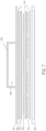
FIG. 7 shows a cross-sectional view of a vehicle side transfer coil assembly. -
FIG. 8 shows a cross-sectional view of a vehicle side transfer coil assembly. -
FIG. 9 shows a cross-sectional view of a vehicle side transfer coil assembly with a sensor aperture. -
FIG. 10 shows a cross-sectional view of a vehicle side transfer coil assembly with a sensor aperture. - The wireless power transfer coil assembly and associated method described herein may be understood more readily by reference to the following detailed description taken in connection with the accompanying figures and examples, which form a part of this disclosure. It is to be understood that this description is not limited to the specific products, methods, conditions or parameters described and/or shown herein, and that the terminology used herein is for the purpose of describing particular embodiments by way of example only and is not intended to be limiting of any claimed subject matter. Similarly, any description as to a possible mechanism or mode of action or reason for improvement is meant to be illustrative only, and the subject matter described herein is not to be constrained by the correctness or incorrectness of any such suggested mechanism or mode of action or reason for improvement. Throughout this text, it is recognized that the descriptions refer both to methods and systems/software for implementing such methods.
- A detailed description of embodiments of the invention, and arrangements that are not embodiments, will now be described with reference to
FIGS. 1-10 . Although this description provides a detailed example of possible implementations, it should be noted that these details are intended to be exemplary and in no way delimit the scope of the inventive subject matter. -
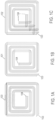
FIG. 1 is a representation of a non-self-resonating coil structure including a center-fed double sided, printed circuit board resonant induction wireless power transfer coil having 3 ¼ turns configured as a square, flat, planar spiral. The wireless power transfer coil may have at least 2 turns.FIG. 1A shows the topside conductor pattern 100 comprised of four independent conductors, although two or more independent conductors may be used.FIG. 1B shows the bottomside conductor pattern 101 as seen looking through the printed circuit board. The bottomside conductor pattern 101 is the same as the top side conductor pattern flipped left to right along the vertical centerline and rotated 90 degrees clockwise. It will be appreciated that theconductor patterns side conductor pattern 100 and bottomside conductor pattern 101 should sufficiently align to maximize magnetic flux generation by reinforcing the flux generated by each pattern by the other.FIG. 1C shows the superimposed top side andbottom side patterns 102. Plated through holes 103 (also commonly known as vias) may electrically connect the top 100 and bottom 101 trace patterns. Coil terminals and associated plated throughholes 104 are shown at the center of thecoil 102. Connection to off board components such as coil resonating capacitors may be accomplished by means of multiple, parallel but independent conductors thereby extending the advantageous planar multiple independent conductor structure. For a self-resonating coil,terminals 104 are connected directly to power, where in the non-self-resonating coil, the terminals connect to the resonating capacitors. Also, in alternate arrangements, connection between the top andbottom layers holes 103. - As shown in
FIG. 1C , top side conductors are placed directly over the corresponding bottom side conductors where possible as such placement allows uniform flux transmission and the top and bottom windings intercept the same flux distribution. The result is a symmetrical flatspiral inductor 102 having two layers and a total of 6 ½ turns. Because current flows in the same direction in the top 100 and the bottom 101 sections, magnetic flux generated by the top and bottom layers is reinforced. In this example, if current is fed into the topconductor layer terminals 104, the current flow is in the clockwise direction when looking through the board from the top. Current fed into the bottomconductor layer terminals 104 results in a counter-clockwise current flow. Connecting the top and bottom spirals doubles the number of turns and increases the total inductance by a factor of four. -
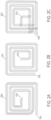
FIG. 2 is an example of a non-self-resonating coil structure including an outer-edge fed, double-sided, printed circuit board, resonant induction wireless power transfer coil having 3 ¼ turns configured as a square, flat, planar spiral. the wireless power transfer coil may have at least 2 turns.FIG. 2A shows the topside conductor pattern 200 comprised of four independent conductors, although two or more independent conductors may be used.FIG. 2B shows the bottomside conductor pattern 201 as seen looking through the printed circuit board. The bottomside conductor pattern 201 is the same as the top side conductor pattern flipped left to right along the vertical centerline and rotated 90 degrees clockwise. It will be appreciated that theconductor patterns FIG. 2C shows the superimposed top side andbottom side patterns 202. Plated through holes 103 (also commonly known as vias) may electrically connect the top 200 and bottom 201 trace patterns. Coil terminals and associated plated throughholes 103 are shown at the outer corner of thecoil 202. Connection to off board components such as coil resonating capacitors may be accomplished by means of multiple, parallel butindependent conductors 104 thereby extending the advantageous planar multiple independent conductor structure. For a self-resonating coil,terminals 104 are connected directly to power, where in the non-self-resonating coil, the terminals connect to the resonating capacitors. Also, the connection between the top and bottom layers may be implemented as an electrical structure such as a clamp, lug, or terminal instead of the plated throughholes 103. - As shown in
FIG. 2C ,top side conductors 200 are placed directly over the correspondingbottom side conductors 201 where possible as such placement allows uniform flux transmission and the top and bottom windings intercept the same flux distribution. The result is a symmetrical flatspiral inductor 202 having two layers and a total of 6 ½ turns. Because current flows in the same direction in the top 200 and the bottom 201 sections, magnetic flux generated by the top and bottom layers is reinforced. In this example, if current is fed into the topconductor layer terminals 104, the current flow is in the counter-clockwise direction when looking through the board from the top. Current fed into the bottomconductor layer terminals 104 results in a clockwise current flow. Connecting the top and bottom spirals doubles the number of turns and increases the total inductance by a factor of four. - In the arrangements of
FIGS. 1 and2 , the number of traces operated in parallel to constitute a single winding conductor is determined by the operating frequency, the trace material conductivity, and the operating current. Narrow trace widths limit conductor eddy currents in the trace width dimensions and also maintain uniform current density across the individual trace cross-sections. Eddy current losses for a conductive element in a uniform magnetic field are
- Trace thickness is limited by the skin depth at the operating frequency as it contributes to AC resistance. Skin depth δ at typical resonant induction wireless power frequencies is given by δ= √(2σ/ωµ) where σ is the conductor resistivity in Ohm-Meters, ω is the operating frequency in radians per second and µ is the magnetic permeability of the trace material.
- The number of parallel traces is determined by the operating current and the ampacity of the trace for the specified trace cross-sectional area and environmental conditions.
FIGS. 1 and2 show arrangements using 4 parallel conductors but any number may be used. Adjacent trace-to-trace separation distance within a turn ensemble can be small, limited only by printed circuit board manufacturing design rules as trace-to-adjacent-trace voltages within the same ensemble are near zero. Turn-to-turn spacing between conductor ensembles must be sufficient to provide adequate voltage isolation between adjacent turns. Turn-to-turn voltage is proportional to the ratio of the turn diameters. The printed circuit board dielectric layer thickness should be sufficient to prohibit dielectric breakdown. - The longer outer conductors of the top
side conductor pattern 200 are connected to the shorter inside conductors of the bottomside conductor pattern 201. Swapping conductors from inside to outside in this fashion equalizes conductor length and inductance. Equalized length and inductance equalizes resistance and reactance, which equalizes current distribution between conductors. Top side and bottom side conductors are superimposed. Magnetic flux flows through the inter-conductor gaps. In certain arrangements, all conductor traces are of equal length. - As will be discussed below, the two-layer structure depicted in
FIGS. 1 and2 can be extended to 2n-layers, where n is any positive integer value. The 2n-layer coil structure can be made to be self-resonating by designing the capacitance between coil layers, such that self-resonating frequency,
holes 104 are connected directly to power. -
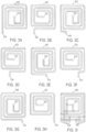
FIG. 3 is a representation of a multi-layer, multi-conductor pair, edge terminated coil.FIG. 3 depicts an eight-layer stack up of individual coils that are roughly 3 ¼ to 3 ½ turns each.Conductor pattern 300 is the top layer (layer 1), 301 islayer 2, 302 islayer 3, 303 islayer 4, 304 islayer 5, 305 islayer 6, 306 islayer 7, and 307 is the bottom layer (layer 8). Conductor pairs 300 and 301, 302 and 303, 304 and 305, 306 and 307 follow the same criteria as depicted inFIG. 2 .Coil terminals 104 ofFIGS. 3A, 3C, 3E, and 3G receive input signals andcoil terminals 104 ofFIGS. 3B, 3D, 3F, and 3H provide output signals for a clockwise current configuration. Plated throughholes 103 may comprise blind and/or buried vias that connect certain layers while isolating other layers, depending on coil configuration. It will be appreciated that the plated throughholes 103 need not all fall directly on top of one another. Individual paired connections may be offset with independent plated throughhole 103 patterns. An arrangement showing offset plated throughholes 103 is depicted inFIG. 3J . -
FIG. 3I is the composite eight-layer stack up looking through the printed circuit board or laminate assembly from the top side.Conductor pattern 308 is the superposition of patterns 300-307. In this arrangement, plated throughholes 103 pass current between layers.Coil terminals 104 all lie on the outer edge of the coil assembly. In an alternative arrangement, an opening in the center of the coil structure may be provided that would allow current to be passed between layer pairs by means of an electrically conductive clamping mechanism. - It will be appreciated by those skilled in the art that the coil stack of
FIG. 3 may be provided within a multi-laminated assembly that could be implemented as a printed circuit board (PCB). -
FIG. 4 shows a cross-sectional view of four sample multi-layer coil stacks comprising 2n layers, where "n" can be any positive integer. The conductor patterns depicted inFIGS. 1 ,2 and3 can apply to the cross-sections depicted inFIG. 4 . -
FIG. 4A shows a basic two-layer case (n=1), where 400 is the forward current path conductor, 401 is the return current path conductor, and 402 is the differential mode dielectric. -
FIG. 4B shows the basic four-layer case (n=2), where again 400 is the forward current path conductor, 401 is the return current path conductor, and 402 is the differential mode dielectric. The arrangement ofFIG. 4B is essentially a stack-up of two, two-layer panels depicted inFIG. 4A with an additional differentialmode dielectric layer 402 in between. This implementation includes alternating forward and return current path conductors. To extendFIG. 4B to six layers or more (n=3+), thepattern 404 which includes adifferential mode dielectric 402, forwardcurrent path conductor 400, adifferential mode dielectric 402, and returncurrent path conductor 401 is repeated. -
FIG. 4C shows a basic four-layer case (n=2), where again 400 is the forward current path conductor, 401 is the return current path conductor, 402 is the differential mode dielectric, and 403 is a common mode dielectric layer. This configuration is similar toFIG. 4B except that the bottom two layers are inverted, such that the forward currents travel on the top andbottom layers 400 and the return currents travel on theinner layers 401. This results in acommon mode dielectric 403 since the returncurrent path conductors 401 are electrically in parallel with one another. To extendFIG. 4C to six-layers or more (n=3+), thepattern 405 which includes acommon mode dielectric 403, either a forwardcurrent path conductor 400 for n=odd or a reversecurrent path conductor 401 for n=even, adifferential mode dielectric 402, and either a reversecurrent path conductor 401 for n=odd or a forwardcurrent path conductor 400 for n=even is repeated. -
FIG. 4D shows the basic four-layer case (n=2), where again 400 is the forward current path conductor, 401 is the return current path conductor, 402 is the differential mode dielectric, and 403 is a common mode dielectric layer. This configuration is similar toFIG. 4A , except that the top and bottom layers each have an additional layer added in parallel for carrying the forward and reverse currents. This results incommon mode dielectrics 403 between the top twoconductors 400 and bottom twoconductors 401 and onedifferential mode dielectric 402 in the center of the four-layer stack-up. To extendFIG. 4D to six-layers or more (n=3+), thepattern 406 on the top side, which includes acommon mode dielectric 403, and a forwardcurrent path conductor 400 is repeated. Also, thepattern 407 on the bottom side, which includes acommon mode dielectric 403, and a reversecurrent path conductor 401, is repeated. - It will be appreciated that the coil configurations of
FIGS. 4A through 4D may be used in the creation of other arrangements of more coil layers. For example, six differential pairs of coil assemblies may be implemented as multiple instances and combinations of 4-layer stack-ups as depicted inFIGS. 4B, 4C, and 4D to provide a 24-layer coil design. -
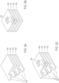
FIG. 5 depicts perspective views for coil stacks that may be constructed of multiple, independent, multi-layer coil implementations as shown inFIGS. 1-4 . -
FIG. 5A is a physical representation of an edge-terminated coil stack that may be constructed of multiple, independent, multi-layer coil implementations as depicted inFIGS. 1-4 . In the edge-terminated coil stack ofFIG. 5A , four independent planar coils are provided that implement the conductor patterns ofFIG. 3 .Item 500 is a planar coil that includes n layers ofconductor patterns Item 501 is a planar coil that includes n layers ofconductor patterns Item 502 is a planar coil that includes n layers ofconductor patterns Item 503 is a planar coil that includes n layers ofconductor patterns Coil terminals 504 may be implemented as independent "tabs" of planar coils 500-503 that are offset along the edge to facilitate connection to independent terminal pairs as illustrated. The signals may pass between layers using vias or terminals connecting the boards through the middle as in the arrangements illustrated inFIGS. 1-4 . In the edge-terminated coil stack ofFIG. 5A , an edge pattern, spiraling from the edge inward, is provided and the boards pass signals through vias or terminals (not shown) connecting through the middle of the respective boards. -
FIG. 5B is a physical representation of a center-fed coil stack that may be constructed of multiple, independent, multi-layer coil implementations as depicted inFIGS. 1-4 . In the center-fed coil stack ofFIG. 5B , four independent planar coils are provided that implement the conductor patterns ofFIG. 3 .Item 500 is a planar coil that includes n layers ofconductor patterns Item 501 is a planar coil that includes n layers ofconductor patterns Item 502 is a planar coil that includes n layers ofconductor patterns Item 503 is a planar coil that includes n layers ofconductor patterns Coil terminals 504 may be implemented as independent "tabs" of planar coils 500-503 that are offset along the center core to facilitate connection to independent terminal pairs as illustrated. The signals may pass between layers using vias or terminals connecting the boards through the middle as in the arrangements illustrated inFIGS. 1-4 . In the center-fed coil stack ofFIG. 5B , a center-fed pattern, spiraling from the center outward, is provided and the boards pass signals through vias or terminals (not shown) connecting through an outer corner of the respective boards. -
FIG. 5C is a physical representation of a coil stack that has both edge-terminations and center-terminations. Each coil stack may be constructed of multiple, independent, multi-layer coil implementations as depicted inFIGS. 1-4 . In the coil stack ofFIG. 5C , are four independent planar coils are provided that implement the conductor patterns ofFIG. 3 .Item 500 is a planar coil that includes n layers ofconductor patterns Item 501 is a planar coil that includes n layers ofconductor patterns Item 502 is a planar coil that includes n layers ofconductor patterns Item 503 is a planar coil that includes n layers ofconductor patterns Coil terminals 504 may be implemented as independent "tabs" of planar coils 500-503 that are offset along the edge and along the center core to facilitate connection to independent terminal pairs as illustrated. The signals may pass between layers using vias or terminals connecting the boards through the middle as in the arrangements illustrated inFIGS. 1-4 . In the coil stack ofFIG. 5C , having both edge terminals and center terminals, the coil stack can be configured to be either an edge-fed or center-fed coil stack. - Utilizing multiple, independent, multi-layer coil stacks as illustrated in
FIG. 5 may provide cost benefits in manufacturing where the total number of coil conductor layers is large. Rather than producing one printed circuit board of 16 to 24 layers, for example, four to six 4-layer coil stacks may be integrated into one assembly. Additional arrangements could include "m" coil stacks, wherein "m" is any positive integer greater than one (e.g., two coil stacks with two tabs or ten coil stacks with ten tabs). -
FIG. 6 is the electrical form for the multi-layer, planar coil stack-ups that are depicted inFIG. 4 .FIGS. 6A, 6B, 6C ,6D , and6I are unterminated and thus do not have direct electrical connections between layers in accordance with embodiments of the invention, whileFIGS. 6E, 6F ,6G, 6H , and6J are terminated and have serial and/or parallel connections between layers, depending on the configuration and, as such, do not fall within the scope of the invention. -
FIG. 6A is the distributed element representation of a two-layer coil with a cross-section that is depicted inFIG. 4A . The forward current pathinductive elements 600 and return current pathinductive elements 601 correspond to the forwardcurrent path conductor 400 and returnpath conductor 401, respectively. The differential mode dielectriccapacitive elements 602 correlate with thedifferential mode dielectric 402. The coil electrical terminals are noted as 603. -
FIG. 6B is the distributed element representation of a four-layer coil scenario with a cross-section that is depicted inFIG. 4B . The forward current pathinductive elements 600, return current pathinductive elements 601, and differential mode dielectriccapacitive elements 602 correlate with 400, 401 and 402, respectively. The coil electrical terminals are noted as 603. -
FIG. 6C is the distributed element representation of a four-layer coil scenario with a cross-section that is depicted inFIG. 4C . The forward current pathinductive elements 600, return current pathinductive elements 601, and differential mode dielectriccapacitive elements 602 correlate with 400, 401 and 402, respectively. The coil electrical terminals are noted as 603. This configuration is similar toFIG. 6B , except that the bottom two layers are inverted, such that the forward currents travel on the top andbottom layers 600 and the return currents travel on theinner layers 601. This results in the common mode dielectriccapacitive elements 604 that correlate with thecommon mode dielectric 403. -
FIG. 6D is the distributed element representation of a four-layer coil scenario with a cross-section that is depicted inFIG. 4D . This configuration is similar toFIG. 6A , except that the top and bottom layers each have an additional layer added in parallel for carrying the forward and reverse currents. The forward current pathinductive elements 600, return current pathinductive elements 601, and differential mode dielectriccapacitive elements 602 correlate with 400, 401 and 402, respectively. The coil electrical terminals are noted as 603. The common mode dielectric capacitive elements are noted as 604. -
FIGS. 6E, 6F ,6G, and 6H are identical toFIGS. 6A, 6B, 6C , and6D , respectively, with the exception that the planar coil layers are connected to one another with a series connection of forward current path and return current pathinductive elements 605, and as such do not fall within the scope of the invention. Optionally, the middle two layers inFIGS. 6F and6G may be connected as shown by theconnector 606 in dashed line. Electrically,connections 606 are not required, but they may provide benefit in manufacturing. -
FIG. 6I is a distributed element representation of a four-layer interleaved coil structure that is fully series resonant and only has two terminals. This embodiment of the invention does not require plated through holes between planar coil layers as the inductive and capacitive elements create a series LC resonance. -
FIG. 6J is a distributed element representation of a four-layer interleaved coil structure that is fully parallel resonant and only has two terminals. This arrangement does incorporate plated through holes that serially connect the inductive elements fromlayer 1 to layer 2 to layer 3 and then to layer 4 and as such does not fall within the scope of the invention. This structure results in a parallel resonance from the series inductive elements and the parallel capacitance between coil windings. -
FIG. 7 is a cross-sectional representation of a vehicle sidetransfer coil assembly 700. Thetransfer coil assembly 700 is contained within an environmentally sealed enclosure including thecoil assembly cover 701 and thecoil assembly enclosure 702. The printed circuit board containing the coil conductors ofFIGS. 1A-1C is indicated by 703. Directly abovecoil conductors 703 is theferrite backing layer 704, a non-conductive adhesive sheet, tape, film or cloth bonded to the ferrite which holds the ferrite bars or tiles together as a single assembly. Flux density is strongest at the center of the coil assembly. Ferrite layer spatial density as well as ferrite thickness must be adequate to avoid saturation. Because flux intensity decreases towards the coil perimeter, ferrite layer spatial density and/or thickness can be thinned while still avoiding saturation. Ferrite layer thinning is desirable as a means of reducing transfer coil weight and cost. Theferrite layer 705 is implemented as an array of ferrite bars or plates having constant thickness. The array tiling is continuous or near continuous at the center of the coil. Tiling density is reduced progressively as the perimeter is approached. The ferrite layer tiling has gaps as required to allow protrusion of the coil terminal conductors and other protrusions or penetrations as required. - The
ferrite bar tiling 705 andferrite backing layer 704 are replaced with a single composite magnetic structure including ferrite powder combined with a binding material such as a thermoplastic or resin and possibly additional substances such as thermally conductive, electrically insulating powder to improve thermal conductivity, injection molded or otherwise shaped to final or near final form. Magnetic flux is most intense in the center of thetransfer coil 703 diminishing towards the perimeter. This means thecomposite ferrite layer 705 can be thicker at the center where the flux is the most intense to avoid ferrite material saturation and thinner at the perimeter to reduce weight and material cost. Material composition can vary spatially to tailor thermal and magnetic properties as a function of location. Passages for cooling fluid can be included where and as required. - An
eddy current shield 706 is implemented as an electrically conductive sheet or layer that intercepts and dissipates the residual magnetic flux not diverted by theferrite layer 705. Eddycurrent shield 706 can be a metallic plate providing structural strength to thetransfer coil assembly 700. Non-ferrous metals with relative permeability near one are preferred in this use on order to avoid disturbance of the flux steering action of theferrite layer 705. Alternatively, theeddy current shield 706 can be a conductive film deposited on a dielectric substrate. Theeddy current shield 706 can also be integrated into the coil assembly enclosure by attaching theeddy current shield 706 to the inside surface of theenclosure 702 or by making the enclosure from aluminum. -
Layers 707 are mechanically conformal, electrically non-conductive layers providing mechanical support, heat removal by means of thermal conductivity and physical spacing for the conductor printedcircuit board 703 and the ferriteflux steering layer 705. The ferriteflux steering layer 705 should not be in contact or in near contact of the conductor printedcircuit board 703 or theeddy current shield 706 in order to avoid excessive proximity effect resistive losses in the former and excessive eddy current losses in the latter. The spacing layers 707 can be made of conventional elastomeric compression pads used as gap fillers between heat generating circuitry and heat removal surfaces. Alternatively, spacing layers 707 can be implemented as open cell foam material infused with a heat conductive liquid such as mineral oil. Improved cooling fluid flow is obtained by placing holes or slots as needed in the spacing layers 707. On the conductor printedcircuit board 703, slots are placed between conductor traces or between turns to preserve conductor continuity. Thecoil assembly enclosure 701 also may include a separateenclosed volume 708 containing other system components such as resonating capacitors, rectifiers, post-rectification ripple filter components, control, communications, foreign object and living object detection circuity, and interface electronics. - In
FIG. 7 , the printedcircuit board 703 is double-sided with conductive traces on the top and bottom sides but having no inter-layers. Multiple printed circuit boards or a multi-layer printed circuit board can be used with the turns connected in parallel to increase ampacity or in series to increase inductance. -
FIG. 8 is a cross-sectional representation of a vehicle sidetransfer coil assembly 800. Additional printed circuit boards or layers can be included as needed to implement transfer coil alignment, near field communications, foreign object/living object detection, or E-field faraday shielding functions. The resonating capacitor can be implemented as a printed circuit board containing an array of surface mount capacitors, the multiple capacitors allowing increased capacitance, and voltage rating. Alternatively, the resonating capacitors can be physically realized as a thin, multi-layer, metalized dielectric sheet implemented as an additional layer located between theferrite layer 705 and thecoil assembly enclosure 702. InFIG. 8 , anobject detection PCB 809,ferrite isolation layer 810, andcommunication PCB 811 are shown between the conductor printedcircuit board 703 and thecoil assembly cover 702. Thecoil assembly enclosure 702 may include a separateenclosed volume 708 containing other system components such as resonating capacitors, rectifiers, post-rectification ripple filter components, control, communications, foreign object and living object detection circuity, and interface electronics. The resonating capacitors may be realized as thin, large area metalized dielectric films located in thetransfer coil assembly 800 on the low field intensity side of theferrite layer 705. - In an alternative embodiment, a flat spiral of conductive tape or strip replaces the printed
circuit board 703. The tape or strip is placed with the width dimension parallel to the incident magnetic flux in order to minimize eddy currents across the face of the conductor. In order to minimize eddy currents in the thickness dimension, the thickness of the conductive tape or strip is limited to be no thicker than four times the skin depth in the trace conductor at the operating frequency. Non-conductive spacers maintain separation between adjacent spiral turns. The conductive tape or strip conductors are otherwise uninsulated in order to not hinder heat removal. Increased tape or strip width increases conductor ampacity. Tape or strip spirals can be stacked vertically for printed circuit conductors to increase ampacity when wired in parallel, or to increase inductance when wired in series. - Those skilled in the art will appreciate that the ground side transfer coil layers can be identical to the vehicle side coil to improve manufacturing efficiencies.
FIG. 9 is a sample arrangement of a vehicle transfer coil assembly with asensor aperture 900 added.Sensor electronics 901 look intoaperture conduit 902, which terminates withsensor conduit endcap 903. - Commercial resonant induction wireless power equipment typically requires ancillary systems to meet current and expected regulatory requirements. These ancillary systems include coil alignment error detection, communications, foreign object detection, and living object detection all of which are best located at the geometry center of the transfer coil active face. However, the center of the active face has high magnetic flux amplitude prohibiting placement of wiring and electronic circuity at that location.
-
FIG. 9 shows thetransfer coil assembly 700 previously shown inFIG. 7 with a centrally locatedsensor aperture 900. Thisaperture 900 running through the thickness dimension of the transfer coil assembly allows the bi-directional passage of sensor or communications signals from the high magnetic flux intensity front face of the transfer coil assembly through to the low magnetic flux intensity region inside theenclosure volume 708. Thesensor electronics 901 inside theenclosure volume 708 can be optical, optical image, optical video, ultrasonic, as well as microwave, millimeter wave or terahertz wave electromagnetic energy. Components designated as 902 and 903 are the aperture conduit and aperture endcap, respectively. Implantation of the aperture conduit and endcap depends upon the sensor modality. For optical sensors and communications, the conduit can be a non-conductive empty tube, a transparent light pipe, or a spatially coherent or non-coherent fiber optics bundle. Theendcap 903 provides an environmental seal with thetransfer coil cover 702 but can also include an optical lens such as a wide angle or fisheye lens. Theconduit 902 can include optical components such as lens as well. Non-electrically conductive materials are preferred to avoid eddy current generation. For ultrasonic sensor or communications modality, the sensor conduit is an acoustic waveguide. Theendcap 903 provides an environmental seal as before and can include an acoustic lens or diffuser. - For electromagnetic sensor modality, the sensor conductor is an electromagnetic waveguide or transmission line structure. Conventional metallic waveguide or transmission line structures such as stripline transmission line are not suitable due to eddy current generation in the intense magnetic field. Such structures can be made suitable by substituting high-pass or bandpass frequency selective surfaces for the continuous metallic surfaces present in conventional waveguide or transmission line structures. Alternatively, the conduit transmission line can be implemented as a Goubau single wire transmission line with the launcher located on the low magnetic intensity side of the ferrite layer, or with the launcher constructed from frequency selective instead of continuous metallic surfaces. In a sample arrangement, the electromagnetic waveguide is implemented as a conventional dielectric waveguide including a high dielectric constant core surrounded by a low dielectric constant medium. The
endcap 903 provides an environmental seal that can include a dielectric or artificial dielectric lens. Through use of a flexible printed circuit board for the windinglayer 703 and small ferrite tile size or the use of a flexible or non-planarcomposite ferrite layer 705 the transfer coil assembly can be made conformal to a non-planar surface such as a cylinder for ease of mechanical fit, for reduced aerodynamic or hydrodynamic drag or for placement on a vehicle or object having cylindrical or other non-planar form such as underwater autonomous vehicles, artillery shells or similar obj ects. -
FIG. 10 is a cross-sectional representation of a vehicle sidetransfer coil assembly 800 with a sensor aperture added in accordance with an alternative arrangement. As in the arrangement ofFIG. 8 , additional printed circuit boards or layers can be included as needed to implement transfer coil alignment, near-field communications, foreign object/living object detection, or E-field faraday shielding functions. InFIG. 10 , as in the arrangement ofFIG. 8 , anobject detection PCB 809,ferrite isolation layer 810, andcommunication PCB 811 are provided between the conductor printedcircuit board 703 and thecoil assembly cover 702. - While various implementations have been described above, it should be understood that they have been presented by way of example only, and not limitation. For example, any of the elements associated with the systems and methods described above may employ any of the desired functionality set forth hereinabove. Thus, the breadth and scope of a preferred implementation should not be limited by any of the above-described sample implementations.
Claims (13)
- A resonant induction wireless power transfer coil (703) comprising:a 2n-layer coil stack, where n is a positive integer, comprising:a dielectric (402) connected to operate in a differential mode and having a first side and a second side,a first conductor pattern (100) comprising a first plurality of conductors (400) wound in a spiral on the first side of the dielectric to provide a forward current path conductor, anda second conductor pattern (101) comprising a second plurality of conductors (401) wound in a spiral on the second side of the dielectric to provide a return current path conductor, the second conductor pattern being aligned with the first conductor pattern whereby the second conductor pattern reinforces magnetic flux generated by the first conductor pattern,wherein the first and second conductor patterns are placed relative to one another so as to provide flux transmission in a same direction; anda capacitance between each layer of the coil stack selected such that the 2n-layer coil stack is self-resonating at a designed self-resonating frequency
 characterised in that the first and second conductor patterns are not directly electrically connected.
 - A wireless power transfer coil as in claim 1, wherein the dielectric comprises a printed circuit board.
- A wireless power transfer coil as in claim 2, further comprising at least one plated offset throughhole through the printed circuit board electrically connecting respective conductors of the first and second conductor patterns.
- A wireless power transfer coil as in claim 1, wherein the at least one electrical connection comprises at least one of a clamp, a lug, and a terminal.
- A wireless power transfer coil as in claim 1, wherein the first and second conductor patterns comprise at least two turns of conductor configured as a square, flat planar spiral.
- A wireless power transfer coil as in claim 1, wherein the first and second plurality of conductors each comprises at least two independent conductors.
- A wireless power transfer coil as in claim 2, further comprising coil terminals and associated throughholes in the center of the first and second conductor patterns or at an outer edge of the first and second conductor patterns and an outer edge of the printed circuit board.
- A wireless power transfer coil as in claim 1, wherein n=2, the 2n-layer coil stack respectively comprising a first conductor pattern providing a first forward current path conductor, a second conductor pattern providing a first return current path conductor, a third conductor pattern providing a second forward current path conductor, a fourth conductor pattern providing a second return current path conductor, a first dielectric provided between the first conductor pattern and the second conductor pattern connected to operate in a differential mode, a second dielectric provided between the third conductor pattern and the fourth conductor pattern connected to operate in a differential mode, and a third dielectric provided between the second conductor pattern and the third conductor pattern connected to operate in a differential mode.
- A wireless power transfer coil as in claim 1, wherein n=2, the 2n-layer coil stack respectively comprising a first conductor pattern providing a first forward current path conductor, a second conductor pattern providing a first return current path conductor, a third conductor pattern providing a second return current path conductor, a fourth conductor pattern providing a second forward current path conductor, a first dielectric provided between the first conductor pattern and the second conductor pattern connected to operate in a differential mode, a second dielectric provided between the third conductor pattern and the fourth conductor pattern connected to operate in a differential mode, and a third dielectric provided between the second conductor pattern and the third conductor pattern connected to operate in a common mode.
- A wireless power transfer coil as in claim 1, wherein n=2, the 2n-layer coil stack respectively comprising a first conductor pattern providing a first forward current path conductor, a second conductor pattern providing a second forward current path conductor, a third conductor pattern providing a first return current path conductor, a fourth conductor pattern providing a second return current path conductor, a first dielectric provided between the first conductor pattern and the second conductor pattern connected to operate in a common mode, a second dielectric provided between the third conductor pattern and the fourth conductor pattern connected to operate in a common mode, and a third dielectric provided between the second conductor pattern and the third conductor pattern connected to operate in a differential mode.
- A wireless power transfer coil as in claim 2, further comprising terminals implemented as independent tabs offset along an edge of each printed circuit board to facilitate connection to independent terminal pairs of respective conductor patterns of each printed circuit board.
- A wireless power transfer coil as in claim 11, further comprising vias or second terminals connecting respective printed circuit boards through the middle or the edge of the respective boards.
- A wireless power transfer coil as in claim 1, wherein the first conductor pattern comprises a flat spiral of conductive tape; and
wherein the second conductor pattern is the same as the first conductor pattern except flipped left to right along a vertical centerline and rotated 90°,the dielectric further comprising at least one electrical connection electrically connecting respective conductors of the first and second conductor patterns,whereby the first and second conductor patterns are placed relative to one another so as to provide flux transmission in a same direction and whereby a thickness of the conductive tape is no thicker than four times a skin depth of the first conductor pattern at the predetermined wireless power operating frequency, where skin depth δ at the predetermined wireless power operating frequency is given by
Priority Applications (1)
| Application Number | Priority Date | Filing Date | Title |
|---|---|---|---|
| EP24200840.7A EP4459887A3 (en) | 2017-05-30 | 2018-05-30 | Wireless power transfer thin profile coil assembly |
Applications Claiming Priority (3)
| Application Number | Priority Date | Filing Date | Title |
|---|---|---|---|
| US201762512544P | 2017-05-30 | 2017-05-30 | |
| EP18810537.3A EP3631819B1 (en) | 2017-05-30 | 2018-05-30 | Wireless power transfer thin profile coil assembly |
| PCT/US2018/035060 WO2018222669A1 (en) | 2017-05-30 | 2018-05-30 | Wireless power transfer thin profile coil assembly |
Related Parent Applications (2)
| Application Number | Title | Priority Date | Filing Date |
|---|---|---|---|
| EP18810537.3A Division EP3631819B1 (en) | 2017-05-30 | 2018-05-30 | Wireless power transfer thin profile coil assembly |
| EP18810537.3A Division-Into EP3631819B1 (en) | 2017-05-30 | 2018-05-30 | Wireless power transfer thin profile coil assembly |
Related Child Applications (2)
| Application Number | Title | Priority Date | Filing Date |
|---|---|---|---|
| EP24200840.7A Division-Into EP4459887A3 (en) | 2017-05-30 | 2018-05-30 | Wireless power transfer thin profile coil assembly |
| EP24200840.7A Division EP4459887A3 (en) | 2017-05-30 | 2018-05-30 | Wireless power transfer thin profile coil assembly |
Publications (3)
| Publication Number | Publication Date |
|---|---|
| EP3968346A1 EP3968346A1 (en) | 2022-03-16 |
| EP3968346B1 true EP3968346B1 (en) | 2024-12-18 |
| EP3968346C0 EP3968346C0 (en) | 2024-12-18 |
Family
ID=64456463
Family Applications (3)
| Application Number | Title | Priority Date | Filing Date |
|---|---|---|---|
| EP21203177.7A Active EP3968346B1 (en) | 2017-05-30 | 2018-05-30 | Wireless power transfer thin profile coil assembly |
| EP18810537.3A Active EP3631819B1 (en) | 2017-05-30 | 2018-05-30 | Wireless power transfer thin profile coil assembly |
| EP24200840.7A Pending EP4459887A3 (en) | 2017-05-30 | 2018-05-30 | Wireless power transfer thin profile coil assembly |
Family Applications After (2)
| Application Number | Title | Priority Date | Filing Date |
|---|---|---|---|
| EP18810537.3A Active EP3631819B1 (en) | 2017-05-30 | 2018-05-30 | Wireless power transfer thin profile coil assembly |
| EP24200840.7A Pending EP4459887A3 (en) | 2017-05-30 | 2018-05-30 | Wireless power transfer thin profile coil assembly |
Country Status (8)
| Country | Link |
|---|---|
| US (2) | US12159745B2 (en) |
| EP (3) | EP3968346B1 (en) |
| JP (2) | JP7082775B2 (en) |
| KR (1) | KR102405652B1 (en) |
| CN (1) | CN110999028B (en) |
| ES (2) | ES2964226T3 (en) |
| PT (1) | PT3631819T (en) |
| WO (1) | WO2018222669A1 (en) |
Families Citing this family (37)
| Publication number | Priority date | Publication date | Assignee | Title |
|---|---|---|---|---|
| JP7082775B2 (en) | 2017-05-30 | 2022-06-09 | モーメンタム ダイナミックス コーポレーション | Wireless power transfer thin coil assembly |
| JP2020027813A (en) * | 2018-08-09 | 2020-02-20 | 矢崎総業株式会社 | Power transmission unit |
| US12249847B2 (en) | 2018-12-31 | 2025-03-11 | 3M Innovative Properties Company | Wireless power transfer |
| WO2021059285A1 (en) * | 2019-09-26 | 2021-04-01 | Soreq Nuclear Research Center | Wireless enhanced power transfer |
| US11387678B2 (en) | 2019-09-27 | 2022-07-12 | Apple Inc. | Stacked resonant structures for wireless power systems |
| TWI775022B (en) * | 2019-12-16 | 2022-08-21 | 圓凱科技實業股份有限公司 | Wireless charging mat and manufacturing method thereof |
| JP7713951B2 (en) | 2020-03-10 | 2025-07-28 | ティーシー1 エルエルシー | Systems and methods for wireless power transmission to ventricular assist devices |
| US12174269B2 (en) | 2020-03-20 | 2024-12-24 | InductEV, Inc. | Current sensing in a wireless power transfer system |
| US11784503B2 (en) | 2021-02-22 | 2023-10-10 | Inductev Inc. | Passive arc detection and mitigation in wireless power transfer system |
| US11585836B2 (en) | 2020-03-20 | 2023-02-21 | InductEV, Inc. | Current sensing in a wireless power transfer system |
| CN113539636B (en) * | 2020-04-13 | 2022-12-06 | 鹏鼎控股(深圳)股份有限公司 | Wireless charging coil structure and preparation method thereof |
| JP7658081B2 (en) * | 2020-06-29 | 2025-04-08 | 大日本印刷株式会社 | Coil, power transmitting device, power receiving device, and power transmission system |
| US11581755B2 (en) * | 2020-07-28 | 2023-02-14 | InductEV, Inc. | Efficiency gains through magnetic field management |
| CN111785475A (en) * | 2020-08-03 | 2020-10-16 | 中兴新能源汽车有限责任公司 | Winding structures, transformers, and automotive wireless charging systems |
| KR102544750B1 (en) * | 2020-12-22 | 2023-06-16 | 주식회사 유라코퍼레이션 | Wireless Charging System |
| CN113192721A (en) * | 2021-01-21 | 2021-07-30 | 龙腾 | Inductance structure based on printed circuit board, flexible multilayer printed circuit board comprising same and transformer structure comprising same |
| DE102021112455A1 (en) * | 2021-05-12 | 2022-11-17 | Technische Universität Dresden, Körperschaft des öffentlichen Rechts | Coil assemblies and method of manufacturing a coil assembly |
| WO2022265877A1 (en) | 2021-06-16 | 2022-12-22 | Resonant Link, Inc. | High efficiency wireless power transfer coils |
| US20240283293A1 (en) * | 2021-06-18 | 2024-08-22 | Hyundai Motor Company | Wireless power transfer device comprising coil structure and power transfer circuit for wireless power transfer, and wireless power reception device |
| CN118202430A (en) * | 2021-11-05 | 2024-06-14 | 美国西门子医学诊断股份有限公司 | Electromagnetic PCB branch circuit topology for automated rail systems |
| CN114496502B (en) * | 2021-12-28 | 2025-08-19 | 中兴新能源科技有限公司 | Coil winding structure, coil winding method and transformer |
| US12145461B2 (en) | 2022-01-06 | 2024-11-19 | Ev Charging Solutions, Llc | Inductive charging station |
| US12586917B2 (en) * | 2022-02-28 | 2026-03-24 | Beijing Boe Technology Development Co., Ltd. | Frequency selective surface unit, frequency selective surface structure, electronic device and radome |
| US20240006916A1 (en) * | 2022-07-01 | 2024-01-04 | Toyota Motor Engineering & Manufacturing North America, Inc. | Modular pcb-based coil for ev wireless charging with thermally conductive separator |
| TWI801302B (en) * | 2022-08-11 | 2023-05-01 | 台灣電力股份有限公司 | Frequency-selective surface structure for wireless power device |
| KR102540173B1 (en) * | 2022-09-14 | 2023-06-07 | 주식회사 스키아 | Breast region segmentation apparatus and method using magnetic resonance images |
| KR20240038433A (en) * | 2022-09-16 | 2024-03-25 | 주식회사 모다이노칩 | Electronic component |
| WO2024151212A1 (en) * | 2023-01-13 | 2024-07-18 | Nanyang Technological University | Printed circuit board resonator and method of forming the same |
| WO2024197687A1 (en) * | 2023-03-30 | 2024-10-03 | Renesas Electronics America Inc. | Hybrid coil for wireless power transfer |
| US20240326651A1 (en) * | 2023-03-30 | 2024-10-03 | InductEV, Inc. | System and method for thermal management of an inductive wireless power charger |
| CN116469654B (en) * | 2023-04-04 | 2024-05-14 | 深圳市德维斯电子有限公司 | Transformer structure and assembly auxiliary assembly part thereof |
| JPWO2024241842A1 (en) * | 2023-05-22 | 2024-11-28 | ||
| DE102023126454A1 (en) * | 2023-09-28 | 2025-04-03 | Universität Stuttgart, Körperschaft Des Öffentlichen Rechts | Electrical cable, coil and inductive energy transfer device |
| US20250118476A1 (en) * | 2023-10-05 | 2025-04-10 | Delta Electronics, Inc. | Flex pcb winding with thermal cooling |
| WO2025192971A1 (en) * | 2024-03-15 | 2025-09-18 | 엘지이노텍 주식회사 | Charger having coil structure capable of selectively establishing connection between respective layers of coil having multi-layer structure or between plurality of coil elements in series manner or parallel manner, and coil structure |
| WO2025192970A1 (en) * | 2024-03-15 | 2025-09-18 | 엘지이노텍 주식회사 | Charger having transmission coil structure for dynamic phase control of electric vehicle wireless charging system and coil structure for dynamic phase control |
| KR102698083B1 (en) * | 2024-03-15 | 2024-08-23 | 주식회사 지성전자 | a module of wireless battery charge whith multi layer type having capacity modulation |
Family Cites Families (45)
| Publication number | Priority date | Publication date | Assignee | Title |
|---|---|---|---|---|
| US20030161086A1 (en) * | 2000-07-18 | 2003-08-28 | X2Y Attenuators, Llc | Paired multi-layered dielectric independent passive component architecture resulting in differential and common mode filtering with surge protection in one integrated package |
| US8169185B2 (en) * | 2006-01-31 | 2012-05-01 | Mojo Mobility, Inc. | System and method for inductive charging of portable devices |
| US7973635B2 (en) | 2007-09-28 | 2011-07-05 | Access Business Group International Llc | Printed circuit board coil |
| US20100261038A1 (en) | 2007-11-02 | 2010-10-14 | Nobuyoshi Imaoka | Composite magnetic material for magnet and method for manufacturing such material |
| EP2433347B1 (en) * | 2009-05-20 | 2013-10-23 | Koninklijke Philips N.V. | Electronic device having an inductive receiver coil with ultra-thin shielding layer and method |
| CN103401321B (en) * | 2009-06-25 | 2016-05-25 | 株式会社村田制作所 | Power delivery system and non-contact charging device |
| WO2011001709A1 (en) * | 2009-07-03 | 2011-01-06 | 株式会社村田製作所 | Antenna and antenna module |
| JP5471283B2 (en) * | 2009-10-19 | 2014-04-16 | Tdk株式会社 | Wireless power feeding device, wireless power receiving device, and wireless power transmission system |
| US8901775B2 (en) | 2010-12-10 | 2014-12-02 | Everheart Systems, Inc. | Implantable wireless power system |
| CN103180919B (en) * | 2010-10-21 | 2016-05-18 | Tdk株式会社 | Coil component and manufacture method thereof |
| KR101896631B1 (en) * | 2010-12-01 | 2018-09-07 | 파나소닉 주식회사 | Non-contact Charging Module and Non-contact Charging Instrument |
| JP5838562B2 (en) * | 2011-02-17 | 2016-01-06 | 富士通株式会社 | Wireless power transmission device and wireless power transmission system |
| US8970069B2 (en) * | 2011-03-28 | 2015-03-03 | Tdk Corporation | Wireless power receiver and wireless power transmission system |
| US20120274148A1 (en) * | 2011-04-27 | 2012-11-01 | Samsung Electro-Mechanics Co., Ltd. | Contactless power transmission device and electronic device having the same |
| JP2013062386A (en) * | 2011-09-14 | 2013-04-04 | Tokai Rubber Ind Ltd | Non-contact power transmission device |
| US9240270B2 (en) * | 2011-10-07 | 2016-01-19 | Utah State University | Wireless power transfer magnetic couplers |
| US9160205B2 (en) * | 2012-03-20 | 2015-10-13 | Qualcomm Incorporated | Magnetically permeable structures |
| KR101339486B1 (en) * | 2012-03-29 | 2013-12-10 | 삼성전기주식회사 | Thin film coil and electronic device having the same |
| US9548621B2 (en) | 2012-05-28 | 2017-01-17 | Panasonic Intellectual Property Management Co., Ltd. | Contactless connector system tolerant of position displacement between transmitter coil and receiver coil and having high transmission efficiency |
| US9931952B2 (en) | 2012-06-27 | 2018-04-03 | Qualcomm Incorporated | Electric vehicle wireless charging with monitoring of duration of charging operational mode |
| US20140177197A1 (en) * | 2012-12-26 | 2014-06-26 | Nokia Corporation | Multi-Layered Magnetic Shields |
| CN104008846A (en) * | 2013-02-25 | 2014-08-27 | 捷通国际有限公司 | Variable pitch spiral coil |
| KR101703842B1 (en) * | 2013-03-05 | 2017-02-08 | 주식회사 아모센스 | Composite Sheet for Shielding Magnetic Field and Electromagnetic Wave and Antenna Module Using the Same |
| CN105431916B (en) | 2013-03-27 | 2018-08-17 | 奥克兰联合服务有限公司 | Electromagnetic field confinement |
| JP6306288B2 (en) * | 2013-05-13 | 2018-04-04 | 日東電工株式会社 | Coil printed wiring board, power receiving module, battery unit and power receiving communication module |
| CN104184217B (en) * | 2013-08-21 | 2016-08-10 | 深圳市安普盛科技有限公司 | Induction coil and manufacture method, wireless charging system for wireless power transmission |
| US20150077208A1 (en) * | 2013-09-16 | 2015-03-19 | Ken Goldman | High-q parallel-trace planar spiral coil for biomedical implants |
| US20160276079A1 (en) | 2013-11-01 | 2016-09-22 | Toda Kogyo Corp. | Soft magnetic ferrite resin composition, soft magnetic ferrite resin composition molded product, and power transmission device for non-contact power feeder system |
| EP3069358B1 (en) * | 2013-11-11 | 2019-06-12 | Tc1 Llc | Hinged resonant power transfer coil |
| EP3134956A4 (en) * | 2014-04-16 | 2018-01-24 | Witricity Corporation | Wireless energy transfer for mobile device applications |
| CN105576847B (en) * | 2014-11-01 | 2018-05-11 | 松下知识产权经营株式会社 | Power transmission device, the vehicle and Wireless power transmission system for being equipped with power transmission device |
| JP6332002B2 (en) | 2014-11-01 | 2018-05-30 | パナソニックIpマネジメント株式会社 | Power transmission device, vehicle equipped with power transmission device and wireless power transmission system |
| US10332672B2 (en) * | 2015-01-12 | 2019-06-25 | Amogreentech Co., Ltd. | Heat radiation unit and wireless power transmitting and receiving device having same |
| US9912172B2 (en) * | 2015-01-14 | 2018-03-06 | Qualcomm Incorporated | Asymmetrically layered stacked coils and/or chamfered ferrite in wireless power transfer applications |
| JP6596942B2 (en) * | 2015-06-04 | 2019-10-30 | 株式会社Ihi | Coil device |
| US10320586B2 (en) * | 2015-07-14 | 2019-06-11 | At&T Intellectual Property I, L.P. | Apparatus and methods for generating non-interfering electromagnetic waves on an insulated transmission medium |
| KR101926594B1 (en) * | 2015-08-20 | 2018-12-10 | 주식회사 아모텍 | Antenna unit for a wireless charging and wireless charging module having the same |
| KR102405414B1 (en) * | 2015-10-13 | 2022-06-07 | 주식회사 위츠 | Magnetic shileding sheet and wireless power transmitting apparatus including the same |
| US9899879B2 (en) * | 2016-02-15 | 2018-02-20 | Motorola Solutions, Inc. | Systems and methods for controlling wireless power transfer |
| JP6743432B2 (en) * | 2016-03-14 | 2020-08-19 | 株式会社Ihi | Coil device |
| US10374467B2 (en) * | 2016-03-30 | 2019-08-06 | Tdk Corporation | Coil unit, wireless power feeding device, wireless power receiving device and wireless power transmission device |
| KR101772871B1 (en) * | 2016-07-11 | 2017-08-30 | 주식회사 두산 | Composite substrate for antenna module and preparation method thereof |
| TW201816539A (en) * | 2016-10-20 | 2018-05-01 | 華碩電腦股份有限公司 | Wireless charging structure and manufacturing method thereof |
| US11521794B2 (en) * | 2017-03-10 | 2022-12-06 | Mitsubishi Electric Engineering Company, Limited | Resonance-type power transfer coil |
| JP7082775B2 (en) | 2017-05-30 | 2022-06-09 | モーメンタム ダイナミックス コーポレーション | Wireless power transfer thin coil assembly |
-
2018
- 2018-05-30 JP JP2019565876A patent/JP7082775B2/en active Active
- 2018-05-30 EP EP21203177.7A patent/EP3968346B1/en active Active
- 2018-05-30 EP EP18810537.3A patent/EP3631819B1/en active Active
- 2018-05-30 ES ES18810537T patent/ES2964226T3/en active Active
- 2018-05-30 EP EP24200840.7A patent/EP4459887A3/en active Pending
- 2018-05-30 PT PT188105373T patent/PT3631819T/en unknown
- 2018-05-30 CN CN201880035909.7A patent/CN110999028B/en active Active
- 2018-05-30 KR KR1020197038173A patent/KR102405652B1/en active Active
- 2018-05-30 ES ES21203177T patent/ES3010359T3/en active Active
- 2018-05-30 US US16/615,290 patent/US12159745B2/en active Active
- 2018-05-30 WO PCT/US2018/035060 patent/WO2018222669A1/en not_active Ceased
-
2022
- 2022-04-21 JP JP2022069788A patent/JP7350382B2/en active Active
-
2024
- 2024-10-27 US US18/928,155 patent/US20250095912A1/en active Pending
Also Published As
| Publication number | Publication date |
|---|---|
| JP7082775B2 (en) | 2022-06-09 |
| US12159745B2 (en) | 2024-12-03 |
| CN110999028A (en) | 2020-04-10 |
| PT3631819T (en) | 2023-10-27 |
| WO2018222669A1 (en) | 2018-12-06 |
| CN110999028B (en) | 2023-11-21 |
| EP3968346A1 (en) | 2022-03-16 |
| JP2020522885A (en) | 2020-07-30 |
| EP3631819B1 (en) | 2023-10-18 |
| EP3631819A1 (en) | 2020-04-08 |
| US20250095912A1 (en) | 2025-03-20 |
| EP4459887A3 (en) | 2025-01-22 |
| ES2964226T3 (en) | 2024-04-04 |
| KR102405652B1 (en) | 2022-06-03 |
| JP2022115872A (en) | 2022-08-09 |
| EP3968346C0 (en) | 2024-12-18 |
| EP3631819A4 (en) | 2021-06-02 |
| ES3010359T3 (en) | 2025-04-02 |
| CA3065782A1 (en) | 2018-12-06 |
| JP7350382B2 (en) | 2023-09-26 |
| KR20200012916A (en) | 2020-02-05 |
| US20200168393A1 (en) | 2020-05-28 |
| EP4459887A2 (en) | 2024-11-06 |
Similar Documents
| Publication | Publication Date | Title |
|---|---|---|
| US20250095912A1 (en) | Wireless Power Transfer Thin Profile Coil Assembly | |
| JP2020522885A5 (en) | ||
| EP0388985B1 (en) | LC noise filter | |
| US11515084B2 (en) | Magnetic component and wireless power-transferring device including the same | |
| US20030095027A1 (en) | Planar printed circuit-board transformers with effective electromagnetic interference (EMI) shielding | |
| EP2546999A2 (en) | Wireless power transmitting device for wireless power communication system | |
| US20210193381A1 (en) | Series self-resonant coil structure for conducting wireless power transfer | |
| US11303153B2 (en) | Wireless charging pad and wireless charging apparatus | |
| WO2016190708A1 (en) | Wireless power transmitting antenna unit and wireless power transmitting module including same | |
| CA3065782C (en) | Wireless power transfer thin profile coil assembly | |
| EP3669389B1 (en) | Topology of a ferrite shield for inductive coils | |
| CN109524209A (en) | Switching power supply and small transformer | |
| CN211720336U (en) | Foreign matter detection device and wireless charging system | |
| US10944292B2 (en) | Wireless power supply device | |
| KR102698083B1 (en) | a module of wireless battery charge whith multi layer type having capacity modulation | |
| KR102800020B1 (en) | a flat coil and power supply unit using thereof | |
| KR102954414B1 (en) | a module of wireless battery charge with multi layer type | |
| WO2024197688A1 (en) | Split planar coil for wireless power transfer | |
| CN121366797A (en) | Coil assembly, wireless charging coil and electronic equipment | |
| CN121711885A (en) | A wireless charging printed circuit board and an in-vehicle wireless charging module | |
| KR20210036303A (en) | Multilayer inductor | |
| KR20200052033A (en) | Wireless charging pad and wireless charging apparatus | |
| KR20150108439A (en) | Coaxial type AC Cable |
Legal Events
| Date | Code | Title | Description |
|---|---|---|---|
| PUAI | Public reference made under article 153(3) epc to a published international application that has entered the european phase |
Free format text: ORIGINAL CODE: 0009012 |
|
| STAA | Information on the status of an ep patent application or granted ep patent |
Free format text: STATUS: THE APPLICATION HAS BEEN PUBLISHED |
|
| AC | Divisional application: reference to earlier application |
Ref document number: 3631819 Country of ref document: EP Kind code of ref document: P |
|
| AK | Designated contracting states |
Kind code of ref document: A1 Designated state(s): AL AT BE BG CH CY CZ DE DK EE ES FI FR GB GR HR HU IE IS IT LI LT LU LV MC MK MT NL NO PL PT RO RS SE SI SK SM TR |
|
| STAA | Information on the status of an ep patent application or granted ep patent |
Free format text: STATUS: REQUEST FOR EXAMINATION WAS MADE |
|
| 17P | Request for examination filed |
Effective date: 20220620 |
|
| RBV | Designated contracting states (corrected) |
Designated state(s): AL AT BE BG CH CY CZ DE DK EE ES FI FR GB GR HR HU IE IS IT LI LT LU LV MC MK MT NL NO PL PT RO RS SE SI SK SM TR |
|
| RAP3 | Party data changed (applicant data changed or rights of an application transferred) |
Owner name: INDUCTEV INC. |
|
| STAA | Information on the status of an ep patent application or granted ep patent |
Free format text: STATUS: EXAMINATION IS IN PROGRESS |
|
| 17Q | First examination report despatched |
Effective date: 20230421 |
|
| RIC1 | Information provided on ipc code assigned before grant |
Ipc: H04B 5/79 20240101ALI20240613BHEP Ipc: H01F 27/36 20060101ALI20240613BHEP Ipc: H01F 27/28 20060101ALI20240613BHEP Ipc: H01F 5/00 20060101ALI20240613BHEP Ipc: H01F 38/14 20060101AFI20240613BHEP |
|
| GRAP | Despatch of communication of intention to grant a patent |
Free format text: ORIGINAL CODE: EPIDOSNIGR1 |
|
| STAA | Information on the status of an ep patent application or granted ep patent |
Free format text: STATUS: GRANT OF PATENT IS INTENDED |
|
| INTG | Intention to grant announced |
Effective date: 20240719 |
|
| RAP3 | Party data changed (applicant data changed or rights of an application transferred) |
Owner name: INDUCTEV INC. |
|
| GRAS | Grant fee paid |
Free format text: ORIGINAL CODE: EPIDOSNIGR3 |
|
| GRAA | (expected) grant |
Free format text: ORIGINAL CODE: 0009210 |
|
| STAA | Information on the status of an ep patent application or granted ep patent |
Free format text: STATUS: THE PATENT HAS BEEN GRANTED |
|
| AC | Divisional application: reference to earlier application |
Ref document number: 3631819 Country of ref document: EP Kind code of ref document: P |
|
| AK | Designated contracting states |
Kind code of ref document: B1 Designated state(s): AL AT BE BG CH CY CZ DE DK EE ES FI FR GB GR HR HU IE IS IT LI LT LU LV MC MK MT NL NO PL PT RO RS SE SI SK SM TR |
|
| REG | Reference to a national code |
Ref country code: CH Ref legal event code: EP |
|
| REG | Reference to a national code |
Ref country code: DE Ref legal event code: R096 Ref document number: 602018077851 Country of ref document: DE |
|
| REG | Reference to a national code |
Ref country code: IE Ref legal event code: FG4D |
|
| U01 | Request for unitary effect filed |
Effective date: 20250102 |
|
| U07 | Unitary effect registered |
Designated state(s): AT BE BG DE DK EE FI FR IT LT LU LV MT NL PT RO SE SI Effective date: 20250114 |
|
| REG | Reference to a national code |
Ref country code: ES Ref legal event code: FG2A Ref document number: 3010359 Country of ref document: ES Kind code of ref document: T3 Effective date: 20250402 |
|
| PG25 | Lapsed in a contracting state [announced via postgrant information from national office to epo] |
Ref country code: HR Free format text: LAPSE BECAUSE OF FAILURE TO SUBMIT A TRANSLATION OF THE DESCRIPTION OR TO PAY THE FEE WITHIN THE PRESCRIBED TIME-LIMIT Effective date: 20241218 |
|
| PG25 | Lapsed in a contracting state [announced via postgrant information from national office to epo] |
Ref country code: NO Free format text: LAPSE BECAUSE OF FAILURE TO SUBMIT A TRANSLATION OF THE DESCRIPTION OR TO PAY THE FEE WITHIN THE PRESCRIBED TIME-LIMIT Effective date: 20250318 |
|
| PG25 | Lapsed in a contracting state [announced via postgrant information from national office to epo] |
Ref country code: GR Free format text: LAPSE BECAUSE OF FAILURE TO SUBMIT A TRANSLATION OF THE DESCRIPTION OR TO PAY THE FEE WITHIN THE PRESCRIBED TIME-LIMIT Effective date: 20250319 |
|
| PG25 | Lapsed in a contracting state [announced via postgrant information from national office to epo] |
Ref country code: RS Free format text: LAPSE BECAUSE OF FAILURE TO SUBMIT A TRANSLATION OF THE DESCRIPTION OR TO PAY THE FEE WITHIN THE PRESCRIBED TIME-LIMIT Effective date: 20250318 |
|
| U20 | Renewal fee for the european patent with unitary effect paid |
Year of fee payment: 8 Effective date: 20250430 |
|
| PG25 | Lapsed in a contracting state [announced via postgrant information from national office to epo] |
Ref country code: SM Free format text: LAPSE BECAUSE OF FAILURE TO SUBMIT A TRANSLATION OF THE DESCRIPTION OR TO PAY THE FEE WITHIN THE PRESCRIBED TIME-LIMIT Effective date: 20241218 |
|
| PG25 | Lapsed in a contracting state [announced via postgrant information from national office to epo] |
Ref country code: PL Free format text: LAPSE BECAUSE OF FAILURE TO SUBMIT A TRANSLATION OF THE DESCRIPTION OR TO PAY THE FEE WITHIN THE PRESCRIBED TIME-LIMIT Effective date: 20241218 |
|
| PGFP | Annual fee paid to national office [announced via postgrant information from national office to epo] |
Ref country code: GB Payment date: 20250429 Year of fee payment: 8 Ref country code: ES Payment date: 20250606 Year of fee payment: 8 |
|
| PG25 | Lapsed in a contracting state [announced via postgrant information from national office to epo] |
Ref country code: IS Free format text: LAPSE BECAUSE OF FAILURE TO SUBMIT A TRANSLATION OF THE DESCRIPTION OR TO PAY THE FEE WITHIN THE PRESCRIBED TIME-LIMIT Effective date: 20250418 |
|
| PG25 | Lapsed in a contracting state [announced via postgrant information from national office to epo] |
Ref country code: SK Free format text: LAPSE BECAUSE OF FAILURE TO SUBMIT A TRANSLATION OF THE DESCRIPTION OR TO PAY THE FEE WITHIN THE PRESCRIBED TIME-LIMIT Effective date: 20241218 |
|
| PG25 | Lapsed in a contracting state [announced via postgrant information from national office to epo] |
Ref country code: CZ Free format text: LAPSE BECAUSE OF FAILURE TO SUBMIT A TRANSLATION OF THE DESCRIPTION OR TO PAY THE FEE WITHIN THE PRESCRIBED TIME-LIMIT Effective date: 20241218 |
|
| PLBE | No opposition filed within time limit |
Free format text: ORIGINAL CODE: 0009261 |
|
| STAA | Information on the status of an ep patent application or granted ep patent |
Free format text: STATUS: NO OPPOSITION FILED WITHIN TIME LIMIT |
|
| REG | Reference to a national code |
Ref country code: CH Ref legal event code: L10 Free format text: ST27 STATUS EVENT CODE: U-0-0-L10-L00 (AS PROVIDED BY THE NATIONAL OFFICE) Effective date: 20251029 |
|
| 26N | No opposition filed |
Effective date: 20250919 |
|
| REG | Reference to a national code |
Ref country code: CH Ref legal event code: H13 Free format text: ST27 STATUS EVENT CODE: U-0-0-H10-H13 (AS PROVIDED BY THE NATIONAL OFFICE) Effective date: 20251223 |
|
| PG25 | Lapsed in a contracting state [announced via postgrant information from national office to epo] |
Ref country code: CH Free format text: LAPSE BECAUSE OF NON-PAYMENT OF DUE FEES Effective date: 20250531 |
|
| PG25 | Lapsed in a contracting state [announced via postgrant information from national office to epo] |
Ref country code: MC Free format text: LAPSE BECAUSE OF FAILURE TO SUBMIT A TRANSLATION OF THE DESCRIPTION OR TO PAY THE FEE WITHIN THE PRESCRIBED TIME-LIMIT Effective date: 20241218 |
|
| PG25 | Lapsed in a contracting state [announced via postgrant information from national office to epo] |
Ref country code: IE Free format text: LAPSE BECAUSE OF NON-PAYMENT OF DUE FEES Effective date: 20250530 |