EP3963349B1 - Batteriesimulator mit kompensationsimpedanz - Google Patents
Batteriesimulator mit kompensationsimpedanz Download PDFInfo
- Publication number
- EP3963349B1 EP3963349B1 EP20732094.6A EP20732094A EP3963349B1 EP 3963349 B1 EP3963349 B1 EP 3963349B1 EP 20732094 A EP20732094 A EP 20732094A EP 3963349 B1 EP3963349 B1 EP 3963349B1
- Authority
- EP
- European Patent Office
- Prior art keywords
- impedance
- compensation
- connecting line
- line
- simulation unit
- Prior art date
- Legal status (The legal status is an assumption and is not a legal conclusion. Google has not performed a legal analysis and makes no representation as to the accuracy of the status listed.)
- Active
Links
Images
Classifications
-
- G—PHYSICS
- G01—MEASURING; TESTING
- G01R—MEASURING ELECTRIC VARIABLES; MEASURING MAGNETIC VARIABLES
- G01R31/00—Arrangements for testing electric properties; Arrangements for locating electric faults; Arrangements for electrical testing characterised by what is being tested not provided for elsewhere
- G01R31/40—Testing power supplies
- G01R31/42—AC power supplies
-
- G—PHYSICS
- G01—MEASURING; TESTING
- G01R—MEASURING ELECTRIC VARIABLES; MEASURING MAGNETIC VARIABLES
- G01R31/00—Arrangements for testing electric properties; Arrangements for locating electric faults; Arrangements for electrical testing characterised by what is being tested not provided for elsewhere
- G01R31/28—Testing of electronic circuits, e.g. by signal tracer
- G01R31/317—Testing of digital circuits
- G01R31/3181—Functional testing
- G01R31/3183—Generation of test inputs, e.g. test vectors, patterns or sequences
-
- G—PHYSICS
- G01—MEASURING; TESTING
- G01R—MEASURING ELECTRIC VARIABLES; MEASURING MAGNETIC VARIABLES
- G01R31/00—Arrangements for testing electric properties; Arrangements for locating electric faults; Arrangements for electrical testing characterised by what is being tested not provided for elsewhere
- G01R31/36—Arrangements for testing, measuring or monitoring the electrical condition of accumulators or electric batteries, e.g. capacity or state of charge [SoC]
- G01R31/367—Software therefor, e.g. for battery testing using modelling or look-up tables
-
- G—PHYSICS
- G01—MEASURING; TESTING
- G01R—MEASURING ELECTRIC VARIABLES; MEASURING MAGNETIC VARIABLES
- G01R31/00—Arrangements for testing electric properties; Arrangements for locating electric faults; Arrangements for electrical testing characterised by what is being tested not provided for elsewhere
-
- G—PHYSICS
- G01—MEASURING; TESTING
- G01R—MEASURING ELECTRIC VARIABLES; MEASURING MAGNETIC VARIABLES
- G01R31/00—Arrangements for testing electric properties; Arrangements for locating electric faults; Arrangements for electrical testing characterised by what is being tested not provided for elsewhere
- G01R31/28—Testing of electronic circuits, e.g. by signal tracer
- G01R31/2832—Specific tests of electronic circuits not provided for elsewhere
- G01R31/2836—Fault-finding or characterising
- G01R31/2846—Fault-finding or characterising using hard- or software simulation or using knowledge-based systems, e.g. expert systems, artificial intelligence or interactive algorithms
-
- G—PHYSICS
- G01—MEASURING; TESTING
- G01R—MEASURING ELECTRIC VARIABLES; MEASURING MAGNETIC VARIABLES
- G01R31/00—Arrangements for testing electric properties; Arrangements for locating electric faults; Arrangements for electrical testing characterised by what is being tested not provided for elsewhere
- G01R31/36—Arrangements for testing, measuring or monitoring the electrical condition of accumulators or electric batteries, e.g. capacity or state of charge [SoC]
- G01R31/385—Arrangements for measuring battery or accumulator variables
- G01R31/3865—Arrangements for measuring battery or accumulator variables related to manufacture, e.g. testing after manufacture
-
- G—PHYSICS
- G01—MEASURING; TESTING
- G01R—MEASURING ELECTRIC VARIABLES; MEASURING MAGNETIC VARIABLES
- G01R31/00—Arrangements for testing electric properties; Arrangements for locating electric faults; Arrangements for electrical testing characterised by what is being tested not provided for elsewhere
- G01R31/36—Arrangements for testing, measuring or monitoring the electrical condition of accumulators or electric batteries, e.g. capacity or state of charge [SoC]
- G01R31/385—Arrangements for measuring battery or accumulator variables
- G01R31/387—Determining ampere-hour charge capacity or SoC
- G01R31/388—Determining ampere-hour charge capacity or SoC involving voltage measurements
-
- G—PHYSICS
- G01—MEASURING; TESTING
- G01R—MEASURING ELECTRIC VARIABLES; MEASURING MAGNETIC VARIABLES
- G01R31/00—Arrangements for testing electric properties; Arrangements for locating electric faults; Arrangements for electrical testing characterised by what is being tested not provided for elsewhere
- G01R31/36—Arrangements for testing, measuring or monitoring the electrical condition of accumulators or electric batteries, e.g. capacity or state of charge [SoC]
- G01R31/389—Measuring internal impedance, internal conductance or related variables
Definitions
- the invention also relates to a method for testing, in particular high-frequency testing, of a test object, for example an electrical machine or a converter, in which the test object is connected to a simulation unit via an electrical connecting line, the simulation unit simulating an electrical energy store using a simulation model , wherein a compensation impedance for compensating for an impedance due to a line inductance of the connecting line is used.
- the voltage on an energy store is not constant, but depends on the course of the current and past current flow, the state of charge, the temperature, the aging of the energy store and many other things. If you want to realistically operate a battery or rechargeable battery-operated test object, for example an electric drive unit of a vehicle or a converter, on the test bench, you could use a real battery. However, the time required to bring the battery to the desired state (state of charge, temperature, aging, etc.) before each attempt would be enormous and not always reliably reproducible. For this reason, a simulation unit, a so-called battery simulator or battery emulator, is usually used on the test bench. Roughly speaking, the simulation unit essentially represents a controllable voltage source that outputs a voltage calculated by the simulation model and makes it available to the test object. The simulation model also specifies the impedance of the simulation unit.
- test object In order not to have to reposition and set up the mostly heavy and sensitive simulation unit for each test, a flexible connecting line several meters long is usually used on the test bench. During the test, the test object is connected to the simulation unit and supplied with current or voltage via this connection line.
- Battery simulators are known from the prior art, among other things WO 2013/174967 A1 and DE 296 21 472 U1 known.
- the object of the present invention to alleviate or even completely eliminate the disadvantages of the prior art.
- the device is accordingly characterized in that the compensation impedance is arranged in such a way that it is arranged electrically parallel to the test object when the test object is in a connected state.
- the influence of the inductive, frequency-dependent component of the line impedance of the connecting line can be compensated for with the help of the compensation impedance, so that reliable testing of a test object on the device is made possible even at higher frequencies.
- “higher frequencies” or “high frequency” means frequencies of the voltage or current of at least 300 Hz, in particular at least 1000 Hz, preferably at least 3000 Hz.
- the invention is based on the knowledge that fluctuations in the voltage and the deviations between the simulation model
- the specified voltage and the voltage actually made available to the test object at the end of the connecting line are primarily due to the resistance and inductance per unit length of the connecting line.
- the capacitive coating can be neglected because of its small influence.
- the resistance and inductance per unit length of the connecting line form the line impedance of the connecting line and, without any compensation, lead to the source impedance of the device "visible" from the test object in the connected state being increased and therefore deviating from the impedance of the simulation unit.
- the "visible" source impedance of the test object is formed by an impedance of the simulation unit and the line impedance of the connecting line. The longer the connecting line, the greater this deviation.
- the problems described can be counteracted by the compensation impedance according to the invention.
- the compensation impedance according to the invention it is possible with the compensation impedance according to the invention, as already mentioned, to minimize or completely eliminate the influence of the line inductance of the connecting line by selecting suitable parameters. This is done by adapting, ie changing, the source impedance visible to the test object in the connected state by means of the compensation impedance.
- the value of the source impedance can be adjusted to a default value, which can come from the simulation model, for example.
- the source impedance can be changed in such a way that the source impedance corresponds to the (original) impedance of the simulation unit. The influence of the connecting line is thereby eliminated.
- the device appears to the test object as if it were connected directly to the simulation unit without a connecting line.
- the compensation impedance and changing the original one if necessary Impedance of the simulation unit set a source impedance of the device, which corresponds to the originally desired, predetermined by the simulation model value of the impedance of the simulation unit. If necessary or expedient, the impedance of the simulation unit can also be changed, in particular reduced.
- the compensation impedance can expediently have an ohmic component and a capacitive component. Due to the compensation impedance and possibly simultaneous change, in particular reduction, of the impedance of the simulation unit, on the one hand the influence of the line resistance of the connecting line, which already occurs at a frequency of 0 Hz and is approximately constant over the entire frequency range, and on the other hand the influence of the line inductance, which gains in influence especially at frequencies above 300 Hz, can be compensated.
- the simulation unit which is also referred to as a battery simulator or battery emulator, can have a computing unit such as a computer or a microprocessor unit.
- the computing unit is able to execute or calculate the simulation model and to output a voltage and/or a current according to the simulation model at an output of the simulation unit.
- This allows networks consisting of resistances, inductances and capacitances to be quickly simulated.
- the simulation unit thus represents a voltage source that can be controlled or regulated.
- the component values depend on the operating state of the simulated energy store and are specified by the simulation model.
- the simulation model thus specifies the impedance of the simulation unit.
- the connecting line can be connected to the output of the simulation unit.
- a multi-pole cable for example a two-pole cable, preferably with low line inductance, can be provided as the connecting line.
- the compensation impedance is arranged in such a way that it is arranged electrically parallel to the test object when the test object is in a connected state. This eliminates a possible negative influence of the compensation impedance avoided at low frequencies.
- a simple adaptation of the source impedance results when the compensation impedance is arranged at an end of the connecting line facing the test object, preferably between the end of the connecting line facing the test object and the test object, in particular in a connection unit.
- the influence of the connecting line can be compensated particularly efficiently by arranging it close to the test object.
- the connection unit can have at least one screw terminal, a plug and/or coupling unit, to which the test object can be connected directly.
- the compensation impedance can have an ohmic compensation resistor and a compensation capacitor, with the compensation resistor and the compensation capacitor preferably being electrically connected in series.
- the advantage of the compensation capacitor is that the influence of the compensation resistor on the source impedance can be kept low at low frequencies.
- an adjustable resistor is provided as the ohmic compensation resistor and/or if an adjustable capacitor is provided as the compensation capacitor.
- the compensation resistor and the compensation capacitor can be mechanically adjustable, for example.
- a potentiometer can be provided as a compensation resistor.
- switchable resistance networks can also be provided for the compensation resistor or switchable capacitor networks for the compensation capacitor. These can be controlled manually and/or electronically.
- the compensation impedance adapts a source impedance formed from a line impedance of the connecting line and the impedance of the simulation unit in such a way that the source impedance corresponds to a specified ohmic resistance.
- the visible source impedance is therefore (ignoring the capacitive components) a purely ohmic resistance.
- the device therefore acts as if it were connected to an energy store with an ohmic source impedance.
- an adaptation, in particular a reduction, of the impedance of the simulation unit can expediently also be undertaken in order to reduce the source impedance.
- the default resistance can be a general ohmic resistance or a purely ohmic impedance of the simulation unit originally specified by the simulation model.
- the value of the compensation resistor essentially corresponds to the value of the default resistor.
- R I R S -R L
- R S denotes the ohmic default resistance
- R L denotes an ohmic line resistance of the connecting line.
- the source impedance is advantageously adapted to a default value, and not just at a specific frequency, but over the entire frequency range.
- the source impedance then also advantageously corresponds to the preset resistance.
- the above task is solved by a method according to claim 9.
- the method is according to the invention provided that the compensation impedance is arranged electrically parallel to the test object.
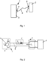
- the device 1 shows a simplified representation of the device 1 according to the invention, to which a test specimen 2 in the form of an electric drive unit is connected.
- the device 1 has a simulation unit 3 for simulating an electrical energy store, for example a battery or an accumulator, and an electrical connecting line 4, at the end of which there is a connecting unit 5 with a plug and/or coupling unit 6.
- screw terminals can also be provided on the connection unit 5 .
- the plug and/or coupling unit 6 is connected to the test object 2 and establishes an electrical connection between the test object 2 and the simulation unit 3 .
- the simulation unit 3 can be formed by a computer or microprocessor and can provide current and voltage via an output 7 according to a simulation model. Current and voltage are transmitted to the test object 2 via the connecting line 4 .
- the simulation unit 3 thus essentially corresponds to a controllable voltage source.
- Such simulation units 3 are also referred to as battery simulators or battery emulators and make it possible to simulate the operation of a test specimen 2 on an energy store. With the help of a simulation model, different operating points of an energy storage device can be simulated without having to use a real energy storage device. The use of a real energy store would represent an enormous effort, since it would first have to be brought to the desired operating point (temperature, charge, etc.). For this reason, simulation units 3 have prevailed for test purposes.
- Modern electrical drive units are often operated on fast-switching converters, i.e. at high (fundamental) frequencies of current and voltage.
- the problem here is that, particularly at high frequencies, the voltage made available to the test object 2 sometimes deviates massively from the voltage at the output 7 of the simulation unit 3 specified by the simulation model.
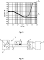
- 2 shows an equivalent circuit diagram of the device 1 according to the invention with a device under test 2 connected to the device 1.
- the connecting line 4 essentially has a resistance covering and an inductance covering, which are shown in 2 can be represented as lumped components R L and L L .
- R L designates the line resistance
- L L the line inductance of the connecting line 4.
- a possible capacitive coating is neglected for the further illustration because of its small influence.
- the actual value of the components R L and L L depends on the geometry of the connecting line 5.
- the expected value of the line resistance R L is in the range of a few m ⁇ , the expected value of the line inductance L L is in the range of a few ⁇ H.
- the simulation unit 3 is shown as a voltage source 8 and has an impedance Z S (shown by a dashed line) which results from the simulation model used or is specified by it.
- the increase in the source impedance Z Q caused by the line inductance L L cannot be corrected by changes in the simulation model. It would be desirable for the source impedance Z Q presented to the test object to correspond to the impedance of the Z S simulation unit. In other words: the influence of the connecting line 4 should be eliminated and the source impedance Z Q should correspond to a default value, for example a general impedance or the impedance Z S of the simulation unit 3 . For this purpose, the impedance Z S of the simulation unit 3 is subsequently also adjusted, ie changed, which is why when the source impedance Z Q should correspond to the impedance Z S of the simulation unit 3, the original impedance Z S of the simulation unit 3 is also discussed.
- a compensation impedance Z K is provided for matching the source impedance Z Q .
- the source impedance Z Q presented to the test specimen 2 can be adapted, ie changed. This should be based on 4 be explained.
- the compensation impedance Z K according to the invention is provided in the connection unit 5. This consists of a compensation capacitor C P and an ohmic compensation resistor R P . Compensation capacitor C P and compensation resistor R P are electrically connected in series. The compensation impedance Z K is electrically connected in parallel with the test object 2 . In order to be able to make adjustments in a simple manner, the compensation capacitor C P and/or the compensation resistor R P can be designed to be adjustable.
- the source impedance Z Q formed from the point of view of the test object 2 is calculated from the parallel connection of the compensation impedance Z K and the series connection from the line impedance Z L and the impedance Z S of the simulation unit 3:
- Z Q s Z S s + R L + sL L R P + 1 sC P
- variable "s" corresponds to the generally complex Laplace variable of the Laplace transform.
- this represents a realizable impedance Z S of the simulation unit 3, which corresponds to a frequency-independent, ohmic resistance.
- the impedance Z S of the simulation unit in Equation 6 corresponds to the preset resistance R S reduced by the line resistance R L .
- the influence of the line inductance can be eliminated by the above selection of the parameters R P and C P and the result is an ohmic resistance value of the impedance Z S of the simulation unit 3 that is particularly easy to form Line resistance R L compensated.
Landscapes
- Physics & Mathematics (AREA)
- General Physics & Mathematics (AREA)
- Engineering & Computer Science (AREA)
- General Engineering & Computer Science (AREA)
- Manufacturing & Machinery (AREA)
- Power Engineering (AREA)
- Health & Medical Sciences (AREA)
- Artificial Intelligence (AREA)
- Evolutionary Computation (AREA)
- Medical Informatics (AREA)
- Measurement Of Resistance Or Impedance (AREA)
- Tests Of Electronic Circuits (AREA)
Description
- Die Erfindung betrifft eine Vorrichtung zum Testen, insbesondere hochfrequenten Testen, eines Prüflings, beispielsweise einer elektrischen Maschine oder eines Umrichters, aufweisend:
- eine Simulationseinheit zur Simulation eines elektrischen Energiespeichers mit Hilfe eines Simulationsmodells und
- eine elektrische Verbindungsleitung, über welche der Prüfling mit der Simulationseinheit verbindbar ist, wobei die Vorrichtung eine Kompensationsimpedanz zur Kompensation einer Impedanz zufolge einer Leitungsinduktivität der Verbindungsleitung aufweist.
- Des Weiteren betrifft die Erfindung ein Verfahren zum Testen, insbesondere hochfrequenten Testen, eines Prüflings, beispielsweise einer elektrischen Maschine oder eines Umrichters, bei dem der Prüfling über eine elektrische Verbindungsleitung mit einer Simulationseinheit verbunden wird, wobei die Simulationseinheit einen elektrischen Energiespeicher mit Hilfe eines Simulationsmodells simuliert, wobei eine Kompensationsimpedanz zur Kompensation einer Impedanz zufolge einer Leitungsinduktivität der Verbindungsleitung verwendet wird.
- Die Spannung an einem Energiespeicher, wie zum Beispiel einer Batterie oder einem Akkumulator, ist nicht konstant, sondern hängt vom Verlauf des aktuellen und des vergangenen Stromflusses, vom Ladezustand, von der Temperatur, von der Alterung des Energiespeichers und von vielen weiteren Dingen ab. Möchte man einen batterie- oder akkubetriebenen Prüfling, zum Beispiel eine elektrische Antriebseinheit eines Fahrzeugs oder einen Umrichter, am Prüfstand realistisch betreiben, könnte man eine reale Batterie verwenden. Der Zeitaufwand, um die Batterie vor jedem Versuch in den gewünschten Zustand (Ladezustand, Temperatur, Alterung usw.) zu bringen wäre allerdings enorm und nicht immer zuverlässig reproduzierbar. Deswegen wird am Prüfstand üblicherweise eine Simulationseinheit, ein sogenannter Batteriesimulator bzw. Batterieemulator, eingesetzt. Die Simulationseinheit stellt grob gesprochen im Wesentlichen eine steuerbare Spannungsquelle dar, die eine vom Simulationsmodell berechnete Spannung ausgibt und dem Prüfling zur Verfügung stellt. Das Simulationsmodell gibt dabei auch die Impedanz der Simulationseinheit vor.
- Um die meist schwere und empfindliche Simulationseinheit nicht bei jeder Prüfung neu platzieren und einrichten zu müssen, wird am Prüfstand in der Regel eine flexible, mehrere Meter lange Verbindungsleitung verwendet. Über diese Verbindungsleitung wird der Prüfling während des Tests mit der Simulationseinheit verbunden und mit Strom bzw. Spannung versorgt.
- Aus dem Stand der Technik sind Batteriesimulatoren unter anderem aus
WO 2013/174967 A1 undDE 296 21 472 U1 bekannt. - Aus dem Artikel "Stabilizing Fast Transient Response Power Supply/Load Circuits", mit der Nummer 2870 aus der Reihe "Application Note Series" von Keithley aus dem Jahr 2007 ist ein Batteriesimulator zum Betreiben bzw. Testen von portablen Geräten bekannt. Um einem Prüfling eine bestimmte Ausgangsspannung zur Verfügung zu stellen, ist eine Regelung mit einer Rückkoppelung über Messleitungen vorgesehen. Es wird beschrieben, dass die Ausgangsspannung des Batteriesimulators aufgrund von Reaktanzen zu oszillieren beginnen und instabil werden kann, wenn transiente Schaltvorgänge auftreten. Zur Erhöhung der Stabilität werden mehrere Methoden vorgeschlagen. Unter anderem kann ein Kompensationsnetzwerk vorgesehen sein. Durch diese Maßnahme soll die Stabilität der Schaltung erhöht werden. Die Kompensationskondensatoren und die Kompensationswiderstände des Kompensationsnetzwerkes schließen den Rückkoppelungskreis und sind damit nicht parallel zum Prüfling angeordnet. Mithilfe des Kompensationsnetzwerks soll ein Bypass für die Leitungsinduktivität und die Kapazität des Rückkoppelungsnetzwerks für Frequenzen f>fres realisiert werden.
- Weitere Energieversorgungsvorrichtungen sind aus
KR 100 652 728 B1 DE 10 2012 217 973 A1 ,DE 10 2011 054 370 A1 und Buccolini Luca et al: "Cell Battery Emulator for Hardware-in-the-Loop BMS Test", 2018 IEEE INTERNATIONAL CONFERENCE ON ENVIRON-MENT AND ELECTRICAL ENGINEERING AND 2018 IEEE INDUSTRIAL AND COMMERCTAL POWER SYSTEMS EUROPE (EEEIC / I&CPS EUROPE), IEEE, 12. Juni 2018 (2018-06-12), Seiten 1-5, bekannt. - Moderne Antriebseinheiten werden häufig an schnell schaltenden Umrichtereinheiten betrieben. Zu Testzwecken werden diese häufig an Prüfständen mit Vorrichtungen der eingangs erwähnten Art getestet. Problematisch ist jedoch, dass insbesondere bei hohen Schaltfrequenzen die dem Prüfling tatsächlich zur Verfügung gestellte Spannung zum Teil beträchtlich von den durch das Simulationsmodell vorgegebenen Spannung abweicht und hochfrequente Spannungsschwankungen auftreten können. Dies kann dazu führen, dass der Prüfling wegen Über- oder Unterspannung abschaltet oder dass der Prüfling beschädigt wird. Eine Kompensation dieser Abweichung durch das Simulationsmodell ist bislang, nicht zuletzt auf Grund der dazu theoretisch notwendig Spannungserhöhung durch die Simulationseinheit, nicht möglich. Tests an schnell schaltenden Prüflingen sind daher nicht zuverlässig durchführbar.
- Es ist daher Aufgabe der vorliegenden Erfindung, die Nachteile des Standes der Technik zu lindern oder gar gänzlich zu beseitigen. Insbesondere ist es Aufgabe der vorliegenden Erfindung, die Abweichungen zwischen der dem Prüfling zur Verfügung gestellten Spannung und der durch das Simulationsmodell vorgegebenen Spannung zu minimieren bzw. zu beseitigen und dadurch eine zuverlässige Prüfung auch bei hohen Schaltfrequenzen der Prüflinge zu ermöglichen.
- Gelöst wird diese Aufgabe in durch die Merkmale des kennzeichnenden Teils des Anspruch 1. Die Vorrichtung zeichnet sich demnach dadurch aus, dass die Kompensationsimpedanz derart angeordnet ist, dass sie in einem angeschlossenen Zustand des Prüflings elektrisch parallel zum Prüfling angeordnet ist.
- Vorteilhafterweise kann mit Hilfe der Kompensationsimpedanz der Einfluss des induktiven, frequenzabhängigen Anteils der Leitungsimpedanz der Verbindungsleitung kompensiert werden, sodass auch bei höheren Frequenzen ein zuverlässiges Testen eines Prüflings an der Vorrichtung ermöglicht wird. "Höhere Frequenzen" bzw. "Hochfrequenz" bedeuten in diesem Zusammenhang Frequenzen der Spannung bzw. des Stroms von zumindest 300 Hz, insbesondere zumindest 1000 Hz, vorzugsweise zumindest 3000 Hz.
- Die Erfindung beruht dabei auf der Erkenntnis, dass Schwankungen in der Spannung und die Abweichungen zwischen den durch das Simulationsmodell vorgegebenen Spannung und der tatsächlich dem Prüfling am Ende der Verbindungsleitung zur Verfügung gestellten Spannung primär auf den Widerstands- und Induktivitätsbelag der Verbindungsleitung zurückzuführen sind. Der kapazitive Belag kann dabei ob seines geringen Einflusses vernachlässigt werden. Der Widerstands- und der Induktivitätsbelag der Verbindungsleitung bilden die Leitungsimpedanz der Verbindungsleitung und führen ohne jegliche Kompensation dazu, dass die vom Prüfling im verbundenen Zustand aus "sichtbare" Quellimpedanz der Vorrichtung erhöht wird und diese daher von der Impedanz der Simulationseinheit abweicht. Die "sichtbare" Quellimpedanz des Prüflings wird dabei durch eine Impedanz der Simulationseinheit und die Leitungsimpedanz der Verbindungleitung gebildet. Je länger dabei die Verbindungsleitung ist, desto größer ist diese Abweichung. Auf Grund der Leitungsinduktivität bzw. der Impedanz zufolge der Leitungsinduktivität erhöht sich mit zunehmender Frequenz der Betrag der Leitungsimpedanz und damit der Betrag der Quellimpedanz. Dies führt, wie oben geschildert, insbesondere bei hohen Frequenzen zu Problemen, da sich dem Prüfling, nicht wie eigentlich gewünscht, die Impedanz der Simulationseinheit, sondern die vergrößerte Quellimpedanz darstellt.
- Durch die erfindungsgemäße Kompensationsimpedanz kann der beschriebenen Problematik entgegengewirkt werden. Insbesondere ist es mit der erfindungsgemäßen Kompensationsimpedanz, wie bereits erwähnt, möglich, durch die Wahl geeigneter Parameter den Einfluss der Leitungsinduktivität der Verbindungsleitung zu minimieren oder gänzlich zu beseitigen. Dies erfolgt dadurch, dass durch die Kompensationsimpedanz die vom Prüfling im verbundenen Zustand sichtbare Quellimpedanz angepasst, d.h. verändert wird. Der Wert der Quellimpedanz kann dabei an einen Vorgabewert angepasst werden, welcher beispielsweise dem Simulationsmodell entstammen kann. Beispielsweise kann die Quellimpedanz derart verändert werden, dass die Quellimpedanz der (ursprünglichen) Impedanz der Simulationseinheit entspricht. Der Einfluss der Verbindungsleitung wird dabei eliminiert. Die Vorrichtung wirkt in diesem Fall für den Prüfling so, als würde er direkt ohne Verbindungsleitung an die Simulationseinheit angeschlossen sein. Mit anderen Worten ist es möglich, durch Verwendung der Kompensationsimpedanz und gegebenenfalls Änderung der ursprünglichen Impedanz der Simulationseinheit eine Quellimpedanz der Vorrichtung einzustellen, die dem ursprünglich gewünschten, durch das Simulationsmodell vorgegebenen Wert der Impedanz der Simulationseinheit entspricht. Falls notwendig oder zweckdienlich, kann auch eine Änderung, insbesondere eine Reduktion, der Impedanz der Simulationseinheit vorgenommen werden.
- Zweckmäßigerweise kann die Kompensationsimpedanz einen ohmschen Anteil und einen kapazitiven Anteil aufweisen. Durch die Kompensationsimpedanz und gegebenenfalls gleichzeitige Änderung, insbesondere Reduktion, der Impedanz der Simulationseinheit kann zum einen der Einfluss des Leitungswiderstandes der Verbindungsleitung, der bereits einer Frequenz von 0 Hz auftritt und über den gesamten Frequenzbereich annähernd konstant ist, und zum anderen der Einfluss der Leitungsinduktivität, die insbesondere bei Frequenzen über 300 Hz an Einfluss gewinnt, kompensiert werden.
- Bei der Simulationseinheit, welche auch als Batteriesimulator oder Batterieemulator bezeichnet wird, kann eine Recheneinheit, wie etwa einen Computer oder eine Mikroprozessoreinheit, aufweisen. Die Recheneinheit ist in der Lage, das Simulationsmodell auszuführen bzw. zu berechnen und eine Spannung und/oder einen Strom gemäß dem Simulationsmodell an einem Ausgang der Simulationseinheit auszugeben. Hierdurch können Netzwerke, bestehend aus Widerständen, Induktivitäten und Kapazitäten rasch nachgebildet werden. Die Simulationseinheit stellt somit eine steuer- bzw. regelbare Spannungsquelle dar. Die Bauteilwerte hängen vom Betriebszustand des simulierten Energiespeichers ab und werden durch das Simulationsmodell vorgegeben. Das Simulationsmodell gibt somit die Impedanz der Simulationseinheit vor. Die Verbindungsleitung ist mit dem Ausgang der Simulationseinheit verbindbar. Als Verbindungsleitung kann ein mehrpoliges Kabel, beispielsweise ein zweipoliges Kabel, vorzugsweise mit geringer Leitungsinduktivität, vorgesehen sein.
- Es ist vorgesehen, dass die Kompensationsimpedanz derart angeordnet ist, dass sie in einem angeschlossenen Zustand des Prüflings elektrisch parallel zum Prüfling angeordnet ist. Dadurch wird ein möglicher negativer Einfluss der Kompensationsimpedanz bei niedrigen Frequenzen vermieden.
- Eine einfache Anpassung der Quellimpedanz ergibt sich, wenn die Kompensationsimpedanz an einem dem Prüfling zugewandten Ende der Verbindungsleitung, vorzugsweise zwischen dem Prüfling zugewandten Ende der Verbindungsleitung und dem Prüfling, insbesondere in einer Verbindungseinheit, angeordnet ist. Durch die Anordnung in der Nähe des Prüflings können die Einflüsse der Verbindungsleitung besonders effizient kompensiert werden. Die Verbindungseinheit kann zumindest eine Schraubklemme, eine Stecker- und/oder Kupplungseinheit aufweisen, mit der der Prüfling direkt verbunden werden kann.
- Zur Erzeugung eines ohmschen und eines kapazitiven Anteils kann die Kompensationsimpedanz einen ohmschen Kompensationswiderstand und einen Kompensationskondensator aufweisen, wobei der Kompensationswiderstand und der Kompensationskondensator vorzugsweise elektrisch in Serie geschaltet sind. Durch den Kompensationskondensator ergibt sich der Vorteil, dass der Einfluss des Kompensationswiderstands auf die Quellimpedanz bei niedrigen Frequenzen gering gehalten werden kann.
- Um Veränderungen des Simulationsmodells und andere Einflüsse, wie etwa Temperaturschwankungen, jederzeit berücksichtigen zu können, kann es vorteilhaft sein, wenn als ohmscher Kompensationswiderstand ein verstellbarer Widerstand und/oder wenn als Kompensationskondensator ein verstellbarer Kondensator vorgesehen ist. Der Kompensationswiderstand und der Kompensationskondensator können dabei beispielsweise mechanisch verstellbar sein. Zum Beispiel kann als Kompensationswiderstand ein Potentiometer vorgesehen sein. Es können aber auch schaltbare Widerstandsnetzwerke für den Kompensationswiderstand bzw. schaltbare Kondensatornetzwerke für den Kompensationskondensator vorgesehen sein. Diese können manuell und/oder elektronisch angesteuert werden.
- In einer besonders bevorzugten Ausführungsform kann vorgesehen sein, die Kompensationsimpedanz eine aus einer Leitungsimpedanz der Verbindungsleitung und der Impedanz der Simulationseinheit gebildete Quellimpedanz derart anpasst, dass die Quellimpedanz einem ohmschen Vorgabewiderstand entspricht. Die vom Prüfling aus sichtbare Quellimpedanz ist demnach (unter Vernachlässigung kapazitiver Anteile) ein rein ohmscher Widerstand. Für den Prüfling wirkt die Vorrichtung also so, als ob er an einen Energiespeicher mit einer ohmschen Quellimpedanz angeschlossen wäre. Zusätzlich kann zweckmäßigerweise auch eine Anpassung, insbesondere eine Reduktion, der Impedanz der Simulationseinheit vorgenommen werden, um die Quellimpedanz zu reduzieren. Bei dem Vorgabewiderstand kann es sich um einen allgemeinen ohmschen Widerstand oder eine ursprünglich durch das Simulationsmodell vorgegebene rein ohmsche Impedanz der Simulationseinheit handeln.
- In einer Ausführungsform kann vorgesehen sein, dass der Wert des Kompensationswiderstands im Wesentlichen dem Wert des Vorgabewiderstands entspricht.
- Vorteilhaft ist dabei, wenn die Impedanz der Simulationseinheit einem ohmschen Innenwiderstand entspricht, der gemäß der Formel RI = RS - RL dimensioniert ist, wobei RS den ohmschen Vorgabewiderstand und RL einen ohmschen Leitungswiderstand der Verbindungsleitung bezeichnet. Hierdurch kann vorteilhafterweise der Leitungswiderstand kompensiert werden.
- Weiters ist es günstig, wenn der Kompensationskondensator gemäß der Formel CP = LL/(RP 2) dimensioniert ist, wobei LL eine Leitungsinduktivität der Verbindungsleitung und RP den Kompensationswiderstand bezeichnet.
- Durch die oben genannte Wahl der Parameter erfolgt auf vorteilhafte Weise eine Anpassung der Quellimpedanz an einen Vorgabewert, und das nicht nur bei einer bestimmten Frequenz, sondern über den gesamten Frequenzbereich. Zusammenfassend kann die Quellimpedanz auf besonders effiziente Weise angepasst werden, wenn die Impedanz der Simulationseinheit RI = RS - RL entspricht, der Kapazitätswert des Kompensationskondensators CP = LL/(RP 2) beträgt und der Wert des Kompensationswiderstands im Wesentlichen dem ohmschen Vorgabewiderstand entspricht. Dann entspricht auch die Quellimpedanz vorteilhafterweise dem Vorgabewiderstand.
- Des Weiteren wird die oben gestellte Aufgabe durch ein Verfahren nach Anspruch 9 gelöst. Bei dem Verfahren ist erfindungsgemäß vorgesehen, dass die Kompensationsimpedanz elektrisch parallel zum Prüfling angeordnet ist.
- Die in Bezug auf die Vorrichtung beschriebenen Vorteile und Merkmale sind uneingeschränkt auch auf das Verfahren anwendbar.
- Im Folgenden wird die Erfindung an Hand von Figuren näher beschrieben, auf die sie allerdings nicht beschränkt sein soll.
-
Fig. 1 zeigt eine vereinfachte Darstellung der erfindungsgemäßen Vorrichtung mit einem an die Vorrichtung angeschlossenen Prüfling. -
Fig. 2 zeigt ein Ersatzschaltbild der erfindungsgemäßen Vorrichtung mit einem an die Vorrichtung angeschlossenen Prüfling. -
Fig. 3 zeigt einen Amplitudengang der Quellimpedanz ohne Kompensation und den Amplitudengang der Impedanz der Simulationseinheit. -
Fig. 4 zeigt ein Ersatzschaltbild der erfindungsgemäßen Vorrichtung mit einem an die Vorrichtung angeschlossenen Prüfling und einer Kompensationsimpedanz ZK. -
Fig. 1 zeigt eine vereinfachte Darstellung der erfindungsgemäßen Vorrichtung 1, an welche ein Prüfling 2 in Form einer elektrischen Antriebseinheit angeschlossen ist. Die Vorrichtung 1 weist eine Simulationseinheit 3 zur Simulation eines elektrischen Energiespeichers, beispielsweise einer Batterie oder eines Akkumulators, und eine elektrische Verbindungsleitung 4 auf, an deren Ende sich eine Verbindungseinheit 5 mit einer Stecker- und/oder Kupplungseinheit 6 befindet. Es können aber auch Schraubklemmen an der Verbindungseinheit 5 vorgesehen sein. Die Stecker- und/oder Kupplungseinheit 6 ist an den Prüfling 2 angeschlossen und stellt eine elektrische Verbindung zwischen dem Prüfling 2 und der Simulationseinheit 3 her. - Die Simulationseinheit 3 kann durch einen Computer oder Mikroprozessor gebildet sein und über einen Ausgang 7 Strom- und Spannung gemäß einem Simulationsmodell zur Verfügung stellen. Strom und Spannung wird über die Verbindungsleitung 4 an den Prüfling 2 übertragen. Die Simulationseinheit 3 entspricht somit im Wesentlichen einer steuerbaren Spannungsquelle.
- Derartige Simulationseinheiten 3 werden auch als Batteriesimulatoren oder Batterieemulatoren bezeichnet und ermöglichen es, den Betrieb eines Prüflings 2 an einem Energiespeicher zu simulieren. Mit Hilfe eines Simulationsmodells können unterschiedliche Betriebspunkte eines Energiespeichers simuliert werden, ohne dass ein realer Energiespeicher verwendet werden muss. Die Verwendung eines realen Energiespeichers würde einen enormen Aufwand darstellen, da dieser zunächst in den gewünschten Betriebspunkt (Temperatur, Ladung etc.) gebracht werden müsste. Aus diesem Grund haben sich Simulationseinheiten 3 für Testzwecke durchgesetzt.
- Vielfach werden moderne elektrische Antriebseinheiten an schnell schaltenden Umrichtern, d.h. bei hohen (Grund-)Frequenzen von Strom und Spannung, betrieben. Problematisch ist dabei jedoch, dass insbesondere bei hohen Frequenzen die dem Prüfling 2 zur Verfügung gestellte Spannung von der durch das Simulationsmodell vorgegebenen Spannung am Ausgang 7 der Simulationseinheit 3 mitunter massiv abweicht.
- Für dieses Problem konnte folgende Ursache identifiziert werden, die an Hand der
Figuren 2 und3 veranschaulicht werden soll:
Fig. 2 zeigt ein Ersatzschaltbild der erfindungsgemäßen Vorrichtung 1 mit einem an die Vorrichtung 1 angeschlossenen Prüfling 2. Die Verbindungsleitung 4 weist im Wesentlichen einen Widerstandsbelag und einen Induktivitätsbelag auf, welche inFig. 2 als konzentrierte Bauteile RL und LL dargestellt werden. Dabei bezeichnet RL den Leitungswiderstand und LL die Leitungsinduktivität der Verbindungsleitung 4. Ein allfälliger kapazitiver Belag wird für die weitere Veranschaulichung ob seines geringen Einflusses vernachlässigt. Der tatsächliche Wert der Bauteile RL und LL hängt von der Geometrie der Verbindungsleitung 5 ab. Der erwartbare Wert des Leitungswiderstands RL liegt im Bereich von einigen mQ, der erwartbare Wert der Leitungsinduktivität LL liegt im Bereich von einigen µH. Der Leitungswiderstand RL und die Leitungsinduktivität LL bilden zusammen (unter Vernachlässigung des kapazitiven Anteils) eine Leitungsimpedanz ZL. Die Simulationseinheit 3 ist als Spannungsquelle 8 dargestellt und weist eine (durch eine gestrichelte Linie dargestellte) Impedanz ZS auf, welche sich aus dem verwendeten Simulationsmodell ergibt bzw. von diesem vorgegeben wird. - Der Widerstandsbelag und der Induktivitätsbelag haben nun eine Auswirkung auf die Impedanz der Vorrichtung 1, die der Prüfling "sieht". Diese Impedanz wird als Quellimpedanz ZQ bezeichnet und setzt sich zunächst im Wesentlichen aus der Impedanz ZS der Simulationseinheit 3 und der Leitungsimpedanz ZL zusammen. Durch den Widerstandsbelag und den Induktivitätsbelag weicht die vom Prüfling "gesehene" Quellimpedanz ZQ von der Impedanz ZS der Simulationseinheit 3, insbesondere bei Frequenzen >300 Hz, ab. Dies ist in
Fig. 3 ersichtlich, welche den Amplitudengang in dB der sich dem Prüfling 2 darstellenden Quellimpedanz ZQ (gestrichelte Linie) und den Amplitudengang der Impedanz ZS der Simulationseinheit 3 (durchgezogene Linie) abbildet. Hierbei können zwei Phänomene beobachtet werden: - 1) Bei niedrigen Frequenzen ist die Quellimpedanz ZQ leicht erhöht. Dies wird durch den Leitungswiderstand RL verursacht, der im Wesentlichen über alle Frequenzen konstant ist.
- 2) Bei hohen Frequenzen steigt die Quellimpedanz ZQ stark an. Dies wird als hochfrequente Trennung zwischen Simulationseinheit 3 und Prüfling 2 bezeichnet und wird primär durch die Leitungsinduktivität LL verursacht.
- Der durch die Leitungsinduktivität LL verursachte Anstieg der Quellimpedanz ZQ kann nicht durch Änderungen im Simulationsmodell korrigiert werden. Wünschenswert wäre, dass die sich dem Prüfling darstellende Quellimpedanz ZQ der Impedanz der ZS Simulationseinheit entspricht. Mit anderen Worten: Der Einfluss der Verbindungsleitung 4 soll eliminiert werden und die Quellimpedanz ZQ soll einem Vorgabewert, beispielsweise einer allgemeinen Impedanz oder der Impedanz ZS der Simulationseinheit 3, entsprechen. Zu diesem Zweck wird in weiterer Folge auch die Impedanz ZS der Simulationseinheit 3 angepasst, d.h. verändert, weshalb, wenn die Quellimpedanz ZQ der Impedanz ZS der Simulationseinheit 3 entsprechen soll, auch von der ursprünglichen Impedanz ZS der Simulationseinheit 3 die Rede ist.
- Erfindungsgemäß ist eine Kompensationsimpedanz ZK zur Anpassung der Quellimpedanz ZQ vorgesehen. Mit Hilfe der Kompensationsimpedanz ZK kann die sich dem Prüfling 2 darstellende Quellimpedanz ZQ angepasst, d.h. verändert werden. Dies soll an Hand von
Fig. 4 erläutert werden. -
Fig. 4 zeigt erneut ein Ersatzschaltbild der erfindungsgemäßen Vorrichtung 1 mit einem angeschlossenen Prüfling 2. In der Verbindungseinheit 5 ist jedoch die erfindungsgemäße Kompensationsimpedanz ZK vorgesehen. Diese besteht aus einem Kompensationskondensator CP und einem ohmschen Kompensationswiderstand RP. Der Kompensationskondensator CP und der Kompensationswiderstand RP sind elektrisch in Serie geschaltet. Die Kompensationsimpedanz ZK ist elektrisch parallel zum Prüfling 2 geschaltet. Um auf einfache Weise Anpassungen vornehmen zu können, können der Kompensationskondensator CP und/oder der Kompensationswiderstand RP verstellbar ausgebildet sein. - Die aus Sicht des Prüflings 2 gebildete Quellimpedanz ZQ berechnet sich aus der Parallelschaltung der Kompensationsimpedanz ZK und der Serienschaltung aus der Leitungsimpedanz ZL und der Impedanz ZS der Simulationseinheit 3:

- Die Variable "s" entspricht hierbei der im allgemeinen komplexen Laplace Variable der Laplace-Transformation. Zur Verdeutlichung, dass es sich bei den Impedanzen ZQ und ZS um allgemeine, frequenzabhängige Impedanzen handeln kann, wurde diesen Impedanzen in den Gleichungen die Variable (s) beigefügt. Soll die Quellimpedanz ZQ einem Vorgabewert ZSOLL entsprechen, muss gelten:


- Es soll nun vereinfacht vorgesehen sein, dass die Quellimpedanz ZQ einem konstanten ohmschen Vorgabewiderstand ZSOLL = RS entsprechen soll. Der Vorgabewiderstand RS kann beispielsweise jener Wert sein, den das Simulationsmodell für den Prüfling 2 vorgesehen hätte, jedoch auf Grund der Verbindungsleitung 4 verfälscht werden würde. Gleichung 3 lässt sich unter dieser Vorgabe wie folgt umformen:

- Auf Grund des höheren Zählergrades (siehe die Laplace Variable s) in Gleichung 4 handelt es sich hierbei um eine nicht realisierbare Impedanz ZS. Wenn nun für RP = RS gewählt wird, erhält man

- was allerdings eine noch immer nicht realisierbare Impedanz darstellt. Durch die Wahl


- Dies stellt schließlich eine realisierbare Impedanz ZS der Simulationseinheit 3 dar, welche einem frequenzunabhängigen, ohmschen Widerstand entspricht. Die Impedanz ZS der Simulationseinheit in Gleichung 6 entspricht dabei dem um den Leitungswiderstand RL reduzierten Vorgabewiderstand RS. Durch die obige Wahl der Parameter RP und CP kann also der Einfluss der Leitungsinduktivität eliminiert werden und es ergibt sich ein besonders einfach zu bildender ohmscher Widerstandswert der Impedanz ZS der Simulationseinheit 3. Durch die Subtraktion RL von RS wird dabei der ohmsche Leitungswiderstand RL kompensiert.
- Die obigen Annahmen und Ergebnisse dienen als Ausführungsbeispiel und können wie folgt zusammengefasst und interpretiert werden: Um die Quellimpedanz ZQ der Vorrichtung, welche sich dem Prüfling 2 darstellt, derart zu verändern, dass sie einer einem vorgegebenen ohmschen Widerstandswert RS entspricht, ist es günstig, wenn die Impedanz ZS der Simulationseinheit 3 dem Widerstandswert RS - RL entspricht. Anders formuliert: Die Impedanz ZS der Simulationseinheit soll dem um den Leitungswiderstand RL reduzierten Vorgabewiderstand RS entsprechen. Des Weiteren soll die Kapazität des Kompensationskondensator CP nach Gleichung 6 gewählt werden und der Kompensationswiderstand RP dem Vorgabewiderstand RS entsprechen.
Claims (9)
- Vorrichtung (1) zum Testen, insbesondere hochfrequenten Testen, eines Prüflings (2), beispielsweise einer elektrischen Maschine oder eines Umrichters, aufweisend:- eine Simulationseinheit (3) zur Simulation eines elektrischen Energiespeichers mit Hilfe eines Simulationsmodells und- eine elektrische Verbindungsleitung (4), über welche der Prüfling (2) mit der Simulationseinheit (3) verbindbar ist,wobei die Vorrichtung (1) eine Kompensationsimpedanz (ZK) zur Kompensation einer Impedanz zufolge einer Leitungsinduktivität (LL) der Verbindungsleitung (4) aufweist, dadurch gekennzeichnet, dass die Kompensationsimpedanz (ZK) derart angeordnet ist, dass sie in einem angeschlossenen Zustand des Prüflings elektrisch parallel zum Prüfling (2) angeordnet ist.
- Vorrichtung (1) nach Anspruch 1, dadurch gekennzeichnet, dass die Kompensationsimpedanz (ZK) an einem dem Prüfling (2) zugewandten Ende der Verbindungsleitung (4), vorzugsweise zwischen dem Prüfling (2) zugewandten Ende der Verbindungsleitung (4) und dem Prüfling (2), insbesondere in einer Verbindungseinheit (5), angeordnet ist.
- Vorrichtung (1) nach einem der Ansprüche 1 oder 2, dadurch gekennzeichnet, dass die Kompensationsimpedanz (ZK) einen ohmschen Kompensationswiderstand (RP) und einen Kompensationskondensator (CP) aufweist, wobei der Kompensationswiderstand (RP) und der Kompensationskondensator (CP) vorzugsweise elektrisch in Serie geschaltet sind.
- Vorrichtung (1) nach Anspruch 3, dadurch gekennzeichnet, dass als Kompensationswiderstand (RP) ein verstellbarer Widerstand und/oder dass als Kompensationskondensator (CP) ein verstellbarer Kondensator vorgesehen sind/ist.
- Vorrichtung (1) nach einem der Ansprüche 3 oder 4, dadurch gekennzeichnet, dass die Kompensationsimpedanz (ZK) eine aus einer Leitungsimpedanz (ZL) der Verbindungsleitung (4) und einer Impedanz (ZS) der Simulationseinheit (3) gebildete Quellimpedanz (ZQ) derart anpasst, dass die Quellimpedanz (ZQ) einem ohmschen Vorgabewiderstand (RS) entspricht.
- Vorrichtung (1) nach Anspruch 5, dadurch gekennzeichnet, dass der Wert des Kompensationswiderstands (RP) im Wesentlichen dem Wert des Vorgabewiderstands (RS) entspricht.
- Vorrichtung (1) nach Anspruch 6, dadurch gekennzeichnet, dass die Impedanz (ZS) der Simulationseinheit (3) einem ohmschen Innenwiderstand (RI) entspricht, der gemäß der Formel RI = RS - RL dimensioniert ist, wobei RS den ohmschen Vorgabewiderstand und RL einen ohmschen Leitungswiderstand der Verbindungsleitung (4) bezeichnet.
- Vorrichtung (1) nach einem der Ansprüche 3 bis 7, dadurch gekennzeichnet, dass der Kompensationskondensator (CP) gemäß der Formel CP = LL/(RP 2) dimensioniert ist, wobei LL eine Leitungsinduktivität der Verbindungsleitung (4) und RP den Kompensationswiderstand bezeichnet.
- Verfahren zum Testen, insbesondere hochfrequenten Testen, eines Prüflings (2), beispielsweise einer elektrischen Maschine oder eines Umrichters, bei dem der Prüfling (2) über eine elektrische Verbindungsleitung (4) mit einer Simulationseinheit (3) verbunden wird, wobei die Simulationseinheit (3) einen elektrischen Energiespeicher mit Hilfe eines Simulationsmodells simuliert, wobei eine Kompensationsimpedanz (ZK) zur Kompensation einer Impedanz zufolge einer Leitungsinduktivität (LL) der Verbindungsleitung (4) verwendet wird, dadurch gekennzeichnet, dass die Kompensationsimpedanz (ZK) elektrisch parallel zum Prüfling (2) angeordnet ist.
Applications Claiming Priority (2)
| Application Number | Priority Date | Filing Date | Title |
|---|---|---|---|
| ATA50401/2019A AT522527A1 (de) | 2019-05-03 | 2019-05-03 | Batteriesimulator mit Kompensationsimpedanz |
| PCT/AT2020/060174 WO2020223748A1 (de) | 2019-05-03 | 2020-04-30 | Batteriesimulator mit kompensationsimpedanz |
Publications (2)
| Publication Number | Publication Date |
|---|---|
| EP3963349A1 EP3963349A1 (de) | 2022-03-09 |
| EP3963349B1 true EP3963349B1 (de) | 2022-10-26 |
Family
ID=71083318
Family Applications (1)
| Application Number | Title | Priority Date | Filing Date |
|---|---|---|---|
| EP20732094.6A Active EP3963349B1 (de) | 2019-05-03 | 2020-04-30 | Batteriesimulator mit kompensationsimpedanz |
Country Status (4)
| Country | Link |
|---|---|
| US (1) | US11828808B2 (de) |
| EP (1) | EP3963349B1 (de) |
| AT (1) | AT522527A1 (de) |
| WO (1) | WO2020223748A1 (de) |
Families Citing this family (1)
| Publication number | Priority date | Publication date | Assignee | Title |
|---|---|---|---|---|
| DE102023111363A1 (de) * | 2023-05-03 | 2024-11-07 | Bayerische Motoren Werke Aktiengesellschaft | Verfahren zum Bestimmen einer Korrektur für eine fahrzeugseitige Schätzung eines Zellzustands, Verfahren zum fahrzeugseitigen Schätzen eines Zellzustands, Computerprogramm und/oder computerlesbares Medium, Datenverarbeitungsvorrichtung, Kraftfahrzeug |
Family Cites Families (11)
| Publication number | Priority date | Publication date | Assignee | Title |
|---|---|---|---|---|
| DE29621472U1 (de) | 1996-02-03 | 1997-03-13 | Mack, Helmut, 72764 Reutlingen | Batteriesimulator |
| KR100652728B1 (ko) * | 2005-06-22 | 2006-12-01 | 엘지전자 주식회사 | 지에스엠 방식 이동 통신 단말기의 전원 공급용 커넥터장치 |
| KR100812073B1 (ko) * | 2006-11-09 | 2008-03-07 | 삼성에스디아이 주식회사 | 차동 신호 전송 시스템 및 이를 구비한 평판표시장치 |
| CN102467091B (zh) * | 2010-11-11 | 2017-03-01 | 帝斯贝思数字信号处理和控制工程有限公司 | 具有故障仿真的电池模拟设备及方法 |
| US9143112B2 (en) * | 2011-06-30 | 2015-09-22 | Silicon Laboratories Inc. | Circuits and methods for providing an impedance adjustment |
| AT511520B1 (de) | 2012-05-24 | 2017-06-15 | Avl List Gmbh | Verfahren und eine Vorrichtung zur Prüfung des Antriebsstranges von zumindest teilweise elektrisch betriebenen Fahrzeugen |
| DE102012217973A1 (de) * | 2012-10-02 | 2014-04-03 | Robert Bosch Gmbh | Vorrichtung mit mindestens einer Teilvorrichtung umfassend eine regelbare Spannungsquelle und ein Regelungsmittel und System mit einer solchen Vorrichtung und mit einem Kabelbaum |
| CN203101562U (zh) * | 2013-03-26 | 2013-07-31 | 贾卓 | 电动汽车dc/dc滤波器一体化检测平台 |
| AT513676B1 (de) * | 2014-03-14 | 2018-10-15 | Avl List Gmbh | Energiespeicheremulator und Verfahren zur Emulation eines Energiespeichers |
| US9784780B2 (en) * | 2014-03-24 | 2017-10-10 | Ford Global Technologies, Llc | Battery simulator with variable current capacity |
| CN107592138A (zh) * | 2017-09-26 | 2018-01-16 | 江苏和升智能科技有限公司 | 一种电力线自适应阻抗匹配方法 |
-
2019
- 2019-05-03 AT ATA50401/2019A patent/AT522527A1/de not_active Application Discontinuation
-
2020
- 2020-04-30 US US17/432,053 patent/US11828808B2/en active Active
- 2020-04-30 EP EP20732094.6A patent/EP3963349B1/de active Active
- 2020-04-30 WO PCT/AT2020/060174 patent/WO2020223748A1/de not_active Ceased
Also Published As
| Publication number | Publication date |
|---|---|
| US11828808B2 (en) | 2023-11-28 |
| AT522527A1 (de) | 2020-11-15 |
| EP3963349A1 (de) | 2022-03-09 |
| US20220196742A1 (en) | 2022-06-23 |
| WO2020223748A1 (de) | 2020-11-12 |
Similar Documents
| Publication | Publication Date | Title |
|---|---|---|
| DE102010014070B4 (de) | Verfahren und Prüfstand zum Prüfen von Hybrid-Antriebssystemen oder Teilkomponenten davon | |
| EP1398644A1 (de) | Verfahren zum Testen eines Transformators und entsprechende Testvorrichtung | |
| DE102010062838A1 (de) | Echtzeitfähige Batteriezellensimulation | |
| DE102012211678A1 (de) | System und Verfahren zum Schweißen eines Werkstücks | |
| DE102016105831A1 (de) | Stromversorgungsvorrichtung und Verfahren zur Bereitstellung von Strom für ein elektronisches Gerät, um eine Überlastung wegen elektrischer Entladung zu verhindern | |
| EP3696557A1 (de) | Verfahren und geräte zur bestimmung der elemente eines dielektrischen ersatzschaltbildes für eine isolierung eines elektrischen systems | |
| DE102008036767A1 (de) | Halbleitervorrichtung | |
| WO2016023686A1 (de) | Simulationsvorrichtung und verfahren zur simulation einer an ein regelungsgerät anschliessbaren peripheren schaltungsanordnung | |
| EP3669199B1 (de) | Vorrichtung und verfahren zum kalibrieren eines batteriesimulators | |
| EP3308179B1 (de) | Schaltvorrichtung, testvorrichtung und verfahren zum betreiben einer schaltvorrichtung für ein messgerät für einen transformator | |
| DE102019212782B3 (de) | Verfahren und Vorrichtung zum Bereitstellen eines Verhaltensmodells für die Simulation von elektromagnetischen Störemissionen einer elektrischen bzw. elektronischen Komponente. Verfahren und Simulationsvorrichtung zur Simulation einer Komponente anhand eines der Komponente zugeordneten Verhaltensmodells, Computerprogramm sowie maschinenlesbares Speichermedium | |
| DE102010012688A1 (de) | Schaltanordnung mit Temperaturkompensation | |
| DE102022111267A1 (de) | Computerimplementiertes Verfahren zur Simulation eines elektrischen Antriebs | |
| WO2020223748A1 (de) | Batteriesimulator mit kompensationsimpedanz | |
| EP3786650A1 (de) | Verfahren und vorrichtung zum bereitstellen eines verhaltensmodells für die simulation von elektromagnetischen störemissionen einer elektrischen bzw. elektronischen komponente | |
| DE69224179T2 (de) | Steuerung eines versorgungsnetzes | |
| DE29621472U1 (de) | Batteriesimulator | |
| DE202012001061U1 (de) | Testeinrichtung zum Erzeugen einer Überspannung | |
| DE102022133309A1 (de) | Testanordnung und verfahren zur emulation der phasen-ströme eines elektromotors für ein prüfen eines leistungs-elektronischen steuergeräts | |
| DE102021133994A1 (de) | Vorrichtung und Verfahren zum Kalibrieren eines Batterieemulators | |
| EP3786651B1 (de) | Verfahren und vorrichtung zum bereitstellen eines verhaltensmodells für die simulation von elektromagnetischen störemissionen einer elektrischen bzw. elektronischen komponente | |
| EP4202452B1 (de) | Vorrichtung und verfahren zum kalibrieren eines batterieemulators | |
| DE102020117178A1 (de) | Verfahren zur Analyse von Betriebsparametern eines zu testenden Mobilfunkgeräts sowie Analysesystem | |
| DE10228351A1 (de) | Verfahren und Vorrichtung zur Bestimmung des Alterungszustandes einer Batterie | |
| DE1538609B2 (de) | Transistorisierte Schaltungsanordnung zum automatischen Prüfen gedruckter Leitungszüge |
Legal Events
| Date | Code | Title | Description |
|---|---|---|---|
| STAA | Information on the status of an ep patent application or granted ep patent |
Free format text: STATUS: UNKNOWN |
|
| STAA | Information on the status of an ep patent application or granted ep patent |
Free format text: STATUS: THE INTERNATIONAL PUBLICATION HAS BEEN MADE |
|
| PUAI | Public reference made under article 153(3) epc to a published international application that has entered the european phase |
Free format text: ORIGINAL CODE: 0009012 |
|
| STAA | Information on the status of an ep patent application or granted ep patent |
Free format text: STATUS: REQUEST FOR EXAMINATION WAS MADE |
|
| 17P | Request for examination filed |
Effective date: 20211124 |
|
| AK | Designated contracting states |
Kind code of ref document: A1 Designated state(s): AL AT BE BG CH CY CZ DE DK EE ES FI FR GB GR HR HU IE IS IT LI LT LU LV MC MK MT NL NO PL PT RO RS SE SI SK SM TR |
|
| GRAP | Despatch of communication of intention to grant a patent |
Free format text: ORIGINAL CODE: EPIDOSNIGR1 |
|
| STAA | Information on the status of an ep patent application or granted ep patent |
Free format text: STATUS: GRANT OF PATENT IS INTENDED |
|
| INTG | Intention to grant announced |
Effective date: 20220622 |
|
| DAV | Request for validation of the european patent (deleted) | ||
| DAX | Request for extension of the european patent (deleted) | ||
| GRAS | Grant fee paid |
Free format text: ORIGINAL CODE: EPIDOSNIGR3 |
|
| GRAA | (expected) grant |
Free format text: ORIGINAL CODE: 0009210 |
|
| STAA | Information on the status of an ep patent application or granted ep patent |
Free format text: STATUS: THE PATENT HAS BEEN GRANTED |
|
| AK | Designated contracting states |
Kind code of ref document: B1 Designated state(s): AL AT BE BG CH CY CZ DE DK EE ES FI FR GB GR HR HU IE IS IT LI LT LU LV MC MK MT NL NO PL PT RO RS SE SI SK SM TR |
|
| REG | Reference to a national code |
Ref country code: GB Ref legal event code: FG4D Free format text: NOT ENGLISH |
|
| REG | Reference to a national code |
Ref country code: CH Ref legal event code: EP |
|
| REG | Reference to a national code |
Ref country code: DE Ref legal event code: R096 Ref document number: 502020001899 Country of ref document: DE |
|
| REG | Reference to a national code |
Ref country code: AT Ref legal event code: REF Ref document number: 1527399 Country of ref document: AT Kind code of ref document: T Effective date: 20221115 |
|
| REG | Reference to a national code |
Ref country code: IE Ref legal event code: FG4D Free format text: LANGUAGE OF EP DOCUMENT: GERMAN |
|
| REG | Reference to a national code |
Ref country code: LT Ref legal event code: MG9D |
|
| REG | Reference to a national code |
Ref country code: NL Ref legal event code: MP Effective date: 20221026 |
|
| PG25 | Lapsed in a contracting state [announced via postgrant information from national office to epo] |
Ref country code: NL Free format text: LAPSE BECAUSE OF FAILURE TO SUBMIT A TRANSLATION OF THE DESCRIPTION OR TO PAY THE FEE WITHIN THE PRESCRIBED TIME-LIMIT Effective date: 20221026 |
|
| PG25 | Lapsed in a contracting state [announced via postgrant information from national office to epo] |
Ref country code: SE Free format text: LAPSE BECAUSE OF FAILURE TO SUBMIT A TRANSLATION OF THE DESCRIPTION OR TO PAY THE FEE WITHIN THE PRESCRIBED TIME-LIMIT Effective date: 20221026 Ref country code: PT Free format text: LAPSE BECAUSE OF FAILURE TO SUBMIT A TRANSLATION OF THE DESCRIPTION OR TO PAY THE FEE WITHIN THE PRESCRIBED TIME-LIMIT Effective date: 20230227 Ref country code: NO Free format text: LAPSE BECAUSE OF FAILURE TO SUBMIT A TRANSLATION OF THE DESCRIPTION OR TO PAY THE FEE WITHIN THE PRESCRIBED TIME-LIMIT Effective date: 20230126 Ref country code: LT Free format text: LAPSE BECAUSE OF FAILURE TO SUBMIT A TRANSLATION OF THE DESCRIPTION OR TO PAY THE FEE WITHIN THE PRESCRIBED TIME-LIMIT Effective date: 20221026 Ref country code: FI Free format text: LAPSE BECAUSE OF FAILURE TO SUBMIT A TRANSLATION OF THE DESCRIPTION OR TO PAY THE FEE WITHIN THE PRESCRIBED TIME-LIMIT Effective date: 20221026 Ref country code: ES Free format text: LAPSE BECAUSE OF FAILURE TO SUBMIT A TRANSLATION OF THE DESCRIPTION OR TO PAY THE FEE WITHIN THE PRESCRIBED TIME-LIMIT Effective date: 20221026 |
|
| PG25 | Lapsed in a contracting state [announced via postgrant information from national office to epo] |
Ref country code: RS Free format text: LAPSE BECAUSE OF FAILURE TO SUBMIT A TRANSLATION OF THE DESCRIPTION OR TO PAY THE FEE WITHIN THE PRESCRIBED TIME-LIMIT Effective date: 20221026 Ref country code: PL Free format text: LAPSE BECAUSE OF FAILURE TO SUBMIT A TRANSLATION OF THE DESCRIPTION OR TO PAY THE FEE WITHIN THE PRESCRIBED TIME-LIMIT Effective date: 20221026 Ref country code: LV Free format text: LAPSE BECAUSE OF FAILURE TO SUBMIT A TRANSLATION OF THE DESCRIPTION OR TO PAY THE FEE WITHIN THE PRESCRIBED TIME-LIMIT Effective date: 20221026 Ref country code: IS Free format text: LAPSE BECAUSE OF FAILURE TO SUBMIT A TRANSLATION OF THE DESCRIPTION OR TO PAY THE FEE WITHIN THE PRESCRIBED TIME-LIMIT Effective date: 20230226 Ref country code: HR Free format text: LAPSE BECAUSE OF FAILURE TO SUBMIT A TRANSLATION OF THE DESCRIPTION OR TO PAY THE FEE WITHIN THE PRESCRIBED TIME-LIMIT Effective date: 20221026 Ref country code: GR Free format text: LAPSE BECAUSE OF FAILURE TO SUBMIT A TRANSLATION OF THE DESCRIPTION OR TO PAY THE FEE WITHIN THE PRESCRIBED TIME-LIMIT Effective date: 20230127 |
|
| REG | Reference to a national code |
Ref country code: DE Ref legal event code: R097 Ref document number: 502020001899 Country of ref document: DE |
|
| PG25 | Lapsed in a contracting state [announced via postgrant information from national office to epo] |
Ref country code: SM Free format text: LAPSE BECAUSE OF FAILURE TO SUBMIT A TRANSLATION OF THE DESCRIPTION OR TO PAY THE FEE WITHIN THE PRESCRIBED TIME-LIMIT Effective date: 20221026 Ref country code: RO Free format text: LAPSE BECAUSE OF FAILURE TO SUBMIT A TRANSLATION OF THE DESCRIPTION OR TO PAY THE FEE WITHIN THE PRESCRIBED TIME-LIMIT Effective date: 20221026 Ref country code: EE Free format text: LAPSE BECAUSE OF FAILURE TO SUBMIT A TRANSLATION OF THE DESCRIPTION OR TO PAY THE FEE WITHIN THE PRESCRIBED TIME-LIMIT Effective date: 20221026 Ref country code: DK Free format text: LAPSE BECAUSE OF FAILURE TO SUBMIT A TRANSLATION OF THE DESCRIPTION OR TO PAY THE FEE WITHIN THE PRESCRIBED TIME-LIMIT Effective date: 20221026 Ref country code: CZ Free format text: LAPSE BECAUSE OF FAILURE TO SUBMIT A TRANSLATION OF THE DESCRIPTION OR TO PAY THE FEE WITHIN THE PRESCRIBED TIME-LIMIT Effective date: 20221026 |
|
| PG25 | Lapsed in a contracting state [announced via postgrant information from national office to epo] |
Ref country code: SK Free format text: LAPSE BECAUSE OF FAILURE TO SUBMIT A TRANSLATION OF THE DESCRIPTION OR TO PAY THE FEE WITHIN THE PRESCRIBED TIME-LIMIT Effective date: 20221026 Ref country code: AL Free format text: LAPSE BECAUSE OF FAILURE TO SUBMIT A TRANSLATION OF THE DESCRIPTION OR TO PAY THE FEE WITHIN THE PRESCRIBED TIME-LIMIT Effective date: 20221026 |
|
| PLBE | No opposition filed within time limit |
Free format text: ORIGINAL CODE: 0009261 |
|
| STAA | Information on the status of an ep patent application or granted ep patent |
Free format text: STATUS: NO OPPOSITION FILED WITHIN TIME LIMIT |
|
| 26N | No opposition filed |
Effective date: 20230727 |
|
| PG25 | Lapsed in a contracting state [announced via postgrant information from national office to epo] |
Ref country code: SI Free format text: LAPSE BECAUSE OF FAILURE TO SUBMIT A TRANSLATION OF THE DESCRIPTION OR TO PAY THE FEE WITHIN THE PRESCRIBED TIME-LIMIT Effective date: 20221026 |
|
| REG | Reference to a national code |
Ref country code: CH Ref legal event code: PL |
|
| PG25 | Lapsed in a contracting state [announced via postgrant information from national office to epo] |
Ref country code: LU Free format text: LAPSE BECAUSE OF NON-PAYMENT OF DUE FEES Effective date: 20230430 |
|
| REG | Reference to a national code |
Ref country code: BE Ref legal event code: MM Effective date: 20230430 |
|
| PG25 | Lapsed in a contracting state [announced via postgrant information from national office to epo] |
Ref country code: MC Free format text: LAPSE BECAUSE OF FAILURE TO SUBMIT A TRANSLATION OF THE DESCRIPTION OR TO PAY THE FEE WITHIN THE PRESCRIBED TIME-LIMIT Effective date: 20221026 |
|
| PG25 | Lapsed in a contracting state [announced via postgrant information from national office to epo] |
Ref country code: MC Free format text: LAPSE BECAUSE OF FAILURE TO SUBMIT A TRANSLATION OF THE DESCRIPTION OR TO PAY THE FEE WITHIN THE PRESCRIBED TIME-LIMIT Effective date: 20221026 Ref country code: LI Free format text: LAPSE BECAUSE OF NON-PAYMENT OF DUE FEES Effective date: 20230430 Ref country code: CH Free format text: LAPSE BECAUSE OF NON-PAYMENT OF DUE FEES Effective date: 20230430 |
|
| REG | Reference to a national code |
Ref country code: IE Ref legal event code: MM4A |
|
| PG25 | Lapsed in a contracting state [announced via postgrant information from national office to epo] |
Ref country code: BE Free format text: LAPSE BECAUSE OF NON-PAYMENT OF DUE FEES Effective date: 20230430 |
|
| PG25 | Lapsed in a contracting state [announced via postgrant information from national office to epo] |
Ref country code: IE Free format text: LAPSE BECAUSE OF NON-PAYMENT OF DUE FEES Effective date: 20230430 |
|
| PG25 | Lapsed in a contracting state [announced via postgrant information from national office to epo] |
Ref country code: IE Free format text: LAPSE BECAUSE OF NON-PAYMENT OF DUE FEES Effective date: 20230430 |
|
| PG25 | Lapsed in a contracting state [announced via postgrant information from national office to epo] |
Ref country code: IT Free format text: LAPSE BECAUSE OF FAILURE TO SUBMIT A TRANSLATION OF THE DESCRIPTION OR TO PAY THE FEE WITHIN THE PRESCRIBED TIME-LIMIT Effective date: 20221026 |
|
| PG25 | Lapsed in a contracting state [announced via postgrant information from national office to epo] |
Ref country code: BG Free format text: LAPSE BECAUSE OF FAILURE TO SUBMIT A TRANSLATION OF THE DESCRIPTION OR TO PAY THE FEE WITHIN THE PRESCRIBED TIME-LIMIT Effective date: 20221026 |
|
| PG25 | Lapsed in a contracting state [announced via postgrant information from national office to epo] |
Ref country code: BG Free format text: LAPSE BECAUSE OF FAILURE TO SUBMIT A TRANSLATION OF THE DESCRIPTION OR TO PAY THE FEE WITHIN THE PRESCRIBED TIME-LIMIT Effective date: 20221026 |
|
| GBPC | Gb: european patent ceased through non-payment of renewal fee |
Effective date: 20240430 |
|
| PG25 | Lapsed in a contracting state [announced via postgrant information from national office to epo] |
Ref country code: GB Free format text: LAPSE BECAUSE OF NON-PAYMENT OF DUE FEES Effective date: 20240430 |
|
| PG25 | Lapsed in a contracting state [announced via postgrant information from national office to epo] |
Ref country code: GB Free format text: LAPSE BECAUSE OF NON-PAYMENT OF DUE FEES Effective date: 20240430 |
|
| PGFP | Annual fee paid to national office [announced via postgrant information from national office to epo] |
Ref country code: DE Payment date: 20250417 Year of fee payment: 6 |
|
| PGFP | Annual fee paid to national office [announced via postgrant information from national office to epo] |
Ref country code: FR Payment date: 20250422 Year of fee payment: 6 |
|
| PGFP | Annual fee paid to national office [announced via postgrant information from national office to epo] |
Ref country code: AT Payment date: 20250409 Year of fee payment: 6 |
|
| PG25 | Lapsed in a contracting state [announced via postgrant information from national office to epo] |
Ref country code: CY Free format text: LAPSE BECAUSE OF FAILURE TO SUBMIT A TRANSLATION OF THE DESCRIPTION OR TO PAY THE FEE WITHIN THE PRESCRIBED TIME-LIMIT; INVALID AB INITIO Effective date: 20200430 |
|
| PG25 | Lapsed in a contracting state [announced via postgrant information from national office to epo] |
Ref country code: HU Free format text: LAPSE BECAUSE OF FAILURE TO SUBMIT A TRANSLATION OF THE DESCRIPTION OR TO PAY THE FEE WITHIN THE PRESCRIBED TIME-LIMIT; INVALID AB INITIO Effective date: 20200430 |
|
| PG25 | Lapsed in a contracting state [announced via postgrant information from national office to epo] |
Ref country code: TR Free format text: LAPSE BECAUSE OF FAILURE TO SUBMIT A TRANSLATION OF THE DESCRIPTION OR TO PAY THE FEE WITHIN THE PRESCRIBED TIME-LIMIT Effective date: 20221026 |