EP3961940B1 - Kalibrierte optische zwischenfrequenzmodulatoren und methode - Google Patents
Kalibrierte optische zwischenfrequenzmodulatoren und methode Download PDFInfo
- Publication number
- EP3961940B1 EP3961940B1 EP20207792.1A EP20207792A EP3961940B1 EP 3961940 B1 EP3961940 B1 EP 3961940B1 EP 20207792 A EP20207792 A EP 20207792A EP 3961940 B1 EP3961940 B1 EP 3961940B1
- Authority
- EP
- European Patent Office
- Prior art keywords
- eam
- optical transceiver
- data rate
- crossing point
- light
- Prior art date
- Legal status (The legal status is an assumption and is not a legal conclusion. Google has not performed a legal analysis and makes no representation as to the accuracy of the status listed.)
- Active
Links
Images

Classifications
-
- H—ELECTRICITY
- H04—ELECTRIC COMMUNICATION TECHNIQUE
- H04B—TRANSMISSION
- H04B10/00—Transmission systems employing electromagnetic waves other than radio-waves, e.g. infrared, visible or ultraviolet light, or employing corpuscular radiation, e.g. quantum communication
- H04B10/50—Transmitters
- H04B10/516—Details of coding or modulation
- H04B10/5161—Combination of different modulation schemes
-
- G—PHYSICS
- G02—OPTICS
- G02F—OPTICAL DEVICES OR ARRANGEMENTS FOR THE CONTROL OF LIGHT BY MODIFICATION OF THE OPTICAL PROPERTIES OF THE MEDIA OF THE ELEMENTS INVOLVED THEREIN; NON-LINEAR OPTICS; FREQUENCY-CHANGING OF LIGHT; OPTICAL LOGIC ELEMENTS; OPTICAL ANALOGUE/DIGITAL CONVERTERS
- G02F1/00—Devices or arrangements for the control of the intensity, colour, phase, polarisation or direction of light arriving from an independent light source, e.g. switching, gating or modulating; Non-linear optics
- G02F1/01—Devices or arrangements for the control of the intensity, colour, phase, polarisation or direction of light arriving from an independent light source, e.g. switching, gating or modulating; Non-linear optics for the control of the intensity, phase, polarisation or colour
- G02F1/015—Devices or arrangements for the control of the intensity, colour, phase, polarisation or direction of light arriving from an independent light source, e.g. switching, gating or modulating; Non-linear optics for the control of the intensity, phase, polarisation or colour based on semiconductor elements having potential barriers, e.g. having a PN or PIN junction
-
- H—ELECTRICITY
- H04—ELECTRIC COMMUNICATION TECHNIQUE
- H04B—TRANSMISSION
- H04B10/00—Transmission systems employing electromagnetic waves other than radio-waves, e.g. infrared, visible or ultraviolet light, or employing corpuscular radiation, e.g. quantum communication
- H04B10/40—Transceivers
-
- G—PHYSICS
- G02—OPTICS
- G02F—OPTICAL DEVICES OR ARRANGEMENTS FOR THE CONTROL OF LIGHT BY MODIFICATION OF THE OPTICAL PROPERTIES OF THE MEDIA OF THE ELEMENTS INVOLVED THEREIN; NON-LINEAR OPTICS; FREQUENCY-CHANGING OF LIGHT; OPTICAL LOGIC ELEMENTS; OPTICAL ANALOGUE/DIGITAL CONVERTERS
- G02F1/00—Devices or arrangements for the control of the intensity, colour, phase, polarisation or direction of light arriving from an independent light source, e.g. switching, gating or modulating; Non-linear optics
- G02F1/01—Devices or arrangements for the control of the intensity, colour, phase, polarisation or direction of light arriving from an independent light source, e.g. switching, gating or modulating; Non-linear optics for the control of the intensity, phase, polarisation or colour
- G02F1/015—Devices or arrangements for the control of the intensity, colour, phase, polarisation or direction of light arriving from an independent light source, e.g. switching, gating or modulating; Non-linear optics for the control of the intensity, phase, polarisation or colour based on semiconductor elements having potential barriers, e.g. having a PN or PIN junction
- G02F1/0155—Devices or arrangements for the control of the intensity, colour, phase, polarisation or direction of light arriving from an independent light source, e.g. switching, gating or modulating; Non-linear optics for the control of the intensity, phase, polarisation or colour based on semiconductor elements having potential barriers, e.g. having a PN or PIN junction modulating the optical absorption
Definitions
- the present disclosure generally relates to optical circuits, and more particularly to optical modulators.
- EAMs can be fabricated with a variable bandgap, which can be narrowed to stop the flow of light (via application of an electric field) or relaxed to enable light to flow.
- EAMs can be used in high-speed modern optical devices that process data at high-speed data rates. Some parameters of EAMs can be difficult to correctly configure due to the high-speed of the modern devices.
- the results include an examination of the drivers for such integration, a survey of the existing and ongoing standardisation, and surveys on commercial availability of Hybrid Fibre-Radio systems and on related experimental lab/field trials.
- the ETSI-BRAN HIPERACCESS system was chosen in this document to study the different aspects of integration.
- the interworking requirements related to the physical, and ATM layers have been identified and a generic functional and protocol reference model for such integrated systems has been proposed.
- the impacts of integration onto outside plant infrastructure with special focus onto the broadband cabinet design have been examined.
- Eight WDM optical radio frequency signals having the radio frequency of 28.5 GHz within the wavelength range of 1545.26 - 1550.92 nm were generated simultaneously by mixing eight WDM optical intermediate frequency signals having the intermediate frequency of 4.5 GHz with an electrical local oscillator signal of 24 GHz in the EAM.
- the simultaneously generated eight channels of WDM optical radio frequency signals showed the variation of receiver sensitivity (at bit-error rate of 10-9) less than 0.5 dB, indicating that there exists negligible crosstalk.
- Another method of controlling the crossing point of an optical EAM is known from US-A-2010/247105 .
- EAM can modulate via application of an RF electric field to an optical carrier wave that allows some of the carrier wave peaks to pass (e.g., thereby corresponding to a high value, "1") and others blocked (e.g., corresponding to a low value, "0").
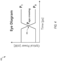
- the DC bias of the EAM is important because it affects when the EAM is blocking/absorbing or transmitting photons (modulating or passing the carrier wave). Determining the correct DC bias is difficult because the correct DC bias changes as the EAM temperature changes. The DC bias affects the eye diagram crossing point, which is used to analyze a given signal's duty cycle issues and transmission quality.
- the goal is to find the correct DC bias to yield a target crossing point (e.g., 50%, 44%), where, as an example, 50% crossing point occurs about halfway horizontally in the middle of a given eye diagram and generally indicates a good duty cycle or quality signal modulation.
- a target crossing point e.g. 50%, 44%)
- Approaches for finding the voltage bias at the target crossing point include using a maximum optical amplitude modulation (OMA) bias (e.g., find the large-signal AC current output from the modulator), or find the maximum dO/dE bias (e.g., find the highest slope or maximum small-signal AC current output from the modulator).
- OMA optical amplitude modulation
- these approaches yield crossing point errors of up to 10% (e.g., 10% off the 50% crossing point), and the crossing point error changes as the RF data rate swing increases. Additionally, these approaches are increasingly inaccurate if the target crossing point is away from 50% (e.g., a 44% target crossing point for PAM4 to increase OMA with minor distortion to the eye, a 62% target crossing point).
- crossing points will change for different modulator designs and, across different process/manufacturing variations, and temperature variations.
- One approach for measuring crossing point can be performed using a high-speed external oscilloscope; however, it is difficult to integrate or is not practical to integrate oscilloscope approaches in modern high-speed optical devices.
- the IF measurement can be implemented by integrating an IF signal generator into the modulator driver (e.g., a high-speed DAC), and the EAM response is measured using an integrated ADC connected to a monitor photodiode that is capable of IF signal detection, where the monitor photodiode is located after the EAM on the transmit optical chain.
- the modulator and monitor photodiode for IF operation, measurement of the EAM response versus voltage bias that is thermally representative of high-speed operation can be performed and RF crossing points can be generated.
- Additional hardware around the monitor photodiode and ADC readout circuit including memory and microprocessor provide support for storing test waveforms or data eyes, and running analysis on these to extract eye parameters.
- the IF and high-speed RF based approach enable the optical device for calibration of any crossing point, not just 50%, which enables accurate calibration of different types of modulator designs and modulation formats.
- An example method is as follows: (1) measure the crossing points for different bias values using an intermediate frequency, (2) generate heating offset from IF to RF, (3) calculate RF crossing points from the IF crossing points and the heating offset values, (4) store RF crossing points in a lookup table, (5) repeat RF crossing points to generate values for different temperatures, (6) during operation, read transceiver temperature and set the DC bias of the modulator based on the lookup table value.
- an IF eye scan based method can be performed as follows: (1) measure the IF eye using an eye scan (e.g., via an ADC, memory, and a microprocessor), (2) measure the IF crossing point directly from the IF eye scan data, (3) apply an adjustment from IF to RF (e.g., via heating offset values) crossing points, (4) repeat for different temperatures (5) during operation read transceiver temperature and set the DC bias based on the lookup table value.
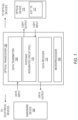
- FIG. 1 is a block diagram illustrating an example optical transceiver 100 for transmitting and receiving optical signals, according to some example embodiments.
- the optical transceiver 100 processes data from electrical devices, such as electrical hardware device 150, converts the electrical data into optical data, and sends and receives the optical data with one or more optical devices, such as optical device 175.
- the electrical hardware device 150 can be a host board that "hosts" the optical transceiver 100 as a pluggable device that sends and receives data to an optical switch network; where, for example, optical device 175 can be other components of an optical switch network (e.g., external transmitter 177).
- the optical transceiver 100 can be implemented to interface with other types of electrical devices and optical devices.
- the optical transceiver 100 can be implemented as a single chip on a hybrid "motherboard" that uses an optical network (e.g., waveguides, fibers) as an optical bus to interconnect on-board electrical chips that process the data after it is converted from light into binary electrical data, according to some example embodiments.
- an optical network e.g., waveguides, fibers
- the hardware device 150 includes an electrical interface for receiving and mating with an electrical interface of the optical transceiver 100.
- the optical transceiver 100 may be a removable front-end module that may be physically received by and removed from hardware device 150 operating as a backend module within a communication system or device.
- the optical transceiver 100 and the hardware device 150 can be components of an optical communication device or system (e.g., a network device) such as a wavelength-division multiplexing (WDM) system or a parallel fiber system (e.g., parallel-single fiber (PSM)), according to some example embodiments.
- WDM wavelength-division multiplexing
- PSM parallel-single fiber
- the optical transceiver 100 includes a microprocessor 102 that controls electrical circuits (e.g., the data transmitter 105, the data receiver 115) and optical components such as the PIC 110.
- electrical circuits e.g., the data transmitter 105, the data receiver 115
- optical components such as the PIC 110.
- the data transmitter 105 of the optical transceiver 100 can receive the electrical signals, which are then converted into optical signals via optical transmitter components (e.g., modulator, heater) of a photonic integrated circuit (PIC) 110.
- the PIC 110 can then output the optical signals via optical links, such as fiber or waveguides that interface with the PIC 110.
- the output light data can then be processed by other components (e.g., switches, endpoint servers, other embedded chips of a single embedded system), via a network such as a wide area network (WAN), optical switch network, optical waveguide network in an embedded system, and others.
- WAN wide area network
- optical switch network optical waveguide network in an embedded system, and others.
- the PIC 110 In receiver mode, the PIC 110 (e.g., photodetector) can receive high data rate optical signals via one or more optical links to optical device 175.
- the optical signals are converted by the optical receiver components in the PIC 110 (e.g., SOA, photodiode), to convert from light into electrical signals for further processing by data receiver 115, such as demodulating the data into a lower data rate for output to other devices, such as the electrical hardware device 150.
- the modulation used by the optical transceiver 100 can include pulse amplitude modulation (e.g., 4-level PAM, such as "PAM4", PAM8, and so on), quadrature phase-shift keying (QPSK), binary phase-shift keying (BPSK), polarization-multiplexed BPSK, M-ary quadrature amplitude modulation (M-QAM), and others.
- pulse amplitude modulation e.g., 4-level PAM, such as "PAM4", PAM8, and so on
- QPSK quadrature phase-shift keying
- BPSK binary phase-shift keying
- M-QAM M-ary quadrature amplitude modulation
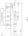
- the receiver circuit 210 is a portion of the data receiver 115 and can include different components (e.g., amplifier, equalizer, high-speed ADC) to process received light that is detected by a high-speed data photodiode 240.
- the readout circuit 215 includes an ADC circuit to receive readout values generated from the monitor photodiode 235, which receives a portion of the light from the modulator 225 via an optical tap 230.
- the tap 230 can direct a fraction of the light towards the monitor photodiode 235 for generation of IF and RF values to identify a target DC bias that yields a target crossing point (e.g., 50%, 40%).
- the readout circuit 215 includes an IF eye scan circuit that generates an IF eye pattern to determine one or more crossing points, as discussed in further detail with reference to FIG. 6 below.
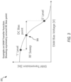
- FIG. 3 shows an example transfer function diagram 300, according to some example embodiments.
- the diagram 300 displays a response of an EAM provided different bias voltages.
- the modulator can be configured with a DC bias that yields a satisfactory eye crossing point, as shown in FIG. 4 .
- the heating from a DC sweep does not simulate the heat of operational high-speed data (e.g., 50 GHz), and existing methods for calibration using high-speed RF exhibit bias voltages that are up to or over 10% away from the target crossing point.
- the IF crossing point is generated using the equation below, where the inputs are the AC electrical current after the modulator ( I AC , IF Mod ), the DC electrical current during IF modulation ( I DC , IF Mod ), and the DC electrical current without modulation ( I DC , No Mod ), where R is response and P is power.
- the RF crossing points are then generated.
- the DC photocurrent at the data frequency (high-speed RF) and at the intermediate frequency (IF) is measured.
- the bias voltage increase required to shift the IF DC photocurrent to the RF DC photocurrent is due to the RF heating, and this is used to calculate the RF crossing point:
- V offset IF to RF I DC , RF Mod ⁇ I DC , IF Mod dV DC , IF Mod dI DC , IF Mod
- I DC,RF Mod and I DC,IF Mod are measured at the same DC bias voltage with RF and IF modulation applied.
- the dV DC,IF Mod / dI DC,IF Mod is the rate of change in I DC,IF Mod for a change in DC bias voltage.
- FIG. 5 shows a flow diagram of a method 500 for intermediate frequency-based calibration of an optical modulator, according to some example embodiments.
- PAM4 and EAMs are discussed as an example, it is appreciated that the intermediate frequency approach can be implemented to other modulation formats and other types of light absorption modulators where high-speed data rates cause crossing point calibration inaccuracies due to heat.
- DC current values with no modulation is measured.
- a laser is set at fixed mission mode power, and the DC voltage bias on the modulator is set to its lowest value (e.g., reverse biased at -1V).
- the modulator is muted, and no intermediate frequency or radio frequency signal is applied to the modulator.
- the DC electrical current from the monitor photodiode that is placed after the modulator is measured to generate a DC electrical current value (e.g., for NRZ, or outer eyes).
- the operation 505 can then be repeated for different DC voltage biases to cover the operating range of the modulator.
- the DC voltage bias on the modulator can be increased to a different value, and the DC electrical current from the monitor photodiode is then remeasured to generate the DC electrical current value at the increased voltage bias.
- Additional voltage biases can be measured in a similar manner at operation 505 until the full operating range is covered (e.g., from -1V to -5V).
- DC and AC current values for intermediate frequency modulation are measured (e.g., for NRZ, or outer eye crossing point).
- the DC voltage bias on the modulator is set to its lowest value (e.g., -1V) and an intermediate square wave signal (e.g., 50 MHz) is applied to the modulator driver to modulate the optical modulator.
- an intermediate square wave signal e.g., 50 MHz
- DC electrical current and AC electrical current are measured using the monitor photodiode placed after the modulator.
- the operation 510 can be repeated for different DC and AC values for different operating ranges.
- the DC voltage bias on the modulator is increased to a new value, the intermediate frequency is reapplied to the modulator, and the DC electrical current and the AC electrical current is remeasured from the monitor photodiode at the new DC voltage bias level. Additional levels of voltage bias may be applied and then AC and DC values measured until the entire operating range is covered.
- DC electrical current is measured while using radio frequency modulation (e.g., measured for NRZ, outer eye crossing).
- the DC voltage bias of the optical modulator is set to its lowest value and the modulator driver is configured to apply a high-speed radiofrequency square wave signal (50 GHz) to the modulator.
- the operational data frequency rate (RF) applied to the modulator the DC electrical current on the monitor photodiode placed after the modulator is then measured.
- the operation 515 is looped to generate additional values for the full operating range. For example, the DC voltage bias is increased, the high-speed radio frequency wave is applied, and the DC current from the monitor photodiode is remeasured at the new bias value.
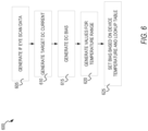
- FIG. 6 shows a flow diagram of an example method 600 for calibration of an optical modulator using intermediate frequency eye scan data, according to some example embodiments.
- an intermediate frequency eye scan in readout circuit 215 is used to generate an eye pattern from which IF and RF crossing points can be generated, according to some example embodiments.
- intermediate frequency eye scan data is generated. For example, IF crossing point calibration operations with IF eye scans are performed using the PAM-4 outer eye only (0-level and 3-level) using an IF eye scan in readout circuit 215.
- the modulator is set to the target crossing value for IF modulation (e.g., V DC Bias at Crossing Target ) and the modulator driver in the signal circuit 205 is turned on with an IF PAM-4 test pattern.
- the eyes of the IF PAM4 wave are then measured using the IF eye scan module (e.g., high-speed ADC with memory to store the test pattern output, and microprocessor to analyze data) and the PAM eye quality metric data is calculated (e.g., ratio-level-mismatch (RLM), inner eye OMAs) and only the eye quality calculations are then stored.
- the combinations of 1-level and 2-level voltage offsets are then stepped through while keeping the outer swing fixed, and then remeasuring after each step. At each step, the calculated eye quality is stored in a table for reference.
- additional modulator values for a full operating temperature range are generated. After performing the previous operations at a first temperature, the first transceiver temperature, DC bias, 1-level, and 2-level values are then saved to integrated memory as a lookup table. Next, at a second temperature, the above operations are repeated to generate DC bias, 1-level, and 2-level values which are stored with the second temperature in the lookup table. Further, additional values for different temperatures can then be generated by interpolating the data between the first and second temperatures, and further by using the data from the two temperatures points to extrapolate to additional temperatures above and below the first and second temperatures. Once the values are generated for the full range of temperatures, the data is then stored to memory in the lookup table for reference during operation.
- FIG. 7 is an illustration of an optical-electrical device 700 including one or more optical devices, according to an embodiment of the disclosure.
- the optical-electrical device 700 is a multi-structure chip package that includes a printed circuit board (PCB) substrate 705, organic substrate 710, application specific integrated circuit (ASIC) 715, and photonic integrated circuit (PIC) 720.
- the PIC 720 may include one or more optical structures described above (e.g., PIC 110).
- the PIC 720 includes silicon on insulator (SOI) or silicon-based (e.g., silicon nitride (SiN)) devices, or may comprise devices formed from both silicon and a non-silicon material.
- Said non-silicon material (alternatively referred to as "heterogeneous material") may comprise one of III-V material, magneto-optic material, or crystal substrate material.
- III-V semiconductors have elements that are found in group III and group V of the periodic table (e.g., Indium Gallium Arsenide Phosphide (InGaAsP), Gallium Indium Arsenide Nitride (GainAsN)).
- III-V-based materials may be significantly higher than in silicon-based materials, as electron speed in III-V semiconductors is much faster than that in silicon.
- III-V materials have a direct bandgap which enables efficient creation of light from electrical pumping.
- III-V semiconductor materials enable photonic operations with an increased efficiency over silicon for both generating light and modulating the refractive index of light.
- III-V semiconductor materials enable photonic operation with an increased efficiency at generating light from electricity and converting light back into electricity.
- the low optical loss and high quality oxides of silicon are thus combined with the electro-optic efficiency of III-V semiconductors in the heterogeneous optical devices described below; in embodiments of the disclosure, said heterogeneous devices utilize low loss heterogeneous optical waveguide transitions between the devices' heterogeneous and silicon-only waveguides.
- Magneto-optic materials allow heterogeneous PICs to operate based on the magneto-optic (MO) effect. Such devices may utilize the Faraday Effect, in which the magnetic field associated with an electrical signal modulates an optical beam, offering high bandwidth modulation, and rotates the electric field of the optical mode enabling optical isolators.
- Said magneto-optic materials may comprise, for example, materials such as iron, cobalt, or yttrium iron garnet (YIG).
- crystal substrate materials provide heterogeneous PICs with a high electro-mechanical coupling, linear electro optic coefficient, low transmission loss, and stable physical and chemical properties.
- Said crystal substrate materials may comprise, for example, lithium niobate (LiNbO3) or lithium tantalate (LiTaO3).
- the PIC 720 exchanges light with fiber 730 via prism 725; said prism 725 is a misalignment-tolerant device used to couple an optical mode to one or more single-mode optical fibers (e.g., to transmit light to and from an optical network), according to some example embodiments.
- the optical devices of PIC 720 are controlled, at least in part, by control circuitry included in ASIC 715. Both ASIC 715 and PIC 720 are shown to be disposed on copper pillars 714, which are used for communicatively coupling the ICs via organic substrate 710.
- PCB 705 is coupled to organic substrate 710 via ball grid array (BGA) interconnect 716, and may be used to interconnect the organic substrate 710 (and thus, ASIC 715 and PIC 720) to other components of optical-electrical device 700 not shown, such as interconnection modules, power supplies, and so forth.
- BGA ball grid array
- an optical modulator of an optical transceiver that can be calibrated using intermediate frequency (IF) signals to generate accurate crossing point values (e.g., DC bias).
- IF intermediate frequency
- a photodiode can measure output from the optical modulator at intermediate and high-speed frequencies to generate crossing point values that avoid crossing point errors.
- a target crossing point can be selected at any value (e.g., 40%, 50%) and bias values can be generated from IF signals and then stored in a lookup date for setting the modulator bias during operation.
Landscapes
- Physics & Mathematics (AREA)
- Electromagnetism (AREA)
- Engineering & Computer Science (AREA)
- Computer Networks & Wireless Communication (AREA)
- Signal Processing (AREA)
- Nonlinear Science (AREA)
- General Physics & Mathematics (AREA)
- Optics & Photonics (AREA)
- Optical Modulation, Optical Deflection, Nonlinear Optics, Optical Demodulation, Optical Logic Elements (AREA)
- Optical Communication System (AREA)
Claims (15)
- Verfahren zum Verarbeiten von Licht unter Verwendung eines optischen Transceivers (100), das Verfahren umfassend:Empfangen, durch einen Elektroabsorptionsmodulator, EAM, des optischen Transceivers (100), von Licht, das von einer Lichtquelle (220) erzeugt wird;Erzeugen von moduliertem Licht durch Modulieren des Lichts bei einer Funkfrequenz- bzw. HF-Datenrate hoher Geschwindigkeit unter Verwendung des EAM, wobei der EAM einen Kreuzungspunkt (405) aufweist, der gemäß einer Zwischenfrequenz- bzw. ZF-Datenrate, die niedriger als die HF-Datenrate hoher Geschwindigkeit ist, eingestellt ist; undÜbertragen des modulierten Lichts unter Verwendung des optischen Transceivers (100).
- Verfahren nach Anspruch 1, wobei die ZF-Datenrate eine Frequenz ist, die mindestens eine Größenordnung kleiner als die HF-Datenrate ist.
- Verfahren nach Anspruch 1 oder Anspruch 2, wobei die HF-Datenrate eine Frequenz hoher Geschwindigkeit ist, die Erwärmungsungenauigkeiten bei der Messung des Kreuzungspunkts des EAM verursacht, wobei die ZF-Datenrate aus einem Frequenzbereich ist, der niedrig genug ist, um Erwärmungsungenauigkeiten bei der Messung des Kreuzungspunkts des EAM zu vermeiden, und hoch genug ist, um über einer thermischen Ansprechzeit des EAM zu sein, um Erwärmungsübergangseffekte während der Modulation zu vermeiden.
- Verfahren nach einem der vorhergehenden Ansprüche, wobei der optische Transceiver (100) einen Signalgenerator umfasst, der konfiguriert ist, ein ZF-Signal und ein HF-Signal hoher Geschwindigkeit dem EAM bereitzustellen.
- Verfahren nach einem der vorhergehenden Ansprüche, wobei der Kreuzungspunkt von einem Vorspannungswert, der in einer Nachschlagetabelle in dem optischen Transceiver (100) gespeichert ist, eingestellt wird und wobei wahlweise der Vorspannungswert durch Anwenden der ZF-Datenrate bei einer Amplitude ähnlich der ZF-Datenrate auf den EAM erzeugt wird, um den Kreuzungspunkt zu bestimmen.
- Verfahren nach einem der vorhergehenden Ansprüche, wobei die Lichtquelle eine eingebettete Lichtquelle ist, die in den optischen Transceiver (100) integriert ist.
- Verfahren nach Anspruch 6, wobei die eingebettete Lichtquelle eine III-V-Schicht zum Erzeugen von Licht umfasst.
- Verfahren nach einem der vorhergehenden Ansprüche, wobei der optische Transceiver (100) eine Überwachungsfotodiode (235) zum Messen der Ausgabe von dem EAM und eine ZF-Augenabtastschaltung zum Erzeugen von Augenabtastungsdaten aus Ausgabe der Überwachungsfotodiode (235) umfasst.
- Optischer Transceiver (100), umfassend:einen Eingabe-Lichtweg zum Empfangen von Licht, das von einer Lichtquelle (220) erzeugt wird;einen Elektroabsorptionsmodulator, EAM, zum Erzeugen von moduliertem Licht durch Modulieren des Lichts bei einer Funkfrequenz- bzw. HF-Datenrate hoher Geschwindigkeit, wobei der EAM einen Kreuzungspunkt (405) aufweist, der gemäß einer Zwischenfrequenz- bzw. ZF-Datenrate, die niedriger als die HF-Datenrate hoher Geschwindigkeit ist, eingestellt ist; undeinen Ausgabe-Lichtweg zum Übertragen des modulierten Lichts.
- Optischer Transceiver (100) nach Anspruch 9, wobei die ZF-Datenrate eine Frequenz ist, die mindestens eine Größenordnung kleiner als die HF-Datenrate ist.
- Optischer Transceiver (100) nach Anspruch 10, wobei die HF-Datenrate eine Frequenz hoher Geschwindigkeit ist, die Erwärmungsungenauigkeiten bei der Messung des Kreuzungspunkts des EAM verursacht, wobei die ZF-Datenrate aus einem Frequenzbereich ist, der niedrig genug ist, um Erwärmungsungenauigkeiten bei der Messung des Kreuzungspunkts des EAM zu vermeiden, und hoch genug ist, um über der thermischen Ansprechzeit des EAM zu sein, um Erwärmungsübergangseffekte während der Modulation zu vermeiden.
- Optischer Transceiver (100) nach einem der Ansprüche 9 bis 11, wobei der optische Transceiver (100) einen Signalgenerator umfasst, der konfiguriert ist, ein ZF-Signal und ein HF-Signal hoher Geschwindigkeit dem EAM bereitzustellen.
- Optischer Transceiver (100) nach einem der Ansprüche 9 bis 12, wobei der Kreuzungspunkt von einem Vorspannungswert, der in einer Nachschlagetabelle in dem optischen Transceiver (100) gespeichert ist, eingestellt wird und wobei wahlweise der Vorspannungswert durch Anwenden der ZF-Datenrate bei einer Amplitude ähnlich der ZF-Datenrate auf den EAM erzeugt wird, um den Kreuzungspunkt zu bestimmen.
- Optischer Transceiver (100) nach einem der Ansprüche 9 bis 13, wobei die Lichtquelle eine eingebettete Lichtquelle ist, die in den optischen Transceiver (100) integriert ist.
- Optischer Transceiver (100) nach einem der Ansprüche 9 bis 14, wobei der optische Transceiver (100) eine Überwachungsfotodiode (235) zum Messen der Ausgabe von dem EAM und eine ZF-Augenabtastschaltung zum Erzeugen von Augenabtastungsdaten aus Ausgabe der Überwachungsfotodiode (235) umfasst.
Applications Claiming Priority (1)
| Application Number | Priority Date | Filing Date | Title |
|---|---|---|---|
| US17/001,951 US10998979B1 (en) | 2020-08-25 | 2020-08-25 | Intermediate frequency calibrated optical modulators |
Publications (3)
| Publication Number | Publication Date |
|---|---|
| EP3961940A1 EP3961940A1 (de) | 2022-03-02 |
| EP3961940C0 EP3961940C0 (de) | 2025-06-25 |
| EP3961940B1 true EP3961940B1 (de) | 2025-06-25 |
Family
ID=73455517
Family Applications (1)
| Application Number | Title | Priority Date | Filing Date |
|---|---|---|---|
| EP20207792.1A Active EP3961940B1 (de) | 2020-08-25 | 2020-11-16 | Kalibrierte optische zwischenfrequenzmodulatoren und methode |
Country Status (3)
| Country | Link |
|---|---|
| US (2) | US10998979B1 (de) |
| EP (1) | EP3961940B1 (de) |
| CN (1) | CN114124236B (de) |
Families Citing this family (4)
| Publication number | Priority date | Publication date | Assignee | Title |
|---|---|---|---|---|
| US10998979B1 (en) | 2020-08-25 | 2021-05-04 | Juniper Networks, Inc. | Intermediate frequency calibrated optical modulators |
| JP7633640B2 (ja) * | 2020-08-26 | 2025-02-20 | 7Gaa株式会社 | 光伝送モジュール、光データリンクおよび光伝送システム |
| US11616578B2 (en) * | 2021-08-13 | 2023-03-28 | Macom Technology Solutions Holdings, Inc. | Adjusting eye heights and optical power levels of a multi-level optical signal |
| CN116131940B (zh) * | 2023-04-17 | 2023-07-07 | 广州赛宝计量检测中心服务有限公司 | 光不连续性测试仪校准装置、系统及方法 |
Family Cites Families (16)
| Publication number | Priority date | Publication date | Assignee | Title |
|---|---|---|---|---|
| US20020012495A1 (en) * | 2000-06-29 | 2002-01-31 | Hiroyuki Sasai | Optical transmission system for radio access and high frequency optical transmitter |
| US7116851B2 (en) * | 2001-10-09 | 2006-10-03 | Infinera Corporation | Optical signal receiver, an associated photonic integrated circuit (RxPIC), and method improving performance |
| US7751658B2 (en) * | 2001-10-09 | 2010-07-06 | Infinera Corporation | Monolithic transmitter photonic integrated circuit (TxPIC) having tunable modulated sources with feedback system for source power level or wavelength tuning |
| CN1270442C (zh) * | 2004-08-20 | 2006-08-16 | 清华大学 | 基于电吸收调制器的光电混合锁相环路 |
| CA2612165C (en) * | 2005-06-30 | 2015-05-19 | Infinera Corporation | Wavelength locking and power control systems for multi-channel photonic integrated circuits (pics) |
| US20080101795A1 (en) * | 2006-10-27 | 2008-05-01 | Craig Schulz | Data signal amplitude and cross-point detectors in an optical modulator control system |
| CN101459913B (zh) * | 2007-12-12 | 2010-10-27 | 华为技术有限公司 | 无线通信系统、中心站、接入设备及通信方法 |
| US7917041B2 (en) * | 2008-02-20 | 2011-03-29 | Finisar Corporation | Variable optical attenuator integration into transmitter optical subassemblies |
| US9716553B2 (en) * | 2012-04-30 | 2017-07-25 | Telefonaktiebolaget Lm Ericsson (Publ) | Radio frequency signal transceiver, coherent radar receiver and method of processing radio frequency signals |
| JP2014106492A (ja) * | 2012-11-29 | 2014-06-09 | Fujitsu Ltd | 光信号処理装置及び光信号処理方法 |
| US9252886B2 (en) * | 2013-01-24 | 2016-02-02 | Sumitomo Electric Industries, Ltd. | Optical transmitter |
| US9722722B2 (en) * | 2014-09-19 | 2017-08-01 | Neophotonics Corporation | Dense wavelength division multiplexing and single-wavelength transmission systems |
| US9698911B2 (en) * | 2015-06-30 | 2017-07-04 | Lockheed Martin Corporation | Systems, devices, and methods for photonic to radio frequency downconversion |
| US9658477B2 (en) * | 2015-06-30 | 2017-05-23 | Lockheed Martin Corporation | Systems, devices, and methods for photonic to radio frequency upconversion |
| US10401495B2 (en) * | 2017-07-10 | 2019-09-03 | Blackmore Sensors and Analytics Inc. | Method and system for time separated quadrature detection of doppler effects in optical range measurements |
| US10998979B1 (en) | 2020-08-25 | 2021-05-04 | Juniper Networks, Inc. | Intermediate frequency calibrated optical modulators |
-
2020
- 2020-08-25 US US17/001,951 patent/US10998979B1/en active Active
- 2020-11-16 CN CN202011278708.5A patent/CN114124236B/zh active Active
- 2020-11-16 EP EP20207792.1A patent/EP3961940B1/de active Active
-
2021
- 2021-04-05 US US17/222,200 patent/US11671178B2/en active Active
Also Published As
| Publication number | Publication date |
|---|---|
| EP3961940A1 (de) | 2022-03-02 |
| US11671178B2 (en) | 2023-06-06 |
| CN114124236B (zh) | 2023-06-13 |
| US10998979B1 (en) | 2021-05-04 |
| CN114124236A (zh) | 2022-03-01 |
| US20220069917A1 (en) | 2022-03-03 |
| EP3961940C0 (de) | 2025-06-25 |
Similar Documents
| Publication | Publication Date | Title |
|---|---|---|
| EP3961940B1 (de) | Kalibrierte optische zwischenfrequenzmodulatoren und methode | |
| Sepehrian et al. | Silicon photonic IQ modulators for 400 Gb/s and beyond | |
| Patel et al. | Silicon photonic segmented modulator-based electro-optic DAC for 100 Gb/s PAM-4 generation | |
| US9323128B1 (en) | Off quadrature biasing of mach zehnder modulator for improved OSNR performance | |
| Schindler et al. | Monolithic GaAs electro-optic IQ modulator demonstrated at 150 Gbit/s with 64QAM | |
| KR102663758B1 (ko) | 내장형 자체 테스트를 갖는 하이-레인 카운트 광학 트랜시버 | |
| Seiler et al. | Multiband silicon photonic ePIC coherent receiver for 64 GBd QPSK | |
| Jiang et al. | Electro-optic crosstalk in parallel silicon photonic Mach-Zehnder modulators | |
| Dev et al. | Compact and energy-efficient forward-biased PN silicon Mach-Zehnder modulator | |
| US20220038176A1 (en) | Multi-lane optical-electrical device testing using automated testing equipment | |
| Hai et al. | A ring-based 25 Gb/s DAC-less PAM-4 modulator | |
| Groumas et al. | Multi-100 GbE and 400 GbE interfaces for intra-data center networks based on arrayed transceivers with serial 100 Gb/s operation | |
| Zwickel et al. | Electrically packaged silicon-organic hybrid (SOH) I/Q-modulator for 64 GBd operation | |
| CN107835053A (zh) | 一种高精度瞬时微波频率测量装置 | |
| Zhu et al. | Optimized silicon QPSK modulator with 64-Gb/s modulation speed | |
| JP3937237B2 (ja) | 光周波数シフトキーイング変調器 | |
| US7526209B2 (en) | Optical frequency shift keying modulator | |
| Wang et al. | Photonic generation of multi-format radar waveforms based on an integrated silicon IQ modulator | |
| El-Fiky et al. | A 4-lane 400 Gb/s silicon photonic transceiver for intra-datacenter optical interconnects | |
| Wang et al. | Frequency-and time-domain modeling and characterization of PN phase shifters in all-silicon carrier-depletion modulators | |
| Cammarata et al. | 30 Gb/s NRZ transmission with lumped-element silicon photonic mach-Zehnder modulator | |
| Cano et al. | 25-Gb/s laser modulated EML with high output power | |
| Dev et al. | Energy-Efficient Forward-Biased PIN Silicon Mach–Zehnder Modulator With 50 μm Active Phase Shifter Length | |
| Hössbacher et al. | Broadband plasmonic modulator enabling single carrier operation beyond 100 Gbit/s | |
| JP2011238863A (ja) | 光変調度制御回路 |
Legal Events
| Date | Code | Title | Description |
|---|---|---|---|
| PUAI | Public reference made under article 153(3) epc to a published international application that has entered the european phase |
Free format text: ORIGINAL CODE: 0009012 |
|
| STAA | Information on the status of an ep patent application or granted ep patent |
Free format text: STATUS: THE APPLICATION HAS BEEN PUBLISHED |
|
| AK | Designated contracting states |
Kind code of ref document: A1 Designated state(s): AL AT BE BG CH CY CZ DE DK EE ES FI FR GB GR HR HU IE IS IT LI LT LU LV MC MK MT NL NO PL PT RO RS SE SI SK SM TR |
|
| STAA | Information on the status of an ep patent application or granted ep patent |
Free format text: STATUS: REQUEST FOR EXAMINATION WAS MADE |
|
| 17P | Request for examination filed |
Effective date: 20220901 |
|
| RBV | Designated contracting states (corrected) |
Designated state(s): AL AT BE BG CH CY CZ DE DK EE ES FI FR GB GR HR HU IE IS IT LI LT LU LV MC MK MT NL NO PL PT RO RS SE SI SK SM TR |
|
| RAP1 | Party data changed (applicant data changed or rights of an application transferred) |
Owner name: OPENLIGHT PHOTONICS, INC. |
|
| GRAP | Despatch of communication of intention to grant a patent |
Free format text: ORIGINAL CODE: EPIDOSNIGR1 |
|
| STAA | Information on the status of an ep patent application or granted ep patent |
Free format text: STATUS: GRANT OF PATENT IS INTENDED |
|
| INTG | Intention to grant announced |
Effective date: 20240717 |
|
| GRAJ | Information related to disapproval of communication of intention to grant by the applicant or resumption of examination proceedings by the epo deleted |
Free format text: ORIGINAL CODE: EPIDOSDIGR1 |
|
| STAA | Information on the status of an ep patent application or granted ep patent |
Free format text: STATUS: REQUEST FOR EXAMINATION WAS MADE |
|
| INTC | Intention to grant announced (deleted) | ||
| GRAP | Despatch of communication of intention to grant a patent |
Free format text: ORIGINAL CODE: EPIDOSNIGR1 |
|
| STAA | Information on the status of an ep patent application or granted ep patent |
Free format text: STATUS: GRANT OF PATENT IS INTENDED |
|
| INTG | Intention to grant announced |
Effective date: 20250116 |
|
| GRAS | Grant fee paid |
Free format text: ORIGINAL CODE: EPIDOSNIGR3 |
|
| GRAA | (expected) grant |
Free format text: ORIGINAL CODE: 0009210 |
|
| STAA | Information on the status of an ep patent application or granted ep patent |
Free format text: STATUS: THE PATENT HAS BEEN GRANTED |
|
| AK | Designated contracting states |
Kind code of ref document: B1 Designated state(s): AL AT BE BG CH CY CZ DE DK EE ES FI FR GB GR HR HU IE IS IT LI LT LU LV MC MK MT NL NO PL PT RO RS SE SI SK SM TR |
|
| REG | Reference to a national code |
Ref country code: GB Ref legal event code: FG4D |
|
| REG | Reference to a national code |
Ref country code: CH Ref legal event code: EP |
|
| REG | Reference to a national code |
Ref country code: CH Ref legal event code: EP |
|
| REG | Reference to a national code |
Ref country code: IE Ref legal event code: FG4D |
|
| REG | Reference to a national code |
Ref country code: DE Ref legal event code: R096 Ref document number: 602020053224 Country of ref document: DE |
|
| U01 | Request for unitary effect filed |
Effective date: 20250718 |
|
| U07 | Unitary effect registered |
Designated state(s): AT BE BG DE DK EE FI FR IT LT LU LV MT NL PT RO SE SI Effective date: 20250725 |
|
| PG25 | Lapsed in a contracting state [announced via postgrant information from national office to epo] |
Ref country code: NO Free format text: LAPSE BECAUSE OF FAILURE TO SUBMIT A TRANSLATION OF THE DESCRIPTION OR TO PAY THE FEE WITHIN THE PRESCRIBED TIME-LIMIT Effective date: 20250925 Ref country code: GR Free format text: LAPSE BECAUSE OF FAILURE TO SUBMIT A TRANSLATION OF THE DESCRIPTION OR TO PAY THE FEE WITHIN THE PRESCRIBED TIME-LIMIT Effective date: 20250926 |
|
| PG25 | Lapsed in a contracting state [announced via postgrant information from national office to epo] |
Ref country code: HR Free format text: LAPSE BECAUSE OF FAILURE TO SUBMIT A TRANSLATION OF THE DESCRIPTION OR TO PAY THE FEE WITHIN THE PRESCRIBED TIME-LIMIT Effective date: 20250625 |
|
| PG25 | Lapsed in a contracting state [announced via postgrant information from national office to epo] |
Ref country code: RS Free format text: LAPSE BECAUSE OF FAILURE TO SUBMIT A TRANSLATION OF THE DESCRIPTION OR TO PAY THE FEE WITHIN THE PRESCRIBED TIME-LIMIT Effective date: 20250925 |
|
| U20 | Renewal fee for the european patent with unitary effect paid |
Year of fee payment: 6 Effective date: 20251113 |