EP3961922A1 - Method for manufacturing sensor device and sensor device - Google Patents
Method for manufacturing sensor device and sensor device Download PDFInfo
- Publication number
- EP3961922A1 EP3961922A1 EP20795475.1A EP20795475A EP3961922A1 EP 3961922 A1 EP3961922 A1 EP 3961922A1 EP 20795475 A EP20795475 A EP 20795475A EP 3961922 A1 EP3961922 A1 EP 3961922A1
- Authority
- EP
- European Patent Office
- Prior art keywords
- immobilized layer
- idt electrode
- sensor device
- layer
- immobilized
- Prior art date
- Legal status (The legal status is an assumption and is not a legal conclusion. Google has not performed a legal analysis and makes no representation as to the accuracy of the status listed.)
- Withdrawn
Links
- 238000004519 manufacturing process Methods 0.000 title claims description 11
- 238000000034 method Methods 0.000 title description 8
- 239000000758 substrate Substances 0.000 claims abstract description 65
- 230000001681 protective effect Effects 0.000 claims abstract description 45
- 239000000463 material Substances 0.000 claims description 24
- 230000003746 surface roughness Effects 0.000 claims description 12
- 229910052751 metal Inorganic materials 0.000 claims description 10
- 239000002184 metal Substances 0.000 claims description 10
- 238000010897 surface acoustic wave method Methods 0.000 description 57
- 239000010931 gold Substances 0.000 description 21
- 239000000427 antigen Substances 0.000 description 17
- 108091007433 antigens Proteins 0.000 description 17
- 102000036639 antigens Human genes 0.000 description 17
- 238000001514 detection method Methods 0.000 description 14
- 238000005530 etching Methods 0.000 description 12
- 229910052737 gold Inorganic materials 0.000 description 11
- PCHJSUWPFVWCPO-UHFFFAOYSA-N gold Chemical compound [Au] PCHJSUWPFVWCPO-UHFFFAOYSA-N 0.000 description 10
- 230000035945 sensitivity Effects 0.000 description 8
- 230000000694 effects Effects 0.000 description 7
- 108091023037 Aptamer Proteins 0.000 description 6
- 239000010936 titanium Substances 0.000 description 6
- BOTDANWDWHJENH-UHFFFAOYSA-N Tetraethyl orthosilicate Chemical compound CCO[Si](OCC)(OCC)OCC BOTDANWDWHJENH-UHFFFAOYSA-N 0.000 description 5
- 238000006243 chemical reaction Methods 0.000 description 5
- 230000000644 propagated effect Effects 0.000 description 5
- 239000000126 substance Substances 0.000 description 5
- 108090000790 Enzymes Proteins 0.000 description 4
- 102000004190 Enzymes Human genes 0.000 description 4
- 238000011088 calibration curve Methods 0.000 description 4
- 238000001312 dry etching Methods 0.000 description 4
- RTAQQCXQSZGOHL-UHFFFAOYSA-N Titanium Chemical compound [Ti] RTAQQCXQSZGOHL-UHFFFAOYSA-N 0.000 description 3
- 229910052782 aluminium Inorganic materials 0.000 description 3
- XAGFODPZIPBFFR-UHFFFAOYSA-N aluminium Chemical compound [Al] XAGFODPZIPBFFR-UHFFFAOYSA-N 0.000 description 3
- 238000005260 corrosion Methods 0.000 description 3
- 230000007797 corrosion Effects 0.000 description 3
- 230000003647 oxidation Effects 0.000 description 3
- 238000007254 oxidation reaction Methods 0.000 description 3
- 238000001020 plasma etching Methods 0.000 description 3
- 229920006254 polymer film Polymers 0.000 description 3
- 239000013076 target substance Substances 0.000 description 3
- 229910052719 titanium Inorganic materials 0.000 description 3
- 238000001039 wet etching Methods 0.000 description 3
- VYZAMTAEIAYCRO-UHFFFAOYSA-N Chromium Chemical compound [Cr] VYZAMTAEIAYCRO-UHFFFAOYSA-N 0.000 description 2
- 244000126211 Hericium coralloides Species 0.000 description 2
- OAICVXFJPJFONN-UHFFFAOYSA-N Phosphorus Chemical compound [P] OAICVXFJPJFONN-UHFFFAOYSA-N 0.000 description 2
- 238000004458 analytical method Methods 0.000 description 2
- 238000013459 approach Methods 0.000 description 2
- 238000005229 chemical vapour deposition Methods 0.000 description 2
- 230000001276 controlling effect Effects 0.000 description 2
- 239000010949 copper Substances 0.000 description 2
- 238000012937 correction Methods 0.000 description 2
- 238000012986 modification Methods 0.000 description 2
- 230000004048 modification Effects 0.000 description 2
- 238000000059 patterning Methods 0.000 description 2
- 239000011347 resin Substances 0.000 description 2
- 229920005989 resin Polymers 0.000 description 2
- VYPSYNLAJGMNEJ-UHFFFAOYSA-N silicon dioxide Inorganic materials O=[Si]=O VYPSYNLAJGMNEJ-UHFFFAOYSA-N 0.000 description 2
- 238000004544 sputter deposition Methods 0.000 description 2
- 229910016570 AlCu Inorganic materials 0.000 description 1
- RYGMFSIKBFXOCR-UHFFFAOYSA-N Copper Chemical compound [Cu] RYGMFSIKBFXOCR-UHFFFAOYSA-N 0.000 description 1
- NINIDFKCEFEMDL-UHFFFAOYSA-N Sulfur Chemical compound [S] NINIDFKCEFEMDL-UHFFFAOYSA-N 0.000 description 1
- 239000002253 acid Substances 0.000 description 1
- 239000012670 alkaline solution Substances 0.000 description 1
- 239000000956 alloy Substances 0.000 description 1
- 229910045601 alloy Inorganic materials 0.000 description 1
- 150000001412 amines Chemical class 0.000 description 1
- 230000005540 biological transmission Effects 0.000 description 1
- 239000008280 blood Substances 0.000 description 1
- 210000004369 blood Anatomy 0.000 description 1
- 239000000919 ceramic Substances 0.000 description 1
- 239000003153 chemical reaction reagent Substances 0.000 description 1
- 239000003795 chemical substances by application Substances 0.000 description 1
- 238000009833 condensation Methods 0.000 description 1
- 230000005494 condensation Effects 0.000 description 1
- 229910052802 copper Inorganic materials 0.000 description 1
- 230000008878 coupling Effects 0.000 description 1
- 238000010168 coupling process Methods 0.000 description 1
- 238000005859 coupling reaction Methods 0.000 description 1
- 230000007423 decrease Effects 0.000 description 1
- 238000005516 engineering process Methods 0.000 description 1
- 238000007667 floating Methods 0.000 description 1
- 239000011810 insulating material Substances 0.000 description 1
- 238000005259 measurement Methods 0.000 description 1
- 239000000203 mixture Substances 0.000 description 1
- 108020004707 nucleic acids Proteins 0.000 description 1
- 102000039446 nucleic acids Human genes 0.000 description 1
- 150000007523 nucleic acids Chemical class 0.000 description 1
- 238000000206 photolithography Methods 0.000 description 1
- 229920000642 polymer Polymers 0.000 description 1
- 102000004196 processed proteins & peptides Human genes 0.000 description 1
- 108090000765 processed proteins & peptides Proteins 0.000 description 1
- 238000012545 processing Methods 0.000 description 1
- 239000010453 quartz Substances 0.000 description 1
- 230000001105 regulatory effect Effects 0.000 description 1
- 210000003296 saliva Anatomy 0.000 description 1
- 229910052814 silicon oxide Inorganic materials 0.000 description 1
- 239000000243 solution Substances 0.000 description 1
- 238000000992 sputter etching Methods 0.000 description 1
- 229910052717 sulfur Inorganic materials 0.000 description 1
- 239000011593 sulfur Substances 0.000 description 1
- 210000002700 urine Anatomy 0.000 description 1
Images






Classifications
-
- G—PHYSICS
- G01—MEASURING; TESTING
- G01N—INVESTIGATING OR ANALYSING MATERIALS BY DETERMINING THEIR CHEMICAL OR PHYSICAL PROPERTIES
- G01N29/00—Investigating or analysing materials by the use of ultrasonic, sonic or infrasonic waves; Visualisation of the interior of objects by transmitting ultrasonic or sonic waves through the object
- G01N29/22—Details, e.g. general constructional or apparatus details
- G01N29/24—Probes
- G01N29/2462—Probes with waveguides, e.g. SAW devices
-
- G—PHYSICS
- G01—MEASURING; TESTING
- G01N—INVESTIGATING OR ANALYSING MATERIALS BY DETERMINING THEIR CHEMICAL OR PHYSICAL PROPERTIES
- G01N29/00—Investigating or analysing materials by the use of ultrasonic, sonic or infrasonic waves; Visualisation of the interior of objects by transmitting ultrasonic or sonic waves through the object
- G01N29/02—Analysing fluids
- G01N29/022—Fluid sensors based on microsensors, e.g. quartz crystal-microbalance [QCM], surface acoustic wave [SAW] devices, tuning forks, cantilevers, flexural plate wave [FPW] devices
-
- G—PHYSICS
- G01—MEASURING; TESTING
- G01N—INVESTIGATING OR ANALYSING MATERIALS BY DETERMINING THEIR CHEMICAL OR PHYSICAL PROPERTIES
- G01N2291/00—Indexing codes associated with group G01N29/00
- G01N2291/01—Indexing codes associated with the measuring variable
- G01N2291/011—Velocity or travel time
-
- G—PHYSICS
- G01—MEASURING; TESTING
- G01N—INVESTIGATING OR ANALYSING MATERIALS BY DETERMINING THEIR CHEMICAL OR PHYSICAL PROPERTIES
- G01N2291/00—Indexing codes associated with group G01N29/00
- G01N2291/01—Indexing codes associated with the measuring variable
- G01N2291/012—Phase angle
-
- G—PHYSICS
- G01—MEASURING; TESTING
- G01N—INVESTIGATING OR ANALYSING MATERIALS BY DETERMINING THEIR CHEMICAL OR PHYSICAL PROPERTIES
- G01N2291/00—Indexing codes associated with group G01N29/00
- G01N2291/02—Indexing codes associated with the analysed material
- G01N2291/025—Change of phase or condition
- G01N2291/0255—(Bio)chemical reactions, e.g. on biosensors
-
- G—PHYSICS
- G01—MEASURING; TESTING
- G01N—INVESTIGATING OR ANALYSING MATERIALS BY DETERMINING THEIR CHEMICAL OR PHYSICAL PROPERTIES
- G01N2291/00—Indexing codes associated with group G01N29/00
- G01N2291/02—Indexing codes associated with the analysed material
- G01N2291/025—Change of phase or condition
- G01N2291/0256—Adsorption, desorption, surface mass change, e.g. on biosensors
-
- G—PHYSICS
- G01—MEASURING; TESTING
- G01N—INVESTIGATING OR ANALYSING MATERIALS BY DETERMINING THEIR CHEMICAL OR PHYSICAL PROPERTIES
- G01N2291/00—Indexing codes associated with group G01N29/00
- G01N2291/04—Wave modes and trajectories
- G01N2291/042—Wave modes
- G01N2291/0423—Surface waves, e.g. Rayleigh waves, Love waves
Definitions
- the present disclosure relates to a method of manufacturing a sensor device and a sensor device.
- a known surface acoustic wave device has a configuration in which an electrode that generates a surface acoustic wave is covered by a film (see, for example, PTL 1) .
- a sensor device includes a substrate having a substrate surface, a first IDT electrode positioned on the substrate surface, a second IDT electrode positioned on the substrate surface, a waveguide, and a protective film.
- the waveguide is positioned on the substrate surface and between the first IDT electrode and the second IDT electrode.
- the waveguide includes a first immobilized layer positioned on the substrate surface and a second immobilized layer positioned on the first immobilized layer.
- the second immobilized layer is positioned inside an outer edge of the first immobilized layer as seen in a plan view.
- a method of manufacturing a sensor device includes a step of forming a metal layer on a substrate.
- the method includes a step of removing a part of the metal layer to form a first IDT electrode, a second IDT electrode, and a first immobilized layer positioned between the first IDT electrode and the second IDT electrode.
- the method includes a step of forming a protective film that covers the first IDT electrode, the second IDT electrode, and the first immobilized layer.
- the method includes a step of removing a part of the protective film to expose at least a part of the first immobilized layer.
- the method includes a step of forming a second immobilized layer on at least a part of an exposed surface of the first immobilized layer.
- a surface acoustic wave device detects a change in a state on a waveguide by detecting a propagation state of a surface acoustic wave. It is required to improve the accuracy in detection of the change in the state on the waveguide.
- a sensor device 1 (see Fig. 1 ) according to an embodiment of the present disclosure and a method of manufacturing the sensor device 1 can improve the accuracy in detection of a surface state of a waveguide.
- the sensor device 1 includes a substrate 10, a first IDT (interdigital transducer) electrode 11, a second IDT electrode 12, and a waveguide 20.
- the sensor device 1 functions as a SAW sensor that can detect a change in the propagation characteristics of a surface acoustic wave (SAW) 70.
- the sensor device 1 inputs an alternate-current electric signal to the first IDT electrode 11.
- the first IDT electrode 11 generates the SAW 70 along a surface of the substrate 10 based on the input electric signal.
- the SAW 70 propagates from the first IDT electrode 11 to the second IDT electrode 12.
- the propagation path from the first IDT electrode 11 to the second IDT electrode 12 includes a surface of the substrate 10 and the waveguide 20 positioned on the surface of the substrate 10. That is, the SAW 70 propagates from the first IDT electrode 11 to the second IDT electrode 12 via the substrate 10 and the waveguide 20.
- the second IDT electrode 12 outputs an electric signal based on the SAW 70 propagated from the first IDT electrode 11.
- the electric signal may include a voltage signal or a current signal. It can be said that the first IDT electrode 11 transmits the SAW 70 toward the waveguide 20 and the second IDT electrode 12. It can be said the second IDT electrode 12 receives the SAW 70 from the first IDT electrode 11 and the waveguide 20.
- the SAW 70 propagates with predetermined propagation characteristics.
- the propagation characteristics of the SAW 70 are determined based on the state of the propagation path.
- the sensor device 1 can detect a change in the state of the propagation path by detecting a change in the propagation characteristics of the SAW 70.
- the propagation characteristics include, for example, a propagation velocity.
- the sensor device 1 can detect a change in the propagation velocity as a change in the phase difference between an electric signal input to the first IDT electrode 11 and an electric signal output from the second IDT electrode 12.
- An electric signal input to the first IDT electrode 11 is also called an "input signal”.
- An electric signal output from the second IDT electrode 12 is also called an "output signal”. That is, the sensor device 1 can detect a change in the state of the propagation path based on a change in the phase difference between the input signal and the output signal.
- the SAW 70 propagates through the waveguide 20 from the first IDT electrode 11 to the second IDT electrode 12. Accordingly, the state of the propagation path of the SAW 70 is determined based on the state of the waveguide 20.
- the state of the waveguide 20 may be specified, for example, by a parameter such as: a mass on a surface of the waveguide 20 or of the vicinity of the surface; or the density, the viscosity, or the like of a substance that is present on the surface or in the vicinity of the surface.
- the mass, the density, the viscosity, or the like can exert an effect on the propagation characteristics of the SAW 70.
- the sensor device 1 When the sensor device 1 detects a change in the phase difference between an input signal and an output signal, the sensor device 1 can calculate a change in the state of the vicinity of the surface of the waveguide 20 based on the detection result. For example, when a change in the mass of the vicinity of the surface of the waveguide 20 causes a change in the propagation characteristics of the SAW 70 and a change in the phase difference between an input signal and an output signal, the sensor device 1 can calculate the change in the mass of the vicinity of the surface of the waveguide 20. In this case, a calibration curve that specifies the relationship between the amount of change in the phase difference and the amount of change in the mass of the vicinity of the surface of the waveguide 20 may be prepared beforehand. The sensor device 1 may convert the amount of change in the phase difference into an amount of change of the mass of the vicinity of the surface of the waveguide 20 or the like based on the calibration curve.
- the sensor device 1 illustrated in Fig. 1 includes a first channel including a pair of a first IDT electrode 11-1 and a second IDT electrode 12-1 and a waveguide 20-1.
- the sensor device 1 illustrated in Fig. 1 includes a second channel including a pair of a first IDT electrode 11-2 and a second IDT electrode 12-2 and a waveguide 20-2.
- the number of channels of the sensor device 1 is not limited to two, and may be one, or three or more.
- the sensor device 1 detects the phase difference between an input signal and an output signal in each of the first channel and the second channel.
- the phase differences detected in the first channel and the second channel will be called a “first phase difference” and a “second phase difference", respectively.
- the phase difference between an input signal and an output signal is based on the propagation velocity of the SAW 70 and the distance from the first IDT electrode 11 to the second IDT electrode 12. If the propagation velocities of the SAW 70 in the first channel and the second channel are the same, the first phase difference is equal to the second phase difference.
- the propagation velocities of the SAW 70 in the first channel and the second channel are different, the first phase difference and the second phase difference differ from each other, unless the propagation time of the SAW 70 coincides with an integer multiple of the period of the SAW 70.
- the waveguide 20-2 of the second channel includes antibodies on a surface thereof.
- the antibodies react with specific antigens 61 to be detected. Antibodies that have not reacted with the antigens 61 are called “unreacted antibodies 51". Antibodies that have reacted with the antigens 61 are called “reacted antibodies 52". It is assumed that the waveguide 20 of the second channel includes the unreacted antibodies 51 and the reacted antibodies 52 on the surface thereof.
- the reacted antibodies 52 of the waveguide 20 of the second channel can be generated by reaction between the unreacted antibodies 51 that have been originally present on the surface of the waveguide 20 and the antigens 61 included in a specimen 60 introduced into the waveguide 20. On the other hand, it is assumed that the waveguide 20-1 of the first channel does not include antigens on the surface thereof.
- the reacted antibodies 52 have bound to the antigens 61. Because the reacted antibodies 52 have bound the antigens 61, the mass of the vicinity of the surface of the waveguide 20 is greater than the mass of the unreacted antibodies 51 by the amount of the antigens 61 with which the reacted antibodies 52 have reacted. Accordingly, as the proportion of the reacted antibodies 52 to the antibodies included in the waveguide 20-2 increases, the mass of the vicinity of the surface of the waveguide 20-2 of the second channel increases. That is, the state of the propagation path of the second channel changes in accordance with the change in the proportion of the reacted antibodies 52.
- the antibodies may be replaced with aptamers.
- the aptamers include nucleic acid molecules, peptides, and the like that specifically bind to specific molecules to be detected.
- the waveguide 20 includes aptamers on the surface thereof, the mass of the vicinity of the surface of the waveguide 20 increases as the aptamers bind to the specific molecules.
- the antibodies may be replaced with enzymes. As the enzymes form complexes with specific molecules, the mass increases.
- the antibodies are not may be replaced with, instead of these examples, another element that can react with a substance to be detected or that can bind to a substance to be detected.
- the waveguide 20 having an element, such as antibodies, that can react with or bind to a detection target substance is also called a "reaction unit".
- the first channel of the sensor device 1 allows the SAW 70 to propagate through the waveguide 20 and detects the first phase difference.
- the first phase difference is used as a reference value of a phase difference detected by the sensor device 1.
- the second channel of the sensor device 1 allows the SAW 70 to propagate through the waveguide 20 including the unreacted antibodies 51 or the reacted antibodies 52 and detects the second phase difference.
- the second phase difference is determined by the proportion of the reacted antibodies 52 to the antibodies included in the waveguide 20.
- the sensor device 1 may correct the result of detection of the second phase difference by using the first phase difference as a reference value.
- the sensor device 1 may calculate the amount of the antigens 61 bound by the antibodies of the waveguide 20-2 of the second channel based on the result of detection of the second phase difference.
- a calibration curve that specifies the relationship between the amount of change in the second phase difference and the amount of the antigens 61 may be prepared beforehand.
- the sensor device 1 may covert the amount of change in the second phase difference into the amount, the concentration, the density, or the like of the antigens 61 based on the calibration curve. As a result, the sensor device 1 can detect a detection target included in the specimen 60.
- the specimen 60 may include, for example, human blood, urine, saliva, or the like.
- the specimen 60 is not limited to this, and may include any appropriate chemical substance.
- the specimen 60 may be preprocessed before the specimen 60 is introduced into a channel of the sensor device 1.
- the reaction through which the unreacted antibodies 51 bind to the antigens 61 to become the reacted antibodies 52 progresses with a predetermined reaction velocity. Accordingly, in accordance with the elapsed time after introduction of the specimen 60 into the channel, the proportion of the reacted antibodies 52 to the antibodies included in the waveguide 20 increases, and can gradually approach the proportion of the antigen concentration. As a result, the phase difference that the sensor device 1 detects in the channel changes in accordance with the elapsed time, and can gradually approach a predetermined phase difference. The amount of the reacted antibodies 52 in the antibodies included in the waveguide 20 can saturate when the reaction between the antigens 61 and the unreacted antibodies 51 almost finishes. The sensor device 1 may calculate the amount of the antigens 61 based on the phase difference that is detected after an elapse of a sufficiently long time since the introduction of the specimen 60 into the channel.
- the sensor device 1 may detect a period of time from input of an electric signal to the first IDT electrode 11 to detection of the electric signal by the second IDT electrode 12.
- the sensor device 1 may detect a change in the state of the vicinity of the surface of the waveguide 20 by detecting a change in the propagation velocity by calculating the propagation velocity based on the period of time from input of the electric signal to detection of the electric signal and the distance between the electrodes. Note that the sensor device 1 may detect, as propagation characteristics, a change in the amplitude of the SAW 70 or a plurality of characteristics.
- the sensor device 1 includes the substrate 10, the first IDT electrode 11, the second IDT electrode 12, and the waveguide 20.
- the sensor device 1 further includes a protective film 30.
- the substrate 10 has a substrate surface 10a. It is assumed that the substrate 10 is a quartz substrate. However, the substrate 10 is not limited to this, and may be made of another material, such as piezoelectric ceramics, that causes a piezoelectric phenomenon.
- the first IDT electrode 11 and the second IDT electrode 12 are positioned on the substrate surface 10a.
- the first IDT electrode 11 and the second IDT electrode 12 may be made of a metal such as gold (Au) or aluminum (Al).
- the first IDT electrode 11 and the second IDT electrode 12 may be made of, instead of gold (Au) or aluminum (Al), any other appropriate material such as an alloy (AlCu) of aluminum (Al) and copper (Cu).
- the first IDT electrode 11 and the second IDT electrode 12 may have a substrate-side close-contact layer 15 between the first IDT electrode 11 and the second IDT electrode 12 and the substrate surface 10a.
- the first IDT electrode 11 and the second IDT electrode 12 may have a protective-film-side close-contact layer 17 between the protective film 30 and surfaces thereof on a side opposite to a side facing the substrate surface 10a.
- the substrate-side close-contact layer 15 and the protective-film-side close-contact layer 17 may be made of, for example, titanium (Ti), chrome (Cr), or the like, but may be made of, instead of these, any other appropriate material.
- the substrate-side close-contact layer 15 and the protective-film-side close-contact layer 17 may be made of different materials.
- the first IDT electrode 11 includes a first reference electrode 11G and a first signal electrode 11A to which a voltage is to be applied.
- the sensor device 1 generates the SAW 70 in the first IDT electrode 11 by applying a voltage signal between the first reference electrode 11G and the first signal electrode 11A.
- the first reference electrode 11G may be connected to a ground point.
- the SAW 70 is generated between the first reference electrode 11G and the first signal electrode 11A.
- W1 The distance between the first reference electrode 11G and the first signal electrode 11A. Within the range of a length denoted by W1, the SAW 70 has energy higher than that in the other ranges.
- the second IDT electrode 12 includes a second reference electrode 12G and a second signal electrode 12A to which a voltage is to be applied.
- the sensor device 1 detects an electric signal generated by the propagated SAW 70 by using the second reference electrode 12G and the second signal electrode 12A.
- the second reference electrode 12G may be connected to a ground point.
- the SAW 70 propagates between the second reference electrode 12G and the second signal electrode 12A.
- the distance between the second reference electrode 12G and the second signal electrode 12A is denoted by W2.
- the SAW 70 propagated to the range of a length denoted by W2 generates in the second IDT electrode 12 an electric signal that is greater than that generated by the SAW 70 propagated to the other ranges. That is, the second IDT electrode 12 can efficiently detect the SAW 70 in the range denoted by W2.
- the waveguide 20 is positioned on the substrate surface 10a and between the first IDT electrode 11 and the second IDT electrode 12.
- the waveguide 20 includes a first immobilized layer 21 and a second immobilized layer 22.
- the first immobilized layer 21 is positioned on the substrate surface 10a. It is regarded that the first immobilized layer 21, the first reference electrode 11G, and the second reference electrode 12G are integrally formed, although they are divided in Figs. 2 and 3 for convenience of description. In the following other figures, it is regarded that the first immobilized layer 21, the first reference electrode 11G, and the second reference electrode 12G are integrally formed, even though they are described below as if being divided.
- the first immobilized layer 21, the first reference electrode 11G, and the second reference electrode 12G may be treated as independent elements for convenience of description, although they are not divided in the description thereof.
- the first immobilized layer 21 is made of a material that is the same as the material of the first reference electrode 11G and the second reference electrode 12G.
- the first immobilized layer 21 may be made of, for example, gold (Au).
- the waveguide 20 comes into contact with the specimen 60.
- the first immobilized layer 21 may be made of, instead of gold (Au), another material that has oxidation resistance and corrosion resistance against contact with the specimen 60.
- the electric potential of the waveguide 20 is the same as the electric potential of the first reference electrode 11G and the second reference electrode 12G.
- the first immobilized layer 21 may be formed as an independent member separate from the first reference electrode 11G and the second reference electrode 12G by a predetermined distance.
- the first immobilized layer 21 may be made of a material that is the same as or different from the material of the first reference electrode 11G and the second reference electrode 12G.
- the first immobilized layer 21 may be made of, for example, gold (Au) or another material that has oxidation resistance and corrosion resistance against contact with the specimen 60.
- the electric potential of the waveguide 20 may be the same as the electric potential of at least one of the first reference electrode 11G and the second reference electrode 12G.
- the electric potential of the waveguide 20 may be a floating potential.
- the first immobilized layer 21 may have the substrate-side close-contact layer 15 between the first immobilized layer 21 and the substrate surface 10a.
- the substrate-side close-contact layer 15 of the first immobilized layer 21 may be formed integrally with or separate from the substrate-side close-contact layer 15 of the first IDT electrode 11 and the second IDT electrode 12.
- the first immobilized layer 21 has an upper surface on a side opposite to a side facing the substrate surface 10a.
- the upper surface of the first immobilized layer 21 may include a tapering surface 21a, a recessed surface 21b, and a covered surface 21c.
- the first immobilized layer 21 may have the protective-film-side close-contact layer 17 between the covered surface 21c and the protective film 30.
- the height of the recessed surface 21b as seen from the substrate surface 10a is less than or equal to the height of the covered surface 21c.
- the tapering surface 21a is positioned between the recessed surface 21b and the covered surface 21c and is inclined at a predetermined angle with respect to the substrate surface 10a.
- the second immobilized layer 22 has an upper surface 22a, and is positioned on the upper surface of the first immobilized layer 21. In a plan view of the substrate 10, the second immobilized layer 22 may be positioned inside an outer edge of the upper surface of the first immobilized layer 21.
- the second immobilized layer 22 may have a contact surface 22b on a side facing the substrate surface 10a.
- the contact surface 22b may be in direct contact with a part of the upper surface of the first immobilized layer 21.
- the contact surface 22b may be in contact with a part of the upper surface of the first immobilized layer 21 via the third immobilized layer 23.
- the contact surface 22b may face a part of the upper surface of the first immobilized layer 21 via the third immobilized layer 23, while being in contact with the third immobilized layer 23.
- the contact surface 22b may be positioned inside the outer edge of the upper surface of the first immobilized layer 21.
- the second immobilized layer 22 may be positioned in the range of the recessed surface 21b. That is, the second immobilized layer 22 may be positioned not to overlap the tapering surface 21a. A part of the second immobilized layer 22 may be positioned on the tapering surface 21a.
- the second immobilized layer 22 may be positioned to cover a half or more of the upper surface of the first immobilized layer 21.
- the waveguide 20 may include the third immobilized layer 23 (see Fig. 13 ) between the first immobilized layer 21 and the second immobilized layer 22.
- the first immobilized layer 21 and the second immobilized layer 22 can be discriminated from each other by using any appropriate analysis method.
- the analysis method for example, a scanning electron microscope (SEM), a transmission electron microscope (TEM), or the like may be used, or another method may be used.
- the second immobilized layer 22 may be made of, for example, gold (Au).
- the second immobilized layer 22 may be made of, instead of gold (Au), another material that has oxidation resistance and corrosion resistance against contact with the specimen 60.
- the second immobilized layer 22 may be made of a material that is the same as the material of the first immobilized layer 21 or a material that is different from the material of the first immobilized layer 21.
- the surface roughness of the upper surface 22a of the second immobilized layer 22 may be different from the surface roughness of the upper surface of the first immobilized layer 21.
- the surface roughness of the upper surface 22a of the second immobilized layer 22 may be less than the surface roughness of the upper surface of the first immobilized layer 21.
- the thickness of the second immobilized layer 22 may be different from the thickness of the first immobilized layer 21.
- the thickness of the second immobilized layer 22 may be less than the thickness of the first immobilized layer 21.
- the protective film 30 covers the substrate surface 10a, the first IDT electrode 11, the second IDT electrode 12, and the covered surface 21c of the first immobilized layer 21.
- the protective film 30 covers the covered surfaces 21c that are respectively positioned adjacent to the first IDT electrode 11 and the second IDT electrode 12. That is, the protective film 30 covers end portions of the waveguide 20 that are respectively adjacent to the first IDT electrode 11 and the second IDT electrode 12.
- the protective film 30 may be a TEOS oxide film.
- the TEOS oxide film is a silicon oxide film formed by using a plasma chemical vapor deposition (CVD) method in which tetraethoxysilane is used as a material gas.
- the protective film 30 is not limited to the TEOS oxide film, and may be made of another insulating material.
- the protective film 30 includes a side wall 30a that intersects the substrate surface 10a.
- the side wall 30a defines an opening of the protective film 30.
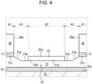
- the tapering surface 21a and the recessed surface 21b of the first immobilized layer 21 and the second immobilized layer 22 are positioned in the opening of the protective film 30. That is, the protective film 30 does not cover the tapering surface 21a and the recessed surface 21b of the first immobilized layer 21 and the upper surface 22a of the second immobilized layer 22.
- the sensor device 1 includes the unreacted antibodies 51 on the upper surface 22a of the second immobilized layer 22 in order to detect the antigens 61.
- the sensor device 1 may include, on the upper surface 22a of the second immobilized layer 22, another element, such as aptamers or enzymes, that can react with a detection target substance or can bind to the detection target substance.
- the sensor device 1 detect a change in the state of the vicinity of the upper surface 22a of the second immobilized layer 22 with high accuracy.
- the SAW 70 propagates in a region including the vicinity of the upper surface 22a of the second immobilized layer 22.
- the correlation between the propagation characteristics of the SAW 70 and the change in the state of the vicinity of the upper surface 22a of the second immobilized layer 22 becomes stronger.
- the waveguide 20 includes, in the upper surface thereof, the covered surface 21c of the first immobilized layer 21 that is covered by the protective film 30.
- a region including at least a part of the covered surface 21c of the first immobilized layer 21 is also called a "first region" and denoted by A1.
- the waveguide 20 includes, in the upper surface thereof, the upper surface 22a of the second immobilized layer 22 that is not covered by the protective film 30.
- a region including at least a part of the upper surface 22a of the second immobilized layer 22 is also called a "second region" and denoted by A2.
- the waveguide 20 includes, in the upper surface thereof, the tapering surface 21a of the first immobilized layer 21 and the recessed surface 21b on which the second immobilized layer 22 is not positioned.
- a region including at least a part of the tapering surface 21a of the first immobilized layer 21 and at least a part of the recessed surface 21b on which the second immobilized layer 22 is not positioned is also called a "third region" and denoted by A3.
- the SAW 70 propagates in the vicinity of the upper surface of the waveguide 20. As seen from the substrate surface 10a, the height of the third region is less than the height of the first region.
- the propagation characteristics of the SAW 70 in the waveguide 20 are based on the propagation characteristics of the first immobilized layer 21 and the propagation characteristics of the second immobilized layer 22. As the thickness of the first immobilized layer 21 and the second immobilized layer 22 becomes larger, the first immobilized layer 21 and the second immobilized layer 22 exert a greater effect on the propagation characteristics of the SAW 70 in the waveguide 20. That is, the sensitivity of the sensor device 1 can be controlled by controlling the aforementioned thickness. As seen from the substrate surface 10a, the height of the third region is less than the height of the second region.
- the energy of the SAW 70 can be concentrated on the vicinity of the surface of the second immobilized layer 22.
- the size of the second immobilized layer 22 in a direction that intersects the propagation direction of the SAW 70 is denoted by W3 in Fig. 2 .
- W3 has a length greater than or equal to W1 and W2. If W3 is shorter than W1 and W2, in the energy of the SAW 70 that propagates from the first IDT electrode 11 to the second IDT electrode 12, the proportion of the energy of the SAW 70 that propagates outside of the second immobilized layer 22 increases.
- the sensitivity in detection of a change in the state of the vicinity of the surface of the second immobilized layer 22 decreases.
- W3 has a length greater than or equal to W1 and W2
- the proportion of the energy of the SAW 70 that propagates outside of the second immobilized layer 22 can be reduced.
- the sensitivity in detection of a change in the state of the vicinity of the surface of the second immobilized layer 22 can be improved.
- W3 has a length greater than or equal to W1 and W2
- the SAW 70 can efficiently propagate from the first IDT electrode 11 to the second immobilized layer 22.
- the first reference electrode 11G and the first signal electrode 11A of the first IDT electrode 11 are each comb-shaped in a plan view.
- the first reference electrode 11G and the first signal electrode 11A each include two comb teeth.
- the electrodes 11G and 11A each may include one comb tooth or three or more comb teeth.
- the first reference electrode 11G and the first signal electrode 11A are alternately arranged in a direction from the waveguide 20 toward the first IDT electrode 11. Pairs each composed of one first reference electrode 11G and one first signal electrode 11A are arranged at a first pitch.
- the first IDT electrode 11 generates the SAW 70 along the surface of the substrate 10 based on an electric signal that is input to the first reference electrode 11G and the first signal electrode 11A.
- the wavelength of the SAW 70 generated by the first IDT electrode 11 corresponds to the first pitch.
- the second reference electrode 12G and the second signal electrode 12A of the second IDT electrode 12 are each comb-shaped in a plan view.
- the second reference electrode 12G and the second signal electrode 12A each include two comb teeth.
- the electrodes 12G and 12A each may include one comb tooth or three or more comb teeth.
- the second reference electrode 12G and the second signal electrode 12A are alternately arranged in a direction from the waveguide 20 toward the second IDT electrode 12. Pairs each composed of one second reference electrode 12G and one second signal electrode 12A are arranged at a second pitch.
- the second IDT electrode 12 outputs, to the second reference electrode 12G and the second signal electrode 12A, an electric signal based on the SAW 70 propagated from the first IDT electrode 11 through the waveguide 20.
- the efficiency with which the SAW 70 is converted into an electric signal by the second IDT electrode 12 increases.
- the sensor device 1 is configured in such a way that the first pitch and the second pitch coincide.
- the substrate-side close-contact layer 15, a metal layer 16, and the protective-film-side close-contact layer 17 are formed on the substrate surface 10a of the substrate 10.
- the substrate 10 is configured as illustrated in Fig. 5 . It is assumed that the substrate-side close-contact layer 15 and the protective-film-side close-contact layer 17 are made of titanium (Ti). It is assumed that the metal layer 16 is made of gold (Au).
- the first reference electrode 11G and the first signal electrode 11A, the second reference electrode 12G and the second signal electrode 12A, and the first immobilized layer 21 that constitutes the waveguide 20 are formed.
- the first reference electrode 11G and the first signal electrode 11A constitute the first IDT electrode 11.
- the second reference electrode 12G and the second signal electrode 12A constitute the second IDT electrode 12.
- the substrate 10 is configured as illustrated in Figs. 6 and 7 .
- the first reference electrode 11G, the first signal electrode 11A, the second reference electrode 12G, the second signal electrode 12A, and the first immobilized layer 21 may be formed by using any appropriate processing technology. For example, etching based on a mask having a desirable pattern may be used. The mask may be formed, for example, by photolithography. As the mask, a resist resin or the like may be used. The etching may include wet etching or dry etching. The wet etching may include a step of dissolving a material in an acid solution, an alkaline solution, or the like. The dry etching may include a step of removing a material by using plasma, such as reactive ion etching (RIE) or sputter etching.
- RIE reactive ion etching
- the first step and the second step may be replaced with a step of forming the first IDT electrode 11, the second IDT electrode 12, and the first immobilized layer 21 in a patterned state on the substrate surface 10a.
- the step of forming these in a patterned state can be realized, for example, by forming the substrate-side close-contact layer 15, the metal layer 16, and the protective-film-side close-contact layer 17 in a state of being covered by a hard mask made of a metal, a resist resin mask, or the like.
- the first IDT electrode 11, the second IDT electrode 12, and the first immobilized layer 21 are simultaneously formed.
- a step of forming the first IDT electrode 11 and the second IDT electrode 12 and a step of forming the first immobilized layer 21 may be divided as independent steps. When the steps are divided, whichever of the steps may be performed first.
- the position of the first immobilized layer 21 relative to the first IDT electrode 11 and the second IDT electrode 12 can be controlled with high accuracy.
- the distance from the first IDT electrode 11 and the second IDT electrode 12 to the first immobilized layer 21 is important.
- the present step because the position of the first immobilized layer 21 relative to the first IDT electrode 11 and the second IDT electrode 12 is controlled with high accuracy, it is possible to improve the accuracy of the distance and to improve the measurement accuracy.
- the protective film 30 for covering elements formed on the substrate surface 10a is formed.
- the substrate 10 is configured as illustrated in Fig. 8 . It is assumed that the protective film 30 is a TEOS oxide film.
- a part of the protective film 30 is removed.
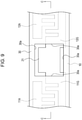
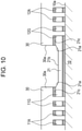
- the substrate 10 is configured as illustrated in Figs. 9 and 10 .
- the protective film 30 is removed to expose at least a part of the first immobilized layer 21 while leaving the first IDT electrode 11 and the second IDT electrode 12 to be covered. Because a part of the protective film 30 is removed, an opening surrounded by the side wall 30a is formed in the protective film 30. It can be said that the first immobilized layer 21 is exposed in the opening.
- the protective film 30 may be removed, for example, by etching based on a mask having a pattern of the opening. The etching may be performed by using any appropriate method.
- the opening in the protective film 30 is formed by etching such as dry etching or wet etching.
- the opening is formed by, for example, dry etching including sputtering, such as RIE.
- Sputtering can form the tapering surface 21a and the recessed surface 21b of the first immobilized layer 21, while forming the opening of the protective film 30.
- the tapering surface 21a and the recessed surface 21b of the first immobilized layer 21 are called an "exposed surface" of the first immobilized layer 21.
- the second immobilized layer 22 is formed.
- the substrate 10 is configured as illustrated in Figs. 2 and 3 .
- the second immobilized layer 22 may be formed in a desirable pattern by, for example, being formed in a state of being covered by a hard mask. In a case where the second immobilized layer 22 is patterned in the state of being covered by a mask, it becomes easier to maintain the state of the second immobilized layer 22 after being patterned to be the same as the state immediately after being formed, compared with a case where the immobilized layer is patterned by etching.
- patterning performed by forming a layer in a masked state is less likely to exert an effect on the second immobilized layer 22 than patterning performing by etching. That is, the surface of the second immobilized layer 22 is regulated further than the surface of the first immobilized layer 21, and it is easier to immobilize antibodies on the surface of the second immobilized layer 22 than on the surface of the first immobilized layer 21.
- the thickness of the second immobilized layer 22 increases, the thickness of the waveguide 20, including the first immobilized layer 21 and the second immobilized layer 22, increases.
- the thickness of the waveguide 20 exerts an effect on the sensitivity of the sensor device 1.
- a substance such as antibodies, aptamers, or enzymes, that reacts with a detection target is immobilized on the upper surface 22a of the second immobilized layer 22.
- the unreacted antibodies 51 see Fig. 1
- the unreacted antibodies 51 are immobilized on the upper surface of the waveguide 20.
- the second immobilized layer 22 is made of gold (Au)
- the antibodies may be formed, for example, on the surface of the second immobilized layer 22 based on a gold thiol bond, which is a bond between gold (Au) and divalent sulfur (S).
- a polymer film is formed on the surface of the second immobilized layer 22, and antibodies may be bound to the polymer by amine coupling by using an appropriate condensation agent (such as EDC/NHS reagent) in the polymer film.
- the antibodies may be immobilized on the second immobilized layer 22 by being bound to the polymer film.
- the state of the upper surface 22a of the second immobilized layer 22 can exert an effect on immobilization of the antibodies.
- a surface state such as the composition and the surface roughness of the upper surface 22a can exert an effect as to whether or not the antibodies can be easily immobilized on the upper surface 22a.
- the state of the second immobilized layer 22 can exert an effect on immobilization of the antibodies to the upper surface. In order to control the sensitivity of the sensor device 1 with high accuracy, it is required to control the state of the second immobilized layer 22 on which the unreacted antibodies 51 are to be immobilized.
- the unreacted antibodies 51 are immobilized on the recessed surface 21b of the first immobilized layer 21.
- the state of the recessed surface 21b is changed due to etching of the protective film 30. Etching includes many uncertain factors. Accordingly, it is difficult to control the change in the state of a surface due to etching. For example, the surface roughness of the recessed surface 21b changes due to etching. However, it is difficult to control the surface roughness.
- the second immobilized layer 22 is formed.
- the state of the upper surface 22a of the second immobilized layer 22 can be controlled more easily than the state of the recessed surface 21b of the first immobilized layer 21.
- the surface roughness of the upper surface 22a can be controlled by controlling the film-forming conditions of the second immobilized layer 22. In general, it is easier to control the surface roughness by film-forming than to control the surface roughness by etching. Accordingly, it becomes easier to immobilize the unreacted antibodies 51 on the upper surface 22a of the second immobilized layer 22. As a result, it becomes easier to control the sensitivity of the sensor device 1.
- the sensor device 1 according to the present embodiment may be manufactured by performing each of the aforementioned steps.
- the aforementioned steps are each an example. Any appropriate step may be added. Some of the steps may be omitted.
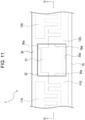
- the second immobilized layer 22 may be positioned on the side wall 30a of the protective film 30.
- the second immobilized layer 22 may be positioned further outside as seen from the opening formed in the side wall 30a. That is, end portions of the second immobilized layer 22 that are respectively adjacent to the first IDT electrode 11 and the second IDT electrode 12 are positioned on the upper side of the protective film 30.
- the protective film 30 covers the covered surfaces 21c that are positioned respectively adjacent to the first IDT electrode 11 and the second IDT electrode 12. That is, the protective film 30 covers end portions of the first immobilized layer 21 that are respectively adjacent to the first IDT electrode 11 and the second IDT electrode 12.
- the waveguide 20 may further include the third immobilized layer 23 between the recessed surface 21b of the first immobilized layer 21 and the second immobilized layer 22.
- the third immobilized layer 23 can improve the closeness of contact between the second immobilized layer 22 and the first immobilized layer 21.
- the third immobilized layer 23 may be made of, for example, titanium (Ti), chrome (Cr), or the like.
- the material of the third immobilized layer 23 is not limited to these, and may be a material having high closeness of contact between the first immobilized layer 21 and the second immobilized layer 22. When the closeness of contact between the first immobilized layer 21 and the second immobilized layer 22 increases, the reliability of the sensor device 1 can be improved.
- the protective film 30 need not cover the waveguide 20, although the protective film 30 covers the first IDT electrode 11 and the second IDT electrode 12. That is, the side wall 30a of the protective film 30 may be positioned between the first IDT electrode 11 and the second IDT electrode 12 and the waveguide 20.
- the waveguide 20 includes the first immobilized layer 21 and the second immobilized layer 22.
- the first immobilized layer 21 has an upper surface 21d.
- the second immobilized layer 22 has the upper surface 22a, and is positioned on the upper surface 21d of the first immobilized layer 21.
- the second immobilized layer 22 has the contact surface 22b on a side facing the substrate surface 10a.
- the contact surface 22b is in contact with a part of the upper surface 21d of the first immobilized layer 21.
- the second immobilized layer 22 may be positioned to cover a half or more of the upper surface 21d of the first immobilized layer 21.
- the waveguide 20 may include the third immobilized layer 23 (see Fig. 13 ) between the first immobilized layer 21 and the second immobilized layer 22.
- the second immobilized layer 22 can be formed in a step different from a step of forming the first immobilized layer 21.
- ordinal numbers such as “first” and “second” are identifiers for discriminating between the elements.
- the ordinal numbers may be replaced with each other.
- the identifiers "first” and “second” of the first phosphor and the second phosphor may be replaced with each other. Replacement of the identifiers is performed simultaneously. Even after the replacement of identifiers, the elements are discriminated.
- the identifiers may be omitted. Elements from which the identifiers are omitted are discriminated by reference numerals.
- the identifiers "first", “second”, and the like should not be used for the interpretation of the order of the elements and as the basis for the presence of an identifier with a smaller number.
Landscapes
- Physics & Mathematics (AREA)
- Biochemistry (AREA)
- Health & Medical Sciences (AREA)
- Life Sciences & Earth Sciences (AREA)
- Chemical & Material Sciences (AREA)
- Analytical Chemistry (AREA)
- General Health & Medical Sciences (AREA)
- General Physics & Mathematics (AREA)
- Immunology (AREA)
- Pathology (AREA)
- Acoustics & Sound (AREA)
- Investigating Or Analyzing Materials By The Use Of Ultrasonic Waves (AREA)
- Surface Acoustic Wave Elements And Circuit Networks Thereof (AREA)
Abstract
Description
- The present application claims priority of
Japanese Patent Application No. 2019-86563, filed on April 26, 2019 - The present disclosure relates to a method of manufacturing a sensor device and a sensor device.
- A known surface acoustic wave device has a configuration in which an electrode that generates a surface acoustic wave is covered by a film (see, for example, PTL 1) .
- PTL 1:
Japanese Unexamined Patent Application Publication No. 2017-28543 - A sensor device according to an embodiment of the present disclosure includes a substrate having a substrate surface, a first IDT electrode positioned on the substrate surface, a second IDT electrode positioned on the substrate surface, a waveguide, and a protective film. The waveguide is positioned on the substrate surface and between the first IDT electrode and the second IDT electrode. The waveguide includes a first immobilized layer positioned on the substrate surface and a second immobilized layer positioned on the first immobilized layer. The second immobilized layer is positioned inside an outer edge of the first immobilized layer as seen in a plan view.
- A method of manufacturing a sensor device according to an embodiment of the present disclosure includes a step of forming a metal layer on a substrate. The method includes a step of removing a part of the metal layer to form a first IDT electrode, a second IDT electrode, and a first immobilized layer positioned between the first IDT electrode and the second IDT electrode. The method includes a step of forming a protective film that covers the first IDT electrode, the second IDT electrode, and the first immobilized layer. The method includes a step of removing a part of the protective film to expose at least a part of the first immobilized layer. The method includes a step of forming a second immobilized layer on at least a part of an exposed surface of the first immobilized layer.
-
- [
Fig. 1] Fig. 1 is a schematic view of a sensor device according to an embodiment. - [
Fig. 2] Fig. 2 is a plan view of the sensor device according to the embodiment. - [
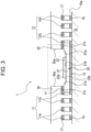
Fig. 3] Fig. 3 is a sectional view taken along line A-A ofFig. 2 . - [
Fig. 4] Fig. 4 is an enlarged view of a region surrounded by a two-dot chain line inFig. 3 . - [
Fig. 5] Fig. 5 is a sectional view of a substrate on which a first step of a method of manufacturing a sensor device has been performed. - [
Fig. 6] Fig. 6 is a plan view of the substrate on which a second step of the method of manufacturing a sensor device has been performed. - [
Fig. 7] Fig. 7 is a sectional view taken along line B-B inFig. 6 . - [
Fig. 8] Fig. 8 is a sectional view of the substrate on which a third step of the method of manufacturing a sensor device has been performed. - [
Fig. 9] Fig. 9 is a plan view of the substrate on which a fourth step of the method of manufacturing a sensor device has been performed. - [
Fig. 10] Fig. 10 is a sectional view taken along line C-C inFig. 9 . - [
Fig. 11] Fig. 11 is a sectional view illustrating an example of a configuration in which a second immobilized layer is positioned also on the upper side of a protective film. - [
Fig. 12] Fig. 12 is a sectional view taken along line D-D inFig. 11 . - [
Fig. 13] Fig. 13 is a sectional view illustrating an example of a configuration in which a waveguide includes a third immobilized layer. - [
Fig. 14] Fig. 14 is a sectional view illustrating an example of a configuration in which a first IDT electrode, a second IDT electrode, and a waveguide are separated from each other. - A surface acoustic wave device detects a change in a state on a waveguide by detecting a propagation state of a surface acoustic wave. It is required to improve the accuracy in detection of the change in the state on the waveguide.
- A sensor device 1 (see
Fig. 1 ) according to an embodiment of the present disclosure and a method of manufacturing thesensor device 1 can improve the accuracy in detection of a surface state of a waveguide. - As illustrated in
Fig. 1 , thesensor device 1 according to the embodiment includes asubstrate 10, a first IDT (interdigital transducer)electrode 11, asecond IDT electrode 12, and awaveguide 20. Thesensor device 1 functions as a SAW sensor that can detect a change in the propagation characteristics of a surface acoustic wave (SAW) 70. Thesensor device 1 inputs an alternate-current electric signal to thefirst IDT electrode 11. Thefirst IDT electrode 11 generates the SAW 70 along a surface of thesubstrate 10 based on the input electric signal. The SAW 70 propagates from thefirst IDT electrode 11 to thesecond IDT electrode 12. The propagation path from thefirst IDT electrode 11 to thesecond IDT electrode 12 includes a surface of thesubstrate 10 and thewaveguide 20 positioned on the surface of thesubstrate 10. That is, the SAW 70 propagates from thefirst IDT electrode 11 to thesecond IDT electrode 12 via thesubstrate 10 and thewaveguide 20. Thesecond IDT electrode 12 outputs an electric signal based on the SAW 70 propagated from thefirst IDT electrode 11. The electric signal may include a voltage signal or a current signal. It can be said that thefirst IDT electrode 11 transmits theSAW 70 toward thewaveguide 20 and thesecond IDT electrode 12. It can be said thesecond IDT electrode 12 receives theSAW 70 from thefirst IDT electrode 11 and thewaveguide 20. - The SAW 70 propagates with predetermined propagation characteristics. The propagation characteristics of the
SAW 70 are determined based on the state of the propagation path. Thesensor device 1 can detect a change in the state of the propagation path by detecting a change in the propagation characteristics of theSAW 70. The propagation characteristics include, for example, a propagation velocity. Thesensor device 1 can detect a change in the propagation velocity as a change in the phase difference between an electric signal input to thefirst IDT electrode 11 and an electric signal output from thesecond IDT electrode 12. An electric signal input to thefirst IDT electrode 11 is also called an "input signal". An electric signal output from thesecond IDT electrode 12 is also called an "output signal". That is, thesensor device 1 can detect a change in the state of the propagation path based on a change in the phase difference between the input signal and the output signal. - In the
sensor device 1 according to the present embodiment, the SAW 70 propagates through thewaveguide 20 from thefirst IDT electrode 11 to thesecond IDT electrode 12. Accordingly, the state of the propagation path of the SAW 70 is determined based on the state of thewaveguide 20. - The state of the
waveguide 20 may be specified, for example, by a parameter such as: a mass on a surface of thewaveguide 20 or of the vicinity of the surface; or the density, the viscosity, or the like of a substance that is present on the surface or in the vicinity of the surface. The mass, the density, the viscosity, or the like can exert an effect on the propagation characteristics of the SAW 70. - When the
sensor device 1 detects a change in the phase difference between an input signal and an output signal, thesensor device 1 can calculate a change in the state of the vicinity of the surface of thewaveguide 20 based on the detection result. For example, when a change in the mass of the vicinity of the surface of thewaveguide 20 causes a change in the propagation characteristics of theSAW 70 and a change in the phase difference between an input signal and an output signal, thesensor device 1 can calculate the change in the mass of the vicinity of the surface of thewaveguide 20. In this case, a calibration curve that specifies the relationship between the amount of change in the phase difference and the amount of change in the mass of the vicinity of the surface of thewaveguide 20 may be prepared beforehand. Thesensor device 1 may convert the amount of change in the phase difference into an amount of change of the mass of the vicinity of the surface of thewaveguide 20 or the like based on the calibration curve. - The
sensor device 1 illustrated inFig. 1 includes a first channel including a pair of a first IDT electrode 11-1 and a second IDT electrode 12-1 and a waveguide 20-1. Thesensor device 1 illustrated inFig. 1 includes a second channel including a pair of a first IDT electrode 11-2 and a second IDT electrode 12-2 and a waveguide 20-2. The number of channels of thesensor device 1 is not limited to two, and may be one, or three or more. - The
sensor device 1 detects the phase difference between an input signal and an output signal in each of the first channel and the second channel. The phase differences detected in the first channel and the second channel will be called a "first phase difference" and a "second phase difference", respectively. The phase difference between an input signal and an output signal is based on the propagation velocity of theSAW 70 and the distance from thefirst IDT electrode 11 to thesecond IDT electrode 12. If the propagation velocities of theSAW 70 in the first channel and the second channel are the same, the first phase difference is equal to the second phase difference. If the propagation velocities of theSAW 70 in the first channel and the second channel are different, the first phase difference and the second phase difference differ from each other, unless the propagation time of theSAW 70 coincides with an integer multiple of the period of theSAW 70. - The waveguide 20-2 of the second channel includes antibodies on a surface thereof. The antibodies react with
specific antigens 61 to be detected. Antibodies that have not reacted with theantigens 61 are called "unreacted antibodies 51". Antibodies that have reacted with theantigens 61 are called "reactedantibodies 52". It is assumed that thewaveguide 20 of the second channel includes theunreacted antibodies 51 and the reactedantibodies 52 on the surface thereof. The reactedantibodies 52 of thewaveguide 20 of the second channel can be generated by reaction between theunreacted antibodies 51 that have been originally present on the surface of thewaveguide 20 and theantigens 61 included in aspecimen 60 introduced into thewaveguide 20. On the other hand, it is assumed that the waveguide 20-1 of the first channel does not include antigens on the surface thereof. - The reacted
antibodies 52 have bound to theantigens 61. Because the reactedantibodies 52 have bound theantigens 61, the mass of the vicinity of the surface of thewaveguide 20 is greater than the mass of theunreacted antibodies 51 by the amount of theantigens 61 with which the reactedantibodies 52 have reacted. Accordingly, as the proportion of the reactedantibodies 52 to the antibodies included in the waveguide 20-2 increases, the mass of the vicinity of the surface of the waveguide 20-2 of the second channel increases. That is, the state of the propagation path of the second channel changes in accordance with the change in the proportion of the reactedantibodies 52. - The antibodies may be replaced with aptamers. The aptamers include nucleic acid molecules, peptides, and the like that specifically bind to specific molecules to be detected. When the
waveguide 20 includes aptamers on the surface thereof, the mass of the vicinity of the surface of thewaveguide 20 increases as the aptamers bind to the specific molecules. The antibodies may be replaced with enzymes. As the enzymes form complexes with specific molecules, the mass increases. The antibodies are not may be replaced with, instead of these examples, another element that can react with a substance to be detected or that can bind to a substance to be detected. Thewaveguide 20 having an element, such as antibodies, that can react with or bind to a detection target substance, is also called a "reaction unit". - The first channel of the
sensor device 1 allows theSAW 70 to propagate through thewaveguide 20 and detects the first phase difference. The first phase difference is used as a reference value of a phase difference detected by thesensor device 1. The second channel of thesensor device 1 allows theSAW 70 to propagate through thewaveguide 20 including theunreacted antibodies 51 or the reactedantibodies 52 and detects the second phase difference. The second phase difference is determined by the proportion of the reactedantibodies 52 to the antibodies included in thewaveguide 20. Thesensor device 1 may correct the result of detection of the second phase difference by using the first phase difference as a reference value. Thesensor device 1 may calculate the amount of theantigens 61 bound by the antibodies of the waveguide 20-2 of the second channel based on the result of detection of the second phase difference. A calibration curve that specifies the relationship between the amount of change in the second phase difference and the amount of theantigens 61 may be prepared beforehand. Thesensor device 1 may covert the amount of change in the second phase difference into the amount, the concentration, the density, or the like of theantigens 61 based on the calibration curve. As a result, thesensor device 1 can detect a detection target included in thespecimen 60. - The
specimen 60 may include, for example, human blood, urine, saliva, or the like. Thespecimen 60 is not limited to this, and may include any appropriate chemical substance. Thespecimen 60 may be preprocessed before thespecimen 60 is introduced into a channel of thesensor device 1. - The reaction through which the
unreacted antibodies 51 bind to theantigens 61 to become the reactedantibodies 52 progresses with a predetermined reaction velocity. Accordingly, in accordance with the elapsed time after introduction of thespecimen 60 into the channel, the proportion of the reactedantibodies 52 to the antibodies included in thewaveguide 20 increases, and can gradually approach the proportion of the antigen concentration. As a result, the phase difference that thesensor device 1 detects in the channel changes in accordance with the elapsed time, and can gradually approach a predetermined phase difference. The amount of the reactedantibodies 52 in the antibodies included in thewaveguide 20 can saturate when the reaction between theantigens 61 and theunreacted antibodies 51 almost finishes. Thesensor device 1 may calculate the amount of theantigens 61 based on the phase difference that is detected after an elapse of a sufficiently long time since the introduction of thespecimen 60 into the channel. - The
sensor device 1 may detect a period of time from input of an electric signal to thefirst IDT electrode 11 to detection of the electric signal by thesecond IDT electrode 12. Thesensor device 1 may detect a change in the state of the vicinity of the surface of thewaveguide 20 by detecting a change in the propagation velocity by calculating the propagation velocity based on the period of time from input of the electric signal to detection of the electric signal and the distance between the electrodes. Note that thesensor device 1 may detect, as propagation characteristics, a change in the amplitude of theSAW 70 or a plurality of characteristics. - Referring to
Figs. 2 ,3 , and4 , each element of thesensor device 1 will be described in further detail. As described above, thesensor device 1 includes thesubstrate 10, thefirst IDT electrode 11, thesecond IDT electrode 12, and thewaveguide 20. Thesensor device 1 further includes aprotective film 30. - The
substrate 10 has asubstrate surface 10a. It is assumed that thesubstrate 10 is a quartz substrate. However, thesubstrate 10 is not limited to this, and may be made of another material, such as piezoelectric ceramics, that causes a piezoelectric phenomenon. - The
first IDT electrode 11 and thesecond IDT electrode 12 are positioned on thesubstrate surface 10a. Thefirst IDT electrode 11 and thesecond IDT electrode 12 may be made of a metal such as gold (Au) or aluminum (Al). Thefirst IDT electrode 11 and thesecond IDT electrode 12 may be made of, instead of gold (Au) or aluminum (Al), any other appropriate material such as an alloy (AlCu) of aluminum (Al) and copper (Cu). - The
first IDT electrode 11 and thesecond IDT electrode 12 may have a substrate-side close-contact layer 15 between thefirst IDT electrode 11 and thesecond IDT electrode 12 and thesubstrate surface 10a. Thefirst IDT electrode 11 and thesecond IDT electrode 12 may have a protective-film-side close-contact layer 17 between theprotective film 30 and surfaces thereof on a side opposite to a side facing thesubstrate surface 10a. The substrate-side close-contact layer 15 and the protective-film-side close-contact layer 17 may be made of, for example, titanium (Ti), chrome (Cr), or the like, but may be made of, instead of these, any other appropriate material. The substrate-side close-contact layer 15 and the protective-film-side close-contact layer 17 may be made of different materials. - The
first IDT electrode 11 includes afirst reference electrode 11G and afirst signal electrode 11A to which a voltage is to be applied. Thesensor device 1 generates theSAW 70 in thefirst IDT electrode 11 by applying a voltage signal between thefirst reference electrode 11G and thefirst signal electrode 11A. Thefirst reference electrode 11G may be connected to a ground point. TheSAW 70 is generated between thefirst reference electrode 11G and thefirst signal electrode 11A. The distance between thefirst reference electrode 11G and thefirst signal electrode 11A is denoted by W1. Within the range of a length denoted by W1, theSAW 70 has energy higher than that in the other ranges. - The
second IDT electrode 12 includes asecond reference electrode 12G and asecond signal electrode 12A to which a voltage is to be applied. Thesensor device 1 detects an electric signal generated by the propagatedSAW 70 by using thesecond reference electrode 12G and thesecond signal electrode 12A. Thesecond reference electrode 12G may be connected to a ground point. TheSAW 70 propagates between thesecond reference electrode 12G and thesecond signal electrode 12A. The distance between thesecond reference electrode 12G and thesecond signal electrode 12A is denoted by W2. TheSAW 70 propagated to the range of a length denoted by W2 generates in thesecond IDT electrode 12 an electric signal that is greater than that generated by theSAW 70 propagated to the other ranges. That is, thesecond IDT electrode 12 can efficiently detect theSAW 70 in the range denoted by W2. - The
waveguide 20 is positioned on thesubstrate surface 10a and between thefirst IDT electrode 11 and thesecond IDT electrode 12. Thewaveguide 20 includes a first immobilizedlayer 21 and a second immobilizedlayer 22. - The first
immobilized layer 21 is positioned on thesubstrate surface 10a. It is regarded that the first immobilizedlayer 21, thefirst reference electrode 11G, and thesecond reference electrode 12G are integrally formed, although they are divided inFigs. 2 and3 for convenience of description. In the following other figures, it is regarded that the first immobilizedlayer 21, thefirst reference electrode 11G, and thesecond reference electrode 12G are integrally formed, even though they are described below as if being divided. The firstimmobilized layer 21, thefirst reference electrode 11G, and thesecond reference electrode 12G may be treated as independent elements for convenience of description, although they are not divided in the description thereof. When the first immobilizedlayer 21 is integrally formed with thefirst reference electrode 11G and thesecond reference electrode 12G, the first immobilizedlayer 21 is made of a material that is the same as the material of thefirst reference electrode 11G and thesecond reference electrode 12G. The firstimmobilized layer 21 may be made of, for example, gold (Au). Thewaveguide 20 comes into contact with thespecimen 60. The firstimmobilized layer 21 may be made of, instead of gold (Au), another material that has oxidation resistance and corrosion resistance against contact with thespecimen 60. When the first immobilizedlayer 21 is integrally formed with thefirst reference electrode 11G and thesecond reference electrode 12G, the electric potential of thewaveguide 20 is the same as the electric potential of thefirst reference electrode 11G and thesecond reference electrode 12G. - The first
immobilized layer 21 may be formed as an independent member separate from thefirst reference electrode 11G and thesecond reference electrode 12G by a predetermined distance. When the first immobilizedlayer 21 is formed an independent member separate from thefirst reference electrode 11G and thesecond reference electrode 12G, the first immobilizedlayer 21 may be made of a material that is the same as or different from the material of thefirst reference electrode 11G and thesecond reference electrode 12G. The firstimmobilized layer 21 may be made of, for example, gold (Au) or another material that has oxidation resistance and corrosion resistance against contact with thespecimen 60. When the first immobilizedlayer 21 is integrally formed with thefirst reference electrode 11G and thesecond reference electrode 12G, the electric potential of thewaveguide 20 may be the same as the electric potential of at least one of thefirst reference electrode 11G and thesecond reference electrode 12G. The electric potential of thewaveguide 20 may be a floating potential. - The first
immobilized layer 21 may have the substrate-side close-contact layer 15 between the first immobilizedlayer 21 and thesubstrate surface 10a. The substrate-side close-contact layer 15 of the first immobilizedlayer 21 may be formed integrally with or separate from the substrate-side close-contact layer 15 of thefirst IDT electrode 11 and thesecond IDT electrode 12. - The first
immobilized layer 21 has an upper surface on a side opposite to a side facing thesubstrate surface 10a. The upper surface of the first immobilizedlayer 21 may include atapering surface 21a, a recessedsurface 21b, and a coveredsurface 21c. The firstimmobilized layer 21 may have the protective-film-side close-contact layer 17 between the coveredsurface 21c and theprotective film 30. The height of the recessedsurface 21b as seen from thesubstrate surface 10a is less than or equal to the height of the coveredsurface 21c. The taperingsurface 21a is positioned between the recessedsurface 21b and the coveredsurface 21c and is inclined at a predetermined angle with respect to thesubstrate surface 10a. - The second
immobilized layer 22 has anupper surface 22a, and is positioned on the upper surface of the first immobilizedlayer 21. In a plan view of thesubstrate 10, the second immobilizedlayer 22 may be positioned inside an outer edge of the upper surface of the first immobilizedlayer 21. The secondimmobilized layer 22 may have acontact surface 22b on a side facing thesubstrate surface 10a. Thecontact surface 22b may be in direct contact with a part of the upper surface of the first immobilizedlayer 21. When a third immobilized layer 23 is positioned between the first immobilizedlayer 21 and the second immobilizedlayer 22 as described below, thecontact surface 22b may be in contact with a part of the upper surface of the first immobilizedlayer 21 via the third immobilized layer 23. In other words, thecontact surface 22b may face a part of the upper surface of the first immobilizedlayer 21 via the third immobilized layer 23, while being in contact with the third immobilized layer 23. In a plan view of thesubstrate 10, thecontact surface 22b may be positioned inside the outer edge of the upper surface of the first immobilizedlayer 21. The secondimmobilized layer 22 may be positioned in the range of the recessedsurface 21b. That is, the second immobilizedlayer 22 may be positioned not to overlap the taperingsurface 21a. A part of the second immobilizedlayer 22 may be positioned on the taperingsurface 21a. The secondimmobilized layer 22 may be positioned to cover a half or more of the upper surface of the first immobilizedlayer 21. As described below, thewaveguide 20 may include the third immobilized layer 23 (seeFig. 13 ) between the first immobilizedlayer 21 and the second immobilizedlayer 22. When thewaveguide 20 does not include the third immobilized layer 23, the first immobilizedlayer 21 and the second immobilizedlayer 22 can be discriminated from each other by using any appropriate analysis method. As the analysis method, for example, a scanning electron microscope (SEM), a transmission electron microscope (TEM), or the like may be used, or another method may be used. - The second
immobilized layer 22 may be made of, for example, gold (Au). The secondimmobilized layer 22 may be made of, instead of gold (Au), another material that has oxidation resistance and corrosion resistance against contact with thespecimen 60. The secondimmobilized layer 22 may be made of a material that is the same as the material of the first immobilizedlayer 21 or a material that is different from the material of the first immobilizedlayer 21. The surface roughness of theupper surface 22a of the second immobilizedlayer 22 may be different from the surface roughness of the upper surface of the first immobilizedlayer 21. The surface roughness of theupper surface 22a of the second immobilizedlayer 22 may be less than the surface roughness of the upper surface of the first immobilizedlayer 21. The thickness of the second immobilizedlayer 22 may be different from the thickness of the first immobilizedlayer 21. The thickness of the second immobilizedlayer 22 may be less than the thickness of the first immobilizedlayer 21. - The
protective film 30 covers thesubstrate surface 10a, thefirst IDT electrode 11, thesecond IDT electrode 12, and the coveredsurface 21c of the first immobilizedlayer 21. Theprotective film 30 covers the coveredsurfaces 21c that are respectively positioned adjacent to thefirst IDT electrode 11 and thesecond IDT electrode 12. That is, theprotective film 30 covers end portions of thewaveguide 20 that are respectively adjacent to thefirst IDT electrode 11 and thesecond IDT electrode 12. - The
protective film 30 may be a TEOS oxide film. The TEOS oxide film is a silicon oxide film formed by using a plasma chemical vapor deposition (CVD) method in which tetraethoxysilane is used as a material gas. Theprotective film 30 is not limited to the TEOS oxide film, and may be made of another insulating material. Theprotective film 30 includes aside wall 30a that intersects thesubstrate surface 10a. Theside wall 30a defines an opening of theprotective film 30. The taperingsurface 21a and the recessedsurface 21b of the first immobilizedlayer 21 and the second immobilizedlayer 22 are positioned in the opening of theprotective film 30. That is, theprotective film 30 does not cover thetapering surface 21a and the recessedsurface 21b of the first immobilizedlayer 21 and theupper surface 22a of the second immobilizedlayer 22. - The
sensor device 1 includes theunreacted antibodies 51 on theupper surface 22a of the second immobilizedlayer 22 in order to detect theantigens 61. Thesensor device 1 may include, on theupper surface 22a of the second immobilizedlayer 22, another element, such as aptamers or enzymes, that can react with a detection target substance or can bind to the detection target substance. - It is required that the
sensor device 1 detect a change in the state of the vicinity of theupper surface 22a of the second immobilizedlayer 22 with high accuracy. TheSAW 70 propagates in a region including the vicinity of theupper surface 22a of the second immobilizedlayer 22. As a larger amount of energy of theSAW 70, which propagates in the second immobilizedlayer 22, is distributed in the vicinity of theupper surface 22a, the correlation between the propagation characteristics of theSAW 70 and the change in the state of the vicinity of theupper surface 22a of the second immobilizedlayer 22 becomes stronger. - As illustrated in
Fig. 4 , thewaveguide 20 includes, in the upper surface thereof, the coveredsurface 21c of the first immobilizedlayer 21 that is covered by theprotective film 30. A region including at least a part of the coveredsurface 21c of the first immobilizedlayer 21 is also called a "first region" and denoted by A1. Thewaveguide 20 includes, in the upper surface thereof, theupper surface 22a of the second immobilizedlayer 22 that is not covered by theprotective film 30. A region including at least a part of theupper surface 22a of the second immobilizedlayer 22 is also called a "second region" and denoted by A2. Thewaveguide 20 includes, in the upper surface thereof, the taperingsurface 21a of the first immobilizedlayer 21 and the recessedsurface 21b on which the second immobilizedlayer 22 is not positioned. A region including at least a part of the taperingsurface 21a of the first immobilizedlayer 21 and at least a part of the recessedsurface 21b on which the second immobilizedlayer 22 is not positioned is also called a "third region" and denoted by A3. - The
SAW 70 propagates in the vicinity of the upper surface of thewaveguide 20. As seen from thesubstrate surface 10a, the height of the third region is less than the height of the first region. - The propagation characteristics of the
SAW 70 in thewaveguide 20 are based on the propagation characteristics of the first immobilizedlayer 21 and the propagation characteristics of the second immobilizedlayer 22. As the thickness of the first immobilizedlayer 21 and the second immobilizedlayer 22 becomes larger, the first immobilizedlayer 21 and the second immobilizedlayer 22 exert a greater effect on the propagation characteristics of theSAW 70 in thewaveguide 20. That is, the sensitivity of thesensor device 1 can be controlled by controlling the aforementioned thickness. As seen from thesubstrate surface 10a, the height of the third region is less than the height of the second region. - The energy of the
SAW 70 can be concentrated on the vicinity of the surface of the second immobilizedlayer 22. The size of the second immobilizedlayer 22 in a direction that intersects the propagation direction of theSAW 70 is denoted by W3 inFig. 2 . W3 has a length greater than or equal to W1 and W2. If W3 is shorter than W1 and W2, in the energy of theSAW 70 that propagates from thefirst IDT electrode 11 to thesecond IDT electrode 12, the proportion of the energy of theSAW 70 that propagates outside of the second immobilizedlayer 22 increases. As the proportion of the energy of theSAW 70 that propagates outside of the second immobilizedlayer 22 increases, the sensitivity in detection of a change in the state of the vicinity of the surface of the second immobilizedlayer 22 decreases. When W3 has a length greater than or equal to W1 and W2, the proportion of the energy of theSAW 70 that propagates outside of the second immobilizedlayer 22 can be reduced. In this case, the sensitivity in detection of a change in the state of the vicinity of the surface of the second immobilizedlayer 22 can be improved. When W3 has a length greater than or equal to W1 and W2, theSAW 70 can efficiently propagate from thefirst IDT electrode 11 to the second immobilizedlayer 22. - The
first reference electrode 11G and thefirst signal electrode 11A of thefirst IDT electrode 11 are each comb-shaped in a plan view. In thesensor device 1 illustrated inFig. 2 , thefirst reference electrode 11G and thefirst signal electrode 11A each include two comb teeth. However, theelectrodes first reference electrode 11G and thefirst signal electrode 11A are alternately arranged in a direction from thewaveguide 20 toward thefirst IDT electrode 11. Pairs each composed of onefirst reference electrode 11G and onefirst signal electrode 11A are arranged at a first pitch. As described above, thefirst IDT electrode 11 generates theSAW 70 along the surface of thesubstrate 10 based on an electric signal that is input to thefirst reference electrode 11G and thefirst signal electrode 11A. The wavelength of theSAW 70 generated by thefirst IDT electrode 11 corresponds to the first pitch. - The
second reference electrode 12G and thesecond signal electrode 12A of thesecond IDT electrode 12 are each comb-shaped in a plan view. In thesensor device 1 illustrated inFig. 2 , thesecond reference electrode 12G and thesecond signal electrode 12A each include two comb teeth. However, theelectrodes second reference electrode 12G and thesecond signal electrode 12A are alternately arranged in a direction from thewaveguide 20 toward thesecond IDT electrode 12. Pairs each composed of onesecond reference electrode 12G and onesecond signal electrode 12A are arranged at a second pitch. As described above, thesecond IDT electrode 12 outputs, to thesecond reference electrode 12G and thesecond signal electrode 12A, an electric signal based on theSAW 70 propagated from thefirst IDT electrode 11 through thewaveguide 20. As the wavelength of theSAW 70 becomes closer to the second pitch, the efficiency with which theSAW 70 is converted into an electric signal by thesecond IDT electrode 12 increases. In other words, as the difference between the first pitch and the second pitch becomes smaller, the efficiency with which theSAW 70 is converted into an electric signal by thesecond IDT electrode 12 increases. In the present embodiment, thesensor device 1 is configured in such a way that the first pitch and the second pitch coincide. - Referring to
Figs. 2 to 10 , a method of manufacturing thesensor device 1 will be described. - In a first step, the substrate-side close-
contact layer 15, ametal layer 16, and the protective-film-side close-contact layer 17 are formed on thesubstrate surface 10a of thesubstrate 10. As a result of performing the first step, thesubstrate 10 is configured as illustrated inFig. 5 . It is assumed that the substrate-side close-contact layer 15 and the protective-film-side close-contact layer 17 are made of titanium (Ti). It is assumed that themetal layer 16 is made of gold (Au). - In a second step, the
first reference electrode 11G and thefirst signal electrode 11A, thesecond reference electrode 12G and thesecond signal electrode 12A, and the first immobilizedlayer 21 that constitutes thewaveguide 20 are formed. Thefirst reference electrode 11G and thefirst signal electrode 11A constitute thefirst IDT electrode 11. Thesecond reference electrode 12G and thesecond signal electrode 12A constitute thesecond IDT electrode 12. As a result of performing the second step, thesubstrate 10 is configured as illustrated inFigs. 6 and7 . - The
first reference electrode 11G, thefirst signal electrode 11A, thesecond reference electrode 12G, thesecond signal electrode 12A, and the first immobilizedlayer 21 may be formed by using any appropriate processing technology. For example, etching based on a mask having a desirable pattern may be used. The mask may be formed, for example, by photolithography. As the mask, a resist resin or the like may be used. The etching may include wet etching or dry etching. The wet etching may include a step of dissolving a material in an acid solution, an alkaline solution, or the like. The dry etching may include a step of removing a material by using plasma, such as reactive ion etching (RIE) or sputter etching. - The first step and the second step may be replaced with a step of forming the
first IDT electrode 11, thesecond IDT electrode 12, and the first immobilizedlayer 21 in a patterned state on thesubstrate surface 10a. The step of forming these in a patterned state can be realized, for example, by forming the substrate-side close-contact layer 15, themetal layer 16, and the protective-film-side close-contact layer 17 in a state of being covered by a hard mask made of a metal, a resist resin mask, or the like. - In the first step and the second step, the
first IDT electrode 11, thesecond IDT electrode 12, and the first immobilizedlayer 21 are simultaneously formed. A step of forming thefirst IDT electrode 11 and thesecond IDT electrode 12 and a step of forming the first immobilizedlayer 21 may be divided as independent steps. When the steps are divided, whichever of the steps may be performed first. When thefirst IDT electrode 11, thesecond IDT electrode 12, and the first immobilizedlayer 21 are simultaneously formed, the position of the first immobilizedlayer 21 relative to thefirst IDT electrode 11 and thesecond IDT electrode 12 can be controlled with high accuracy. When theSAW 70 is caused to propagate from thefirst IDT electrode 11 to thesecond IDT electrode 12 via thewaveguide 20, the distance from thefirst IDT electrode 11 and thesecond IDT electrode 12 to the first immobilizedlayer 21 is important. With the present step, because the position of the first immobilizedlayer 21 relative to thefirst IDT electrode 11 and thesecond IDT electrode 12 is controlled with high accuracy, it is possible to improve the accuracy of the distance and to improve the measurement accuracy. - In a third step, the
protective film 30 for covering elements formed on thesubstrate surface 10a is formed. As a result of performing the third step, thesubstrate 10 is configured as illustrated inFig. 8 . It is assumed that theprotective film 30 is a TEOS oxide film. - In a fourth step, a part of the
protective film 30 is removed. As a result of performing the fourth step, thesubstrate 10 is configured as illustrated inFigs. 9 and10 . Theprotective film 30 is removed to expose at least a part of the first immobilizedlayer 21 while leaving thefirst IDT electrode 11 and thesecond IDT electrode 12 to be covered. Because a part of theprotective film 30 is removed, an opening surrounded by theside wall 30a is formed in theprotective film 30. It can be said that the first immobilizedlayer 21 is exposed in the opening. Theprotective film 30 may be removed, for example, by etching based on a mask having a pattern of the opening. The etching may be performed by using any appropriate method. - It is assumed that the opening in the
protective film 30 is formed by etching such as dry etching or wet etching. In the present embodiment, it is assumed that the opening is formed by, for example, dry etching including sputtering, such as RIE. Sputtering can form the taperingsurface 21a and the recessedsurface 21b of the first immobilizedlayer 21, while forming the opening of theprotective film 30. The taperingsurface 21a and the recessedsurface 21b of the first immobilizedlayer 21 are called an "exposed surface" of the first immobilizedlayer 21. - In a fifth step, the second immobilized
layer 22 is formed. As a result of performing the fifth step, thesubstrate 10 is configured as illustrated inFigs. 2 and3 . The secondimmobilized layer 22 may be formed in a desirable pattern by, for example, being formed in a state of being covered by a hard mask. In a case where the second immobilizedlayer 22 is patterned in the state of being covered by a mask, it becomes easier to maintain the state of the second immobilizedlayer 22 after being patterned to be the same as the state immediately after being formed, compared with a case where the immobilized layer is patterned by etching. That is, patterning performed by forming a layer in a masked state is less likely to exert an effect on the second immobilizedlayer 22 than patterning performing by etching. That is, the surface of the second immobilizedlayer 22 is regulated further than the surface of the first immobilizedlayer 21, and it is easier to immobilize antibodies on the surface of the second immobilizedlayer 22 than on the surface of the first immobilizedlayer 21. - As the thickness of the second immobilized
layer 22 increases, the thickness of thewaveguide 20, including the first immobilizedlayer 21 and the second immobilizedlayer 22, increases. The thickness of thewaveguide 20 exerts an effect on the sensitivity of thesensor device 1. By forming the second immobilizedlayer 22 in a step different from a step of forming the first immobilizedlayer 21, it becomes easier to control the thickness of thewaveguide 20. As a result, it becomes easier to control the sensitivity of thesensor device 1. - In a sixth step, a substance, such as antibodies, aptamers, or enzymes, that reacts with a detection target is immobilized on the
upper surface 22a of the second immobilizedlayer 22. In the present embodiment, it is assumed that the unreacted antibodies 51 (seeFig. 1 ) are immobilized on theupper surface 22a of the second immobilizedlayer 22. That is, theunreacted antibodies 51 are immobilized on the upper surface of thewaveguide 20. When the second immobilizedlayer 22 is made of gold (Au), the antibodies may be formed, for example, on the surface of the second immobilizedlayer 22 based on a gold thiol bond, which is a bond between gold (Au) and divalent sulfur (S). In this case, a polymer film is formed on the surface of the second immobilizedlayer 22, and antibodies may be bound to the polymer by amine coupling by using an appropriate condensation agent (such as EDC/NHS reagent) in the polymer film. The antibodies may be immobilized on the second immobilizedlayer 22 by being bound to the polymer film. The state of theupper surface 22a of the second immobilizedlayer 22 can exert an effect on immobilization of the antibodies. For example, a surface state such as the composition and the surface roughness of theupper surface 22a can exert an effect as to whether or not the antibodies can be easily immobilized on theupper surface 22a. - The state of the second immobilized
layer 22 can exert an effect on immobilization of the antibodies to the upper surface. In order to control the sensitivity of thesensor device 1 with high accuracy, it is required to control the state of the second immobilizedlayer 22 on which theunreacted antibodies 51 are to be immobilized. - If the second immobilized
layer 22 is not formed, theunreacted antibodies 51 are immobilized on the recessedsurface 21b of the first immobilizedlayer 21. The state of the recessedsurface 21b is changed due to etching of theprotective film 30. Etching includes many uncertain factors. Accordingly, it is difficult to control the change in the state of a surface due to etching. For example, the surface roughness of the recessedsurface 21b changes due to etching. However, it is difficult to control the surface roughness. - On the other hand, in the present embodiment, the second immobilized
layer 22 is formed. The state of theupper surface 22a of the second immobilizedlayer 22 can be controlled more easily than the state of the recessedsurface 21b of the first immobilizedlayer 21. For example, the surface roughness of theupper surface 22a can be controlled by controlling the film-forming conditions of the second immobilizedlayer 22. In general, it is easier to control the surface roughness by film-forming than to control the surface roughness by etching. Accordingly, it becomes easier to immobilize theunreacted antibodies 51 on theupper surface 22a of the second immobilizedlayer 22. As a result, it becomes easier to control the sensitivity of thesensor device 1. - The
sensor device 1 according to the present embodiment may be manufactured by performing each of the aforementioned steps. The aforementioned steps are each an example. Any appropriate step may be added. Some of the steps may be omitted. - As illustrated in
Figs. 11 and12 , the second immobilizedlayer 22 may be positioned on theside wall 30a of theprotective film 30. The secondimmobilized layer 22 may be positioned further outside as seen from the opening formed in theside wall 30a. That is, end portions of the second immobilizedlayer 22 that are respectively adjacent to thefirst IDT electrode 11 and thesecond IDT electrode 12 are positioned on the upper side of theprotective film 30. - The
protective film 30 covers the coveredsurfaces 21c that are positioned respectively adjacent to thefirst IDT electrode 11 and thesecond IDT electrode 12. That is, theprotective film 30 covers end portions of the first immobilizedlayer 21 that are respectively adjacent to thefirst IDT electrode 11 and thesecond IDT electrode 12. - As illustrated in
Fig. 13 , thewaveguide 20 may further include the third immobilized layer 23 between the recessedsurface 21b of the first immobilizedlayer 21 and the second immobilizedlayer 22. The third immobilized layer 23 can improve the closeness of contact between the second immobilizedlayer 22 and the first immobilizedlayer 21. The third immobilized layer 23 may be made of, for example, titanium (Ti), chrome (Cr), or the like. The material of the third immobilized layer 23 is not limited to these, and may be a material having high closeness of contact between the first immobilizedlayer 21 and the second immobilizedlayer 22. When the closeness of contact between the first immobilizedlayer 21 and the second immobilizedlayer 22 increases, the reliability of thesensor device 1 can be improved. - As illustrated in
Fig. 14 , when thefirst IDT electrode 11 and thesecond IDT electrode 12 and thewaveguide 20 are formed as independent members, theprotective film 30 need not cover thewaveguide 20, although theprotective film 30 covers thefirst IDT electrode 11 and thesecond IDT electrode 12. That is, theside wall 30a of theprotective film 30 may be positioned between thefirst IDT electrode 11 and thesecond IDT electrode 12 and thewaveguide 20. Thewaveguide 20 includes the first immobilizedlayer 21 and the second immobilizedlayer 22. The firstimmobilized layer 21 has anupper surface 21d. The secondimmobilized layer 22 has theupper surface 22a, and is positioned on theupper surface 21d of the first immobilizedlayer 21. The secondimmobilized layer 22 has thecontact surface 22b on a side facing thesubstrate surface 10a. Thecontact surface 22b is in contact with a part of theupper surface 21d of the first immobilizedlayer 21. The secondimmobilized layer 22 may be positioned to cover a half or more of theupper surface 21d of the first immobilizedlayer 21. Thewaveguide 20 may include the third immobilized layer 23 (seeFig. 13 ) between the first immobilizedlayer 21 and the second immobilizedlayer 22. In these cases, the second immobilizedlayer 22 can be formed in a step different from a step of forming the first immobilizedlayer 21. By forming the second immobilizedlayer 22 in a step different from a step of forming the first immobilizedlayer 21, it becomes easier to control the thickness of thewaveguide 20. As a result, it becomes easier to control the sensitivity of thesensor device 1. - The figures illustrating embodiments according to the present disclosure are schematic.
- Heretofore, embodiments of the present disclosure have been described based on the drawings and examples. Note that a person having ordinary skill in the art can easily perform various modifications and corrections based on the present disclosure. Accordingly, note that these modifications and corrections are included in the scope of the present disclosure. For example, it is possible to rearrange functions and the like included in each element without allowing logical contradiction, and it is possible to unite or divide a plurality of elements and the like.
- In the present embodiment, ordinal numbers such as "first" and "second" are identifiers for discriminating between the elements. In the present disclosure, regarding the elements that are discriminated by the ordinal numbers such as "first" and "second", the ordinal numbers may be replaced with each other. For example, the identifiers "first" and "second" of the first phosphor and the second phosphor may be replaced with each other. Replacement of the identifiers is performed simultaneously. Even after the replacement of identifiers, the elements are discriminated. The identifiers may be omitted. Elements from which the identifiers are omitted are discriminated by reference numerals. In the present disclosure, the identifiers "first", "second", and the like should not be used for the interpretation of the order of the elements and as the basis for the presence of an identifier with a smaller number. Reference Signs List
-
- 1
- sensor device
- 10
- substrate
- 10a
- substrate surface
- 11
- first IDT electrode
- 11A
- first signal electrode
- 11G
- first reference electrode
- 12
- second IDT electrode
- 12A
- second signal electrode
- 12G
- second reference electrode
- 15
- substrate-side close-contact layer
- 16
- metal layer
- 17
- protective-film-side close-contact layer
- 20
- waveguide
- 21
- first immobilized layer
- 21a
- tapering surface
- 21b
- recessed surface
- 21c
- covered surface
- 21d
- upper surface
- 22
- second immobilized layer
- 22a
- upper surface
- 22b
- contact surface
- 23
- third immobilized layer
- 30
- protective film
- 30a
- side wall
- 51
- unreacted antibody
- 52
- reacted antibody
- 60
- specimen
- 61
- antigen
- 70
- SAW
Claims (14)
- A sensor device comprising:a substrate having a substrate surface;a first IDT electrode positioned on the substrate surface;a second IDT electrode positioned on the substrate surface; anda waveguide positioned on the substrate surface and between the first IDT electrode and the second IDT electrode,wherein the waveguide includes a first immobilized layer positioned on the substrate surface and a second immobilized layer positioned on the first immobilized layer, andwherein the second immobilized layer is positioned inside an outer edge of the first immobilized layer as seen in a plan view.
- The sensor device according to Claim 1,wherein the first immobilized layer has a recessed surface, andwherein the second immobilized layer is positioned on the recessed surface.
- The sensor device according to Claim 1 or 2, further comprising a protective film that covers the first IDT electrode, the second IDT electrode, and end portions of the waveguide that are respectively adjacent to the first IDT electrode and the second IDT electrode.
- The sensor device according to Claim 3,wherein the waveguide includes, in an upper surface thereof,a first region that is included in an upper surface of the first immobilized layer and that is covered by the protective film,a second region that includes at least a part of an upper surface of the second immobilized layer, anda third region that is included in the upper surface of the first immobilized layer and that is positioned between the first region and the second region, andwherein a height of the third region as seen from the substrate surface is less than each of a height of the first region and a height of the second region.
- The sensor device according to any one of Claims 1 to 3, further comprising:a protective film that covers the first IDT electrode and the second IDT electrode,wherein end portions of the first immobilized layer that are respectively adjacent to the first IDT electrode and the second IDT electrode are covered by the protective film, andwherein end portions of the second immobilized layer that are respectively adjacent to the first IDT electrode and the second IDT electrode are positioned on an upper side of the protective film.
- The sensor device according to Claim 5, further comprising:a close-contact layer positioned on the first immobilized layer,wherein the protective film is positioned on the close-contact layer.
- The sensor device according to any one of Claims 1 to 6, wherein the waveguide further includes a third immobilized layer positioned between the first immobilized layer and the second immobilized layer.
- The sensor device according to any one of Claims 1 to 7, wherein the first immobilized layer includes a material that is the same as a material of the first IDT electrode.
- The sensor device according to any one of Claims 1 to 8, wherein the first immobilized layer is connected to the first IDT electrode.
- The sensor device according to any one of Claims 1 to 9, wherein the first immobilized layer is connected to the second IDT electrode.
- The sensor device according to any one of Claims 1 to 10, wherein a thickness of the second immobilized layer is less than a thickness of the first immobilized layer.
- The sensor device according to any one of Claims 1 to 11, wherein a surface roughness of the second immobilized layer is less than a surface roughness of the first immobilized layer.
- The sensor device according to any one of Claims 1 to 12, wherein the second immobilized layer includes a material that is different from a material of the first immobilized layer.
- A method of manufacturing a sensor device, comprising:a step of forming a metal layer on a substrate,a step of removing a part of the metal layer to form a first IDT electrode, a second IDT electrode, and a first immobilized layer positioned between the first IDT electrode and the second IDT electrode;a step of forming a protective film that covers the first IDT electrode, the second IDT electrode, and the first immobilized layer;a step of removing a part of the protective film to expose at least a part of the first immobilized layer; anda step of forming a second immobilized layer on at least a part of an exposed surface of the first immobilized layer.
Applications Claiming Priority (2)
| Application Number | Priority Date | Filing Date | Title |
|---|---|---|---|
| JP2019086563 | 2019-04-26 | ||
| PCT/JP2020/017382 WO2020218369A1 (en) | 2019-04-26 | 2020-04-22 | Method for manufacturing sensor device and sensor device |
Publications (2)
| Publication Number | Publication Date |
|---|---|
| EP3961922A1 true EP3961922A1 (en) | 2022-03-02 |
| EP3961922A4 EP3961922A4 (en) | 2022-11-16 |
Family
ID=72942048
Family Applications (1)
| Application Number | Title | Priority Date | Filing Date |
|---|---|---|---|
| EP20795475.1A Withdrawn EP3961922A4 (en) | 2019-04-26 | 2020-04-22 | METHOD FOR MANUFACTURING A SENSOR DEVICE AND SENSOR DEVICE |
Country Status (5)
| Country | Link |
|---|---|
| US (1) | US11879870B2 (en) |
| EP (1) | EP3961922A4 (en) |
| JP (1) | JP7213336B2 (en) |
| CN (1) | CN113826321A (en) |
| WO (1) | WO2020218369A1 (en) |
Family Cites Families (14)
| Publication number | Priority date | Publication date | Assignee | Title |
|---|---|---|---|---|
| US5283037A (en) | 1988-09-29 | 1994-02-01 | Hewlett-Packard Company | Chemical sensor utilizing a surface transverse wave device |
| US7989851B2 (en) | 2002-06-06 | 2011-08-02 | Rutgers, The State University Of New Jersey | Multifunctional biosensor based on ZnO nanostructures |
| WO2013108608A1 (en) * | 2012-01-20 | 2013-07-25 | パナソニック株式会社 | Elastic wave sensor |
| JP5922791B2 (en) | 2012-10-29 | 2016-05-24 | 京セラ株式会社 | Surface acoustic wave sensor |
| JP6042774B2 (en) * | 2013-05-30 | 2016-12-14 | 京セラ株式会社 | Sample sensor and sample sensing method |
| US10942191B2 (en) * | 2013-05-31 | 2021-03-09 | Kyushu University, National University Corporation | Sensor, detection method, detection system, and detection apparatus |
| JP6286768B2 (en) * | 2013-09-20 | 2018-03-07 | 日本無線株式会社 | Surface acoustic wave sensor |
| JP6368723B2 (en) * | 2014-02-03 | 2018-08-01 | 京セラ株式会社 | Sensor device |
| EP3214438B1 (en) * | 2014-10-30 | 2020-11-25 | Kyocera Corporation | Sensor device |
| JP6018352B1 (en) * | 2014-11-29 | 2016-11-02 | 京セラ株式会社 | Sensor device |
| JP2018048811A (en) * | 2015-01-30 | 2018-03-29 | 京セラ株式会社 | Sensing method for detection target |
| JP6575197B2 (en) | 2015-07-23 | 2019-09-18 | 株式会社デンソー | Surface acoustic wave device |
| JP6322875B2 (en) * | 2017-04-14 | 2018-05-16 | 日本無線株式会社 | Surface acoustic wave sensor |
| JP2019086563A (en) | 2017-11-02 | 2019-06-06 | キヤノン株式会社 | Imaging device and control method |
-
2020
- 2020-04-22 CN CN202080030398.7A patent/CN113826321A/en active Pending
- 2020-04-22 EP EP20795475.1A patent/EP3961922A4/en not_active Withdrawn
- 2020-04-22 WO PCT/JP2020/017382 patent/WO2020218369A1/en not_active Ceased
- 2020-04-22 US US17/606,390 patent/US11879870B2/en active Active
- 2020-04-22 JP JP2021516173A patent/JP7213336B2/en active Active
Also Published As
| Publication number | Publication date |
|---|---|
| EP3961922A4 (en) | 2022-11-16 |
| WO2020218369A1 (en) | 2020-10-29 |
| US11879870B2 (en) | 2024-01-23 |
| US20220196610A1 (en) | 2022-06-23 |
| JPWO2020218369A1 (en) | 2020-10-29 |
| JP7213336B2 (en) | 2023-01-26 |
| CN113826321A (en) | 2021-12-21 |
Similar Documents
| Publication | Publication Date | Title |
|---|---|---|
| US10261078B2 (en) | Shear horizontal surface acoustic wave (SH-SAW) resonators and arrays thereof | |
| JP5020324B2 (en) | A biological surface acoustic wave (SAW) resonator amplification to detect a target analyte | |
| US9322809B2 (en) | Elastic wave sensor | |
| CN107655968B (en) | Sample sensor and sample sensing method | |
| KR20120045167A (en) | Single-input multi-output surface acoustic wave device | |
| JP6633034B2 (en) | Sensor device | |
| US11879870B2 (en) | Method of manufacturing sensor device and sensor device | |
| US9518863B2 (en) | Elastic wave element and elastic wave sensor using same | |
| WO2016068339A1 (en) | Sensor device | |
| EP3225984B1 (en) | Sensor apparatus | |
| JP2020060588A (en) | Sensor element and sensor device | |
| US12031946B2 (en) | Sensor device | |
| Jupe et al. | Development of a piezoelectric flexural plate-wave (FPW) biomems-sensor for rapid point-of-care diagnostics | |
| CN112449743A (en) | Sensor with droplet retention structure | |
| WO2018140011A1 (en) | Shear horizontal surface acoustic wave (sh-saw) resonators and arrays thereof | |
| JP7386733B2 (en) | surface acoustic wave sensor | |
| US20240230594A1 (en) | Crowded sensor | |
| CN113316717B (en) | Sensing device for analyzing fluids using sound waves | |
| JP6193956B2 (en) | Sample sensor and sample sensing method | |
| JP5837233B2 (en) | Sample sensor and sample sensing method | |
| JP2012229926A (en) | Elastic wave sensor | |
| KR20120030649A (en) | A transducer and a method for fabricating the transducer | |
| JP2007178167A (en) | Elastic wave sensor and manufacturing method thereof |
Legal Events
| Date | Code | Title | Description |
|---|---|---|---|
| STAA | Information on the status of an ep patent application or granted ep patent |
Free format text: STATUS: THE INTERNATIONAL PUBLICATION HAS BEEN MADE |
|
| PUAI | Public reference made under article 153(3) epc to a published international application that has entered the european phase |
Free format text: ORIGINAL CODE: 0009012 |
|
| STAA | Information on the status of an ep patent application or granted ep patent |
Free format text: STATUS: REQUEST FOR EXAMINATION WAS MADE |
|
| 17P | Request for examination filed |
Effective date: 20211025 |
|
| AK | Designated contracting states |
Kind code of ref document: A1 Designated state(s): AL AT BE BG CH CY CZ DE DK EE ES FI FR GB GR HR HU IE IS IT LI LT LU LV MC MK MT NL NO PL PT RO RS SE SI SK SM TR |
|
| DAV | Request for validation of the european patent (deleted) | ||
| DAX | Request for extension of the european patent (deleted) | ||
| A4 | Supplementary search report drawn up and despatched |
Effective date: 20221018 |
|
| RIC1 | Information provided on ipc code assigned before grant |
Ipc: H03H 9/42 20060101ALI20221013BHEP Ipc: H03H 9/145 20060101ALI20221013BHEP Ipc: G01N 29/02 20060101ALI20221013BHEP Ipc: H03H 3/08 20060101AFI20221013BHEP |
|
| P01 | Opt-out of the competence of the unified patent court (upc) registered |
Effective date: 20230505 |
|
| 18W | Application withdrawn |
Effective date: 20240614 |