EP3961824A1 - Protection element-integrated type connector - Google Patents
Protection element-integrated type connector Download PDFInfo
- Publication number
- EP3961824A1 EP3961824A1 EP20863646.4A EP20863646A EP3961824A1 EP 3961824 A1 EP3961824 A1 EP 3961824A1 EP 20863646 A EP20863646 A EP 20863646A EP 3961824 A1 EP3961824 A1 EP 3961824A1
- Authority
- EP
- European Patent Office
- Prior art keywords
- connector
- connector housing
- terminals
- protection element
- connector according
- Prior art date
- Legal status (The legal status is an assumption and is not a legal conclusion. Google has not performed a legal analysis and makes no representation as to the accuracy of the status listed.)
- Pending
Links
Images


Classifications
-
- H—ELECTRICITY
- H01—ELECTRIC ELEMENTS
- H01R—ELECTRICALLY-CONDUCTIVE CONNECTIONS; STRUCTURAL ASSOCIATIONS OF A PLURALITY OF MUTUALLY-INSULATED ELECTRICAL CONNECTING ELEMENTS; COUPLING DEVICES; CURRENT COLLECTORS
- H01R13/00—Details of coupling devices of the kinds covered by groups H01R12/70 or H01R24/00 - H01R33/00
- H01R13/648—Protective earth or shield arrangements on coupling devices, e.g. anti-static shielding
- H01R13/6485—Electrostatic discharge protection
-
- H—ELECTRICITY
- H01—ELECTRIC ELEMENTS
- H01R—ELECTRICALLY-CONDUCTIVE CONNECTIONS; STRUCTURAL ASSOCIATIONS OF A PLURALITY OF MUTUALLY-INSULATED ELECTRICAL CONNECTING ELEMENTS; COUPLING DEVICES; CURRENT COLLECTORS
- H01R12/00—Structural associations of a plurality of mutually-insulated electrical connecting elements, specially adapted for printed circuits, e.g. printed circuit boards [PCB], flat or ribbon cables, or like generally planar structures, e.g. terminal strips, terminal blocks; Coupling devices specially adapted for printed circuits, flat or ribbon cables, or like generally planar structures; Terminals specially adapted for contact with, or insertion into, printed circuits, flat or ribbon cables, or like generally planar structures
- H01R12/70—Coupling devices
- H01R12/71—Coupling devices for rigid printing circuits or like structures
- H01R12/72—Coupling devices for rigid printing circuits or like structures coupling with the edge of the rigid printed circuits or like structures
- H01R12/722—Coupling devices for rigid printing circuits or like structures coupling with the edge of the rigid printed circuits or like structures coupling devices mounted on the edge of the printed circuits
- H01R12/724—Coupling devices for rigid printing circuits or like structures coupling with the edge of the rigid printed circuits or like structures coupling devices mounted on the edge of the printed circuits containing contact members forming a right angle
-
- H—ELECTRICITY
- H01—ELECTRIC ELEMENTS
- H01R—ELECTRICALLY-CONDUCTIVE CONNECTIONS; STRUCTURAL ASSOCIATIONS OF A PLURALITY OF MUTUALLY-INSULATED ELECTRICAL CONNECTING ELEMENTS; COUPLING DEVICES; CURRENT COLLECTORS
- H01R13/00—Details of coupling devices of the kinds covered by groups H01R12/70 or H01R24/00 - H01R33/00
- H01R13/46—Bases; Cases
- H01R13/50—Bases; Cases formed as an integral body
-
- H—ELECTRICITY
- H01—ELECTRIC ELEMENTS
- H01R—ELECTRICALLY-CONDUCTIVE CONNECTIONS; STRUCTURAL ASSOCIATIONS OF A PLURALITY OF MUTUALLY-INSULATED ELECTRICAL CONNECTING ELEMENTS; COUPLING DEVICES; CURRENT COLLECTORS
- H01R12/00—Structural associations of a plurality of mutually-insulated electrical connecting elements, specially adapted for printed circuits, e.g. printed circuit boards [PCB], flat or ribbon cables, or like generally planar structures, e.g. terminal strips, terminal blocks; Coupling devices specially adapted for printed circuits, flat or ribbon cables, or like generally planar structures; Terminals specially adapted for contact with, or insertion into, printed circuits, flat or ribbon cables, or like generally planar structures
- H01R12/70—Coupling devices
-
- H—ELECTRICITY
- H01—ELECTRIC ELEMENTS
- H01R—ELECTRICALLY-CONDUCTIVE CONNECTIONS; STRUCTURAL ASSOCIATIONS OF A PLURALITY OF MUTUALLY-INSULATED ELECTRICAL CONNECTING ELEMENTS; COUPLING DEVICES; CURRENT COLLECTORS
- H01R12/00—Structural associations of a plurality of mutually-insulated electrical connecting elements, specially adapted for printed circuits, e.g. printed circuit boards [PCB], flat or ribbon cables, or like generally planar structures, e.g. terminal strips, terminal blocks; Coupling devices specially adapted for printed circuits, flat or ribbon cables, or like generally planar structures; Terminals specially adapted for contact with, or insertion into, printed circuits, flat or ribbon cables, or like generally planar structures
- H01R12/70—Coupling devices
- H01R12/7076—Coupling devices for connection between PCB and component, e.g. display
-
- H—ELECTRICITY
- H01—ELECTRIC ELEMENTS
- H01R—ELECTRICALLY-CONDUCTIVE CONNECTIONS; STRUCTURAL ASSOCIATIONS OF A PLURALITY OF MUTUALLY-INSULATED ELECTRICAL CONNECTING ELEMENTS; COUPLING DEVICES; CURRENT COLLECTORS
- H01R12/00—Structural associations of a plurality of mutually-insulated electrical connecting elements, specially adapted for printed circuits, e.g. printed circuit boards [PCB], flat or ribbon cables, or like generally planar structures, e.g. terminal strips, terminal blocks; Coupling devices specially adapted for printed circuits, flat or ribbon cables, or like generally planar structures; Terminals specially adapted for contact with, or insertion into, printed circuits, flat or ribbon cables, or like generally planar structures
- H01R12/70—Coupling devices
- H01R12/71—Coupling devices for rigid printing circuits or like structures
- H01R12/712—Coupling devices for rigid printing circuits or like structures co-operating with the surface of the printed circuit or with a coupling device exclusively provided on the surface of the printed circuit
- H01R12/716—Coupling device provided on the PCB
-
- H—ELECTRICITY
- H01—ELECTRIC ELEMENTS
- H01R—ELECTRICALLY-CONDUCTIVE CONNECTIONS; STRUCTURAL ASSOCIATIONS OF A PLURALITY OF MUTUALLY-INSULATED ELECTRICAL CONNECTING ELEMENTS; COUPLING DEVICES; CURRENT COLLECTORS
- H01R13/00—Details of coupling devices of the kinds covered by groups H01R12/70 or H01R24/00 - H01R33/00
- H01R13/56—Means for preventing chafing or fracture of flexible leads at outlet from coupling part
-
- H—ELECTRICITY
- H01—ELECTRIC ELEMENTS
- H01R—ELECTRICALLY-CONDUCTIVE CONNECTIONS; STRUCTURAL ASSOCIATIONS OF A PLURALITY OF MUTUALLY-INSULATED ELECTRICAL CONNECTING ELEMENTS; COUPLING DEVICES; CURRENT COLLECTORS
- H01R13/00—Details of coupling devices of the kinds covered by groups H01R12/70 or H01R24/00 - H01R33/00
- H01R13/648—Protective earth or shield arrangements on coupling devices, e.g. anti-static shielding
- H01R13/658—High frequency shielding arrangements, e.g. against EMI [Electro-Magnetic Interference] or EMP [Electro-Magnetic Pulse]
- H01R13/6581—Shield structure
- H01R13/6585—Shielding material individually surrounding or interposed between mutually spaced contacts
- H01R13/6586—Shielding material individually surrounding or interposed between mutually spaced contacts for separating multiple connector modules
- H01R13/6587—Shielding material individually surrounding or interposed between mutually spaced contacts for separating multiple connector modules for mounting on PCBs
-
- H—ELECTRICITY
- H01—ELECTRIC ELEMENTS
- H01R—ELECTRICALLY-CONDUCTIVE CONNECTIONS; STRUCTURAL ASSOCIATIONS OF A PLURALITY OF MUTUALLY-INSULATED ELECTRICAL CONNECTING ELEMENTS; COUPLING DEVICES; CURRENT COLLECTORS
- H01R13/00—Details of coupling devices of the kinds covered by groups H01R12/70 or H01R24/00 - H01R33/00
- H01R13/648—Protective earth or shield arrangements on coupling devices, e.g. anti-static shielding
- H01R13/658—High frequency shielding arrangements, e.g. against EMI [Electro-Magnetic Interference] or EMP [Electro-Magnetic Pulse]
- H01R13/6591—Specific features or arrangements of connection of shield to conductive members
- H01R13/6594—Specific features or arrangements of connection of shield to conductive members the shield being mounted on a PCB and connected to conductive members
-
- H—ELECTRICITY
- H01—ELECTRIC ELEMENTS
- H01R—ELECTRICALLY-CONDUCTIVE CONNECTIONS; STRUCTURAL ASSOCIATIONS OF A PLURALITY OF MUTUALLY-INSULATED ELECTRICAL CONNECTING ELEMENTS; COUPLING DEVICES; CURRENT COLLECTORS
- H01R13/00—Details of coupling devices of the kinds covered by groups H01R12/70 or H01R24/00 - H01R33/00
- H01R13/66—Structural association with built-in electrical component
- H01R13/665—Structural association with built-in electrical component with built-in electronic circuit
-
- H—ELECTRICITY
- H01—ELECTRIC ELEMENTS
- H01R—ELECTRICALLY-CONDUCTIVE CONNECTIONS; STRUCTURAL ASSOCIATIONS OF A PLURALITY OF MUTUALLY-INSULATED ELECTRICAL CONNECTING ELEMENTS; COUPLING DEVICES; CURRENT COLLECTORS
- H01R4/00—Electrically-conductive connections between two or more conductive members in direct contact, i.e. touching one another; Means for effecting or maintaining such contact; Electrically-conductive connections having two or more spaced connecting locations for conductors and using contact members penetrating insulation
- H01R4/02—Soldered or welded connections
-
- H—ELECTRICITY
- H01—ELECTRIC ELEMENTS
- H01R—ELECTRICALLY-CONDUCTIVE CONNECTIONS; STRUCTURAL ASSOCIATIONS OF A PLURALITY OF MUTUALLY-INSULATED ELECTRICAL CONNECTING ELEMENTS; COUPLING DEVICES; CURRENT COLLECTORS
- H01R4/00—Electrically-conductive connections between two or more conductive members in direct contact, i.e. touching one another; Means for effecting or maintaining such contact; Electrically-conductive connections having two or more spaced connecting locations for conductors and using contact members penetrating insulation
- H01R4/02—Soldered or welded connections
- H01R4/029—Welded connections
-
- H—ELECTRICITY
- H01—ELECTRIC ELEMENTS
- H01R—ELECTRICALLY-CONDUCTIVE CONNECTIONS; STRUCTURAL ASSOCIATIONS OF A PLURALITY OF MUTUALLY-INSULATED ELECTRICAL CONNECTING ELEMENTS; COUPLING DEVICES; CURRENT COLLECTORS
- H01R4/00—Electrically-conductive connections between two or more conductive members in direct contact, i.e. touching one another; Means for effecting or maintaining such contact; Electrically-conductive connections having two or more spaced connecting locations for conductors and using contact members penetrating insulation
- H01R4/24—Connections using contact members penetrating or cutting insulation or cable strands
- H01R4/2404—Connections using contact members penetrating or cutting insulation or cable strands the contact members having teeth, prongs, pins or needles penetrating the insulation
-
- H—ELECTRICITY
- H05—ELECTRIC TECHNIQUES NOT OTHERWISE PROVIDED FOR
- H05K—PRINTED CIRCUITS; CASINGS OR CONSTRUCTIONAL DETAILS OF ELECTRIC APPARATUS; MANUFACTURE OF ASSEMBLAGES OF ELECTRICAL COMPONENTS
- H05K1/00—Printed circuits
- H05K1/02—Details
- H05K1/0213—Electrical arrangements not otherwise provided for
- H05K1/0254—High voltage adaptations; Electrical insulation details; Overvoltage or electrostatic discharge protection ; Arrangements for regulating voltages or for using plural voltages
- H05K1/0257—Overvoltage protection
- H05K1/0259—Electrostatic discharge [ESD] protection
-
- H—ELECTRICITY
- H01—ELECTRIC ELEMENTS
- H01R—ELECTRICALLY-CONDUCTIVE CONNECTIONS; STRUCTURAL ASSOCIATIONS OF A PLURALITY OF MUTUALLY-INSULATED ELECTRICAL CONNECTING ELEMENTS; COUPLING DEVICES; CURRENT COLLECTORS
- H01R43/00—Apparatus or processes specially adapted for manufacturing, assembling, maintaining, or repairing of line connectors or current collectors or for joining electric conductors
- H01R43/02—Apparatus or processes specially adapted for manufacturing, assembling, maintaining, or repairing of line connectors or current collectors or for joining electric conductors for soldered or welded connections
-
- H—ELECTRICITY
- H05—ELECTRIC TECHNIQUES NOT OTHERWISE PROVIDED FOR
- H05K—PRINTED CIRCUITS; CASINGS OR CONSTRUCTIONAL DETAILS OF ELECTRIC APPARATUS; MANUFACTURE OF ASSEMBLAGES OF ELECTRICAL COMPONENTS
- H05K2201/00—Indexing scheme relating to printed circuits covered by H05K1/00
- H05K2201/10—Details of components or other objects attached to or integrated in a printed circuit board
- H05K2201/10007—Types of components
- H05K2201/10189—Non-printed connector
-
- H—ELECTRICITY
- H05—ELECTRIC TECHNIQUES NOT OTHERWISE PROVIDED FOR
- H05K—PRINTED CIRCUITS; CASINGS OR CONSTRUCTIONAL DETAILS OF ELECTRIC APPARATUS; MANUFACTURE OF ASSEMBLAGES OF ELECTRICAL COMPONENTS
- H05K2201/00—Indexing scheme relating to printed circuits covered by H05K1/00
- H05K2201/10—Details of components or other objects attached to or integrated in a printed circuit board
- H05K2201/10431—Details of mounted components
- H05K2201/10507—Involving several components
- H05K2201/10515—Stacked components
-
- H—ELECTRICITY
- H05—ELECTRIC TECHNIQUES NOT OTHERWISE PROVIDED FOR
- H05K—PRINTED CIRCUITS; CASINGS OR CONSTRUCTIONAL DETAILS OF ELECTRIC APPARATUS; MANUFACTURE OF ASSEMBLAGES OF ELECTRICAL COMPONENTS
- H05K2201/00—Indexing scheme relating to printed circuits covered by H05K1/00
- H05K2201/10—Details of components or other objects attached to or integrated in a printed circuit board
- H05K2201/10431—Details of mounted components
- H05K2201/10507—Involving several components
- H05K2201/1053—Mounted components directly electrically connected to each other, i.e. not via the PCB
-
- H—ELECTRICITY
- H05—ELECTRIC TECHNIQUES NOT OTHERWISE PROVIDED FOR
- H05K—PRINTED CIRCUITS; CASINGS OR CONSTRUCTIONAL DETAILS OF ELECTRIC APPARATUS; MANUFACTURE OF ASSEMBLAGES OF ELECTRICAL COMPONENTS
- H05K3/00—Apparatus or processes for manufacturing printed circuits
- H05K3/30—Assembling printed circuits with electric components, e.g. with resistors
- H05K3/32—Assembling printed circuits with electric components, e.g. with resistors electrically connecting electric components or wires to printed circuits
- H05K3/34—Assembling printed circuits with electric components, e.g. with resistors electrically connecting electric components or wires to printed circuits by soldering
- H05K3/3447—Lead-in-hole components
-
- Y—GENERAL TAGGING OF NEW TECHNOLOGICAL DEVELOPMENTS; GENERAL TAGGING OF CROSS-SECTIONAL TECHNOLOGIES SPANNING OVER SEVERAL SECTIONS OF THE IPC; TECHNICAL SUBJECTS COVERED BY FORMER USPC CROSS-REFERENCE ART COLLECTIONS [XRACs] AND DIGESTS
- Y02—TECHNOLOGIES OR APPLICATIONS FOR MITIGATION OR ADAPTATION AGAINST CLIMATE CHANGE
- Y02E—REDUCTION OF GREENHOUSE GAS [GHG] EMISSIONS, RELATED TO ENERGY GENERATION, TRANSMISSION OR DISTRIBUTION
- Y02E60/00—Enabling technologies; Technologies with a potential or indirect contribution to GHG emissions mitigation
- Y02E60/10—Energy storage using batteries
Definitions
- the present disclosure relates to a connector, and more particularly, to a connector having a protection element for protecting a circuit element from ESD or EOS.
- a connector is a connection mechanism for constructing an electric circuit by connecting an electric device and a cord or connecting a cord and a cord.
- a connector includes a pair of female connector and male connector, which are connected to each other by a receptacle manner.
- a plurality of female connector pins corresponding to a contact are installed at the female connector, and a plurality of male connector pins making contact with the plurality of female connector pins are installed at the male connector.
- the male connector may be coupled to a surface of a printed circuit board (PCB) by means of SMT (Surface Mounter Technology), and the female connector may be complementarily fastened with the male connector.
- PCB printed circuit board
- the PCB (Printed Circuit Board) includes various chips and components in addition to the connector that mediates the connection with a plurality of boards or other terminals. Recently, as the functions of electronic products have diversified, elements included in the PCB are also becoming more complex.
- electrical interference for example, electromagnetic interference (EMI), electrostatic discharge (ESD)
- ESD electrostatic discharge
- EOS electrical over-stress
- the electrical interference or electrical over-stress may cause a malfunction of the PCB itself, as well as function deterioration or processing speed reduction of a certain element of the PCB.
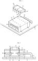
- a protection element 3 such as a variable resistor for preventing static electricity near the connector 1 and a TVS (Transient Voltage Suppressor) diode for preventing transient voltage is disposed on the PCB 2.
- the present disclosure is designed to solve the problems of the related art, and therefore the present disclosure is directed to installing a protection element for preventing ESD or EOS directly to a connector in order to save a component mounting space on a PCB.
- a connector mounted on a printed circuit board comprising: a connector housing; first terminals disposed in an inner space of the connector housing; second terminals configured to extend from the inside of the connector housing to the outside of the connector housing in a state of being separated from the first terminals and be soldered to the PCB; and a protection element configured to electrically connect the first terminals and the second terminals and mounted to one side of the connector housing.
- PCB printed circuit board
- the protection element may have at least one of an ESD prevention function, an EOS prevention function and an EMI prevention function.
- the connector housing may have pin insertion holes formed through an upper plate thereof in an upper and lower direction
- the protection element may include an element body and element pins extending from the center of the element body, the element body may be attached to a surface of the upper plate of the connector housing, and the element pins may come into contact with the first terminals or the second terminals through the pin insertion holes.
- the element pins may include first element pins located at a left side of the element body and second element pins located at a right side of the element body, the first element pins may come into contact with the first terminals in one-to-one relationship, and the second element pins may come into contact with the second terminals in one-to-one relationship.
- the element body may be bonded to the surface of the upper plate of the connector housing.
- the first terminal may include a first vertical part configured to extend vertically from a lower plate of the connector housing; and a first horizontal part configured to extend horizontally from a top end of the first vertical part.
- the first terminal may further include a first groove formed concavely at a spot where the first vertical part intersects with the first horizontal part, and the first element pin may be fitted into the first groove.
- the second terminal may include a second horizontal part configured to extend horizontally on a coaxial line with the first horizontal part; and a second vertical part bent from an end of the second horizontal part and connected to the PCB.
- the second terminal may further include a second groove formed concavely at one side of the second horizontal part, and the second element pin may be fitted into the second groove.
- the protection element may be provided in the connector housing, the first terminal may be connected to one side of the protection element, and the second terminal may be connected to the other side of the protection element.
- the protection element may further include a support member configured to extend downward from a bottom end thereof to be connected to the lower plate of the connector housing or connected onto the PCB through the lower plate of the connector housing.
- a battery pack comprising the connector described above.
- a printed circuit board (PCB) 2 may refer to a BMS circuit board 2 applied to a battery pack for a vehicle.
- the BMS circuit board is a component of the battery pack for controlling charge and discharge of battery cells and cell balancing.
- a connector according to the present disclosure may be used to transmit voltage information of secondary battery cells to a BMS chip.
- the scope of the present disclosure is not limited to this use. That is, the connector according to the present disclosure may also be used to connect various signal transmission cables to electrical tools such as laptops, tablet PCs and smart phones.
- FIG. 2 is a schematic perspective view showing a connector according to an embodiment of the present disclosure
- FIG. 3 is a partially exploded perspective view showing the connector of FIG. 2
- FIG. 4 is a sectional view, taken along the line I-I' of FIG. 2 .
- a connector 100 includes a connector housing 10, first terminals 30 disposed in an inner space of the connector housing 10, second terminals 40 extending from the inside of the connector housing 10 to the outside of the connector housing 10 in a state of being separated from the first terminals 30 and soldered to the PCB 2, and a protection element 20 configured to electrically connect the first terminals 30 and the second terminals 40 and mounted to one side of the connector housing 10.
- the connector 100 may be disposed at an edge region of one side of the PCB 2, and may be connected to and disconnected from a cable connector 200 in a plug-in manner.
- the second terminals 40 of connector 100 are soldered to conductor patterns on the PCB 2, and the conductor patterns may be connected to a BMS chip (ASIC).
- ASIC BMS chip
- the connector housing 10 is a structure to protect the first and second terminals 40 from external shock and to stably connect and fix the cable connector 200, which is a counterpart.
- the connector housing 10 is made of a plastic material with insulating properties, for example, by injection molding.
- the connector housing 10 includes an upper plate 11 provided flat so that the protection element 20 may be placed straight thereon.
- an intaglio is formed at the surface of the upper plate 11 of the connector housing 10 according to the shape of a bottom surface of the protection element 20 so that the protection element 20 is placed in the intaglio portion to reinforce the fixability.
- pin insertion holes 13 may be further provided in the upper plate 11 of the connector housing 10. The pin insertion holes 13 are formed through the upper plate 11 of the connector housing 10 in the upper and lower direction, and element pins of the protection elements 20 may inserted into the connector housing 10 through the pin insertion holes 13.
- the protection element 20 is an electrical component capable of preventing malfunction and damage of other elements around the connector 100, and may have at least one of an ESD prevention function, an EOS prevention function and an EMI prevention function.
- the protection element 20 may employ a variable resistor having an ESD prevention function, a TVS (Transient Voltage Suppressor) diode having an EOS prevention function, or the like.
- the protection element 20 includes an element body 21 and element pins.
- the element body 21 may be implemented in the form of a cuboid-shaped chip, and may be attached to the surface of the upper plate 11 of the connector housing 10.
- the element body 21 is bonded to the surface of the upper plate 11 of the connector housing 10 using an adhesive so that the protection element 20 is not easily separated from the connector housing 10 even by vibration or impact.
- the element pins include first element pins 23 located at a left side of the element body 21 and second element pins 25 located at a right side of the element body 21.
- the first element pins 23 and the second element pins 25 may be provided in the number corresponding to the first terminals 30 and the second terminals 40 employed in the connector housing 10, respectively.
- the terminals are divided into the first terminals 30 and the second terminals 40, unlike the conventional connector 100. That is, the terminals are divided into two parts, namely the first terminals 30 and the second terminals 40, and they are electrically connected only through the protection element 20.
- the element body 21 is placed on the upper plate 11 of the connector housing 10, and the first and second element pins 25 are inserted into the connector housing 10 through the pin insertion holes 13.
- the inserted first element pins 23 are in contact with the first terminals 30 in one-to-one relationship
- the second element pins 25 are in contact with the second terminals 40 in one-to-one relationship.
- the first terminal 30 may correspond to a front end of the existing terminal
- the second terminal 40 may correspond to a rear end of the existing terminal.
- the second terminal 40 may pass through connector housing 10, be bent at the outside, and then be fixed onto the conductor pattern of the PCB 2 by soldering.
- the first terminal 30 is configured to include a first vertical part 31 extending vertically from the lower plate 12 of the connector housing 10 and a first horizontal part 33 extending horizontally from a top end of the first vertical part 31.
- first terminal 30 may further include a first groove 35 formed concavely at a spot where the first vertical part 31 intersects with the first horizontal part 33.
- the first groove 35 may be useful for fitting an end of the first element pin 23.
- the second terminal 40 is configured to include a second horizontal part 43 extending horizontally on a coaxial line with the first horizontal part 33, and a second vertical part 41 bent at one end of the second horizontal part 43 and connected to the PCB 2.
- the second terminal 40 may further include a second groove 45 formed concavely at one side of the second horizontal part 43. Similar to the first groove 35, the second groove 45 may be useful to fit an end of the second element pin 25.
- the first groove 35 is formed at the spot where the first vertical part 31 intersects with the first horizontal part 33, so that the first element pin 23 of the protection element 20 is inserted vertically into the first terminal 30 to prevent that the first terminal 30 from being twisted or inclined.
- the second groove 45 is formed at the second horizontal part 43, and a reinforcing part 44 for supporting the second horizontal part 43 may be further provided below the second groove 45.
- the connector 100 integrated with the protection element 20 according to an embodiment of the present disclosure is used, it is possible to save space for the protection element 20, which has been mounted around the connector 100 in the existing technique, and also to block external electric shock applied from the outside at the connector 100 itself.
- FIG. 5 is a schematic perspective view showing a connector according to another embodiment of the present disclosure.
- the protection element 20 is provided at the outside of the connector housing 10.
- a protection element 20A is provided to be included in the connector housing 10.
- the protection element 20A of the connector 100 has no element pin, and is configured such that the first terminals 30 and the second terminals 40 are directly connected to the protection element 20A.
- the first terminal 30 may be connected to the second terminal 40 via the protection element 20A, the first vertical part 31 may be omitted.
- the structural stability may be secured by providing a support member 27 that extends downward from a bottom end of the protection element 20A and connected to the lower plate 12 of the connector housing 10 or connected onto the PCB 2 through the lower plate 12 of the connector housing 10.
- the support member 27 serves to support the protection element 20A at a certain height inside the connector housing 10.
- the support member 27 may be utilized as a ground line, if necessary.
- a battery pack according to the present disclosure may be configured to include the connector 100 described above.
- the connector 100 may be installed at a BMS circuit board 2 of the battery pack.
- the BMS circuit board 2 is an electrical component of the battery pack to control charging/discharging and cell balancing of battery cells.
- the battery pack may further include a cooling device for managing the temperature of the battery cells, a control device such as a fuse and a relay and for controlling the flow of current, a pack case for packaging the components, or the like.
Landscapes
- Engineering & Computer Science (AREA)
- Microelectronics & Electronic Packaging (AREA)
- Details Of Connecting Devices For Male And Female Coupling (AREA)
- Coupling Device And Connection With Printed Circuit (AREA)
Abstract
Description
- The present disclosure relates to a connector, and more particularly, to a connector having a protection element for protecting a circuit element from ESD or EOS.
- The present application claims priority to
Korean Patent Application No. 10-2019-0113060 filed on September 11, 2019 - A connector is a connection mechanism for constructing an electric circuit by connecting an electric device and a cord or connecting a cord and a cord. Generally, a connector includes a pair of female connector and male connector, which are connected to each other by a receptacle manner. A plurality of female connector pins corresponding to a contact are installed at the female connector, and a plurality of male connector pins making contact with the plurality of female connector pins are installed at the male connector. For example, the male connector may be coupled to a surface of a printed circuit board (PCB) by means of SMT (Surface Mounter Technology), and the female connector may be complementarily fastened with the male connector.
- Meanwhile, the PCB (Printed Circuit Board) includes various chips and components in addition to the connector that mediates the connection with a plurality of boards or other terminals. Recently, as the functions of electronic products have diversified, elements included in the PCB are also becoming more complex.
- As the PCB circuit configuration becomes more complex as above, electrical interference (for example, electromagnetic interference (EMI), electrostatic discharge (ESD)) or electrical over-stress (EOS) is increasing. The electrical interference or electrical over-stress may cause a malfunction of the PCB itself, as well as function deterioration or processing speed reduction of a certain element of the PCB.
- For this reason, in order to protect a specific element (for example, a BMS chip) from ESD or EOS, as shown in
FIG. 1 , aprotection element 3 such as a variable resistor for preventing static electricity near the connector 1 and a TVS (Transient Voltage Suppressor) diode for preventing transient voltage is disposed on thePCB 2. - However, as described above, the circuit configuration of the PCB is becoming more complex, but the appearance of electronic products is becoming more compact, so the space on the PCB where components should be mounted is insufficient. Therefore, it is becoming an issue to secure a mounting area by reducing even one small component.
- The present disclosure is designed to solve the problems of the related art, and therefore the present disclosure is directed to installing a protection element for preventing ESD or EOS directly to a connector in order to save a component mounting space on a PCB.
- In one aspect of the present disclosure, there is provided a connector mounted on a printed circuit board (PCB), comprising: a connector housing; first terminals disposed in an inner space of the connector housing; second terminals configured to extend from the inside of the connector housing to the outside of the connector housing in a state of being separated from the first terminals and be soldered to the PCB; and a protection element configured to electrically connect the first terminals and the second terminals and mounted to one side of the connector housing.
- The protection element may have at least one of an ESD prevention function, an EOS prevention function and an EMI prevention function.
- The connector housing may have pin insertion holes formed through an upper plate thereof in an upper and lower direction, the protection element may include an element body and element pins extending from the center of the element body, the element body may be attached to a surface of the upper plate of the connector housing, and the element pins may come into contact with the first terminals or the second terminals through the pin insertion holes.
- The element pins may include first element pins located at a left side of the element body and second element pins located at a right side of the element body, the first element pins may come into contact with the first terminals in one-to-one relationship, and the second element pins may come into contact with the second terminals in one-to-one relationship.
- The element body may be bonded to the surface of the upper plate of the connector housing.
- The first terminal may include a first vertical part configured to extend vertically from a lower plate of the connector housing; and a first horizontal part configured to extend horizontally from a top end of the first vertical part.
- The first terminal may further include a first groove formed concavely at a spot where the first vertical part intersects with the first horizontal part, and the first element pin may be fitted into the first groove.
- The second terminal may include a second horizontal part configured to extend horizontally on a coaxial line with the first horizontal part; and a second vertical part bent from an end of the second horizontal part and connected to the PCB.
- The second terminal may further include a second groove formed concavely at one side of the second horizontal part, and the second element pin may be fitted into the second groove.
- The protection element may be provided in the connector housing, the first terminal may be connected to one side of the protection element, and the second terminal may be connected to the other side of the protection element.
- The protection element may further include a support member configured to extend downward from a bottom end thereof to be connected to the lower plate of the connector housing or connected onto the PCB through the lower plate of the connector housing.
- In another aspect of the present disclosure, there is also provided a battery pack, comprising the connector described above.
- According to an embodiment of the present disclosure, it is possible to provide a connector integrated with a protection element for preventing ESD or EOS in order to save a component mounting space on a PCB.
- The effect of the present disclosure is not limited to the above-described effects, and effects not mentioned herein will be clearly understood by those skilled in the art from this specification and the accompanying drawings.
-
-
FIG. 1 is a diagram schematically showing a connector and a protection element on a conventional PCB. -
FIG. 2 is a schematic perspective view showing a connector according to an embodiment of the present disclosure. -
FIG. 3 is a partially exploded perspective view showing the connector ofFIG. 2 . -
FIG. 4 is a sectional view, taken along the line I-I' ofFIG. 2 . -
FIG. 5 is a schematic perspective view showing a connector according to another embodiment of the present disclosure. - Hereinafter, preferred embodiments of the present disclosure will be described in detail with reference to the accompanying drawings. Prior to the description, it should be understood that the terms used in the specification and the appended claims should not be construed as limited to general and dictionary meanings, but interpreted based on the meanings and concepts corresponding to technical aspects of the present disclosure on the basis of the principle that the inventor is allowed to define terms appropriately for the best explanation.
- Therefore, the description proposed herein is just a preferable example for the purpose of illustrations only, not intended to limit the scope of the disclosure, so it should be understood that other equivalents and modifications could be made thereto without departing from the scope of the disclosure.
- In the following description, a printed circuit board (PCB) 2 may refer to a
BMS circuit board 2 applied to a battery pack for a vehicle. Here, the BMS circuit board is a component of the battery pack for controlling charge and discharge of battery cells and cell balancing. - A connector according to the present disclosure may be used to transmit voltage information of secondary battery cells to a BMS chip. Here, the scope of the present disclosure is not limited to this use. That is, the connector according to the present disclosure may also be used to connect various signal transmission cables to electrical tools such as laptops, tablet PCs and smart phones.
-
FIG. 2 is a schematic perspective view showing a connector according to an embodiment of the present disclosure,FIG. 3 is a partially exploded perspective view showing the connector ofFIG. 2 , andFIG. 4 is a sectional view, taken along the line I-I' ofFIG. 2 . - Referring to these figures, a
connector 100 according to an embodiment of the present disclosure includes aconnector housing 10,first terminals 30 disposed in an inner space of theconnector housing 10,second terminals 40 extending from the inside of theconnector housing 10 to the outside of theconnector housing 10 in a state of being separated from thefirst terminals 30 and soldered to thePCB 2, and aprotection element 20 configured to electrically connect thefirst terminals 30 and thesecond terminals 40 and mounted to one side of theconnector housing 10. - As shown in
FIG. 2 , theconnector 100 may be disposed at an edge region of one side of thePCB 2, and may be connected to and disconnected from acable connector 200 in a plug-in manner. Although not shown in detail for convenience of drawing, thesecond terminals 40 ofconnector 100 are soldered to conductor patterns on thePCB 2, and the conductor patterns may be connected to a BMS chip (ASIC). - The
connector housing 10 is a structure to protect the first andsecond terminals 40 from external shock and to stably connect and fix thecable connector 200, which is a counterpart. Theconnector housing 10 is made of a plastic material with insulating properties, for example, by injection molding. - The
connector housing 10 includes anupper plate 11 provided flat so that theprotection element 20 may be placed straight thereon. As another example, it is also possible that an intaglio is formed at the surface of theupper plate 11 of theconnector housing 10 according to the shape of a bottom surface of theprotection element 20 so that theprotection element 20 is placed in the intaglio portion to reinforce the fixability. In addition,pin insertion holes 13 may be further provided in theupper plate 11 of theconnector housing 10. Thepin insertion holes 13 are formed through theupper plate 11 of the connector housing 10 in the upper and lower direction, and element pins of theprotection elements 20 may inserted into the connector housing 10 through thepin insertion holes 13. - The
protection element 20 is an electrical component capable of preventing malfunction and damage of other elements around theconnector 100, and may have at least one of an ESD prevention function, an EOS prevention function and an EMI prevention function. For example, theprotection element 20 may employ a variable resistor having an ESD prevention function, a TVS (Transient Voltage Suppressor) diode having an EOS prevention function, or the like. - Referring to
FIGS. 3 and 4 , theprotection element 20 includes anelement body 21 and element pins. - The
element body 21 may be implemented in the form of a cuboid-shaped chip, and may be attached to the surface of theupper plate 11 of theconnector housing 10. Preferably, theelement body 21 is bonded to the surface of theupper plate 11 of theconnector housing 10 using an adhesive so that theprotection element 20 is not easily separated from the connector housing 10 even by vibration or impact. - The element pins include
first element pins 23 located at a left side of theelement body 21 andsecond element pins 25 located at a right side of theelement body 21. Thefirst element pins 23 and thesecond element pins 25 may be provided in the number corresponding to thefirst terminals 30 and thesecond terminals 40 employed in theconnector housing 10, respectively. - In particular, in the
connector 100 according to this embodiment, the terminals are divided into thefirst terminals 30 and thesecond terminals 40, unlike theconventional connector 100. That is, the terminals are divided into two parts, namely thefirst terminals 30 and thesecond terminals 40, and they are electrically connected only through theprotection element 20. - For example, in the
protection element 20, theelement body 21 is placed on theupper plate 11 of theconnector housing 10, and the first and second element pins 25 are inserted into theconnector housing 10 through the pin insertion holes 13. The inserted first element pins 23 are in contact with thefirst terminals 30 in one-to-one relationship, and the second element pins 25 are in contact with thesecond terminals 40 in one-to-one relationship. - Therefore, when the
cable connector 200 serving as a counterpart is plugged into theconnector 100 according to this embodiment, a current flows in the order of thefirst terminal 30, theprotection element 20 and thesecond terminal 40, so it is possible to block an unexpected surge, ESD or EOS at theconnector 100 itself. - Referring to
FIG. 4 again, thefirst terminal 30 according to this embodiment may correspond to a front end of the existing terminal, and thesecond terminal 40 may correspond to a rear end of the existing terminal. Thesecond terminal 40 may pass throughconnector housing 10, be bent at the outside, and then be fixed onto the conductor pattern of thePCB 2 by soldering. - Since the
first terminal 30 is disconnected from thesecond terminal 40, a structure for support thefirst terminal 30 at a certain height is required. To this end, in theconnector 100 of the present disclosure, thefirst terminal 30 is configured to include a firstvertical part 31 extending vertically from thelower plate 12 of theconnector housing 10 and a firsthorizontal part 33 extending horizontally from a top end of the firstvertical part 31. - In addition, the
first terminal 30 may further include afirst groove 35 formed concavely at a spot where the firstvertical part 31 intersects with the firsthorizontal part 33. Thefirst groove 35 may be useful for fitting an end of thefirst element pin 23. - Also, the
second terminal 40 is configured to include a secondhorizontal part 43 extending horizontally on a coaxial line with the firsthorizontal part 33, and a secondvertical part 41 bent at one end of the secondhorizontal part 43 and connected to thePCB 2. - Similar to the
first terminal 30, thesecond terminal 40 may further include asecond groove 45 formed concavely at one side of the secondhorizontal part 43. Similar to thefirst groove 35, thesecond groove 45 may be useful to fit an end of thesecond element pin 25. - The
first groove 35 is formed at the spot where the firstvertical part 31 intersects with the firsthorizontal part 33, so that thefirst element pin 23 of theprotection element 20 is inserted vertically into thefirst terminal 30 to prevent that the first terminal 30 from being twisted or inclined. For the same purpose as thefirst groove 35, thesecond groove 45 is formed at the secondhorizontal part 43, and a reinforcingpart 44 for supporting the secondhorizontal part 43 may be further provided below thesecond groove 45. - If the
connector 100 integrated with theprotection element 20 according to an embodiment of the present disclosure is used, it is possible to save space for theprotection element 20, which has been mounted around theconnector 100 in the existing technique, and also to block external electric shock applied from the outside at theconnector 100 itself. -
FIG. 5 is a schematic perspective view showing a connector according to another embodiment of the present disclosure. - Next, another embodiment of the present disclosure will be briefly described with reference to the
FIG. 5 . The same reference signs as those in the former embodiment denote the same components, and only features different from the former embodiment will be described in detail, without describing the same components again. - In the
connector 100 according to the former embodiment, theprotection element 20 is provided at the outside of theconnector housing 10. However, in theconnector 100 according to this embodiment, aprotection element 20A is provided to be included in theconnector housing 10. - In addition, the
protection element 20A of theconnector 100 according to this embodiment has no element pin, and is configured such that thefirst terminals 30 and thesecond terminals 40 are directly connected to theprotection element 20A. - In this case, since the
first terminal 30 may be connected to thesecond terminal 40 via theprotection element 20A, the firstvertical part 31 may be omitted. Instead, the structural stability may be secured by providing asupport member 27 that extends downward from a bottom end of theprotection element 20A and connected to thelower plate 12 of theconnector housing 10 or connected onto thePCB 2 through thelower plate 12 of theconnector housing 10. Thesupport member 27 serves to support theprotection element 20A at a certain height inside theconnector housing 10. Thesupport member 27 may be utilized as a ground line, if necessary. - In the
connector 100 according to this embodiment as described above, since theprotection element 20A is entirely located inside theconnector housing 10, there is no issue such as breakage of the element pins or removal of theprotection element 20 even though vibration or external impact is applied. - Meanwhile, a battery pack according to the present disclosure may be configured to include the
connector 100 described above. Theconnector 100 may be installed at aBMS circuit board 2 of the battery pack. TheBMS circuit board 2 is an electrical component of the battery pack to control charging/discharging and cell balancing of battery cells. - In addition to the
connector 100, theBMS circuit board 2 and the battery cells, the battery pack may further include a cooling device for managing the temperature of the battery cells, a control device such as a fuse and a relay and for controlling the flow of current, a pack case for packaging the components, or the like. - The present disclosure has been described in detail. However, it should be understood that the detailed description and specific examples, while indicating preferred embodiments of the disclosure, are given by way of illustration only, since various changes and modifications within the scope of the disclosure will become apparent to those skilled in the art from this detailed description.
- Meanwhile, even though the terms expressing directions such as "upper", "lower", "left" and "right" are used in the specification, they are just for convenience of description and can be expressed differently depending on the location of a viewer or a subject, as apparent to those skilled in the art.
Claims (12)
- A connector mounted on a printed circuit board (PCB), comprising:a connector housing;first terminals disposed in an inner space of the connector housing;second terminals configured to extend from the inside of the connector housing to the outside of the connector housing in a state of being separated from the first terminals and be soldered to the PCB; anda protection element configured to electrically connect the first terminals and the second terminals and mounted to one side of the connector housing.
- The connector according to claim 1,
wherein the protection element has at least one of an ESD prevention function, an EOS prevention function and an EMI prevention function. - The connector according to claim 1,wherein the connector housing has pin insertion holes formed through an upper plate thereof in an upper and lower direction,the protection element includes an element body and element pins extending from the element body,the element body is attached to a surface of the upper plate of the connector housing, andthe element pins come into contact with the first terminals or the second terminals through the pin insertion holes.
- The connector according to claim 3,wherein the element pins include first element pins located at a left side of the element body and second element pins located at a right side of the element body, andthe first element pins come into contact with the first terminals in one-to-one relationship and the second element pins come into contact with the second terminals in one-to-one relationship.
- The connector according to claim 3,
wherein the element body is bonded to the surface of the upper plate of the connector housing. - The connector according to claim 4,
wherein the first terminal includes:a first vertical part configured to extend vertically from a lower plate of the connector housing; anda first horizontal part configured to extend horizontally from a top end of the first vertical part. - The connector according to claim 6,wherein the first terminal further includes a first groove formed concavely at a spot where the first vertical part intersects with the first horizontal part, andthe first element pin is fitted into the first groove.
- The connector according to claim 7,
wherein the second terminal includes:a second horizontal part configured to extend horizontally on a coaxial line with the first horizontal part; anda second vertical part bent from an end of the second horizontal part and connected to the PCB. - The connector according to claim 8,wherein the second terminal further includes a second groove formed concavely at one side of the second horizontal part, andthe second element pin is fitted into the second groove.
- The connector according to claim 1,
wherein the protection element is provided in the connector housing, the first terminal is connected to one side of the protection element, and the second terminal is connected to the other side of the protection element. - The connector according to claim 10,
wherein the protection element further includes a support member configured to extend downward from a bottom end thereof to be connected to the lower plate of the connector housing or connected onto the PCB through the lower plate of the connector housing. - A battery pack, comprising the connector according to any one of claims 1 to 11.
Applications Claiming Priority (2)
| Application Number | Priority Date | Filing Date | Title |
|---|---|---|---|
| KR1020190113060A KR102733088B1 (en) | 2019-09-11 | 2019-09-11 | A connector integrated with protection element |
| PCT/KR2020/011332 WO2021049779A1 (en) | 2019-09-11 | 2020-08-25 | Protection element-integrated type connector |
Publications (2)
| Publication Number | Publication Date |
|---|---|
| EP3961824A1 true EP3961824A1 (en) | 2022-03-02 |
| EP3961824A4 EP3961824A4 (en) | 2022-06-08 |
Family
ID=74866726
Family Applications (1)
| Application Number | Title | Priority Date | Filing Date |
|---|---|---|---|
| EP20863646.4A Pending EP3961824A4 (en) | 2019-09-11 | 2020-08-25 | INTEGRATED TYPE CONNECTOR IN A PROTECTION ELEMENT |
Country Status (6)
| Country | Link |
|---|---|
| US (1) | US12040577B2 (en) |
| EP (1) | EP3961824A4 (en) |
| JP (1) | JP7235216B2 (en) |
| KR (1) | KR102733088B1 (en) |
| CN (1) | CN113924699B (en) |
| WO (1) | WO2021049779A1 (en) |
Cited By (1)
| Publication number | Priority date | Publication date | Assignee | Title |
|---|---|---|---|---|
| WO2024020480A1 (en) * | 2022-07-20 | 2024-01-25 | Cps Technology Holdings Llc | Battery management system structure and battery comprising same |
Families Citing this family (5)
| Publication number | Priority date | Publication date | Assignee | Title |
|---|---|---|---|---|
| CN210137029U (en) * | 2019-08-13 | 2020-03-10 | 纽陲客股份公司 | Embedded plug connector |
| KR102330375B1 (en) * | 2021-06-18 | 2021-12-01 | 주식회사 레이닉스 | Connector having protective device |
| KR20230145830A (en) * | 2022-04-11 | 2023-10-18 | 주식회사 엘지에너지솔루션 | Battery pack connector for connecting to external devices |
| CN116191077A (en) * | 2023-03-13 | 2023-05-30 | 北京全路通信信号研究设计院集团有限公司 | track circuit signal transmission device |
| KR20250059806A (en) * | 2023-10-25 | 2025-05-07 | 삼성에스디아이 주식회사 | Protection circuit module and battery pack comprising the same |
Family Cites Families (27)
| Publication number | Priority date | Publication date | Assignee | Title |
|---|---|---|---|---|
| US5256085A (en) | 1992-11-05 | 1993-10-26 | Foxconn International, Inc. | Connector with improved ESD protection mechanism |
| JPH1012776A (en) | 1996-06-19 | 1998-01-16 | Hitachi Ltd | Connection device |
| US5980272A (en) | 1997-10-21 | 1999-11-09 | Hon Hai Precision Ind. Co., Ltd. | Electrical connector with back shell for contact tails |
| JPH11329605A (en) | 1998-05-14 | 1999-11-30 | Mitsumi Electric Co Ltd | Power connector |
| US6522515B1 (en) | 1999-01-08 | 2003-02-18 | Littelfuse, Inc. | Data and power connector port |
| JP3534024B2 (en) | 1999-11-08 | 2004-06-07 | 住友電装株式会社 | Card edge connector |
| KR100445115B1 (en) * | 2002-01-30 | 2004-08-21 | 삼성전자주식회사 | Electronic equipment having a inlet socket for protecting circuit element from surge |
| KR100564898B1 (en) | 2004-03-24 | 2006-03-30 | 텍사스 인스트루먼트 코리아 주식회사 | Overload protection device |
| KR100604076B1 (en) | 2004-07-28 | 2006-07-24 | 주식회사 팬택 | Integrated connector with protective element |
| DE602007004997D1 (en) | 2006-08-16 | 2010-04-08 | Sandisk Corp | CONNECTOR WITH ESD PROTECTION |
| JP4913523B2 (en) | 2006-09-29 | 2012-04-11 | 北陸電気工業株式会社 | Circuit board interconnection connector device |
| TWI358160B (en) | 2007-03-26 | 2012-02-11 | Hon Hai Prec Ind Co Ltd | Electrical card connector |
| JP2008258016A (en) | 2007-04-05 | 2008-10-23 | Smk Corp | Solder connection structure between electronic component terminals and printed wiring board |
| JP2009037913A (en) | 2007-08-02 | 2009-02-19 | Yazaki Corp | Connector and board mounting method of connector |
| CN201230071Y (en) | 2008-06-18 | 2009-04-29 | 富士康(昆山)电脑接插件有限公司 | Electric connector |
| US7878827B2 (en) | 2008-06-06 | 2011-02-01 | Hon Hai Precision Ind. Co., Ltd. | Electrical connector with electrical device incorporated therein |
| CN101740957B (en) | 2008-11-26 | 2012-06-20 | 富士康(昆山)电脑接插件有限公司 | Electric coupler component |
| US9331324B2 (en) | 2009-02-09 | 2016-05-03 | Samsung Sdi Co., Ltd. | Connector assembly and battery pack having the same |
| US8408926B1 (en) * | 2010-12-01 | 2013-04-02 | Nai-Chien Chang | Network connector with switch function |
| KR20120080854A (en) | 2011-01-10 | 2012-07-18 | 삼성모바일디스플레이주식회사 | Flexible printed circuit board connector |
| KR101383444B1 (en) * | 2012-05-18 | 2014-04-08 | 주식회사 후성테크 | Dual electric connector |
| CN102969624A (en) | 2012-11-12 | 2013-03-13 | 华为技术有限公司 | Connector and electronic device |
| JP2016021330A (en) | 2014-07-15 | 2016-02-04 | 株式会社オートネットワーク技術研究所 | Terminal fittings and connectors |
| CN106299927A (en) * | 2015-06-08 | 2017-01-04 | 富士康(昆山)电脑接插件有限公司 | Stack-type electric connector |
| TWM558485U (en) | 2017-12-01 | 2018-04-11 | Cooler Master Tech Inc | Connector structure |
| KR20190113060A (en) | 2018-03-27 | 2019-10-08 | 조선대학교산학협력단 | Wearable bio-signal measuring apparatus |
| CN209045815U (en) | 2018-09-18 | 2019-06-28 | 深圳市泓润电子有限公司 | A kind of connector assembly of battery pack protection board |
-
2019
- 2019-09-11 KR KR1020190113060A patent/KR102733088B1/en active Active
-
2020
- 2020-08-25 JP JP2021537150A patent/JP7235216B2/en active Active
- 2020-08-25 EP EP20863646.4A patent/EP3961824A4/en active Pending
- 2020-08-25 WO PCT/KR2020/011332 patent/WO2021049779A1/en not_active Ceased
- 2020-08-25 US US17/422,271 patent/US12040577B2/en active Active
- 2020-08-25 CN CN202080038292.1A patent/CN113924699B/en active Active
Cited By (1)
| Publication number | Priority date | Publication date | Assignee | Title |
|---|---|---|---|---|
| WO2024020480A1 (en) * | 2022-07-20 | 2024-01-25 | Cps Technology Holdings Llc | Battery management system structure and battery comprising same |
Also Published As
| Publication number | Publication date |
|---|---|
| WO2021049779A1 (en) | 2021-03-18 |
| CN113924699B (en) | 2024-05-10 |
| KR20210031290A (en) | 2021-03-19 |
| US12040577B2 (en) | 2024-07-16 |
| JP2022517063A (en) | 2022-03-04 |
| KR102733088B1 (en) | 2024-11-20 |
| EP3961824A4 (en) | 2022-06-08 |
| JP7235216B2 (en) | 2023-03-08 |
| US20220094109A1 (en) | 2022-03-24 |
| CN113924699A (en) | 2022-01-11 |
Similar Documents
| Publication | Publication Date | Title |
|---|---|---|
| US12040577B2 (en) | Connector integrated with protection element | |
| CN109599690B (en) | Adaptor connector and electric connector assembly | |
| CN103560361B (en) | USB3 adapter | |
| CN204835065U (en) | Connector socket and electronic equipment | |
| KR20200071614A (en) | FPCB assembly for battery module and a method for manufacturing FPCB assembly and a battery module including the same | |
| JP6761730B2 (en) | Electronic devices and connectors | |
| US20120087057A1 (en) | Portable information processing device | |
| EP2876736A1 (en) | Multi connector, wiring method thereof and display apparatus having the same | |
| WO2008083166A2 (en) | Electrical connector with grounding pin | |
| US7625240B2 (en) | Receptacle connector | |
| EP3703197B1 (en) | Connector having surge prevention function and circuit board including same | |
| EP4210180B1 (en) | Connector assembly and manufacturing method therefor, and electronic device | |
| US7189119B2 (en) | Adapter having transient suppression protection | |
| US10811825B2 (en) | Surface mounted HDMI connector | |
| JP2005222855A (en) | Receptacle | |
| KR102204858B1 (en) | Battery Module | |
| CN1349287A (en) | Electric connector | |
| KR101321656B1 (en) | Connector for a high speed memory card adaptor and a socket | |
| KR102732566B1 (en) | Connector having a function as a ground or a ESD protector | |
| US9736955B2 (en) | Circuitry on printed circuit boards in a plurality of planes, having an interface for a plug-in board | |
| US20120122344A1 (en) | Semiconductor-type electric connector | |
| US20250079736A1 (en) | Electric connector and connector assembly | |
| JP2005223201A (en) | Flexible substrate for inter-terminal protection and receptacle including the same | |
| CN211789830U (en) | Electrical connector | |
| CN101436720B (en) | Electronic Card Connector Assembly |
Legal Events
| Date | Code | Title | Description |
|---|---|---|---|
| STAA | Information on the status of an ep patent application or granted ep patent |
Free format text: STATUS: THE INTERNATIONAL PUBLICATION HAS BEEN MADE |
|
| PUAI | Public reference made under article 153(3) epc to a published international application that has entered the european phase |
Free format text: ORIGINAL CODE: 0009012 |
|
| STAA | Information on the status of an ep patent application or granted ep patent |
Free format text: STATUS: REQUEST FOR EXAMINATION WAS MADE |
|
| 17P | Request for examination filed |
Effective date: 20211122 |
|
| AK | Designated contracting states |
Kind code of ref document: A1 Designated state(s): AL AT BE BG CH CY CZ DE DK EE ES FI FR GB GR HR HU IE IS IT LI LT LU LV MC MK MT NL NO PL PT RO RS SE SI SK SM TR |
|
| RAP3 | Party data changed (applicant data changed or rights of an application transferred) |
Owner name: LG ENERGY SOLUTION, LTD. |
|
| REG | Reference to a national code |
Ref country code: DE Ref legal event code: R079 Free format text: PREVIOUS MAIN CLASS: H01R0013659400 Ipc: H01R0012720000 Ref country code: DE Ref legal event code: R079 Ref document number: 602020072417 Country of ref document: DE Free format text: PREVIOUS MAIN CLASS: H01R0013659400 Ipc: H01R0012720000 |
|
| A4 | Supplementary search report drawn up and despatched |
Effective date: 20220509 |
|
| RIC1 | Information provided on ipc code assigned before grant |
Ipc: H05K 3/34 20060101ALN20220502BHEP Ipc: H01R 13/66 20060101ALI20220502BHEP Ipc: H05K 1/02 20060101ALI20220502BHEP Ipc: H01R 13/648 20060101ALI20220502BHEP Ipc: H01R 12/72 20110101AFI20220502BHEP |
|
| DAV | Request for validation of the european patent (deleted) | ||
| DAX | Request for extension of the european patent (deleted) | ||
| STAA | Information on the status of an ep patent application or granted ep patent |
Free format text: STATUS: EXAMINATION IS IN PROGRESS |
|
| 17Q | First examination report despatched |
Effective date: 20240403 |
|
| GRAJ | Information related to disapproval of communication of intention to grant by the applicant or resumption of examination proceedings by the epo deleted |
Free format text: ORIGINAL CODE: EPIDOSDIGR1 |
|
| GRAP | Despatch of communication of intention to grant a patent |
Free format text: ORIGINAL CODE: EPIDOSNIGR1 |
|
| GRAP | Despatch of communication of intention to grant a patent |
Free format text: ORIGINAL CODE: EPIDOSNIGR1 |
|
| STAA | Information on the status of an ep patent application or granted ep patent |
Free format text: STATUS: GRANT OF PATENT IS INTENDED |
|
| RIC1 | Information provided on ipc code assigned before grant |
Ipc: H01R 12/72 20110101AFI20251125BHEP Ipc: H01R 13/648 20060101ALI20251125BHEP Ipc: H05K 1/02 20060101ALI20251125BHEP Ipc: H01R 13/66 20060101ALI20251125BHEP Ipc: H05K 3/34 20060101ALN20251125BHEP |
|
| INTG | Intention to grant announced |
Effective date: 20251211 |
|
| P01 | Opt-out of the competence of the unified patent court (upc) registered |
Free format text: CASE NUMBER: UPC_APP_0000242_3961824/2026 Effective date: 20260106 |
|
| GRAS | Grant fee paid |
Free format text: ORIGINAL CODE: EPIDOSNIGR3 |
|
| GRAA | (expected) grant |
Free format text: ORIGINAL CODE: 0009210 |
|
| STAA | Information on the status of an ep patent application or granted ep patent |
Free format text: STATUS: THE PATENT HAS BEEN GRANTED |