EP3961505A1 - Rfid tag - Google Patents
Rfid tag Download PDFInfo
- Publication number
- EP3961505A1 EP3961505A1 EP20795706.9A EP20795706A EP3961505A1 EP 3961505 A1 EP3961505 A1 EP 3961505A1 EP 20795706 A EP20795706 A EP 20795706A EP 3961505 A1 EP3961505 A1 EP 3961505A1
- Authority
- EP
- European Patent Office
- Prior art keywords
- circuit board
- bound
- rfid
- antenna conductor
- rfid tag
- Prior art date
- Legal status (The legal status is an assumption and is not a legal conclusion. Google has not performed a legal analysis and makes no representation as to the accuracy of the status listed.)
- Withdrawn
Links
Images


Classifications
-
- G—PHYSICS
- G06—COMPUTING OR CALCULATING; COUNTING
- G06K—GRAPHICAL DATA READING; PRESENTATION OF DATA; RECORD CARRIERS; HANDLING RECORD CARRIERS
- G06K19/00—Record carriers for use with machines and with at least a part designed to carry digital markings
- G06K19/06—Record carriers for use with machines and with at least a part designed to carry digital markings characterised by the kind of the digital marking, e.g. shape, nature, code
- G06K19/067—Record carriers with conductive marks, printed circuits or semiconductor circuit elements, e.g. credit or identity cards also with resonating or responding marks without active components
- G06K19/07—Record carriers with conductive marks, printed circuits or semiconductor circuit elements, e.g. credit or identity cards also with resonating or responding marks without active components with integrated circuit chips
- G06K19/077—Constructional details, e.g. mounting of circuits in the carrier
- G06K19/07749—Constructional details, e.g. mounting of circuits in the carrier the record carrier being capable of non-contact communication, e.g. constructional details of the antenna of a non-contact smart card
- G06K19/0775—Constructional details, e.g. mounting of circuits in the carrier the record carrier being capable of non-contact communication, e.g. constructional details of the antenna of a non-contact smart card arrangements for connecting the integrated circuit to the antenna
- G06K19/07754—Constructional details, e.g. mounting of circuits in the carrier the record carrier being capable of non-contact communication, e.g. constructional details of the antenna of a non-contact smart card arrangements for connecting the integrated circuit to the antenna the connection being galvanic
-
- G—PHYSICS
- G06—COMPUTING OR CALCULATING; COUNTING
- G06K—GRAPHICAL DATA READING; PRESENTATION OF DATA; RECORD CARRIERS; HANDLING RECORD CARRIERS
- G06K19/00—Record carriers for use with machines and with at least a part designed to carry digital markings
- G06K19/06—Record carriers for use with machines and with at least a part designed to carry digital markings characterised by the kind of the digital marking, e.g. shape, nature, code
- G06K19/067—Record carriers with conductive marks, printed circuits or semiconductor circuit elements, e.g. credit or identity cards also with resonating or responding marks without active components
- G06K19/07—Record carriers with conductive marks, printed circuits or semiconductor circuit elements, e.g. credit or identity cards also with resonating or responding marks without active components with integrated circuit chips
- G06K19/077—Constructional details, e.g. mounting of circuits in the carrier
- G06K19/07749—Constructional details, e.g. mounting of circuits in the carrier the record carrier being capable of non-contact communication, e.g. constructional details of the antenna of a non-contact smart card
- G06K19/07773—Antenna details
- G06K19/07775—Antenna details the antenna being on-chip
-
- G—PHYSICS
- G06—COMPUTING OR CALCULATING; COUNTING
- G06K—GRAPHICAL DATA READING; PRESENTATION OF DATA; RECORD CARRIERS; HANDLING RECORD CARRIERS
- G06K19/00—Record carriers for use with machines and with at least a part designed to carry digital markings
- G06K19/06—Record carriers for use with machines and with at least a part designed to carry digital markings characterised by the kind of the digital marking, e.g. shape, nature, code
- G06K19/067—Record carriers with conductive marks, printed circuits or semiconductor circuit elements, e.g. credit or identity cards also with resonating or responding marks without active components
- G06K19/07—Record carriers with conductive marks, printed circuits or semiconductor circuit elements, e.g. credit or identity cards also with resonating or responding marks without active components with integrated circuit chips
- G06K19/0701—Record carriers with conductive marks, printed circuits or semiconductor circuit elements, e.g. credit or identity cards also with resonating or responding marks without active components with integrated circuit chips at least one of the integrated circuit chips comprising an arrangement for power management
- G06K19/0707—Record carriers with conductive marks, printed circuits or semiconductor circuit elements, e.g. credit or identity cards also with resonating or responding marks without active components with integrated circuit chips at least one of the integrated circuit chips comprising an arrangement for power management the arrangement being capable of collecting energy from external energy sources, e.g. thermocouples, vibration, electromagnetic radiation
-
- G—PHYSICS
- G06—COMPUTING OR CALCULATING; COUNTING
- G06K—GRAPHICAL DATA READING; PRESENTATION OF DATA; RECORD CARRIERS; HANDLING RECORD CARRIERS
- G06K19/00—Record carriers for use with machines and with at least a part designed to carry digital markings
- G06K19/06—Record carriers for use with machines and with at least a part designed to carry digital markings characterised by the kind of the digital marking, e.g. shape, nature, code
- G06K19/067—Record carriers with conductive marks, printed circuits or semiconductor circuit elements, e.g. credit or identity cards also with resonating or responding marks without active components
- G06K19/07—Record carriers with conductive marks, printed circuits or semiconductor circuit elements, e.g. credit or identity cards also with resonating or responding marks without active components with integrated circuit chips
- G06K19/0701—Record carriers with conductive marks, printed circuits or semiconductor circuit elements, e.g. credit or identity cards also with resonating or responding marks without active components with integrated circuit chips at least one of the integrated circuit chips comprising an arrangement for power management
- G06K19/0715—Record carriers with conductive marks, printed circuits or semiconductor circuit elements, e.g. credit or identity cards also with resonating or responding marks without active components with integrated circuit chips at least one of the integrated circuit chips comprising an arrangement for power management the arrangement including means to regulate power transfer to the integrated circuit
-
- G—PHYSICS
- G06—COMPUTING OR CALCULATING; COUNTING
- G06K—GRAPHICAL DATA READING; PRESENTATION OF DATA; RECORD CARRIERS; HANDLING RECORD CARRIERS
- G06K19/00—Record carriers for use with machines and with at least a part designed to carry digital markings
- G06K19/06—Record carriers for use with machines and with at least a part designed to carry digital markings characterised by the kind of the digital marking, e.g. shape, nature, code
- G06K19/067—Record carriers with conductive marks, printed circuits or semiconductor circuit elements, e.g. credit or identity cards also with resonating or responding marks without active components
- G06K19/07—Record carriers with conductive marks, printed circuits or semiconductor circuit elements, e.g. credit or identity cards also with resonating or responding marks without active components with integrated circuit chips
- G06K19/072—Record carriers with conductive marks, printed circuits or semiconductor circuit elements, e.g. credit or identity cards also with resonating or responding marks without active components with integrated circuit chips the record carrier comprising a plurality of integrated circuit chips
-
- H—ELECTRICITY
- H01—ELECTRIC ELEMENTS
- H01Q—ANTENNAS, i.e. RADIO AERIALS
- H01Q1/00—Details of, or arrangements associated with, antennas
- H01Q1/12—Supports; Mounting means
- H01Q1/22—Supports; Mounting means by structural association with other equipment or articles
- H01Q1/2208—Supports; Mounting means by structural association with other equipment or articles associated with components used in interrogation type services, i.e. in systems for information exchange between an interrogator/reader and a tag/transponder, e.g. in Radio Frequency Identification [RFID] systems
-
- H—ELECTRICITY
- H05—ELECTRIC TECHNIQUES NOT OTHERWISE PROVIDED FOR
- H05K—PRINTED CIRCUITS; CASINGS OR CONSTRUCTIONAL DETAILS OF ELECTRIC APPARATUS; MANUFACTURE OF ASSEMBLAGES OF ELECTRICAL COMPONENTS
- H05K1/00—Printed circuits
- H05K1/02—Details
- H05K1/0213—Electrical arrangements not otherwise provided for
- H05K1/0237—High frequency adaptations
- H05K1/0243—Printed circuits associated with mounted high frequency components
-
- H—ELECTRICITY
- H05—ELECTRIC TECHNIQUES NOT OTHERWISE PROVIDED FOR
- H05K—PRINTED CIRCUITS; CASINGS OR CONSTRUCTIONAL DETAILS OF ELECTRIC APPARATUS; MANUFACTURE OF ASSEMBLAGES OF ELECTRICAL COMPONENTS
- H05K2201/00—Indexing scheme relating to printed circuits covered by H05K1/00
- H05K2201/10—Details of components or other objects attached to or integrated in a printed circuit board
- H05K2201/10007—Types of components
- H05K2201/10098—Components for radio transmission, e.g. radio frequency identification [RFID] tag, printed or non-printed antennas
Definitions
- the present disclosure relates to an RFID (Radio Frequency Identifier) tag having a functional module(s).
- RFID Radio Frequency Identifier
- JP 2002-65418 A RFID tag having functional modules, such as a solar cell and a liquid crystal display device.
- An RFID tag according to the present invention includes:
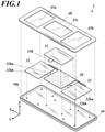
- FIG. 1 is an exploded perspective view of an RFID tag according to an embodiment of the present disclosure.
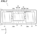
- FIG. 2 is a plan view of configuration in which a circuit board and functional modules are mounted in a case.
- FIG. 3 is a vertical sectional view of the RFID tag of the embodiment.
- a display 33 is indicated by a long dashed double-short dashed line.
- FIG. 3 shows a section at the position of an arrowed A-A line in FIG. 2 .
- directions are described using directions of three axes, X, Y and Z, shown in the drawings.
- the X axis, Y axis and Z axis are three axes that are at right angles to one another.
- the X direction, Y direction and Z direction may be referred to as right-left/lateral direction, up-down direction and front-back direction, respectively.
- the directions described in this description are the same as directions of an RFID tag 1 in use.
- an RFID tag 1 of an embodiment includes a case 10, a circuit board 20, photovoltaic panels 31, 32 as functional modules, a display 33 and a lid 40.
- the case 10 is concave with one side opened, and can accommodate the circuit board 20 and the display 33 on top of one another and the two photovoltaic panels 31, 32 on the left and right of the display 33.
- the case 10 is made of, as a main material, engineering plastic, such as ABS (acrylonitrile butadiene styrene resin), PC (polycarbonate), POM (polyacetal), PP (polypropylene), PPS (polyphenylene sulfite), PA (polyamide), EVA (ethylene vinyl acetate copolymer), PE (polyethylene), PBT (polybutylene terephthalate), PS (polystyrene), EP (epoxy resin) or PF (phenolic resin), and formed, for example, by injection molding.
- the case 10 may be formed of a mixture of any of the above materials as a main material with another material, or may be formed of such a material further containing inorganic filler.
- the circuit board 20 has a main part 20A extending in the X, Y directions and an extended part 20B extending along the upper side (edge) of the main part 20A and extending long on both sides of the main part 20A in the X direction.
- an imaginary border line E1 between the main part 20A and the extended part 20B is shown.
- the main part 20A may be rectangular in plan view.
- the extended part 20B includes an antenna conductor 28 and is integrated with the main part 20A.
- the antenna conductor 28 is formed on a surface (e.g. rear surface in FIG. 1 and FIG. 2 ) of the circuit board 20.
- An electromagnetic field that is radiated from the antenna conductor 28 is radiated in all directions in the YZ plane perpendicular to the longer direction of the antenna conductor 28 (X direction).
- the antenna conductor 28 may be formed on an interlayer of the circuit board 20.
- the antenna conductor 28 includes a linear part 28a for radio wave radiation that resonates at the frequency of a radio signal and a pattern part 28b for impedance matching.
- the linear part 28a extends in the X direction to areas where the photovoltaic panels 31, 32 are arranged.
- the linear part 28a is longer than the lateral width of the main part 20A, and extends longer than the main part 20A in one direction and the other direction of the X direction.
- the linear part 28a may constitute a dipole antenna having an electrical length that is a length of about a half wavelength of a radio signal of an RFID IC 25.
- the pattern part 28b has, for example, a loop-shaped pattern, and is disposed between the linear part 28a and a feeding point for the RFID IC 25 and matches impedances of these.
- the display 33 is, for example, a liquid crystal display panel, and electrically connected to the circuit board 20 through a wiring (e.g. a film wiring) 33h. As shown in FIG. 2 , the display 33 overlaps the main part 20A of the circuit board 20 in the Z direction and does not overlap the extended part 20B thereof in the Z direction. The display 33 may overlap the pattern part 28b and the extended part 20B as long as it does not overlap the linear part 28a of the antenna conductor 28.
- a wiring e.g. a film wiring
- the photovoltaic panels 31, 32 generate electric power by receiving light from outside.
- Each of the photovoltaic panels 31, 32 may have a shape of a rectangular plate.
- the photovoltaic panels 31, 32 are electrically connected to the circuit board 20 through lead wires 31ha, 31hb, 32ha, 32hb that are coated wirings.
- the photovoltaic panels 31, 32 are arranged, of the circuit board 20, in both armpit parts two sides of each of which are delimited by the main part 20A and the extended part 20B of the circuit board 20.
- the photovoltaic panels 31, 32 may be arranged so as to overlap the display 33 and not to overlap the circuit board 20.
- the lead wires 31ha, 31hb, 32ha, 32hb for the photovoltaic panels 31, 32 may be arranged so as to be covered by the photovoltaic panels 31, 32 in the Z direction except for some parts, and may be arranged at a height where they overlap the circuit board 20 as viewed in the direction along the XY plane.
- the lid 40 has transparent windows 41a to 41c in areas respectively facing the photovoltaic panels 31, 32 and the display 33, and is joined to the inner frame 10a of the case 10 to seal off the case 10.
- FIG. 4 is a block diagram showing circuit configuration of the RFID tag of the embodiment.
- the RFID tag 1 includes a PMIC (Power Management Integrated Circuit) 21 that receives generated power from the photovoltaic panels 31, 32 and manages the power, a first power supply IC 22 that receives power from the PMIC 21 and generates a power supply voltage for a control system, and a second power supply IC 23 that receives power from the PMIC 21 and generates a drive voltage for the display 33.
- the RFID tag 1 also includes the RFID IC 25 that performs wireless communication with a reader/writer through radio waves and a control circuit 24 that communicates with the RFID IC 25 and controls display of the display 33. The control circuit 24 and the RFID IC 25 operate by receiving the power supply voltage from the first power supply IC 22.
- the RFID IC 25 performs wireless communication by using, for example, radio waves in the UHF (Ultra High Frequency) band.
- the RFID IC 25 includes a reader/writer readable/writable storage. In the storage, identification information, management information and/or the like is stored.
- the control circuit 24 is, for example, a microcomputer, and can read out the information in the storage of the RFID IC 25 by communicating with the RFID IC 25.
- the control circuit 24 controls display content of the display 33 on the basis of the read-out information.
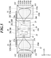
- FIG. 5 is a back view of the circuit board and the functional modules.
- the PMIC 21, the first power supply IC 22, the second power supply IC 23, the control circuit 24, the RFID IC 25 and so forth are mounted on the main part 20A of the circuit board 20, the PMIC 21, the first power supply IC 22, the second power supply IC 23, the control circuit 24, the RFID IC 25 and so forth are mounted. Further, on the circuit board 20, a connector 29 to which the wiring 33h for the display 33 is detachably connected and connectors 26a, 26b, 27a, 27b to which the lead wires 31ha, 31hb, 32ha, 32hb are detachably connected respectively are mounted.
- the photovoltaic panel 31 has, on its outer surface, two outer electrodes 311, 312 to which generated power is output.
- power generation cells each configured such that a semiconductor is interposed between inner electrodes are arranged, and these power generation cells are connected in series.
- back-surface-side inner electrodes 315a to 315h are indicated by broken lines.
- the outer electrode 311 is connected to the inner electrode 315h of the power generation cell disposed at one end of this series connection, and the outer electrode 312 is connected to the inner electrode 315a of the power generation cell disposed at the other end.
- the outer electrode 311 and the inner electrode 315h at one end are electrically connected, without high impedance.
- the inner electrode 315h is connected to the other inner electrodes 315a to 315g and front-surface-side inner electrodes (transparent electrodes) through high impedance semiconductors or the like.
- the outer electrode 312 and the inner electrode 315a at the other end are electrically connected, without high impedance.
- the inner electrode 315a is connected to the other inner electrodes 315b to 315h and the front-surface-side inner electrodes (transparent electrodes) through the high impedance semiconductors or the like.
- These two outer electrodes 311, 312 may be arranged at two corners of the photovoltaic panel 31 in plan view (two corners that are far from the main part 20A of the circuit board 20 in the X direction and also one corner and the other corner in the Y direction).
- the outer electrode 311 is connected to an element (e.g. an input terminal of the PMIC 21) on the circuit board 20 through the lead wire 31ha and a board wiring 201 on the circuit board 20. That is, the photovoltaic panel 31 and the element on the circuit board 20 are electrically connected through a connection wiring 51 into which the lead wire 31ha, a wiring conductor in the connector 26a, the board wiring 201 and the inner electrode 315h are combined.
- the wiring conductor in the connector 26a refers to a path part having the minimum resistance through which current flows from the lead wire 31ha to the board wiring 201.
- One end and the other end of the connection wiring 51 are connected to high impedance terminals, and the part between these two ends is a transmission path for low impedance power (or signal).
- the high impedance terminals each mean, for example, a terminal having a higher impedance than that of a connection part of the connector 26a.
- the impedance means a value at the radio frequency of an RFID.
- a high impedance element such as a diode
- the connection wiring 51 corresponds to a wiring of a section from an end of the inner electrode 315h of the photovoltaic panel 31 to the diode.
- a capacitor is disposed, for example, in front of the input terminal of the PMIC 21, the connection wiring 51 corresponds to a wiring of a section from an end of the inner electrode 315h of the photovoltaic panel 31 to the capacitor.
- connection wiring 51 (inner electrode 315h, lead wire 31ha, wiring conductor in connector 26a and board wiring 201) is within ⁇ 10% of a half wavelength of a radio signal that the RFID IC 25 transmits or receives.
- the electrical length of the connection wiring 51 may be within ⁇ 5% of the half wavelength of the radio signal.
- the electrical length of the connection wiring 51 may be within ⁇ 10% or ⁇ 5% of an integral multiple of the half wavelength of the radio signal.
- the "within ⁇ N% of M” means "(M - M ⁇ N%) to (M + M ⁇ N%)".
- the outer electrode 312 is connected to an element (e.g. a ground terminal of the PMIC 21) on the circuit board 20 through the lead wire 31hb and a ground electrode of the circuit board 20.
- the ground electrode may extend on most of the main part 20A of the circuit board 20.
- the outer electrode 312 is electrically connected to the inner electrode 315a of the photovoltaic panel 31.
- the lead wire 31hb may have approximately the same length as the lead wire 31ha.
- the electrical length of a wiring into which the lead wire 31hb, the inner electrode 315a, a wiring conductor in the connector 26b and the ground electrode are combined may be the same as the electrical length of the connection wiring 51 described above.
- the length of the wiring conductor and the ground electrode refers to a path part having the minimum resistance through which current flows from the lead wire 31hb to the ground terminal of the PMIC 21.
- the two lead wires 31ha, 31hb connected to the photovoltaic panel 31 are partly bound with tape or the like.
- the bound part is referred to as a bound part 31hx.
- the two lead wires 31ha, 31hb intersect at the bound part 31hx, but may not intersect.
- the bound part 31hx may be fixed to the back surface of the photovoltaic panel 31.
- the bound form of lead wires is not limited to the form in which lead wires are bound with a single binding tool (e.g. tape), but includes the form in which lead wires are individually fixed to something other than the lead wires, thereby being kept in a state in which parts thereof are close to one another. In this case, the point where parts of lead wires are close to one another corresponds to the bound part.
- the bound part 31hx is arranged on the opposite side of the center of the photovoltaic panel 31 from the main part 20A of the circuit board 20 (which may be referred to as the opposite side of the center of the photovoltaic panel 31 from the connectors 26a, 26b, or, of the center of the photovoltaic panel 31, the side where the outer electrodes 311, 312 are present). Further, the bound part 31hx is positioned, in the X direction, outward from an end of the antenna conductor 28 (which may be referred to as the opposite side of an end of the antenna conductor 28 from the central part of the antenna conductor 28). That is, the bound part 31hx is arranged so as not to overlap the antenna conductor 28 as viewed in the Y direction.
- the photovoltaic panel 32 has two outer electrodes 321, 322 to which generated power is output and power generation cells including back-surface-side inner electrodes 325a to 325h, and is connected to the connectors 27a, 27b on the circuit board 20 through the two lead wires 32ha, 32hb.
- the connection configuration of these is approximately the same as that regarding the photovoltaic panel 31 except that they are symmetrical.
- the electrical length of a connection wiring 52 (inner electrode 325h, lead wire 32ha, wiring conductor in connector 27a and board wiring 202) for the photovoltaic panel 32 is the same as the electrical length of the connection wiring 51.
- the two lead wires 32ha, 32hb connected to the photovoltaic panel 32 are partly bound with tape or the like to form a bound part 32hx.
- the two lead wires 32ha, 32hb may or may not intersect at the bound part 32hx.
- the bound part 32hx is the same as the bound part 31hx except that they are symmetrical in fixation and arrangement.
- FIG. 6 is a graph showing a relationship between a wiring length and a communicable distance.
- connection wirings 51, 52 having a length that was different from device to device, so that results shown in FIG. 6 were obtained.
- the electrical length of the connection wirings 51, 52 of the testing devices a plurality of lengths was employed, which ranged from 153 mm to 173 mm including, at the center, 163 mm, which is the half wavelength in vacuum for 920 MHz, which is the frequency of the radio signal.
- the results of the communication test are as follows: regarding the testing device having 163 mm as the electrical length, the communicable distance was long and the variance value thereof was small, and regarding each of the testing devices respectively having 153 mm and 173 mm as the electrical length, the average value of the communicable distance was low and the variance value thereof was large.
- FIG. 7 is a graph showing a relationship between a bound position of lead wires and the communicable distance.
- the communication test was conducted on a plurality of testing devices employing a bound part 31hx of lead wires 31ha, 31hb for a photovoltaic panel 31 and a bound part 32hx of lead wires 32ha, 32hb for a photovoltaic panel 32, wherein the positions of the bound parts 31hx, 32hx were changed in the X direction and the Y direction from device to device, so that results shown in FIG. 7 were obtained.
- the results of the communication test are as follows: regarding the case where the bound parts 31hx, 32hx were each positioned 15 mm from the end in the X direction, the average value of the communicable distance was high and the variance thereof was small, regarding the case where the bound parts 31hx, 32hx were each positioned 5 mm from the end, the average value of the communicable distance was high but the variance thereof was large, and regarding the case where the bound parts 31hx, 32hx were each positioned 25 mm from the end, the average value of the communicable distance decreased and the variance thereof was large.
- the "15 mm from the end” corresponds to a position that is on the opposite side of the center of the photovoltaic panel 31/32 from the main part 20A of the circuit board 20 and where the bound part 31hx/32hx does not overlap (the linear part 28a of) the antenna conductor 28 as viewed in the Y direction.
- the "25 mm from the end” corresponds to a position that is in the vicinity of the center of the photovoltaic panel 31/32 and where the bound part 31hx/32hx overlaps (the linear part 28a of) the antenna conductor 28 at an end of the antenna conductor 28 as viewed in the Y direction.
- the positions of the bound parts 31hx, 32hx in the Y direction in the range of -10 mm to +10 mm, no significant difference was observed in either the average value or the variance of the communicable distance.
- the electrical length of the connection wirings 51, 52 can be adjusted to the half wavelength of the radio signal even if the lead wires 31ha, 32ha are short.
- the outer electrodes 311, 312, 321, 322 of the photovoltaic panels 31, 32 may each be arranged on a side close to the main part 20A of the circuit board 20.
- the bound part 31hx may be arranged as described above, and similarly, if the two lead wires 32ha, 32hb are bound, the bound part 32hx may be arranged as described above.
- the two lead wires 31ha, 31hb may or may not intersect at the bound part 31hx, and similarly, the two lead wires 32ha, 32hb may or may not intersect at the bound part 32hx.
- the electrical length of the connection wiring 51 from a point in the photovoltaic panel 31 to an element (PMIC 21) on the circuit board 20 is within ⁇ 10% of the half wavelength of the radio signal.
- This configuration can reduce an effect of the connection wiring 51 absorbing radio waves, which are radiated from the antenna conductor 28, and consequently can lengthen the communicable distance.
- the bound part 31hx of the lead wires 31ha, 31hb is disposed on the opposite side of the center of the photovoltaic panel 32 from the connectors 26a, 26b.
- the two lead wires 31ha, 31hb are present close to one another at the bound part 31hx, where the effect of absorbing radio waves is higher than the other parts.
- strong electric fields are generated at the both ends of the linear part 28a and near the feeding point to which the RFID IC 25 is connected.
- the above arrangement of the bound part 31hx can make itself away from, of the antenna conductor 28, the feeding point where a strong electric field is generated.
- the bound part 31hx of the lead wires 31ha, 31hb is disposed outward from an end of the antenna conductor 28 (i.e. on the opposite side of an end of the antenna conductor 28 from the center of the antenna conductor 28).
- This arrangement can make the bound part 31hx away from, of the antenna conductor 28, an end where a strong electric field is generated. This can reduce the effect of the lead wires 31ha, 31hb absorbing radio waves, which are radiated from the antenna conductor 28, and consequently can lengthen the communicable distance.
- the two photovoltaic panels 31, 32 are used as the functional modules, but, as the functional modules, various modules may be used. Examples thereof include: sensor modules that detect temperature, humidity, illuminance, oscillation, acceleration and so forth; sound collectors; and loudspeakers.
- the display in the embodiment may be used as a functional module, and the electrical length of a wiring thereof may be made to correspond to the half wavelength of the radio signal.
- the details described in the embodiment can be appropriately modified within a range not departing from the scope of the invention.
- the present disclosure is applicable to an RFID (Radio Frequency Identifier) tag having a functional module(s).
- RFID Radio Frequency Identifier
Landscapes
- Engineering & Computer Science (AREA)
- Microelectronics & Electronic Packaging (AREA)
- Computer Hardware Design (AREA)
- Physics & Mathematics (AREA)
- General Physics & Mathematics (AREA)
- Theoretical Computer Science (AREA)
- Computer Networks & Wireless Communication (AREA)
- Electromagnetism (AREA)
- Details Of Aerials (AREA)
- Photovoltaic Devices (AREA)
Abstract
Description
- The present disclosure relates to an RFID (Radio Frequency Identifier) tag having a functional module(s).
- There is disclosed in
JP 2002-65418 A - An RFID tag according to the present invention includes:
- a circuit board having an antenna conductor;
- an RFID IC mounted on the circuit board; and
- a functional module connected to the circuit board through a lead wire,
- wherein an electrical length of a connection wiring that electrically connects the functional module to an element on the circuit board is within ±10% of an integral multiple of a half wavelength of a radio signal that the RFID IC transmits or receives.
-
-
FIG. 1 is an exploded perspective view of an RFID tag according to an embodiment of the present disclosure. -
FIG. 2 is a plan view of configuration in which a circuit board and functional modules are mounted in a case. -
FIG. 3 is a vertical sectional view of the RFID tag of the embodiment. -
FIG. 4 is a block diagram showing circuit configuration of the RFID tag of the embodiment. -
FIG. 5 is a back view of the circuit board and the functional modules. -
FIG. 6 is a graph showing a relationship between a wiring length and a communicable distance. -
FIG. 7 is a graph showing a relationship between a bound position of lead wires and the communicable distance. - Hereinafter, an embodiment of the present disclosure will be described in detail with reference to the drawings.
-
FIG. 1 is an exploded perspective view of an RFID tag according to an embodiment of the present disclosure.FIG. 2 is a plan view of configuration in which a circuit board and functional modules are mounted in a case.FIG. 3 is a vertical sectional view of the RFID tag of the embodiment. InFIG. 2 andFIG. 3 , adisplay 33 is indicated by a long dashed double-short dashed line.FIG. 3 shows a section at the position of an arrowed A-A line inFIG. 2 . In this description, directions are described using directions of three axes, X, Y and Z, shown in the drawings. The X axis, Y axis and Z axis are three axes that are at right angles to one another. The X direction, Y direction and Z direction may be referred to as right-left/lateral direction, up-down direction and front-back direction, respectively. However, it is unnecessary that the directions described in this description are the same as directions of an RFID tag 1 in use. - As shown in
FIG. 1 , an RFID tag 1 of an embodiment includes acase 10, acircuit board 20,photovoltaic panels display 33 and alid 40. - The
case 10 is concave with one side opened, and can accommodate thecircuit board 20 and thedisplay 33 on top of one another and the twophotovoltaic panels display 33. Thecase 10 is made of, as a main material, engineering plastic, such as ABS (acrylonitrile butadiene styrene resin), PC (polycarbonate), POM (polyacetal), PP (polypropylene), PPS (polyphenylene sulfite), PA (polyamide), EVA (ethylene vinyl acetate copolymer), PE (polyethylene), PBT (polybutylene terephthalate), PS (polystyrene), EP (epoxy resin) or PF (phenolic resin), and formed, for example, by injection molding. Thecase 10 may be formed of a mixture of any of the above materials as a main material with another material, or may be formed of such a material further containing inorganic filler. - The
circuit board 20 has amain part 20A extending in the X, Y directions and anextended part 20B extending along the upper side (edge) of themain part 20A and extending long on both sides of themain part 20A in the X direction. InFIG. 2 , an imaginary border line E1 between themain part 20A and theextended part 20B is shown. Themain part 20A may be rectangular in plan view. - The
extended part 20B includes anantenna conductor 28 and is integrated with themain part 20A. Theantenna conductor 28 is formed on a surface (e.g. rear surface inFIG. 1 andFIG. 2 ) of thecircuit board 20. An electromagnetic field that is radiated from theantenna conductor 28 is radiated in all directions in the YZ plane perpendicular to the longer direction of the antenna conductor 28 (X direction). Theantenna conductor 28 may be formed on an interlayer of thecircuit board 20. - The
antenna conductor 28 includes alinear part 28a for radio wave radiation that resonates at the frequency of a radio signal and apattern part 28b for impedance matching. Thelinear part 28a extends in the X direction to areas where thephotovoltaic panels linear part 28a is longer than the lateral width of themain part 20A, and extends longer than themain part 20A in one direction and the other direction of the X direction. Thelinear part 28a may constitute a dipole antenna having an electrical length that is a length of about a half wavelength of a radio signal of anRFID IC 25. Thepattern part 28b has, for example, a loop-shaped pattern, and is disposed between thelinear part 28a and a feeding point for theRFID IC 25 and matches impedances of these. - The
display 33 is, for example, a liquid crystal display panel, and electrically connected to thecircuit board 20 through a wiring (e.g. a film wiring) 33h. As shown inFIG. 2 , thedisplay 33 overlaps themain part 20A of thecircuit board 20 in the Z direction and does not overlap theextended part 20B thereof in the Z direction. Thedisplay 33 may overlap thepattern part 28b and theextended part 20B as long as it does not overlap thelinear part 28a of theantenna conductor 28. - The
photovoltaic panels photovoltaic panels photovoltaic panels circuit board 20 through lead wires 31ha, 31hb, 32ha, 32hb that are coated wirings. As shown inFIG. 2 , thephotovoltaic panels circuit board 20, in both armpit parts two sides of each of which are delimited by themain part 20A and theextended part 20B of thecircuit board 20. As shown inFIG. 3 , as viewed in a direction along the XY plane, thephotovoltaic panels display 33 and not to overlap thecircuit board 20. The lead wires 31ha, 31hb, 32ha, 32hb for thephotovoltaic panels photovoltaic panels circuit board 20 as viewed in the direction along the XY plane. - The
lid 40 hastransparent windows 41a to 41c in areas respectively facing thephotovoltaic panels display 33, and is joined to theinner frame 10a of thecase 10 to seal off thecase 10. -
FIG. 4 is a block diagram showing circuit configuration of the RFID tag of the embodiment. - The RFID tag 1 includes a PMIC (Power Management Integrated Circuit) 21 that receives generated power from the
photovoltaic panels power supply IC 22 that receives power from thePMIC 21 and generates a power supply voltage for a control system, and a secondpower supply IC 23 that receives power from thePMIC 21 and generates a drive voltage for thedisplay 33. The RFID tag 1 also includes theRFID IC 25 that performs wireless communication with a reader/writer through radio waves and acontrol circuit 24 that communicates with theRFID IC 25 and controls display of thedisplay 33. Thecontrol circuit 24 and the RFID IC 25 operate by receiving the power supply voltage from the firstpower supply IC 22. The RFID IC 25 performs wireless communication by using, for example, radio waves in the UHF (Ultra High Frequency) band. The RFID IC 25 includes a reader/writer readable/writable storage. In the storage, identification information, management information and/or the like is stored. Thecontrol circuit 24 is, for example, a microcomputer, and can read out the information in the storage of theRFID IC 25 by communicating with theRFID IC 25. Thecontrol circuit 24 controls display content of thedisplay 33 on the basis of the read-out information. -
FIG. 5 is a back view of the circuit board and the functional modules. - As shown in
FIG. 5 , on themain part 20A of thecircuit board 20, thePMIC 21, the firstpower supply IC 22, the secondpower supply IC 23, thecontrol circuit 24, theRFID IC 25 and so forth are mounted. Further, on thecircuit board 20, aconnector 29 to which thewiring 33h for thedisplay 33 is detachably connected andconnectors - The
photovoltaic panel 31 has, on its outer surface, twoouter electrodes photovoltaic panel 31, power generation cells each configured such that a semiconductor is interposed between inner electrodes are arranged, and these power generation cells are connected in series. InFIG. 5 , back-surface-sideinner electrodes 315a to 315h are indicated by broken lines. Theouter electrode 311 is connected to theinner electrode 315h of the power generation cell disposed at one end of this series connection, and theouter electrode 312 is connected to theinner electrode 315a of the power generation cell disposed at the other end. Theouter electrode 311 and theinner electrode 315h at one end are electrically connected, without high impedance. Theinner electrode 315h is connected to the otherinner electrodes 315a to 315g and front-surface-side inner electrodes (transparent electrodes) through high impedance semiconductors or the like. Theouter electrode 312 and theinner electrode 315a at the other end are electrically connected, without high impedance. Theinner electrode 315a is connected to the otherinner electrodes 315b to 315h and the front-surface-side inner electrodes (transparent electrodes) through the high impedance semiconductors or the like. These twoouter electrodes photovoltaic panel 31 in plan view (two corners that are far from themain part 20A of thecircuit board 20 in the X direction and also one corner and the other corner in the Y direction). - The
outer electrode 311 is connected to an element (e.g. an input terminal of the PMIC 21) on thecircuit board 20 through the lead wire 31ha and aboard wiring 201 on thecircuit board 20. That is, thephotovoltaic panel 31 and the element on thecircuit board 20 are electrically connected through aconnection wiring 51 into which the lead wire 31ha, a wiring conductor in theconnector 26a, theboard wiring 201 and theinner electrode 315h are combined. The wiring conductor in theconnector 26a refers to a path part having the minimum resistance through which current flows from the lead wire 31ha to theboard wiring 201. One end and the other end of theconnection wiring 51 are connected to high impedance terminals, and the part between these two ends is a transmission path for low impedance power (or signal). The high impedance terminals each mean, for example, a terminal having a higher impedance than that of a connection part of theconnector 26a. Herein, the impedance means a value at the radio frequency of an RFID. If a high impedance element, such as a diode, is disposed, for example, in front of the input terminal of thePMIC 21, theconnection wiring 51 corresponds to a wiring of a section from an end of theinner electrode 315h of thephotovoltaic panel 31 to the diode. If a capacitor is disposed, for example, in front of the input terminal of thePMIC 21, theconnection wiring 51 corresponds to a wiring of a section from an end of theinner electrode 315h of thephotovoltaic panel 31 to the capacitor. - The electrical length of the connection wiring 51 (
inner electrode 315h, lead wire 31ha, wiring conductor inconnector 26a and board wiring 201) is within ±10% of a half wavelength of a radio signal that theRFID IC 25 transmits or receives. The electrical length of theconnection wiring 51 may be within ±5% of the half wavelength of the radio signal. The electrical length of theconnection wiring 51 may be within ±10% or ±5% of an integral multiple of the half wavelength of the radio signal. The "within ±N% of M" means "(M - M × N%) to (M + M × N%)". - The
outer electrode 312 is connected to an element (e.g. a ground terminal of the PMIC 21) on thecircuit board 20 through the lead wire 31hb and a ground electrode of thecircuit board 20. The ground electrode may extend on most of themain part 20A of thecircuit board 20. Theouter electrode 312 is electrically connected to theinner electrode 315a of thephotovoltaic panel 31. The lead wire 31hb may have approximately the same length as the lead wire 31ha. The electrical length of a wiring into which the lead wire 31hb, theinner electrode 315a, a wiring conductor in theconnector 26b and the ground electrode are combined may be the same as the electrical length of theconnection wiring 51 described above. The length of the wiring conductor and the ground electrode refers to a path part having the minimum resistance through which current flows from the lead wire 31hb to the ground terminal of thePMIC 21. - The two lead wires 31ha, 31hb connected to the
photovoltaic panel 31 are partly bound with tape or the like. The bound part is referred to as a bound part 31hx. In the example shown inFIG. 5 , the two lead wires 31ha, 31hb intersect at the bound part 31hx, but may not intersect. The bound part 31hx may be fixed to the back surface of thephotovoltaic panel 31. The bound form of lead wires is not limited to the form in which lead wires are bound with a single binding tool (e.g. tape), but includes the form in which lead wires are individually fixed to something other than the lead wires, thereby being kept in a state in which parts thereof are close to one another. In this case, the point where parts of lead wires are close to one another corresponds to the bound part. - The bound part 31hx is arranged on the opposite side of the center of the
photovoltaic panel 31 from themain part 20A of the circuit board 20 (which may be referred to as the opposite side of the center of thephotovoltaic panel 31 from theconnectors photovoltaic panel 31, the side where theouter electrodes antenna conductor 28 from the central part of the antenna conductor 28). That is, the bound part 31hx is arranged so as not to overlap theantenna conductor 28 as viewed in the Y direction. - Similarly to the
photovoltaic panel 31, thephotovoltaic panel 32 has twoouter electrodes inner electrodes 325a to 325h, and is connected to theconnectors circuit board 20 through the two lead wires 32ha, 32hb. The connection configuration of these is approximately the same as that regarding thephotovoltaic panel 31 except that they are symmetrical. The electrical length of a connection wiring 52 (inner electrode 325h, lead wire 32ha, wiring conductor inconnector 27a and board wiring 202) for thephotovoltaic panel 32 is the same as the electrical length of theconnection wiring 51. - The two lead wires 32ha, 32hb connected to the
photovoltaic panel 32 are partly bound with tape or the like to form a bound part 32hx. The two lead wires 32ha, 32hb may or may not intersect at the bound part 32hx. The bound part 32hx is the same as the bound part 31hx except that they are symmetrical in fixation and arrangement. -
FIG. 6 is a graph showing a relationship between a wiring length and a communicable distance. - A communication test was conducted on a plurality of testing devices (RFID tags) employing
connection wirings FIG. 6 were obtained. As the electrical length of theconnection wirings - The results of the communication test are as follows: regarding the testing device having 163 mm as the electrical length, the communicable distance was long and the variance value thereof was small, and regarding each of the testing devices respectively having 153 mm and 173 mm as the electrical length, the average value of the communicable distance was low and the variance value thereof was large.
-
FIG. 7 is a graph showing a relationship between a bound position of lead wires and the communicable distance. - The communication test was conducted on a plurality of testing devices employing a bound part 31hx of lead wires 31ha, 31hb for a
photovoltaic panel 31 and a bound part 32hx of lead wires 32ha, 32hb for aphotovoltaic panel 32, wherein the positions of the bound parts 31hx, 32hx were changed in the X direction and the Y direction from device to device, so that results shown inFIG. 7 were obtained. In this test, as the position of each of the bound parts 31hx, 32hx in the X direction, a plurality of positions was employed, which ranged from 5 mm to 25 mm from an end of each of thephotovoltaic panels 31, 32 (end far from the circuit board 20), and as the position thereof in the Y direction, a plurality of positions was employed, which ranged from -10 mm to +10 mm from the center of each of thephotovoltaic panels photovoltaic panels photovoltaic panels - The results of the communication test are as follows: regarding the case where the bound parts 31hx, 32hx were each positioned 15 mm from the end in the X direction, the average value of the communicable distance was high and the variance thereof was small, regarding the case where the bound parts 31hx, 32hx were each positioned 5 mm from the end, the average value of the communicable distance was high but the variance thereof was large, and regarding the case where the bound parts 31hx, 32hx were each positioned 25 mm from the end, the average value of the communicable distance decreased and the variance thereof was large. The "15 mm from the end" corresponds to a position that is on the opposite side of the center of the
photovoltaic panel 31/32 from themain part 20A of thecircuit board 20 and where the bound part 31hx/32hx does not overlap (thelinear part 28a of) theantenna conductor 28 as viewed in the Y direction. The "25 mm from the end" corresponds to a position that is in the vicinity of the center of thephotovoltaic panel 31/32 and where the bound part 31hx/32hx overlaps (thelinear part 28a of) theantenna conductor 28 at an end of theantenna conductor 28 as viewed in the Y direction. Regarding the positions of the bound parts 31hx, 32hx in the Y direction, in the range of -10 mm to +10 mm, no significant difference was observed in either the average value or the variance of the communicable distance. - If the
inner electrodes photovoltaic panels circuit board 20 are long, the electrical length of theconnection wirings outer electrodes photovoltaic panels main part 20A of thecircuit board 20. In the case of this configuration, if the two lead wires 31ha, 31hb are bound, the bound part 31hx may be arranged as described above, and similarly, if the two lead wires 32ha, 32hb are bound, the bound part 32hx may be arranged as described above. The two lead wires 31ha, 31hb may or may not intersect at the bound part 31hx, and similarly, the two lead wires 32ha, 32hb may or may not intersect at the bound part 32hx. - As described above, according to the RFID tag 1 of the embodiment, the electrical length of the
connection wiring 51 from a point in thephotovoltaic panel 31 to an element (PMIC 21) on thecircuit board 20 is within ±10% of the half wavelength of the radio signal. This configuration can reduce an effect of theconnection wiring 51 absorbing radio waves, which are radiated from theantenna conductor 28, and consequently can lengthen the communicable distance. The same applies to theconnection wiring 52 from a point in thephotovoltaic panel 32 to the element on thecircuit board 20. - Further, according to the RFID tag 1 of the embodiment, the bound part 31hx of the lead wires 31ha, 31hb is disposed on the opposite side of the center of the
photovoltaic panel 32 from theconnectors antenna conductor 28, strong electric fields are generated at the both ends of thelinear part 28a and near the feeding point to which theRFID IC 25 is connected. The above arrangement of the bound part 31hx can make itself away from, of theantenna conductor 28, the feeding point where a strong electric field is generated. This can reduce the effect of the lead wires 31ha, 31hb absorbing radio waves, which are radiated from theantenna conductor 28, and consequently can lengthen the communicable distance. The same applies to the bound part 32hx of the lead wires 32ha, 32hb on thephotovoltaic panel 32. - Further, according to the RFID tag 1 of the embodiment, in the X direction (longer direction of the antenna conductor 28), the bound part 31hx of the lead wires 31ha, 31hb is disposed outward from an end of the antenna conductor 28 (i.e. on the opposite side of an end of the
antenna conductor 28 from the center of the antenna conductor 28). This arrangement can make the bound part 31hx away from, of theantenna conductor 28, an end where a strong electric field is generated. This can reduce the effect of the lead wires 31ha, 31hb absorbing radio waves, which are radiated from theantenna conductor 28, and consequently can lengthen the communicable distance. The same applies to the bound part 32hx of the lead wires 32ha, 32hb on thephotovoltaic panel 32. - In the above, an embodiment has been described. In the above embodiment, the two
photovoltaic panels - The present disclosure is applicable to an RFID (Radio Frequency Identifier) tag having a functional module(s).
Claims (3)
- An RFID tag comprising:a circuit board having an antenna conductor;an RFID IC mounted on the circuit board; anda functional module connected to the circuit board through a lead wire,wherein an electrical length of a connection wiring that electrically connects the functional module to an element on the circuit board is within ±10% of an integral multiple of a half wavelength of a radio signal that the RFID IC transmits or receives.
- The RFID tag according to claim 1,wherein the functional module and a connector for the lead wire on the circuit board align in a longer direction of the antenna conductor,wherein the functional module is connected to the circuit board through, as the lead wire, lead wires, andwherein a bound part where the lead wires are bound is disposed on an opposite side of a center of the functional module from the connector.
- The RFID tag according to claim 2, wherein, in the longer direction of the antenna conductor, the bound part is disposed on an opposite side of an end of the antenna conductor from a center of the antenna conductor.
Applications Claiming Priority (2)
| Application Number | Priority Date | Filing Date | Title |
|---|---|---|---|
| JP2019082379 | 2019-04-24 | ||
| PCT/JP2020/016867 WO2020218186A1 (en) | 2019-04-24 | 2020-04-17 | Rfid tag |
Publications (2)
| Publication Number | Publication Date |
|---|---|
| EP3961505A1 true EP3961505A1 (en) | 2022-03-02 |
| EP3961505A4 EP3961505A4 (en) | 2023-05-10 |
Family
ID=72942034
Family Applications (1)
| Application Number | Title | Priority Date | Filing Date |
|---|---|---|---|
| EP20795706.9A Withdrawn EP3961505A4 (en) | 2019-04-24 | 2020-04-17 | RFID LABEL |
Country Status (5)
| Country | Link |
|---|---|
| US (1) | US11928540B2 (en) |
| EP (1) | EP3961505A4 (en) |
| JP (2) | JP7060764B2 (en) |
| CN (1) | CN113711237A (en) |
| WO (1) | WO2020218186A1 (en) |
Family Cites Families (16)
| Publication number | Priority date | Publication date | Assignee | Title |
|---|---|---|---|---|
| JP2002065418A (en) | 2000-08-30 | 2002-03-05 | Hitachi Cable Ltd | Product information display system and product information display medium |
| WO2004102735A2 (en) * | 2003-05-09 | 2004-11-25 | Meadwestvaco Corporation | Apparatus for and method of using a close-proximity antenna |
| JP4326936B2 (en) * | 2003-12-24 | 2009-09-09 | シャープ株式会社 | Wireless tag |
| US7626505B2 (en) * | 2004-09-28 | 2009-12-01 | Visible Assets, Inc | RF tags for tracking and locating travel bags |
| KR100793524B1 (en) * | 2006-04-19 | 2008-01-14 | 엘지이노텍 주식회사 | RF Antenna, RF Tag, and RF System |
| US7791481B2 (en) * | 2007-01-22 | 2010-09-07 | Tc License Ltd. | Light activated RFID tag |
| JP5018884B2 (en) * | 2007-07-18 | 2012-09-05 | 富士通株式会社 | Wireless tag and wireless tag manufacturing method |
| JP5096102B2 (en) * | 2007-10-17 | 2012-12-12 | 株式会社ユニバーサルエンターテインメント | Radio communication tag and radio communication system |
| JP4197734B2 (en) * | 2008-05-26 | 2008-12-17 | 株式会社東芝 | Wireless module |
| JP2011221838A (en) * | 2010-04-12 | 2011-11-04 | Happy Co Ltd | Tag for radio communication and antenna module |
| JP2012069764A (en) * | 2010-09-24 | 2012-04-05 | On Semiconductor Trading Ltd | Circuit device and method for manufacturing the same |
| JP5648587B2 (en) | 2011-05-31 | 2015-01-07 | 株式会社村田製作所 | RFID tag and communication device using the same |
| JPWO2013099811A1 (en) * | 2011-12-28 | 2015-05-07 | 京セラ株式会社 | ANTENNA DEVICE, COMMUNICATION DEVICE, AND MOBILE COMMUNICATION DEVICE |
| US20140328507A1 (en) * | 2013-05-01 | 2014-11-06 | Jay Rabel | Increasing antenna performance for wireless hearing assistance devices |
| KR20150045781A (en) * | 2013-10-21 | 2015-04-29 | (주)파트론 | Rfid tag module and circuit board having rfid tag module |
| SE543596C2 (en) * | 2017-10-06 | 2021-04-06 | Tagmaster Ab | Method for manufacturing a transponder and a transponder |
-
2020
- 2020-04-17 WO PCT/JP2020/016867 patent/WO2020218186A1/en not_active Ceased
- 2020-04-17 US US17/605,080 patent/US11928540B2/en active Active
- 2020-04-17 CN CN202080030109.3A patent/CN113711237A/en active Pending
- 2020-04-17 EP EP20795706.9A patent/EP3961505A4/en not_active Withdrawn
- 2020-04-17 JP JP2021516071A patent/JP7060764B2/en not_active Expired - Fee Related
-
2022
- 2022-04-14 JP JP2022067039A patent/JP2022093404A/en active Pending
Also Published As
| Publication number | Publication date |
|---|---|
| JP2022093404A (en) | 2022-06-23 |
| WO2020218186A1 (en) | 2020-10-29 |
| JP7060764B2 (en) | 2022-04-26 |
| JPWO2020218186A1 (en) | 2020-10-29 |
| EP3961505A4 (en) | 2023-05-10 |
| CN113711237A (en) | 2021-11-26 |
| US11928540B2 (en) | 2024-03-12 |
| US20220198238A1 (en) | 2022-06-23 |
Similar Documents
| Publication | Publication Date | Title |
|---|---|---|
| US7416135B2 (en) | IC tag and IC tag attachment structure | |
| US9601831B2 (en) | Radio device | |
| US11734543B2 (en) | RFID tag | |
| JP4409257B2 (en) | Radio tag, article provided with the same, and RFID system | |
| CN204303009U (en) | Anneta module | |
| US11489250B2 (en) | Electronic device | |
| US11763123B2 (en) | RFID tag | |
| US11928540B2 (en) | RFID tag | |
| US20220261611A1 (en) | Rfid tag board, rfid tag, and rfid system | |
| EP2016538B1 (en) | Rfid transponder and its blank and method of construction for manufacturing the rfid transponder | |
| US20150339567A1 (en) | Radio ic-mounted article, manufacturing method therefor, and management method for radio ic-mounted article | |
| KR20090107154A (en) | antenna | |
| JP2022116379A (en) | RFID tag | |
| US20220253662A1 (en) | Rfid tag | |
| US20220231426A1 (en) | Antenna, wireless communication module, and wireless communication device | |
| US12261379B2 (en) | Antenna device | |
| CN216413269U (en) | Device with metal housing | |
| CN111355031A (en) | Device with metal housing | |
| JPWO2020026482A1 (en) | RFID system | |
| KR20090006098U (en) | antenna |
Legal Events
| Date | Code | Title | Description |
|---|---|---|---|
| STAA | Information on the status of an ep patent application or granted ep patent |
Free format text: STATUS: THE INTERNATIONAL PUBLICATION HAS BEEN MADE |
|
| PUAI | Public reference made under article 153(3) epc to a published international application that has entered the european phase |
Free format text: ORIGINAL CODE: 0009012 |
|
| STAA | Information on the status of an ep patent application or granted ep patent |
Free format text: STATUS: REQUEST FOR EXAMINATION WAS MADE |
|
| 17P | Request for examination filed |
Effective date: 20211021 |
|
| AK | Designated contracting states |
Kind code of ref document: A1 Designated state(s): AL AT BE BG CH CY CZ DE DK EE ES FI FR GB GR HR HU IE IS IT LI LT LU LV MC MK MT NL NO PL PT RO RS SE SI SK SM TR |
|
| DAV | Request for validation of the european patent (deleted) | ||
| DAX | Request for extension of the european patent (deleted) | ||
| A4 | Supplementary search report drawn up and despatched |
Effective date: 20230412 |
|
| RIC1 | Information provided on ipc code assigned before grant |
Ipc: G06K 19/07 20060101ALI20230404BHEP Ipc: G06K 19/077 20060101AFI20230404BHEP |
|
| P01 | Opt-out of the competence of the unified patent court (upc) registered |
Effective date: 20230505 |
|
| 18W | Application withdrawn |
Effective date: 20240614 |