EP3958455A1 - Inverter circuit, inverter and photovoltaic power generation system - Google Patents
Inverter circuit, inverter and photovoltaic power generation system Download PDFInfo
- Publication number
- EP3958455A1 EP3958455A1 EP20813181.3A EP20813181A EP3958455A1 EP 3958455 A1 EP3958455 A1 EP 3958455A1 EP 20813181 A EP20813181 A EP 20813181A EP 3958455 A1 EP3958455 A1 EP 3958455A1
- Authority
- EP
- European Patent Office
- Prior art keywords
- capacitor
- switching transistor
- bus
- inverter
- inductor
- Prior art date
- Legal status (The legal status is an assumption and is not a legal conclusion. Google has not performed a legal analysis and makes no representation as to the accuracy of the status listed.)
- Pending
Links
Images


Classifications
-
- H—ELECTRICITY
- H02—GENERATION; CONVERSION OR DISTRIBUTION OF ELECTRIC POWER
- H02M—APPARATUS FOR CONVERSION BETWEEN AC AND AC, BETWEEN AC AND DC, OR BETWEEN DC AND DC, AND FOR USE WITH MAINS OR SIMILAR POWER SUPPLY SYSTEMS; CONVERSION OF DC OR AC INPUT POWER INTO SURGE OUTPUT POWER; CONTROL OR REGULATION THEREOF
- H02M1/00—Details of apparatus for conversion
- H02M1/32—Means for protecting converters other than automatic disconnection
- H02M1/34—Snubber circuits
- H02M1/346—Passive non-dissipative snubbers
-
- H—ELECTRICITY
- H02—GENERATION; CONVERSION OR DISTRIBUTION OF ELECTRIC POWER
- H02M—APPARATUS FOR CONVERSION BETWEEN AC AND AC, BETWEEN AC AND DC, OR BETWEEN DC AND DC, AND FOR USE WITH MAINS OR SIMILAR POWER SUPPLY SYSTEMS; CONVERSION OF DC OR AC INPUT POWER INTO SURGE OUTPUT POWER; CONTROL OR REGULATION THEREOF
- H02M1/00—Details of apparatus for conversion
- H02M1/12—Arrangements for reducing harmonics from ac input or output
- H02M1/126—Arrangements for reducing harmonics from ac input or output using passive filters
-
- H—ELECTRICITY
- H02—GENERATION; CONVERSION OR DISTRIBUTION OF ELECTRIC POWER
- H02M—APPARATUS FOR CONVERSION BETWEEN AC AND AC, BETWEEN AC AND DC, OR BETWEEN DC AND DC, AND FOR USE WITH MAINS OR SIMILAR POWER SUPPLY SYSTEMS; CONVERSION OF DC OR AC INPUT POWER INTO SURGE OUTPUT POWER; CONTROL OR REGULATION THEREOF
- H02M1/00—Details of apparatus for conversion
- H02M1/32—Means for protecting converters other than automatic disconnection
- H02M1/34—Snubber circuits
- H02M1/348—Passive dissipative snubbers
-
- H—ELECTRICITY
- H02—GENERATION; CONVERSION OR DISTRIBUTION OF ELECTRIC POWER
- H02M—APPARATUS FOR CONVERSION BETWEEN AC AND AC, BETWEEN AC AND DC, OR BETWEEN DC AND DC, AND FOR USE WITH MAINS OR SIMILAR POWER SUPPLY SYSTEMS; CONVERSION OF DC OR AC INPUT POWER INTO SURGE OUTPUT POWER; CONTROL OR REGULATION THEREOF
- H02M1/00—Details of apparatus for conversion
- H02M1/44—Circuits or arrangements for compensating for electromagnetic interference in converters or inverters
-
- H—ELECTRICITY
- H02—GENERATION; CONVERSION OR DISTRIBUTION OF ELECTRIC POWER
- H02M—APPARATUS FOR CONVERSION BETWEEN AC AND AC, BETWEEN AC AND DC, OR BETWEEN DC AND DC, AND FOR USE WITH MAINS OR SIMILAR POWER SUPPLY SYSTEMS; CONVERSION OF DC OR AC INPUT POWER INTO SURGE OUTPUT POWER; CONTROL OR REGULATION THEREOF
- H02M7/00—Conversion of ac power input into dc power output; Conversion of dc power input into ac power output
- H02M7/42—Conversion of dc power input into ac power output without possibility of reversal
- H02M7/44—Conversion of dc power input into ac power output without possibility of reversal by static converters
- H02M7/48—Conversion of dc power input into ac power output without possibility of reversal by static converters using discharge tubes with control electrode or semiconductor devices with control electrode
- H02M7/53—Conversion of dc power input into ac power output without possibility of reversal by static converters using discharge tubes with control electrode or semiconductor devices with control electrode using devices of a triode or transistor type requiring continuous application of a control signal
- H02M7/537—Conversion of dc power input into ac power output without possibility of reversal by static converters using discharge tubes with control electrode or semiconductor devices with control electrode using devices of a triode or transistor type requiring continuous application of a control signal using semiconductor devices only, e.g. single switched pulse inverters
- H02M7/5387—Conversion of dc power input into ac power output without possibility of reversal by static converters using discharge tubes with control electrode or semiconductor devices with control electrode using devices of a triode or transistor type requiring continuous application of a control signal using semiconductor devices only, e.g. single switched pulse inverters in a bridge configuration
-
- H—ELECTRICITY
- H02—GENERATION; CONVERSION OR DISTRIBUTION OF ELECTRIC POWER
- H02M—APPARATUS FOR CONVERSION BETWEEN AC AND AC, BETWEEN AC AND DC, OR BETWEEN DC AND DC, AND FOR USE WITH MAINS OR SIMILAR POWER SUPPLY SYSTEMS; CONVERSION OF DC OR AC INPUT POWER INTO SURGE OUTPUT POWER; CONTROL OR REGULATION THEREOF
- H02M1/00—Details of apparatus for conversion
- H02M1/38—Means for preventing simultaneous conduction of switches
-
- Y—GENERAL TAGGING OF NEW TECHNOLOGICAL DEVELOPMENTS; GENERAL TAGGING OF CROSS-SECTIONAL TECHNOLOGIES SPANNING OVER SEVERAL SECTIONS OF THE IPC; TECHNICAL SUBJECTS COVERED BY FORMER USPC CROSS-REFERENCE ART COLLECTIONS [XRACs] AND DIGESTS
- Y02—TECHNOLOGIES OR APPLICATIONS FOR MITIGATION OR ADAPTATION AGAINST CLIMATE CHANGE
- Y02B—CLIMATE CHANGE MITIGATION TECHNOLOGIES RELATED TO BUILDINGS, e.g. HOUSING, HOUSE APPLIANCES OR RELATED END-USER APPLICATIONS
- Y02B70/00—Technologies for an efficient end-user side electric power management and consumption
- Y02B70/10—Technologies improving the efficiency by using switched-mode power supplies [SMPS], i.e. efficient power electronics conversion e.g. power factor correction or reduction of losses in power supplies or efficient standby modes
-
- Y—GENERAL TAGGING OF NEW TECHNOLOGICAL DEVELOPMENTS; GENERAL TAGGING OF CROSS-SECTIONAL TECHNOLOGIES SPANNING OVER SEVERAL SECTIONS OF THE IPC; TECHNICAL SUBJECTS COVERED BY FORMER USPC CROSS-REFERENCE ART COLLECTIONS [XRACs] AND DIGESTS
- Y02—TECHNOLOGIES OR APPLICATIONS FOR MITIGATION OR ADAPTATION AGAINST CLIMATE CHANGE
- Y02E—REDUCTION OF GREENHOUSE GAS [GHG] EMISSIONS, RELATED TO ENERGY GENERATION, TRANSMISSION OR DISTRIBUTION
- Y02E10/00—Energy generation through renewable energy sources
- Y02E10/50—Photovoltaic [PV] energy
- Y02E10/56—Power conversion systems, e.g. maximum power point trackers
Definitions
- This application relates to the field of voltage conversion technologies, and in particular, to an inverter circuit, an inverter, and a photovoltaic power system.
- a photovoltaic power system includes a plurality of components, such as a photovoltaic module, an inverter, a transformer, and a cable.
- the inverter is a core component for energy conversion of the photovoltaic power system, and converts a direct current output by the photovoltaic module into an alternating current available for a grid.
- inverters are also widely used in other systems that need to convert a direct current into an alternating current.
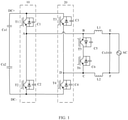
- HERIC topologies generated based on a highly efficient and reliable inverter concept (HERIC) are widely used in photovoltaic inverter products thanks to its low costs. As shown in FIG.
- a HERIC topology in the conventional technology, includes a first longitudinal bridge and a second longitudinal bridge. Two ends of the first longitudinal bridge are respectively connected to a first switching transistor and a second switching transistor. Two ends of the second longitudinal bridge are respectively connected to a third switching transistor and a fourth switching transistor. In an upper half cycle of inverter output, the first switching transistor and the fourth switching transistor are turned on. In a freewheeling phase, the first switching transistor and the fourth switching transistor are simultaneously turned off. In practice, turn-off speeds of the first switching transistor and the fourth switching transistor cannot maintain completely consistent. For example, a turn-off speed of the fourth switching transistor is faster than that of the first switching transistor. In this case, a voltage on a bus, the first longitudinal bridge, and the second longitudinal bridge increases.
- EMC electro magnetic compatibility
- the HERIC topology in the conventional technology still needs to be improved.
- Embodiments of this application provide an inverter circuit, an inverter, and a photovoltaic power system.
- a solution in which a capacitor is bridge-connected to a bus at a location of a connection point between a longitudinal bridge and a transverse bridge in a HERIC topology can suppress resonance caused by different turn-off speeds of switching transistors when a power circuit works normally.
- a first aspect of this application provides an inverter circuit, including a bus, a first longitudinal bridge, a second longitudinal bridge, a transverse bridge, and a filter.
- a capacitor group is disposed on the bus, the bus is connected in parallel to a direct current power supply, and the capacitor group includes a first capacitor and a second capacitor that are disposed in series.
- the first capacitor is disposed on a side that is of the bus and that is connected to a positive electrode of the direct current power supply
- the second capacitor is disposed on a side that is of the bus and that is connected to a negative electrode of the direct current power supply
- the first capacitor and the second capacitor are configured to be charged by the direct current power supply, to provide a direct current voltage to the first longitudinal bridge, the second longitudinal bridge, and the transverse bridge.
- the bus is connected in parallel to the first longitudinal bridge, the first longitudinal bridge is connected in parallel to the second longitudinal bridge, the first longitudinal bridge includes a first switching transistor and a second switching transistor that are connected in series, the second longitudinal bridge includes a third switching transistor and a fourth switching transistor that are connected in series, and two ends of the transverse bridge are respectively connected to the first longitudinal bridge and the second longitudinal bridge.
- the filter is connected in parallel to the transverse bridge, the filter is connected to an alternating current power grid, and the transverse bridge is configured to supply power to the alternating current power grid by using the filter.
- the inverter circuit further includes: a third capacitor, where the third capacitor is connected between the bus and the first longitudinal bridge, and a connection point between the third capacitor and the first longitudinal bridge is located between the first switching transistor and the second switching transistor; and a fourth capacitor, where the fourth capacitor is connected between the bus and the second longitudinal bridge, and a connection point between the fourth capacitor and the second longitudinal bridge is located between the third switching transistor and the fourth switching transistor.
- the first switching transistor, the second switching transistor, the third switching transistor, and the fourth switching transistor may be MOS transistors or IGBT devices.
- the third capacitor and the fourth capacitor are respectively bridge-connected between the first longitudinal bridge and the bus and between the second longitudinal bridge and the bus, so that in a process in which the first switching transistor and the fourth switching transistor are turned off, the third capacitor can stabilize a voltage difference generated by different turn-off speeds of the two switching transistors. This prevents a resonance phenomenon, and effectively avoids an EMC problem caused by the resonance phenomenon.
- the fourth capacitor can stabilize a voltage difference generated by different turn-off speeds of the two switching transistors. This stabilizes a voltage in a negative half cycle of converting a direct current into an alternating current, and prevents the resonance phenomenon.
- At least one inductor is disposed in series on a line on which the third capacitor is located, and/or at least one inductor is disposed in series on a line on which the fourth capacitor is located.
- the at least one inductor connected in series to the third capacitor and/or the at least one inductor connected in series to the fourth capacitor can protect the third capacitor and/or the fourth capacitor in a charging and discharging process.
- At least one resistor is disposed in series on a line on which the third capacitor is located, and/or at least one resistor is disposed in series on a line on which the fourth capacitor is located.
- the at least one resistor connected in series to the third capacitor and/or the at least one resistor connected in series to the fourth capacitor can protect the third capacitor and/or the fourth capacitor by charging and discharging a current in a charging and discharging process.
- At least one inductor and at least one resistor are disposed in series on a line on which the third capacitor is located, and/or at least one inductor and at least one resistor are disposed in series on a line on which the fourth capacitor is located.
- the at least one resistor and the at least one inductor that are connected in series to the third capacitor and/or the at least one resistor and the at least one inductor that are connected in series to the fourth capacitor can work together to protect the third capacitor and/or the fourth capacitor in a charging and discharging process.
- both a connection point between the line on which the third capacitor is located and the bus and a connection point between the line on which the fourth capacitor is located and the bus are disposed between the first capacitor and the second capacitor.
- both the third capacitor and the fourth capacitor are bridge-connected between the first capacitor and the second capacitor on the bus, so that the first capacitor and the third capacitor form a parallel circuit, and the second capacitor and the fourth capacitor form a parallel circuit.
- a voltage of the third capacitor is equal to a voltage of the first capacitor, stabilizing a voltage on the bus, the first longitudinal bridge, and the second longitudinal bridge in a positive half cycle of inverter output.
- a voltage of the fourth capacitor is equal to a voltage of the second capacitor, stabilizing a voltage on the bus, the first longitudinal bridge, and the second longitudinal bridge in a negative half cycle of inverter output. This prevents resonance.
- the voltage of the first capacitor causes a circuit to sequentially pass through the third capacitor, a first inductor, the alternating current power grid, a second inductor, the fourth capacitor, and the second capacitor.
- the third capacitor and the fourth capacitor are charged with 1/2 bus voltage.
- a voltage discharged by the third capacitor or the fourth capacitor and a voltage discharged by the first capacitor or the second capacitor are equal, and both are the 1/2 bus voltage. Therefore, a circuit loss is relatively small. This not only can effectively prevent resonance caused by different turn-on/turn-off speeds, but also can effectively reduce a circuit loss.
- neither a connection point between the line on which the third capacitor is located and the bus nor a connection point between the line on which the fourth capacitor is located and the bus is disposed between the first capacitor and the second capacitor.
- the connection point between the line on which the third capacitor is located and the bus and the connection point between the line on which the fourth capacitor is located and the bus both are disposed between the first capacitor and the direct current power supply.
- the connection point between the line on which the third capacitor is located and the bus and the connection point between the line on which the fourth capacitor is located and the bus both are disposed between the second capacitor and the direct current power supply.
- connection point between the line on which the third capacitor is located and the bus is disposed between the first capacitor and the direct current power supply
- the connection point between the line on which the fourth capacitor is located and the bus is disposed between the second capacitor and the direct current power supply.
- the connection point between the line on which the third capacitor is located and the bus is disposed between the second capacitor and the direct current power supply
- the connection point between the line on which the fourth capacitor is located and the bus is disposed between the first capacitor and the direct current power supply.
- neither a bridge -connection point of the third capacitor nor a bridge -connection point of the fourth capacitor is disposed between the first capacitor and the second capacitor.
- the third capacitor can absorb a voltage fluctuation. This stabilizes a circuit.
- the fourth capacitor can absorb a voltage fluctuation. This stabilizes a circuit. Therefore, resonance caused by different turn-on/turn-off speeds can be effectively prevented.
- connection point between the line on which the third capacitor is located and the bus and a connection point between the line on which the fourth capacitor is located and the bus is disposed between the first capacitor and the second capacitor.
- the connection point between the third capacitor and the bus may be disposed between the first capacitor and the second capacitor
- the connection point between the line on which the fourth capacitor is located and the bus may be disposed between the first capacitor and the direct current power supply or between the second capacitor and the direct current power supply.
- connection point between the fourth capacitor and the bus may be disposed between the first capacitor and the second capacitor, and the connection point between the line on which the third capacitor is located and the bus may be disposed between the first capacitor and the direct current power supply or between the second capacitor and the direct current power supply.
- one of the third capacitor or the fourth capacitor is bridge-connected between the first capacitor and the second capacitor, and the other capacitor is bridge-connected between the capacitor group and the direct current power supply, so that the third capacitor can absorb a voltage fluctuation at a moment at which the first switching transistor and the fourth switching transistor are turned off. This stabilizes a circuit.
- the fourth capacitor can absorb a voltage fluctuation at a moment at which the second switching transistor and the third switching transistor are turned off. This can effectively prevent resonance caused by different turn-on/turn-off speeds, but causes a specific circuit loss.
- the filter includes the first inductor and the second inductor
- the transverse bridge includes a freewheeling switch group.
- the first inductor is connected between the first longitudinal bridge and the alternating current power grid
- the second inductor is connected between the alternating current power grid and the second longitudinal bridge
- the freewheeling switch group is connected in parallel between the first inductor and the second inductor.
- the inverter circuit further includes a fifth capacitor.
- the fifth capacitor is connected in parallel between the first inductor and the second inductor, and the fifth capacitor is configured to stabilize a voltage of the filter.
- the freewheeling switch group includes a fifth switching transistor and a sixth switching transistor that are connected in series.
- the fifth switching transistor and the sixth switching transistor may be MOS transistors or IGBT devices.
- the fifth switching transistor and the sixth switching transistor are controlled to control a circuit from a starting phase to a freewheeling phase, so that the first inductor and the second inductor that are excited are connected to the alternating current power grid.
- the capacitors may be bridge-connected to the bus on the first longitudinal bridge and the second longitudinal bridge.
- the capacitors bridge-connected to the bus can stabilize a voltage fluctuation caused by different turn-off speeds of the switching transistors, and suppress the resonance caused by different turn-on/turn-off speeds of the switching transistors when a power circuit works normally. This resolves an EMC-related problem caused by the resonance.
- a second aspect of this application provides an inverter, including a control unit and an inverter power unit, where the control unit is configured to control work of the inverter power unit, and the inverter power unit includes the inverter circuit according to the first aspect or any possible implementations of the first aspect.
- capacitors may be bridge-connected to the bus on the first longitudinal bridge and the second longitudinal bridge.
- the capacitors bridge-connected to the bus can stabilize a voltage fluctuation caused by different turn-off speeds of the switching transistors, and suppress resonance caused by different turn-on/turn-off speeds of the switching transistors when a power circuit works normally.
- a third aspect of this application provides a photovoltaic power system, including a photovoltaic panel, an inverter, and an alternating current power grid, where the photovoltaic panel is connected to the inverter, and the inverter is connected to the alternating current power grid; the photovoltaic panel is configured to convert light energy into a direct current; the inverter includes the inverter circuit according to the first aspect or any possible implementations of the first aspect, and is configured to convert the direct current into an alternating current; the alternating current power grid is configured to transmit the alternating current.
- the inverter implements conversion from the direct current into the alternating current.
- capacitors may be bridge-connected to the bus on the first longitudinal bridge and the second longitudinal bridge. In this way, in a working process of the HERIC topology, when the first switching transistor and the fourth switching transistor are turned off or the second switching transistor and the third switching transistor are turned off, the capacitors bridge-connected to the bus can stabilize a voltage fluctuation caused by different turn-off speeds of the switching transistors, and suppress resonance caused by different turn-on/turn-off speeds of the switching transistors when a power circuit works normally.
- Inverters are apparatuses that convert a direct current into an alternating current, and have been rapidly developing in recent years with the development of photovoltaic power industry.
- a photovoltaic power system includes a plurality of components, such as a photovoltaic module, an inverter, a transformer, and a cable.
- the inverter is a core component for energy conversion of the photovoltaic power system, and converts a direct current output by the photovoltaic module into an alternating current available for a grid.
- inverters are also widely used in other systems that need to convert a direct current into an alternating current.
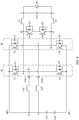
- a HERIC topology includes a first longitudinal bridge 10 and a second longitudinal bridge 20. Two ends of the first longitudinal bridge 10 are respectively connected to a first switching transistor T1 and a second switching transistor T2. Two ends of the second longitudinal bridge 20 are respectively connected to a third switching transistor T3 and a fourth switching transistor T4. In an upper half cycle of inverter output, the first switching transistor T1 and the fourth switching transistor T4 are turned on. When a freewheeling phase is entered, the first switching transistor T1 and the fourth switching transistor T4 are simultaneously turned off.
- a turn-off speed of the fourth switching transistor T4 is faster than that of the first switching transistor T1.
- a voltage on a bus, the first longitudinal bridge 10, and the second longitudinal bridge 20 increases. After the first switching transistor T1 is turned off, the voltage falls back. A resonance phenomenon occurs in this process. Consequently, impact is exerted on electromagnetic compatibility (electro magnetic compatibility, EMC) for a device and a system to work normally in their electromagnetic environment without causing unacceptable electromagnetic interference to anything in the environment. As a result, conduction and radiation test results of the EMC exceed thresholds.
- EMC electro magnetic compatibility
- an embodiment of this application provides an inverter circuit.
- a solution in which a capacitor is bridge-connected to a bus at a location of a connection point between a longitudinal bridge and a transverse bridge in a HERIC topology can suppress resonance caused by different turn-off speeds of switching transistors when a power circuit works normally.
- the inverter circuit and the inverter provided in the embodiments of this application may be a photovoltaic inverter used in a photovoltaic power system, or may be used in another circuit or apparatus that needs to convert a direct current into an alternating current. This is not limited in the embodiments of this application.
- a photovoltaic inverter is used as an example in this embodiment of this application to describe in detail the inverter provided in this embodiment of this application.
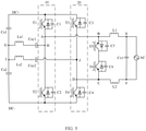
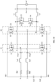
- the inverter circuit As shown in FIG. 1 , based on the HERIC topology in the conventional technology, the inverter circuit provided in this embodiment of this application specifically includes the bus, the first longitudinal bridge 10, the second longitudinal bridge 20, a transverse bridge, and a filter.
- a capacitor group is disposed on the bus, the bus is connected in parallel to a direct current power supply, and the capacitor group includes a first capacitor Cs1 and a second capacitor Cs2 that are disposed in series.
- the first capacitor Cs1 is connected to a positive electrode DC+ of the direct current power supply
- the second capacitor Cs2 is connected to a negative electrode DC- of the direct current power supply
- the first capacitor Cs1 and the second capacitor Cs2 are configured to be charged by the direct current power supply to provide a direct current voltage to the first longitudinal bridge 10, the second longitudinal bridge 20, and the transverse bridge.
- the bus is connected in parallel to the first longitudinal bridge 10, the first longitudinal bridge 10 is connected in parallel to the second longitudinal bridge 20, the first longitudinal bridge 10 includes a first switching transistor T1 and a second switching transistor T2 that are connected in series, and a line that connects the first switching transistor T1 and the second switching transistor T2.
- the second longitudinal bridge 20 includes a third switching transistor T3 and a fourth switching transistor T4 that are connected in series, and a line that connects the third switching transistor T3 and the fourth switching transistor T4.
- Two ends of the transverse bridge are respectively connected to the first longitudinal bridge 10 and the second longitudinal bridge 20.
- the transverse bridge specifically includes a circuit structure that sequentially passes through a connection point A, a connection point B, a connection point C, and a connection point D.
- connection point A is a connection point between the transverse bridge and a first bridge arm 10
- connection point D is a connection point between the transverse bridge and a second bridge arm 20.
- first longitudinal bridge 10 and the second longitudinal bridge 20 are not limited to the foregoing structure, and may also be a related topology structure variant.
- first longitudinal bridge 10 or the second longitudinal bridge 20 has more than two switching transistors.
- the transverse bridge is also not limited to the foregoing structure, but may also be a related topology structure variant such as a topology structure including a part of the structure of the transverse bridge. This is not limited in this embodiment of this application.
- a source of the first switching transistor T1 is connected to a drain of the second switching transistor T2 through a wire
- a drain of the first switching transistor T1 is connected to the first capacitor Cs1 through a wire
- a source of the second switching transistor T2 is connected to the second capacitor Cs2 through a wire.
- the first switching transistor T1, the second switching transistor T2, the third switching transistor T3, and the fourth switching transistor T4 may be MOS transistors, IGBT devices, or other semiconductor devices that have a switching function. This is not limited in this embodiment of this application.
- the first switching transistor T1, the second switching transistor T2, the third switching transistor T3, and the fourth switching transistor T4 are MOS transistors
- a diode and a capacitor may be connected in parallel to each switching transistor.
- a capacitor C1, a capacitor C2, a capacitor C3, and a capacitor C4 may be respectively connected in parallel to the first switching transistor T1, the second switching transistor T2, the third switching transistor T3, and the fourth switching transistor T4.
- the MOS transistors may be gallium nitride MOS transistors or silicon carbide MOS transistors.
- the first capacitor Cs1 or the second capacitor Cs2 may be implemented by using one capacitor, or may be implemented by using a plurality of capacitors. This is not limited in this embodiment of this application.
- the filter is connected in parallel to the transverse bridge, the filter is connected to an alternating current power grid AC, and the transverse bridge is configured to supply power to the alternating current power grid AC by using the filter.
- the filter specifically includes a circuit structure that sequentially passes through a connection point B, a connection point E, a connection point F, and a connection point C.
- the filter is connected in parallel to the transverse bridge through the connection point B and the connection point C, and the filter is connected to the alternating current power grid AC through the connection point E and the connection point F.
- the filter includes a first inductor L1 and a second inductor L2, and the transverse bridge includes a freewheeling switch group.
- the first inductor L1 is connected between the first longitudinal bridge 10 and the alternating current power grid AC
- the second inductor L2 is connected between the alternating current power grid AC and the second longitudinal bridge 20
- the freewheeling switch group is connected in parallel between the first inductor L1 and the second inductor L2.
- the first inductor L1 is connected to the transverse bridge through the connection point B
- the second inductor L2 is connected to the transverse bridge through the connection point C
- the first inductor L1 and the second inductor L2 are respectively connected to the alternating current power grid AC through the connection point E and the connection point F.
- the first inductor L1 and the second inductor L2 are excited by the direct current power supply when the first switching transistor T1 and the fourth switching transistor T4 are turned on or the second switching transistor T2 and the third switching transistor T3 are turned on.
- the freewheeling switch group is turned on when the first switching transistor T1 and the fourth switching transistor T4 are turned off or the second switching transistor T2 and the third switching transistor T3 are turned off, so that the first inductor L1 and the second inductor L2 supply power to the output.
- the freewheeling switch group includes a fifth switching transistor T5 and a sixth switching transistor T6 that are connected in series.
- the fifth switching transistor T5 is configured to maintain a turned-on state.
- the sixth switching transistor T6 is turned on when the first switching transistor T1 and the fourth switching transistor T4 are turned off or the second switching transistor T2 and the third switching transistor T3 are turned off, so that the first inductor L1 and the second inductor L2 supply power to the output.
- the inverter further includes a fifth capacitor Cx1.
- the fifth capacitor Cx1 is connected in parallel between the first inductor L1 and the second inductor L2 through the connection point E and the connection point F, and the fifth capacitor Cx1 is configured to stabilize a voltage of the transverse bridge, so that the transverse bridge outputs a stable voltage to the alternating current power grid AC.
- the fifth switching transistor T5 and the sixth switching transistor T6 are MOS transistors, and the MOS transistors may be MOS transistors, IGBT devices, or other semiconductor devices that have a switching function. This is not limited in this embodiment of this application.
- the fifth switching transistor T5 and the sixth switching transistor T6 are MOS transistors, a diode and a capacitor C5 may be connected in parallel to the fifth switching transistor T5, and a diode and a capacitor C6 may be connected in parallel to the sixth switching transistor T6.
- the MOS transistors may be gallium nitride MOS transistors or silicon carbide MOS transistors.
- a topology structure on which the inverter circuit in this embodiment of this application is based may be a related topology structure variant of the HERIC topology in addition to the foregoing HERIC topology. This is not limited in this embodiment of this application.
- the direct current power supply charges the first capacitor Cs1 and the second capacitor Cs2 on the bus because the bus is connected in parallel to the direct current power supply.
- the first switching transistor T1 and the fourth switching transistor T4 are turned on.
- the first capacitor Cs1 releases the voltage through a positive electrode DC+ of the bus.
- a current sequentially passes through the first switching transistor T1, the first inductor L1, the second inductor L2, and the fourth switching transistor T4, and finally flows to a negative electrode DC- of the bus, to complete a loop.
- the first inductor L1 and the second inductor L2 are charged to excite the first inductor L1 and the second inductor L2.
- the first switching transistor T1 and the fourth switching transistor T4 are turned off, and the freewheeling switch group is turned on.
- a specific turn-on implementation of the freewheeling switch group is as follows: The fifth switching transistor T5 always maintains a turn-on state; when the freewheeling switch group needs to change from turn-off to turn-on, the sixth switching transistor T6 changes from turn-off to turn-on, so as to turn on the freewheeling switch group.
- the first inductor L1 and the second inductor L2 discharge, and a current forms a loop among the alternating current power grid AC, the first inductor L1, the freewheeling switch group, and the second inductor L2. In this way, in the freewheeling phase, the first inductor L1 and the second inductor L2 continuously charge the alternating current power grid AC, so that the transverse bridge supplies power to the output in a positive half cycle of the alternating current.
- the second switching transistor T2 and the third switching transistor T3 are turned on.
- the second capacitor Cs2 releases a voltage through the negative electrode DC- of the bus.
- a current sequentially passes through the second switching transistor T2, the first inductor L1, the second inductor L2, and the third switching transistor T3, and finally flows to the positive electrode DC+ of the bus, to complete a loop.
- the first inductor L1 and the second inductor L2 are charged to excite the first inductor L1 and the second inductor L2.
- the second switching transistor T2 and the third switching transistor T3 are turned off, and the freewheeling switch group is turned on.
- a specific turn-on implementation of the freewheeling switch group is as follows: The fifth switching transistor T5 always maintains a turn-on state; when the freewheeling switch group needs to change from turn-off to turn-on, the sixth switching transistor T6 changes from turn-off to turn-on, so as to turn on the freewheeling switch group.
- the first inductor L1 and the second inductor L2 discharge, and a current forms a loop among the alternating current power grid AC, the first inductor L1, the freewheeling switch group, and the second inductor L2. In this way, in the freewheeling phase, the first inductor L1 and the second inductor L2 continuously charge the alternating current power grid AC, so that the transverse bridge supplies power to the output in a negative half cycle of the alternating current.
- the inverter circuit in the HERIC topology converts a direct current output by the direct current power supply into an alternating current, to supply power to the alternating current power grid AC.
- a turn-off speed of the first switching transistor T1 cannot be synchronized with a turn-off speed of the fourth switching transistor T4.
- the turn-off speed of the fourth switching transistor T4 is faster than the turn-off speed of the first switching transistor T1.
- EMC electro magnetic compatibility
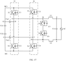
- a third capacitor Csy1 and a fourth capacitor Csy2 are bridge-connected to the inverter circuit provided in this embodiment of this application based on the existing HERIC topology.
- the third capacitor Csy 1 is connected between the bus and the first longitudinal bridge 10, and a connection point H between the third capacitor Csy 1 and the first longitudinal bridge 10 is located between the first switching transistor T1 and the second switching transistor T2.
- the fourth capacitor Csy2 is connected between the bus and the second longitudinal bridge 20, and a connection point J between the fourth capacitor Csy2 and the second longitudinal bridge 20 is located between the third switching transistor T3 and the fourth switching transistor T4.
- the third capacitor Csy1 is configured to stabilize the voltage on the bus, the first longitudinal bridge 10, and the second longitudinal bridge 20 when the first switching transistor T1 and the fourth switching transistor T4 are turned off.
- the fourth capacitor Csy2 is configured to stabilize the voltage on the bus, the first longitudinal bridge 10, and the second longitudinal bridge 20 when the second switching transistor T2 and the third switching transistor T3 are turned off.
- a connection point G between the third capacitor Csy 1 and the bus is disposed between the first capacitor Cs1 and the second capacitor Cs2, and the third capacitor Csy1 is connected to the first longitudinal bridge 10 through the connection point H.
- a connection point I between the fourth capacitor Csy2 and the bus is disposed between the first capacitor Cs1 and the second capacitor Cs2, and the fourth capacitor Csy2 is connected to the second longitudinal bridge 20 through the connection point J.
- the first switching transistor T1 and the fourth switching transistor T4 are turned on.
- the first capacitor Cs1 and the third capacitor Csy 1 form a parallel equivalent circuit.
- the first capacitor Cs1 charges the third capacitor Csy1, and voltages of the first capacitor Cs1 and the third capacitor Csy1 are equal.
- the first capacitor Cs1 and the second capacitor Cs2 form a voltage divider circuit of the direct current power supply, the voltages of the first capacitor Cs1 and the second capacitor Cs2 each are equal to 1/2 of the bus voltage, that is, the 1/2 bus voltage. In this case, the voltage of the third capacitor Csy1 is also equal to the 1/2 bus voltage.
- the first switching transistor T1 and the fourth switching transistor T4 are turned off. If the turn-off speed of the fourth switching transistor T4 is faster than the turn-off speed of the first switching transistor T1, the third capacitor Csy 1 can be further charged by a capacitor with the positive voltage of the bus when the fourth switching transistor T4 is turned off but the first switching transistor T1 is not turned off, to avoid fluctuations caused by a voltage increase.
- the 1/2 bus voltage output by the third capacitor Csy1 can play a stabilizing role, preventing a fluctuation caused by the voltage increase on the bus, the first longitudinal bridge 10, and the second longitudinal bridge 20. This effectively prevents resonance caused by the different turn-off speeds of the first switching transistor T1 and the fourth switching transistor T4 in the working process of the inverter circuit in the HERIC topology.
- the second switching transistor T2 and the third switching transistor T3 are turned on.
- the second capacitor Cs2 and the fourth capacitor Csy2 form a parallel equivalent circuit.
- the second capacitor Cs2 charges the fourth capacitor Csy2, and voltages of the second capacitor Cs2 and the fourth capacitor Csy2 are equal.
- the first capacitor Cs1 and the second capacitor Cs2 form a voltage divider circuit of the direct current power supply, the voltages of the first capacitor Cs1 and the second capacitor Cs2 each are equal to 1/2 of the bus voltage, that is, the 1/2 bus voltage.
- the voltage of the fourth capacitor Csy2 is also equal to the 1/2 bus voltage.
- the second switching transistor T2 and the third switching transistor T3 are turned off. If the turn-off speed of the third switching transistor T3 is faster than the turn-off speed of the second switching transistor T2, the fourth capacitor Csy2 can be further charged by a capacitor with the positive voltage of the bus when the third switching transistor T3 is turned off but the second switching transistor T2 is not turned off, to avoid fluctuations caused by a voltage increase.
- the 1/2 bus voltage output by the fourth capacitor Csy2 can play a stabilizing role when the second switching transistor T2 is turned off but the third switching transistor T3 is not turned off, preventing a fluctuation caused by the voltage increase on the bus, the first longitudinal bridge 10, and the second longitudinal bridge 20. This effectively prevents resonance caused by the different turn-off speeds of the second switching transistor T2 and the third switching transistor T3 in a working process of the inverter in the HERIC topology.
- a difference between the positive half cycle and the negative half cycle of inverter output lies in: In the positive half cycle, the first capacitor Cs1 is charged by the positive electrode DC+ of the direct current power supply, and charges the third capacitor Csy 1 with a 1/2 positive bus voltage; whereas in the negative half cycle, the second capacitor Cs2 is charged by the negative electrode DC- of the direct current power supply, and charges the fourth capacitor Csy2 with a 1/2 negative bus voltage.
- the third capacitor Csy 1 and the fourth capacitor Csy2 are bridge-connected between the first capacitor Cs1 and the second capacitor Cs2 on the bus.
- the first capacitor Cs1 and the third capacitor Csy 1 form a parallel circuit
- the second capacitor Cs2 and the fourth capacitor Csy2 form a parallel circuit.
- the voltage of the third capacitor Csy1 is equal to the voltage of the first capacitor Cs1, stabilizing the voltage on the bus, the first longitudinal bridge 10, and the second longitudinal bridge 20 in the positive half cycle of inverter output.
- the voltage of the fourth capacitor Csy2 is equal to the voltage of the second capacitor Cs2, stabilizing the voltage on the bus, the first longitudinal bridge 10, and the second longitudinal bridge 20 in the negative half cycle of inverter output. This prevents resonance.
- the voltage of the first capacitor Cs1 causes a circuit to sequentially pass through the third capacitor Csy1, the first inductor L1, the alternating current power grid AC, the second inductor L2, the fourth capacitor Csy2, and the second capacitor Cs2.
- the third capacitor Csy 1 and the fourth capacitor Csy2 are charged with 1/2 bus voltage.
- a voltage discharged by the third capacitor Csy 1 or the fourth capacitor Csy2 and a voltage discharged by the first capacitor Cs1 or the second capacitor Cs2 are equal and both are the 1/2 bus voltage. Therefore, a circuit loss is relatively small.
- the first implementation in this embodiment of this application not only can effectively prevent resonance caused by different turn-on/turn-off speeds, but also can effectively reduce a circuit loss. Therefore, the first implementation is a most preferred implementation.
- the third capacitor Csy 1 or the fourth capacitor Csy2 may be implemented by using one capacitor, or may be implemented by using a plurality of capacitors. This is not limited in this embodiment of this application.
- connection point G between the third capacitor Csy 1 and the bus and the connection point I between the fourth capacitor Csy2 and the bus are connected to the bus are merely the first implementation provided in this embodiment of this application.
- different working modes may be used to stabilize the voltage on the bus, the first longitudinal bridge 10, and the second longitudinal bridge 20 based on different locations of the connection point.
- the working modes further include:
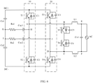
- connection point G between the third capacitor Csy1 and the bus is disposed between the first capacitor Cs1 and the positive electrode of the direct current power supply, and the third capacitor Csy1 is connected to the first longitudinal bridge 10 through the connection point H.
- connection point I between the fourth capacitor Csy2 and the bus is disposed between the first capacitor Cs1 and the positive electrode of the direct current power supply, and the fourth capacitor Csy2 is connected to the second longitudinal bridge 20 through the connection point J.
- the first switching transistor T1 and the fourth switching transistor T4 are turned on.
- a current starts from the first capacitor Cs1, and sequentially passes through the first switching transistor T1, the first inductor L1, the alternating current power grid AC, the second inductor L2, the fourth switching transistor T4, and the second capacitor Cs2.
- the first switching transistor T1 and the fourth switching transistor T4 are turned off.
- the turn-off speed of the fourth switching transistor T4 is different from the turn-off speed of the first switching transistor T1
- the generated positive voltage of the bus charges the third capacitor Csy1, so that the third capacitor Csy1 can absorb an increased voltage on the bus, the first longitudinal bridge 10, and the second longitudinal bridge 20, and a fluctuation caused by the voltage increase is avoided.
- the second switching transistor T2 and the third switching transistor T3 are turned on.
- a current starts from the second capacitor Cs2, and sequentially passes through the second switching transistor T2, the first inductor L1, the alternating current power grid AC, the second inductor L2, the third switching transistor T3, and the first capacitor Cs1.
- the second switching transistor T2 and the third switching transistor T3 are turned off.
- the turn-off speed of the second switching transistor T2 is different from the turn-off speed of the third switching transistor T3, the generated negative voltage of the bus charges the fourth capacitor Csy2, so that the fourth capacitor Csy2 can absorb a voltage change on the bus, the first longitudinal bridge 10, and the second longitudinal bridge 20, and a fluctuation caused by the voltage change is avoided. This effectively prevents resonance caused by the different turn-off speeds of the second switch and the third switch in the working process of the inverter circuit in the HERIC topology.
- the third capacitor Csy 1 and the fourth capacitor Csy2 are bridge-connected to a positive voltage location of the bus, so that the third capacitor Csy 1 can absorb a voltage fluctuation at a moment at which the first switching transistor T1 and the fourth switching transistor T4 are turned off, thereby stabilizing a circuit.
- the fourth capacitor Csy2 can absorb a voltage fluctuation at a moment at which the second switching transistor T2 and the third switching transistor T3 are turned off, thereby stabilizing the circuit.
- the voltage of the first capacitor Cs1 causes a circuit to sequentially pass through the third capacitor Csy 1 and the fourth capacitor Csy2, and flow through an entire loop.
- the third capacitor Csy1 and the fourth capacitor Csy2 are charged with one bus voltage.
- a voltage discharged by the third capacitor Csy 1 or the fourth capacitor Csy2 is greater than a voltage discharged by the first capacitor Cs1 or the second capacitor Cs2 (as described above, in the voltage divider circuit including the first capacitor Cs1 and the second capacitor Cs2, the voltage of the first capacitor Cs1 and the voltage of the second capacitor Cs2 both are equal to 1/2 bus voltage).
- the third capacitor Csy1 or the fourth capacitor Csy2 needs to discharge an extra voltage.
- Both the third capacitor Csy 1 and the fourth capacitor Csy2 are bridge-connected between the second capacitor Cs2 on the bus and the negative electrode of the direct current power supply.
- connection point G between the third capacitor Csy 1 and the bus is disposed between the second capacitor Cs2 and the negative electrode of the direct current power supply, and the third capacitor Csy 1 is connected to the first longitudinal bridge 10 through the connection point H.
- the connection point I between the fourth capacitor Csy2 and the bus is disposed between the second capacitor Cs2 and the negative electrode of the direct current power supply, and the fourth capacitor Csy2 is connected to the second longitudinal bridge 20 through the connection point J.
- the first switching transistor T1 and the fourth switching transistor T4 are turned on.
- a current starts from the first capacitor Cs1, and sequentially passes through the first switching transistor T1, the first inductor L1, the alternating current power grid AC, the second inductor L2, the fourth switching transistor T4, and the second capacitor Cs2.
- the first switching transistor T1 and the fourth switching transistor T4 are turned off.
- the turn-off speed of the fourth switching transistor T4 is different from the turn-off speed of the first switching transistor T1
- the generated positive voltage of the bus charges the third capacitor Csy1, so that the third capacitor Csy1 can absorb an increased voltage on the bus, the first longitudinal bridge 10, and the second longitudinal bridge 20, and a fluctuation caused by the voltage increase is avoided.
- the second switching transistor T2 and the third switching transistor T3 are turned on.
- a current starts from the second capacitor Cs2, and sequentially passes through the second switching transistor T2, the first inductor L1, the alternating current power grid AC, the second inductor L2, the third switching transistor T3, and the first capacitor Cs1.
- the second switching transistor T2 and the third switching transistor T3 are turned off.
- the turn-off speed of the second switching transistor T2 is different from the turn-off speed of the third switching transistor T3, the generated negative voltage of the bus charges the fourth capacitor Csy2, so that the fourth capacitor Csy2 can absorb a voltage change on the bus, the first longitudinal bridge 10, and the second longitudinal bridge 20, and a fluctuation caused by the voltage change is avoided. This effectively prevents resonance caused by the different turn-off speeds of the second switch and the third switch in the working process of the inverter circuit in the HERIC topology.
- the third capacitor Csy1 and the fourth capacitor Csy2 are bridge-connected to a negative voltage location of the bus, so that the third capacitor Csy 1 can absorb a voltage fluctuation at a moment at which the first switching transistor T1 and the fourth switching transistor T4 are turned off, thereby stabilizing a circuit.
- the fourth capacitor Csy2 can absorb a voltage fluctuation at a moment at which the second switching transistor T2 and the third switching transistor T3 are turned off, thereby stabilizing the circuit.
- the voltage of the first capacitor Cs1 causes a circuit to sequentially pass through the third capacitor Csy 1 and the fourth capacitor Csy2, and flow through an entire loop.
- the third capacitor Csy 1 and the fourth capacitor Csy2 are charged with the voltage of the one bus.
- the voltage discharged by the third capacitor Csy 1 or the voltage discharged by the fourth capacitor Csy2 is greater than the voltage discharged by the first capacitor Cs1 or the second capacitor Cs2 (as described above, in the voltage divider circuit including the first capacitor Cs1 and the second capacitor Cs2, the voltage of the first capacitor Cs1 and the voltage of the second capacitor Cs2 both are equal to 1/2 bus voltage).
- the third capacitor Csy 1 or the fourth capacitor Csy2 needs to discharge an extra voltage. This process causes an external circuit loss.
- the third implementation in this embodiment of this application can effectively prevent the resonance caused by the different turn-on/turn-off speeds, but causes a specific circuit loss.
- the third implementation and the foregoing second implementation of this application are equivalent.
- the third implementation may be used as an alternative solution of the foregoing second implementation.
- the third capacitor Csy 1 and the fourth capacitor Csy2 are bridge-connected between the first capacitor Cs1 and the second capacitor Cs2 (that is, a midpoint of the bus); in the second implementation, the third capacitor Csy 1 and the fourth capacitor Csy2 are bridge -connected between the first capacitor Cs1 and the positive electrode of the direct current power supply (that is, a positive electrode of the bus); in the third implementation, the third capacitor Csy1 and the fourth capacitor Csy2 are bridge -connected between the second capacitor Cs2 and the negative electrode of the direct current power supply (that is, a negative electrode of the bus).
- the following implementations may be further included based on a combination of the foregoing implementations.
- the third capacitor Csy1 is bridge-connected to the midpoint of the bus, and the fourth capacitor Csy2 is bridge-connected to the positive electrode of the bus.
- the third capacitor Csy1 is bridge -connected to the midpoint of the bus
- the fourth capacitor Csy2 is bridge-connected to the negative electrode of the bus.
- the fourth capacitor Csy2 is bridge-connected to the midpoint of the bus, and the third capacitor Csy 1 is bridge-connected to the positive electrode of the bus.
- the fourth capacitor Csy2 is bridge-connected to the midpoint of the bus, and the third capacitor Csy 1 is bridge-connected to the negative electrode of the bus.
- the third capacitor Csy1 is bridge-connected to the positive electrode of the bus
- the fourth capacitor Csy2 is bridge-connected to the negative electrode of the bus.
- the third capacitor Csy1 is bridge-connected to the negative electrode of the bus
- the fourth capacitor Csy2 is bridge-connected to the positive electrode of the bus.
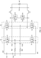
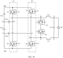
- an impedance network may be connected in series to the third capacitor Csy 1 and the fourth capacitor Csy2, to protect charging stability of the third capacitor Csy 1 and the fourth capacitor Csy2. In this way, in a process of charging the third capacitor Csy 1 and the fourth capacitor Csy2, the charging stability of the third capacitor Csy1 and the fourth capacitor Csy2 is maintained.
- the impedance network includes at least one inductor and/or at least one resistor that are connected in series. For ease of understanding, different cases of the impedance network are specifically described below with reference to the accompanying drawings.
- the inductor Ls1 and the inductor Ls2 are respectively disposed in series on the third capacitor Csy1 and the fourth capacitor Csy2.
- the inductor Ls1 is connected in series to the third capacitor Csy1, and the inductor Ls2 is connected in series to the fourth capacitor Csy2.
- the inductor Ls1 and the inductor Ls2 can share a current charged into the third capacitor Csy1 and the fourth capacitor Csy2, to prevent the third capacitor Csy1 and the fourth capacitor Csy2 from being damaged due to instantaneous charging of an excessive current.
- the inductor Ls1 and the inductor Ls2 may release the charged current, and slowly charge the third capacitor Csy1 and the fourth capacitor Csy2, so that a large current does not damage the third capacitor Csy1 and the fourth capacitor Csy2, and does not waste an excess current.
- a resistor Rs1 and a resistor Rs2 are respectively disposed in series on the third capacitor Csy 1 and the fourth capacitor Csy2.
- the resistor Rs1 is connected in series to the third capacitor Csy 1
- the resistor Rs2 is connected in series to the fourth capacitor Csy2.
- the resistor Rs1 and the resistor Rs2 respectively connected in series to the third capacitor Csy 1 and the fourth capacitor Csy2 can convert extra electric energy. This protects the third capacitor Csy 1 and the fourth capacitor Csy2, and prevents the third capacitor Csy 1 and the fourth capacitor Csy2 from being damaged due to charging of a large current.
- the inductor Ls1, the inductor Ls2, the resistor Rs1, and the resistor Rs2 are disposed in series on the third capacitor Csy 1 and the fourth capacitor Csy2.
- the inductor Ls1 and the resistor Rs1 are connected in series to the third capacitor Csy1, and the inductor Ls2 and the resistor Rs2 are connected in series to the fourth capacitor Csy2.
- the inductor Ls1 and the inductor Ls2 can share a current charged into the third capacitor Csy 1 and the fourth capacitor Csy2, to prevent the third capacitor Csy1 and the fourth capacitor Csy2 from being damaged due to instantaneous charging of an excessive current.
- the resistor Rs1 and the resistor Rs2 that are connected in series can convert extra electric energy. This further protects the third capacitor Csy1 and the fourth capacitor Csy2, and prevents the third capacitor Csy 1 and the fourth capacitor Csy2 from being damaged due to charging of a large current.
- the inductor Ls1 and the inductor Ls2 are respectively disposed in series on the third capacitor Csy1 and the fourth capacitor Csy2.
- the inductor Ls1 is connected in series to the third capacitor Csy 1, and the inductor Ls2 is connected in series to the fourth capacitor Csy2.
- the inductor Ls1 and the inductor Ls2 can share a current charged into the third capacitor Csy 1 and the fourth capacitor Csy2, to prevent the third capacitor Csy1 and the fourth capacitor Csy2 from being damaged due to instantaneous charging of an excessive current.
- the inductor Ls1 and the inductor Ls2 may release the charged current, and slowly charge the third capacitor Csy1 and the fourth capacitor Csy2, so that a large current does not damage the third capacitor Csy1 and the fourth capacitor Csy2, and does not waste an excess current.
- the resistor Rs1 and the resistor Rs2 are respectively disposed in series on the third capacitor Csy1 and the fourth capacitor Csy2.
- the resistor Rs1 is connected in series to the third capacitor Csy1, and the resistor Rs2 is connected in series to the fourth capacitor Csy2.
- the resistor Rs1 and the resistor Rs2 respectively connected in series to the third capacitor Csy 1 and the fourth capacitor Csy2 can convert extra electric energy. This protects the third capacitor Csy 1 and the fourth capacitor Csy2, and prevents the third capacitor Csy 1 and the fourth capacitor Csy2 from being damaged due to charging of a large current.
- the inductor Ls1, the inductor Ls2, the resistor Rs1, and the resistor Rs2 are disposed in series on the third capacitor Csy1 and the fourth capacitor Csy2.
- the inductor Ls1 and the resistor Rs1 are connected in series to the third capacitor Csy1, and the inductor Ls2 and the resistor Rs2 are connected in series to the fourth capacitor Csy2.
- the inductor Ls1 and the inductor Ls2 can share a current charged into the third capacitor Csy1 and the fourth capacitor Csy2, to prevent the third capacitor Csy1 and the fourth capacitor Csy2 from being damaged due to instantaneous charging of an excessive current.
- the resistor Rs1 and the resistor Rs2 that are connected in series can convert extra electric energy. This further protects the third capacitor Csy1 and the fourth capacitor Csy2, and prevents the third capacitor Csy 1 and the fourth capacitor Csy2 from being damaged due to charging of a large current.
- the inductor Ls1 and the inductor Ls2 are respectively disposed in series on the third capacitor Csy1 and the fourth capacitor Csy2.
- the inductor Ls1 is connected in series to the third capacitor Csy1, and the inductor Ls2 is connected in series to the fourth capacitor Csy2.
- the inductor Ls1 and the inductor Ls2 can share a current charged into the third capacitor Csy1 and the fourth capacitor Csy2, to prevent the third capacitor Csy1 and the fourth capacitor Csy2 from being damaged due to instantaneous charging of an excessive current.
- the inductor Ls1 and the inductor Ls2 may release the charged current, and slowly charge the third capacitor Csy1 and the fourth capacitor Csy2, so that a large current does not damage the third capacitor Csy1 and the fourth capacitor Csy2, and does not waste an excess current.
- the resistor Rs1 and the resistor Rs2 are respectively disposed in series on the third capacitor Csy1 and the fourth capacitor Csy2.
- the resistor Rs1 is connected in series to the third capacitor Csy1
- the resistor Rs2 is connected in series to the fourth capacitor Csy2.
- the resistor Rs1 and the resistor Rs2 respectively connected in series to the third capacitor Csy 1 and the fourth capacitor Csy2 can convert extra electric energy. This protects the third capacitor Csy 1 and the fourth capacitor Csy2, and prevents the third capacitor Csy 1 and the fourth capacitor Csy2 from being damaged due to charging of a large current.
- the inductor Ls1, the inductor Ls2, the resistor Rs1, and the resistor Rs2 are disposed in series on the third capacitor Csy1 and the fourth capacitor Csy2.
- the inductor Ls1 and the resistor Rs1 are connected in series to the third capacitor Csy 1, and the inductor Ls2 and the resistor Rs2 are connected in series to the fourth capacitor Csy2.
- the inductor Ls1 and the inductor Ls2 can share a current charged into the third capacitor Csy1 and the fourth capacitor Csy2, to prevent the third capacitor Csy1 and the fourth capacitor Csy2 from being damaged due to instantaneous charging of an excessive current.
- the resistor Rs1 and the resistor Rs2 that are connected in series can convert extra electric energy. This further protects the third capacitor Csy1 and the fourth capacitor Csy2, and prevents the third capacitor Csy 1 and the fourth capacitor Csy2 from being damaged due to charging of a large current.
- an impedance network may be disposed on the third capacitor Csy1 and the fourth capacitor Csy2.
- a difference lies only in different combinations of the bridge-connection modes. Details are not described herein again.
- the impedance network may protect the third capacitor Csy 1 and the fourth capacitor Csy2, and prevent the third capacitor Csy 1 and the fourth capacitor Csy2 from being damaged in a charging process.
- existence of the impedance network also reduces the third capacitor Csy1 and the fourth capacitor Csy2, thereby affecting protection of the third capacitor Csy1 and the fourth capacitor Csy2 against resonance in a turn-off process of the switching transistors to some extent. In this way, users can determine, depending on actual situations, whether to add an impedance network and to increase a quantity of capacitors specifically disposed in the impedance network and a quantity of inductors specifically disposed in the impedance network.
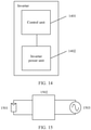
- an embodiment of this application further provides an inverter.
- the inverter includes a control unit 1401 and an inverter power unit 1402.
- the control unit is configured to control work of the inverter power unit, and the inverter power unit 1402 includes the inverter circuit according to any one of the foregoing implementations.
- the control unit 1401 may include a control chip and a circuit structure configured to implement a function of the control chip. Work of the control unit 1401 and the inverter power unit 1402 may include that the control unit 1401 controls turn-on or turn-off of each switching transistor of the inverter circuit in the inverter power unit 1402.
- an embodiment of this application further provides a photovoltaic power system, including a photovoltaic panel 1501, an inverter 1502, and an alternating current power grid 1503.
- the photovoltaic panel 1501 is connected to the inverter 1502, and the inverter 1502 is connected to the alternating current power grid 1503.
- the photovoltaic panel 1501 is configured to convert light energy into a direct current.
- the inverter 1502 includes the inverter circuit according to any one of the foregoing embodiments, and is configured to convert the direct current into an alternating current.
- the alternating current power grid 1503 is configured to transmit the alternating current.
- the inverter converts the direct current generated by the photovoltaic panel through solar energy power generation into the alternating current, and connects the alternating current to the alternating current power grid, so that solar energy is utilized.
- the inverter circuit included in the inverter is the inverter circuit according to any one of the foregoing embodiments. For understanding, refer to the foregoing description of the inverter circuit.
- the inverter circuit not only can convert the alternating current into the direct current, but also can avoid an EMC problem caused by a resonance phenomenon.
Abstract
Description
- This application claims priority to
Chinese Patent Application No. 201910469584.X, filed with the China National Intellectual Property Administration on May 31, 2019 - This application relates to the field of voltage conversion technologies, and in particular, to an inverter circuit, an inverter, and a photovoltaic power system.
- As a type of renewable clean energy, photovoltaic power industry has been developing rapidly in recent years. A photovoltaic power system includes a plurality of components, such as a photovoltaic module, an inverter, a transformer, and a cable. The inverter is a core component for energy conversion of the photovoltaic power system, and converts a direct current output by the photovoltaic module into an alternating current available for a grid. In addition, inverters are also widely used in other systems that need to convert a direct current into an alternating current. HERIC topologies generated based on a highly efficient and reliable inverter concept (HERIC) are widely used in photovoltaic inverter products thanks to its low costs. As shown in
FIG. 1 , in the conventional technology, a HERIC topology includes a first longitudinal bridge and a second longitudinal bridge. Two ends of the first longitudinal bridge are respectively connected to a first switching transistor and a second switching transistor. Two ends of the second longitudinal bridge are respectively connected to a third switching transistor and a fourth switching transistor. In an upper half cycle of inverter output, the first switching transistor and the fourth switching transistor are turned on. In a freewheeling phase, the first switching transistor and the fourth switching transistor are simultaneously turned off. In practice, turn-off speeds of the first switching transistor and the fourth switching transistor cannot maintain completely consistent. For example, a turn-off speed of the fourth switching transistor is faster than that of the first switching transistor. In this case, a voltage on a bus, the first longitudinal bridge, and the second longitudinal bridge increases. After the first switching transistor is turned off, the voltage falls back. A resonance phenomenon occurs in this process. Consequently, impact is exerted on electromagnetic compatibility (electro magnetic compatibility, EMC) for a device and a system to work normally in their electromagnetic environment without causing unacceptable electromagnetic interference to anything in the environment. As a result, conduction and radiation test results of the EMC exceed thresholds. - Therefore, the HERIC topology in the conventional technology still needs to be improved.
- Embodiments of this application provide an inverter circuit, an inverter, and a photovoltaic power system. A solution in which a capacitor is bridge-connected to a bus at a location of a connection point between a longitudinal bridge and a transverse bridge in a HERIC topology can suppress resonance caused by different turn-off speeds of switching transistors when a power circuit works normally.
- A first aspect of this application provides an inverter circuit, including a bus, a first longitudinal bridge, a second longitudinal bridge, a transverse bridge, and a filter. A capacitor group is disposed on the bus, the bus is connected in parallel to a direct current power supply, and the capacitor group includes a first capacitor and a second capacitor that are disposed in series. The first capacitor is disposed on a side that is of the bus and that is connected to a positive electrode of the direct current power supply, the second capacitor is disposed on a side that is of the bus and that is connected to a negative electrode of the direct current power supply, and the first capacitor and the second capacitor are configured to be charged by the direct current power supply, to provide a direct current voltage to the first longitudinal bridge, the second longitudinal bridge, and the transverse bridge. The bus is connected in parallel to the first longitudinal bridge, the first longitudinal bridge is connected in parallel to the second longitudinal bridge, the first longitudinal bridge includes a first switching transistor and a second switching transistor that are connected in series, the second longitudinal bridge includes a third switching transistor and a fourth switching transistor that are connected in series, and two ends of the transverse bridge are respectively connected to the first longitudinal bridge and the second longitudinal bridge. The filter is connected in parallel to the transverse bridge, the filter is connected to an alternating current power grid, and the transverse bridge is configured to supply power to the alternating current power grid by using the filter. The inverter circuit further includes: a third capacitor, where the third capacitor is connected between the bus and the first longitudinal bridge, and a connection point between the third capacitor and the first longitudinal bridge is located between the first switching transistor and the second switching transistor; and a fourth capacitor, where the fourth capacitor is connected between the bus and the second longitudinal bridge, and a connection point between the fourth capacitor and the second longitudinal bridge is located between the third switching transistor and the fourth switching transistor. The first switching transistor, the second switching transistor, the third switching transistor, and the fourth switching transistor may be MOS transistors or IGBT devices.
- In this embodiment, based on an existing inverter circuit in a HERIC topology, the third capacitor and the fourth capacitor are respectively bridge-connected between the first longitudinal bridge and the bus and between the second longitudinal bridge and the bus, so that in a process in which the first switching transistor and the fourth switching transistor are turned off, the third capacitor can stabilize a voltage difference generated by different turn-off speeds of the two switching transistors. This prevents a resonance phenomenon, and effectively avoids an EMC problem caused by the resonance phenomenon. Similarly, in a process in which the second switching transistor and the third switching transistor are turned off, the fourth capacitor can stabilize a voltage difference generated by different turn-off speeds of the two switching transistors. This stabilizes a voltage in a negative half cycle of converting a direct current into an alternating current, and prevents the resonance phenomenon.
- With reference to the first aspect, in a first possible implementation, at least one inductor is disposed in series on a line on which the third capacitor is located, and/or at least one inductor is disposed in series on a line on which the fourth capacitor is located.
- In this embodiment, the at least one inductor connected in series to the third capacitor and/or the at least one inductor connected in series to the fourth capacitor can protect the third capacitor and/or the fourth capacitor in a charging and discharging process.
- With reference to the first aspect, in a second possible implementation, at least one resistor is disposed in series on a line on which the third capacitor is located, and/or at least one resistor is disposed in series on a line on which the fourth capacitor is located.
- In this embodiment, the at least one resistor connected in series to the third capacitor and/or the at least one resistor connected in series to the fourth capacitor can protect the third capacitor and/or the fourth capacitor by charging and discharging a current in a charging and discharging process.
- With reference to the first aspect, in a third possible implementation, at least one inductor and at least one resistor are disposed in series on a line on which the third capacitor is located, and/or at least one inductor and at least one resistor are disposed in series on a line on which the fourth capacitor is located.
- In this embodiment, the at least one resistor and the at least one inductor that are connected in series to the third capacitor and/or the at least one resistor and the at least one inductor that are connected in series to the fourth capacitor can work together to protect the third capacitor and/or the fourth capacitor in a charging and discharging process.
- With reference to the first aspect and the first to the third possible implementations of the first aspect, in a fourth possible implementation, both a connection point between the line on which the third capacitor is located and the bus and a connection point between the line on which the fourth capacitor is located and the bus are disposed between the first capacitor and the second capacitor.
- In this embodiment, both the third capacitor and the fourth capacitor are bridge-connected between the first capacitor and the second capacitor on the bus, so that the first capacitor and the third capacitor form a parallel circuit, and the second capacitor and the fourth capacitor form a parallel circuit. In this way, when the first switching transistor and the fourth switching transistor are turned on, a voltage of the third capacitor is equal to a voltage of the first capacitor, stabilizing a voltage on the bus, the first longitudinal bridge, and the second longitudinal bridge in a positive half cycle of inverter output. When the second switching transistor and the third switching transistor are turned on, a voltage of the fourth capacitor is equal to a voltage of the second capacitor, stabilizing a voltage on the bus, the first longitudinal bridge, and the second longitudinal bridge in a negative half cycle of inverter output. This prevents resonance. Further, when the first switching transistor, the second switching transistor, the third switching transistor, and the fourth switching transistor are all turned off, the voltage of the first capacitor causes a circuit to sequentially pass through the third capacitor, a first inductor, the alternating current power grid, a second inductor, the fourth capacitor, and the second capacitor. In this case, the third capacitor and the fourth capacitor are charged with 1/2 bus voltage. When the first switching transistor and the fourth switching transistor are turned on, or the second switching transistor and the third switching transistor are turned on, a voltage discharged by the third capacitor or the fourth capacitor and a voltage discharged by the first capacitor or the second capacitor are equal, and both are the 1/2 bus voltage. Therefore, a circuit loss is relatively small. This not only can effectively prevent resonance caused by different turn-on/turn-off speeds, but also can effectively reduce a circuit loss.
- With reference to the first aspect and the first to the third possible implementations of the first aspect, in a fifth possible implementation, neither a connection point between the line on which the third capacitor is located and the bus nor a connection point between the line on which the fourth capacitor is located and the bus is disposed between the first capacitor and the second capacitor. Specifically, the connection point between the line on which the third capacitor is located and the bus and the connection point between the line on which the fourth capacitor is located and the bus both are disposed between the first capacitor and the direct current power supply. Alternatively, the connection point between the line on which the third capacitor is located and the bus and the connection point between the line on which the fourth capacitor is located and the bus both are disposed between the second capacitor and the direct current power supply. Alternatively, the connection point between the line on which the third capacitor is located and the bus is disposed between the first capacitor and the direct current power supply, and the connection point between the line on which the fourth capacitor is located and the bus is disposed between the second capacitor and the direct current power supply. Alternatively, the connection point between the line on which the third capacitor is located and the bus is disposed between the second capacitor and the direct current power supply, and the connection point between the line on which the fourth capacitor is located and the bus is disposed between the first capacitor and the direct current power supply.
- In this embodiment, neither a bridge -connection point of the third capacitor nor a bridge -connection point of the fourth capacitor is disposed between the first capacitor and the second capacitor. In this case, at a moment at which the first switching transistor and the fourth switching transistor are turned off, the third capacitor can absorb a voltage fluctuation. This stabilizes a circuit. Similarly, at a moment at which the second switching transistor and the third switching transistor are turned off, the fourth capacitor can absorb a voltage fluctuation. This stabilizes a circuit. Therefore, resonance caused by different turn-on/turn-off speeds can be effectively prevented.
- With reference to the first aspect and the first to the third possible implementations of the first aspect, in a sixth possible implementation, only one of a connection point between the line on which the third capacitor is located and the bus and a connection point between the line on which the fourth capacitor is located and the bus is disposed between the first capacitor and the second capacitor. Specifically, the connection point between the third capacitor and the bus may be disposed between the first capacitor and the second capacitor, and the connection point between the line on which the fourth capacitor is located and the bus may be disposed between the first capacitor and the direct current power supply or between the second capacitor and the direct current power supply. Alternatively, the connection point between the fourth capacitor and the bus may be disposed between the first capacitor and the second capacitor, and the connection point between the line on which the third capacitor is located and the bus may be disposed between the first capacitor and the direct current power supply or between the second capacitor and the direct current power supply.
- In this embodiment, one of the third capacitor or the fourth capacitor is bridge-connected between the first capacitor and the second capacitor, and the other capacitor is bridge-connected between the capacitor group and the direct current power supply, so that the third capacitor can absorb a voltage fluctuation at a moment at which the first switching transistor and the fourth switching transistor are turned off. This stabilizes a circuit. Similarly, the fourth capacitor can absorb a voltage fluctuation at a moment at which the second switching transistor and the third switching transistor are turned off. This can effectively prevent resonance caused by different turn-on/turn-off speeds, but causes a specific circuit loss.
- With reference to the first aspect and the first to the sixth possible implementations of the first aspect, in a seventh possible implementation, the filter includes the first inductor and the second inductor, and the transverse bridge includes a freewheeling switch group. The first inductor is connected between the first longitudinal bridge and the alternating current power grid, the second inductor is connected between the alternating current power grid and the second longitudinal bridge, and the freewheeling switch group is connected in parallel between the first inductor and the second inductor.
- In this embodiment, optionally, the inverter circuit further includes a fifth capacitor. The fifth capacitor is connected in parallel between the first inductor and the second inductor, and the fifth capacitor is configured to stabilize a voltage of the filter.
- With reference to the seventh possible implementation of the first aspect, in an eighth possible implementation, the freewheeling switch group includes a fifth switching transistor and a sixth switching transistor that are connected in series. The fifth switching transistor and the sixth switching transistor may be MOS transistors or IGBT devices.
- In this embodiment, the fifth switching transistor and the sixth switching transistor are controlled to control a circuit from a starting phase to a freewheeling phase, so that the first inductor and the second inductor that are excited are connected to the alternating current power grid.
- It can be learned from the foregoing technical solutions that this embodiment of this application has the following advantages:
In the inverter circuit provided in this embodiment of this application, the capacitors may be bridge-connected to the bus on the first longitudinal bridge and the second longitudinal bridge. In this way, in a working process of the HERIC topology, when the first switching transistor and the fourth switching transistor are turned off or the second switching transistor and the third switching transistor are turned off, the capacitors bridge-connected to the bus can stabilize a voltage fluctuation caused by different turn-off speeds of the switching transistors, and suppress the resonance caused by different turn-on/turn-off speeds of the switching transistors when a power circuit works normally. This resolves an EMC-related problem caused by the resonance. - A second aspect of this application provides an inverter, including a control unit and an inverter power unit, where the control unit is configured to control work of the inverter power unit, and the inverter power unit includes the inverter circuit according to the first aspect or any possible implementations of the first aspect.
- It can be learned from the foregoing technical solutions that this embodiment of this application has the following advantages:
In the inverter circuit of the inverter provided in this embodiment of this application, capacitors may be bridge-connected to the bus on the first longitudinal bridge and the second longitudinal bridge. In this way, in a working process of the HERIC topology, when the first switching transistor and the fourth switching transistor are turned off or the second switching transistor and the third switching transistor are turned off, the capacitors bridge-connected to the bus can stabilize a voltage fluctuation caused by different turn-off speeds of the switching transistors, and suppress resonance caused by different turn-on/turn-off speeds of the switching transistors when a power circuit works normally. - This resolves an EMC-related problem caused by the resonance.
- A third aspect of this application provides a photovoltaic power system, including a photovoltaic panel, an inverter, and an alternating current power grid, where the photovoltaic panel is connected to the inverter, and the inverter is connected to the alternating current power grid; the photovoltaic panel is configured to convert light energy into a direct current; the inverter includes the inverter circuit according to the first aspect or any possible implementations of the first aspect, and is configured to convert the direct current into an alternating current; the alternating current power grid is configured to transmit the alternating current.
- It can be learned from the foregoing technical solutions that this embodiment of this application has the following advantages:
In the photovoltaic power system provided in this embodiment of this application, the inverter implements conversion from the direct current into the alternating current. In the inverter circuit of the inverter, capacitors may be bridge-connected to the bus on the first longitudinal bridge and the second longitudinal bridge. In this way, in a working process of the HERIC topology, when the first switching transistor and the fourth switching transistor are turned off or the second switching transistor and the third switching transistor are turned off, the capacitors bridge-connected to the bus can stabilize a voltage fluctuation caused by different turn-off speeds of the switching transistors, and suppress resonance caused by different turn-on/turn-off speeds of the switching transistors when a power circuit works normally. - This resolves an EMC-related problem caused by the resonance.
-
-
FIG. 1 is a HERIC topology structure of an inverter circuit in the conventional technology; -
FIG. 2 is a circuit diagram of an implementation of an inverter circuit according to an embodiment of this application; -
FIG. 3 is a circuit diagram of another implementation of an inverter circuit according to an embodiment of this application; -
FIG. 4 is a circuit diagram of another implementation of an inverter circuit according to an embodiment of this application; -
FIG. 5 is a circuit diagram of another implementation of an inverter circuit according to an embodiment of this application; -
FIG. 6 is a circuit diagram of another implementation of an inverter circuit according to an embodiment of this application; -
FIG. 7 is a circuit diagram of another implementation of an inverter circuit according to an embodiment of this application; -
FIG. 8 is a circuit diagram of another implementation of an inverter circuit according to an embodiment of this application; -
FIG. 9 is a circuit diagram of another implementation of an inverter circuit according to an embodiment of this application; -
FIG. 10 is a circuit diagram of another implementation of an inverter circuit according to an embodiment of this application; -
FIG. 11 is a circuit diagram of another implementation of an inverter circuit according to an embodiment of this application; -
FIG. 12 is a circuit diagram of another implementation of an inverter circuit according to an embodiment of this application; -
FIG. 13 is a circuit diagram of another implementation of an inverter circuit according to an embodiment of this application; -
FIG. 14 is a schematic structural diagram of an inverter according to an embodiment of this application; -
FIG. 15 is a schematic structural diagram of a photovoltaic power system according to an embodiment of this application; -
FIG. 16 is a circuit diagram of another implementation of an inverter circuit according to an embodiment of this application; and -
FIG. 17 is a circuit diagram of another implementation of an inverter circuit according to an embodiment of this application. - The following describes the embodiments of this application with reference to the accompanying drawings. It is clear that the described embodiments are merely some but not all of the embodiments of this application. A person of ordinary skill in the art may learn that the technical solutions provided in the embodiments of this application are also applicable to a similar technical problem as a technology evolves and a new scenario emerges.
- In the specification, claims, and accompanying drawings of this application, the terms "first", "second", and so on are intended to distinguish between similar objects, but do not necessarily indicate a specific order or sequence. It should be understood that the data termed in such a way are interchangeable in proper circumstances so that the embodiments described herein can be implemented in an order other than the order illustrated or described herein. Moreover, the terms "include", "comprise" and any other variants mean to cover the non-exclusive inclusion, for example, a process, method, system, product, or device that includes a list of steps or units is not necessarily limited to those units, but may include other units not expressly listed or inherent to such a process, method, system, product, or device. Inverters are apparatuses that convert a direct current into an alternating current, and have been rapidly developing in recent years with the development of photovoltaic power industry. A photovoltaic power system includes a plurality of components, such as a photovoltaic module, an inverter, a transformer, and a cable. The inverter is a core component for energy conversion of the photovoltaic power system, and converts a direct current output by the photovoltaic module into an alternating current available for a grid. In addition, inverters are also widely used in other systems that need to convert a direct current into an alternating current.
- HERIC topologies generated based on a highly efficient and reliable inverter concept (HERIC) are widely used in photovoltaic inverter products thanks to its low costs. As shown in
FIG. 1 , in the conventional technology, a HERIC topology includes a firstlongitudinal bridge 10 and a secondlongitudinal bridge 20. Two ends of the firstlongitudinal bridge 10 are respectively connected to a first switching transistor T1 and a second switching transistor T2. Two ends of the secondlongitudinal bridge 20 are respectively connected to a third switching transistor T3 and a fourth switching transistor T4. In an upper half cycle of inverter output, the first switching transistor T1 and the fourth switching transistor T4 are turned on. When a freewheeling phase is entered, the first switching transistor T1 and the fourth switching transistor T4 are simultaneously turned off. In practice, turn-off speeds of the first switching transistor T1 and the fourth switching transistor T4 cannot maintain completely consistent. For example, a turn-off speed of the fourth switching transistor T4 is faster than that of the first switching transistor T1. In this case, a voltage on a bus, the firstlongitudinal bridge 10, and the secondlongitudinal bridge 20 increases. After the first switching transistor T1 is turned off, the voltage falls back. A resonance phenomenon occurs in this process. Consequently, impact is exerted on electromagnetic compatibility (electro magnetic compatibility, EMC) for a device and a system to work normally in their electromagnetic environment without causing unacceptable electromagnetic interference to anything in the environment. As a result, conduction and radiation test results of the EMC exceed thresholds. - Therefore, to resolve the foregoing problem, an embodiment of this application provides an inverter circuit. A solution in which a capacitor is bridge-connected to a bus at a location of a connection point between a longitudinal bridge and a transverse bridge in a HERIC topology can suppress resonance caused by different turn-off speeds of switching transistors when a power circuit works normally.
- It should be noted that the inverter circuit and the inverter provided in the embodiments of this application may be a photovoltaic inverter used in a photovoltaic power system, or may be used in another circuit or apparatus that needs to convert a direct current into an alternating current. This is not limited in the embodiments of this application. For ease of understanding, a photovoltaic inverter is used as an example in this embodiment of this application to describe in detail the inverter provided in this embodiment of this application.
- The following describes in detail the inverter circuit provided in this embodiment of this application with reference to the accompanying drawings.
- Refer to
FIG. 1 . As shown inFIG. 1 , based on the HERIC topology in the conventional technology, the inverter circuit provided in this embodiment of this application specifically includes the bus, the firstlongitudinal bridge 10, the secondlongitudinal bridge 20, a transverse bridge, and a filter. A capacitor group is disposed on the bus, the bus is connected in parallel to a direct current power supply, and the capacitor group includes a first capacitor Cs1 and a second capacitor Cs2 that are disposed in series. The first capacitor Cs1 is connected to a positive electrode DC+ of the direct current power supply, the second capacitor Cs2 is connected to a negative electrode DC- of the direct current power supply, and the first capacitor Cs1 and the second capacitor Cs2 are configured to be charged by the direct current power supply to provide a direct current voltage to the firstlongitudinal bridge 10, the secondlongitudinal bridge 20, and the transverse bridge. - The bus is connected in parallel to the first
longitudinal bridge 10, the firstlongitudinal bridge 10 is connected in parallel to the secondlongitudinal bridge 20, the firstlongitudinal bridge 10 includes a first switching transistor T1 and a second switching transistor T2 that are connected in series, and a line that connects the first switching transistor T1 and the second switching transistor T2. The secondlongitudinal bridge 20 includes a third switching transistor T3 and a fourth switching transistor T4 that are connected in series, and a line that connects the third switching transistor T3 and the fourth switching transistor T4. Two ends of the transverse bridge are respectively connected to the firstlongitudinal bridge 10 and the secondlongitudinal bridge 20. Specifically, the transverse bridge specifically includes a circuit structure that sequentially passes through a connection point A, a connection point B, a connection point C, and a connection point D. The connection point A is a connection point between the transverse bridge and afirst bridge arm 10, and the connection point D is a connection point between the transverse bridge and asecond bridge arm 20. It should be noted that the firstlongitudinal bridge 10 and the secondlongitudinal bridge 20 are not limited to the foregoing structure, and may also be a related topology structure variant. For example, the firstlongitudinal bridge 10 or the secondlongitudinal bridge 20 has more than two switching transistors. The transverse bridge is also not limited to the foregoing structure, but may also be a related topology structure variant such as a topology structure including a part of the structure of the transverse bridge. This is not limited in this embodiment of this application. - Further, a source of the first switching transistor T1 is connected to a drain of the second switching transistor T2 through a wire, a drain of the first switching transistor T1 is connected to the first capacitor Cs1 through a wire, and a source of the second switching transistor T2 is connected to the second capacitor Cs2 through a wire.
- Specifically, the first switching transistor T1, the second switching transistor T2, the third switching transistor T3, and the fourth switching transistor T4 may be MOS transistors, IGBT devices, or other semiconductor devices that have a switching function. This is not limited in this embodiment of this application. In an optional implementation, when the first switching transistor T1, the second switching transistor T2, the third switching transistor T3, and the fourth switching transistor T4 are MOS transistors, a diode and a capacitor may be connected in parallel to each switching transistor. Specifically, a capacitor C1, a capacitor C2, a capacitor C3, and a capacitor C4 may be respectively connected in parallel to the first switching transistor T1, the second switching transistor T2, the third switching transistor T3, and the fourth switching transistor T4. When the switching transistors are MOS transistors, the MOS transistors may be gallium nitride MOS transistors or silicon carbide MOS transistors.
- It should be noted that, in an actual physical implementation process of the first capacitor Cs1 and the second capacitor Cs2, the first capacitor Cs1 or the second capacitor Cs2 may be implemented by using one capacitor, or may be implemented by using a plurality of capacitors. This is not limited in this embodiment of this application.
- The filter is connected in parallel to the transverse bridge, the filter is connected to an alternating current power grid AC, and the transverse bridge is configured to supply power to the alternating current power grid AC by using the filter. The filter specifically includes a circuit structure that sequentially passes through a connection point B, a connection point E, a connection point F, and a connection point C. The filter is connected in parallel to the transverse bridge through the connection point B and the connection point C, and the filter is connected to the alternating current power grid AC through the connection point E and the connection point F.
- Specifically, the filter includes a first inductor L1 and a second inductor L2, and the transverse bridge includes a freewheeling switch group.
- The first inductor L1 is connected between the first
longitudinal bridge 10 and the alternating current power grid AC, the second inductor L2 is connected between the alternating current power grid AC and the secondlongitudinal bridge 20, and the freewheeling switch group is connected in parallel between the first inductor L1 and the second inductor L2. The first inductor L1 is connected to the transverse bridge through the connection point B, the second inductor L2 is connected to the transverse bridge through the connection point C, and the first inductor L1 and the second inductor L2 are respectively connected to the alternating current power grid AC through the connection point E and the connection point F. - The first inductor L1 and the second inductor L2 are excited by the direct current power supply when the first switching transistor T1 and the fourth switching transistor T4 are turned on or the second switching transistor T2 and the third switching transistor T3 are turned on.
- The freewheeling switch group is turned on when the first switching transistor T1 and the fourth switching transistor T4 are turned off or the second switching transistor T2 and the third switching transistor T3 are turned off, so that the first inductor L1 and the second inductor L2 supply power to the output.
- Further, the freewheeling switch group includes a fifth switching transistor T5 and a sixth switching transistor T6 that are connected in series.
- The fifth switching transistor T5 is configured to maintain a turned-on state.
- The sixth switching transistor T6 is turned on when the first switching transistor T1 and the fourth switching transistor T4 are turned off or the second switching transistor T2 and the third switching transistor T3 are turned off, so that the first inductor L1 and the second inductor L2 supply power to the output.
- Further, the inverter further includes a fifth capacitor Cx1. The fifth capacitor Cx1 is connected in parallel between the first inductor L1 and the second inductor L2 through the connection point E and the connection point F, and the fifth capacitor Cx1 is configured to stabilize a voltage of the transverse bridge, so that the transverse bridge outputs a stable voltage to the alternating current power grid AC.
- Optionally, the fifth switching transistor T5 and the sixth switching transistor T6 are MOS transistors, and the MOS transistors may be MOS transistors, IGBT devices, or other semiconductor devices that have a switching function. This is not limited in this embodiment of this application. In an optional implementation, when the fifth switching transistor T5 and the sixth switching transistor T6 are MOS transistors, a diode and a capacitor C5 may be connected in parallel to the fifth switching transistor T5, and a diode and a capacitor C6 may be connected in parallel to the sixth switching transistor T6. The MOS transistors may be gallium nitride MOS transistors or silicon carbide MOS transistors.
- It should be noted that a topology structure on which the inverter circuit in this embodiment of this application is based may be a related topology structure variant of the HERIC topology in addition to the foregoing HERIC topology. This is not limited in this embodiment of this application.
- When specifically working, the direct current power supply charges the first capacitor Cs1 and the second capacitor Cs2 on the bus because the bus is connected in parallel to the direct current power supply.
- In a starting phase of a positive half cycle of inverter output, the first switching transistor T1 and the fourth switching transistor T4 are turned on. In this case, the first capacitor Cs1 releases the voltage through a positive electrode DC+ of the bus. A current sequentially passes through the first switching transistor T1, the first inductor L1, the second inductor L2, and the fourth switching transistor T4, and finally flows to a negative electrode DC- of the bus, to complete a loop. In this process, the first inductor L1 and the second inductor L2 are charged to excite the first inductor L1 and the second inductor L2.
- In a freewheeling phase of the positive half cycle of inverter output, the first switching transistor T1 and the fourth switching transistor T4 are turned off, and the freewheeling switch group is turned on. A specific turn-on implementation of the freewheeling switch group is as follows: The fifth switching transistor T5 always maintains a turn-on state; when the freewheeling switch group needs to change from turn-off to turn-on, the sixth switching transistor T6 changes from turn-off to turn-on, so as to turn on the freewheeling switch group. The first inductor L1 and the second inductor L2 discharge, and a current forms a loop among the alternating current power grid AC, the first inductor L1, the freewheeling switch group, and the second inductor L2. In this way, in the freewheeling phase, the first inductor L1 and the second inductor L2 continuously charge the alternating current power grid AC, so that the transverse bridge supplies power to the output in a positive half cycle of the alternating current.
- In a starting phase of a negative half cycle of inverter output, the second switching transistor T2 and the third switching transistor T3 are turned on. In this case, the second capacitor Cs2 releases a voltage through the negative electrode DC- of the bus. A current sequentially passes through the second switching transistor T2, the first inductor L1, the second inductor L2, and the third switching transistor T3, and finally flows to the positive electrode DC+ of the bus, to complete a loop. In this process, the first inductor L1 and the second inductor L2 are charged to excite the first inductor L1 and the second inductor L2.
- In a freewheeling phase of the negative half cycle of inverter output, the second switching transistor T2 and the third switching transistor T3 are turned off, and the freewheeling switch group is turned on. A specific turn-on implementation of the freewheeling switch group is as follows: The fifth switching transistor T5 always maintains a turn-on state; when the freewheeling switch group needs to change from turn-off to turn-on, the sixth switching transistor T6 changes from turn-off to turn-on, so as to turn on the freewheeling switch group. The first inductor L1 and the second inductor L2 discharge, and a current forms a loop among the alternating current power grid AC, the first inductor L1, the freewheeling switch group, and the second inductor L2. In this way, in the freewheeling phase, the first inductor L1 and the second inductor L2 continuously charge the alternating current power grid AC, so that the transverse bridge supplies power to the output in a negative half cycle of the alternating current.
- In the foregoing working process, the inverter circuit in the HERIC topology converts a direct current output by the direct current power supply into an alternating current, to supply power to the alternating current power grid AC.
- However, in the process in which the starting phase is changed to the freewheeling phase in the positive half cycle or the negative half cycle, a turn-off speed of the first switching transistor T1 cannot be synchronized with a turn-off speed of the fourth switching transistor T4. For example, the turn-off speed of the fourth switching transistor T4 is faster than the turn-off speed of the first switching transistor T1. When the fourth switching transistor T4 is turned off but the first switching transistor T1 is not turned off, the voltage on the bus, the first
longitudinal bridge 10, and the secondlongitudinal bridge 20 is pulled up to positive voltage of the bus. After the first switching transistor T1 is turned off, the voltage on the bus, the firstlongitudinal bridge 10, and the secondlongitudinal bridge 20 falls back to midpoint voltage of the bus. In this process, a voltage fluctuation phenomenon causes a resonance phenomenon. Consequently, impact is exerted on electromagnetic compatibility (electro magnetic compatibility, EMC) for a device and a system to work normally in their electromagnetic environment without causing unacceptable electromagnetic interference to anything in the environment. As a result, conduction and radiation test results of the EMC exceed thresholds. Similarly, a same problem is also encountered in a process in which the second switching transistor T2 and the third switching transistor T3 are turned off. - To resolve the foregoing problem, a third capacitor Csy1 and a fourth capacitor Csy2 are bridge-connected to the inverter circuit provided in this embodiment of this application based on the existing HERIC topology.
- Refer to
FIG. 2 . As shown inFIG. 2 , thethird capacitor Csy 1 is connected between the bus and the firstlongitudinal bridge 10, and a connection point H between thethird capacitor Csy 1 and the firstlongitudinal bridge 10 is located between the first switching transistor T1 and the second switching transistor T2. - The fourth capacitor Csy2 is connected between the bus and the second
longitudinal bridge 20, and a connection point J between the fourth capacitor Csy2 and the secondlongitudinal bridge 20 is located between the third switching transistor T3 and the fourth switching transistor T4. - The third capacitor Csy1 is configured to stabilize the voltage on the bus, the first
longitudinal bridge 10, and the secondlongitudinal bridge 20 when the first switching transistor T1 and the fourth switching transistor T4 are turned off. - The fourth capacitor Csy2 is configured to stabilize the voltage on the bus, the first
longitudinal bridge 10, and the secondlongitudinal bridge 20 when the second switching transistor T2 and the third switching transistor T3 are turned off. - As shown in
FIG. 2 , a connection point G between thethird capacitor Csy 1 and the bus is disposed between the first capacitor Cs1 and the second capacitor Cs2, and the third capacitor Csy1 is connected to the firstlongitudinal bridge 10 through the connection point H. A connection point I between the fourth capacitor Csy2 and the bus is disposed between the first capacitor Cs1 and the second capacitor Cs2, and the fourth capacitor Csy2 is connected to the secondlongitudinal bridge 20 through the connection point J. - In this embodiment, in the starting phase of the positive half cycle of inverter output, the first switching transistor T1 and the fourth switching transistor T4 are turned on. In this case, the first capacitor Cs1 and the
third capacitor Csy 1 form a parallel equivalent circuit. The first capacitor Cs1 charges the third capacitor Csy1, and voltages of the first capacitor Cs1 and the third capacitor Csy1 are equal. Because the first capacitor Cs1 and the second capacitor Cs2 form a voltage divider circuit of the direct current power supply, the voltages of the first capacitor Cs1 and the second capacitor Cs2 each are equal to 1/2 of the bus voltage, that is, the 1/2 bus voltage. In this case, the voltage of the third capacitor Csy1 is also equal to the 1/2 bus voltage. In the freewheeling phase of the positive half cycle of inverter output, the first switching transistor T1 and the fourth switching transistor T4 are turned off. If the turn-off speed of the fourth switching transistor T4 is faster than the turn-off speed of the first switching transistor T1, thethird capacitor Csy 1 can be further charged by a capacitor with the positive voltage of the bus when the fourth switching transistor T4 is turned off but the first switching transistor T1 is not turned off, to avoid fluctuations caused by a voltage increase. If the turn-off speed of the fourth switching transistor T4 is slower than the turn-off speed of the first switching transistor T1, when the first switching transistor T1 is turned off but the fourth switching transistor T4 is not turned off, the 1/2 bus voltage output by the third capacitor Csy1 can play a stabilizing role, preventing a fluctuation caused by the voltage increase on the bus, the firstlongitudinal bridge 10, and the secondlongitudinal bridge 20. This effectively prevents resonance caused by the different turn-off speeds of the first switching transistor T1 and the fourth switching transistor T4 in the working process of the inverter circuit in the HERIC topology. - In the starting phase of the negative half cycle of inverter output, the second switching transistor T2 and the third switching transistor T3 are turned on. In this case, the second capacitor Cs2 and the fourth capacitor Csy2 form a parallel equivalent circuit. The second capacitor Cs2 charges the fourth capacitor Csy2, and voltages of the second capacitor Cs2 and the fourth capacitor Csy2 are equal. Because the first capacitor Cs1 and the second capacitor Cs2 form a voltage divider circuit of the direct current power supply, the voltages of the first capacitor Cs1 and the second capacitor Cs2 each are equal to 1/2 of the bus voltage, that is, the 1/2 bus voltage. In this case, the voltage of the fourth capacitor Csy2 is also equal to the 1/2 bus voltage. In the freewheeling phase of the negative half cycle of inverter output, the second switching transistor T2 and the third switching transistor T3 are turned off. If the turn-off speed of the third switching transistor T3 is faster than the turn-off speed of the second switching transistor T2, the fourth capacitor Csy2 can be further charged by a capacitor with the positive voltage of the bus when the third switching transistor T3 is turned off but the second switching transistor T2 is not turned off, to avoid fluctuations caused by a voltage increase. If the turn-off speed of the third switching transistor T3 is slower than the turn-off speed of the second switching transistor T2, the 1/2 bus voltage output by the fourth capacitor Csy2 can play a stabilizing role when the second switching transistor T2 is turned off but the third switching transistor T3 is not turned off, preventing a fluctuation caused by the voltage increase on the bus, the first
longitudinal bridge 10, and the secondlongitudinal bridge 20. This effectively prevents resonance caused by the different turn-off speeds of the second switching transistor T2 and the third switching transistor T3 in a working process of the inverter in the HERIC topology. - A difference between the positive half cycle and the negative half cycle of inverter output lies in: In the positive half cycle, the first capacitor Cs1 is charged by the positive electrode DC+ of the direct current power supply, and charges the
third capacitor Csy 1 with a 1/2 positive bus voltage; whereas in the negative half cycle, the second capacitor Cs2 is charged by the negative electrode DC- of the direct current power supply, and charges the fourth capacitor Csy2 with a 1/2 negative bus voltage. - It should be noted that, in the foregoing first implementation, the
third capacitor Csy 1 and the fourth capacitor Csy2 are bridge-connected between the first capacitor Cs1 and the second capacitor Cs2 on the bus. In this case, the first capacitor Cs1 and thethird capacitor Csy 1 form a parallel circuit, and the second capacitor Cs2 and the fourth capacitor Csy2 form a parallel circuit. In this way, when the first switching transistor T1 and the fourth switching transistor T4 are turned on, the voltage of the third capacitor Csy1 is equal to the voltage of the first capacitor Cs1, stabilizing the voltage on the bus, the firstlongitudinal bridge 10, and the secondlongitudinal bridge 20 in the positive half cycle of inverter output. When the second switching transistor T2 and the third switching transistor T3 are turned on, the voltage of the fourth capacitor Csy2 is equal to the voltage of the second capacitor Cs2, stabilizing the voltage on the bus, the firstlongitudinal bridge 10, and the secondlongitudinal bridge 20 in the negative half cycle of inverter output. This prevents resonance. Further, when the first switching transistor T1, the second switching transistor T2, the third switching transistor T3, and the fourth switching transistor T4 are all turned off, the voltage of the first capacitor Cs1 causes a circuit to sequentially pass through the third capacitor Csy1, the first inductor L1, the alternating current power grid AC, the second inductor L2, the fourth capacitor Csy2, and the second capacitor Cs2. In this case, thethird capacitor Csy 1 and the fourth capacitor Csy2 are charged with 1/2 bus voltage. When the first switching transistor T1 and the fourth switching transistor T4 are turned on or the second switching transistor T2 and the third switching transistor T3 are turned on, a voltage discharged by thethird capacitor Csy 1 or the fourth capacitor Csy2 and a voltage discharged by the first capacitor Cs1 or the second capacitor Cs2 are equal and both are the 1/2 bus voltage. Therefore, a circuit loss is relatively small. In this way, the first implementation in this embodiment of this application not only can effectively prevent resonance caused by different turn-on/turn-off speeds, but also can effectively reduce a circuit loss. Therefore, the first implementation is a most preferred implementation. - It should be noted that, in an actual physical implementation process of the third capacitor Csy1 and the fourth capacitor Csy2, the
third capacitor Csy 1 or the fourth capacitor Csy2 may be implemented by using one capacitor, or may be implemented by using a plurality of capacitors. This is not limited in this embodiment of this application. - It should be further noted that, modes in which the connection point G between the
third capacitor Csy 1 and the bus and the connection point I between the fourth capacitor Csy2 and the bus are connected to the bus are merely the first implementation provided in this embodiment of this application. Optionally, different working modes may be used to stabilize the voltage on the bus, the firstlongitudinal bridge 10, and the secondlongitudinal bridge 20 based on different locations of the connection point. Specifically, the working modes further include: - 1. Both a connection point between a line on which the third capacitor is located and the bus and a connection point between a line on which the fourth capacitor is located and the bus are disposed between the capacitor group and the direct current power supply.
- 2. Neither the connection point between the line on which the third capacitor is located and the bus nor the connection point between the line on which the fourth capacitor is located and the bus is disposed between the first capacitor and the second capacitor.
- 3. Only one of the connection point between the line on which the third capacitor is located and the bus and the connection point between the line on which the fourth capacitor is located and the bus is disposed between the first capacitor and the second capacitor.
- For ease of understanding, with reference to the accompanying drawings, different connection cases of the third capacitor Csy1 and the fourth capacitor Csy2 in the inverter circuit in this embodiment of this application are described in detail below.
- (1) Both the third capacitor Csy1 and the fourth capacitor Csy2 are bridge-connected between the first capacitor Cs1 on the bus and the positive electrode of the direct current power supply.
- Refer to
FIG. 3 . As shown inFIG. 3 , in a second implementation, the connection point G between the third capacitor Csy1 and the bus is disposed between the first capacitor Cs1 and the positive electrode of the direct current power supply, and the third capacitor Csy1 is connected to the firstlongitudinal bridge 10 through the connection point H. The connection point I between the fourth capacitor Csy2 and the bus is disposed between the first capacitor Cs1 and the positive electrode of the direct current power supply, and the fourth capacitor Csy2 is connected to the secondlongitudinal bridge 20 through the connection point J. - In this embodiment, in the starting phase of the positive half cycle of inverter output, the first switching transistor T1 and the fourth switching transistor T4 are turned on. In this case, a current starts from the first capacitor Cs1, and sequentially passes through the first switching transistor T1, the first inductor L1, the alternating current power grid AC, the second inductor L2, the fourth switching transistor T4, and the second capacitor Cs2. In the freewheeling phase of the positive half cycle of inverter output, the first switching transistor T1 and the fourth switching transistor T4 are turned off. If the turn-off speed of the fourth switching transistor T4 is different from the turn-off speed of the first switching transistor T1, the generated positive voltage of the bus charges the third capacitor Csy1, so that the third capacitor Csy1 can absorb an increased voltage on the bus, the first
longitudinal bridge 10, and the secondlongitudinal bridge 20, and a fluctuation caused by the voltage increase is avoided. This effectively prevents resonance caused by the different turn-off speeds of the first switch and the fourth switch in the working process of the inverter circuit in the HERIC topology. - In the starting phase of the negative half cycle of inverter output, the second switching transistor T2 and the third switching transistor T3 are turned on. In this case, a current starts from the second capacitor Cs2, and sequentially passes through the second switching transistor T2, the first inductor L1, the alternating current power grid AC, the second inductor L2, the third switching transistor T3, and the first capacitor Cs1. In the freewheeling phase of the negative half cycle of inverter output, the second switching transistor T2 and the third switching transistor T3 are turned off. If the turn-off speed of the second switching transistor T2 is different from the turn-off speed of the third switching transistor T3, the generated negative voltage of the bus charges the fourth capacitor Csy2, so that the fourth capacitor Csy2 can absorb a voltage change on the bus, the first
longitudinal bridge 10, and the secondlongitudinal bridge 20, and a fluctuation caused by the voltage change is avoided. This effectively prevents resonance caused by the different turn-off speeds of the second switch and the third switch in the working process of the inverter circuit in the HERIC topology. - It should be noted that, in the foregoing second implementation, the
third capacitor Csy 1 and the fourth capacitor Csy2 are bridge-connected to a positive voltage location of the bus, so that thethird capacitor Csy 1 can absorb a voltage fluctuation at a moment at which the first switching transistor T1 and the fourth switching transistor T4 are turned off, thereby stabilizing a circuit. Similarly, the fourth capacitor Csy2 can absorb a voltage fluctuation at a moment at which the second switching transistor T2 and the third switching transistor T3 are turned off, thereby stabilizing the circuit. Further, when the first switching transistor T1, the second switching transistor T2, the third switching transistor T3, and the fourth switching transistor T4 are all turned off, the voltage of the first capacitor Cs1 causes a circuit to sequentially pass through thethird capacitor Csy 1 and the fourth capacitor Csy2, and flow through an entire loop. In this case, the third capacitor Csy1 and the fourth capacitor Csy2 are charged with one bus voltage. When the first switching transistor T1 and the fourth switching transistor T4 are turned on or the second switching transistor T2 and the third switching transistor T3 are turned on, a voltage discharged by thethird capacitor Csy 1 or the fourth capacitor Csy2 is greater than a voltage discharged by the first capacitor Cs1 or the second capacitor Cs2 (as described above, in the voltage divider circuit including the first capacitor Cs1 and the second capacitor Cs2, the voltage of the first capacitor Cs1 and the voltage of the second capacitor Cs2 both are equal to 1/2 bus voltage). In this way, when the first switching transistor T1 and the fourth switching transistor T4 are turned on or the second switching transistor T2 and the third switching transistor T3 are turned on, the third capacitor Csy1 or the fourth capacitor Csy2 needs to discharge an extra voltage. This process causes an external circuit loss. In this way, the second implementation in this embodiment of this application can effectively prevent the resonance caused by the different turn-on/turn-off speeds, but causes a specific circuit loss. Therefore, the second implementation may be used as a candidate implementation. (2) Both thethird capacitor Csy 1 and the fourth capacitor Csy2 are bridge-connected between the second capacitor Cs2 on the bus and the negative electrode of the direct current power supply. - Refer to
FIG. 4 . As shown inFIG. 4 , in a third implementation, the connection point G between thethird capacitor Csy 1 and the bus is disposed between the second capacitor Cs2 and the negative electrode of the direct current power supply, and thethird capacitor Csy 1 is connected to the firstlongitudinal bridge 10 through the connection point H. The connection point I between the fourth capacitor Csy2 and the bus is disposed between the second capacitor Cs2 and the negative electrode of the direct current power supply, and the fourth capacitor Csy2 is connected to the secondlongitudinal bridge 20 through the connection point J. - In this embodiment, in the starting phase of the positive half cycle of inverter output, the first switching transistor T1 and the fourth switching transistor T4 are turned on. In this case, a current starts from the first capacitor Cs1, and sequentially passes through the first switching transistor T1, the first inductor L1, the alternating current power grid AC, the second inductor L2, the fourth switching transistor T4, and the second capacitor Cs2. In the freewheeling phase of the positive half cycle of inverter output, the first switching transistor T1 and the fourth switching transistor T4 are turned off. If the turn-off speed of the fourth switching transistor T4 is different from the turn-off speed of the first switching transistor T1, the generated positive voltage of the bus charges the third capacitor Csy1, so that the third capacitor Csy1 can absorb an increased voltage on the bus, the first
longitudinal bridge 10, and the secondlongitudinal bridge 20, and a fluctuation caused by the voltage increase is avoided. This effectively prevents the resonance caused by the different turn-off speeds of the first switch and the fourth switch in the working process of the inverter circuit in the HERIC topology. - In the starting phase of the negative half cycle of inverter output, the second switching transistor T2 and the third switching transistor T3 are turned on. In this case, a current starts from the second capacitor Cs2, and sequentially passes through the second switching transistor T2, the first inductor L1, the alternating current power grid AC, the second inductor L2, the third switching transistor T3, and the first capacitor Cs1. In the freewheeling phase of the negative half cycle of inverter output, the second switching transistor T2 and the third switching transistor T3 are turned off. If the turn-off speed of the second switching transistor T2 is different from the turn-off speed of the third switching transistor T3, the generated negative voltage of the bus charges the fourth capacitor Csy2, so that the fourth capacitor Csy2 can absorb a voltage change on the bus, the first
longitudinal bridge 10, and the secondlongitudinal bridge 20, and a fluctuation caused by the voltage change is avoided. This effectively prevents resonance caused by the different turn-off speeds of the second switch and the third switch in the working process of the inverter circuit in the HERIC topology. - It should be noted that, in the foregoing third implementation, the third capacitor Csy1 and the fourth capacitor Csy2 are bridge-connected to a negative voltage location of the bus, so that the
third capacitor Csy 1 can absorb a voltage fluctuation at a moment at which the first switching transistor T1 and the fourth switching transistor T4 are turned off, thereby stabilizing a circuit. Similarly, the fourth capacitor Csy2 can absorb a voltage fluctuation at a moment at which the second switching transistor T2 and the third switching transistor T3 are turned off, thereby stabilizing the circuit. Further, when the first switching transistor T1, the second switching transistor T2, the third switching transistor T3, and the fourth switching transistor T4 are all turned off, the voltage of the first capacitor Cs1 causes a circuit to sequentially pass through thethird capacitor Csy 1 and the fourth capacitor Csy2, and flow through an entire loop. In this case, thethird capacitor Csy 1 and the fourth capacitor Csy2 are charged with the voltage of the one bus. When the first switching transistor T1 and the fourth switching transistor T4 are turned on or the second switching transistor T2 and the third switching transistor T3 are turned on, the voltage discharged by thethird capacitor Csy 1 or the voltage discharged by the fourth capacitor Csy2 is greater than the voltage discharged by the first capacitor Cs1 or the second capacitor Cs2 (as described above, in the voltage divider circuit including the first capacitor Cs1 and the second capacitor Cs2, the voltage of the first capacitor Cs1 and the voltage of the second capacitor Cs2 both are equal to 1/2 bus voltage). In this way, when the first switching transistor T1 and the fourth switching transistor T4 are turned on or the second switching transistor T2 and the third switching transistor T3 are turned on, thethird capacitor Csy 1 or the fourth capacitor Csy2 needs to discharge an extra voltage. This process causes an external circuit loss. In this way, the third implementation in this embodiment of this application can effectively prevent the resonance caused by the different turn-on/turn-off speeds, but causes a specific circuit loss. The third implementation and the foregoing second implementation of this application are equivalent. A difference lies in: In the second implementation, the third capacitor Csy1 and the fourth capacitor Csy2 are bridge-connected to the positive voltage location of the bus; whereas in the second implementation, the third capacitor Csy1 and the fourth capacitor Csy2 are bridge-connected to the negative voltage location of the bus. The third implementation may be used as an alternative solution of the foregoing second implementation. - The foregoing describes three solutions that are improved based on the inverter circuit in the HERIC topology in the embodiments of this application: In the first implementation, the
third capacitor Csy 1 and the fourth capacitor Csy2 are bridge-connected between the first capacitor Cs1 and the second capacitor Cs2 (that is, a midpoint of the bus); in the second implementation, thethird capacitor Csy 1 and the fourth capacitor Csy2 are bridge -connected between the first capacitor Cs1 and the positive electrode of the direct current power supply (that is, a positive electrode of the bus); in the third implementation, the third capacitor Csy1 and the fourth capacitor Csy2 are bridge -connected between the second capacitor Cs2 and the negative electrode of the direct current power supply (that is, a negative electrode of the bus). Optionally, the following implementations may be further included based on a combination of the foregoing implementations. - In a fourth implementation, the third capacitor Csy1 is bridge-connected to the midpoint of the bus, and the fourth capacitor Csy2 is bridge-connected to the positive electrode of the bus.
- In a fifth implementation, refer to
FIG. 16 . As shown inFIG. 16 , the third capacitor Csy1 is bridge -connected to the midpoint of the bus, and the fourth capacitor Csy2 is bridge-connected to the negative electrode of the bus. - In a sixth implementation, the fourth capacitor Csy2 is bridge-connected to the midpoint of the bus, and the
third capacitor Csy 1 is bridge-connected to the positive electrode of the bus. - In a seventh implementation, the fourth capacitor Csy2 is bridge-connected to the midpoint of the bus, and the
third capacitor Csy 1 is bridge-connected to the negative electrode of the bus. - In an eighth implementation, refer to
FIG. 17 . As shown inFIG. 17 , the third capacitor Csy1 is bridge-connected to the positive electrode of the bus, and the fourth capacitor Csy2 is bridge-connected to the negative electrode of the bus. - In a ninth implementation, the third capacitor Csy1 is bridge-connected to the negative electrode of the bus, and the fourth capacitor Csy2 is bridge-connected to the positive electrode of the bus.
- In the foregoing fourth to ninth implementations, for connection solutions and working principles of bridge -connection modes of the third capacitor Csy1 and the fourth capacitor Csy2, refer to the foregoing first to third implementations. A difference lies only in different combinations of the bridge-connection modes. Details are not described herein again. It should be noted that, in any one of the foregoing embodiments, an impedance network may be connected in series to the
third capacitor Csy 1 and the fourth capacitor Csy2, to protect charging stability of thethird capacitor Csy 1 and the fourth capacitor Csy2. In this way, in a process of charging thethird capacitor Csy 1 and the fourth capacitor Csy2, the charging stability of the third capacitor Csy1 and the fourth capacitor Csy2 is maintained. Specifically, the impedance network includes at least one inductor and/or at least one resistor that are connected in series. For ease of understanding, different cases of the impedance network are specifically described below with reference to the accompanying drawings. - Refer to
FIG. 5 . As shown inFIG. 5 , based on the first implementation of this embodiment of this application, the inductor Ls1 and the inductor Ls2 are respectively disposed in series on the third capacitor Csy1 and the fourth capacitor Csy2. The inductor Ls1 is connected in series to the third capacitor Csy1, and the inductor Ls2 is connected in series to the fourth capacitor Csy2. - In this embodiment, in a process in which the third capacitor Csy1 and the fourth capacitor Csy2 are charged, the inductor Ls1 and the inductor Ls2 can share a current charged into the third capacitor Csy1 and the fourth capacitor Csy2, to prevent the third capacitor Csy1 and the fourth capacitor Csy2 from being damaged due to instantaneous charging of an excessive current. When the charging of the third capacitor Csy1 and the fourth capacitor Csy2 is completed, the inductor Ls1 and the inductor Ls2 may release the charged current, and slowly charge the third capacitor Csy1 and the fourth capacitor Csy2, so that a large current does not damage the third capacitor Csy1 and the fourth capacitor Csy2, and does not waste an excess current.
- Further, refer to
FIG. 6 . As shown inFIG. 6 , based on the first implementation of this embodiment of this application, a resistor Rs1 and a resistor Rs2 are respectively disposed in series on thethird capacitor Csy 1 and the fourth capacitor Csy2. The resistor Rs1 is connected in series to thethird capacitor Csy 1, and the resistor Rs2 is connected in series to the fourth capacitor Csy2. - In this embodiment, in a process in which the third capacitor Csy1 and the fourth capacitor Csy2 are charged, if a charged current is excessively large, the resistor Rs1 and the resistor Rs2 respectively connected in series to the
third capacitor Csy 1 and the fourth capacitor Csy2 can convert extra electric energy. This protects thethird capacitor Csy 1 and the fourth capacitor Csy2, and prevents thethird capacitor Csy 1 and the fourth capacitor Csy2 from being damaged due to charging of a large current. - Further, refer to
FIG. 7 . As shown inFIG. 7 , based on the first implementation of this embodiment of this application, the inductor Ls1, the inductor Ls2, the resistor Rs1, and the resistor Rs2 are disposed in series on thethird capacitor Csy 1 and the fourth capacitor Csy2. The inductor Ls1 and the resistor Rs1 are connected in series to the third capacitor Csy1, and the inductor Ls2 and the resistor Rs2 are connected in series to the fourth capacitor Csy2. - In this embodiment, in a process in which the third capacitor Csy1 and the fourth capacitor Csy2 are charged, the inductor Ls1 and the inductor Ls2 can share a current charged into the
third capacitor Csy 1 and the fourth capacitor Csy2, to prevent the third capacitor Csy1 and the fourth capacitor Csy2 from being damaged due to instantaneous charging of an excessive current. Further, the resistor Rs1 and the resistor Rs2 that are connected in series can convert extra electric energy. This further protects the third capacitor Csy1 and the fourth capacitor Csy2, and prevents thethird capacitor Csy 1 and the fourth capacitor Csy2 from being damaged due to charging of a large current. - Refer to
FIG. 8 . As shown inFIG. 8 , based on the second implementation of this embodiment of this application, the inductor Ls1 and the inductor Ls2 are respectively disposed in series on the third capacitor Csy1 and the fourth capacitor Csy2. The inductor Ls1 is connected in series to thethird capacitor Csy 1, and the inductor Ls2 is connected in series to the fourth capacitor Csy2. - In this embodiment, in a process in which the third capacitor Csy1 and the fourth capacitor Csy2 are charged, the inductor Ls1 and the inductor Ls2 can share a current charged into the
third capacitor Csy 1 and the fourth capacitor Csy2, to prevent the third capacitor Csy1 and the fourth capacitor Csy2 from being damaged due to instantaneous charging of an excessive current. When the charging of the third capacitor Csy1 and the fourth capacitor Csy2 is completed, the inductor Ls1 and the inductor Ls2 may release the charged current, and slowly charge the third capacitor Csy1 and the fourth capacitor Csy2, so that a large current does not damage the third capacitor Csy1 and the fourth capacitor Csy2, and does not waste an excess current. - Further, refer to
FIG. 9 . As shown inFIG. 9 , based on the second implementation of this embodiment of this application, the resistor Rs1 and the resistor Rs2 are respectively disposed in series on the third capacitor Csy1 and the fourth capacitor Csy2. The resistor Rs1 is connected in series to the third capacitor Csy1, and the resistor Rs2 is connected in series to the fourth capacitor Csy2. - In this embodiment, in a process in which the third capacitor Csy1 and the fourth capacitor Csy2 are charged, if a charged current is excessively large, the resistor Rs1 and the resistor Rs2 respectively connected in series to the
third capacitor Csy 1 and the fourth capacitor Csy2 can convert extra electric energy. This protects thethird capacitor Csy 1 and the fourth capacitor Csy2, and prevents thethird capacitor Csy 1 and the fourth capacitor Csy2 from being damaged due to charging of a large current. - Further, refer to
FIG. 10 . As shown inFIG. 10 , based on the second implementation of this embodiment of this application, the inductor Ls1, the inductor Ls2, the resistor Rs1, and the resistor Rs2 are disposed in series on the third capacitor Csy1 and the fourth capacitor Csy2. The inductor Ls1 and the resistor Rs1 are connected in series to the third capacitor Csy1, and the inductor Ls2 and the resistor Rs2 are connected in series to the fourth capacitor Csy2. In this embodiment, in a process in which the third capacitor Csy1 and the fourth capacitor Csy2 are charged, the inductor Ls1 and the inductor Ls2 can share a current charged into the third capacitor Csy1 and the fourth capacitor Csy2, to prevent the third capacitor Csy1 and the fourth capacitor Csy2 from being damaged due to instantaneous charging of an excessive current. Further, the resistor Rs1 and the resistor Rs2 that are connected in series can convert extra electric energy. This further protects the third capacitor Csy1 and the fourth capacitor Csy2, and prevents thethird capacitor Csy 1 and the fourth capacitor Csy2 from being damaged due to charging of a large current. - Refer to
FIG. 11 . As shown inFIG. 11 , based on the third implementation of this embodiment of this application, the inductor Ls1 and the inductor Ls2 are respectively disposed in series on the third capacitor Csy1 and the fourth capacitor Csy2. The inductor Ls1 is connected in series to the third capacitor Csy1, and the inductor Ls2 is connected in series to the fourth capacitor Csy2. - In this embodiment, in a process in which the third capacitor Csy1 and the fourth capacitor Csy2 are charged, the inductor Ls1 and the inductor Ls2 can share a current charged into the third capacitor Csy1 and the fourth capacitor Csy2, to prevent the third capacitor Csy1 and the fourth capacitor Csy2 from being damaged due to instantaneous charging of an excessive current. When the charging of the third capacitor Csy1 and the fourth capacitor Csy2 is completed, the inductor Ls1 and the inductor Ls2 may release the charged current, and slowly charge the third capacitor Csy1 and the fourth capacitor Csy2, so that a large current does not damage the third capacitor Csy1 and the fourth capacitor Csy2, and does not waste an excess current.
- Further, refer to
FIG. 12 . As shown inFIG. 12 , based on the third implementation of this embodiment of this application, the resistor Rs1 and the resistor Rs2 are respectively disposed in series on the third capacitor Csy1 and the fourth capacitor Csy2. The resistor Rs1 is connected in series to the third capacitor Csy1, and the resistor Rs2 is connected in series to the fourth capacitor Csy2. - In this embodiment, in a process in which the third capacitor Csy1 and the fourth capacitor Csy2 are charged, if a charged current is excessively large, the resistor Rs1 and the resistor Rs2 respectively connected in series to the
third capacitor Csy 1 and the fourth capacitor Csy2 can convert extra electric energy. This protects thethird capacitor Csy 1 and the fourth capacitor Csy2, and prevents thethird capacitor Csy 1 and the fourth capacitor Csy2 from being damaged due to charging of a large current. - Further, refer to
FIG. 13 . As shown inFIG. 13 , based on the third implementation of this embodiment of this application, the inductor Ls1, the inductor Ls2, the resistor Rs1, and the resistor Rs2 are disposed in series on the third capacitor Csy1 and the fourth capacitor Csy2. The inductor Ls1 and the resistor Rs1 are connected in series to thethird capacitor Csy 1, and the inductor Ls2 and the resistor Rs2 are connected in series to the fourth capacitor Csy2. In this embodiment, in a process in which the third capacitor Csy1 and the fourth capacitor Csy2 are charged, the inductor Ls1 and the inductor Ls2 can share a current charged into the third capacitor Csy1 and the fourth capacitor Csy2, to prevent the third capacitor Csy1 and the fourth capacitor Csy2 from being damaged due to instantaneous charging of an excessive current. Further, the resistor Rs1 and the resistor Rs2 that are connected in series can convert extra electric energy. This further protects the third capacitor Csy1 and the fourth capacitor Csy2, and prevents thethird capacitor Csy 1 and the fourth capacitor Csy2 from being damaged due to charging of a large current. - Further, based on the foregoing fourth to ninth implementations, an impedance network may be disposed on the third capacitor Csy1 and the fourth capacitor Csy2. For a specific setting manner, refer to the foregoing first to third implementations. A difference lies only in different combinations of the bridge-connection modes. Details are not described herein again.
- It should be noted that, when the impedance network is disposed, the impedance network may protect the
third capacitor Csy 1 and the fourth capacitor Csy2, and prevent thethird capacitor Csy 1 and the fourth capacitor Csy2 from being damaged in a charging process. However, existence of the impedance network also reduces the third capacitor Csy1 and the fourth capacitor Csy2, thereby affecting protection of the third capacitor Csy1 and the fourth capacitor Csy2 against resonance in a turn-off process of the switching transistors to some extent. In this way, users can determine, depending on actual situations, whether to add an impedance network and to increase a quantity of capacitors specifically disposed in the impedance network and a quantity of inductors specifically disposed in the impedance network. - As shown in
FIG. 14 , an embodiment of this application further provides an inverter. The inverter includes acontrol unit 1401 and aninverter power unit 1402. The control unit is configured to control work of the inverter power unit, and theinverter power unit 1402 includes the inverter circuit according to any one of the foregoing implementations. For understanding, refer to the foregoing description of the inverter circuit. Thecontrol unit 1401 may include a control chip and a circuit structure configured to implement a function of the control chip. Work of thecontrol unit 1401 and theinverter power unit 1402 may include that thecontrol unit 1401 controls turn-on or turn-off of each switching transistor of the inverter circuit in theinverter power unit 1402. - As shown in
FIG. 15 , an embodiment of this application further provides a photovoltaic power system, including aphotovoltaic panel 1501, aninverter 1502, and an alternatingcurrent power grid 1503. Thephotovoltaic panel 1501 is connected to theinverter 1502, and theinverter 1502 is connected to the alternatingcurrent power grid 1503. Thephotovoltaic panel 1501 is configured to convert light energy into a direct current. Theinverter 1502 includes the inverter circuit according to any one of the foregoing embodiments, and is configured to convert the direct current into an alternating current. The alternatingcurrent power grid 1503 is configured to transmit the alternating current. In this embodiment, the inverter converts the direct current generated by the photovoltaic panel through solar energy power generation into the alternating current, and connects the alternating current to the alternating current power grid, so that solar energy is utilized. The inverter circuit included in the inverter is the inverter circuit according to any one of the foregoing embodiments. For understanding, refer to the foregoing description of the inverter circuit. The inverter circuit not only can convert the alternating current into the direct current, but also can avoid an EMC problem caused by a resonance phenomenon. - The foregoing describes in detail the inverter circuit, the inverter, and the photovoltaic power system that are provided in the embodiments of this application. The principles and implementations of this application are described herein by using specific examples. The description about the embodiments of this application is merely provided to help understand the method and core ideas of this application. In addition, a person of ordinary skill in the art can make variations and modifications to this application in terms of the specific implementations and application scopes according to the ideas of this application. Therefore, the content of specification shall not be construed as a limitation to this application.
Claims (11)
- An inverter circuit, comprising a bus, a first longitudinal bridge, a second longitudinal bridge, a transverse bridge, and a filter, wherein a capacitor group is disposed on the bus, the bus is connected in parallel to a direct current power supply, and the capacitor group comprises a first capacitor and a second capacitor that are disposed in series;the bus is connected in parallel to the first longitudinal bridge, the first longitudinal bridge is connected in parallel to the second longitudinal bridge, the first longitudinal bridge comprises a first switching transistor and a second switching transistor that are connected in series, the second longitudinal bridge comprises a third switching transistor and a fourth switching transistor that are connected in series, and two ends of the transverse bridge are respectively connected to the first longitudinal bridge and the second longitudinal bridge; andthe filter is connected in parallel to the transverse bridge, the filter is connected to an alternating current power grid, and the transverse bridge is configured to supply power to the alternating current power grid by using the filter; andthe inverter circuit further comprising:a third capacitor, wherein the third capacitor is connected between the bus and the first longitudinal bridge, and a connection point between a line on which the third capacitor is located and the first longitudinal bridge is located between the first switching transistor and the second switching transistor; anda fourth capacitor, wherein the fourth capacitor is connected between the bus and the second longitudinal bridge, and a connection point between the line on which the fourth capacitor is located and the second longitudinal bridge is located between the third switching transistor and the fourth switching transistor.
- The inverter circuit according to claim 1, wherein at least one inductor is disposed in series on the line on which the third capacitor is located, and/or at least one inductor is disposed in series on the line on which the fourth capacitor is located.
- The inverter circuit according to claim 1, wherein at least one resistor is disposed in series on the line on which the third capacitor is located, and/or at least one resistor is disposed in series on the line on which the fourth capacitor is located.
- The inverter circuit according to claim 1, wherein at least one inductor and at least one resistor are disposed in series on the line on which the third capacitor is located, and/or at least one inductor and at least one resistor are disposed in series on the line on which the fourth capacitor is located.
- The inverter circuit according to any one of claims 1 to 4, wherein both a connection point between the line on which the third capacitor is located and the bus and a connection point between the line on which the fourth capacitor is located and the bus are disposed between the first capacitor and the second capacitor.
- The inverter circuit according to any one of claims 1 to 4, wherein neither a connection point between the line on which the third capacitor is located and the bus nor a connection point between the line on which the fourth capacitor is located and the bus is disposed between the first capacitor and the second capacitor.
- The inverter circuit according to any one of claims 1 to 4, wherein only one of a connection point between the line on which the third capacitor is located and the bus and a connection point between the line on which the fourth capacitor is located and the bus is disposed between the first capacitor and the second capacitor.
- The inverter circuit according to any one of claims 1 to 7, wherein the filter comprises a first inductor and a second inductor, and the transverse bridge comprises a freewheeling switch group, wherein
the first inductor is connected between the first longitudinal bridge and the alternating current power grid, the second inductor is connected between the alternating current power grid and the second longitudinal bridge, and the freewheeling switch group is connected in parallel between the first inductor and the second inductor. - The inverter circuit according to claim 8, wherein the freewheeling switch group comprises a fifth switching transistor and a sixth switching transistor that are connected in series.
- An inverter, comprising a control unit and an inverter power unit, wherein the control unit is configured to control work of the inverter power unit, and the inverter power unit comprises the inverter circuit according to any one of claims 1 to 9.
- A photovoltaic power system, comprising:a photovoltaic panel, an inverter, and an alternating current power grid, whereinthe photovoltaic panel is connected to the inverter, and the inverter is connected to the alternating current power grid;the photovoltaic panel is configured to convert light energy into a direct current;the inverter comprises the inverter circuit according to any one of claims 1 to 9, and the inverter is configured to convert the direct current into the alternating current; andthe alternating current power grid is configured to transmit the alternating current.
Applications Claiming Priority (2)
| Application Number | Priority Date | Filing Date | Title |
|---|---|---|---|
| CN201910469584.XA CN110247571A (en) | 2019-05-31 | 2019-05-31 | A kind of inverter circuit, inverter and photovoltaic generating system |
| PCT/CN2020/091982 WO2020238824A1 (en) | 2019-05-31 | 2020-05-25 | Inverter circuit, inverter and photovoltaic power generation system |
Publications (2)
| Publication Number | Publication Date |
|---|---|
| EP3958455A1 true EP3958455A1 (en) | 2022-02-23 |
| EP3958455A4 EP3958455A4 (en) | 2022-06-01 |
Family
ID=67885678
Family Applications (1)
| Application Number | Title | Priority Date | Filing Date |
|---|---|---|---|
| EP20813181.3A Pending EP3958455A4 (en) | 2019-05-31 | 2020-05-25 | Inverter circuit, inverter and photovoltaic power generation system |
Country Status (4)
| Country | Link |
|---|---|
| US (1) | US20220085756A1 (en) |
| EP (1) | EP3958455A4 (en) |
| CN (1) | CN110247571A (en) |
| WO (1) | WO2020238824A1 (en) |
Cited By (1)
| Publication number | Priority date | Publication date | Assignee | Title |
|---|---|---|---|---|
| US20220085756A1 (en) * | 2019-05-31 | 2022-03-17 | Huawei Digital Power Technologies Co., Ltd. | Inverter circuit, inverter, and photovoltaic power system |
Families Citing this family (4)
| Publication number | Priority date | Publication date | Assignee | Title |
|---|---|---|---|---|
| CN111130369B (en) * | 2019-12-31 | 2021-06-15 | 华为技术有限公司 | Inverter circuit control method and related device |
| CN113572385A (en) * | 2021-06-17 | 2021-10-29 | 江苏固德威电源科技股份有限公司 | Inverter circuit |
| US20230223868A1 (en) * | 2022-01-12 | 2023-07-13 | Solaredge Technologies Ltd. | Power Converter |
| CN114825894B (en) * | 2022-06-22 | 2022-09-27 | 锦浪科技股份有限公司 | Wave-by-wave current limiting control method and device for Heric inverter circuit and inverter |
Family Cites Families (15)
| Publication number | Priority date | Publication date | Assignee | Title |
|---|---|---|---|---|
| ITAR20120030A1 (en) * | 2012-10-04 | 2014-04-05 | Borri S P A | SYSTEM FOR THE REDUCTION OF THE HARMONIC VOLTAGE COMPONENTS ON BATTERY FOR STATIC CONTINUITY GROUPS (UPS) AND DERIVATIVES. |
| SE539852C2 (en) * | 2012-12-19 | 2017-12-19 | Comsys Ab | Symmetric circuit |
| US9590531B2 (en) * | 2014-02-14 | 2017-03-07 | Majid Pahlevaninezhad | ZVS voltage source inverter with reduced output current ripple |
| CN104377982B (en) * | 2014-11-25 | 2017-02-22 | 东南大学 | Zero-voltage switching Heric type non-isolated photovoltaic grid-connected inverter |
| DE102016116630A1 (en) * | 2016-09-06 | 2018-03-08 | Sma Solar Technology Ag | Method of operating an inverter and inverter |
| CN106849722A (en) * | 2017-03-29 | 2017-06-13 | 中南大学 | A kind of modified HERIC single-phase inverters |
| JP6825707B2 (en) * | 2017-07-10 | 2021-02-03 | 株式会社村田製作所 | High frequency power supply |
| CN107294417B (en) * | 2017-07-17 | 2019-09-20 | 阳光电源股份有限公司 | A kind of inverter and its control method, control device, control system |
| CN108832804B (en) * | 2018-06-08 | 2020-04-07 | 哈尔滨工程大学 | Compensation method for improving dynamic performance of intermediate bus voltage of two-stage power converter |
| CN109038677A (en) * | 2018-09-05 | 2018-12-18 | 淮阴工学院 | A kind of efficient six switch singles grid-connected converter |
| CN109149647B (en) * | 2018-10-08 | 2019-08-30 | 上海电力学院 | A kind of gird-connected inverter failure monitoring system |
| CN110247571A (en) * | 2019-05-31 | 2019-09-17 | 华为技术有限公司 | A kind of inverter circuit, inverter and photovoltaic generating system |
| CN112117778A (en) * | 2020-07-30 | 2020-12-22 | 全球能源互联网研究院有限公司 | Control method and device of photovoltaic inverter |
| CN112865171A (en) * | 2020-12-31 | 2021-05-28 | 江苏固德威电源科技股份有限公司 | Photovoltaic grid-connected inverter |
| CN114499261A (en) * | 2022-01-17 | 2022-05-13 | 大族激光科技产业集团股份有限公司 | Double-shaft vibrating mirror driving circuit and system thereof |
-
2019
- 2019-05-31 CN CN201910469584.XA patent/CN110247571A/en active Pending
-
2020
- 2020-05-25 EP EP20813181.3A patent/EP3958455A4/en active Pending
- 2020-05-25 WO PCT/CN2020/091982 patent/WO2020238824A1/en unknown
-
2021
- 2021-11-29 US US17/536,624 patent/US20220085756A1/en active Pending
Cited By (1)
| Publication number | Priority date | Publication date | Assignee | Title |
|---|---|---|---|---|
| US20220085756A1 (en) * | 2019-05-31 | 2022-03-17 | Huawei Digital Power Technologies Co., Ltd. | Inverter circuit, inverter, and photovoltaic power system |
Also Published As
| Publication number | Publication date |
|---|---|
| WO2020238824A1 (en) | 2020-12-03 |
| EP3958455A4 (en) | 2022-06-01 |
| CN110247571A (en) | 2019-09-17 |
| US20220085756A1 (en) | 2022-03-17 |
Similar Documents
| Publication | Publication Date | Title |
|---|---|---|
| EP3958455A1 (en) | Inverter circuit, inverter and photovoltaic power generation system | |
| US10917023B2 (en) | Power conversion system and method for pre charging DC-Bus capacitors therein | |
| US9912252B2 (en) | Pre-charge circuit and photovoltaic inverter | |
| Kummari et al. | An isolated high-frequency link microinverter operated with secondary-side modulation for efficiency improvement | |
| EP1186094B1 (en) | Method and apparatus for converting a dc voltage to an ac voltage | |
| CN104779645B (en) | A kind of photovoltaic generating system and its control method | |
| CN102742140B (en) | Power inverter with multi-fed on-board power supply | |
| CN106663940B (en) | Three-class power topology | |
| US20180013291A1 (en) | Bidirectional dc-dc converter, power conditioner, and distributed power system | |
| US10951131B2 (en) | Converter and method for driving converter | |
| WO2022121890A1 (en) | Power supply system and solar photovoltaic inverter | |
| US11065968B2 (en) | Integrated multi-source IPT system | |
| US11496053B2 (en) | Power conversion system with dc-bus pre-charge | |
| US11894762B2 (en) | Direct current-direct current conversion circuit | |
| JP2015534450A (en) | Photoelectric conversion device having diode reverse recovery circuit | |
| KR20160129265A (en) | Grid connected power apparatus using solar converter and energy storage converter | |
| CN103647448A (en) | Integrated step-down-flyback type high power factor constant current circuit and device | |
| EP4366106A1 (en) | Charging apparatus, charging pile, and charging system | |
| CN111224419A (en) | Energy storage inverter | |
| KR20150049961A (en) | Power supply apparatus | |
| CN209896700U (en) | Unified power quality controller | |
| CN113725928A (en) | Household alternating current-direct current hybrid bidirectional electric energy interaction energy router and energy scheduling method | |
| CN104426226B (en) | Switched-mode power supply with modular construction | |
| US20240146096A1 (en) | Charging apparatus, charging pile, and charging system | |
| CN220570331U (en) | Power supply conveying device, power supply conversion device and photovoltaic system |
Legal Events
| Date | Code | Title | Description |
|---|---|---|---|
| STAA | Information on the status of an ep patent application or granted ep patent |
Free format text: STATUS: THE INTERNATIONAL PUBLICATION HAS BEEN MADE |
|
| PUAI | Public reference made under article 153(3) epc to a published international application that has entered the european phase |
Free format text: ORIGINAL CODE: 0009012 |
|
| STAA | Information on the status of an ep patent application or granted ep patent |
Free format text: STATUS: REQUEST FOR EXAMINATION WAS MADE |
|
| 17P | Request for examination filed |
Effective date: 20211117 |
|
| AK | Designated contracting states |
Kind code of ref document: A1 Designated state(s): AL AT BE BG CH CY CZ DE DK EE ES FI FR GB GR HR HU IE IS IT LI LT LU LV MC MK MT NL NO PL PT RO RS SE SI SK SM TR |
|
| A4 | Supplementary search report drawn up and despatched |
Effective date: 20220502 |
|
| RIC1 | Information provided on ipc code assigned before grant |
Ipc: H02M 1/38 20070101ALN20220425BHEP Ipc: H02M 7/5387 20070101ALI20220425BHEP Ipc: H02M 1/44 20070101ALI20220425BHEP Ipc: H02M 1/34 20070101AFI20220425BHEP |
|
| DAV | Request for validation of the european patent (deleted) | ||
| DAX | Request for extension of the european patent (deleted) | ||
| STAA | Information on the status of an ep patent application or granted ep patent |
Free format text: STATUS: EXAMINATION IS IN PROGRESS |
|
| 17Q | First examination report despatched |
Effective date: 20221111 |