EP3958032A1 - Athermal optical filter with active tuning and simplified control - Google Patents
Athermal optical filter with active tuning and simplified control Download PDFInfo
- Publication number
- EP3958032A1 EP3958032A1 EP21199538.6A EP21199538A EP3958032A1 EP 3958032 A1 EP3958032 A1 EP 3958032A1 EP 21199538 A EP21199538 A EP 21199538A EP 3958032 A1 EP3958032 A1 EP 3958032A1
- Authority
- EP
- European Patent Office
- Prior art keywords
- waveguide
- temperature
- section
- semiconductor
- region
- Prior art date
- Legal status (The legal status is an assumption and is not a legal conclusion. Google has not performed a legal analysis and makes no representation as to the accuracy of the status listed.)
- Granted
Links
- 230000003287 optical effect Effects 0.000 title abstract description 83
- 238000000034 method Methods 0.000 claims abstract description 27
- 230000004044 response Effects 0.000 claims abstract description 23
- 238000010438 heat treatment Methods 0.000 claims description 36
- 239000004065 semiconductor Substances 0.000 claims description 20
- 230000002452 interceptive effect Effects 0.000 claims description 2
- 238000001228 spectrum Methods 0.000 abstract description 38
- 238000013461 design Methods 0.000 abstract description 15
- 230000003595 spectral effect Effects 0.000 abstract description 10
- 238000004519 manufacturing process Methods 0.000 abstract description 6
- 238000000411 transmission spectrum Methods 0.000 abstract description 6
- 230000021715 photosynthesis, light harvesting Effects 0.000 abstract description 2
- 239000000463 material Substances 0.000 description 36
- 230000008859 change Effects 0.000 description 29
- XUIMIQQOPSSXEZ-UHFFFAOYSA-N Silicon Chemical group [Si] XUIMIQQOPSSXEZ-UHFFFAOYSA-N 0.000 description 8
- 239000000758 substrate Substances 0.000 description 8
- 230000005540 biological transmission Effects 0.000 description 7
- 229910052710 silicon Inorganic materials 0.000 description 7
- 239000010703 silicon Substances 0.000 description 7
- 238000012546 transfer Methods 0.000 description 6
- 230000000694 effects Effects 0.000 description 5
- VYPSYNLAJGMNEJ-UHFFFAOYSA-N Silicium dioxide Chemical compound O=[Si]=O VYPSYNLAJGMNEJ-UHFFFAOYSA-N 0.000 description 4
- 238000005253 cladding Methods 0.000 description 4
- 239000013078 crystal Substances 0.000 description 3
- 239000000382 optic material Substances 0.000 description 3
- 238000005316 response function Methods 0.000 description 3
- 239000002210 silicon-based material Substances 0.000 description 3
- 239000010409 thin film Substances 0.000 description 3
- 229910000530 Gallium indium arsenide Inorganic materials 0.000 description 2
- XEEYBQQBJWHFJM-UHFFFAOYSA-N Iron Chemical compound [Fe] XEEYBQQBJWHFJM-UHFFFAOYSA-N 0.000 description 2
- 229910052581 Si3N4 Inorganic materials 0.000 description 2
- 238000012937 correction Methods 0.000 description 2
- 230000001419 dependent effect Effects 0.000 description 2
- 238000000151 deposition Methods 0.000 description 2
- 230000005611 electricity Effects 0.000 description 2
- 238000005530 etching Methods 0.000 description 2
- 239000012212 insulator Substances 0.000 description 2
- 238000012886 linear function Methods 0.000 description 2
- 230000004048 modification Effects 0.000 description 2
- 238000012986 modification Methods 0.000 description 2
- 238000012544 monitoring process Methods 0.000 description 2
- 239000000377 silicon dioxide Substances 0.000 description 2
- HQVNEWCFYHHQES-UHFFFAOYSA-N silicon nitride Chemical compound N12[Si]34N5[Si]62N3[Si]51N64 HQVNEWCFYHHQES-UHFFFAOYSA-N 0.000 description 2
- 230000009466 transformation Effects 0.000 description 2
- WSMQKESQZFQMFW-UHFFFAOYSA-N 5-methyl-pyrazole-3-carboxylic acid Chemical compound CC1=CC(C(O)=O)=NN1 WSMQKESQZFQMFW-UHFFFAOYSA-N 0.000 description 1
- 229910003327 LiNbO3 Inorganic materials 0.000 description 1
- KXNLCSXBJCPWGL-UHFFFAOYSA-N [Ga].[As].[In] Chemical compound [Ga].[As].[In] KXNLCSXBJCPWGL-UHFFFAOYSA-N 0.000 description 1
- 229910017052 cobalt Inorganic materials 0.000 description 1
- 239000010941 cobalt Substances 0.000 description 1
- GUTLYIVDDKVIGB-UHFFFAOYSA-N cobalt atom Chemical compound [Co] GUTLYIVDDKVIGB-UHFFFAOYSA-N 0.000 description 1
- 229910052681 coesite Inorganic materials 0.000 description 1
- 239000004020 conductor Substances 0.000 description 1
- 230000008878 coupling Effects 0.000 description 1
- 238000010168 coupling process Methods 0.000 description 1
- 238000005859 coupling reaction Methods 0.000 description 1
- 229910052906 cristobalite Inorganic materials 0.000 description 1
- 230000001934 delay Effects 0.000 description 1
- 229910003460 diamond Inorganic materials 0.000 description 1
- 239000010432 diamond Substances 0.000 description 1
- 239000006185 dispersion Substances 0.000 description 1
- 238000009826 distribution Methods 0.000 description 1
- 230000005684 electric field Effects 0.000 description 1
- 230000007613 environmental effect Effects 0.000 description 1
- 239000002223 garnet Substances 0.000 description 1
- 230000003993 interaction Effects 0.000 description 1
- 229910052742 iron Inorganic materials 0.000 description 1
- MTRJKZUDDJZTLA-UHFFFAOYSA-N iron yttrium Chemical compound [Fe].[Y] MTRJKZUDDJZTLA-UHFFFAOYSA-N 0.000 description 1
- GQYHUHYESMUTHG-UHFFFAOYSA-N lithium niobate Chemical compound [Li+].[O-][Nb](=O)=O GQYHUHYESMUTHG-UHFFFAOYSA-N 0.000 description 1
- 238000012423 maintenance Methods 0.000 description 1
- 238000005259 measurement Methods 0.000 description 1
- 150000004767 nitrides Chemical class 0.000 description 1
- 230000000737 periodic effect Effects 0.000 description 1
- 238000005086 pumping Methods 0.000 description 1
- 235000012239 silicon dioxide Nutrition 0.000 description 1
- 229910052682 stishovite Inorganic materials 0.000 description 1
- 239000000126 substance Substances 0.000 description 1
- 238000006467 substitution reaction Methods 0.000 description 1
- 230000007704 transition Effects 0.000 description 1
- 229910052905 tridymite Inorganic materials 0.000 description 1
Images


Classifications
-
- G—PHYSICS
- G02—OPTICS
- G02F—OPTICAL DEVICES OR ARRANGEMENTS FOR THE CONTROL OF LIGHT BY MODIFICATION OF THE OPTICAL PROPERTIES OF THE MEDIA OF THE ELEMENTS INVOLVED THEREIN; NON-LINEAR OPTICS; FREQUENCY-CHANGING OF LIGHT; OPTICAL LOGIC ELEMENTS; OPTICAL ANALOGUE/DIGITAL CONVERTERS
- G02F1/00—Devices or arrangements for the control of the intensity, colour, phase, polarisation or direction of light arriving from an independent light source, e.g. switching, gating or modulating; Non-linear optics
- G02F1/01—Devices or arrangements for the control of the intensity, colour, phase, polarisation or direction of light arriving from an independent light source, e.g. switching, gating or modulating; Non-linear optics for the control of the intensity, phase, polarisation or colour
- G02F1/0147—Devices or arrangements for the control of the intensity, colour, phase, polarisation or direction of light arriving from an independent light source, e.g. switching, gating or modulating; Non-linear optics for the control of the intensity, phase, polarisation or colour based on thermo-optic effects
-
- G—PHYSICS
- G02—OPTICS
- G02B—OPTICAL ELEMENTS, SYSTEMS OR APPARATUS
- G02B6/00—Light guides; Structural details of arrangements comprising light guides and other optical elements, e.g. couplings
- G02B6/10—Light guides; Structural details of arrangements comprising light guides and other optical elements, e.g. couplings of the optical waveguide type
- G02B6/12—Light guides; Structural details of arrangements comprising light guides and other optical elements, e.g. couplings of the optical waveguide type of the integrated circuit kind
- G02B6/12007—Light guides; Structural details of arrangements comprising light guides and other optical elements, e.g. couplings of the optical waveguide type of the integrated circuit kind forming wavelength selective elements, e.g. multiplexer, demultiplexer
- G02B6/12009—Light guides; Structural details of arrangements comprising light guides and other optical elements, e.g. couplings of the optical waveguide type of the integrated circuit kind forming wavelength selective elements, e.g. multiplexer, demultiplexer comprising arrayed waveguide grating [AWG] devices, i.e. with a phased array of waveguides
- G02B6/12026—Light guides; Structural details of arrangements comprising light guides and other optical elements, e.g. couplings of the optical waveguide type of the integrated circuit kind forming wavelength selective elements, e.g. multiplexer, demultiplexer comprising arrayed waveguide grating [AWG] devices, i.e. with a phased array of waveguides characterised by means for reducing the temperature dependence
-
- G—PHYSICS
- G02—OPTICS
- G02B—OPTICAL ELEMENTS, SYSTEMS OR APPARATUS
- G02B6/00—Light guides; Structural details of arrangements comprising light guides and other optical elements, e.g. couplings
- G02B6/10—Light guides; Structural details of arrangements comprising light guides and other optical elements, e.g. couplings of the optical waveguide type
- G02B6/12—Light guides; Structural details of arrangements comprising light guides and other optical elements, e.g. couplings of the optical waveguide type of the integrated circuit kind
- G02B6/122—Basic optical elements, e.g. light-guiding paths
-
- G—PHYSICS
- G02—OPTICS
- G02F—OPTICAL DEVICES OR ARRANGEMENTS FOR THE CONTROL OF LIGHT BY MODIFICATION OF THE OPTICAL PROPERTIES OF THE MEDIA OF THE ELEMENTS INVOLVED THEREIN; NON-LINEAR OPTICS; FREQUENCY-CHANGING OF LIGHT; OPTICAL LOGIC ELEMENTS; OPTICAL ANALOGUE/DIGITAL CONVERTERS
- G02F1/00—Devices or arrangements for the control of the intensity, colour, phase, polarisation or direction of light arriving from an independent light source, e.g. switching, gating or modulating; Non-linear optics
- G02F1/01—Devices or arrangements for the control of the intensity, colour, phase, polarisation or direction of light arriving from an independent light source, e.g. switching, gating or modulating; Non-linear optics for the control of the intensity, phase, polarisation or colour
- G02F1/011—Devices or arrangements for the control of the intensity, colour, phase, polarisation or direction of light arriving from an independent light source, e.g. switching, gating or modulating; Non-linear optics for the control of the intensity, phase, polarisation or colour in optical waveguides, not otherwise provided for in this subclass
-
- G—PHYSICS
- G02—OPTICS
- G02F—OPTICAL DEVICES OR ARRANGEMENTS FOR THE CONTROL OF LIGHT BY MODIFICATION OF THE OPTICAL PROPERTIES OF THE MEDIA OF THE ELEMENTS INVOLVED THEREIN; NON-LINEAR OPTICS; FREQUENCY-CHANGING OF LIGHT; OPTICAL LOGIC ELEMENTS; OPTICAL ANALOGUE/DIGITAL CONVERTERS
- G02F1/00—Devices or arrangements for the control of the intensity, colour, phase, polarisation or direction of light arriving from an independent light source, e.g. switching, gating or modulating; Non-linear optics
- G02F1/01—Devices or arrangements for the control of the intensity, colour, phase, polarisation or direction of light arriving from an independent light source, e.g. switching, gating or modulating; Non-linear optics for the control of the intensity, phase, polarisation or colour
- G02F1/0121—Operation of devices; Circuit arrangements, not otherwise provided for in this subclass
-
- G—PHYSICS
- G02—OPTICS
- G02B—OPTICAL ELEMENTS, SYSTEMS OR APPARATUS
- G02B6/00—Light guides; Structural details of arrangements comprising light guides and other optical elements, e.g. couplings
- G02B6/10—Light guides; Structural details of arrangements comprising light guides and other optical elements, e.g. couplings of the optical waveguide type
- G02B6/12—Light guides; Structural details of arrangements comprising light guides and other optical elements, e.g. couplings of the optical waveguide type of the integrated circuit kind
- G02B2006/12133—Functions
- G02B2006/12135—Temperature control
-
- G—PHYSICS
- G02—OPTICS
- G02B—OPTICAL ELEMENTS, SYSTEMS OR APPARATUS
- G02B6/00—Light guides; Structural details of arrangements comprising light guides and other optical elements, e.g. couplings
- G02B6/10—Light guides; Structural details of arrangements comprising light guides and other optical elements, e.g. couplings of the optical waveguide type
- G02B6/12—Light guides; Structural details of arrangements comprising light guides and other optical elements, e.g. couplings of the optical waveguide type of the integrated circuit kind
- G02B6/12007—Light guides; Structural details of arrangements comprising light guides and other optical elements, e.g. couplings of the optical waveguide type of the integrated circuit kind forming wavelength selective elements, e.g. multiplexer, demultiplexer
- G02B6/12009—Light guides; Structural details of arrangements comprising light guides and other optical elements, e.g. couplings of the optical waveguide type of the integrated circuit kind forming wavelength selective elements, e.g. multiplexer, demultiplexer comprising arrayed waveguide grating [AWG] devices, i.e. with a phased array of waveguides
- G02B6/12033—Light guides; Structural details of arrangements comprising light guides and other optical elements, e.g. couplings of the optical waveguide type of the integrated circuit kind forming wavelength selective elements, e.g. multiplexer, demultiplexer comprising arrayed waveguide grating [AWG] devices, i.e. with a phased array of waveguides characterised by means for configuring the device, e.g. moveable element for wavelength tuning
Definitions
- Embodiments of the invention generally pertain to optical devices and more specifically to optical filters.
- Finite impulse response (FIR) filters are commonly implemented in photonic integrated circuits (PICs) to make devices such as asymmetric Mach-Zehnder interferometers (AMZIs), array waveguide gratings (AWGs), or wavelength division multiplexing (WDM) devices. FIR stages can also be assembled in series to make a more complex filter. FIR filter devices may be deployed in environments where there can be wide variations in ambient temperature, due to both environmental changes and the use of heat-dissipating components.
- PICs photonic integrated circuits
- AZAs array waveguide gratings
- WDM wavelength division multiplexing
- FIR stages can also be assembled in series to make a more complex filter.
- FIR filter devices may be deployed in environments where there can be wide variations in ambient temperature, due to both environmental changes and the use of heat-dissipating components.
- FIR filters implemented in PICs have several technical problems. As the materials used to construct PICs have a temperature-dependent index of refraction, temperature changes to FIR filter devices can affect the spectral characteristics of the FIR filter. Correcting for this in a deployed PIC typically requires maintaining the device temperature within a narrow range; this maintenance may require energy-intensive heating of the entire PIC package.
- SOI waveguides have a strong refractive index contrast between the silicon core and silicon dioxide cladding, and also because of the small dimensions typical of SOI waveguides; these small dimensions lead the effective index of a mode to be strongly dependent on changes in waveguide cross sectional dimensions.
- Fabrication deviations may be local, affecting different regions of a PIC to different degrees, or global, causing a constant deviation of the waveguide cross section from the design. Both local and global deviations detune the spectral response of an FIR filter.
- Embodiments of the invention describe systems, apparatuses and methods for providing athermicity and a tunable spectral response for optical filters.
- Finite impulse response (FIR) filters are commonly implemented in photonic integrated circuits (PICs) to make devices such as wavelength division multiplexing (WDM) devices, asymmetric Mach-Zehnder interferometers (AMZIs) and array waveguide gratings (AWGs).
- PICs photonic integrated circuits
- Athermicity of an FIR filter describes maintaining a consistent frequency transmission spectrum as the ambient temperature changes.
- a tunable spectral response for an FIR filter describes changing the spectrum of an FIR filter based on its application, as well as potentially correcting for fabrication deviations from the design.
- embodiments of the invention reduce energy dissipation requirements and control complexity compared to prior art solutions.
- Athermal operation of an FIR filter on a PIC is obtained via active control by heating a region of the filter.
- a control feedback loop maintains a set point (i.e., constant) temperature for the heated region; thus, there is no need to sense the ambient temperature or change the heated region's temperature as a function of the ambient temperature.
- the transmission spectrum of a filter may be linearly shifted to actively tune the filter's response. Shifting the transmission spectrum of a filter may also be used to correct for deviations of the fabricated device from the design. In the case of a global error in fabrication where all waveguides have a different effective index from what was designed, the fabricated device will have a linear spectral shift from the design intent, which embodiments of the invention can correct. Because only a fraction of the area of the device is to be selectively heated, this method of active control is power-efficient.
- Embodiments of the invention further describe design features for improving the power efficiency of a device.
- the above described heated region is thermally isolated from the above described ambient region through modification of the thermal conduction path between the heated region and the ambient region, such as through localized thermal engineering of the substrate.
- devices are designed to have waveguide regions having different thermo-optic coefficients (alternatively referred to herein as 'dn/dT,' as described below), either from differing materials or differing waveguide cross-sections, wherein a region where waveguides have a high dn/dT is heated, while the remaining bulk of the FIR device uses waveguides with a low dn/dT. Control at the PIC scale can be further simplified if an actively heated region is shared by two or more FIR filter devices.
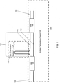
- FIG. 1 is an illustration of an athermal optical device according to an embodiment of the invention.
- Optical device 100 is shown to be an AMZI including input ports 102, output ports 104, and multi-mode interference (MMI) couplers 106 and 108.
- MMI multi-mode interference
- a waveguide propagation section is defined as the region between the input and output ports where there is more than one waveguide, and the waveguides have different delays/optical path lengths.
- the output port such as output ports 104
- light from different waveguides in the waveguide propagation section have undergone interference — for example with an MMI (such as MMIs 106 and 108) or a star coupler.
- waveguides 110 and 112 in the waveguide propagation section each have differing lengths, wherein waveguide 110 is longer than waveguide 112.
- the waveguide cross sections do not necessarily vary in the waveguide propagation section; however, other embodiments described below do utilize varying waveguide cross sections in both dimensions and thermo-optic coefficients (dn/dT).
- said waveguides are to be heated differently.
- the spectrum may be changed in a manner in which different waveguides would be heated separately in order to correct their individual phase errors (e.g., local fabrication errors).
- a single heater may be used to shift the spectrum to correct the deviation.
- a section of waveguide 110 is heated to fixed temperature T set which is greater than the ambient temperature of AMZI 100, T amb .
- the region of AMZI 100 subjected to the ambient temperature is shown as region 122.
- the length of the waveguide section included in heated region 120 is the difference in lengths between waveguide 110 and waveguide 112. In other words, the lengths of each waveguide which are affected by changes in T amb (shown as length 130) are equal, and the section of waveguide 110 included in heated region 120 does not experience any variations in optical path length with variations in T amb .
- the amplitude transmission characteristic of AMZI 100 is athermal and is thus not restricted to operate within a narrow temperature range as are prior art optical devices.
- region 120 of AMZI 100 represents a boundary line with low thermal conductivity.
- the effect of the design of AMZI 100 having heated region 120 is to improve power efficiency, increase temperature uniformity in the T set region, and minimize the heating of region 122.
- This may be achieved in a silicon-on-insulator (SOI) platform, for example, by etching a groove in the top silicon to remove a thermal conduction path between the T set region and T amb region. Additionally the substrates could be etched to remove thermal conduction paths.
- SOI silicon-on-insulator
- the outline of region 120 may represent the edge of a region of uniformly high thermal conductivity to improve the uniformity of the temperature in the T set region. This may be achieved by depositing a high thermal conductivity material above the top cladding (e.g., replace SiO 2 with diamond), by thinning the cladding or BOX and placing a conductor in close proximity to the waveguide, or by removing the substrate and depositing a high thermal conductivity material below the bottom cladding. In either of these implementations the high thermal conductivity material may connect directly to the waveguide layer using thermal shunts.
- a high thermal conductivity material above the top cladding e.g., replace SiO 2 with diamond
- the high thermal conductivity material may connect directly to the waveguide layer using thermal shunts.
- AMZI filter 100 (or a single stage thereof) contains a waveguide propagation section with more than one waveguide, and the waveguides are of different lengths.
- the waveguide propagation region is selectively heated, so that a given waveguide (i.e., waveguide 110) can be divided into a fraction that is at the ambient temperature (T amb ) and a fraction that is at the fixed temperature (T set ).
- the heated regions are chosen such that each waveguide has an equal length that is at temperature T amb , and any remaining length is at T set .
- each waveguide in response to a fluctuation in T amb , each waveguide has an identical change in the effective optical length, and the output frequency spectrum remains unchanged.
- the size of the heated region can be very small, making the technique power-efficient.
- varying T set may linearly shift the frequency spectrum of the filter. This property is useful both to intentionally modify the filter's frequency spectrum and to correct for deviations between the fabricated device and its pre-fabricated design.
- waveguides in the waveguide propagation section are referred to numerically as 1, 2 ... n, and the waveguide number is a variable 'w'.
- the waveguides' lengths are given by L(w).
- the effective index of the optical mode at position 'x' along a waveguide is n eft (w,x).
- the change in index with change in temperature (dn eff /dT) at position 'x' along a waveguide is dn dT w x .
- An athermal FIR filter may comprise waveguides that are subdivided into a fixed temperature (i.e., heated) region and an ambient region, as shown in FIG. 1 .
- L A (1) L A (2). Since the lengths of each waveguide in the waveguide propagation region at the ambient temperature are the same, when the ambient temperature changes, the optical path length of each waveguide changes the same amount, and the differences in length between the waveguides do not change. Therefore, an ambient temperature change may cause a slight time or phase delay in the overall transfer function of the filter but there is no change in the frequency spectrum of the transfer function.
- FIG. 2 is an illustration of an athermal optical device utilizing more than two waveguides according to an embodiment of the invention.
- FIR device 200 is illustrated as implementing an active technique to achieve athermicity in an FIR filter with more than two waveguides.
- Device 200 is shown to include two input ports 202 and two output ports 204.
- MMI 210 is coupled to said input ports to achieve mode transformation and interference.
- MMI 210 may be replaced by other interferometric components, such as one or more Y-junctions, one or more directional couplers, or a star coupler.
- a waveguide propagation section comprising waveguides 221-22n follows MMI 210, in which the different waveguides have different effective optical path lengths.
- MMI 212 follows said waveguide propagation section to achieve mode transformation and interference; output ports 204 follow MMI 212.
- MMI 212 could also be replaced with another interferometric component.
- one or more heaters 250 are used to heat part of the waveguide propagation region to a fixed temperature T set , shown as region 260.
- T set a fixed temperature
- the rest of said waveguide propagation section is subject to the surrounding ambient temperature.
- the cross section of the waveguide in the ambient region is constant, and as shown in this illustration, the length of the waveguide region at the ambient temperature is the same in each of the waveguides.
- heating element 250 comprises a single heating element used to heat each of waveguides 221-22n.
- This heating element may be, for example, a "snake-shaped" thin film resistor that runs along the length of several waveguides to be heated.
- Two potential locations of resistive thermal device (RTD) 252 for heat sensing are shown in this illustration. One location is between the traces of the thin film resistor (i.e., heating element 250). Another location is adjacent to the resistor but close enough that the temperature at the RTD is very close to the temperature of the resistor.
- RTD resistive thermal device
- the thermal gradient across device 200 at steady state is a function of T set and T amb .
- Embodiments of the invention further enable a linear shift in the spectrum of the transfer function of the filter by changing temperature T set .
- the teachings of this description are related to a single filter stage but could be applied to a filter with multiple stages.
- the mathematical analysis describes the response at a single output port to an input in a single input port, but can be extended to simultaneous inputs to different input ports.
- An FIR filter implemented in a PIC may be understood to split and/or interfere input modes from one or more input ports, propagate several modes through different time-delay paths in the waveguide propagation section, and then combine these modes through interference at one or more output ports.
- the input signal is split into waveguides numbered 1 through n, and the time delay to propagate through each waveguide is represented by d w .
- the complex amplitude corresponding to each waveguide is represented by c k,l,w .
- Representation of the filter's response as an impulse response function permits a description of the filter's transmission frequency spectrum. This is found by taking a Fourier transform of h k.l (t) , which will be written as H k,l ( ⁇ ). Representation of the transmission frequency spectrum in this way permits a mathematical description of how changing the heating profile of the waveguides changes the spectrum.
- the frequency spectrum after change in T set may be expressed in terms of H k,l ( ⁇ ) using the well-known Fourier transform properties, shown here for a function in time f(t) and its Fourier transform F( ⁇ ):
- the frequency spectrum of the transfer function after change in T set is: 1 s H k , l ⁇ s e j ⁇ t 0 1 ⁇ 1 s
- This function represents a scaling in the width of the entire frequency spectrum. Because the shift in center frequency is small compared to the carrier frequency, this spectral shift may typically be indistinguishable from a linear shift of the entire frequency spectrum, in the wavelength range of interest.
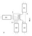
- FIG. 3 illustrates two optical devices sharing a common heated region according to an embodiment of the invention.
- device 300 includes MMI 302 and 304, coupled via waveguide propagation section 306;
- device 310 includes MMI 312 and 314, coupled via waveguides 316 and 318.
- sections of waveguide propagation section 306 are heated in a manner similar to the example embodiment of FIG. 2 (i.e., wherein the waveguides of waveguide propagation section 306 have variable section lengths to be heated, and equal section lengths subject to the ambient temperature).
- Waveguide 316 includes a portion to be heated to a constant temperature, similar to the embodiment of FIG. 1 .
- devices 300 and 310 both utilize region 350, which is heated to a constant temperature (i.e., greater than the ambient temperature).
- the heating of region 350 may be accomplished by using a single thin film electrode that covers the length of all of the waveguides within said region.
- said constant temperature region may be implemented with the use of regions of high and/or low thermal conductivity to make the temperature in the T set region uniform, thereby avoiding heating the T amb region and improving power efficiency. This implementation allows the heater, RTD, heater driver circuit, and feedback control circuit to be shared between two or more FIR filter devices or stages in an FIR filter.
- FIG. 4 is an illustration of an athermal device including a region of low thermal conductivity according to an embodiment of the invention.
- device 400 includes input port 402 and output port 404 coupled via waveguides 406.
- Device 400 utilizes heater 410 set at a fixed temperature to achieve athermal behavior.
- a region of low thermal conductivity, shown as region 412, is used to control the thermal gradient between heater 410 and the ambient region (i.e., the region outside of region 412).
- the low thermal conductivity of region 412 may be achieved, for example, by etching away the waveguide slab region between waveguides. Additionally a thermally conductive substrate may be removed in this region.
- the direction of the generated thermal gradient (shown in this example by directional arrow 414) corresponds to a change in temperature with distance that is roughly linear.
- a(w,x) is the fractional weight of the ambient temperature
- a waveguide may thus be described as being subdivided into effective lengths that are at the fixed and ambient temperatures, which may be different from the lengths which are and are not covered by a heating element:
- L A w ⁇ 0 L w a w x ⁇ d x
- L H w ⁇ 0 L w b w x ⁇ d x
- each waveguide that is heated to the heater temperature may change by a constant length between each adjacent waveguide, allowing the condition for athermicity to be satisfied.
- This embodiment demonstrates that not only can the shape of the heater or heated region be designed to heat different lengths of each waveguide in an FIR filter, but the thermal gradient can also be engineered so that the effective length of the heated region of each waveguide is correct to achieve athermal behavior.
- L A (k) L A (l) for any k and 1.
- This method embodiment works in the presence of a thermal gradient since the waveguide can be subdivided into an effective length at the ambient temperature and an effective length at the heated temperature, and because these effective lengths do not change as a function of the ambient and fixed temperatures.
- PICs may also utilize passively athermal FIR filters using waveguide regions with different effective thermo-optic coefficients dn/dT and heating a selected area of the PIC.
- passively athermal FIR filters using waveguide regions with different effective thermo-optic coefficients dn/dT and heating a selected area of the PIC.
- the frequency spectrum of the FIR filter linearly shifts, despite its athermicity, in the presence of global ambient temperature changes. Shifting the frequency spectrum can accomplish both active tuning of the filter characteristic and correction of deviations of the fabricated device from design. Using this technique, neither monitoring of temperatures on the chip nor feedback during heater operation is necessary.
- FIG. 5 is an illustration of an optical device for athermal operation and frequency spectrum tuning according to an embodiment of the invention.
- device 500 includes MMI 502 and MMI 504, coupled via waveguides 510 and 520; said waveguides comprise more than one value of dn/dT, either through differing materials or differing waveguide dimensions.
- a heater is used for active tuning, constant power dissipation may be used such that the heated region is raised to T amb +T off , where T off is a function of heater power dissipation. Measurement of temperatures on the chip may not necessary for this embodiment; said active tuning can be used to compensate for fabrication variations or to intentionally shift the spectrum of device 500.
- one of either waveguide sections 512 or 522 comprises a region having a differing dn/dT value, either through differing materials or differing waveguide dimensions, compared to the rest of waveguides 510 or 520, respectively.
- One of either waveguide sections 512 or 522 may also function as an active tuning section through the use of a heater.
- waveguide section 512 may comprise a region having a higher dn/dT value compared to the rest of waveguide 510 while waveguide section 522 comprises a heater, or vice-versa.
- waveguide section 512 may comprise a both a region having a higher dn/dT value compared to the rest of waveguide 510 and a heater either overlapping or in sequence with said waveguide section (e.g., said high dn/dT region and said heater are placed in series), while waveguide section 522 comprises a normal waveguide (i.e., a passive waveguide comprising the same dn/dT value as the "low" dn/dT region of waveguide 510), or vice-versa.
- a normal waveguide i.e., a passive waveguide comprising the same dn/dT value as the "low" dn/dT region of waveguide 510
- embodiments of the invention may further utilize passively athermal FIR filters having waveguide regions with different values of dn eff /dT in combination with heating a selected area of the device.
- Changing the power dissipated by the localized heater linearly shifts the frequency spectrum of the FIR filter, despite its athermal design (i.e., athermicity in the presence of global ambient temperature changes due to the varying dn eff /dT materials used). Shifting the frequency spectrum can accomplish both active tuning of the filter characteristic and correction of deviations of the fabricated device from design.
- the shift of the frequency spectrum is determined by the offset temperature, which may be set without the need for feedback, as it is proportional to the power dissipated in the heater. Since resistance of the heater does not vary strongly with temperature, the heater setpoint may be set with a constant current or constant voltage source. This technique may reduce power dissipation in comparison to the previously described embodiments, as heating is not required to achieve athermal operation but only to shift the frequency spectrum of the device. Some embodiments of the invention are further configured to heat a region within the high dn/dT waveguide cross section to maximize the energy efficiency of tuning.
- an FIR filter may use waveguide cross sections with differing effective thermo-optic coefficients (dn/dT).
- embodiments of the invention may further use a heater to heat a region of the waveguide propagation section for frequency spectrum tuning.
- the temperature of said heated region is T amb +T off .
- the thermal gradient in the vicinity of the heater may be described by b(w,x), where 0 ⁇ b ( w, x ) ⁇ 1.
- the equation may be satisfied by any combination of heaters — e.g., a single heater of any length on one of the two waveguides.
- the length of the heated region between adjacent waveguides may also have a constant linear increment.
- the heated region can therefore be wedge-shaped as shown in FIG 6A-6C and described in further detail below.
- This function represents a scaling in the width of the entire frequency spectrum.
- the shift in spectrum is entirely a function of the temperature offset from ambient and not a function of the ambient temperature, control of the transmission spectrum of the filter may be achieved without feedback.
- FIG. 6A ?? FIG. 6C are illustrations of athermal optical devices for frequency spectrum tuning according to embodiments of the invention. These embodiments describe PICs utilizing heating elements in combination with athermal FIR filters using waveguide regions with different values of dn eff /dT.
- FIG. 6A illustrates device 600 having input port 602 and output ports 604 coupled via plurality of waveguides 610.
- waveguides 610 are comprised two waveguide segment regions — low dn/dT region 612 and high dn/dT region 614, which is shown to include heated region 616.
- the waveguide segments of region 614 are also shown to be shorter in length than the waveguide segments of region 612.
- the shift of the frequency spectrum is determined by the offset temperature, which may be set without the need for feedback, since it is proportional to the power dissipated in the heater. Since resistance of the heater does not vary strongly with temperature, the heater setpoint may be set with a constant current or constant voltage source. This technique may reduce power dissipation in comparison to the previously described embodiments as heating is not required to achieve athermal operation but only to shift the frequency spectrum of the device. Heating a region within high dn/dT region 614 may also maximize the energy efficiency of tuning.
- thermo-optic coefficients (dn/dT) due to changes in the waveguide cross section
- the athermicity condition may be stated as the equality between the change in optical path lengths per unit change in temperature for different waveguides.
- FIG. 6A shows an AWG using regions with more than one waveguide cross section.
- the waveguide types may differ in refractive index n and in dn/dT.
- region 612 By using a region with a lower dn/dT for the majority of the waveguide propagation section (i.e., region 612), the total phase change along a waveguide with change in temperature is reduced.
- region 616 By using a region with higher dn/dT for the T set region (i.e., region 616), a smaller region needs to be heated to compensate for changes in T amb .
- the length that is to be heated is reduced by a factor of (dn/dT) high / (dn/dT) low compared to the length that would be heated if the entire device were made from the waveguide cross section with (dn/dT) low .
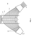
- FIG. 6B illustrates device 620 having input port 622 and output ports 624 coupled via plurality of waveguides 630.
- waveguides 630 are materials having different thermo-optic coefficients (dn/dT);; as shown in this illustration, a wedge-shaped region in the middle of device 620, shown as region 632, has a lower dn/dT value than the rest of the waveguide propagation region.
- the shape of region 632 is chosen to fulfill the condition for passive athermicity.
- a heater region 634 is disposed in or near the higher dn/dT region to improve the energy-efficiency of any desired spectral tuning.
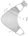
- FIG. 6C illustrates another variant of a passively athermal optical device with active tuning.
- Device 640 is shown as having input port 642 and output ports 644 coupled via plurality of waveguides 650.
- wedge-shaped region 652 includes segments of waveguides 650 that have a higher dn/dT value than the rest of the waveguide segments of propagation region 650.
- the heated region is coincident with high dn/dT wedge-shaped region 652 so the spectral tuning may be energy-efficient.
- the wedge shape is defined by the passive athermicity condition where the relative lengths of the waveguides with differing dn/dT are chosen to maintain a relative phase difference between adjacent waveguides with temperature fluctuation.
- the above described embodiments of the invention may comprise SOI or silicon based (e.g., silicon nitride (SiN)) devices, or may comprise devices formed from both silicon and a non-silicon material.
- Said non-silicon material (alternatively referred to as "heterogeneous material”) may comprise one of III-V material, magneto-optic material, or crystal substrate material.
- III-V semiconductors have elements that are found in group III and group V of the periodic table (e.g., Indium Gallium Arsenide Phosphide (InGaAsP), Gallium Indium Arsenide Nitride (GaInAsN)).
- the carrier dispersion effects of III-V based materials may be significantly higher than in silicon based materials, as electron speed in III-V semiconductors is much faster than that in silicon.
- III-V materials have a direct bandgap which enables efficient creation of light from electrical pumping.
- III-V semiconductor materials enable photonic operations with an increased efficiency over silicon for both generating light and modulating the refractive index of light.
- III-V semiconductor materials enable photonic operation with an increased efficiency at generating light from electricity and converting light back into electricity.
- the low optical loss and high quality oxides of silicon are thus combined with the electro-optic efficiency of III-V semiconductors in the heterogeneous optical devices described below; in embodiments of the invention, said heterogeneous devices utilize low loss heterogeneous optical waveguide transitions between the devices' heterogeneous and silicon-only waveguides.
- Magneto-optic materials allow heterogeneous PICs to operate based on the magneto-optic (MO) effect.
- Such devices may devices utilize the Faraday Effect, in which the magnetic field associated with an electrical signal modulates an optical beam, offering high bandwidth modulation, and rotates the electric field of the optical mode enabling optical isolators.
- Said magneto-optic materials may comprise, for example, materials such as such as iron, cobalt, or yttrium iron garnet (YIG).
- Crystal substrate materials provide heterogeneous PICs with a high electromechanical coupling linear electro optic coefficient, low transmission loss, and stable physical and chemical properties.
- Said crystal substrate materials may comprise, for example, lithium niobate (LiNbO3) or lithium tantalate (LiTaO3).
Abstract
Description
- Embodiments of the invention generally pertain to optical devices and more specifically to optical filters.
- Finite impulse response (FIR) filters are commonly implemented in photonic integrated circuits (PICs) to make devices such as asymmetric Mach-Zehnder interferometers (AMZIs), array waveguide gratings (AWGs), or wavelength division multiplexing (WDM) devices. FIR stages can also be assembled in series to make a more complex filter. FIR filter devices may be deployed in environments where there can be wide variations in ambient temperature, due to both environmental changes and the use of heat-dissipating components.
- FIR filters implemented in PICs have several technical problems. As the materials used to construct PICs have a temperature-dependent index of refraction, temperature changes to FIR filter devices can affect the spectral characteristics of the FIR filter. Correcting for this in a deployed PIC typically requires maintaining the device temperature within a narrow range; this maintenance may require energy-intensive heating of the entire PIC package.
- Furthermore, especially in the case of silicon-on-insulator (SOI) PICs, fabricated devices commonly have deviations from the design which lead to changes in the transmission spectrum. This is because SOI waveguides have a strong refractive index contrast between the silicon core and silicon dioxide cladding, and also because of the small dimensions typical of SOI waveguides; these small dimensions lead the effective index of a mode to be strongly dependent on changes in waveguide cross sectional dimensions. Fabrication deviations may be local, affecting different regions of a PIC to different degrees, or global, causing a constant deviation of the waveguide cross section from the design. Both local and global deviations detune the spectral response of an FIR filter.
- The following description includes discussion of figures having illustrations given by way of example of implementations of embodiments of the invention. The drawings should be understood by way of example, and not by way of limitation. As used herein, references to one or more "embodiments" are to be understood as describing a particular feature, structure, or characteristic included in at least one implementation of the invention. Thus, phrases such as "in one embodiment" or "in an alternate embodiment" appearing herein describe various embodiments and implementations of the invention, and do not necessarily all refer to the same embodiment. However, they are also not necessarily mutually exclusive.
-
FIG. 1 is an illustration of an athermal optical device according to an embodiment of the invention. -
FIG. 2 is an illustration of an athermal optical device utilizing more than two waveguides according to an embodiment of the invention. -
FIG. 3 illustrates two optical devices sharing a common heated region according to an embodiment of the invention. -
FIG. 4 is an illustration of an athermal device including a region of low thermal conductivity according to an embodiment of the invention. -
FIG. 5 is an illustration of an optical device for athermal operation and frequency spectrum tuning according to an embodiment of the invention. -
FIG. 6A - FIG. 6C are illustrations of athermal optical devices for frequency spectrum tuning according to embodiments of the invention. - Descriptions of certain details and implementations follow, including a description of the figures, which may depict some or all of the embodiments described below, as well as discussing other potential embodiments or implementations of the inventive concepts presented herein. An overview of embodiments of the invention is provided below, followed by a more detailed description with reference to the drawings.
- Embodiments of the invention describe systems, apparatuses and methods for providing athermicity and a tunable spectral response for optical filters. Finite impulse response (FIR) filters are commonly implemented in photonic integrated circuits (PICs) to make devices such as wavelength division multiplexing (WDM) devices, asymmetric Mach-Zehnder interferometers (AMZIs) and array waveguide gratings (AWGs). Athermicity of an FIR filter describes maintaining a consistent frequency transmission spectrum as the ambient temperature changes. A tunable spectral response for an FIR filter describes changing the spectrum of an FIR filter based on its application, as well as potentially correcting for fabrication deviations from the design. In addition, embodiments of the invention reduce energy dissipation requirements and control complexity compared to prior art solutions.
- In some embodiments of the invention, athermal operation of an FIR filter on a PIC is obtained via active control by heating a region of the filter. A control feedback loop maintains a set point (i.e., constant) temperature for the heated region; thus, there is no need to sense the ambient temperature or change the heated region's temperature as a function of the ambient temperature.
- By changing the set point temperature, the transmission spectrum of a filter may be linearly shifted to actively tune the filter's response. Shifting the transmission spectrum of a filter may also be used to correct for deviations of the fabricated device from the design. In the case of a global error in fabrication where all waveguides have a different effective index from what was designed, the fabricated device will have a linear spectral shift from the design intent, which embodiments of the invention can correct. Because only a fraction of the area of the device is to be selectively heated, this method of active control is power-efficient.
- Embodiments of the invention further describe design features for improving the power efficiency of a device. In some embodiments, the above described heated region is thermally isolated from the above described ambient region through modification of the thermal conduction path between the heated region and the ambient region, such as through localized thermal engineering of the substrate. In some embodiments, devices are designed to have waveguide regions having different thermo-optic coefficients (alternatively referred to herein as 'dn/dT,' as described below), either from differing materials or differing waveguide cross-sections, wherein a region where waveguides have a high dn/dT is heated, while the remaining bulk of the FIR device uses waveguides with a low dn/dT. Control at the PIC scale can be further simplified if an actively heated region is shared by two or more FIR filter devices.
- Throughout this specification, several terms of art are used. These terms are to take on their ordinary meaning in the art from which they come, unless specifically defined herein or the context of their use would clearly suggest otherwise. In the following description numerous specific details are set forth to provide a thorough understanding of the embodiments. One skilled in the relevant art will recognize, however, that the techniques described herein can be practiced without one or more of the specific details, or with other methods, components, materials, etc. In other instances, well-known structures, materials, or operations are not shown or described in detail to avoid obscuring certain aspects.
-
FIG. 1 is an illustration of an athermal optical device according to an embodiment of the invention.Optical device 100 is shown to be an AMZI includinginput ports 102,output ports 104, and multi-mode interference (MMI)couplers MMIs 106 and 108) or a star coupler. - In this example,
waveguides waveguide 110 is longer thanwaveguide 112. In this example embodiment, the waveguide cross sections do not necessarily vary in the waveguide propagation section; however, other embodiments described below do utilize varying waveguide cross sections in both dimensions and thermo-optic coefficients (dn/dT). In embodiments where different waveguides in the waveguide propagation section have different deviations in the cross section, said waveguides are to be heated differently. For example, in embodiments having three or more waveguides in the waveguide propagation section, the spectrum may be changed in a manner in which different waveguides would be heated separately in order to correct their individual phase errors (e.g., local fabrication errors). In embodiments with only two waveguides in the waveguide propagation section having different deviations in the cross section, a single heater may be used to shift the spectrum to correct the deviation. - In this embodiment, a section of
waveguide 110, shown to be included inregion 120, is heated to fixed temperature Tset which is greater than the ambient temperature of AMZI 100, Tamb. The region of AMZI 100 subjected to the ambient temperature is shown asregion 122. The length of the waveguide section included inheated region 120 is the difference in lengths betweenwaveguide 110 andwaveguide 112. In other words, the lengths of each waveguide which are affected by changes in Tamb (shown as length 130) are equal, and the section ofwaveguide 110 included inheated region 120 does not experience any variations in optical path length with variations in Tamb . Because the relative phase of modes in different waveguides at the outputs of the waveguide propagation section does not change with changes to Tamb, the amplitude transmission characteristic ofAMZI 100 is athermal and is thus not restricted to operate within a narrow temperature range as are prior art optical devices. - In one embodiment,
region 120 of AMZI 100 represents a boundary line with low thermal conductivity. The effect of the design of AMZI 100 having heatedregion 120 is to improve power efficiency, increase temperature uniformity in the Tset region, and minimize the heating ofregion 122. This may be achieved in a silicon-on-insulator (SOI) platform, for example, by etching a groove in the top silicon to remove a thermal conduction path between the Tset region and Tamb region. Additionally the substrates could be etched to remove thermal conduction paths. - In another embodiment, the outline of region 120 (i.e., the Tset region) may represent the edge of a region of uniformly high thermal conductivity to improve the uniformity of the temperature in the Tset region. This may be achieved by depositing a high thermal conductivity material above the top cladding (e.g., replace SiO2 with diamond), by thinning the cladding or BOX and placing a conductor in close proximity to the waveguide, or by removing the substrate and depositing a high thermal conductivity material below the bottom cladding. In either of these implementations the high thermal conductivity material may connect directly to the waveguide layer using thermal shunts.
- Thus, in this embodiment, athermal operation of an FIR filter in a PIC is accomplished by heating a selected area of the filter to a fixed temperature. AMZI filter 100 (or a single stage thereof) contains a waveguide propagation section with more than one waveguide, and the waveguides are of different lengths. The waveguide propagation region is selectively heated, so that a given waveguide (i.e., waveguide 110) can be divided into a fraction that is at the ambient temperature (Tamb) and a fraction that is at the fixed temperature (Tset). The heated regions are chosen such that each waveguide has an equal length that is at temperature Tamb, and any remaining length is at Tset. The result is that in response to a fluctuation in Tamb, each waveguide has an identical change in the effective optical length, and the output frequency spectrum remains unchanged. The size of the heated region can be very small, making the technique power-efficient. Furthermore, as described in more detail below, varying Tset may linearly shift the frequency spectrum of the filter. This property is useful both to intentionally modify the filter's frequency spectrum and to correct for deviations between the fabricated device and its pre-fabricated design.
- The following description teaches operation of a single stage of an FIR device. It is to be understood that the same explanation also applies to a filter of multiple stages, such as an interleaver containing several cascaded AMZIs. For this description, waveguides in the waveguide propagation section are referred to numerically as 1, 2 ... n, and the waveguide number is a variable 'w'. The waveguides' lengths are given by L(w). The effective index of the optical mode at position 'x' along a waveguide is neft(w,x). The change in index with change in temperature (dneff/dT) at position 'x' along a waveguide is

- An athermal FIR filter may comprise waveguides that are subdivided into a fixed temperature (i.e., heated) region and an ambient region, as shown in
FIG. 1 . The fixed temperature region may be hotter than the maximum ambient temperature to ensure device reliability over its operating temperature range. It is assumed for the following explanation that the waveguides all have the same cross section, both in dimensions and materials, such that:
- Under these conditions, the heated and ambient regions' lengths sum to equal the total length of the waveguide is:

- For an AMZI including two waveguides (such as AMZI 100) the heated region's length is chosen such that, L(1) - L(2) = LH(1) - LH(2). If waveguide 1 is longer than waveguide 2, then the length of waveguide 1 that is heated may be equal to the difference in lengths, and waveguide 2 may be completely ambient (e.g.,
waveguide 112 shown inFIG. 1 ). - From the previous equation it follows that LA(1) = LA(2). Since the lengths of each waveguide in the waveguide propagation region at the ambient temperature are the same, when the ambient temperature changes, the optical path length of each waveguide changes the same amount, and the differences in length between the waveguides do not change. Therefore, an ambient temperature change may cause a slight time or phase delay in the overall transfer function of the filter but there is no change in the frequency spectrum of the transfer function.
- To extend this result to filters with more than two waveguides such as AWGs, fixed temperature lengths LH(w) are chosen such that LA(n) = LA(l) for any n and 1.
FIG. 2 is an illustration of an athermal optical device utilizing more than two waveguides according to an embodiment of the invention. - In this embodiment,
FIR device 200 is illustrated as implementing an active technique to achieve athermicity in an FIR filter with more than two waveguides.Device 200 is shown to include twoinput ports 202 and twooutput ports 204.MMI 210 is coupled to said input ports to achieve mode transformation and interference. In other embodiments,MMI 210 may be replaced by other interferometric components, such as one or more Y-junctions, one or more directional couplers, or a star coupler. - A waveguide propagation section comprising waveguides 221-22n follows
MMI 210, in which the different waveguides have different effective optical path lengths.MMI 212 follows said waveguide propagation section to achieve mode transformation and interference;output ports 204 followMMI 212. In other embodiments,MMI 212 could also be replaced with another interferometric component. - In this embodiment, within said waveguide propagation section, one or
more heaters 250 are used to heat part of the waveguide propagation region to a fixed temperature Tset, shown asregion 260. The rest of said waveguide propagation section is subject to the surrounding ambient temperature. The cross section of the waveguide in the ambient region is constant, and as shown in this illustration, the length of the waveguide region at the ambient temperature is the same in each of the waveguides. - In this embodiment,
heating element 250 comprises a single heating element used to heat each of waveguides 221-22n. This heating element may be, for example, a "snake-shaped" thin film resistor that runs along the length of several waveguides to be heated. Two potential locations of resistive thermal device (RTD) 252 for heat sensing are shown in this illustration. One location is between the traces of the thin film resistor (i.e., heating element 250). Another location is adjacent to the resistor but close enough that the temperature at the RTD is very close to the temperature of the resistor. Other configurations for both the heater and RTD can be used in other embodiments of the invention. - It is to be understood that the thermal gradient across
device 200 at steady state is a function of Tset and Tamb. At steady state, provided Tset > Tamb, the temperature at any location in the device may be described as a linear combination of Tamb and Tset, satisfying the equation T=a∗Tamb + b∗Tset, where a+b = 1; there is not variation of the spatial distribution of thermal contours with changes in Tset or Tamb. - Embodiments of the invention further enable a linear shift in the spectrum of the transfer function of the filter by changing temperature Tset. The teachings of this description are related to a single filter stage but could be applied to a filter with multiple stages. In addition, the mathematical analysis describes the response at a single output port to an input in a single input port, but can be extended to simultaneous inputs to different input ports.
- An FIR filter implemented in a PIC may be understood to split and/or interfere input modes from one or more input ports, propagate several modes through different time-delay paths in the waveguide propagation section, and then combine these modes through interference at one or more output ports. The transfer function may be described with an impulse response function. This is the response of the system to an input which is a narrow pulse at time t=0, represented as a delta function, δ(t-0). The impulse response function of the filter for input port k and output port 1 is:

- The input signal is split into waveguides numbered 1 through n, and the time delay to propagate through each waveguide is represented by dw. When light in different waveguides are combined through interference at the output, the complex amplitude corresponding to each waveguide is represented by ck,l,w. Representation of the filter's response as an impulse response function permits a description of the filter's transmission frequency spectrum. This is found by taking a Fourier transform of hk.l(t) , which will be written as Hk,l (ω). Representation of the transmission frequency spectrum in this way permits a mathematical description of how changing the heating profile of the waveguides changes the spectrum.
- The delay times dw are proportional to the effective path lengths of the waveguides. Since the effective ambient length of each waveguide is the same and the effective heated length of each waveguide is different, if the fixed temperature Tset is changed, the new delay time (gw) changes by an amount proportional to the total path delay minus a constant delay time, d0, which is identical for each waveguide and corresponds to the unheated ambient length of each path. Mathematically this may be described by the following equation where the factor s equals 1 when there is no change in Tset, but has a different value when temperature is changed:

- The frequency spectrum after change in Tset may be expressed in terms of Hk,l (ω) using the well-known Fourier transform properties, shown here for a function in time f(t) and its Fourier transform F(ω):
- Time shift property: f(t-t0) corresponds to F(ω)e―jωt
0 - Scaling property for real a: f(a∗t) corresponds to

- Applying these properties, the frequency spectrum of the transfer function after change in Tset is:

- The amplitude of this function is:

- This function represents a scaling in the width of the entire frequency spectrum. Because the shift in center frequency is small compared to the carrier frequency, this spectral shift may typically be indistinguishable from a linear shift of the entire frequency spectrum, in the wavelength range of interest.
-
FIG. 3 illustrates two optical devices sharing a common heated region according to an embodiment of the invention. In this embodiment,device 300 includesMMI waveguide propagation section 306;device 310 includesMMI waveguides - In this embodiment, sections of
waveguide propagation section 306 are heated in a manner similar to the example embodiment ofFIG. 2 (i.e., wherein the waveguides ofwaveguide propagation section 306 have variable section lengths to be heated, and equal section lengths subject to the ambient temperature).Waveguide 316 includes a portion to be heated to a constant temperature, similar to the embodiment ofFIG. 1 . As shown in this illustration,devices region 350, which is heated to a constant temperature (i.e., greater than the ambient temperature). - The heating of
region 350 may be accomplished by using a single thin film electrode that covers the length of all of the waveguides within said region. In other embodiments, said constant temperature region may be implemented with the use of regions of high and/or low thermal conductivity to make the temperature in the Tset region uniform, thereby avoiding heating the Tamb region and improving power efficiency. This implementation allows the heater, RTD, heater driver circuit, and feedback control circuit to be shared between two or more FIR filter devices or stages in an FIR filter. -
FIG. 4 is an illustration of an athermal device including a region of low thermal conductivity according to an embodiment of the invention. In this embodiment,device 400 includesinput port 402 andoutput port 404 coupled viawaveguides 406.Device 400 utilizesheater 410 set at a fixed temperature to achieve athermal behavior. A region of low thermal conductivity, shown asregion 412, is used to control the thermal gradient betweenheater 410 and the ambient region (i.e., the region outside of region 412). - The low thermal conductivity of
region 412 may be achieved, for example, by etching away the waveguide slab region between waveguides. Additionally a thermally conductive substrate may be removed in this region. The direction of the generated thermal gradient (shown in this example by directional arrow 414) corresponds to a change in temperature with distance that is roughly linear. - The following description teaches the athermicity condition more generally where there is a thermal gradient in the vicinity of the heater, but the waveguides still have an invariant cross section. Assuming the thermal gradients are solely due to interaction of two thermal bodies — a heat sink held at the ambient temperature and the heater, and further assuming the temperature has reached steady state, the temperature at any location in the device may be described as a linear combination of the ambient and the fixed temperature. Temperature at a location along a waveguide may be expressed as:

- a(w,x) is the fractional weight of the ambient temperature, and b(w,x) is the fractional weight of the set temperature. Both of these functions are temperature-invariant: They do not change as Tamb or Tset change. At all locations, a(w,x) + b(w,x) = 1.
- A waveguide may thus be described as being subdivided into effective lengths that are at the fixed and ambient temperatures, which may be different from the lengths which are and are not covered by a heating element:

- Therefore the effective length of each waveguide that is heated to the heater temperature may change by a constant length between each adjacent waveguide, allowing the condition for athermicity to be satisfied. This embodiment demonstrates that not only can the shape of the heater or heated region be designed to heat different lengths of each waveguide in an FIR filter, but the thermal gradient can also be engineered so that the effective length of the heated region of each waveguide is correct to achieve athermal behavior.
- The condition to be satisfied for athermicity in this case is also: LA(k) = LA(l) for any k and 1. This method embodiment works in the presence of a thermal gradient since the waveguide can be subdivided into an effective length at the ambient temperature and an effective length at the heated temperature, and because these effective lengths do not change as a function of the ambient and fixed temperatures.
- PICs according to embodiments of the invention, may also utilize passively athermal FIR filters using waveguide regions with different effective thermo-optic coefficients dn/dT and heating a selected area of the PIC. By changing the power dissipated by the localized heater, the frequency spectrum of the FIR filter linearly shifts, despite its athermicity, in the presence of global ambient temperature changes. Shifting the frequency spectrum can accomplish both active tuning of the filter characteristic and correction of deviations of the fabricated device from design. Using this technique, neither monitoring of temperatures on the chip nor feedback during heater operation is necessary.
-
FIG. 5 is an illustration of an optical device for athermal operation and frequency spectrum tuning according to an embodiment of the invention. In this embodiment,device 500 includesMMI 502 andMMI 504, coupled viawaveguides device 500. - In this embodiment, one of either
waveguide sections waveguides waveguide sections waveguide section 512 may comprise a region having a higher dn/dT value compared to the rest ofwaveguide 510 whilewaveguide section 522 comprises a heater, or vice-versa. In other embodiments,waveguide section 512 may comprise a both a region having a higher dn/dT value compared to the rest ofwaveguide 510 and a heater either overlapping or in sequence with said waveguide section (e.g., said high dn/dT region and said heater are placed in series), whilewaveguide section 522 comprises a normal waveguide (i.e., a passive waveguide comprising the same dn/dT value as the "low" dn/dT region of waveguide 510), or vice-versa. - Thus, embodiments of the invention may further utilize passively athermal FIR filters having waveguide regions with different values of dneff/dT in combination with heating a selected area of the device. Changing the power dissipated by the localized heater linearly shifts the frequency spectrum of the FIR filter, despite its athermal design (i.e., athermicity in the presence of global ambient temperature changes due to the varying dneff/dT materials used). Shifting the frequency spectrum can accomplish both active tuning of the filter characteristic and correction of deviations of the fabricated device from design. Using this technique, neither monitoring of temperatures on the chip nor feedback during heater operation is necessary: the heated region's temperature is a sum of the ambient temperature and an offset temperature that is a linear function of power dissipated by the heater:

- The shift of the frequency spectrum is determined by the offset temperature, which may be set without the need for feedback, as it is proportional to the power dissipated in the heater. Since resistance of the heater does not vary strongly with temperature, the heater setpoint may be set with a constant current or constant voltage source. This technique may reduce power dissipation in comparison to the previously described embodiments, as heating is not required to achieve athermal operation but only to shift the frequency spectrum of the device. Some embodiments of the invention are further configured to heat a region within the high dn/dT waveguide cross section to maximize the energy efficiency of tuning.
- For passive athermal operation, an FIR filter may use waveguide cross sections with differing effective thermo-optic coefficients (dn/dT). Each waveguide's length L(w) may be subdivided into lengths with the two different values of dn/dT:

- The net change in optical length with temperature is the same for all waveguides:

- The result is analogous to the effect of the previously described embodiments utilizing a heater to heat a portion of an optical device to a fixed temperature — when the ambient temperature is changed, the effective optical path length of each waveguide is changed by a fixed amount. The differences in effective optical path lengths between different waveguides are invariant with temperature. A change is ambient temperature may therefore result in a small time/phase delay, but no change in the transmission frequency spectrum.
- This relation may also be stated in integral form, which is applicable for embodiments with free variation of dn/dT along the waveguides' length instead of two discrete cross sections:

- Using the above described passive athermal design, embodiments of the invention may further use a heater to heat a region of the waveguide propagation section for frequency spectrum tuning. The temperature of said heated region is Tamb+Toff. The thermal gradient in the vicinity of the heater may be described by b(w,x), where 0 ≤ b(w, x) ≤ 1. The temperature at any point along a waveguide may be described by:

- The shape of the heated region may chosen such that:

- For an optical device with two waveguides in its waveguide propagation section, the equation may be satisfied by any combination of heaters — e.g., a single heater of any length on one of the two waveguides. For an optical device where the effective length difference in adjacent waveguides has a constant linear increment, the length of the heated region between adjacent waveguides may also have a constant linear increment. The heated region can therefore be wedge-shaped as shown in
FIG 6A-6C and described in further detail below. - When the offset temperature is changed, the relative changes in path lengths causes a linear shift in the transmission frequency spectrum of the FIR filter, as explained by the following equations.
- The delay time of a waveguide when Toff=0 expressed in terms of the speed of light, c, is:

- When the heater is used the delay time changes to:


- The following variable substitutions may be made:


- Now the equation for d(w,Toff) matches the form of the equation for waveguide delay with temperature shift from the previous section, gw = s * (dw - d 0) + d 0 . Therefore, using the math in the previous section, if the unheated frequency spectrum of the transfer function is from input port k to output port 1 is:

- Once the heater temperature is heated to an offset from the ambient temperature of Toff, the magnitude of the frequency spectrum is:

- This function represents a scaling in the width of the entire frequency spectrum. As the shift in spectrum is entirely a function of the temperature offset from ambient and not a function of the ambient temperature, control of the transmission spectrum of the filter may be achieved without feedback.
-
FIG. 6A ―FIG. 6C are illustrations of athermal optical devices for frequency spectrum tuning according to embodiments of the invention. These embodiments describe PICs utilizing heating elements in combination with athermal FIR filters using waveguide regions with different values of dneff/dT.FIG. 6A illustratesdevice 600 havinginput port 602 andoutput ports 604 coupled via plurality ofwaveguides 610. In this embodiment,waveguides 610 are comprised two waveguide segment regions — low dn/dT region 612 and high dn/dT region 614, which is shown to includeheated region 616. The waveguide segments ofregion 614 are also shown to be shorter in length than the waveguide segments ofregion 612. - Said heated region's temperature is the sum of the ambient temperature and an offset temperature that is a linear function of power dissipated by the heater: Theated=Tamb+Toff. The shift of the frequency spectrum is determined by the offset temperature, which may be set without the need for feedback, since it is proportional to the power dissipated in the heater. Since resistance of the heater does not vary strongly with temperature, the heater setpoint may be set with a constant current or constant voltage source. This technique may reduce power dissipation in comparison to the previously described embodiments as heating is not required to achieve athermal operation but only to shift the frequency spectrum of the device. Heating a region within high dn/
dT region 614 may also maximize the energy efficiency of tuning. - For embodiments of the invention having thermo-optic coefficients (dn/dT) due to changes in the waveguide cross section, the athermicity condition may be stated as the equality between the change in optical path lengths per unit change in temperature for different waveguides. The change in optical path length of a waveguide per change in ambient temperature may be expressed as:

- The condition to be satisfied is D(k) = D(l) for any k and 1. The implication of the equation is that for a change in ambient temperature dT, the change in optical path length in each path in the waveguide propagation region is the same. This is analogous to the previous equation LA(1) = LA(2), except that this more general description allows for variations in both neff and dn/dT, and also allows for a design with arbitrary thermal gradients between the heated and ambient region expressed by a(w,x).
- Thus embodiments of the invention include optical devices that utilize multiple dn/dT regions to decrease the power required to heat the above described Tset region.
FIG. 6A shows an AWG using regions with more than one waveguide cross section. The waveguide types may differ in refractive index n and in dn/dT. By using a region with a lower dn/dT for the majority of the waveguide propagation section (i.e., region 612), the total phase change along a waveguide with change in temperature is reduced. By using a region with higher dn/dT for the Tset region (i.e., region 616), a smaller region needs to be heated to compensate for changes in Tamb. The length that is to be heated is reduced by a factor of (dn/dT)high / (dn/dT)low compared to the length that would be heated if the entire device were made from the waveguide cross section with (dn/dT)low. -
FIG. 6B illustratesdevice 620 havinginput port 622 andoutput ports 624 coupled via plurality ofwaveguides 630. In this embodiment,waveguides 630 are materials having different thermo-optic coefficients (dn/dT);; as shown in this illustration, a wedge-shaped region in the middle ofdevice 620, shown asregion 632, has a lower dn/dT value than the rest of the waveguide propagation region. The shape ofregion 632 is chosen to fulfill the condition for passive athermicity. Thus, the design ofregion 632 provides athermicity todevice 620. In this embodiment, a heater (region 634) is disposed in or near the higher dn/dT region to improve the energy-efficiency of any desired spectral tuning. -
FIG. 6C illustrates another variant of a passively athermal optical device with active tuning.Device 640 is shown as havinginput port 642 andoutput ports 644 coupled via plurality ofwaveguides 650. In this embodiment, wedge-shapedregion 652 includes segments ofwaveguides 650 that have a higher dn/dT value than the rest of the waveguide segments ofpropagation region 650. In this embodiment, the heated region is coincident with high dn/dT wedge-shapedregion 652 so the spectral tuning may be energy-efficient. The wedge shape is defined by the passive athermicity condition where the relative lengths of the waveguides with differing dn/dT are chosen to maintain a relative phase difference between adjacent waveguides with temperature fluctuation. - Reference throughout the foregoing specification to "one embodiment" or "an embodiment" means that a particular feature, structure or characteristic described in connection with the embodiment is included in at least one embodiment of the present invention. Thus, appearances of the phrases "in one embodiment" or "in an embodiment" in various places throughout the specification are not necessarily all referring to the same embodiment. Furthermore, the particular features, structures or characteristics may be combined in any suitable manner in one or more embodiments. In addition, it is appreciated that the figures provided are for explanation purposes to persons ordinarily skilled in the art and that the drawings are not necessarily drawn to scale. It is to be understood that the various regions, layers and structures of figures may vary in size and dimensions.
- The above described embodiments of the invention may comprise SOI or silicon based (e.g., silicon nitride (SiN)) devices, or may comprise devices formed from both silicon and a non-silicon material. Said non-silicon material (alternatively referred to as "heterogeneous material") may comprise one of III-V material, magneto-optic material, or crystal substrate material.
- III-V semiconductors have elements that are found in group III and group V of the periodic table (e.g., Indium Gallium Arsenide Phosphide (InGaAsP), Gallium Indium Arsenide Nitride (GaInAsN)). The carrier dispersion effects of III-V based materials may be significantly higher than in silicon based materials, as electron speed in III-V semiconductors is much faster than that in silicon. In addition, III-V materials have a direct bandgap which enables efficient creation of light from electrical pumping. Thus, III-V semiconductor materials enable photonic operations with an increased efficiency over silicon for both generating light and modulating the refractive index of light.
- Thus, III-V semiconductor materials enable photonic operation with an increased efficiency at generating light from electricity and converting light back into electricity. The low optical loss and high quality oxides of silicon are thus combined with the electro-optic efficiency of III-V semiconductors in the heterogeneous optical devices described below; in embodiments of the invention, said heterogeneous devices utilize low loss heterogeneous optical waveguide transitions between the devices' heterogeneous and silicon-only waveguides.
- Magneto-optic materials allow heterogeneous PICs to operate based on the magneto-optic (MO) effect. Such devices may devices utilize the Faraday Effect, in which the magnetic field associated with an electrical signal modulates an optical beam, offering high bandwidth modulation, and rotates the electric field of the optical mode enabling optical isolators. Said magneto-optic materials may comprise, for example, materials such as such as iron, cobalt, or yttrium iron garnet (YIG).
- Crystal substrate materials provide heterogeneous PICs with a high electromechanical coupling linear electro optic coefficient, low transmission loss, and stable physical and chemical properties. Said crystal substrate materials may comprise, for example, lithium niobate (LiNbO3) or lithium tantalate (LiTaO3).
- In the foregoing detailed description, the method and apparatus of the present invention have been described with reference to specific exemplary embodiments thereof. It will, however, be evident that various modifications and changes may be made thereto without departing from the broader spirit and scope of the present invention. The present specification and figures are accordingly to be regarded as illustrative rather than restrictive.
-
- 1. An optical device comprising:
- an input port;
- an output port;
- a plurality of waveguides coupled to the input port and the output port, the plurality of. waveguides comprising at least one optical waveguide having a first and a second waveguide section, wherein the first waveguide section has an optical wavelength response as a function of an ambient temperature of the optical device;
- at least one heating element to heat the second waveguide sections of the plurality of waveguides;
- a temperature sensor to measure the temperature of the second waveguide section; and
- a temperature controller to control the heating element(s) based, at least in part, on the temperature sensor so that the temperature of the second waveguide section is fixed and greater than the ambient temperature of the optical device.
- 2. The optical device of clause 1, wherein the plurality of waveguides coupled to the input port and the output port further comprises:
a second optical waveguide comprising a third and a fourth waveguide section; wherein the third waveguide section has an optical wavelength response as a function of the ambient temperature of the optical device, the heating element(s) to heat both the second and the fourth waveguide section, and the temperature controller to control the heating element(s) so that the temperature of the second and the fourth waveguide section is fixed and greater than the ambient temperature of the optical device. - 3. The optical device of clause 2, wherein the first and third waveguide sections comprise the same length.
- 4. The optical device of clause 2, wherein the length the fourth waveguide section differs from the length of the second waveguide section.
- 5. The optical device of clause 2, wherein the heating element(s) consists of a single heating electrode disposed near both of the second and fourth waveguide sections.
- 6. The optical device of clause 2, wherein the heating element(s) comprises a first and a second heating electrode, the first heating electrode disposed near the second waveguide section, the second heating electrode disposed near the fourth waveguide section, and the temperature controller to independently control each of the first and the second heating electrodes.
- 7. The optical device of clause 1, wherein the temperature controller receives control signals to adjust the fixed temperature to change at least one of the frequency of transmission or the filter spectrum of the optical device.
- 8. The optical device of clause 1, further comprising a moat having a low thermal conductivity and positioned around the heating element.
- 9. The optical device of clause 1, wherein the first and second waveguide sections each have a different temperature coefficient of refractive index (dnldT).
- 10. The optical device of clause 9, wherein the material of the second waveguide section comprises a higher temperature coefficient of refractive index (dnldT) than the material of the first waveguide section.
- 11. The optical device of clause 1, wherein the plurality of waveguides includes another waveguide having a section comprising a material having a higher temperature coefficient of refractive index (dnldT) than the material of at least one waveguide having the first and second waveguide sections.
- 12. The optical device of clause 1, wherein the optical device comprises one of a WDM device, an AMZI, an interleaver, an AWG, a combination of an FIR and infinite impulse response (IIR) filter.
- 13. A substrate including a plurality of optical devices, comprising:
- a first optical device comprising:
- an input port;
- an output port; and
- a plurality of waveguides coupled to the input port and the output port, the plurality of waveguides comprising at least one optical waveguide having a first and a second waveguide section, wherein the first waveguide section has an optical wavelength response as a function of an ambient temperature of the system;
- a second optical device comprising:
- an input port;
- an output port; and
- a plurality of waveguides coupled to the input port and the output port, the plurality of waveguides comprising at least one optical waveguide having a third and a fourth waveguide section, wherein the third waveguide section has an optical wavelength response as a function of an ambient temperature of the system;
- a region including the second waveguide section of the first optical device and the fourth waveguide section of the second optical device;
- a heating element to heat the region;
- a temperature sensor to measure the temperature of the region; and
- a temperature controller to control the heating element based, at least in part, on the temperature sensor so that the temperature of the region is fixed and greater than the ambient temperature of the system.
- a first optical device comprising:
- 14. An apparatus comprising:
- a passively athermal optical device including:
- an input port;
- an output port;
- a plurality of waveguides coupled to the input port and the output port,
- wherein each of the plurality of waveguides comprises:
- a first waveguide section; and
- a second waveguide section having a higher temperature coefficient of refractive index (dn/dT) than the first section;
- a heating element to heat at least a portion of the second waveguide sections of the plurality of waveguides; and
- a temperature controller to control the heating element to adjust a frequency spectrum of the optical device.
- a passively athermal optical device including:
- 15. the apparatus of clause 14, wherein a material of the second waveguide section comprises a higher temperature coefficient of refractive index (dn/dT) than a material of the first waveguide section.
-
- 16. A tunable optical filter, comprising:
- a first waveguide including a first waveguide section and a second waveguide section, the second waveguide section having a higher temperature coefficient of refractive index than the first waveguide section;
- a second waveguide;
- an input coupler to split incident light into the first and second waveguides;
- an output coupler to interfere light from the first and second waveguides to produce interfered light;
- a heater to heat at least a portion of the second waveguide section; and
- a temperature controller to control the heater to tune a frequency of the interfered light.
- 17. The tunable optical filter of clause 16, wherein the temperature coefficient of refractive index represents a change in refractive index with respect to temperature.
- 18. The tunable optical filter of clause 16 or clause 17, wherein:
- a material of the first waveguide section includes a first material having a first thermal conductivity; and
- a material of the second waveguide section includes a second material having a second thermal conductivity greater than the first thermal conductivity.
- 19. The tunable optical filter of any of clauses 16-18, wherein a width of the second waveguide section is greater than a width of the first waveguide section.
- 20. The tunable optical filter of any of clauses 13-19, wherein the temperature controller is configured to tune the frequency at least in part in response to an amount of power dissipated by the heater.
- 21. The tunable optical filter of any of clauses 16-20, further comprising a temperature sensor configured to sense a temperature of the portion of the second waveguide section, and
wherein the temperature controller is configured to tune the frequency at least in part in response to the sensed temperature. - 22. The tunable optical filter of any of clauses 16-21, wherein:
- the first waveguide section has a first length; and
- the second waveguide section has a second length greater than the first length.
- 23. The tunable optical filter of any of clauses 16-21, wherein:
- the first waveguide section has a first length; and
- the second waveguide section has a second length less than the first length.
- 24. The tunable optical filter of any of clauses 16-23, wherein:
- the first waveguide section has a first length and a first temperature coefficient of refractive index;
- the second waveguide section has a second length and a second temperature coefficient of refractive index greater than the first temperature coefficient of refractive index;
- the second waveguide includes a third waveguide section and a fourth waveguide section;
- the third waveguide section has a third length and a third temperature coefficient of refractive index;
- the fourth waveguide section has a fourth length and a fourth temperature coefficient of refractive index greater than the third temperature coefficient of refractive index; and
- a product of the first length and the first temperature coefficient of refractive index added to a product of the second length and the second temperature coefficient of refractive index differs from a product of the third length and the third temperature coefficient of refractive index added to a product of the fourth length and the fourth temperature coefficient of refractive index.
- 25. A method for tuning a tunable optical filter, the method comprising:
- splitting incident light into first and second waveguides, the first waveguide including a first waveguide section and a second waveguide section, the second waveguide section having a higher temperature coefficient of refractive index than the first waveguide section;
- interfering light from the first and second waveguides to produce interfered light;
- heating at least a portion of the second waveguide section with a heater; and
- controlling the heater with a temperature controller to tune a frequency of the interfered light.
- 26. The method of clause 25, wherein:
- a material of the first waveguide section includes a first material having a first thermal conductivity; and
- a material of the second waveguide section includes a second material having a second thermal conductivity greater than the first thermal conductivity.
- 27. The method of clause 25 or clause 26, wherein a width of the second waveguide section is greater than a width of the first waveguide section.
- 28. The method of any of clauses 25-27, wherein the temperature controller is configured to tune the frequency at least in part in response to an amount of power dissipated by the heater.
- 29. The method of any of clauses 25-28, further comprising a temperature sensor configured to sense a temperature of the portion of the second waveguide section, and
wherein the temperature controller is configured to tune the frequency at least in part in response to the sensed temperature. - 30. The method of any of clauses 25-29, wherein:
- the first waveguide section has a first length; and
- the second waveguide section has a second length different from the first length.
Claims (15)
- A semiconductor interferometer filter (100), comprising:an input coupler (106) to receive incident light and produce split light comprising multiple beams;an output coupler (108) to combine the multiple beams to produce interfered light;a first waveguide (112) that couples one of the multiple beams from the input coupler to the output coupler, the first waveguide having a length (130);a second waveguide (110) that couples another of the multiple beams from the input coupler to the output coupler, the second waveguide having an elongated length that is longer than the length of the first waveguide due to a delay path section of the second waveguide; anda heater to heat the delay path section to a higher temperature (120) than an ambient temperature (122) of the first waveguide and a remaining portion of the second waveguide that is not in the delay path section of the second waveguide.
- The semiconductor interferometer filter of claim 1, wherein the path delay section is thermally isolated from a remaining portion of the elongated length of the second waveguide that is not included in the path delay section.
- The semiconductor interferometer filter of any preceding claim, wherein the path delay section is further thermally isolated from the first waveguide.
- The semiconductor interferometer filter of any preceding claim, wherein the semiconductor interferometer filter is a semiconductor Mach-Zehnder Interferometer, MZI, filter.
- The semiconductor interferometer filter of any preceding claim, wherein the heater changes a frequency of the interfered light that is output by the output coupler.
- The semiconductor interferometer filter of any preceding claim, wherein the heater is controlled by a temperature controller.
- The semiconductor interferometer filter of claim 6, wherein the temperature controller is configured to tune a frequency of the interfered light by adjusting an amount of power dissipated by the heater.
- The semiconductor interferometer filter of claim 6 or claim 7, further comprising a temperature sensor configured to sense a temperature of the delay path section of the second waveguide.
- The semiconductor interferometer filter of claim 8, wherein the temperature controller is configured to tune a frequency of the interfered light in response to a temperature value that is generated by the temperature sensor.
- A method for tuning a semiconductor interferometer filter (100), the method comprising:splitting, by an input coupler (106), incident light into a first waveguide (112) and a second waveguide (110), the first waveguide having a length (130), the second waveguide having an elongated length that is longer than the length of the first waveguide due to a delay path section of the second waveguide;heating, using a heater (250) of the semiconductor interferometer filter, the delay path section to a higher temperature (120) than an ambient temperature (122) of the first waveguide and a remaining portion of the second waveguide that is not in the delay path section of the second waveguide; andinterfering, by an output coupler (108), light from the first waveguide and the second waveguide to produce interfered light.
- The method of claim 10, wherein the path delay section is thermally isolated from a remaining portion of the elongated length of the second waveguide that is not included in the path delay section.
- The method of any of claims 10-11, wherein the path delay section is further thermally isolated from the first waveguide.
- The method of any of claims 10-12, wherein the semiconductor interferometer filter is a semiconductor Mach-Zehnder Interferometer, MZI, filter.
- The method of any of claims 10-13, wherein the heater changes a frequency of the interfered light that is output by the output coupler.
- The method of any of claims 10-14, wherein the heater is controlled by a temperature controller.
Applications Claiming Priority (3)
| Application Number | Priority Date | Filing Date | Title |
|---|---|---|---|
| US13/751,492 US9207399B2 (en) | 2013-01-28 | 2013-01-28 | Athermal optical filter with active tuning and simplified control |
| EP14000296.5A EP2759857B1 (en) | 2013-01-28 | 2014-01-28 | Athermal optical filter with active tuning and simplified control |
| EP19216676.7A EP3650895B1 (en) | 2013-01-28 | 2014-01-28 | Athermal optical filter with active tuning and simplified control |
Related Parent Applications (2)
| Application Number | Title | Priority Date | Filing Date |
|---|---|---|---|
| EP14000296.5A Division EP2759857B1 (en) | 2013-01-28 | 2014-01-28 | Athermal optical filter with active tuning and simplified control |
| EP19216676.7A Division EP3650895B1 (en) | 2013-01-28 | 2014-01-28 | Athermal optical filter with active tuning and simplified control |
Publications (3)
| Publication Number | Publication Date |
|---|---|
| EP3958032A1 true EP3958032A1 (en) | 2022-02-23 |
| EP3958032C0 EP3958032C0 (en) | 2023-11-01 |
| EP3958032B1 EP3958032B1 (en) | 2023-11-01 |
Family
ID=50064362
Family Applications (3)
| Application Number | Title | Priority Date | Filing Date |
|---|---|---|---|
| EP14000296.5A Active EP2759857B1 (en) | 2013-01-28 | 2014-01-28 | Athermal optical filter with active tuning and simplified control |
| EP21199538.6A Active EP3958032B1 (en) | 2013-01-28 | 2014-01-28 | Athermal optical filter with active tuning and simplified control |
| EP19216676.7A Active EP3650895B1 (en) | 2013-01-28 | 2014-01-28 | Athermal optical filter with active tuning and simplified control |
Family Applications Before (1)
| Application Number | Title | Priority Date | Filing Date |
|---|---|---|---|
| EP14000296.5A Active EP2759857B1 (en) | 2013-01-28 | 2014-01-28 | Athermal optical filter with active tuning and simplified control |
Family Applications After (1)
| Application Number | Title | Priority Date | Filing Date |
|---|---|---|---|
| EP19216676.7A Active EP3650895B1 (en) | 2013-01-28 | 2014-01-28 | Athermal optical filter with active tuning and simplified control |
Country Status (2)
| Country | Link |
|---|---|
| US (4) | US9207399B2 (en) |
| EP (3) | EP2759857B1 (en) |
Families Citing this family (12)
| Publication number | Priority date | Publication date | Assignee | Title |
|---|---|---|---|---|
| US9207399B2 (en) | 2013-01-28 | 2015-12-08 | Aurrion, Inc. | Athermal optical filter with active tuning and simplified control |
| JP6273701B2 (en) * | 2013-06-27 | 2018-02-07 | 住友電気工業株式会社 | Optical semiconductor device |
| US10281648B2 (en) * | 2013-07-30 | 2019-05-07 | President And Fellows Of Harvard College | Device support structures from bulk substrates |
| US9685762B1 (en) * | 2014-09-30 | 2017-06-20 | Aurrion, Inc. | Semiconductor optical amplifier with gain flattening filter |
| WO2017019145A1 (en) | 2015-07-24 | 2017-02-02 | Aurrion, Inc. | Phase tuning in waveguide arrays |
| JP6759739B2 (en) * | 2016-06-13 | 2020-09-23 | 富士通オプティカルコンポーネンツ株式会社 | Optical devices, tunable light sources, and optical transmitters using them |
| GB2551968A (en) * | 2016-06-28 | 2018-01-10 | Oclaro Tech Ltd | Optical locker |
| US10128634B2 (en) * | 2016-10-10 | 2018-11-13 | Juniper Networks, Inc. | Integrated wavelength locker |
| US9964703B2 (en) * | 2016-10-10 | 2018-05-08 | Juniper Networks, Inc. | Integrated wavelength locker |
| US10488589B2 (en) * | 2017-02-08 | 2019-11-26 | Rockley Photonics Limited | T-shaped arrayed waveguide grating |
| CN110582710A (en) | 2017-07-17 | 2019-12-17 | 洛克利光子有限公司 | Athermalized multipath interference filter |
| CN114018837A (en) * | 2021-10-11 | 2022-02-08 | 吉林大学第一医院 | Sensor for monitoring vapor and carbon dioxide gas exhaled by human body based on silicon waveguide mainstream method |
Citations (2)
| Publication number | Priority date | Publication date | Assignee | Title |
|---|---|---|---|---|
| WO2006092038A1 (en) * | 2005-03-04 | 2006-09-08 | Itf Laboratories Inc. | All-fiber phase controlled delay interferometer and method of making the same |
| US20070086719A1 (en) * | 2002-05-29 | 2007-04-19 | Hoya Corporation | Functional optical devices and methods for producing them |
Family Cites Families (57)
| Publication number | Priority date | Publication date | Assignee | Title |
|---|---|---|---|---|
| NL130900C (en) | 1960-11-02 | |||
| FR2660439B1 (en) | 1990-03-27 | 1993-06-04 | Thomson Csf | GUIDING STRUCTURE INTEGRATED IN THREE DIMENSIONS AND ITS MANUFACTURING METHOD. |
| US5617234A (en) * | 1994-09-26 | 1997-04-01 | Nippon Telegraph & Telephone Corporation | Multiwavelength simultaneous monitoring circuit employing arrayed-waveguide grating |
| US5701371A (en) | 1994-10-31 | 1997-12-23 | Nippon Telegraph And Telephone Corporation | Tunable optical filter |
| KR100274804B1 (en) | 1998-04-22 | 2001-01-15 | 윤종용 | Bi-directional optical wavelength multiplexer and demultiplexer |
| JP3527431B2 (en) | 1999-03-01 | 2004-05-17 | 日本電信電話株式会社 | Array optical waveguide thermo-optic phase shifter, array optical waveguide grating tunable filter, and array optical waveguide optical switch |
| US6421478B1 (en) | 1999-05-11 | 2002-07-16 | Jds Fitel Inc. | Tapered MMI coupler |
| ATE386281T1 (en) | 1999-09-28 | 2008-03-15 | Corning Inc | ATHERMAL WAVEGUIDE GRID MULTIPLEXER (AWG) WITH POLYMER SEGMENT AND CORRESPONDING PRODUCTION PROCESS |
| US6289147B1 (en) | 1999-11-01 | 2001-09-11 | Bbv Design Bv | Passband flattening of a phasar |
| US6243517B1 (en) * | 1999-11-04 | 2001-06-05 | Sparkolor Corporation | Channel-switched cross-connect |
| US6466707B1 (en) | 2000-08-21 | 2002-10-15 | Corning Incorporated | Phasar athermalization using a slab waveguide |
| DE10102460B4 (en) * | 2001-01-15 | 2011-03-17 | Finisar Corp., Sunnyvale | Arrangements and methods for channel-dependent attenuation of the levels of a plurality of optical data channels |
| JP3703013B2 (en) | 2001-01-26 | 2005-10-05 | 日本電信電話株式会社 | Interferometer optical circuit and manufacturing method thereof |
| US6853773B2 (en) | 2001-04-30 | 2005-02-08 | Kotusa, Inc. | Tunable filter |
| JP2003035830A (en) | 2001-05-15 | 2003-02-07 | Furukawa Electric Co Ltd:The | Optical wavelength multiplexer/demultiplexer |
| EP1279999A1 (en) * | 2001-07-23 | 2003-01-29 | Corning Incorporated | Polarization-insensitive variable optical attenuator |
| JP2003131051A (en) * | 2001-08-16 | 2003-05-08 | Nec Corp | Optical device |
| US6816636B2 (en) | 2001-09-12 | 2004-11-09 | Honeywell International Inc. | Tunable optical filter |
| GB2380342B (en) | 2001-09-28 | 2005-08-10 | Fujitsu Network Comm Inc | A compensator for polarisation-mode dispersion compensation |
| KR100908623B1 (en) | 2001-10-30 | 2009-07-21 | 호야 코포레이션 유에스에이 | Optical bonding apparatus and method using transversal transmission of light output |
| US6872985B2 (en) | 2001-11-15 | 2005-03-29 | Hrl Laboratories, Llc | Waveguide-bonded optoelectronic devices |
| AU2002365565A1 (en) | 2001-11-23 | 2003-06-10 | Xponent Photonics Inc. | Alignment apparatus and methods for transverse optical coupling |
| EP1319967A1 (en) | 2001-12-13 | 2003-06-18 | Alcatel | Athermal arrayed waveguide grating (AWG) having thermal compensation in the slab waveguide |
| JP3884341B2 (en) | 2002-01-21 | 2007-02-21 | 古河電気工業株式会社 | Variable dispersion compensator and variable dispersion compensation device using the variable dispersion compensator |
| US6816665B2 (en) | 2002-05-09 | 2004-11-09 | Lynx Photonic Networks Inc. | Constant power operation thermo-optic switch |
| US7305162B2 (en) | 2002-05-30 | 2007-12-04 | Intel Corporation | Reducing the temperature sensitivity of optical waveguide interference filters |
| GB0214085D0 (en) * | 2002-06-19 | 2002-07-31 | Alcatel Optronics Uk Ltd | Athermal arrayed waveguide grating |
| US7085438B2 (en) | 2002-12-06 | 2006-08-01 | Nippon Telegraph And Telephone Corporation | Optical multi/demultiplexing circuit equipped with phase generating device |
| US7095920B1 (en) | 2003-02-11 | 2006-08-22 | Little Optics Inc | Broadband optical via |
| US6978056B2 (en) * | 2003-06-04 | 2005-12-20 | Covega, Inc. | Waveguide modulators having bias control with reduced temperature dependence |
| JP2005156855A (en) * | 2003-11-25 | 2005-06-16 | Nec Corp | Multi-channel mach-zehnder interferometer type optical circuit |
| US7447393B2 (en) | 2004-01-16 | 2008-11-04 | Neophotonics Corporation | Thermal control of optical components |
| US7061596B2 (en) | 2004-08-19 | 2006-06-13 | Lucent Technologies Inc. | Wavelength-tracking dispersion compensator |
| US7161726B2 (en) * | 2004-11-05 | 2007-01-09 | Lumera Corporation | Linear optical modulators and method of linear optical modulation |
| US7343066B2 (en) * | 2005-08-16 | 2008-03-11 | Lucent Technologies Inc. | Reconfigurable optical add/drop multiplexer |
| US7231113B2 (en) | 2005-08-19 | 2007-06-12 | Infinera Corporation | Coupled optical waveguide resonators with heaters for thermo-optic control of wavelength and compound filter shape |
| US8207509B2 (en) * | 2006-09-01 | 2012-06-26 | Pacific Biosciences Of California, Inc. | Substrates, systems and methods for analyzing materials |
| WO2009113469A1 (en) * | 2008-03-13 | 2009-09-17 | 日本電気株式会社 | Optical device, method for manufacturing optical device and optical integrated device using the optical device |
| US8111729B2 (en) | 2008-03-25 | 2012-02-07 | Intel Corporation | Multi-wavelength hybrid silicon laser array |
| JP5457661B2 (en) | 2008-07-14 | 2014-04-02 | 日本電信電話株式会社 | Optical wavelength multiplexing / demultiplexing circuit |
| JP5399693B2 (en) | 2008-07-14 | 2014-01-29 | 日本電信電話株式会社 | Optical wavelength multiplexing / demultiplexing circuit |
| US20100111533A1 (en) | 2008-11-06 | 2010-05-06 | Nortel Networks Limited | Wdm pon system |
| JP2010175645A (en) | 2009-01-27 | 2010-08-12 | Nippon Telegr & Teleph Corp <Ntt> | Optical wavelength-multiplexed signal monitoring device and method |
| US8611388B2 (en) | 2009-10-13 | 2013-12-17 | Skorpios Technologies, Inc. | Method and system for heterogeneous substrate bonding of waveguide receivers |
| US8457453B2 (en) * | 2009-11-02 | 2013-06-04 | Cornell University | Passively-thermally-stabilized photonic apparatus, method, and applications |
| WO2011132283A1 (en) * | 2010-04-22 | 2011-10-27 | 富士通株式会社 | Optical modulation device, drive method for optical modulation device, and production method for optical modulation device |
| JP2012014039A (en) | 2010-07-02 | 2012-01-19 | Furukawa Electric Co Ltd:The | Wavelength multiplexer/demultiplexer and method of manufacturing the same |
| EP2463694A1 (en) | 2010-12-10 | 2012-06-13 | Alcatel Lucent | A distributed feedback laser structure for a photonic integrated circuit and method of manufacturing such structure |
| US9036954B2 (en) * | 2011-04-01 | 2015-05-19 | Intel Corporation | Optical waveguide structure |
| US8805187B2 (en) * | 2012-03-19 | 2014-08-12 | Neophotonics Corporation | Wavelength router with feedback control comprising optical monitor ports |
| US9525490B2 (en) | 2012-07-26 | 2016-12-20 | Aurrion, Inc. | Reconfigurable optical transmitter |
| US8831049B2 (en) | 2012-09-14 | 2014-09-09 | Laxense Inc. | Tunable optical system with hybrid integrated laser |
| US9207399B2 (en) | 2013-01-28 | 2015-12-08 | Aurrion, Inc. | Athermal optical filter with active tuning and simplified control |
| US20150124845A1 (en) | 2013-11-06 | 2015-05-07 | Aurrion, Inc. | Optical mode steering for wavelength stabilization |
| US9400402B2 (en) | 2014-01-07 | 2016-07-26 | Electronics And Telecommunications Research Institute | Optical waveguide and optical device based on the same |
| US9553689B2 (en) | 2014-12-12 | 2017-01-24 | Inphi Corporation | Temperature insensitive DEMUX/MUX in silicon photonics |
| WO2017019145A1 (en) | 2015-07-24 | 2017-02-02 | Aurrion, Inc. | Phase tuning in waveguide arrays |
-
2013
- 2013-01-28 US US13/751,492 patent/US9207399B2/en active Active
-
2014
- 2014-01-28 EP EP14000296.5A patent/EP2759857B1/en active Active
- 2014-01-28 EP EP21199538.6A patent/EP3958032B1/en active Active
- 2014-01-28 EP EP19216676.7A patent/EP3650895B1/en active Active
-
2015
- 2015-11-02 US US14/929,603 patent/US9684190B1/en active Active
-
2017
- 2017-06-02 US US15/612,364 patent/US9952455B2/en active Active
-
2018
- 2018-03-15 US US15/922,123 patent/US10151939B2/en active Active
Patent Citations (2)
| Publication number | Priority date | Publication date | Assignee | Title |
|---|---|---|---|---|
| US20070086719A1 (en) * | 2002-05-29 | 2007-04-19 | Hoya Corporation | Functional optical devices and methods for producing them |
| WO2006092038A1 (en) * | 2005-03-04 | 2006-09-08 | Itf Laboratories Inc. | All-fiber phase controlled delay interferometer and method of making the same |
Also Published As
| Publication number | Publication date |
|---|---|
| US20170269390A1 (en) | 2017-09-21 |
| US20140212092A1 (en) | 2014-07-31 |
| US10151939B2 (en) | 2018-12-11 |
| EP3958032C0 (en) | 2023-11-01 |
| EP2759857A3 (en) | 2018-02-14 |
| EP3650895B1 (en) | 2021-09-29 |
| US9952455B2 (en) | 2018-04-24 |
| US20180217413A1 (en) | 2018-08-02 |
| EP2759857B1 (en) | 2019-12-18 |
| US9684190B1 (en) | 2017-06-20 |
| EP2759857A2 (en) | 2014-07-30 |
| US9207399B2 (en) | 2015-12-08 |
| EP3958032B1 (en) | 2023-11-01 |
| EP3650895A1 (en) | 2020-05-13 |
Similar Documents
| Publication | Publication Date | Title |
|---|---|---|
| US10151939B2 (en) | Athermal optical filter with active tuning and simplified control | |
| Roeloffzen et al. | Low-loss Si3N4 TriPleX optical waveguides: Technology and applications overview | |
| Jacques et al. | Optimization of thermo-optic phase-shifter design and mitigation of thermal crosstalk on the SOI platform | |
| US7903910B2 (en) | Coupled optical waveguide resonators with heaters for thermo-optic control of wavelength and compound filter shape | |
| WO2016184329A1 (en) | Optical phase shifter | |
| USRE48654E1 (en) | Photonic integrated circuit incorporating a bandgap temperature sensor | |
| WO2011108617A1 (en) | Athermal optical waveguide element | |
| US20150078702A1 (en) | System and Method for an Optical Phase Shifter | |
| Mendez-Astudillo et al. | Compact thermo-optic MZI switch in silicon-on-insulator using direct carrier injection | |
| US20160124251A1 (en) | Photonic integrated circuit incorporating a bandgap temperature sensor | |
| Shin et al. | Conductor loss of capacitively loaded slow wave electrodes for high-speed photonic devices | |
| Kui et al. | Photonic microring resonator modulated resonance response analysis | |
| EP2871504A1 (en) | Optical mode steering for wavelength stabilization | |
| Lipka et al. | Energy-efficient wavelength multiplexers based on hydrogenated amorphous silicon resonators | |
| US6778750B2 (en) | Polarization-insensitive planar lightwave circuits and method for fabricating the same | |
| Romero-García et al. | Broadband, temperature tolerant and passively biased resonantly enhanced Mach-Zehnder modulators | |
| Goel et al. | Design considerations for low switching voltage crossing channel switches | |
| JP3573332B2 (en) | Interferometric thermo-optical components | |
| EP1646897B1 (en) | An electro-optic gap-cell for waveguide deployment | |
| Johnson et al. | Chu et a | |
| Li et al. | Thermally tunable photonic dual-disk resonator with wide operation range | |
| Asakura et al. | Crosstalk reduction of a PLZT arrayed-waveguide grating by phase error compensation | |
| Zheng et al. | Generic design and analysis of an ultra-compact polymer electro-optic switch using two-group 2N+ 1 vertical-turning serial-coupled microrings | |
| Zheng et al. | Study of the thermocontrolled wave division multiuse technique based on a two-mode coupling mechanism | |
| Prabhathan | Investigations into the design and fabrication of silicon photonic broadband wavelength selective switches and filters |
Legal Events
| Date | Code | Title | Description |
|---|---|---|---|
| PUAI | Public reference made under article 153(3) epc to a published international application that has entered the european phase |
Free format text: ORIGINAL CODE: 0009012 |
|
| STAA | Information on the status of an ep patent application or granted ep patent |
Free format text: STATUS: THE APPLICATION HAS BEEN PUBLISHED |
|
| AC | Divisional application: reference to earlier application |
Ref document number: 2759857 Country of ref document: EP Kind code of ref document: P Ref document number: 3650895 Country of ref document: EP Kind code of ref document: P |
|
| AK | Designated contracting states |
Kind code of ref document: A1 Designated state(s): AL AT BE BG CH CY CZ DE DK EE ES FI FR GB GR HR HU IE IS IT LI LT LU LV MC MK MT NL NO PL PT RO RS SE SI SK SM TR |
|
| STAA | Information on the status of an ep patent application or granted ep patent |
Free format text: STATUS: REQUEST FOR EXAMINATION WAS MADE |
|
| RAP3 | Party data changed (applicant data changed or rights of an application transferred) |
Owner name: OPENLIGHT PHOTONICS, INC. |
|
| 17P | Request for examination filed |
Effective date: 20220823 |
|
| RBV | Designated contracting states (corrected) |
Designated state(s): AL AT BE BG CH CY CZ DE DK EE ES FI FR GB GR HR HU IE IS IT LI LT LU LV MC MK MT NL NO PL PT RO RS SE SI SK SM TR |
|
| GRAP | Despatch of communication of intention to grant a patent |
Free format text: ORIGINAL CODE: EPIDOSNIGR1 |
|
| STAA | Information on the status of an ep patent application or granted ep patent |
Free format text: STATUS: GRANT OF PATENT IS INTENDED |
|
| INTG | Intention to grant announced |
Effective date: 20230525 |
|
| GRAS | Grant fee paid |
Free format text: ORIGINAL CODE: EPIDOSNIGR3 |
|
| GRAA | (expected) grant |
Free format text: ORIGINAL CODE: 0009210 |
|
| STAA | Information on the status of an ep patent application or granted ep patent |
Free format text: STATUS: THE PATENT HAS BEEN GRANTED |
|
| AC | Divisional application: reference to earlier application |
Ref document number: 2759857 Country of ref document: EP Kind code of ref document: P Ref document number: 3650895 Country of ref document: EP Kind code of ref document: P |
|
| AK | Designated contracting states |
Kind code of ref document: B1 Designated state(s): AL AT BE BG CH CY CZ DE DK EE ES FI FR GB GR HR HU IE IS IT LI LT LU LV MC MK MT NL NO PL PT RO RS SE SI SK SM TR |
|
| REG | Reference to a national code |
Ref country code: GB Ref legal event code: FG4D |
|
| REG | Reference to a national code |
Ref country code: CH Ref legal event code: EP |
|
| REG | Reference to a national code |
Ref country code: IE Ref legal event code: FG4D |
|
| REG | Reference to a national code |
Ref country code: DE Ref legal event code: R096 Ref document number: 602014088793 Country of ref document: DE |
|
| U01 | Request for unitary effect filed |
Effective date: 20231201 |
|
| U07 | Unitary effect registered |
Designated state(s): AT BE BG DE DK EE FI FR IT LT LU LV MT NL PT SE SI Effective date: 20231221 |
|
| U20 | Renewal fee paid [unitary effect] |
Year of fee payment: 11 Effective date: 20240122 |
|
| PG25 | Lapsed in a contracting state [announced via postgrant information from national office to epo] |
Ref country code: GR Free format text: LAPSE BECAUSE OF FAILURE TO SUBMIT A TRANSLATION OF THE DESCRIPTION OR TO PAY THE FEE WITHIN THE PRESCRIBED TIME-LIMIT Effective date: 20240202 |
|
| PG25 | Lapsed in a contracting state [announced via postgrant information from national office to epo] |
Ref country code: IS Free format text: LAPSE BECAUSE OF FAILURE TO SUBMIT A TRANSLATION OF THE DESCRIPTION OR TO PAY THE FEE WITHIN THE PRESCRIBED TIME-LIMIT Effective date: 20240301 |