EP3956972B1 - Elektrischer wandler - Google Patents
Elektrischer wandler Download PDFInfo
- Publication number
- EP3956972B1 EP3956972B1 EP20716521.8A EP20716521A EP3956972B1 EP 3956972 B1 EP3956972 B1 EP 3956972B1 EP 20716521 A EP20716521 A EP 20716521A EP 3956972 B1 EP3956972 B1 EP 3956972B1
- Authority
- EP
- European Patent Office
- Prior art keywords
- node
- terminal
- voltage
- intermediate node
- phase
- Prior art date
- Legal status (The legal status is an assumption and is not a legal conclusion. Google has not performed a legal analysis and makes no representation as to the accuracy of the status listed.)
- Active
Links
Images


Classifications
-
- H—ELECTRICITY
- H02—GENERATION; CONVERSION OR DISTRIBUTION OF ELECTRIC POWER
- H02M—APPARATUS FOR CONVERSION BETWEEN AC AND AC, BETWEEN AC AND DC, OR BETWEEN DC AND DC, AND FOR USE WITH MAINS OR SIMILAR POWER SUPPLY SYSTEMS; CONVERSION OF DC OR AC INPUT POWER INTO SURGE OUTPUT POWER; CONTROL OR REGULATION THEREOF
- H02M7/00—Conversion of AC power input into DC power output; Conversion of DC power input into AC power output
- H02M7/42—Conversion of DC power input into AC power output without possibility of reversal
- H02M7/44—Conversion of DC power input into AC power output without possibility of reversal by static converters
- H02M7/48—Conversion of DC power input into AC power output without possibility of reversal by static converters using discharge tubes with control electrode or semiconductor devices with control electrode
- H02M7/483—Converters with outputs that each can have more than two voltages levels
- H02M7/487—Neutral point clamped inverters
-
- B—PERFORMING OPERATIONS; TRANSPORTING
- B60—VEHICLES IN GENERAL
- B60L—PROPULSION OF ELECTRICALLY-PROPELLED VEHICLES; SUPPLYING ELECTRIC POWER FOR AUXILIARY EQUIPMENT OF ELECTRICALLY-PROPELLED VEHICLES; ELECTRODYNAMIC BRAKE SYSTEMS FOR VEHICLES IN GENERAL; MAGNETIC SUSPENSION OR LEVITATION FOR VEHICLES; MONITORING OPERATING VARIABLES OF ELECTRICALLY-PROPELLED VEHICLES; ELECTRIC SAFETY DEVICES FOR ELECTRICALLY-PROPELLED VEHICLES
- B60L53/00—Methods of charging batteries, specially adapted for electric vehicles; Charging stations or on-board charging equipment therefor; Exchange of energy storage elements in electric vehicles
- B60L53/50—Charging stations characterised by energy-storage or power-generation means
-
- H—ELECTRICITY
- H02—GENERATION; CONVERSION OR DISTRIBUTION OF ELECTRIC POWER
- H02M—APPARATUS FOR CONVERSION BETWEEN AC AND AC, BETWEEN AC AND DC, OR BETWEEN DC AND DC, AND FOR USE WITH MAINS OR SIMILAR POWER SUPPLY SYSTEMS; CONVERSION OF DC OR AC INPUT POWER INTO SURGE OUTPUT POWER; CONTROL OR REGULATION THEREOF
- H02M1/00—Details of apparatus for conversion
- H02M1/12—Arrangements for reducing harmonics from AC input or output
-
- H—ELECTRICITY
- H02—GENERATION; CONVERSION OR DISTRIBUTION OF ELECTRIC POWER
- H02M—APPARATUS FOR CONVERSION BETWEEN AC AND AC, BETWEEN AC AND DC, OR BETWEEN DC AND DC, AND FOR USE WITH MAINS OR SIMILAR POWER SUPPLY SYSTEMS; CONVERSION OF DC OR AC INPUT POWER INTO SURGE OUTPUT POWER; CONTROL OR REGULATION THEREOF
- H02M1/00—Details of apparatus for conversion
- H02M1/42—Circuits or arrangements for compensating for or adjusting power factor in converters or inverters
- H02M1/4208—Arrangements for improving power factor of AC input
- H02M1/4216—Arrangements for improving power factor of AC input operating from a three-phase input voltage
-
- H—ELECTRICITY
- H02—GENERATION; CONVERSION OR DISTRIBUTION OF ELECTRIC POWER
- H02M—APPARATUS FOR CONVERSION BETWEEN AC AND AC, BETWEEN AC AND DC, OR BETWEEN DC AND DC, AND FOR USE WITH MAINS OR SIMILAR POWER SUPPLY SYSTEMS; CONVERSION OF DC OR AC INPUT POWER INTO SURGE OUTPUT POWER; CONTROL OR REGULATION THEREOF
- H02M3/00—Conversion of DC power input into DC power output
- H02M3/02—Conversion of DC power input into DC power output without intermediate conversion into AC
- H02M3/04—Conversion of DC power input into DC power output without intermediate conversion into AC by static converters
- H02M3/10—Conversion of DC power input into DC power output without intermediate conversion into AC by static converters using discharge tubes with control electrode or semiconductor devices with control electrode
- H02M3/145—Conversion of DC power input into DC power output without intermediate conversion into AC by static converters using discharge tubes with control electrode or semiconductor devices with control electrode using devices of a triode or transistor type requiring continuous application of a control signal
- H02M3/155—Conversion of DC power input into DC power output without intermediate conversion into AC by static converters using discharge tubes with control electrode or semiconductor devices with control electrode using devices of a triode or transistor type requiring continuous application of a control signal using semiconductor devices only
- H02M3/156—Conversion of DC power input into DC power output without intermediate conversion into AC by static converters using discharge tubes with control electrode or semiconductor devices with control electrode using devices of a triode or transistor type requiring continuous application of a control signal using semiconductor devices only with automatic control of output voltage or current, e.g. switching regulators
- H02M3/158—Conversion of DC power input into DC power output without intermediate conversion into AC by static converters using discharge tubes with control electrode or semiconductor devices with control electrode using devices of a triode or transistor type requiring continuous application of a control signal using semiconductor devices only with automatic control of output voltage or current, e.g. switching regulators including plural semiconductor devices as final control devices for a single load
-
- H—ELECTRICITY
- H02—GENERATION; CONVERSION OR DISTRIBUTION OF ELECTRIC POWER
- H02M—APPARATUS FOR CONVERSION BETWEEN AC AND AC, BETWEEN AC AND DC, OR BETWEEN DC AND DC, AND FOR USE WITH MAINS OR SIMILAR POWER SUPPLY SYSTEMS; CONVERSION OF DC OR AC INPUT POWER INTO SURGE OUTPUT POWER; CONTROL OR REGULATION THEREOF
- H02M7/00—Conversion of AC power input into DC power output; Conversion of DC power input into AC power output
- H02M7/02—Conversion of AC power input into DC power output without possibility of reversal
- H02M7/04—Conversion of AC power input into DC power output without possibility of reversal by static converters
- H02M7/12—Conversion of AC power input into DC power output without possibility of reversal by static converters using discharge tubes with control electrode or semiconductor devices with control electrode
- H02M7/21—Conversion of AC power input into DC power output without possibility of reversal by static converters using discharge tubes with control electrode or semiconductor devices with control electrode using devices of a triode or transistor type requiring continuous application of a control signal
- H02M7/217—Conversion of AC power input into DC power output without possibility of reversal by static converters using discharge tubes with control electrode or semiconductor devices with control electrode using devices of a triode or transistor type requiring continuous application of a control signal using semiconductor devices only
- H02M7/219—Conversion of AC power input into DC power output without possibility of reversal by static converters using discharge tubes with control electrode or semiconductor devices with control electrode using devices of a triode or transistor type requiring continuous application of a control signal using semiconductor devices only in a bridge configuration
-
- H—ELECTRICITY
- H02—GENERATION; CONVERSION OR DISTRIBUTION OF ELECTRIC POWER
- H02M—APPARATUS FOR CONVERSION BETWEEN AC AND AC, BETWEEN AC AND DC, OR BETWEEN DC AND DC, AND FOR USE WITH MAINS OR SIMILAR POWER SUPPLY SYSTEMS; CONVERSION OF DC OR AC INPUT POWER INTO SURGE OUTPUT POWER; CONTROL OR REGULATION THEREOF
- H02M7/00—Conversion of AC power input into DC power output; Conversion of DC power input into AC power output
- H02M7/66—Conversion of AC power input into DC power output; Conversion of DC power input into AC power output with possibility of reversal
- H02M7/68—Conversion of AC power input into DC power output; Conversion of DC power input into AC power output with possibility of reversal by static converters
- H02M7/72—Conversion of AC power input into DC power output; Conversion of DC power input into AC power output with possibility of reversal by static converters using discharge tubes with control electrode or semiconductor devices with control electrode
- H02M7/79—Conversion of AC power input into DC power output; Conversion of DC power input into AC power output with possibility of reversal by static converters using discharge tubes with control electrode or semiconductor devices with control electrode using devices of a triode or transistor type requiring continuous application of a control signal
- H02M7/797—Conversion of AC power input into DC power output; Conversion of DC power input into AC power output with possibility of reversal by static converters using discharge tubes with control electrode or semiconductor devices with control electrode using devices of a triode or transistor type requiring continuous application of a control signal using semiconductor devices only
-
- H—ELECTRICITY
- H02—GENERATION; CONVERSION OR DISTRIBUTION OF ELECTRIC POWER
- H02M—APPARATUS FOR CONVERSION BETWEEN AC AND AC, BETWEEN AC AND DC, OR BETWEEN DC AND DC, AND FOR USE WITH MAINS OR SIMILAR POWER SUPPLY SYSTEMS; CONVERSION OF DC OR AC INPUT POWER INTO SURGE OUTPUT POWER; CONTROL OR REGULATION THEREOF
- H02M1/00—Details of apparatus for conversion
- H02M1/0043—Converters switched with a phase shift, i.e. interleaved
-
- H—ELECTRICITY
- H02—GENERATION; CONVERSION OR DISTRIBUTION OF ELECTRIC POWER
- H02M—APPARATUS FOR CONVERSION BETWEEN AC AND AC, BETWEEN AC AND DC, OR BETWEEN DC AND DC, AND FOR USE WITH MAINS OR SIMILAR POWER SUPPLY SYSTEMS; CONVERSION OF DC OR AC INPUT POWER INTO SURGE OUTPUT POWER; CONTROL OR REGULATION THEREOF
- H02M1/00—Details of apparatus for conversion
- H02M1/0048—Circuits or arrangements for reducing losses
- H02M1/0054—Transistor switching losses
- H02M1/0058—Transistor switching losses by employing soft switching techniques, i.e. commutation of transistors when applied voltage is zero or when current flow is zero
-
- H—ELECTRICITY
- H02—GENERATION; CONVERSION OR DISTRIBUTION OF ELECTRIC POWER
- H02M—APPARATUS FOR CONVERSION BETWEEN AC AND AC, BETWEEN AC AND DC, OR BETWEEN DC AND DC, AND FOR USE WITH MAINS OR SIMILAR POWER SUPPLY SYSTEMS; CONVERSION OF DC OR AC INPUT POWER INTO SURGE OUTPUT POWER; CONTROL OR REGULATION THEREOF
- H02M1/00—Details of apparatus for conversion
- H02M1/0067—Converter structures employing plural converter units, other than for parallel operation of the units on a single load
- H02M1/007—Plural converter units in cascade
-
- H—ELECTRICITY
- H02—GENERATION; CONVERSION OR DISTRIBUTION OF ELECTRIC POWER
- H02M—APPARATUS FOR CONVERSION BETWEEN AC AND AC, BETWEEN AC AND DC, OR BETWEEN DC AND DC, AND FOR USE WITH MAINS OR SIMILAR POWER SUPPLY SYSTEMS; CONVERSION OF DC OR AC INPUT POWER INTO SURGE OUTPUT POWER; CONTROL OR REGULATION THEREOF
- H02M1/00—Details of apparatus for conversion
- H02M1/0067—Converter structures employing plural converter units, other than for parallel operation of the units on a single load
- H02M1/0077—Plural converter units whose outputs are connected in series
-
- Y—GENERAL TAGGING OF NEW TECHNOLOGICAL DEVELOPMENTS; GENERAL TAGGING OF CROSS-SECTIONAL TECHNOLOGIES SPANNING OVER SEVERAL SECTIONS OF THE IPC; TECHNICAL SUBJECTS COVERED BY FORMER USPC CROSS-REFERENCE ART COLLECTIONS [XRACs] AND DIGESTS
- Y02—TECHNOLOGIES OR APPLICATIONS FOR MITIGATION OR ADAPTATION AGAINST CLIMATE CHANGE
- Y02T—CLIMATE CHANGE MITIGATION TECHNOLOGIES RELATED TO TRANSPORTATION
- Y02T10/00—Road transport of goods or passengers
- Y02T10/80—Technologies aiming to reduce greenhouse gasses emissions common to all road transportation technologies
- Y02T10/92—Energy efficient charging or discharging systems for batteries, ultracapacitors, supercapacitors or double-layer capacitors specially adapted for vehicles
Definitions
- the invention relates to the field of electrical power conversion.
- the invention relates to an electrical converter and a method for converting electrical power.
- an electrical converter may convert a three-phase AC voltage into a DC voltage between the terminals of a DC bus to which the high-voltage (e.g. 200-400 V) battery of the vehicle may be connected.
- wireless charging systems for electric cars, electric motor drives, or gradient amplifiers for Magnetic Resonance Imaging (MRI) scanners typically need such three-phase AC-to-DC conversion to create a high-voltage DC bus from which power can be drawn.
- MRI Magnetic Resonance Imaging
- the three-phase AC-to-DC conversion advantageously requires a three-phase Power Factor Correcting (PFC) electrical AC-to-DC converter.
- PFC Power Factor Correcting
- TDD Total Harmonic Distortion
- electrical converters when the voltage between the DC bus terminals is lower than the full-wave rectified AC voltage, electrical converters are used that comprise a boost-type PFC stage with, e.g., a 700 - 900 V DC output, which is connected in series with a DC-DC buck converter to generate the desired DC bus voltage, e.g., in the range of 200 - 400 V.
- boost-type PFC stage with, e.g., a 700 - 900 V DC output
- DC-DC buck converter to generate the desired DC bus voltage, e.g., in the range of 200 - 400 V.
- buck-type PFC converters based on the 3 rd harmonic active filter principle have been introduced as a single-stage alternative to these conventional two stage converters, reducing the number of conversion stages in order to achieve a higher overall energy conversion efficiency and a higher power-to-volume ratio (i.e. a higher power density).
- the electrical converter comprises a phase selector for converting a three-phase AC input voltage into intermediate voltages at an upper intermediate node, a lower intermediate node and a middle intermediate node.
- An output stage with two DC-DC buck circuits converts the intermediate voltages into a DC output voltage.
- the middle intermediate node is connected to the common node of the two DC-DC buck circuits.
- a disadvantage of the single-stage buck-type PFC converter based on the 3 rd harmonic active filter principle as presented in Fig. 1 of [REFERENCE 1] is that in a practical realization, where a common-mode (L-C) output filter, often containing a coupled capacitive midpoint, is needed to reduce leakage currents to the load and/or to protective earth (PE), quasi lossless zero-voltage-switching (ZVS) of the semiconductor switches cannot be achieved without increasing the cost, size, and complexity of the inductors of the two DC-DC buck circuits (e.g. due to the need for magnetic coupling of these inductors). This is particularly the case when several parallel output stages are used in order to increase the power rating of the converter, and especially when these paralleled output stages are operated in an interleaved fashion in order to decrease the size of the in- and output filters of the PFC converter.
- L-C common-mode
- ZVS quasi lossless zero-voltage-switching
- US 2015/029771 describes a rectifier circuit with a three-phase rectifier arrangement of semiconductor valves, wherein the rectifier arrangement comprises a three-phase mains input and a DC output, and at least one of the three phases at the mains input is connected to a first pole connection of a three-pole circuit for diverting an injection current into the three-pole circuit.
- Each phase can respectively be connected with a switching element to the first pole connection of the three-pole circuit, and a second and third pole connection of the three-pole circuit is respectively connected to an output line of the DC output.
- the three-pole circuit comprises controllable semiconductor valves for the active control of the control currents and/or the injection current and at least one choke is arranged on one of the output lines at the DC output.
- WO 2018/130773 describes an electrical accumulator battery charger for an electric automotive vehicle, wherein at least two bridge arms of a Vienna rectifier comprise a bidirectional insulated-gate field-effect transistor and a diode, which are connected on either side of the midpoint of the corresponding bridge arm, while the other bridge arms each comprise two diodes that are connected on either side of the midpoint of the corresponding bridge arm.
- CH 713573 describes a magnetic choke which is intended for use in connection with a converter bridge for connection to n phases with m bridge branches per phase.
- embodiments of the electrical converter have one or more of the following advantages: the converter provides the possibility to operate the switching devices under zero-voltage-switching (ZVS) conditions in order to reduce switching losses and increase the efficiency and power density of the converter, even when a common-mode (L-C) output filter with coupled capacitive midpoint is present and/or when interleaving of several parallel output stages is used in order to increase the power rating of the converter and/or decrease the size of the in- and output filters; the converter is simple to design; it is simple to extend the hardware design to an arbitrary number of interleaved stages; the converter has a high power-to-volume ratio (power density) which is enabled by little magnetic energy storage in the electrical converter; the converter generates low current distortions at the three phase terminals; the converter is able to draw substantially sinusoidal currents at the three phase terminals, at a power factor that is substantially equal to one.
- ZVS zero-voltage-switching
- an electrical converter comprising three phase terminals, a first DC terminal and a second DC terminal, a phase selector, a first buck circuit and a second buck circuit.
- the phase selector is configured for connecting the three phase terminals to a first intermediate node, a second intermediate node and a third intermediate node of the electrical converter.
- the first buck circuit comprises a first switch-node terminal that is operably connected to the first DC terminal and a second buck circuit comprising a second switch-node terminal that is operably connected to the second DC terminal.
- the first and the second buck circuits are connected for converting a voltage at the first intermediate node, the second intermediate node and the third intermediate node to a voltage between the first and second DC terminal.
- the first and the second buck circuits are connected in series between the first intermediate node and the second intermediate node such that there is a common node of the first and second buck circuit.
- the first and second buck circuit comprise at least one actively switchable device connected between the common node and the third intermediate node.
- Electrical converters feature a phase selector for converting a three-phase AC signal with three AC voltages provided at the three phase terminals of the electrical converter into an intermediate signal with three DC voltages provided between the first intermediate node, typically an upper intermediate node, the second intermediate node, typically a lower intermediate node, and the third intermediate node, typically a middle intermediate node, when the conversion is from AC to DC, or vice versa when the conversion if from DC to AC.
- the electrical converter further comprises a power stage comprising the first and second buck circuit.
- first and second buck circuit By having the first and second buck circuit connected in series with at least one actively switchable device connected between the common node and the third intermediate node, as defined above, it becomes possible to have a third intermediate node, typically a middle intermediate node, which is not directly connected to the common node of the first and second buck circuit.
- the at least one actively switchable device connected between the common node and the third intermediate node provides additional controllability and flexibility for tailoring and optimizing the shape of the currents flowing in the inductors of the series-connected first and second buck circuit such that, for example, zero-voltage-switching (ZVS) of the semiconductor switches of the buck circuits can be achieved in the whole operating range of the converter, i.e., without increasing the cost, size, and complexity of the mentioned inductors (e.g.
- ZVS zero-voltage-switching
- the first buck circuit is configured for allowing connecting the first switch-node terminal to any one of the first intermediate node, the third intermediate node, and the common node; and the second buck circuit is configured for allowing connecting the second switch-node terminal to any one of the second intermediate node, the third intermediate node, and the common node.
- suitable control signals typically pulse width modulation signals, for controlling the actively switchable devices of the first and second buck circuit.
- the first switch-node terminal will either be connected to the first intermediate node, or the third intermediate node, or the common node; and the second switch-node terminal will either be connected to the second intermediate node, or the third intermediate node, or the common node.
- the electrical converter may be configured for AC-to-DC conversion, and the three-phase AC signal may be a three-phase AC input voltage and the DC signal may be a DC output voltage having a voltage level that is lower than the full-wave rectified AC input voltage, e.g., in the range of 200 - 400 V.
- the first buck circuit comprises a first device connected for interrupting a current flow between the first switch-node terminal and the third intermediate node, a second device connected for interrupting a current flow between the first switch-node terminal and the first intermediate node, and a third device connected for interrupting a current flow between the first switch-node terminal and the common node, wherein at least two of said first, second and third devices of the first buck circuit are actively switchable.
- the second buck circuit comprises a fourth device connected for interrupting a current flow between the second switch-node terminal and the third intermediate node, a fifth device connected for interrupting a current flow between the second switch-node terminal and the second intermediate node, and a sixth device connected for interrupting a current flow between the second switch-node terminal and the common node, wherein at least two of said fourth, fifth and sixth devices of the second buck circuit are actively switchable.
- the first and fourth devices are actively switchable, and the above mentioned at least one actively switchable device connected between the common node and the third intermediate node comprises the first and the fourth devices.
- the converter is used to convert a three-phase AC input into a DC output
- at least the second and fifth devices are actively switchable.
- at least the third and sixth devices are actively switchable.
- the above mentioned at least one actively switchable device connected between the common node and the third intermediate node comprises the third and the sixth devices.
- the first, second, third, fourth, fifth and sixth devices are actively switchable, and the devices of the phase selector are also actively switchable, see further.
- the above mentioned at least one actively switchable device connected between the common node and the third intermediate node comprises the first, third, fourth and the sixth devices.
- the phase selector comprises devices, typically semiconductor devices, which are actively switchable for selectively connecting the third intermediate node to the three phase terminals. More in particular, the phase selector may be configured to connect the first intermediate node with the phase terminal having the highest voltage of the three-phase AC voltage, the second intermediate node with the phase terminal having the lowest voltage of the three-phase AC voltage, and the third intermediate node with the phase terminal having a voltage between said highest voltage and said lowest voltage.
- the electrical converter comprises a controller configured to control at least one of the phase selector and the first and second buck converter.
- the phase selector and the controller are configured such that switching of the devices of the phase selector is controlled according to a switching pattern in which: the phase terminal having a highest voltage is connected to the first intermediate node, the phase terminal having a lowest voltage is connected to the second intermediate node, and the phase terminal having an intermediate voltage between the highest voltage and the lowest voltage is connected to the third intermediate node.
- the controller is configured to control the first buck circuit and the second buck circuit, such that a desired DC output is obtained between the first and the second DC terminal. More in particular, the controller may be configured to control a duty cycle and/or a switching frequency and/or a conduction sequence of control signals used to control the first buck circuit and the second buck circuit.
- the switching frequency is typically at least 10 times higher than the frequency of the three-phase AC signal.
- the controller is configured to vary the duty cycle of a control signal for controlling the first actively switchable device substantially synchronously with the voltage of the third intermediate node, when the voltage between the third intermediate node and the midpoint of the three-phase AC voltage is positive, and to vary the duty cycle of a control signal for controlling the fourth actively switchable device substantially synchronously with the voltage of the third intermediate node, when the voltage between the third intermediate node and the midpoint of the three-phase AC voltage is negative; and/or to vary, e.g. increase or decrease, the duty cycle of a control signal for controlling the second and fifth actively switchable device substantially synchronously with the voltage of the first and second intermediate node, respectively.
- the switchable devices mentioned above are preferably semiconductor devices. It is noted that the term “semiconductor device” may refer to a single semiconductor component or a multiple semiconductor components connected in (anti-)parallel and/or in (anti-)series.
- a semiconductor device which is actively switchable may comprise a transistor connected in anti-parallel with a diode.
- the first and second buck circuit further comprises a first filter inductor connected between the first switch-node terminal and the first DC terminal and a second filter inductor connected between the second switch-node terminal and the second DC terminal, respectively.
- at least one filter capacitor may be provided, preferably a series connection of at least two filter capacitors, connected between the first and second DC terminals.
- the first and second filter inductor and/or the one or more filter capacitors may form a filter with a midpoint. In that case, the common node may be connected to the midpoint.
- the electrical converter comprises a filter comprising capacitors which interconnect the intermediate first, second and third nodes, preferably in the form of a star or delta connection.
- the common node may be connected to a star point of the star connection.
- a filter comprising capacitors which interconnect the phase terminals may be provided, preferably in the form of a star or delta connection.
- the electrical converter comprises measurement means for measuring at least one of the DC signal, an electrical signal influencing the DC signal, an electrical signal influenced by the DC signal.
- the electrical signal may be a current or a voltage.
- the controller comprises a control loop configured to adapt at least one of a duty cycle, a switching frequency, and a conduction sequence of control signals for controlling at least one of the first and second buck circuit based on the measurements performed by the measurement means.
- the controller comprises a control loop configured to adapt at least one pulse width modulation control signal for controlling at least one of the first and second buck circuit based on the measurements performed by the measurement means.
- the measurement means comprises one or more of the following: a current measurement means for measuring at least one of a current between the first switch-node terminal and the first DC terminal and a current between the second switch-node terminal and the second DC terminal, a voltage measurement means for measuring voltages at the three phase terminals, a voltage measurement means for measuring a voltage between the second and first DC terminal, a current measurement means for measuring a current between the phase selector and one or each of the first, the third and the second intermediate node, a voltage measurement means for measuring a voltage of the common node.
- the control loop is configured to adapt a first pulse width modulation control signal for controlling the first buck circuit and a second pulse width modulation control signal for controlling the second buck circuit.
- the controller may be configured to interleave the first and second pulse width modulation control signals.
- the phase selector comprises three selector legs for connecting one of the three phase terminals to the first intermediate node, the second intermediate node and the third intermediate node, wherein each of the three selector legs comprises a half bridge comprising semiconductor switches.
- the phase selector may comprise a half-bridge configuration with diodes, typically six diodes.
- the diodes may be replaced with controllable semiconductor devices having bidirectional current flow capabilities. This will allow using the electrical converter both for converting a three-phase AC input into a DC output and for converting a DC output into a three-phase AC input. In other words, such embodiments allow for a bidirectional power flow through the converter.
- the first and second buck circuits may be scaled, e.g. when more power is needed. This can be easily done by providing a number of first buck circuit legs or a number of first buck circuits connected in parallel, and by providing a number of second buck circuit legs or a number of second buck circuits connected in parallel. When multiple first buck circuits are connected in parallel, such first buck circuits may be controlled in an interleaved way. The same applies for multiple second buck circuits connected in parallel.
- a battery charging system in particular for charging a battery of an electric vehicle, comprising a power supply unit, the power supply unit comprising an electrical converter according to any one of the embodiments described above.
- a wireless charging system in particular for charging a battery of an electric vehicle, comprising a power supply unit, the power supply unit comprising an electrical converter according to any one of the embodiments described above.
- an electric motor drive system comprising a power supply unit, the power supply unit comprising an electrical converter according to any one of the embodiments described above.
- a gradient amplifier comprising an electrical converter according to any one of the embodiments described above. Also, there is provided a magnetic resonance imaging apparatus comprising the gradient amplifier.
- a method of converting between a three phase AC signal and a DC signal comprises the following steps: a step of converting between the three phase AC signal and an intermediate signal, wherein the intermediate signal is applied between a first intermediate node, a second intermediate node and a third intermediate node, wherein a voltage of the three phase AC signal is applied selectively to the first intermediate node, the second intermediate node and the third intermediate node; a step of converting between the intermediate signal and the DC signal using a first and a second buck circuit, wherein the first and the second buck circuits are connected in series between the first intermediate node and the second intermediate node such that there is a common node of the first and second buck circuit, wherein said converting comprises connecting the third intermediate node to a first switch-node terminal of the first buck circuit during a first time interval and to a second switch-node terminal of the second buck circuit during a second time interval, using at least one actively switchable device between the common
- the converting between the intermediate signals and the DC signal using a first and a second buck circuit comprises connecting the first switch-node terminal to any one of the first intermediate node, the third intermediate node, and the common node; and connecting the second switch-node terminal to any one of the second intermediate node, the third intermediate node, and the common node.
- the first buck circuit may be controlled for connecting the first switch-node terminal alternately to the first intermediate node, the third intermediate node, and the common node, during the first time interval, and for connecting the first switch-node terminal alternately to the first intermediate node and the common node, during the second time interval; and the second buck circuit may be controlled for connecting the second switch-node terminal alternately to the second intermediate node, the third intermediate node, and the common node, during the second time interval, and for connecting the second switch-node terminal alternately to the second intermediate node and the common node during the first time interval.
- a voltage of the three phase AC signal having a highest voltage is applied to the first intermediate node
- a voltage of the three phase AC signal having a lowest voltage is applied to the second intermediate node
- a voltage of the three phase AC signal having an intermediate voltage between the highest voltage and the lowest voltage is applied to the third intermediate node.
- the converting between the intermediate signal and the DC signal using a first and a second buck circuit comprises: actively controlling a first switchable device connected between the third intermediate node and the first switch-node terminal and a fourth switchable device between the third intermediate node and the second switch-node terminal; actively controlling at least one of a second switchable device connected between the first intermediate node and the first switch-node terminal and a third switchable device connected between the common node and the first switch-node terminal; actively controlling at least one of a fifth switchable divide between the second intermediate node and the second switch-node terminal and a sixth switchable device between the common node and the second switch-node terminal.
- the converting between the intermediate signals and the DC signal using a first and a second buck circuit comprises controlling at least one of a duty cycle, a switching frequency, a conduction sequence of control signals to control the first and second buck circuit.
- the first switchable device is controlled with a pulse width modulation signal having a duty cycle which varies substantially synchronously with a voltage of the third intermediate node, during the first time interval
- the fourth switchable device is controlled with a pulse width modulation signal having a duty cycle which varies substantially synchronously with the voltage of the third intermediate node, during the second time interval
- the second and fifth switchable device are controlled with a pulse width modulation signal having a duty cycle which varies substantially synchronously with a voltage of the first and second intermediate node, respectively.
- the converting between the intermediate signals and the DC signal using a first and a second buck circuit comprises using a first filter inductor connected between the first switch-node terminal and a first DC terminal and a second filter inductor connected between the second switch-node terminal and a second DC terminal, respectively; and/or using at least one filter capacitor, preferably a series connection of at least two filter capacitors, connected between the first and second DC terminals.
- the converting between the intermediate signals and the DC signal is controlled by measuring at least one of the DC signal, an electrical signal influencing the DC signal, an electrical signal influenced by the DC signal, and by adapting at least one pulse width modulation control signal for controlling the first and/or second buck circuit based on the measured signals.
- the measuring may comprise measuring one or more of the following: a current between the first switch-node terminal and a first DC terminal and/or between the second switch-node terminal and a second DC terminal (N), the three phase AC signal, a voltage between a first and second DC terminal, a current between one or each of the first, the third and the second intermediate node and the common node.
- the adapting may comprise adapting a first pulse width modulation control signal for controlling the first buck circuit and a second pulse width modulation control signal for controlling the second buck circuit, and optionally interleaving the first and second pulse width modulation control signals.
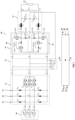
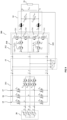
- FIG. 1 shows an electrical converter 10, referred to as the 'PRODRIVE-SELECT RECTIFIER', comprising two power stages 11, 12 in the form of a three-phase active phase selector 11 and an output power stage 12.
- Electrical converter 10 further comprises an input filter 13 placed between the phase selector 11 and the output power stage 12, and an output filter 14.
- an input filter (not shown) may be arranged upstream of the phase selector.
- the electrical converter 10 is an AC-to-DC converter that has three phase terminals A, B, C which are connected to a three-phase voltage of a three-phase AC grid 20, and a first and second output DC terminal P, N, here an upper output terminal P and a lower output terminal N, which for example may be connected to a DC load 21 such as, for example, a high voltage (e.g. 200 - 400 V) battery of an electric car.
- the phase selector 11 comprises three phase connections a, b, c that are connected to the three phase inputs A, B, C, and three outputs x, y, z.
- first intermediate node x here an upper intermediate voltage node x
- second intermediate node y here a lower intermediate voltage node y
- third intermediate node z here a middle intermediate voltage node z.
- the phase selector 11 comprises, or consists of, three bridge legs 15, 16, 17 which each comprise two passive semiconductor devices (diodes D ax and D ya for leg 15, D bx and D yb for leg 16, D cx and D yc for leg 17) connected in the form of a half bridge configuration, and three actively switchable semiconductor devices , here called selector switches S aza , S bzb , and S czc .
- each selector switch comprises two anti-series connected actively switchable semiconductor components.
- each such switchable semiconductor component includes or is complemented by an anti-parallel diode.
- MOSFETs Metal Oxide Field Effect Transistors
- an external anti-parallel diode may be provided.
- the output power stage 12 comprises, or consists of, two stacked (i.e. series connected) buck bridge legs 18, 19 of first and second stacked buck circuits.
- the first upper buck bridge leg 18 comprises a first semiconductor device 1p, a second semiconductor device 2p and a third semiconductor device 3p.
- the second lower buck bridge leg 19 comprises a fourth semiconductor device 1n, a fifth semiconductor device 2n and a sixth semiconductor device 3n.
- the second and fifth semiconductor device 2p, 2n is a buck switch ( S xp for the upper buck bridge leg 18 and S ny for the lower buck bridge leg 19).
- the switches S xp and S ny of the buck bridge legs 18, 19 are actively switchable semiconductor devices, for example MOSFETs.
- the third and sixth semiconductor device 3p, 3n is a buck diode ( D mp for the upper buck bridge leg 18 and D nm for the lower buck bridge leg 19).
- the second and third semiconductor devices 2p, 3p and the fifth and sixth semiconductor devices 2n, 3n are connected in a half-bridge configuration.
- the switched middle node of the upper buck bridge leg 18 forms an upper switch-node terminal p which is connected to output P via a first buck inductor, here an upper buck inductor L p
- the switched middle node of the lower buck bridge leg 19 forms a lower switch-node terminal n which is connected to output N via a second buck inductor, here a lower buck inductor L n .
- the common node m of both, stacked, buck bridge legs 18, 19 is connected to the midpoint of the output filter 14 which comprises two output filter capacitors C Pm , C mN that are connected in series between the upper output terminal P and the lower output terminal N.
- the first and fourth semiconductor device 1p, 1n of the first and second buck bridge leg 18, 19 is an interconnection switch S zp D zp and D nz S nz , with bi-directional voltage blocking capability, that allows for connecting the switched middle node of the respective bridge, i.e., the upper switch-node terminal p for the upper buck bridge leg 18 and the lower switch-node terminal n for the lower buck bridge leg 19, with the middle intermediate voltage node z.
- the interconnection switch S zp D zp of the upper buck bridge leg 18 comprises an actively switchable semiconductor component S zp , e.g.
- the interconnection switch D nz S nz of the lower buck bridge leg 19 comprises an actively switchable semiconductor component S nz , e.g. a MOSFET, connected in anti-series with a diode D nz , creating a voltage bi-directional interconnection switch.
- the upper buck bridge leg 18 is connected between the upper intermediate voltage node x and the common node m, and is arranged in a way that current can flow from the upper intermediate voltage node x to the upper output terminal P via the switch S xp when the switch S xp is closed (conducting, on state), current can flow from the middle intermediate voltage node z to the upper output terminal P via interconnection switch S zp D zp when the switch S zp is closed (conducting, on state) and the switch S xp is open (not conducting, off state), and current can flow from the common node m to the upper output terminal P via the diode D mp when the switches S xp and S zp are open (not conducting, off state).
- the lower buck bridge leg 19 is connected between the common node m and the lower intermediate voltage node y, and is arranged in a way that current can flow from the lower output terminal N to the lower intermediate voltage node y via the switch S ny when the switch S ny is closed (conducting, on state), current can flow from the lower output terminal N to the middle intermediate voltage node z via interconnection switch D nz S nz when the switch S nz is closed (conducting, on state) and the switch S ny is open (not conducting, off state), and current can flow from the lower output terminal N to the common node m via the diode D nm when the switches S ny and S nz are open (not conducting, off state).
- three high-frequency (HF) filter capacitors C x , C y , C z which are part of the input filter 13, are interconnecting the intermediate voltage nodes x, y, z in the form of a star-connection.
- the three capacitors C x , C y , C z have substantially equal value in order to symmetrically load the AC grid.
- the star point of the three high-frequency (HF) filter capacitors C x , C y , C z is connected to the common node m of both buck bridge legs 18, 19, and to the midpoint of the output filter 14.
- the bridge leg of the phase selector 11 that is connected with the phase input terminal A, B, or C that has the highest voltage of the three-phase AC input voltage is switched in a way that the corresponding phase input terminal A, B, or C is connected to the upper intermediate voltage node x.
- the bridge leg connects the corresponding phase connection a, b, or c with the node x via the upper diode D ax , D bx , D cx of the bridge leg, while the corresponding selector switch S aza , S bzb , S czc of the bridge leg is open (not conducting, off state).
- the bridge leg of the phase selector 11 that is connected with the phase input terminal A, B, or C that has the lowest voltage of the three-phase AC input voltage is switched in a way that the corresponding phase input terminal A, B, or C is connected to the lower intermediate voltage node y.
- the bridge leg connects the corresponding phase connection a, b, or c with the node y via the lower diode D ya , D yb , D yc of the bridge leg, while the corresponding selector switch S aza , S bzb , S czc of the bridge leg is open (not conducting, off state).
- the bridge leg of the phase selector 11 that is connected with the phase input terminal A, B, or C that has a voltage between the highest voltage and the lowest voltage of the three-phase AC input voltage is switched in a way that the corresponding phase input terminal A, B, or C is connected to the middle intermediate voltage node z.
- the bridge leg connects the corresponding phase connection a, b, or c with the node z via the selector switch S aza , S bzb , S czc which is closed (conducting, on state).
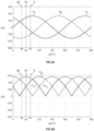
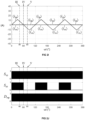
- the three-phase AC input voltage (mains voltage) is converted into three intermediate DC voltages v xz , v zy , v xy which are shown in FIG. 2B and which are provided between the upper intermediate voltage node x, the lower intermediate voltage node y and the middle intermediate voltage node z.
- These DC voltages thus show piece-wise sinusoidal shapes.
- the conversion of the three-phase AC input voltage into three intermediate DC voltages is the result of the operation of the phase selector 11, as explained above.
- the combination of states (conducting / not conducting) of the switches and diodes is unique for every 60° sector of the three-phase AC input voltage and depends on the voltage value of the phase inputs A, B, C.
- the sequence of the 6 unique states of the switches and diodes repeats itself every period (360°) of the AC mains voltage.
- a DC-DC buck circuit (upper buck circuit) can be identified, having three input ports x, z, m and two output ports P, m, and comprising the upper buck bridge leg 18, the upper buck inductor L p , and the upper output capacitor C Pm .
- V Pm v P - v m ( v P and v m are shown in FIG. 2D ) across the upper output capacitor C Pm .
- V Pm has a voltage value that is substantially equal to half the total DC bus voltage ( V Pm ⁇ V DC / 2 ) .
- an 'inversed' (negative input voltage and negative output voltage) DC-DC buck circuit (lower buck circuit) can be identified, having three input ports y, z, m and two output ports N, m, and comprising the lower buck bridge leg 19, the lower buck inductor L n , and the lower output capacitor C mN .
- V Nm v N - v m ( v N and v m are shown in FIG. 2D ) across the lower output capacitor C mN .
- V Nm has a voltage value that is substantially equal to minus half the total DC bus voltage ( V Nm ⁇ -V DC /2) .
- the upper switch-node terminal p of the upper buck bridge leg 18 can be alternately connected to the upper intermediate voltage node x, the middle intermediate voltage z, or the common node m. This results in a switched voltage v pm between nodes p and m, the switched voltage v pm which may thus have three voltage levels.
- the duty-ratios i.e.
- Control of these duty-ratios, and thus also control of the switching-cycle-averaged value ⁇ v pm ⁇ allows to control the switching-cycle-averaged value ⁇ i Lp ⁇ of the current i Lp in the upper buck inductor L p , e.g. using a closed-loop PI (Proportional-Integrating) control structure.
- a closed-loop PI Proportional-Integrating
- the lower switch-node terminal n of the lower buck bridge leg 19 can be alternately connected to the lower intermediate voltage node y, the middle intermediate voltage z, or the common node m. This results in a switched voltage v mn between nodes m and n, the switched voltage v mn which may thus have three voltage levels.
- the duty-ratios i.e.
- Control of these duty-ratios, and thus also control of the switching-cycle-averaged value ⁇ v nm ⁇ allows to control the switching-cycle-averaged value ⁇ i Ln ⁇ of the current i Ln in the lower buck inductor L N , e.g. using a closed-loop PI (Proportional-Integrating) control structure.
- a closed-loop PI Proportional-Integrating
- the HF components of currents i x , i y , i z at the input of the output power stage 12 are largely filtered by HF filter capacitors C x , C y , C z .
- the currents i' x , i' y , i' z at the output of the phase selector 11 are largely equal to the switching-cycle-averaged values ⁇ i x ⁇ , ⁇ i y ⁇ , ⁇ i z ⁇ of currents i x , i y , i z , i.e., i' x ⁇ ⁇ i x ⁇ , i' y ⁇ ⁇ i y ⁇ , i' z ⁇ ⁇ i z ⁇ .
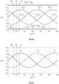
- FIG. 2E An example of the switching-cycle-averaged values ⁇ i Lp ⁇ , ⁇ i Ln ⁇ of currents i Lp , i Ln in the inductors L p , L n is shown in FIG. 2E .
- FIG. 2E Also shown in FIG. 2E is an example of the switching-cycle-averaged values ⁇ i y ⁇ , ⁇ i y ⁇ , ⁇ i z ⁇ of currents i y , i y , i z . As can be seen, these currents may be controlled to have piece-wise sinusoidal shapes.
- PFC Power Factor Correction
- the duty-ratio of the control signal of switch S nz equals zero during certain intervals within the line cycle of the mains voltage, i.e., in these intervals the switch S nz is continuously open (not conducting).
- this is the case for the intervals where v zy > v xz .
- FIG. 2I and 2E the switching-cycle-averaged value
- the duty-ratio of the control signal of switch S zp equals zero during certain intervals within the line cycle of the mains voltage, i.e., in these intervals the switch S zp is continuously open (not conducting).
- this is the case for the intervals where v zy ⁇ v xz .
- FIG. 2I , 2E As shown in FIG.
- the stepping down step performed by the upper and lower buck circuit comprises alternately (i.e. using a PWM signal) connecting the middle intermediate node z to an upper switch-node terminal p of the upper buck circuit during a first time interval T1 (where v zy > v xz ) and to a lower switch-node terminal n of the lower buck circuit during a second time interval T2 (where v zy ⁇ v xz ).
- the switch S zp is continuously switched on and off with a switching frequency and a first varying duty cycle and the switch S nz is off.
- the switch S zp is off, and the switch S nz is continuously switched on and off with a switching frequency and a second varying duty cycle.
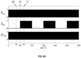
- FIG. 2J shows the states of the switches S xp and S zp of the upper buck bridge leg 18, and FIG. 2K shows the states of the switches S ny and S nz of the lower buck bridge leg 19, within a line cycle of the mains voltage.
- the switches S xp , S zp , S ny , S nz are all PWM modulated at a frequency (i.e. the switching frequency f s ; e.g. 100 kHz) that is substantially higher than the mains frequency (e.g. 50 Hz), as can be seen from the black-colored bars, indicating PWM modulation of the corresponding switch.
- switch S nz is continuously open (not conducting) during the intervals within the line cycle of the mains voltage where v zy > v xz
- switch S zp is continuously open (not conducting) during the intervals within the line cycle of the mains voltage where v zy ⁇ v xz .
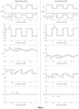
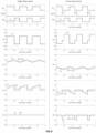
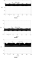
- FIGS. 3-5 show diagrams of currents, voltages, and switching signals on a milliseconds time axis, i.e. regarding three consecutive switching cycles of the bridge legs of the output power stage 12 of the electrical converter 10.
- Each switching cycle has a switching period T s equal to 1/ f s , with f s the switching frequency.
- the selector switches and diodes of the phase selector 11 are in the following switching states, see also FIG. 2C :
- FIGS. 3-5 The left columns ('upper buck circuit') of FIGS. 3-5 correspond with the operation of the upper buck circuit, while the right columns ('lower buck circuit') of FIGS. 3-5 correspond with the operation of the lower buck circuit.
- Each of FIGS. 3-5 shows:
- the semiconductor devices (switches and diodes) of the buck bridge legs 18, 19 of the output power stage 12 are sequentially conducting.
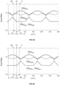
- the duty cycle of S xp (Dut Sxp ) may be increased and decreased synchronously with the voltage v x
- the duty cycle (Dut Sny ) of S ny may be increased and decreased synchronously with the voltage -v y
- the duty cycle of S zp (Dut Szp ) may be increased and decreased synchronously with the voltage v z when v zy > v xz
- the duty cycle of S nz (Dut Snz ) may be increased and decreased synchronously with the voltage v z when v zy ⁇ v xz .
- FIGs. 6A-E show respectively the currents i Lp , i Ln , i x , i y , i z within a whole line cycle (360°) of the mains voltage. Also shown are the switching-cycle-averaged values ⁇ i Lp ⁇ , ⁇ i Ln ⁇ , ⁇ i x ⁇ , ⁇ i y ⁇ , ⁇ i z ⁇ of these currents which correspond with the currents shown in FIG. 2E .
- the high-frequency ripple of phase currents i a , i b , i c is advantageously minimized, which is taken care of by the input filter 13.
- embodiments of the invention have the advantage that the currents can be lower. Indeed, when two buck circuits are connected in parallel between the upper and lower intermediate node, wherein one buck circuit is connected to the positive node and the other one to the negative node, one buck circuit sees the reverse current of the other buck circuit, resulting in higher currents. This disadvantage is not present when two buck circuits are connected in series between the upper and lower intermediate node as in embodiments of the invention.
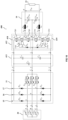
- an electrical converter 200 is shown which differs from converter 10 in that the third and sixth semiconductor devices 3p, 3n are different: diodes D mp , D nm of the output power stage 12 of the converter shown in FIG. 1 have been replaced with controllable semiconductor switches S pm , S mn , in this case MOSFETs, in the output power stage 212.
- This allows for the inductor current ⁇ i Lp ⁇ to also become negative within the conduction interval of S pm and for the inductor current ⁇ i Ln ⁇ to also become positive within the conduction interval of S mn , which was not possible for the implementation of the output power stage 12 with diodes ( D mp , D nm ) .
- FIGs. 8A-E show respectively the currents i Lp , i Ln , i x , i y , i z within a whole line cycle (360°) of the mains voltage in case of ZVS operation of output power stage 212.
- the electrical converters 10 (shown in FIG. 1 ) and 200 (shown in FIG. 7 ) are unidirectional since the phase selector 11 and the output power stages 12, 212 contain diodes, only allowing power to be drawn from the electrical AC grid 20 and provide this power at the output to a load 21.
- FIG. 9 shows an electrical converter 300 that is bidirectional.
- Electrical converter 300 differs from converters 10, 200 in that the diodes D ax , D bx , D cx , D ya , D yb , D yc of the phase selector 11 and the diodes D zp , D mp , D nz , D nm of the output power stages 12, 212 have been replaced with controllable semiconductor switches S xa , S xb , S xc , S ay , S by , S cy in the phase selector 311 and S pz , S pm , S zn , S mn in the output power stage 312, respectively.
- the electrical converter 300 may be used as a DC-to-AC converter with A, B, C being the output terminals and P, N the input terminals, as will be clear to a person skilled in the art. This may be useful e.g. in applications using solar cells.
- FIG. 10 another electrical converter 400 is shown which differs from converter 10 in that the stacked buck bridge legs 18, 19 of the output power stage 412 are implemented using a different configuration of the first, second, third, fourth, fifth, and sixth semiconductor devices 1p, 2p, 3p, 1n, 2n, 3n, providing the same functionality. Also, in the electrical converter 400, the HF capacitors C xy , C xz , C zy which interconnect the intermediate voltage nodes x, y, z are connected in a delta configuration instead of a star configuration.
- diodes may be replaced by actively switchable semiconductor devices to allow for bidirectional power flow of the electrical converter (as in the embodiment of FIG. 9 ).
- the HF capacitors C x , C x , C z , C xy , C xz , C zy may be placed between the phase input terminals A, B, C and the phase selector 11, 311, and interconnect the phase input terminals A, B, C in the form of a star or delta configuration.
- a combination of a set of HF capacitors which interconnect the intermediate voltage nodes x, y, z (as in electrical converters 10, 200, 300, 400) and a set of HF capacitors which interconnect the phase input terminals A, B, C, either in the form of a star or delta configuration, or a combination, may also be used.
- the HF capacitors C x , C y , C z are connected in a star configuration.
- a delta configuration of these capacitors may be used in either of these electrical converters.
- the HF capacitors C xy , C xz , C zy are connected in a delta configuration. Alternatively, a star configuration of these capacitors may be used.
- FIG. 11 another electrical converter 500 is shown which differs from converter 200 in that the output filter 14 is replaced by an active output filter 514 that includes a boost stage.
- An active output filter may be used in the electrical converters of either FIG. 1 , FIG. 7 , FIG. 9 , FIG. 10 .
- FIG. 12A, 12B show different variants of the three-phase phase selector 11, which may be used in the electrical converters of either FIG. 1 , FIG. 7 , FIG. 9 , FIG. 10 , FIG. 11 .
- each actively switchable semiconductor device S aza , S bzb , and S czc comprises four diodes and a transistor with an anti-parallel diode.
- S aza , S bzb , and S czc comprises four diodes and a transistor with an anti-parallel diode.
- each actively switchable semiconductor device S aza , S bzb , and S czc comprises four diodes and a transistor with an anti-parallel diode, and the semiconductor device S aza , S bzb , and S czc are included in the legs 15, 16, 17, respectively. It is noted that when the transistor of the semiconductor device S aza , S bzb , and S czc is off (i.e. does not conduct) current in the legs 15, 16, 17 can still flow through the diodes of the semiconductor device S aza , S bzb , and S czc .
- a central control unit 40 may be used which controls all the controllable semiconductor devices (switches) of the electrical converter 10, sending control signals to each switch via a communication interface 50.
- semiconductor devices S aza , S bzb , S czc , S xp , S ny , S zp , S nz are controlled by controller 40.
- the control unit has measurement input ports 42, 43, 44, 45, 46, for receiving measurements of:
- FIG. 13 shows a block diagram of an advantageous implementation of the central control unit 40 which is shown in a schematically way in FIG. 1 .
- the electrical converter 10 is represented in FIG. 13 as a 'single-wire' equivalent circuit, wherein the annotations of the elements correspond with those given in FIG. 1 .
- Three slashes in a signal line indicate the bundling of multiple signals, and may represent the transition to a vector representation.
- the goal of the control unit 40 is to control the output voltage V DC to a requested set-value V DC ⁇ that is received from an external unit via input port 41, and to balance the voltage across the two output capacitors C Pm and C mN , for example by controlling the voltage across the lower output capacitor C mN to be substantially equal to half the DC bus voltage. Additionally, the current drawn from the phase inputs (a, b, c) needs to be shaped substantially sinusoidal and controlled substantially in phase with the corresponding phase voltage.
- the control of the output voltage V DC is advantageously done using a cascaded control structure, comprising an outer voltage control loop 60 and inner current control loop 70.
- the set-value of the output voltage is input to a comparator 61 via input port 41, and is compared with the measured output voltage obtained from a measurement means 95 (for example comprising a low-pass filter).
- the output of comparator 61 is the control-error signal of the output voltage, which is further input to a control element 62 (for example comprising a proportional-integral control block) that outputs instantaneous set-values related to the phase currents and/or set-values related to the DC component of the inductor currents.
- the inputs of calculation element 64 are the measured phase voltages v a , v b , v c obtained from a measurement means 93 (for example comprising a low-pass filter).
- the output of the multiplier 63 are set-values i a ⁇ , i b ⁇ , i c ⁇ , i Lp ⁇ , i Ln ⁇ for the instantaneous, for example low-pass filtered, phase currents i a , i b , i c , and the instantaneous, for example low-pass filtered, DC component of inductor currents i Lp , i Ln .
- Set-values i a ⁇ , i b ⁇ , i c ⁇ are shaped substantially sinusoidal and positioned substantially in phase with the corresponding phase voltages.
- the set-values i a ⁇ , i b ⁇ , i c ⁇ , i Lp ⁇ , i Ln ⁇ are input to the current controller 70 after passing an addition element 67 and a selection element 81 whose functions are further detailed in the following text.
- the current controller 70 is split into five individual current controllers 71, 72, 73, 74, 75, wherein:
- Selector element 81 is used to send the set-values i a ⁇ , i b ⁇ , i c ⁇ , i Lp ⁇ , i Ln ⁇ , for the instantaneous phase currents and inductor currents to the correct individual current controller 71, 72, 73, 74, 75 depending on the voltage value of the phase inputs A, B, C, resulting in intermediate current set-values i x ′ ⁇ , i y ′ ⁇ , i z ′ ⁇ and inductor current set-values i Lp ⁇ , i Ln ⁇ for each individual current controller, wherein:
- each individual current controller the received set-value i x ′ ⁇ , i y ′ ⁇ , i z ′ ⁇ , i Lp ⁇ , i Ln ⁇ for the instantaneous current is input to a comparator, for example comparator 76 of individual current controller 71, and compared with the measured current i x , measured ′ , i y , measured ′ , i z , measured ′ , i Lp , measured , i Ln,measured obtained from a measurement means 94 (for example comprising a low-pass filter) and from a measurement means 97.
- a measurement means 94 for example comprising a low-pass filter
- the output of the comparator is the control-error signal of the current, which is further input to a control element, for example control element 77 (for example a proportional-integral controller) of individual current controller 71.
- the output of current controller 70 which is for example a bundled combination of outputs of individual current controllers 71, 72, 73, 74, 75 is input to a PWM generation element, for example PWM generation element 54.
- the PWM generation element generates the PWM-modulated control signals for the controllable semiconductor switches of the PWM-controlled bridge legs, i.e. the upper buck bridge leg 18 of the upper buck circuit and the lower buck bridge leg 19 of the lower buck circuit. These PWM-modulated control signals are sent to the appropriate bridge legs via communication interface 50.
- phase currents i a , i b , i c shown in FIG. 2F are obtained by controlling the electrical converter 10 using such control unit 40 and control method detailed in the foregoing text.
- the phase currents i a , i b , i c are indirectly controlled, i.e., they are the result of the controlling of the intermediate currents i x ′ , i y ′ , i z ′ (shown in FIG. 2E ) and/or the inductor currents i Lp , i Ln and of the operation of the phase selector 11.
- the set-points for the intermediate currents i x ′ ⁇ , i y ′ ⁇ , i z ′ ⁇ are derived from set-values i a ⁇ , i b ⁇ , i c ⁇ by selector element 81 based on the measured phase voltages.
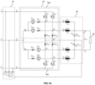
- FIG. 14 another output stage 12 is shown in which the stacked series connected buck bridge legs 18, 19 of FIG. 1 are replaced by a first parallel connection of upper bridge legs 718 and a second parallel connection of lower bridge legs 719, wherein the first parallel connection of upper bridge legs 718 is connected in series with the second parallel connection of lower bridge legs 719.
- the first parallel connection of buck bridge legs 718 comprises two first semiconductor devices, two second semiconductor devices and two third semiconductor devices.
- the parallel connection of second buck bridge legs 719 comprises two fourth semiconductor devices, two fifth semiconductor node terminals n1, n2 for the lower buck bridge legs 719, with the middle intermediate voltage node z.
- FIG. 14 another output stage 12 is shown in which the stacked series connected buck bridge legs 18, 19 of FIG. 1 are replaced by a first parallel connection of upper bridge legs 718 and a second parallel connection of lower bridge legs 719, wherein the first parallel connection of upper bridge legs 718 is connected in series with the second parallel connection of lower bridge legs 719.
- the output stage may be scaled by providing multiple first upper buck circuits in parallel and by providing multiple second lower buck circuits in parallel. This may be useful, e.g. when more power is needed.
- first and second buck circuits When multiple first and second buck circuits are connected in parallel as in FIG. 14 , such respective first and second buck circuits may be controlled in an interleaved way.
- controller may be provided through the use of dedicated hardware as well as hardware capable of executing software in association with appropriate software.
- the functions may be provided by a single dedicated processor, by a single shared processor, or by a plurality of individual processors, some of which may be shared.
- explicit use of the term "controller” should not be construed to refer exclusively to hardware capable of executing software, and may implicitly include, without limitation, digital signal processor (DSP) hardware, network processor, application specific integrated circuit (ASIC), field programmable gate array (FPGA), read only memory (ROM) for storing software, random access memory (RAM), and non volatile storage.
- DSP digital signal processor
- ASIC application specific integrated circuit
- FPGA field programmable gate array
- ROM read only memory
- RAM random access memory
- non volatile storage Other hardware, conventional and/or custom, may also be included.
Landscapes
- Engineering & Computer Science (AREA)
- Power Engineering (AREA)
- Transportation (AREA)
- Mechanical Engineering (AREA)
- Dc-Dc Converters (AREA)
- Rectifiers (AREA)
Claims (15)
- Elektrischer Wandler (10) zur Wandlung zwischen einem dreiphasigen Wechselstromsignal und einem Gleichstromsignal, umfassend:drei Phasenanschlüsse (A, B, C)einen ersten Gleichstromanschluss (P) und einen zweiten Gleichstromanschluss (N),eine Phasenwahleinrichtung (11) zum Verbinden der drei Phasenanschlüsse mit einem ersten Zwischenknoten (x), einem zweiten Zwischenknoten (y) und einem dritten Zwischenknoten (z) des elektrischen Wandlers,eine ersten Abwärtsschaltung, die einen ersten Schaltknotenanschluss (p) umfasst, der betriebsfähig mit dem ersten Gleichstromanschluss (P) verbunden ist, und eine zweite Abwärtsschaltung, die einen zweiten Schaltknotenanschluss (n) umfasst, der betriebsfähig mit dem zweiten Gleichstromanschluss (N) verbunden ist, wobei die erste und die zweite Abwärtsschaltung zum Wandeln einer Spannung an dem ersten Zwischenknoten (x), dem zweiten Zwischenknoten (y) und dem dritten Zwischenknoten (z) in eine Spannung zwischen dem ersten und dem zweiten Gleichstromanschluss (P, N) verbunden sind,wobei die erste und die zweite Abwärtsschaltung zwischen dem ersten Zwischenknoten (x) und dem zweiten Zwischenknoten (y) derart in Reihe geschaltet sind, dass ein gemeinsamer Knoten (m) der ersten und der zweiten Abwärtsschaltung vorhanden ist, wobei die erste und die zweite Abwärtsschaltung mindestens eine aktiv schaltbare Vorrichtung umfassen, die zwischen dem gemeinsamen Knoten und dem dritten Zwischenknoten verbunden ist,gekennzeichnet dadurch, dass die erste Abwärtsschaltung dazu konfiguriert ist, das Verbinden des ersten Schaltknotenanschlusses (p) mit einem beliebigen aus dem ersten Zwischenknoten (x), dem dritten Zwischenknoten (z) und dem gemeinsamen Knoten (m) zu ermöglichen, und dadurch, dass die zweite Abwärtsschaltung dazu konfiguriert ist, das Verbinden des zweiten Schaltknotenanschlusses (n) mit einem beliebigen aus dem zweiten Zwischenknoten (y), dem dritten Zwischenknoten (z) und dem gemeinsamen Knoten (m) zu ermöglichen.
- Elektrischer Wandler nach Anspruch 1, wobei die erste Abwärtsschaltung Folgendes umfasst:eine erste Vorrichtung (1p), die zum Unterbrechen eines Stromflusses zwischen dem ersten Schaltknotenanschluss (p) und dem dritten Zwischenknoten (z) verbunden ist;eine zweite Vorrichtung (2p), die zum Unterbrechen eines Stromflusses zwischen dem ersten Schaltknotenanschluss (p) und dem ersten Zwischenknoten (x) verbunden ist;eine dritte Vorrichtung (3p), die zum Unterbrechen eines Stromflusses zwischen dem ersten Schaltknotenanschluss (p) und dem gemeinsamen Knoten verbunden ist;wobei mindestens zwei aus der ersten, der zweiten und der dritten Vorrichtung der ersten Abwärtsschaltung aktiv schaltbar sind; undwobei die zweite Abwärtsschaltung Folgendes umfasst:wobei bevorzugt die erste Vorrichtung und die vierte Vorrichtung aktiv schaltbar sind, und die mindestens eine aktiv schaltbare Vorrichtung die erste Vorrichtung und die vierte Vorrichtung umfasst.eine vierte Vorrichtung (1n), die zum Unterbrechen eines Stromflusses zwischen dem zweiten Schaltknotenanschluss (n) und dem dritten Zwischenknoten (z) verbunden ist;eine fünfte Vorrichtung (2n), die zum Unterbrechen eines Stromflusses zwischen dem zweiten Schaltknotenanschluss (n) und dem zweiten Zwischenknoten (y) verbunden ist; undeine sechste Vorrichtung (3n), die zum Unterbrechen eines Stromflusses zwischen dem zweiten Schaltknotenanschluss (n) und dem gemeinsamen Knoten (m) verbunden ist, wobei mindestens zwei aus der vierten, der fünften und der sechsten Vorrichtung der zweiten Abwärtsschaltung aktiv schaltbar sind,
- Elektrischer Wandler nach Anspruch 2, wobei mindestens eine aus der zweiten Vorrichtung und der dritten Vorrichtung und mindestens eine aus der fünften Vorrichtung und der sechsten Vorrichtung aktiv schaltbar sind.
- Elektrischer Wandler nach einem der vorhergehenden Ansprüche, wobei die Phasenwahleinrichtung Vorrichtungen (Saza, Sbzb, Sczc) umfasst, die zum selektiven Verbinden des dritten Zwischenknotens mit den drei Phasenanschlüssen aktiv schaltbar sind.
- Elektrischer Wandler nach einem der vorhergehenden Ansprüche, ferner umfassend eine Steuereinheit (40), die dazu konfiguriert ist, mindestens eine aus der Phasenwahleinrichtung und der ersten und der zweiten Abwärtsschaltung zu steuern, wobei die Phasenwahleinrichtung (11) und die Steuereinheit (40) derart konfiguriert sind, dass das Schalten der Vorrichtungen der Phasenwahleinrichtung gemäß einem Schaltmuster gesteuert wird, in dem:der Phasenanschluss, der eine höchste Spannung aufweist, mit dem ersten Zwischenknoten verbunden ist,der Phasenanschluss, der eine niedrigste Spannung aufweist, mit dem zweiten Zwischenknoten verbunden ist, undder Phasenanschluss, der eine Zwischenspannung zwischen der höchsten Spannung und der niedrigsten Spannung aufweist, mit dem dritten Zwischenknoten verbunden ist,wobei bevorzugt die Steuereinheit dazu konfiguriert ist, mindestens einen Arbeitszyklus, eine Schaltfrequenz und eine Leitungssequenz von Steuersignalen zu steuern, die verwendet werden, um die erste Abwärtsschaltung und die zweite Abwärtsschaltung zu steuern.
- Elektrischer Wandler nach einem der vorhergehenden Ansprüche, wobei die erste und die zweite Abwärtsschaltung jeweils eine erste Filterspule (Lp), die zwischen dem ersten Schaltknotenanschluss (p) und dem ersten Gleichstromanschluss (P) verbunden ist, und eine zweite Filterspule (Ln), die zwischen dem zweiten Schaltknotenanschluss (n) und dem zweiten Gleichstromanschluss (N) verbunden ist, umfassen.
- Elektrischer Wandler nach einem der vorhergehenden Ansprüche, ferner umfassend mindestens einen Filterkondensator, bevorzugt eine Reihenverbindung von mindestens zwei Filterkondensatoren (CPm, CmN), die zwischen dem ersten und dem zweiten Gleichstromanschluss (P, N) verbunden sind, wobei bevorzugt der gemeinsame Knoten (m) mit einem Mittelpunkt der Reihenverbindung der mindestens zwei Filterkondensatoren verbunden ist.
- Elektrischer Wandler nach einem der vorhergehenden Ansprüche, umfassend einen Filter (13), der Kondensatoren (Cx, Cy, Cz; Cxy, Cxz, Czy) umfasst, die die Zwischenknoten (x, y, z), bevorzugt in der Form einer Stern- oder einer Deltaverbindung, verbinden, wobei bevorzugt die Kondensatoren (Cx, Cy, Cz) in einer Sternverbindung miteinander verbunden sind, und wobei der gemeinsame Knoten (m) mit einem Sternpunkt der Sternverbindung verbunden ist.
- Elektrischer Wandler nach Anspruch 5, optional in Kombination mit einem der vorhergehenden Ansprüche, umfassend Messmittel (93, 94, 95, 96, 97), die zum Messen von mindestens einem aus dem Gleichstromsignal, einem das Gleichstromsignal beeinflussenden elektrischen Signal, einem von dem Gleichstromsignal beeinflussten elektrischen Signal konfiguriert sind, und wobei die Steuereinheit (40) eine Steuerschleife (71-75) umfasst, die dazu konfiguriert ist, mindestens eines aus einem Arbeitszyklus, einer Schaltfrequenz und einer Leitungssequenz von Kontrollsignalen anzupassen, um mindestens eine aus der ersten und der zweiten Abwärtsschaltung auf Basis von Messungen der Messmittel zu steuern, wobei die Messmittel bevorzugt mindestens eines aus den Folgenden umfassen: ein Strommessmittel (97) zum Messen von mindestens einem aus einem Strom zwischen dem ersten Schaltknotenanschluss (p) und dem ersten Gleichstromanschluss (P) und einem Strom zwischen dem zweiten Schaltknotenanschluss (n) und dem zweiten Gleichstromanschluss (N), ein Spannungsmessmittel (93) zum Messen von Spannungen an den drei Phasenanschlüssen, ein Spannungsmessmittel (95) zum Messen einer Spannung zwischen dem zweiten und dem ersten Gleichstromanschluss, ein Strommessmittel (94) zum Messen eines Stroms zwischen der Phasenwahleinrichtung und einem aus dem ersten, dem dritten und dem zweiten Zwischenknoten, ein Spannungsmessmittel (96) zum Messen einer Spannung des gemeinsamen Knotens.
- Elektrischer Wandler nach einem der vorhergehenden Ansprüche, wobei die Phasenwahleinrichtung drei Wahleinrichtungszweige (16, 17, 18) zum Verbinden von einem der drei Phasenanschlüsse mit dem ersten Zwischenknoten (x), dem zweiten Zwischenknoten (y) und dem dritten Zwischenknoten (z) umfasst, wobei jeder der drei Wahleinrichtungszweige eine Halbbrücke umfasst, die Schalter (Dax, Dbx, Dcx, Dya, Dyb, Dyc, Sxa, Sxb, Sxc, Say, Sby, Scy ) umfasst.
- Batterieladesystem, insbesondere zum Laden einer Batterie eines elektrischen Fahrzeugs, umfassend eine Energieversorgungseinheit, wobei die Energieversorgungseinheit den elektrischen Wandler nach einem der vorhergehenden Ansprüche umfasst.
- Elektrisches Motorantriebssystem, umfassend eine Energieversorgungseinheit, wobei die Energieversorgungseinheit den elektrischen Wandler nach einem der Ansprüche 1 bis 10 umfasst.
- Gradientenverstärker, umfassend den elektrischen Wandler nach einem der Ansprüche 1 bis 10.
- Verfahren zum Wandeln zwischen einem dreiphasigen Wechselstromsignal und einem Gleichstromsignal, umfassend:Wandeln zwischen dem dreiphasigen Wechselstromsignal und einem Zwischensignal, wobei das Zwischensignal zwischen einem ersten Zwischenknoten (x), einem zweiten Zwischenknoten (y) und einem dritten Zwischenknoten (z) angewendet wird, wobei eine Spannung des dreiphasigen Wechselstromsignals selektiv auf den ersten Zwischenknoten (x), den zweiten Zwischenknoten (y) und dem dritten Zwischenknoten (z) angewendet wird,Wandeln zwischen den Zwischensignalen und dem Gleichstromsignal unter Verwendung einer ersten und einer zweiten Abwärtsschaltung, wobei die erste und die zweite Abwärtsschaltung zwischen dem ersten Zwischenknoten (x) und dem zweiten Zwischenknoten (y) derart in Reihe geschaltet sind, dass ein gemeinsamer Knoten (m) der ersten und der zweiten Abwärtsschaltung vorhanden ist, wobei das Wandeln das Verbinden des dritten Zwischenknotens (z) mit einem ersten Schaltknotenanschluss (p) der ersten Abwärtsschaltung während eines ersten Zeitintervalls (T1) und mit einem zweiten Schaltknotenanschluss (n) der zweiten Abwärtsschaltung während eines zweiten Zeitintervalls (T2) umfasst, unter Verwendung von mindestens einer aktiv schaltbaren Vorrichtung zwischen dem gemeinsamen Knoten und dem dritten Zwischenknoten,wobei das Wandeln zwischen den Zwischensignalen und dem Gleichstromsignal unter Verwendung einer ersten und einer zweiten Abwärtsschaltung das Verbinden des ersten Schaltknotenanschlusses (p) mit einem beliebigen aus dem ersten Zwischenknoten (x), dem dritten Zwischenknoten (z) und dem gemeinsamen Knoten (m) und das Verbinden des zweiten Schaltknotenanschlusses (n) mit einem beliebigen aus dem zweiten Zwischenknoten (y), dem dritten Zwischenknoten (z) und dem gemeinsamen Knoten (m) umfasst.
- Verfahren nach Anspruch 14, wobei eine Spannung des dreiphasigen Wechselstromsignals, das eine höchste Spannung aufweist, auf den ersten Zwischenknoten (x) angewendet wird, eine Spannung des dreiphasigen Wechselstromsignals, das eine niedrigste Spannung aufweist, auf den zweiten Zwischenknoten (y) angewendet wird und eine Spannung des dreiphasigen Wechselstromsignals, das eine Zwischenspannung zwischen der höchsten Spannung und der niedrigsten Spannung aufweist, auf den dritten Zwischenknoten (z) angewendet wird,
wobei bevorzugt das Wandeln zwischen dem Zwischensignal und dem Gleichstromsignal unter Verwendung einer ersten und einer zweiten Abwärtsschaltung Folgendes umfasst:aktives Steuern einer ersten schaltbaren Vorrichtung (1p), die zwischen dem dritten Zwischenknoten (z) und dem ersten Schaltknotenanschluss (p) verbunden ist, und einer vierten schaltbaren Vorrichtung (1n) zwischen dem dritten Zwischenknoten (z) und dem zweiten Schaltknotenanschluss (n);aktives Steuern von mindestens einer aus einer zweiten schaltbaren Vorrichtung (2p), die zwischen dem ersten Zwischenknoten (x) und dem ersten Schaltknotenanschluss (p) verbunden ist, und einer dritten schaltbaren Vorrichtung (3p), die zwischen dem gemeinsamen Knoten (m) und dem ersten Schaltknotenanschluss (p) verbunden ist;aktives Steuern von mindestens einer aus einer fünften schaltbaren Vorrichtung (2n) zwischen dem zweiten Zwischenknoten (y) und dem zweiten Schaltknotenanschluss (n) und einer sechsten schaltbaren Vorrichtung (3n) zwischen dem gemeinsamen Knoten (m) und dem zweiten Schaltknotenanschluss (n).
Applications Claiming Priority (2)
| Application Number | Priority Date | Filing Date | Title |
|---|---|---|---|
| NL2022950A NL2022950B1 (en) | 2019-04-15 | 2019-04-15 | Electrical Converter |
| PCT/EP2020/060308 WO2020212278A1 (en) | 2019-04-15 | 2020-04-10 | Electrical converter |
Publications (3)
| Publication Number | Publication Date |
|---|---|
| EP3956972A1 EP3956972A1 (de) | 2022-02-23 |
| EP3956972C0 EP3956972C0 (de) | 2025-06-04 |
| EP3956972B1 true EP3956972B1 (de) | 2025-06-04 |
Family
ID=66380099
Family Applications (1)
| Application Number | Title | Priority Date | Filing Date |
|---|---|---|---|
| EP20716521.8A Active EP3956972B1 (de) | 2019-04-15 | 2020-04-10 | Elektrischer wandler |
Country Status (6)
| Country | Link |
|---|---|
| US (1) | US11881792B2 (de) |
| EP (1) | EP3956972B1 (de) |
| CN (1) | CN113812078A (de) |
| NL (1) | NL2022950B1 (de) |
| TW (1) | TW202046622A (de) |
| WO (1) | WO2020212278A1 (de) |
Families Citing this family (11)
| Publication number | Priority date | Publication date | Assignee | Title |
|---|---|---|---|---|
| CN113726137B (zh) * | 2020-05-26 | 2023-11-03 | 台达电子企业管理(上海)有限公司 | 变换装置 |
| CN113726136B (zh) * | 2020-05-26 | 2023-11-03 | 台达电子企业管理(上海)有限公司 | 变换装置 |
| US12083912B2 (en) | 2021-03-18 | 2024-09-10 | Delta Electronics, Inc. | Electric system of electric vehicle |
| DE102021108996A1 (de) * | 2021-04-12 | 2022-10-13 | Ebm-Papst Mulfingen Gmbh & Co. Kg | Schaltungsanordnung |
| US11777414B2 (en) * | 2021-07-02 | 2023-10-03 | Schneider Electric It Corporation | Interleaved power conversion systems and methods |
| US11646671B1 (en) * | 2021-10-12 | 2023-05-09 | Utah State University | Unfolder-based single-stage AC-AC conversion system |
| CN114337305A (zh) * | 2021-12-31 | 2022-04-12 | 苏州汇川控制技术有限公司 | 直流电压变换电路及装置 |
| TWI829114B (zh) * | 2022-03-18 | 2024-01-11 | 台達電子工業股份有限公司 | 電動車的電力系統 |
| CN115360916B (zh) * | 2022-09-23 | 2025-05-13 | 珠海格力电器股份有限公司 | 一种Buck-Boost变换电路和光伏发电系统 |
| CN115593248A (zh) * | 2022-10-31 | 2023-01-13 | 上海万暨电子科技有限公司(Cn) | 一种电动汽车无线充电系统 |
| US20250274049A1 (en) * | 2024-02-24 | 2025-08-28 | Utah State University | High-bandwidth control of unfolding-based ac-dc converters |
Family Cites Families (9)
| Publication number | Priority date | Publication date | Assignee | Title |
|---|---|---|---|---|
| US5784269A (en) * | 1997-02-21 | 1998-07-21 | Lucent Technologies, Inc. | Three phase high power factor converter using phase selection circuit |
| US6046915A (en) * | 1997-02-21 | 2000-04-04 | Lucent Technologies Inc. | Phase selection circuit for three phase power converter and method of operation thereof |
| US5946203A (en) * | 1998-07-17 | 1999-08-31 | Lucent Technologies Inc. | Switching network and method of reducing input current total harmonic distortion associated with a boost converter and a boost converter employing the switching network or method |
| WO2013121580A1 (ja) | 2012-02-17 | 2013-08-22 | パイオニア株式会社 | 直管形発光灯 |
| AT512752B1 (de) * | 2012-03-30 | 2018-02-15 | Schneider Electric Power Drives Gmbh | Gleichrichterschaltung mit Strominjektion |
| US9444363B1 (en) * | 2015-02-24 | 2016-09-13 | Infineon Technologies Austria Ag | Circuit arrangement with a rectifier circuit |
| FR3061819B1 (fr) * | 2017-01-12 | 2021-06-18 | Renault Sas | Chargeur de batterie d'accumulateurs electriques bidirectionnel. |
| CH713573B1 (de) * | 2017-03-15 | 2021-01-29 | Eth Zuerich | Magnetische Drossel, Umrichterabschnitt und Umrichter. |
| US10917019B2 (en) * | 2019-03-11 | 2021-02-09 | Utah State University | Quasi-single stage power converter topology |
-
2019
- 2019-04-15 NL NL2022950A patent/NL2022950B1/en active
-
2020
- 2020-04-09 TW TW109111944A patent/TW202046622A/zh unknown
- 2020-04-10 CN CN202080035304.5A patent/CN113812078A/zh active Pending
- 2020-04-10 WO PCT/EP2020/060308 patent/WO2020212278A1/en not_active Ceased
- 2020-04-10 EP EP20716521.8A patent/EP3956972B1/de active Active
- 2020-04-10 US US17/603,238 patent/US11881792B2/en active Active
Also Published As
| Publication number | Publication date |
|---|---|
| TW202046622A (zh) | 2020-12-16 |
| WO2020212278A1 (en) | 2020-10-22 |
| NL2022950B1 (en) | 2020-10-22 |
| US11881792B2 (en) | 2024-01-23 |
| EP3956972C0 (de) | 2025-06-04 |
| US20220190744A1 (en) | 2022-06-16 |
| EP3956972A1 (de) | 2022-02-23 |
| CN113812078A (zh) | 2021-12-17 |
Similar Documents
| Publication | Publication Date | Title |
|---|---|---|
| EP3956972B1 (de) | Elektrischer wandler | |
| EP3837759B1 (de) | Stromwandler | |
| EP3874588B1 (de) | Stromwandler | |
| US20230238876A1 (en) | Electrical power converter | |
| EP4147341B1 (de) | Elektrischer leistungswandler | |
| US20220278607A1 (en) | Electrical converter | |
| EP4147340B1 (de) | Elektrischer leistungswandler | |
| EP4147338B1 (de) | Elektrischer leistungswandler mit vorladebetrieb | |
| NL2023292B1 (en) | Electrical Converter |
Legal Events
| Date | Code | Title | Description |
|---|---|---|---|
| STAA | Information on the status of an ep patent application or granted ep patent |
Free format text: STATUS: UNKNOWN |
|
| STAA | Information on the status of an ep patent application or granted ep patent |
Free format text: STATUS: THE INTERNATIONAL PUBLICATION HAS BEEN MADE |
|
| PUAI | Public reference made under article 153(3) epc to a published international application that has entered the european phase |
Free format text: ORIGINAL CODE: 0009012 |
|
| STAA | Information on the status of an ep patent application or granted ep patent |
Free format text: STATUS: REQUEST FOR EXAMINATION WAS MADE |
|
| 17P | Request for examination filed |
Effective date: 20211105 |
|
| AK | Designated contracting states |
Kind code of ref document: A1 Designated state(s): AL AT BE BG CH CY CZ DE DK EE ES FI FR GB GR HR HU IE IS IT LI LT LU LV MC MK MT NL NO PL PT RO RS SE SI SK SM TR |
|
| DAV | Request for validation of the european patent (deleted) | ||
| DAX | Request for extension of the european patent (deleted) | ||
| GRAP | Despatch of communication of intention to grant a patent |
Free format text: ORIGINAL CODE: EPIDOSNIGR1 |
|
| STAA | Information on the status of an ep patent application or granted ep patent |
Free format text: STATUS: GRANT OF PATENT IS INTENDED |
|
| RIC1 | Information provided on ipc code assigned before grant |
Ipc: H02M 7/487 20070101ALI20240924BHEP Ipc: H02M 1/12 20060101ALI20240924BHEP Ipc: H02M 7/797 20060101ALI20240924BHEP Ipc: H02M 1/00 20060101ALI20240924BHEP Ipc: H02M 7/219 20060101ALI20240924BHEP Ipc: H02M 3/158 20060101ALI20240924BHEP Ipc: H02M 1/42 20070101AFI20240924BHEP |
|
| INTG | Intention to grant announced |
Effective date: 20241017 |
|
| GRAJ | Information related to disapproval of communication of intention to grant by the applicant or resumption of examination proceedings by the epo deleted |
Free format text: ORIGINAL CODE: EPIDOSDIGR1 |
|
| STAA | Information on the status of an ep patent application or granted ep patent |
Free format text: STATUS: REQUEST FOR EXAMINATION WAS MADE |
|
| GRAP | Despatch of communication of intention to grant a patent |
Free format text: ORIGINAL CODE: EPIDOSNIGR1 |
|
| STAA | Information on the status of an ep patent application or granted ep patent |
Free format text: STATUS: GRANT OF PATENT IS INTENDED |
|
| INTC | Intention to grant announced (deleted) | ||
| INTG | Intention to grant announced |
Effective date: 20250207 |
|
| GRAS | Grant fee paid |
Free format text: ORIGINAL CODE: EPIDOSNIGR3 |
|
| GRAA | (expected) grant |
Free format text: ORIGINAL CODE: 0009210 |
|
| STAA | Information on the status of an ep patent application or granted ep patent |
Free format text: STATUS: THE PATENT HAS BEEN GRANTED |
|
| AK | Designated contracting states |
Kind code of ref document: B1 Designated state(s): AL AT BE BG CH CY CZ DE DK EE ES FI FR GB GR HR HU IE IS IT LI LT LU LV MC MK MT NL NO PL PT RO RS SE SI SK SM TR |
|
| REG | Reference to a national code |
Ref country code: GB Ref legal event code: FG4D |
|
| REG | Reference to a national code |
Ref country code: CH Ref legal event code: EP |
|
| REG | Reference to a national code |
Ref country code: DE Ref legal event code: R096 Ref document number: 602020052256 Country of ref document: DE |
|
| REG | Reference to a national code |
Ref country code: IE Ref legal event code: FG4D |
|
| U01 | Request for unitary effect filed |
Effective date: 20250611 |
|
| U07 | Unitary effect registered |
Designated state(s): AT BE BG DE DK EE FI FR IT LT LU LV MT NL PT RO SE SI Effective date: 20250620 |
|
| PG25 | Lapsed in a contracting state [announced via postgrant information from national office to epo] |
Ref country code: ES Free format text: LAPSE BECAUSE OF FAILURE TO SUBMIT A TRANSLATION OF THE DESCRIPTION OR TO PAY THE FEE WITHIN THE PRESCRIBED TIME-LIMIT Effective date: 20250604 |
|
| PG25 | Lapsed in a contracting state [announced via postgrant information from national office to epo] |
Ref country code: NO Free format text: LAPSE BECAUSE OF FAILURE TO SUBMIT A TRANSLATION OF THE DESCRIPTION OR TO PAY THE FEE WITHIN THE PRESCRIBED TIME-LIMIT Effective date: 20250904 Ref country code: GR Free format text: LAPSE BECAUSE OF FAILURE TO SUBMIT A TRANSLATION OF THE DESCRIPTION OR TO PAY THE FEE WITHIN THE PRESCRIBED TIME-LIMIT Effective date: 20250905 |
|
| PG25 | Lapsed in a contracting state [announced via postgrant information from national office to epo] |
Ref country code: PL Free format text: LAPSE BECAUSE OF FAILURE TO SUBMIT A TRANSLATION OF THE DESCRIPTION OR TO PAY THE FEE WITHIN THE PRESCRIBED TIME-LIMIT Effective date: 20250604 |
|
| PG25 | Lapsed in a contracting state [announced via postgrant information from national office to epo] |
Ref country code: HR Free format text: LAPSE BECAUSE OF FAILURE TO SUBMIT A TRANSLATION OF THE DESCRIPTION OR TO PAY THE FEE WITHIN THE PRESCRIBED TIME-LIMIT Effective date: 20250604 |
|
| PG25 | Lapsed in a contracting state [announced via postgrant information from national office to epo] |
Ref country code: RS Free format text: LAPSE BECAUSE OF FAILURE TO SUBMIT A TRANSLATION OF THE DESCRIPTION OR TO PAY THE FEE WITHIN THE PRESCRIBED TIME-LIMIT Effective date: 20250904 |