EP3955709A1 - Circuit board and method of forming the same - Google Patents
Circuit board and method of forming the same Download PDFInfo
- Publication number
- EP3955709A1 EP3955709A1 EP21190478.4A EP21190478A EP3955709A1 EP 3955709 A1 EP3955709 A1 EP 3955709A1 EP 21190478 A EP21190478 A EP 21190478A EP 3955709 A1 EP3955709 A1 EP 3955709A1
- Authority
- EP
- European Patent Office
- Prior art keywords
- pad
- circuit board
- protective film
- contact
- pads
- Prior art date
- Legal status (The legal status is an assumption and is not a legal conclusion. Google has not performed a legal analysis and makes no representation as to the accuracy of the status listed.)
- Pending
Links
Images


Classifications
-
- H—ELECTRICITY
- H05—ELECTRIC TECHNIQUES NOT OTHERWISE PROVIDED FOR
- H05K—PRINTED CIRCUITS; CASINGS OR CONSTRUCTIONAL DETAILS OF ELECTRIC APPARATUS; MANUFACTURE OF ASSEMBLAGES OF ELECTRICAL COMPONENTS
- H05K1/00—Printed circuits
- H05K1/02—Details
- H05K1/11—Printed elements for providing electric connections to or between printed circuits
- H05K1/117—Pads along the edge of rigid circuit boards, e.g. for pluggable connectors
-
- H—ELECTRICITY
- H05—ELECTRIC TECHNIQUES NOT OTHERWISE PROVIDED FOR
- H05K—PRINTED CIRCUITS; CASINGS OR CONSTRUCTIONAL DETAILS OF ELECTRIC APPARATUS; MANUFACTURE OF ASSEMBLAGES OF ELECTRICAL COMPONENTS
- H05K1/00—Printed circuits
- H05K1/02—Details
- H05K1/11—Printed elements for providing electric connections to or between printed circuits
- H05K1/111—Pads for surface mounting, e.g. lay-out
-
- H—ELECTRICITY
- H01—ELECTRIC ELEMENTS
- H01R—ELECTRICALLY-CONDUCTIVE CONNECTIONS; STRUCTURAL ASSOCIATIONS OF A PLURALITY OF MUTUALLY-INSULATED ELECTRICAL CONNECTING ELEMENTS; COUPLING DEVICES; CURRENT COLLECTORS
- H01R12/00—Structural associations of a plurality of mutually-insulated electrical connecting elements, specially adapted for printed circuits, e.g. printed circuit boards [PCB], flat or ribbon cables, or like generally planar structures, e.g. terminal strips, terminal blocks; Coupling devices specially adapted for printed circuits, flat or ribbon cables, or like generally planar structures; Terminals specially adapted for contact with, or insertion into, printed circuits, flat or ribbon cables, or like generally planar structures
- H01R12/70—Coupling devices
- H01R12/71—Coupling devices for rigid printing circuits or like structures
- H01R12/72—Coupling devices for rigid printing circuits or like structures coupling with the edge of the rigid printed circuits or like structures
- H01R12/721—Coupling devices for rigid printing circuits or like structures coupling with the edge of the rigid printed circuits or like structures cooperating directly with the edge of the rigid printed circuits
-
- H—ELECTRICITY
- H05—ELECTRIC TECHNIQUES NOT OTHERWISE PROVIDED FOR
- H05K—PRINTED CIRCUITS; CASINGS OR CONSTRUCTIONAL DETAILS OF ELECTRIC APPARATUS; MANUFACTURE OF ASSEMBLAGES OF ELECTRICAL COMPONENTS
- H05K1/00—Printed circuits
- H05K1/02—Details
-
- H—ELECTRICITY
- H05—ELECTRIC TECHNIQUES NOT OTHERWISE PROVIDED FOR
- H05K—PRINTED CIRCUITS; CASINGS OR CONSTRUCTIONAL DETAILS OF ELECTRIC APPARATUS; MANUFACTURE OF ASSEMBLAGES OF ELECTRICAL COMPONENTS
- H05K3/00—Apparatus or processes for manufacturing printed circuits
- H05K3/22—Secondary treatment of printed circuits
- H05K3/28—Applying non-metallic protective coatings
- H05K3/285—Permanent coating compositions
-
- H—ELECTRICITY
- H05—ELECTRIC TECHNIQUES NOT OTHERWISE PROVIDED FOR
- H05K—PRINTED CIRCUITS; CASINGS OR CONSTRUCTIONAL DETAILS OF ELECTRIC APPARATUS; MANUFACTURE OF ASSEMBLAGES OF ELECTRICAL COMPONENTS
- H05K2201/00—Indexing scheme relating to printed circuits covered by H05K1/00
- H05K2201/09—Shape and layout
- H05K2201/09145—Edge details
-
- H—ELECTRICITY
- H05—ELECTRIC TECHNIQUES NOT OTHERWISE PROVIDED FOR
- H05K—PRINTED CIRCUITS; CASINGS OR CONSTRUCTIONAL DETAILS OF ELECTRIC APPARATUS; MANUFACTURE OF ASSEMBLAGES OF ELECTRICAL COMPONENTS
- H05K2201/00—Indexing scheme relating to printed circuits covered by H05K1/00
- H05K2201/09—Shape and layout
- H05K2201/09145—Edge details
- H05K2201/09154—Bevelled, chamferred or tapered edge
-
- H—ELECTRICITY
- H05—ELECTRIC TECHNIQUES NOT OTHERWISE PROVIDED FOR
- H05K—PRINTED CIRCUITS; CASINGS OR CONSTRUCTIONAL DETAILS OF ELECTRIC APPARATUS; MANUFACTURE OF ASSEMBLAGES OF ELECTRICAL COMPONENTS
- H05K2201/00—Indexing scheme relating to printed circuits covered by H05K1/00
- H05K2201/09—Shape and layout
- H05K2201/09209—Shape and layout details of conductors
- H05K2201/09372—Pads and lands
- H05K2201/09409—Multiple rows of pads, lands, terminals or dummy patterns; Multiple rows of mounted components
-
- H—ELECTRICITY
- H05—ELECTRIC TECHNIQUES NOT OTHERWISE PROVIDED FOR
- H05K—PRINTED CIRCUITS; CASINGS OR CONSTRUCTIONAL DETAILS OF ELECTRIC APPARATUS; MANUFACTURE OF ASSEMBLAGES OF ELECTRICAL COMPONENTS
- H05K2201/00—Indexing scheme relating to printed circuits covered by H05K1/00
- H05K2201/09—Shape and layout
- H05K2201/09209—Shape and layout details of conductors
- H05K2201/09654—Shape and layout details of conductors covering at least two types of conductors provided for in H05K2201/09218 - H05K2201/095
- H05K2201/09709—Staggered pads, lands or terminals; Parallel conductors in different planes
-
- H—ELECTRICITY
- H05—ELECTRIC TECHNIQUES NOT OTHERWISE PROVIDED FOR
- H05K—PRINTED CIRCUITS; CASINGS OR CONSTRUCTIONAL DETAILS OF ELECTRIC APPARATUS; MANUFACTURE OF ASSEMBLAGES OF ELECTRICAL COMPONENTS
- H05K2201/00—Indexing scheme relating to printed circuits covered by H05K1/00
- H05K2201/09—Shape and layout
- H05K2201/09209—Shape and layout details of conductors
- H05K2201/09654—Shape and layout details of conductors covering at least two types of conductors provided for in H05K2201/09218 - H05K2201/095
- H05K2201/098—Special shape of the cross-section of conductors, e.g. very thick plated conductors
-
- H—ELECTRICITY
- H05—ELECTRIC TECHNIQUES NOT OTHERWISE PROVIDED FOR
- H05K—PRINTED CIRCUITS; CASINGS OR CONSTRUCTIONAL DETAILS OF ELECTRIC APPARATUS; MANUFACTURE OF ASSEMBLAGES OF ELECTRICAL COMPONENTS
- H05K2201/00—Indexing scheme relating to printed circuits covered by H05K1/00
- H05K2201/09—Shape and layout
- H05K2201/09818—Shape or layout details not covered by a single group of H05K2201/09009 - H05K2201/09809
- H05K2201/09881—Coating only between conductors, i.e. flush with the conductors
-
- H—ELECTRICITY
- H05—ELECTRIC TECHNIQUES NOT OTHERWISE PROVIDED FOR
- H05K—PRINTED CIRCUITS; CASINGS OR CONSTRUCTIONAL DETAILS OF ELECTRIC APPARATUS; MANUFACTURE OF ASSEMBLAGES OF ELECTRICAL COMPONENTS
- H05K2203/00—Indexing scheme relating to apparatus or processes for manufacturing printed circuits covered by H05K3/00
- H05K2203/13—Moulding and encapsulation; Deposition techniques; Protective layers
- H05K2203/1377—Protective layers
Definitions
- the present invention relates to a circuit board appropriate for a card edge connector.
- a card edge connector using an electrically conductive pad formed in a circuit board as a contact that electrically contacts a mating contact provided in a connector as a mating counterpart is known.
- JP3894774B discloses a card edge connector in which a protective pad is formed on the side of a front end, toward which a mating contact slides in mating, of an electrically conductive pad responsible for contact with the mating contact.
- a protective film called a resist is often formed in a circuit board.
- a pad responsible for electrical conduction is often formed in or on the circuit board.
- a pad responsible for electrical contact with a mating contact provided in a connector as a mating counterpart is formed.
- the protective film In forming the protective film in or on the circuit board where the pad is formed, a portion of the pad is masked to be slightly wide such that the pad is not covered with the protective film, and is then coated with a resist liquid. Accordingly, a gap is formed between an edge of the pad and the protective film.
- the mating contact in mating with the mating connector, slides on the protective film in or on the circuit board and rides over the pad so that the pad and the mating contact contact each other. Accordingly, in attachment to and detachment from the mating connector, the mating contact and the circuit board may be damaged by each other without the mating contact smoothly sliding onto the pad from the protective film or onto the protective film from the pad due to the presence of the above-described gap. That is, when the attachment and detachment are repeated, deterioration of the mating contact and the circuit board may occur.
- the present invention has as its object to provide a circuit board that includes a protective film, is of such a type that a mating contact slides on the protective film and rides over the pad, and is prevented from deteriorating due to attachment and detachment of the mating contact.
- a circuit board according to the invention to attain the above-described object includes a plate-shaped base body, at least one pad formed on a surface of the base body and responsible for electrical contact with a mating contact, and a protective film spreading or disposed on the surface of the base body in contact with an edge of the pad.
- the protective film spreads or is in contact with the edge of the pad, whereby deterioration due to attachment and detachment of a mating contact is reduced compared with a circuit board of the type in which a gap is formed between a protective film and an edge of a pad.
- the edge of the pad and a portion of the protective film, which contacts the edge of the pad preferably respectively have the same or substantially the same heights with respect to each other.
- the pad contacts, by causing the mating contact that has slid rearward in a predetermined sliding direction in contact with the protective film to ride over the pad, the mating contact that has ridden over the pad, and an edge, at a front end in the sliding direction, of the pad linearly extends in a width direction intersecting the sliding direction.
- the mating contact contacts the pointed front end having a narrow width in riding over the pad, whereby the mating contact is easily damaged.
- the edge at the front end of the pad linearly extends in the width direction intersecting the sliding direction, the damage is more suppressed, as compared with when the edge at the front end of the pad is pointed forward.
- the plurality of pads are sequentially arranged with spacing in the sliding direction, and the protective film spreads on the surface of the base body in contact with both an edge at a rear end of the first pad positioned relatively in front among the plurality of pads arranged in the sliding direction and an edge at a front end of the second pad adjacent to the rear of the first pad.
- the damage is suppressed even in both introduction and extraction from a state where the mating contact rides over the first pad or the second pad until a state where the mating contact rides over the other pad.
- a plurality of rows each including the plurality of pads sequentially arranged with spacing in the sliding direction are arranged in a width direction intersecting the sliding direction, and the pads arranged in the two rows adjacent to each other in the width direction are respectively formed at positions deviating from each other in the sliding direction.
- the pads When the pads are respectively formed at the positions deviating from each other in the sliding direction, the pads can be more closely positioned in the width direction, as compared with when the pads are formed at the same position in the sliding direction. Therefore, this contributes to miniaturization of the circuit board.
- both the pad and the protective film are preferably respectively formed on both surfaces of the base body.
- a front end portion on the side, on which the mating contact moves rearward in the sliding direction and first contacts the protective film, of the base body has a tapered shape that decreases in thickness toward the front, and the protective film covers the front end portion and spreads.
- the front end portion has a tapered shape
- the front end portion is covered with the protective film, mating with the mating connector is smoothed, and a damage to the front end portion or the mating contact is suppressed.
- the protective film preferably has a lower friction coefficient than that of the surface of the base body.
- the protective film having a low friction coefficient is formed, smooth introduction and extraction are performed.
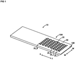
- Figure 1 is an isometric view of a circuit board which is an embodiment of the invention.
- Figure 2 is a top view (A), a side view (B), and a bottom view (C) of the circuit board the isometric view of which is illustrated in Figure 1 .
- circuit board 10 many pads 20 are arranged on both its front surface (see Figure 2 (A) and rear surface (see Figure 2 (C) ). Thus, when the pads 20 are formed on both the front surface and the rear surface of the circuit board 10, more pads 20 can be positioned, as compared with when pads 20 are formed on only one of the surfaces. If the number of pads 20 is the same, the circuit board 10 can be miniaturized. Simply positioning pads on opposite sides of the circuit board leads to the possibility of miniaturization.
- Each of the many pads 20 illustrated in Figure 1 and Figure 2 is a pad responsible for electrical contact with a mating contact provided in a mating connector not illustrated. That is, a portion, where the pads 20 are arranged, in the circuit board 10 is used as a card edge connector 10A. The entire surface of the circuit board, excluding portions adjacent to or just above the pads 20, of at least the portion used as the card edge connector 10A is covered with a protective film called a resist.
- the card edge connector 10A mates with the mating connector by being inserted into the mating connector in a direction indicated by an arrow F.
- the mating connector includes the same number of mating contacts as that of the pads 20 in the same arrangement as that of the pads 20 on the circuit board 10. With the card edge connector 10A completely mated with the mating connector, the mating contacts respectively remain contacting the arranged pads 20.
- a plurality of rows (13 rows in the example herein illustrated) of pads 20 are arranged in a width direction indicated by an arrow W.
- a plurality of pads 20 (eight in the example herein illustrated) are sequentially arranged with spacing in a direction indicated by an arrow F - R in each of the rows.
- the card edge connector 10A is inserted into the mating connector in the direction indicated by the arrow F.
- the mating contact which contacts the pad 20_8 positioned in a rearmost part of the row at the time of complete mating, repeatedly contacts the pads 20, as described below, as the mating progresses. That is, the mating contact that contacts the pad 20_8 slides toward the rear indicated by an arrow R on a protective film 30, and first passes on or over the pad 20_1 while contacting the foremost pad 20_1. The mating contact separates from the pad 20_1 and slides on the protective film 30 again. Then, the mating contact passes on or over the second pad 20_2 from the front while contacting the pad 20_2.
- the mating contact that contacts the second pad 20_2 from the front at the time of complete mating slides on the protective film 30 later than the mating contact that contacts any one of the third and subsequent pads 20_3, ..., 20_8 from the front, and passes on the foremost pad 20_1 while contacting the pad 20_1. Then, the mating contact separates from the pad 20_1 and slides on the protective film 30 again. At the time of complete mating, the mating contact contacts the second pad 20_2 from the front.
- the mating contact corresponding to the pad 20_n positioned at the rear indicated by the arrow R sequentially contacts the pads 20_1 to 20_n-1 positioned in front of the pad 20_n and then contacts the corresponding pad 20_n.
- a trajectory reverse to that at the time of mating takes place. That is, the mating contact corresponding to the pad 20_n positioned at the rear indicated by the arrow R is extracted while sequentially contacting the pads 20_n-1 to 20_1 positioned in front of the pad 20_n.
- Figure 3 shows: (i) an enlarged view R1 of a portion of the circuit board shown in Fig 2A indicated by a dashed circle R1; and (ii) an enlarged sectional view R2 of a portion of the circuit board shown in Fig 2B indicated by a dashed circle R2.
- Figure 2 (B) is a side view of the circuit board
- Figure 3 (R2) is a cross sectional view of the circled portion R2.
- each pad 20 in the present embodiment has a substantially rectangular shape.
- An edge 20a, at a front end in the sliding direction indicated by the arrow F, of each of the pads 20 linearly extends in the width direction indicated by the arrow W.
- the protective film 30 contacts the edge of each of the pads 20 over its circumference without a gap being formed between the edge and the protective film, and spreads to a surface (both a front surface and a rear surface) of a plate-shaped base body 40.
- the two pads 20 adjacent to each other in the sliding direction indicated by the arrow F e.g., the first pad 20_1 and the second pad 20_2 illustrated in Figure 3 , are paid attention to as a specific example.
- the protective film 30 spreads while contacting the edge of each of the pads 20 around its circumference. Accordingly, the protective film 30 contacts both an edge 20b at a rear end of the first pad 20_1 and an edge 20a at a front end of the second pad 20_2, and spreads on or extend over the base body 40.
- this structure As a result of this structure, damage to the mating contact due to introduction and extraction, resulting in the mating contact riding over one or more of the pads 20 is suppressed.
- this structure is repeated for the eight pads 20 arranged in the sliding direction and the protective film 30 that fills spaces between the pads 20, illustrated in Figure 1 or Figure 2 . Therefore, in the present embodiment, damage to the mating contact due to introduction and extraction of the card edge connector into and from the mating connector is suppressed.
- the following processes for example, may be adopted.
- a protective film material is applied to cover the entire surface of the base body 40 on which the pads 20 are formed and/or the edges of each of the pads 20.
- buffing is performed to finish a surface of the protective film material such that it becomes flat. Accordingly, the protective film 30 can be formed, which contacts the edges of each of the pads 20 without a gap being formed between the edges of the pads 20 and the protective film.
- a front end portion 10B on the side, on which the mating contact moves rearward in the sliding direction (in the direction indicated by the arrow R) and first contacts the protective film 30, of the base body 40 has a tapered shape that decreases in thickness toward the front (in the direction indicated by the arrow F) in the present embodiment.
- the protective film 30 covers the front end portion 10B.
- the front end portion 10B or leading end of the base body 40 has a tapered shape.
- mating with the mating connector becomes smooth, and damage to the mating contact and the circuit board is suppressed, reduced or avoided.
- the protective film 30 has a lower friction coefficient than that of the surface of the base body 40.
- the protective film 30 having a low friction coefficient is used so that smooth introduction and extraction with respect to the mating connector are achieved.
- the material forming the protective film 30, may be resin having a low friction coefficient or a glass-based coating agent, for example such a material can be used in addition to a resist generally used to protect the surface of the circuit board.
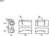
- Figure 4 is a diagram illustrating measured height distribution of the surface of the circuit board.
- Figure 4 (A) illustrates a comparative example to be compared with the invention
- Figure 4 (B) illustrates an example of the invention.
- a groove 50 in which the base body 40 (see Figure 3 (R2)) is almost exposed, exists between the pad 20 and the protective film 30 on the circuit board 10, as indicated in section P of Fig 4 (A) at the upper left corner of Figure 4 .
- the base body 40 is covered with the protective film 30, the pad 20 having been conventionally covered with a slightly larger mask than the pad 20, and is coated with a material for the protective film 30 so as to leave exposed the entire area of the pad 20 from the protective film 30, as illustrated in Figure 4 (A) .
- the protective film 30 is slightly spaced apart from the edges of the pad 20, and the groove 50 is formed between the pad 20 and the protective film 30.
- the shape of the pad 20 is a shape tapered in the sliding direction.
- the protective film 30 on the circuit board 10 contacts the edges of the pad 20, and no grooves exist therebetween, as indicated by section P of Fig 4 (B) at the lower left of Figure 4 .
- the pad 20 is covered with a slightly smaller mask than the pad 20, and is coated with a material for the protective film 30, for example, as described above. Accordingly, a protective film 30 that overlaps even the edges of the pad 20 is formed. Then, buffing is performed such that a surface of the protective film 30 becomes flat.
- each pad 20 has a substantially rectangular shape, and edges extending in the width direction are formed.
- Figure 4 (X) is a diagram illustrating a height distribution of the surface of the circuit board 10 along a broken line X transversely extending for each of the examples (A) and (B) in section P of Figure 4 .
- Figure 4 (Y) is a diagram illustrating a height distribution of the surface of the circuit board 10 along a broken line Y longitudinally extending for each of the examples (A) and (B) in section P of Figure 4 .
- the card edge connector 10A in or on which the plurality of pads 20 are arranged in a two-dimensional manner, as illustrated in Figure 1 and Figure 2 has been shown and described. Note that the invention is also applicable to a card edge connector of such a type that pads 20 are arranged in only one row in a width direction.
- the invention is not limited to card edge connectors.
- the invention is also applicable to a circuit board of such a type that a mating contact arranged in a two-dimensional manner approaches a circuit board from above and is pressed against pads arranged in a two-dimensional manner on the circuit board while being slid slightly
Landscapes
- Engineering & Computer Science (AREA)
- Microelectronics & Electronic Packaging (AREA)
- Manufacturing & Machinery (AREA)
- Printing Elements For Providing Electric Connections Between Printed Circuits (AREA)
- Coupling Device And Connection With Printed Circuit (AREA)
- Non-Metallic Protective Coatings For Printed Circuits (AREA)
- Structure Of Printed Boards (AREA)
Abstract
Description
- The present invention relates to a circuit board appropriate for a card edge connector.
- A card edge connector using an electrically conductive pad formed in a circuit board as a contact that electrically contacts a mating contact provided in a connector as a mating counterpart is known.
- For example,
JP3894774B - A protective film called a resist is often formed in a circuit board. A pad responsible for electrical conduction is often formed in or on the circuit board. For example, in the case of a card edge connector, a pad responsible for electrical contact with a mating contact provided in a connector as a mating counterpart is formed. In forming the protective film in or on the circuit board where the pad is formed, a portion of the pad is masked to be slightly wide such that the pad is not covered with the protective film, and is then coated with a resist liquid. Accordingly, a gap is formed between an edge of the pad and the protective film. In the case of the card edge connector, in mating with the mating connector, the mating contact slides on the protective film in or on the circuit board and rides over the pad so that the pad and the mating contact contact each other. Accordingly, in attachment to and detachment from the mating connector, the mating contact and the circuit board may be damaged by each other without the mating contact smoothly sliding onto the pad from the protective film or onto the protective film from the pad due to the presence of the above-described gap. That is, when the attachment and detachment are repeated, deterioration of the mating contact and the circuit board may occur.
- In the case of the card edge connector disclosed in the above-mentioned
JP3894774B - The present invention has as its object to provide a circuit board that includes a protective film, is of such a type that a mating contact slides on the protective film and rides over the pad, and is prevented from deteriorating due to attachment and detachment of the mating contact.
- A circuit board according to the invention to attain the above-described object includes a plate-shaped base body, at least one pad formed on a surface of the base body and responsible for electrical contact with a mating contact, and a protective film spreading or disposed on the surface of the base body in contact with an edge of the pad.
- In the circuit board according to the invention, the protective film spreads or is in contact with the edge of the pad, whereby deterioration due to attachment and detachment of a mating contact is reduced compared with a circuit board of the type in which a gap is formed between a protective film and an edge of a pad.
- In the circuit board according to the invention, the edge of the pad and a portion of the protective film, which contacts the edge of the pad, preferably respectively have the same or substantially the same heights with respect to each other.
- When the edge of the pad and the portion of the protective film, which contacts the edge of the pad, have the same height, the deterioration of the mating contact and the pad, due to attachment and detachment, is further reduced.
- In the circuit board according to the invention, it is preferable that the pad contacts, by causing the mating contact that has slid rearward in a predetermined sliding direction in contact with the protective film to ride over the pad, the mating contact that has ridden over the pad, and an edge, at a front end in the sliding direction, of the pad linearly extends in a width direction intersecting the sliding direction.
- When the edge, at the front end in the sliding direction, of the pad is pointed forward, the mating contact contacts the pointed front end having a narrow width in riding over the pad, whereby the mating contact is easily damaged. On the other hand, when the edge at the front end of the pad linearly extends in the width direction intersecting the sliding direction, the damage is more suppressed, as compared with when the edge at the front end of the pad is pointed forward.
- In the circuit board according to the invention, it is preferable that the plurality of pads are sequentially arranged with spacing in the sliding direction, and the protective film spreads on the surface of the base body in contact with both an edge at a rear end of the first pad positioned relatively in front among the plurality of pads arranged in the sliding direction and an edge at a front end of the second pad adjacent to the rear of the first pad.
- In the case of this structure, the damage is suppressed even in both introduction and extraction from a state where the mating contact rides over the first pad or the second pad until a state where the mating contact rides over the other pad.
- In the circuit board according to the invention, it is preferable that a plurality of rows each including the plurality of pads sequentially arranged with spacing in the sliding direction are arranged in a width direction intersecting the sliding direction, and the pads arranged in the two rows adjacent to each other in the width direction are respectively formed at positions deviating from each other in the sliding direction.
- When the pads are respectively formed at the positions deviating from each other in the sliding direction, the pads can be more closely positioned in the width direction, as compared with when the pads are formed at the same position in the sliding direction. Therefore, this contributes to miniaturization of the circuit board.
- In the circuit board according to the invention, both the pad and the protective film are preferably respectively formed on both surfaces of the base body.
- When the pad and the protective film are respectively formed on both surfaces of the base body, miniaturization of the circuit board is achieved.
- Further, in the circuit board according to the invention, it is preferable that a front end portion on the side, on which the mating contact moves rearward in the sliding direction and first contacts the protective film, of the base body has a tapered shape that decreases in thickness toward the front, and the protective film covers the front end portion and spreads.
- When the front end portion has a tapered shape, and the front end portion is covered with the protective film, mating with the mating connector is smoothed, and a damage to the front end portion or the mating contact is suppressed.
- Further, in the circuit board according to the invention, the protective film preferably has a lower friction coefficient than that of the surface of the base body. When the protective film having a low friction coefficient is formed, smooth introduction and extraction are performed.
- In the above-described circuit board according to the invention, deterioration due to attachment and detachment of a mating contact (damage to the mating contact and/or the circuit board) is suppressed or reduced.
-
-
Figure 1 is an isometric view of a circuit board according to an embodiment of the invention. -
Figure 2 is a top view (A), a side view (B), and a bottom view (C) of the circuit board, the isometric view of which is illustrated inFigure 1 . -
Figure 3 shows: (i) an enlarged view R1 of a portion of the circuit board shown inFig 2A indicated by a dashed circle R1; and (ii) an enlarged sectional view R2 of a portion of the circuit board shown inFig 2B indicated by a dashed circle R2. -
Figure 4 is a diagram illustrating measured height distribution of the surface of the circuit board. - An embodiment of the invention will be described below.
-
Figure 1 is an isometric view of a circuit board which is an embodiment of the invention. -
Figure 2 is a top view (A), a side view (B), and a bottom view (C) of the circuit board the isometric view of which is illustrated inFigure 1 . - In
Figure 1 andFigure 2 , illustration of elements of the circuit board other than elements characteristic of the present embodiment have been omitted. Description of the elements which have been omitted has also been omitted. - In the
circuit board 10,many pads 20 are arranged on both its front surface (seeFigure 2 (A) and rear surface (seeFigure 2 (C) ). Thus, when thepads 20 are formed on both the front surface and the rear surface of thecircuit board 10,more pads 20 can be positioned, as compared with whenpads 20 are formed on only one of the surfaces. If the number ofpads 20 is the same, thecircuit board 10 can be miniaturized. Simply positioning pads on opposite sides of the circuit board leads to the possibility of miniaturization. - Each of the
many pads 20 illustrated inFigure 1 andFigure 2 is a pad responsible for electrical contact with a mating contact provided in a mating connector not illustrated. That is, a portion, where thepads 20 are arranged, in thecircuit board 10 is used as acard edge connector 10A. The entire surface of the circuit board, excluding portions adjacent to or just above thepads 20, of at least the portion used as thecard edge connector 10A is covered with a protective film called a resist. - The
card edge connector 10A mates with the mating connector by being inserted into the mating connector in a direction indicated by an arrow F. The mating connector includes the same number of mating contacts as that of thepads 20 in the same arrangement as that of thepads 20 on thecircuit board 10. With thecard edge connector 10A completely mated with the mating connector, the mating contacts respectively remain contacting the arrangedpads 20. - Here, the arrangement of the
pads 20 on thecircuit board 10 will be described. - A plurality of rows (13 rows in the example herein illustrated) of
pads 20 are arranged in a width direction indicated by an arrow W. A plurality of pads 20 (eight in the example herein illustrated) are sequentially arranged with spacing in a direction indicated by an arrow F - R in each of the rows. - In mating with the mating connector, the
card edge connector 10A is inserted into the mating connector in the direction indicated by the arrow F. At this time, for example, the mating contact, which contacts the pad 20_8 positioned in a rearmost part of the row at the time of complete mating, repeatedly contacts thepads 20, as described below, as the mating progresses. That is, the mating contact that contacts the pad 20_8 slides toward the rear indicated by an arrow R on aprotective film 30, and first passes on or over the pad 20_1 while contacting the foremost pad 20_1. The mating contact separates from the pad 20_1 and slides on theprotective film 30 again. Then, the mating contact passes on or over the second pad 20_2 from the front while contacting the pad 20_2. This is repeated until the mating contact finally contacts the pad 20_8 positioned in the rearmost part of the row. For example, the mating contact that contacts the second pad 20_2 from the front at the time of complete mating slides on theprotective film 30 later than the mating contact that contacts any one of the third and subsequent pads 20_3, ..., 20_8 from the front, and passes on the foremost pad 20_1 while contacting the pad 20_1. Then, the mating contact separates from the pad 20_1 and slides on theprotective film 30 again. At the time of complete mating, the mating contact contacts the second pad 20_2 from the front. Thus, the mating contact corresponding to the pad 20_n positioned at the rear indicated by the arrow R sequentially contacts the pads 20_1 to 20_n-1 positioned in front of the pad 20_n and then contacts the corresponding pad 20_n. When thecard edge connector 10A is extracted from the mating connector, a trajectory reverse to that at the time of mating takes place. That is, the mating contact corresponding to the pad 20_n positioned at the rear indicated by the arrow R is extracted while sequentially contacting the pads 20_n-1 to 20_1 positioned in front of the pad 20_n. - When an arrangement of the plurality of pads 20 (eight in the example herein illustrated) arranged in the direction indicated by the arrow F - R is taken as one row, a plurality of rows (13 rows in the example herein illustrated) are arranged in the width direction indicated by the arrow W. The
pads 20 respectively belonging to the rows adjacent to each other in the width direction are respectively positioned at positions deviating from each other in a sliding direction indicated by the arrow F - R. When thepads 20 are thus respectively formed at the deviating positions, a region where nopad 20 exists more spreads around each of thepads 20, as compared with when thepads 20 are formed at the same position in the sliding direction. When the region where nopad 20 exists spreads, each of thepads 20 is not easily electrically affected by theadjacent pad 20. In other words, thepads 20 of each row are staggered with respect to those in any adjacent row. As a result, thepads 20 can be closely positioned in the width direction. Thus, miniaturization of the circuit board is realized. -
Figure 3 shows: (i) an enlarged view R1 of a portion of the circuit board shown inFig 2A indicated by a dashed circle R1; and (ii) an enlarged sectional view R2 of a portion of the circuit board shown inFig 2B indicated by a dashed circle R2. AlthoughFigure 2 (B) is a side view of the circuit board,Figure 3 (R2) is a cross sectional view of the circled portion R2. - As illustrated in
Figure 3 (R1), eachpad 20 in the present embodiment has a substantially rectangular shape. Anedge 20a, at a front end in the sliding direction indicated by the arrow F, of each of thepads 20 linearly extends in the width direction indicated by the arrow W. - When the edge at the front end in the sliding direction of the pad is pointed forward, the mating contact that has slid contacts the pointed front end having a narrow width in riding over the
pad 20, whereby the mating contact is easily damaged. On the other hand, when the edge at the front end of thepad 20 linearly extends in the width direction intersecting the sliding direction, as in the present embodiment, damage is more suppressed, as compared with when the edge at the front end of the pad is pointed forward. - The
protective film 30 contacts the edge of each of thepads 20 over its circumference without a gap being formed between the edge and the protective film, and spreads to a surface (both a front surface and a rear surface) of a plate-shapedbase body 40. Here, the twopads 20 adjacent to each other in the sliding direction indicated by the arrow F, e.g., the first pad 20_1 and the second pad 20_2 illustrated inFigure 3 , are paid attention to as a specific example. Theprotective film 30 spreads while contacting the edge of each of thepads 20 around its circumference. Accordingly, theprotective film 30 contacts both anedge 20b at a rear end of the first pad 20_1 and anedge 20a at a front end of the second pad 20_2, and spreads on or extend over thebase body 40. As a result of this structure, damage to the mating contact due to introduction and extraction, resulting in the mating contact riding over one or more of thepads 20 is suppressed. In the present embodiment, this structure is repeated for the eightpads 20 arranged in the sliding direction and theprotective film 30 that fills spaces between thepads 20, illustrated inFigure 1 orFigure 2 . Therefore, in the present embodiment, damage to the mating contact due to introduction and extraction of the card edge connector into and from the mating connector is suppressed. - To form the
protective film 30 that contacts the edges of each of thepads 20 without a gap being formed between the edges of thepad 20 and the film, the following processes, for example, may be adopted. A protective film material is applied to cover the entire surface of thebase body 40 on which thepads 20 are formed and/or the edges of each of thepads 20. Then, buffing is performed to finish a surface of the protective film material such that it becomes flat. Accordingly, theprotective film 30 can be formed, which contacts the edges of each of thepads 20 without a gap being formed between the edges of thepads 20 and the protective film. - For the
base body 40, afront end portion 10B on the side, on which the mating contact moves rearward in the sliding direction (in the direction indicated by the arrow R) and first contacts theprotective film 30, of thebase body 40 has a tapered shape that decreases in thickness toward the front (in the direction indicated by the arrow F) in the present embodiment. Theprotective film 30 covers thefront end portion 10B. - Thus, the
front end portion 10B or leading end of thebase body 40 has a tapered shape. When thefront end portion 10B is covered with theprotective film 30, mating with the mating connector becomes smooth, and damage to the mating contact and the circuit board is suppressed, reduced or avoided. - Further, in the present embodiment, the
protective film 30 has a lower friction coefficient than that of the surface of thebase body 40. Theprotective film 30 having a low friction coefficient is used so that smooth introduction and extraction with respect to the mating connector are achieved. - The material forming the
protective film 30, may be resin having a low friction coefficient or a glass-based coating agent, for example such a material can be used in addition to a resist generally used to protect the surface of the circuit board. -
Figure 4 is a diagram illustrating measured height distribution of the surface of the circuit board.Figure 4 (A) illustrates a comparative example to be compared with the invention, andFigure 4 (B) illustrates an example of the invention. - In the comparative example illustrated in
Figure 4 (A) agroove 50, in which the base body 40 (seeFigure 3 (R2)) is almost exposed, exists between thepad 20 and theprotective film 30 on thecircuit board 10, as indicated in section P ofFig 4 (A) at the upper left corner ofFigure 4 . This will be the case if thebase body 40 is covered with theprotective film 30, thepad 20 having been conventionally covered with a slightly larger mask than thepad 20, and is coated with a material for theprotective film 30 so as to leave exposed the entire area of thepad 20 from theprotective film 30, as illustrated inFigure 4 (A) . Accordingly, theprotective film 30 is slightly spaced apart from the edges of thepad 20, and thegroove 50 is formed between thepad 20 and theprotective film 30. The shape of thepad 20 is a shape tapered in the sliding direction. - On the other hand, in the example illustrated in
Figure 4 (B) , theprotective film 30 on thecircuit board 10 contacts the edges of thepad 20, and no grooves exist therebetween, as indicated by section P ofFig 4 (B) at the lower left ofFigure 4 . To form this structure, thepad 20 is covered with a slightly smaller mask than thepad 20, and is coated with a material for theprotective film 30, for example, as described above. Accordingly, aprotective film 30 that overlaps even the edges of thepad 20 is formed. Then, buffing is performed such that a surface of theprotective film 30 becomes flat. As a result, a portion, which overlaps the edges of thepad 20, of theprotective film 30 is scraped or buffed off, thepad 20 is exposed to its edges, and theprotective film 30 that extends into contact with the edges is formed. In the present embodiment, eachpad 20 has a substantially rectangular shape, and edges extending in the width direction are formed. -
Figure 4 (X) is a diagram illustrating a height distribution of the surface of thecircuit board 10 along a broken line X transversely extending for each of the examples (A) and (B) in section P ofFigure 4 . -
Figure 4 (Y) is a diagram illustrating a height distribution of the surface of thecircuit board 10 along a broken line Y longitudinally extending for each of the examples (A) and (B) in section P ofFigure 4 . - As can be seen from the drawings, in the comparative example illustrated in
Figure 4 (A) , adeep groove 50 is formed. Accordingly, when the mating connector that has slid passes through or over thegroove 50, thecircuit board 10 is damaged. When this is repeated, there may occur such malfunctions that the surface of thecircuit board 10 is scraped off and the edge of thepad 20 is rolled up, for example (in turn, also including malfunctions such as damage to and wear of the mating contact that slides over the pad). On the other hand, in the example illustrated inFigure 4 (B) , nogroove 50 is formed, and the edge of thepad 20 and a portion, which contacts the edge of thepad 20, of theprotective film 30 respectively have the same height as each other. Accordingly, even if the mating contact moves across thepad 20 and theprotective film 30, damage to the mating contact or damage to thecircuit board 10 may be slight or non-existent. Accordingly, in the present embodiment, a circuit board having a high reliability in which the possibility of occurrence of the above-described malfunctions has been suppressed is realized. - Here, the
card edge connector 10A in or on which the plurality ofpads 20 are arranged in a two-dimensional manner, as illustrated inFigure 1 andFigure 2 has been shown and described. Note that the invention is also applicable to a card edge connector of such a type thatpads 20 are arranged in only one row in a width direction. - The invention is not limited to card edge connectors. For example, the invention is also applicable to a circuit board of such a type that a mating contact arranged in a two-dimensional manner approaches a circuit board from above and is pressed against pads arranged in a two-dimensional manner on the circuit board while being slid slightly
-
- 10a...
- circuit board
- 10A
- card edge connector
- 10B
- front end portion or leading portion
- 20, 20_1, .., 20_8
- pad
- 20a
- edge at front end of pad
- 20b
- edge at rear end of pad
- 30
- protective film
- 40
- base body
- 50
- groove
Claims (10)
- A circuit board (10), comprising:
a plate-shaped base body (40):at least one pad (20) formed on a surface of the base body (40) and configured for electrical contact with a mating contact; anda protective film (30) in contact with an edge (20a, 20b) of the pad (20) and extending over the surface of the base body (40). - The circuit board (10) according to claim 1, wherein the edge (20a, 20b) of the pad (20) and a portion of the protective film (30) that is in contact with the edge (20a, 20b) respectively have the same height as each other and/or form a continuous upper surface.
- The circuit board (10) according to claim 1 or 2, wherein the pad (20) is adapted to cause the mating contact sliding rearward in a predetermined sliding direction (RF) in contact with the protective film (30) to ride over the pad (20) and to contact the pad (20) that is ridden over, and an edge (20a) of the pad (20) at a front end thereof in the sliding direction extends linearly in a width direction (W) intersecting the sliding direction (RF).
- The circuit board (10) according to any one of claims 1 to 3, wherein a plurality of said pads (20) are sequentially arranged with spacing in a sliding direction (RF), and the protective film (30) is in contact with both an edge (20b) at a rear end of a first pad (20_1) positioned relatively in front among the plurality of pads (20) arranged in the sliding direction (RF) and an edge (20a) at a front end of a second said pad (20_2) adjacent to the rear of the first pad (20_1) and extends over the surface of the base body (40).
- The circuit board (10) according to any one of claims 1 to 4, wherein a plurality of rows, each including a plurality of said pads (20) sequentially arranged with spacing in a sliding direction (RF), are arranged in a width direction (W) intersecting the sliding direction (RF), and the pads (20) arranged in two said rows adjacent to each other in the width direction (W) are respectively formed at positions deviating from each other in the sliding direction (RF).
- The circuit board (10) according to any one of claims 1 to 5, wherein at least one said pad (20) and one said protective film (30) are formed on both said surface and an oppositely facing surface of the base body (40).
- The circuit board (10) according to any one of claims 1 to 6, wherein a front end portion (10B) on the side of the base body on which the mating contact moves rearward in the sliding direction (RF) and first contacts (40) the protective film (30), has a tapered shape that decreases in thickness toward a front of the circuit board (10), and the protective film (30) covers the front end portion (10B) and spreads.
- The circuit board (10) according to any one of claims 1 to 6 wherein a leading front end portion (10B) of the circuit board (10), configured to be engaged by a mating connector including the mating contact, is tapered and covered by the protection film (30).
- The circuit board according to any one of claims 1 to 8, wherein the protective film has a lower friction coefficient than that of the surface of the base body.
- A method of forming a circuit board including the steps of:(i) forming a circuit board (10) with contact pads (20) on a surface of a base body (40);(ii) applying a protective film material (30) so as to entirely cover the surface of the base body (40) on which the pads are formed; and(iii) removing part of the protective film material (30) such that an exposed surface of the protective film material (30) becomes flat and the contact pads (20) are exposed.
Applications Claiming Priority (1)
| Application Number | Priority Date | Filing Date | Title |
|---|---|---|---|
| JP2020136680A JP7666861B2 (en) | 2020-08-13 | 2020-08-13 | Circuit Board |
Publications (1)
| Publication Number | Publication Date |
|---|---|
| EP3955709A1 true EP3955709A1 (en) | 2022-02-16 |
Family
ID=77274694
Family Applications (1)
| Application Number | Title | Priority Date | Filing Date |
|---|---|---|---|
| EP21190478.4A Pending EP3955709A1 (en) | 2020-08-13 | 2021-08-10 | Circuit board and method of forming the same |
Country Status (5)
| Country | Link |
|---|---|
| US (1) | US11602049B2 (en) |
| EP (1) | EP3955709A1 (en) |
| JP (1) | JP7666861B2 (en) |
| CN (1) | CN114080102A (en) |
| CA (1) | CA3127775C (en) |
Families Citing this family (1)
| Publication number | Priority date | Publication date | Assignee | Title |
|---|---|---|---|---|
| KR102857721B1 (en) * | 2024-07-29 | 2025-09-10 | 주식회사 티에스이 | Burn-in socket |
Citations (5)
| Publication number | Priority date | Publication date | Assignee | Title |
|---|---|---|---|---|
| US4298237A (en) * | 1979-12-20 | 1981-11-03 | Bell Telephone Laboratories, Incorporated | Printed wiring board interconnection apparatus |
| JP3894774B2 (en) | 2001-10-31 | 2007-03-22 | 富士通株式会社 | Card edge connector and method for manufacturing the same, electronic card and electronic device |
| US20080089041A1 (en) * | 2001-07-30 | 2008-04-17 | Seiko Epson Corporation | Connection apparatus for circuit board, ink jet type recording apparatus using the same, ic chip and ink cartridge having ic chip |
| WO2009025059A1 (en) * | 2007-08-23 | 2009-02-26 | Fujitsu Limited | Printed board and method for producing the same |
| US20160249454A1 (en) * | 2010-04-28 | 2016-08-25 | International Business Machines Corporation | Printed Circuit Board Edge Connector |
Family Cites Families (11)
| Publication number | Priority date | Publication date | Assignee | Title |
|---|---|---|---|---|
| JPS49139552U (en) | 1973-03-31 | 1974-12-02 | ||
| JPH0186264U (en) * | 1987-11-28 | 1989-06-07 | ||
| JP5146234B2 (en) * | 2008-09-30 | 2013-02-20 | 富士通株式会社 | Function expansion device, method of manufacturing the same, and electronic device system |
| JP2011009363A (en) * | 2009-06-24 | 2011-01-13 | Nec Corp | Semiconductor device, method of manufacturing the same, and composite circuit device using the same |
| JP2013106032A (en) * | 2011-11-14 | 2013-05-30 | Sda Co Ltd | Clearance filling pcb and method of manufacturing the same |
| CN105453192B (en) * | 2013-08-07 | 2018-05-18 | 松下知识产权经营株式会社 | Resistor and manufacturing method thereof |
| JP5941446B2 (en) * | 2013-09-05 | 2016-06-29 | 株式会社フジクラ | Printed wiring board and connector for connecting the wiring board |
| KR102537545B1 (en) * | 2016-05-10 | 2023-05-30 | 삼성디스플레이 주식회사 | Printed circuit board and display apparatus including the same |
| KR102555729B1 (en) * | 2016-07-15 | 2023-07-17 | 삼성디스플레이 주식회사 | Flexible film, circuit board assembly and display apparatus |
| US10916903B2 (en) * | 2018-02-04 | 2021-02-09 | Creganna Unlimited Company | System having a cable assembly and plug and receptacle connectors |
| JP2020101616A (en) * | 2018-12-20 | 2020-07-02 | 日本電気硝子株式会社 | Electronic device manufacturing method and glass substrate |
-
2020
- 2020-08-13 JP JP2020136680A patent/JP7666861B2/en active Active
-
2021
- 2021-08-09 US US17/397,382 patent/US11602049B2/en active Active
- 2021-08-10 EP EP21190478.4A patent/EP3955709A1/en active Pending
- 2021-08-10 CA CA3127775A patent/CA3127775C/en active Active
- 2021-08-11 CN CN202110922270.8A patent/CN114080102A/en active Pending
Patent Citations (5)
| Publication number | Priority date | Publication date | Assignee | Title |
|---|---|---|---|---|
| US4298237A (en) * | 1979-12-20 | 1981-11-03 | Bell Telephone Laboratories, Incorporated | Printed wiring board interconnection apparatus |
| US20080089041A1 (en) * | 2001-07-30 | 2008-04-17 | Seiko Epson Corporation | Connection apparatus for circuit board, ink jet type recording apparatus using the same, ic chip and ink cartridge having ic chip |
| JP3894774B2 (en) | 2001-10-31 | 2007-03-22 | 富士通株式会社 | Card edge connector and method for manufacturing the same, electronic card and electronic device |
| WO2009025059A1 (en) * | 2007-08-23 | 2009-02-26 | Fujitsu Limited | Printed board and method for producing the same |
| US20160249454A1 (en) * | 2010-04-28 | 2016-08-25 | International Business Machines Corporation | Printed Circuit Board Edge Connector |
Also Published As
| Publication number | Publication date |
|---|---|
| US20220053642A1 (en) | 2022-02-17 |
| US11602049B2 (en) | 2023-03-07 |
| CA3127775A1 (en) | 2022-02-13 |
| JP7666861B2 (en) | 2025-04-22 |
| CN114080102A (en) | 2022-02-22 |
| CA3127775C (en) | 2023-11-07 |
| JP2022032666A (en) | 2022-02-25 |
Similar Documents
| Publication | Publication Date | Title |
|---|---|---|
| US5199886A (en) | Shrouded connector assembly | |
| DE69326576T2 (en) | Shielded electrical connector | |
| US6780058B2 (en) | Shielded backplane connector | |
| US7883366B2 (en) | High density connector assembly | |
| US3411127A (en) | Self-mating electric connector assembly | |
| US9246283B2 (en) | Connector terminal and electrical connector | |
| US8727791B2 (en) | Electrical connector assembly | |
| DE3586439T2 (en) | ELECTRICAL CONNECTOR AND METHOD FOR PRODUCING THE SAME. | |
| EP0697755B1 (en) | Electrical connector for printed circuit boards | |
| EP0036264B1 (en) | An electrical terminal and a zero insertion force electrical connector comprising such terminals | |
| US20150132998A1 (en) | Electrical Connector | |
| US20040259419A1 (en) | Electrical connector with multi-beam contact | |
| US5037334A (en) | Connector with equal lateral force contact spacer plate | |
| US3395377A (en) | Digital connector | |
| DE68918547T2 (en) | Electrical connector system. | |
| EP3955709A1 (en) | Circuit board and method of forming the same | |
| JPH0636834A (en) | Memory card connector device | |
| WO2015105680A1 (en) | Electrical connector having compliant contacts and a circuit board assembly including the same | |
| US6843688B2 (en) | Connector in which movement of contact portion of contact is guided by insulator | |
| US6984137B2 (en) | Electrical connector and electrical connector assembly | |
| DE60310303T2 (en) | PCB edge connector and card | |
| EP1158619A2 (en) | Electrical connector capable of exerting a selectively variable contact force | |
| US3763462A (en) | Control wipe electrical connector for circuit cards | |
| DE60318465T2 (en) | MEMORY CARD CONNECTOR | |
| JP3251079B2 (en) | Terminal part for FPC connector |
Legal Events
| Date | Code | Title | Description |
|---|---|---|---|
| PUAI | Public reference made under article 153(3) epc to a published international application that has entered the european phase |
Free format text: ORIGINAL CODE: 0009012 |
|
| STAA | Information on the status of an ep patent application or granted ep patent |
Free format text: STATUS: THE APPLICATION HAS BEEN PUBLISHED |
|
| AK | Designated contracting states |
Kind code of ref document: A1 Designated state(s): AL AT BE BG CH CY CZ DE DK EE ES FI FR GB GR HR HU IE IS IT LI LT LU LV MC MK MT NL NO PL PT RO RS SE SI SK SM TR |
|
| STAA | Information on the status of an ep patent application or granted ep patent |
Free format text: STATUS: REQUEST FOR EXAMINATION WAS MADE |
|
| 17P | Request for examination filed |
Effective date: 20220803 |
|
| RBV | Designated contracting states (corrected) |
Designated state(s): AL AT BE BG CH CY CZ DE DK EE ES FI FR GB GR HR HU IE IS IT LI LT LU LV MC MK MT NL NO PL PT RO RS SE SI SK SM TR |
|
| RAP3 | Party data changed (applicant data changed or rights of an application transferred) |
Owner name: TE CONNECTIVITY JAPAN G.K. |