EP3955296A1 - Semiconductor structure and method for forming same - Google Patents
Semiconductor structure and method for forming same Download PDFInfo
- Publication number
- EP3955296A1 EP3955296A1 EP21798541.5A EP21798541A EP3955296A1 EP 3955296 A1 EP3955296 A1 EP 3955296A1 EP 21798541 A EP21798541 A EP 21798541A EP 3955296 A1 EP3955296 A1 EP 3955296A1
- Authority
- EP
- European Patent Office
- Prior art keywords
- word lines
- trenches
- forming
- semiconductor structure
- areas
- Prior art date
- Legal status (The legal status is an assumption and is not a legal conclusion. Google has not performed a legal analysis and makes no representation as to the accuracy of the status listed.)
- Granted
Links
Images







Classifications
-
- H—ELECTRICITY
- H10—SEMICONDUCTOR DEVICES; ELECTRIC SOLID-STATE DEVICES NOT OTHERWISE PROVIDED FOR
- H10B—ELECTRONIC MEMORY DEVICES
- H10B12/00—Dynamic random access memory [DRAM] devices
- H10B12/01—Manufacture or treatment
- H10B12/02—Manufacture or treatment for one transistor one-capacitor [1T-1C] memory cells
- H10B12/05—Making the transistor
- H10B12/053—Making the transistor the transistor being at least partially in a trench in the substrate
-
- H—ELECTRICITY
- H10—SEMICONDUCTOR DEVICES; ELECTRIC SOLID-STATE DEVICES NOT OTHERWISE PROVIDED FOR
- H10B—ELECTRONIC MEMORY DEVICES
- H10B12/00—Dynamic random access memory [DRAM] devices
- H10B12/30—DRAM devices comprising one-transistor - one-capacitor [1T-1C] memory cells
- H10B12/34—DRAM devices comprising one-transistor - one-capacitor [1T-1C] memory cells the transistor being at least partially in a trench in the substrate
-
- H—ELECTRICITY
- H10—SEMICONDUCTOR DEVICES; ELECTRIC SOLID-STATE DEVICES NOT OTHERWISE PROVIDED FOR
- H10B—ELECTRONIC MEMORY DEVICES
- H10B12/00—Dynamic random access memory [DRAM] devices
- H10B12/30—DRAM devices comprising one-transistor - one-capacitor [1T-1C] memory cells
- H10B12/48—Data lines or contacts therefor
- H10B12/488—Word lines
Definitions
- the disclosure relates to the technical field of semiconductors, in particular, to a semiconductor structure and a method for forming the semiconductor structure.
- Semiconductor devices have been widely used in integrated circuits.
- dynamic random access memories are a type of semiconductor memories widely used in the integrated circuits.
- semiconductor devices With a continuous decrease of characteristic sizes of semiconductor integrated circuit devices, semiconductor devices are also constantly developing towards a high integration density, and therefore, more severe challenges are presented to the semiconductor forming technology.
- the semiconductor devices may generate leakage current, which will affect storage performance thereof.
- the technical problem to be solved by the disclosure is to provide a semiconductor structure and a method for forming the semiconductor structure, which can reduce the leakage current of the semiconductor structure and improve the storage performance of a semiconductor device.
- the present disclosure provides a method for forming a semiconductor structure, the method includes: providing a semiconductor substrate, which has multiple separate active areas that are isolated from each other by shallow trench isolation areas; forming trenches by etching the active areas and the shallow trench isolation areas, herein the trenches include first trenches and second trenches, the first trenches are located in the active areas, the second trenches are located in the shallow trench isolation areas, and the first trenches have a width greater than a width of the second trenches; forming word lines in the trenches, herein the word lines include first word lines and second word lines, each first word line is located in a respective first trench, each second word line is located in a respective second trench, and the first word lines have a width greater than a width of the second word lines.
- an etch rate of an etching substance on the shallow trench isolation areas is less than an etch rate of an etching substance on the active areas, so that the first trenches have the width greater than the width of the second trenches.
- first trenches have a depth less than a depth of the second trenches, and a distance from a bottom of the first word lines to a surface of the semiconductor substrate is less than a distance from a bottom of the second trenches to the surface of the semiconductor substrate.
- the method further includes: forming a sacrificial layer on the surface of the semiconductor substrate, herein the sacrificial layer covers the active areas and the shallow trench isolation areas; and forming the trenches by etching the active areas and the shallow trench isolation areas includes: forming the trenches by etching the sacrificial layer, the active areas, and the shallow trench isolation areas.
- forming the word lines in the trenches further includes: forming a dielectric layer, an adhesion layer, and a conductive layer in the trenches in sequence, herein the dielectric layer covers at least an internal surface of the trenches, the adhesion layer covers at least the dielectric layer, and the conductive layer fills at least the trenches; and forming the word lines by removing part of the adhesion layer and the conductive layer, herein the word lines have an upper surface lower than a surface of the substrate.
- a protective layer is filled, the protective layer covering at least the word lines.
- the present disclosure further provides a semiconductor substrate formed by the above-mentioned method for forming a semiconductor structure.
- the semiconductor structure includes a semiconductor substrate, which has multiple separate active areas that are isolated from each other by shallow trench isolation areas; and word lines, including first word lines and second word lines.
- word lines including first word lines and second word lines.
- the first word lines are located in the active areas
- the second word lines are located in the shallow trench isolation areas
- the first word lines have a width greater than a width of the second word lines.
- a difference between the width of the first word lines and the width of the second word lines ranges from 4nm to 10nm.
- the width of the first word lines ranges from 20nm to 30nm
- the width of the second word lines ranges from 17nm to 25nm.
- a distance from the bottom of the first word lines to the surface of the semiconductor substrate is less than a distance from the bottom of the second word lines to the surface of the semiconductor substrate.
- the distance from the bottom of the first word lines to the surface of the semiconductor substrate ranges from 140nm to 165nm, and the distance from the bottom of the second word lines to the surface of the semiconductor substrate ranges from 175nm to 190nm.
- the upper surface of the word lines is lower than the surface of the semiconductor substrate.
- a distance from the upper surface of the word lines to the surface of the semiconductor substrate ranges from 60nm to 75nm.
- each word line includes a dielectric layer, an adhesion layer, and a conductive layer which are arranged in sequence.
- the adhesion layer has an upper surface lower than an upper surface of the conductive layer.
- the semiconductor structure also includes a protective layer which covers at least the word lines.
- a depth of the first word lines ranges from 65nm to 105nm
- a depth of the second word lines ranges from 100nm to 130nm
- the width of the first word lines ranges from 20nm to 30nm
- the width of the second word lines ranges from 17nm to 25nm.
- the present disclosure has the advantages that for the semiconductor structure formed by the method for forming a semiconductor structure of the present disclosure, if a thickness of each shallow trench isolation area between the respective second word line and the respective adjacent active area is large enough, when the second word lines are powered to work, an inversion layer, on the active areas, induced by the second word lines has a small or no thickness, which is not enough to form a parasitic transistor structure, so that there is no leakage current generated, and the storage performance of the semiconductor device is greatly improved.
- the semiconductor device may generate leakage current.
- a cause of the leakage current is that a parasitic transistor structure is formed in a semiconductor structure.
- the parasitic transistor structure may generate the leakage current in the semiconductor device.
- a buried Word Line may simultaneously pass through an Active Area (AA) and a Shallow Trench Isolation (STI) area; and when working, the buried word line in the shallow trench isolation area may induce an inversion layer on the active area adjacent the shallow trench isolation area so as to form the parasitic transistor structure, thereby generating the leakage current.
- AA Active Area
- STI Shallow Trench Isolation
- the disclosure provides a semiconductor structure and a method for manufacturing the semiconductor structure, which can avoid the formation of the parasitic transistor structure so as to avoid generating the leakage current in the semiconductor structure.
- FIG. 1 is a schematic diagram of steps of a method for forming a semiconductor structure according to an embodiment of the disclosure.
- the method for forming a semiconductor structure includes steps S10 to S12.
- a semiconductor substrate is provided, and the semiconductor substrate has multiple separate active areas that are isolated from each other by shallow trench isolation areas.
- the trenches are formed by etching the active areas and the shallow trench isolation areas, herein the trenches include first trenches and second trenches, the first trenches are located in the active areas, the second trenches are located in the shallow trench isolation areas, and the first trenches have a width greater than a width of the second trenches.
- the word lines are formed in the trenches, herein the word lines include first word lines and second word lines, each first word line is located in a respective first trench, each second word line is located in a respective second trench, and the first word lines have a width greater than a width of the second word lines.
- FIG. 2A to FIG. 2N are flowcharts of the process of a method for forming a semiconductor structure according to an embodiment of the disclosure.
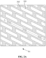
- FIG. 2A is a top view
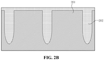
- FIG. 2B is a cross-sectional diagram along a line A-A in FIG. 2A .
- a semiconductor substrate is provided.
- the semiconductor substrate has multiple separate active areas 201 that are isolated from each other by shallow trench isolation areas 202.
- the material of the semiconductor substrate may be such as Silicon (Si), Germanium (Ge), Silicon Germanium (GeSi), or Silicon Carbide (SiC), or may be Silicon on Insulator (SOI) or Germanium on Insulator (GOI), or may be other materials, e.g., III-V compounds such as gallium arsenide.
- the material of the semiconductor substrate is Silicon.
- Certain foreign ions are doped in the semiconductor substrate according to requirements.
- the foreign ions may be N-type foreign ions or P-type foreign ions.
- the doping includes well area doping and source/drain area doping.
- a method for forming the active areas 201 includes the following steps. Multiple shallow trenches are formed by etching on the semiconductor substrate by means of lithography.
- the shallow trench isolation areas 202 are formed by filling the shallow trenches with an isolation material.
- the isolation material includes, but is not limited to, silicon oxide, silicon nitride, silicon oxynitride, or other suitable isolation materials. In the embodiment, the isolation material refers to silicon oxide.
- Portions, isolated by the shallow trench isolation areas 202, of the semiconductor substrate are the active areas 202. In the embodiment, as illustrated in FIG. 2A , the active areas 201 extend along a direction B1. The active areas 201 in adjacent rows may be staggered to a certain degree in location.
- the isolation material when the shallow trenches are filled with the isolation material, the isolation material also covers an upper surface of the semiconductor substrate. That is, upper surfaces of the active areas 210 are also covered with the isolation material. In FIG. 2A , since the active areas 201 are covered by the isolation material, the active areas 201 are drawn with dotted lines.
- the isolation material on the upper surface of the semiconductor substrate is removed, and only the isolation material located inside the shallow trenches is remained. Or in the process of filling the shallow trenches with the isolation material, only insides of the shallow trenches are filled with the isolation material, and the upper surface of the semiconductor substrate is not covered with the isolation material.
- a sacrificial layer 210 is formed on a surface of the semiconductor substrate, and the sacrificial layer 210 covers the active areas 201 and the shallow trench isolation areas 202.
- the material of the sacrificial layer 210 includes one or more of silicon dioxide, silicon nitride, silicon oxynitride, polysilicon, monocrystalline silicon, and carbon.
- the trenches 203 include a first trench 203A and a second trench 203B; the first trench 203A is located in the active area 201, and the second trench 203B is located in the shallow trench isolation area 202; and a width of the first trench 203A is greater than a width of the second trench 203B.
- the sacrificial layer 210 may be correspondingly etched to form the trench 203 during performing of the step S11.
- the trenches 203 can be formed using lithography and etching processes.
- the widths of the first trench 203 and the second trench 203B are controlled by changing an etch rate of an etching substance on the shallow trench isolation areas 202 and an etch rate of an etching substance on the active areas 201. That is, the widths of the first trench 203A and the second trench 203B are controlled by controlling an etch selection ratio of the etching substance on the shallow trench isolation areas 202 and on the active areas 201.
- the etch rate of the etching substance on the shallow trench isolation areas 202 is less than the etch rate of the etching substance on the active areas 201, so that the width of the first trench 203A is greater than the width of the second trench 203B.
- the shallow trench isolation areas 202 are silicon dioxide isolation areas
- the active areas 201 are silicon active areas.
- the method for forming the trench includes the following steps.
- a mask layer 220 and a photoresist layer 230 are formed on the sacrificial layer 210.
- the mask layer 220 may be a single layer or multiple layers.
- the mask layer 220 includes a carbon layer 221 and a silicon oxynitride (SION) layer 222 which are arranged in sequence.
- the photoresist layer 230 is patterned to form a window 231. Specifically, in this step, the photoresist layer 230 is patterned using an ashing method.
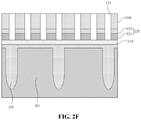
- the mask layer 220 is etched along the window 231 to expose the sacrificial layer 210.
- HBr and CF 4 may be used as etching gases to remove the SION layer 222
- O 2 , SO 2 , and Ar may be used as etching gases to remove the carbon layer 221.
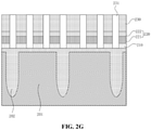
- the sacrificial layer 210 is continued to be etched to expose the active areas and the shallow trench isolation areas.
- CF 4 , CH 2 F 2 and He may be used as etching gases to remove the sacrificial layer 210 to expose the active areas and the shallow trench isolation areas.
- Cl 2 , HBr, CF 4 , and CHF 3 are used as gas sources, and the active areas 201 and the shallow trench isolation areas 202 are etched for the first time using a plasma process for a certain period of time.
- the etch rate of Cl 2 , HBr, CF 4 , and CHF 3 on silicon is greater than the etch rate of Cl 2 , HBr, CF 4 , and CHF 3 on silicon dioxide.
- the etching parameters such as an etching time, may be controlled in this step to initially form the first trench 203 with a preset width.
- the shallow trench isolation areas may also be etched, with an etching amount much less than that of silicon.
- the photoresist layer 230 and the mask layer 220 may be gradually removed by etching during an etching process. If the photoresist layer 230 and the mask layer 220 are not completely removed before the step of forming the first trench 203A as illustrated in FIG. 2H , the remaining photoresist layer 230 and mask layer 220 will be removed using processes such as ashing and etching.
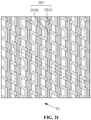
- FIG. 2I is a top view
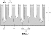
- FIG. 2J is a cross-sectional diagram along a line A-A in FIG. 2I .
- CF 4 and CHF 3 are used as gas sources
- the active areas 201 and the shallow trench isolation areas 202 are etched for the second time using the plasma process for a certain period of time.
- an etch rate of CF 4 and CHF 3 on silicon dioxide is greater than the etch rate of CF 4 and CHF 3 on silicon.
- the etching parameters such as an etching time may be controlled in this step to form the second trench 203B with a preset width.
- the active areas 201 may be continued to be etched, with an etching amount much less than that of silicon dioxide.
- a step of cleaning by-products is further included.
- O 2 is used to act on the first trench 203A and the second trench 203B for a certain period of time to clean the by-products.
- a width W1 of the first trench 203A formed using the above method is greater than a width W2 of the second trench 203B formed using the above method. It should be understood that those skilled in the art may adopt other methods to form the trenches. Since the width W1 of the first trench 203A is greater than the width W2 of the second trench 203B, widths of a first word line and second lines subsequently formed are also different.
- the width W1 of the first trench 203A ranges from 20nm to 30nm
- the width W2 of the second trench 203B ranges from 17nm to 25nm.
- a difference between the width W1 of the first trench 203A and the width W2 of the second trench 203B ranges from 4nm to 10nm. If a size of the second trench 203B is too small, a width of a second word line 270B (shown in FIG. 2L ) subsequently formed in the second trench 203B may be too small, resulting in a large word line resistance and slow switch-on of a transistor.
- a depth D1 of the first trench 203A is less than a depth D2 of the second trench 203B, and thus depths of the first word line and the second word line subsequently formed are also different.
- the word lines are formed in the trenches 203.
- the word lines include a first word line and a second word line.
- the first word line is located in the first trench, and the second word line is located in the second trench.
- the width of the first word line is greater than a width of the second word line.
- a dielectric layer 240, an adhesion layer 250, and a conductive layer 260 are formed in the trench 203 in sequence.
- the dielectric layer 240 covers at least an internal surface of the trenches 203
- the adhesion layer 250 covers at least the dielectric layer 240
- the conductive layer 260 fills at least the trenches 203.
- the dielectric layer 240 and the adhesion layer 250 are only formed in the trenches 203.
- the dielectric layer 240 and the adhesion layer 250 are also formed on the upper surface of the sacrificial layer 210 in sequence.
- the dielectric layer 240 and the adhesion layer 250 on the surface of the sacrificial layer 210 are removed.
- the conductive layer 260 also covers the upper surface of the sacrificial layer 210.
- the dielectric layer 240 may be an oxide layer, which may serve as a gate oxide layer.
- the dielectric layer 240 may be formed using an In-Situ Steam Generation (ISSG) process. It should be understood that if the dielectric layer 240 is formed by the ISSG process, due to the fact that the material of the shallow trench isolation areas 202 cannot be oxidized, the dielectric layer 240 may be only formed in the first trench 203A of the active area 201, and may not be formed in the second trench 203B of the shallow trench isolation area 202. If the dielectric layer 240 is formed using a deposition method or the like, the dielectric layer 240 may be formed in both the first trench 203A and the second trench 203B.
- ISSG In-Situ Steam Generation
- the adhesion layer 250 may be a titanium nitride layer, and the conductive layer 260 may be a metal tungsten layer.
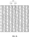
- FIG. 2L is a top view
- FIG. 2M is a cross-sectional diagram along a line A-A in FIG. 2M .
- the word lines 270 are formed by removing part of the adhesion layer 250 and the conductive layer 260. An upper surface of the word lines 270 is lower than the surface of the semiconductor substrate.
- the conductive layer 260 is etched to a preset height, and part of the adhesion layer 250 which is not covered by the conductive layer 260 is removed, so that the word lines 270 are formed.
- a first word line 270A is formed in the first trench 203A
- a second word line 270B is formed in the second trench 203B.
- the dielectric layer 240 and the adhesion layer 250 are thin, in order to avoid line overlapping in the figures, the dielectric layer 240 and the adhesion layer 250 are not illustrated in FIG. 2K . It should be understood that in this step, the dielectric layer 240 may be partially removed or thinned with performing of the etching process.
- an upper surface of the adhesion layer 250 is lower than an upper surface of the conductive layer 260 to reduce a Gate Induce Drain Leakage (GIDL) effect.
- GIDL Gate Induce Drain Leakage
- a width C1 of the first word line 270A is greater than a width C2 of the second word line 270B. Since a thickness H of the shallow trench isolation area 202 between the second word line 270B and the active area 210 adjacent thereto is large enough, when the second word line 270B is powered to work, an inversion layer, on the active area 201, induced by the second word line 270B has a small or no thickness, which is not enough to form a parasitic transistor structure, so that the leakage current will not be generated, and the storage performance of the semiconductor device is greatly improved.
- the first word line and the second word line have the same width.
- an inversion layer, on the active area adjacent thereto, induced by the second word line has a large thickness, so that a parasitic transistor structure can be formed, and the leakage current may be generated.
- a distance H1 from the bottom of the first word line 270A to the surface of the semiconductor substrate is less than a distance H2 from the bottom of the second word line 270B to the surface of the semiconductor substrate, so that a fin-shaped structure is formed to increase a channel width and improve performance of the transistor of the semiconductor device formed subsequently.
- the distance H1 from the bottom of the first word line 270A to the surface of the semiconductor substrate ranges from 140nm to 165nm
- the distance H2 from the bottom of the second word line 270B to the surface of the semiconductor substrate ranges from 175nm to 190nm.
- the method further includes the following step: referring to FIG. 2N , a protective layer 280 is filled.
- the protective layer 280 covers at least the word lines 270 to avoid the conductive layer 260 being oxidized.
- the protective layer 280 may be a SiN layer. In this embodiment, the protective layer 280 also covers the surface of the sacrificial layer 210.
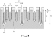
- FIG. 3A and FIG. 3B are structural schematic diagrams of a semiconductor structure according to an embodiment of the disclosure.
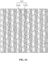
- FIG. 3A is a top view
- FIG. 3B is a cross-sectional diagram along a line A-A in FIG. 3A .
- the semiconductor structure includes a semiconductor substrate and word lines 370.
- the semiconductor substrate has multiple separate active areas 301 that are isolated from each other by shallow trench isolation areas 302.
- the word lines 370 include a first word line 370A and a word line 370B.
- the first word line 370A is located in the active area 301
- the second word line 370B is located in the shallow trench isolation area 302.
- a width C1 of the first word line 370A is greater than a width C2 of the second word line 370B.
- the width C1 of the first word line 370A ranges from 20nm to 30nm
- the width C2 of the second word line 370B ranges from 17nm to 25nm.
- a difference between the width of the first word line 370A and the width of the second word line 370B ranges from 4nm to 10nm.
- word line resistance may be large and switch-on of a transistor may be slow.
- a distance H1 from the bottom of the first word line 370A to the surface of the semiconductor substrate is less than a distance H2 from the bottom of the second word line 370B to the surface of the semiconductor substrate, so that a fin-shaped structure is formed to increase a channel width and improve performance of the transistor of the semiconductor device formed subsequently.
- the distance H1 from the bottom of the first word line 370A to the surface of the semiconductor substrate ranges from 140nm to 165nm
- the distance H2 from the bottom of the second word line 370B to the surface of the semiconductor substrate ranges from 175nm to 190nm.
- first word line 370A and the second word line 370B are flush, and a distance H3 from the upper surfaces of the first word line 370A and the second word line 370B to the surface of the semiconductor substrate ranges from 60nm to 75nm.
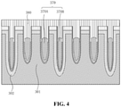
- FIG. 4 is a structural schematic diagram of a semiconductor structure according to another embodiment of the disclosure.
- a thickness H of each shallow trench isolation area 302 between the respective second word line 370B and the respective active area 301 adjacent thereto is large enough, when the second word line 370B is powered to work, an inversion layer, on the active area 301, induced by the second word line 370B has a small or no thickness, which is not enough to form a parasitic transistor structure, so that leakage current will not be generated, and storage performance of the semiconductor device is greatly improved.
Landscapes
- Engineering & Computer Science (AREA)
- Manufacturing & Machinery (AREA)
- Element Separation (AREA)
- Semiconductor Memories (AREA)
Abstract
Description
- This application claims priority to
Chinese Patent Application No. 202010419476.4, filed on May 18, 2020 - The disclosure relates to the technical field of semiconductors, in particular, to a semiconductor structure and a method for forming the semiconductor structure.
- Semiconductor devices have been widely used in integrated circuits. For example, dynamic random access memories are a type of semiconductor memories widely used in the integrated circuits. With a continuous decrease of characteristic sizes of semiconductor integrated circuit devices, semiconductor devices are also constantly developing towards a high integration density, and therefore, more severe challenges are presented to the semiconductor forming technology.
- With a continuous increase of the integration density of the semiconductor devices, the semiconductor devices may generate leakage current, which will affect storage performance thereof.
- Thus, how to effectively reduce the leakage current and improve the storage performance of the semiconductor devices is a technical problem urgent to be solved currently.
- The technical problem to be solved by the disclosure is to provide a semiconductor structure and a method for forming the semiconductor structure, which can reduce the leakage current of the semiconductor structure and improve the storage performance of a semiconductor device.
- In order to solve the above technical problem, the present disclosure provides a method for forming a semiconductor structure, the method includes: providing a semiconductor substrate, which has multiple separate active areas that are isolated from each other by shallow trench isolation areas; forming trenches by etching the active areas and the shallow trench isolation areas, herein the trenches include first trenches and second trenches, the first trenches are located in the active areas, the second trenches are located in the shallow trench isolation areas, and the first trenches have a width greater than a width of the second trenches; forming word lines in the trenches, herein the word lines include first word lines and second word lines, each first word line is located in a respective first trench, each second word line is located in a respective second trench, and the first word lines have a width greater than a width of the second word lines.
- Further, in the step of forming the trenches by etching the active areas and the shallow trench isolation areas, an etch rate of an etching substance on the shallow trench isolation areas is less than an etch rate of an etching substance on the active areas, so that the first trenches have the width greater than the width of the second trenches.
- Further, the first trenches have a depth less than a depth of the second trenches, and a distance from a bottom of the first word lines to a surface of the semiconductor substrate is less than a distance from a bottom of the second trenches to the surface of the semiconductor substrate.
- Further, before forming the trenches by etching the active areas and the shallow trench isolation areas, the method further includes: forming a sacrificial layer on the surface of the semiconductor substrate, herein the sacrificial layer covers the active areas and the shallow trench isolation areas; and forming the trenches by etching the active areas and the shallow trench isolation areas includes: forming the trenches by etching the sacrificial layer, the active areas, and the shallow trench isolation areas.
- Further, forming the word lines in the trenches further includes: forming a dielectric layer, an adhesion layer, and a conductive layer in the trenches in sequence, herein the dielectric layer covers at least an internal surface of the trenches, the adhesion layer covers at least the dielectric layer, and the conductive layer fills at least the trenches; and forming the word lines by removing part of the adhesion layer and the conductive layer, herein the word lines have an upper surface lower than a surface of the substrate.
- Further, after forming the word lines in the trenches, a protective layer is filled, the protective layer covering at least the word lines.
- In order to solve the above problem, the present disclosure further provides a semiconductor substrate formed by the above-mentioned method for forming a semiconductor structure. The semiconductor structure includes a semiconductor substrate, which has multiple separate active areas that are isolated from each other by shallow trench isolation areas; and word lines, including first word lines and second word lines. Herein the first word lines are located in the active areas, the second word lines are located in the shallow trench isolation areas, and the first word lines have a width greater than a width of the second word lines.
- Further, a difference between the width of the first word lines and the width of the second word lines ranges from 4nm to 10nm.
- Further, the width of the first word lines ranges from 20nm to 30nm, and the width of the second word lines ranges from 17nm to 25nm.
- Further, a distance from the bottom of the first word lines to the surface of the semiconductor substrate is less than a distance from the bottom of the second word lines to the surface of the semiconductor substrate.
- Further, the distance from the bottom of the first word lines to the surface of the semiconductor substrate ranges from 140nm to 165nm, and the distance from the bottom of the second word lines to the surface of the semiconductor substrate ranges from 175nm to 190nm.
- Further, the upper surface of the word lines is lower than the surface of the semiconductor substrate.
- Further, a distance from the upper surface of the word lines to the surface of the semiconductor substrate ranges from 60nm to 75nm.
- Further, each word line includes a dielectric layer, an adhesion layer, and a conductive layer which are arranged in sequence.
- Further, the adhesion layer has an upper surface lower than an upper surface of the conductive layer.
- Further, the semiconductor structure also includes a protective layer which covers at least the word lines.
- Further, a depth of the first word lines ranges from 65nm to 105nm, a depth of the second word lines ranges from 100nm to 130nm, the width of the first word lines ranges from 20nm to 30nm, and the width of the second word lines ranges from 17nm to 25nm.
- The present disclosure has the advantages that for the semiconductor structure formed by the method for forming a semiconductor structure of the present disclosure, if a thickness of each shallow trench isolation area between the respective second word line and the respective adjacent active area is large enough, when the second word lines are powered to work, an inversion layer, on the active areas, induced by the second word lines has a small or no thickness, which is not enough to form a parasitic transistor structure, so that there is no leakage current generated, and the storage performance of the semiconductor device is greatly improved.
- In order to describe the technical solutions of the embodiments in the disclosure more clearly, reference will now be made to the accompanying drawings required for the embodiments of the disclosure. It is apparent that the accompanying drawings in the following descriptions are only some embodiments of the disclosure. Other drawings may be obtained by those ordinary skilled in the art according to these accompanying drawings without involving any inventive work.
-
FIG. 1 is a schematic diagram of steps of a method for forming a semiconductor structure according to an embodiment of the disclosure. -
FIG. 2A to FIG. 2N are flowcharts of the process of a method for forming a semiconductor structure according to an embodiment of the disclosure. -
FIG. 3A andFIG. 3B are structural schematic diagrams of a semiconductor structure according to an embodiment of the disclosure. -
FIG. 4 is a structural schematic diagram of a semiconductor structure according to another embodiment of the disclosure. - In order to make the objectives, technical manners, and effects of the disclosure clearer, the disclosure will be described further below in conjunction with the accompany drawings. It should to be understood that the embodiments described here are only part of the embodiments of the disclosure, not all of the embodiments, and not intended to limit the disclosure. All other embodiments obtained by those skilled in the art on the basis of the embodiments of the disclosure without involving any inventive work shall fall within the scope of protection of the disclosure.
- With a continuous increase of an integration density of a semiconductor device, the semiconductor device may generate leakage current. Through research, the applicant found that a cause of the leakage current is that a parasitic transistor structure is formed in a semiconductor structure. The parasitic transistor structure may generate the leakage current in the semiconductor device.
- Through further research, the applicant found that in the semiconductor structure, a buried Word Line (WL) may simultaneously pass through an Active Area (AA) and a Shallow Trench Isolation (STI) area; and when working, the buried word line in the shallow trench isolation area may induce an inversion layer on the active area adjacent the shallow trench isolation area so as to form the parasitic transistor structure, thereby generating the leakage current.
- Therefore, the disclosure provides a semiconductor structure and a method for manufacturing the semiconductor structure, which can avoid the formation of the parasitic transistor structure so as to avoid generating the leakage current in the semiconductor structure.
-
FIG. 1 is a schematic diagram of steps of a method for forming a semiconductor structure according to an embodiment of the disclosure. Referring toFIG. 1 , the method for forming a semiconductor structure includes steps S10 to S12. At S10, a semiconductor substrate is provided, and the semiconductor substrate has multiple separate active areas that are isolated from each other by shallow trench isolation areas. At S11, the trenches are formed by etching the active areas and the shallow trench isolation areas, herein the trenches include first trenches and second trenches, the first trenches are located in the active areas, the second trenches are located in the shallow trench isolation areas, and the first trenches have a width greater than a width of the second trenches. At S12, the word lines are formed in the trenches, herein the word lines include first word lines and second word lines, each first word line is located in a respective first trench, each second word line is located in a respective second trench, and the first word lines have a width greater than a width of the second word lines. -
FIG. 2A to FIG. 2N are flowcharts of the process of a method for forming a semiconductor structure according to an embodiment of the disclosure. - Referring to S10, and
FIG. 2A andFIG. 2B , hereinFIG. 2A is a top view, andFIG. 2B is a cross-sectional diagram along a line A-A inFIG. 2A . A semiconductor substrate is provided. The semiconductor substrate has multiple separateactive areas 201 that are isolated from each other by shallowtrench isolation areas 202. - The material of the semiconductor substrate may be such as Silicon (Si), Germanium (Ge), Silicon Germanium (GeSi), or Silicon Carbide (SiC), or may be Silicon on Insulator (SOI) or Germanium on Insulator (GOI), or may be other materials, e.g., III-V compounds such as gallium arsenide. In this embodiment, the material of the semiconductor substrate is Silicon. Certain foreign ions are doped in the semiconductor substrate according to requirements. The foreign ions may be N-type foreign ions or P-type foreign ions. In an embodiment, the doping includes well area doping and source/drain area doping.
- A method for forming the
active areas 201 is provided in the disclosure and the method includes the following steps. Multiple shallow trenches are formed by etching on the semiconductor substrate by means of lithography. The shallowtrench isolation areas 202 are formed by filling the shallow trenches with an isolation material. The isolation material includes, but is not limited to, silicon oxide, silicon nitride, silicon oxynitride, or other suitable isolation materials. In the embodiment, the isolation material refers to silicon oxide. Portions, isolated by the shallowtrench isolation areas 202, of the semiconductor substrate are theactive areas 202. In the embodiment, as illustrated inFIG. 2A , theactive areas 201 extend along a direction B1. Theactive areas 201 in adjacent rows may be staggered to a certain degree in location. - In the embodiment, when the shallow trenches are filled with the isolation material, the isolation material also covers an upper surface of the semiconductor substrate. That is, upper surfaces of the
active areas 210 are also covered with the isolation material. InFIG. 2A , since theactive areas 201 are covered by the isolation material, theactive areas 201 are drawn with dotted lines. In other embodiments of the disclosure, after the shallow trenches are filled with the isolation material, the isolation material on the upper surface of the semiconductor substrate is removed, and only the isolation material located inside the shallow trenches is remained. Or in the process of filling the shallow trenches with the isolation material, only insides of the shallow trenches are filled with the isolation material, and the upper surface of the semiconductor substrate is not covered with the isolation material. - Optionally, after the step of S10, the following steps are included. Referring to S100 and
FIG. 2C , asacrificial layer 210 is formed on a surface of the semiconductor substrate, and thesacrificial layer 210 covers theactive areas 201 and the shallowtrench isolation areas 202. The material of thesacrificial layer 210 includes one or more of silicon dioxide, silicon nitride, silicon oxynitride, polysilicon, monocrystalline silicon, and carbon. - Referring to S11, and
FIG. 2D to FIG. 2I , theactive areas 201 and the shallowtrench isolation areas 202 are etched to form the trenches. Thetrenches 203 include afirst trench 203A and asecond trench 203B; thefirst trench 203A is located in theactive area 201, and thesecond trench 203B is located in the shallowtrench isolation area 202; and a width of thefirst trench 203A is greater than a width of thesecond trench 203B. - In the embodiment, since there is also a
sacrificial layer 210 on the surface of the semiconductor substrate, thesacrificial layer 210 may be correspondingly etched to form thetrench 203 during performing of the step S11. - In this step, the
trenches 203 can be formed using lithography and etching processes. During etching, the widths of thefirst trench 203 and thesecond trench 203B are controlled by changing an etch rate of an etching substance on the shallowtrench isolation areas 202 and an etch rate of an etching substance on theactive areas 201. That is, the widths of thefirst trench 203A and thesecond trench 203B are controlled by controlling an etch selection ratio of the etching substance on the shallowtrench isolation areas 202 and on theactive areas 201. Specifically, the etch rate of the etching substance on the shallowtrench isolation areas 202 is less than the etch rate of the etching substance on theactive areas 201, so that the width of thefirst trench 203A is greater than the width of thesecond trench 203B. - An embodiment of a method for forming the trenches is set forth as below. In the embodiment, the shallow
trench isolation areas 202 are silicon dioxide isolation areas, and theactive areas 201 are silicon active areas. The method for forming the trench includes the following steps. - Referring to
FIG. 2D , amask layer 220 and aphotoresist layer 230 are formed on thesacrificial layer 210. Themask layer 220 may be a single layer or multiple layers. In the embodiment, themask layer 220 includes acarbon layer 221 and a silicon oxynitride (SION)layer 222 which are arranged in sequence. - Referring to
FIG. 2E , thephotoresist layer 230 is patterned to form awindow 231. Specifically, in this step, thephotoresist layer 230 is patterned using an ashing method. - Referring to
FIG. 2F , themask layer 220 is etched along thewindow 231 to expose thesacrificial layer 210. In this step, HBr and CF4 may be used as etching gases to remove theSION layer 222, and O2, SO2, and Ar may be used as etching gases to remove thecarbon layer 221. - Referring to
FIG. 2G , thesacrificial layer 210 is continued to be etched to expose the active areas and the shallow trench isolation areas. In this step, CF4, CH2F2 and He may be used as etching gases to remove thesacrificial layer 210 to expose the active areas and the shallow trench isolation areas. - Referring to
FIG. 2H , Cl2, HBr, CF4, and CHF3 are used as gas sources, and theactive areas 201 and the shallowtrench isolation areas 202 are etched for the first time using a plasma process for a certain period of time. In this step, the etch rate of Cl2, HBr, CF4, and CHF3 on silicon is greater than the etch rate of Cl2, HBr, CF4, and CHF3 on silicon dioxide. Accordingly, the etching parameters, such as an etching time, may be controlled in this step to initially form thefirst trench 203 with a preset width. It should be understood that in this step, the shallow trench isolation areas may also be etched, with an etching amount much less than that of silicon. - The
photoresist layer 230 and themask layer 220 may be gradually removed by etching during an etching process. If thephotoresist layer 230 and themask layer 220 are not completely removed before the step of forming thefirst trench 203A as illustrated inFIG. 2H , the remainingphotoresist layer 230 andmask layer 220 will be removed using processes such as ashing and etching. - Referring to
FIG. 2I andFIG. 2J ,FIG. 2I is a top view, andFIG. 2J is a cross-sectional diagram along a line A-A inFIG. 2I . CF4 and CHF3 are used as gas sources, theactive areas 201 and the shallowtrench isolation areas 202 are etched for the second time using the plasma process for a certain period of time. In this step, an etch rate of CF4 and CHF3 on silicon dioxide is greater than the etch rate of CF4 and CHF3 on silicon. Accordingly, the etching parameters such as an etching time may be controlled in this step to form thesecond trench 203B with a preset width. It should be understood that, in this step, theactive areas 201 may be continued to be etched, with an etching amount much less than that of silicon dioxide. - Further, after etching, a step of cleaning by-products is further included. For example, O2 is used to act on the
first trench 203A and thesecond trench 203B for a certain period of time to clean the by-products. - A width W1 of the
first trench 203A formed using the above method is greater than a width W2 of thesecond trench 203B formed using the above method. It should be understood that those skilled in the art may adopt other methods to form the trenches. Since the width W1 of thefirst trench 203A is greater than the width W2 of thesecond trench 203B, widths of a first word line and second lines subsequently formed are also different. - Further, the width W1 of the
first trench 203A ranges from 20nm to 30nm, and the width W2 of thesecond trench 203B ranges from 17nm to 25nm. A difference between the width W1 of thefirst trench 203A and the width W2 of thesecond trench 203B ranges from 4nm to 10nm. If a size of thesecond trench 203B is too small, a width of asecond word line 270B (shown inFIG. 2L ) subsequently formed in thesecond trench 203B may be too small, resulting in a large word line resistance and slow switch-on of a transistor. - Further, in the embodiment, a depth D1 of the
first trench 203A is less than a depth D2 of thesecond trench 203B, and thus depths of the first word line and the second word line subsequently formed are also different. - Referring to S12, the word lines are formed in the
trenches 203. The word lines include a first word line and a second word line. The first word line is located in the first trench, and the second word line is located in the second trench. The width of the first word line is greater than a width of the second word line. - An embodiment of a method for forming the word lines is set forth as below.
- Referring to
FIG. 2K , adielectric layer 240, anadhesion layer 250, and aconductive layer 260 are formed in thetrench 203 in sequence. Thedielectric layer 240 covers at least an internal surface of thetrenches 203, theadhesion layer 250 covers at least thedielectric layer 240, and theconductive layer 260 fills at least thetrenches 203. In this embodiment, thedielectric layer 240 and theadhesion layer 250 are only formed in thetrenches 203. In other embodiments of the disclosure, under influences of preparation processes, thedielectric layer 240 and theadhesion layer 250 are also formed on the upper surface of thesacrificial layer 210 in sequence. Before forming theconductive layer 260, thedielectric layer 240 and theadhesion layer 250 on the surface of thesacrificial layer 210 are removed. In the embodiment, theconductive layer 260 also covers the upper surface of thesacrificial layer 210. - The
dielectric layer 240 may be an oxide layer, which may serve as a gate oxide layer. Thedielectric layer 240 may be formed using an In-Situ Steam Generation (ISSG) process. It should be understood that if thedielectric layer 240 is formed by the ISSG process, due to the fact that the material of the shallowtrench isolation areas 202 cannot be oxidized, thedielectric layer 240 may be only formed in thefirst trench 203A of theactive area 201, and may not be formed in thesecond trench 203B of the shallowtrench isolation area 202. If thedielectric layer 240 is formed using a deposition method or the like, thedielectric layer 240 may be formed in both thefirst trench 203A and thesecond trench 203B. - The
adhesion layer 250 may be a titanium nitride layer, and theconductive layer 260 may be a metal tungsten layer. - Referring to
FIG. 2L andFIG. 2M ,FIG. 2L is a top view, andFIG. 2M is a cross-sectional diagram along a line A-A inFIG. 2M . The word lines 270 are formed by removing part of theadhesion layer 250 and theconductive layer 260. An upper surface of the word lines 270 is lower than the surface of the semiconductor substrate. In the step, theconductive layer 260 is etched to a preset height, and part of theadhesion layer 250 which is not covered by theconductive layer 260 is removed, so that the word lines 270 are formed. Afirst word line 270A is formed in thefirst trench 203A, and asecond word line 270B is formed in thesecond trench 203B. Because thedielectric layer 240 and theadhesion layer 250 are thin, in order to avoid line overlapping in the figures, thedielectric layer 240 and theadhesion layer 250 are not illustrated inFIG. 2K . It should be understood that in this step, thedielectric layer 240 may be partially removed or thinned with performing of the etching process. - Further, in a formed word lines structure, an upper surface of the
adhesion layer 250 is lower than an upper surface of theconductive layer 260 to reduce a Gate Induce Drain Leakage (GIDL) effect. - Referring to
FIG. 2M , since the width W1 of thefirst trench 203A is greater than the width W2 of thesecond trench 203B, a width C1 of thefirst word line 270A is greater than a width C2 of thesecond word line 270B. Since a thickness H of the shallowtrench isolation area 202 between thesecond word line 270B and theactive area 210 adjacent thereto is large enough, when thesecond word line 270B is powered to work, an inversion layer, on theactive area 201, induced by thesecond word line 270B has a small or no thickness, which is not enough to form a parasitic transistor structure, so that the leakage current will not be generated, and the storage performance of the semiconductor device is greatly improved. In certain technical solutions, the first word line and the second word line have the same width. When the second word line is powered to work, an inversion layer, on the active area adjacent thereto, induced by the second word line has a large thickness, so that a parasitic transistor structure can be formed, and the leakage current may be generated. - Further, since a depth D1 of the
first trench 203A is less than a depth D2 of thesecond trench 203B, a distance H1 from the bottom of thefirst word line 270A to the surface of the semiconductor substrate is less than a distance H2 from the bottom of thesecond word line 270B to the surface of the semiconductor substrate, so that a fin-shaped structure is formed to increase a channel width and improve performance of the transistor of the semiconductor device formed subsequently. Further, the distance H1 from the bottom of thefirst word line 270A to the surface of the semiconductor substrate ranges from 140nm to 165nm, and the distance H2 from the bottom of thesecond word line 270B to the surface of the semiconductor substrate ranges from 175nm to 190nm. - Further, the upper surfaces of the
first word line 270A and thesecond word line 270B are flush, and a distance H3 from the upper surfaces of thefirst word line 270A and thesecond word line 270B to the surface of the semiconductor substrate ranges from 60nm to 75nm. Further, after the step of S12, the method further includes the following step: referring toFIG. 2N , aprotective layer 280 is filled. Theprotective layer 280 covers at least the word lines 270 to avoid theconductive layer 260 being oxidized. Theprotective layer 280 may be a SiN layer. In this embodiment, theprotective layer 280 also covers the surface of thesacrificial layer 210. - The disclosure further provides a semiconductor structure formed by using the above fabrication methods.
FIG. 3A andFIG. 3B are structural schematic diagrams of a semiconductor structure according to an embodiment of the disclosure.FIG. 3A is a top view, andFIG. 3B is a cross-sectional diagram along a line A-A inFIG. 3A . Referring toFIG. 3A andFIG. 3B , the semiconductor structure includes a semiconductor substrate and word lines 370. - The semiconductor substrate has multiple separate
active areas 301 that are isolated from each other by shallowtrench isolation areas 302. - The word lines 370 include a
first word line 370A and aword line 370B. Thefirst word line 370A is located in theactive area 301, and thesecond word line 370B is located in the shallowtrench isolation area 302. A width C1 of thefirst word line 370A is greater than a width C2 of thesecond word line 370B. Further, the width C1 of thefirst word line 370A ranges from 20nm to 30nm, and the width C2 of thesecond word line 370B ranges from 17nm to 25nm. A difference between the width of thefirst word line 370A and the width of thesecond word line 370B ranges from 4nm to 10nm. Herein, if the width of thesecond word line 370B is too small, word line resistance may be large and switch-on of a transistor may be slow. - Further, a distance H1 from the bottom of the
first word line 370A to the surface of the semiconductor substrate is less than a distance H2 from the bottom of thesecond word line 370B to the surface of the semiconductor substrate, so that a fin-shaped structure is formed to increase a channel width and improve performance of the transistor of the semiconductor device formed subsequently. Further, the distance H1 from the bottom of thefirst word line 370A to the surface of the semiconductor substrate ranges from 140nm to 165nm, and the distance H2 from the bottom of thesecond word line 370B to the surface of the semiconductor substrate ranges from 175nm to 190nm. - Further, upper surfaces of the
first word line 370A and thesecond word line 370B are flush, and a distance H3 from the upper surfaces of thefirst word line 370A and thesecond word line 370B to the surface of the semiconductor substrate ranges from 60nm to 75nm. -
FIG. 4 is a structural schematic diagram of a semiconductor structure according to another embodiment of the disclosure. - In the disclosure, a thickness H of each shallow
trench isolation area 302 between the respectivesecond word line 370B and the respectiveactive area 301 adjacent thereto is large enough, when thesecond word line 370B is powered to work, an inversion layer, on theactive area 301, induced by thesecond word line 370B has a small or no thickness, which is not enough to form a parasitic transistor structure, so that leakage current will not be generated, and storage performance of the semiconductor device is greatly improved. - The above are only preferred implementations of the disclosure. It should be understood that those ordinary skilled in the art may also make several improvements and modifications without departing from the principle of the disclosure. These improvements and modifications shall fall within the scope of protection of the disclosure.
Claims (18)
- A method for forming a semiconductor structure, comprising:providing a semiconductor substrate, the semiconductor substrate having a plurality of separate active areas that are isolated from each other by shallow trench isolation areas;forming trenches by etching the active areas and the shallow trench isolation areas, wherein the trenches comprise first trenches and second trenches, the first trenches are located in the active areas, the second trenches are located in the shallow trench isolation areas, and the first trenches have a width greater than a width of the second trenches; andforming word lines in the trenches, wherein the word lines comprise first word lines and second word lines, each first word line is located in a respective first trench, each second word line is located in a respective second trench, and the first word lines have a width greater than a width of the second word lines.
- The method for forming a semiconductor structure of claim 1, wherein in the step of forming the trenches by etching the active areas and the shallow trench isolation areas, an etch rate of an etching substance on the shallow trench isolation areas is less than an etch rate of an etching substance on the active areas, so that the first trenches have the width greater than the width of the second trenches.
- The method for forming a semiconductor structure of claim 2, wherein the shallow trench isolation areas are silicon dioxide isolation areas, the active areas are silicon areas, and forming the trenches by etching the active areas and the shallow trench isolation areas comprises:forming a mask layer and a photoresist layer on the semiconductor substrate;forming a window by patterning the photoresist layer;exposing the silicon active areas and the silicon dioxide isolation area by etching the mask layer along the window;using Cl2, HBr, CF4, and CHF3 as gas sources, and etching, for a first time, the active areas and the silicon dioxide isolation area using a plasma process for a period of time; andusing CF4 and CHF3 as gas sources, and etching, for a second time, the active areas and the shallow trench isolation areas using the plasma process for a period of time to form the first trenches and the second trenches.
- The method for forming a semiconductor structure of claim 1, wherein the first trenches have a depth less than a depth of the second trenches, and a distance from a bottom of the first word lines to a surface of the semiconductor substrate is less than a distance from a bottom of the second trenches to the surface of the semiconductor substrate.
- The method for forming a semiconductor structure of claim 1, wherein before forming the trenches by etching the active areas and the shallow trench isolation areas, the method further comprises: forming a sacrificial layer on the surface of the semiconductor substrate, wherein the sacrificial layer covers the active areas and the shallow trench isolation areas; and forming the trenches by etching the active areas and the shallow trench isolation areas comprises: forming the trenches by etching the sacrificial layer, the active areas, and the shallow trench isolation areas.
- The method for forming a semiconductor structure of claim 1, wherein forming the word lines in the trenches further comprises:forming a dielectric layer, an adhesion layer, and a conductive layer in the trenches in sequence, wherein the dielectric layer covers at least an internal surface of the trenches, the adhesion layer covers at least the dielectric layer, and the conductive layer fills at least the trenches; andforming the word lines by removing part of the adhesion layer and the conductive layer, wherein the word lines have an upper surface lower than the surface of the substrate.
- The method for forming a semiconductor structure of claim 6, wherein after forming the word lines in the trenches, a protective layer is filled, the protective layer covering at least the word lines.
- A semiconductor structure, formed by the method for forming the semiconductor structure of claim 1, wherein the semiconductor structure comprises:a semiconductor substrate, having a plurality of separate active areas that are isolated from each other by shallow trench isolation areas; andword lines, comprising first word lines and second word lines, wherein the first word lines are located in the active areas, the second word lines are located in the shallow trench isolation areas, and the first word lines have a width greater than a width of the second word lines.
- The semiconductor structure of claim 8, wherein a difference between the width of the first word lines and the width of the second word lines ranges from 4nm to 10nm.
- The semiconductor structure of claim 8, wherein the width of the first word lines ranges from 20nm to 30nm, and the width of the second word lines ranges from 17nm to 25nm.
- The semiconductor structure of claim 8, wherein a distance from a bottom of the first word lines to a surface of the semiconductor substrate is less than a distance from a bottom of the second word lines to the surface of the semiconductor substrate.
- The semiconductor structure of claim 11, wherein the distance from the bottom of the first word lines to the surface of the semiconductor substrate ranges from 140nm to 165nm, and the distance from the bottom of the second word lines to the surface of the semiconductor substrate ranges from 175nm to 190nm.
- The semiconductor structure of claim 11, wherein an upper surface of the word lines is lower than the surface of the semiconductor substrate.
- The semiconductor structure of claim 13, wherein a distance from the upper surface of the word lines to the surface of the semiconductor substrate ranges from 60nm to 75nm.
- The semiconductor structure of claim 8, wherein each word line comprises a dielectric layer, an adhesion layer, and a conductive layer which are arranged in sequence.
- The semiconductor structure of claim 15, wherein the adhesion layer has an upper surface lower than an upper surface of the conductive layer.
- The semiconductor structure of claim 8, wherein the semiconductor structure further comprises a protective layer which covers at least the word lines.
- The semiconductor structure of claim 8, wherein a depth of the first word lines ranges from 65nm to 105nm, a depth of the second word lines ranges from 100nm to 130nm, the width of the first word lines ranges from 20nm to 30nm, and the width of the second word lines ranges from 17nm to 25nm.
Applications Claiming Priority (2)
| Application Number | Priority Date | Filing Date | Title |
|---|---|---|---|
| CN202010419476.4A CN113690185B (en) | 2020-05-18 | 2020-05-18 | Semiconductor structures and methods of forming them |
| PCT/CN2021/090098 WO2021233087A1 (en) | 2020-05-18 | 2021-04-27 | Semiconductor structure and method for forming same |
Publications (3)
| Publication Number | Publication Date |
|---|---|
| EP3955296A1 true EP3955296A1 (en) | 2022-02-16 |
| EP3955296A4 EP3955296A4 (en) | 2022-09-07 |
| EP3955296B1 EP3955296B1 (en) | 2024-10-09 |
Family
ID=78512837
Family Applications (1)
| Application Number | Title | Priority Date | Filing Date |
|---|---|---|---|
| EP21798541.5A Active EP3955296B1 (en) | 2020-05-18 | 2021-04-27 | Semiconductor structure and method for forming same |
Country Status (2)
| Country | Link |
|---|---|
| US (1) | US11871555B2 (en) |
| EP (1) | EP3955296B1 (en) |
Families Citing this family (5)
| Publication number | Priority date | Publication date | Assignee | Title |
|---|---|---|---|---|
| KR102360865B1 (en) * | 2020-08-18 | 2022-02-09 | 경상국립대학교산학협력단 | Semiconductor device and method for thereof |
| US12225713B2 (en) * | 2021-01-05 | 2025-02-11 | Changxin Memory Technologies, Inc. | Semiconductor device, manufacturing method of semiconductor device, and storage device |
| US11805640B2 (en) | 2022-01-06 | 2023-10-31 | Nanya Technology Corporation | Manufacturing method of a semiconductor device using a protect layer along a top sidewall of a trench to widen the bottom of the trench |
| CN117529084A (en) | 2022-07-28 | 2024-02-06 | 长鑫存储技术有限公司 | Manufacturing method of semiconductor structure and semiconductor structure |
| US20250157923A1 (en) * | 2023-11-14 | 2025-05-15 | Nanya Technology Corporation | Cutting structure, semiconductor device comprising the same, and method for fabricating the same |
Family Cites Families (16)
| Publication number | Priority date | Publication date | Assignee | Title |
|---|---|---|---|---|
| US6844591B1 (en) | 2003-09-17 | 2005-01-18 | Micron Technology, Inc. | Method of forming DRAM access transistors |
| KR101094376B1 (en) * | 2009-07-31 | 2011-12-15 | 주식회사 하이닉스반도체 | Method of forming a buried word line in a semiconductor device |
| KR101119774B1 (en) | 2009-08-11 | 2012-03-26 | 주식회사 하이닉스반도체 | Semiconductor device and method of fabricating the same |
| KR101096875B1 (en) | 2009-12-09 | 2011-12-22 | 주식회사 하이닉스반도체 | Method for manufacturing semiconductor having buried gate |
| US20150294975A1 (en) * | 2012-11-14 | 2015-10-15 | Ps5 Luxco S.A.R.L. | Semiconductor device and method of manufacturing the same |
| US9006077B2 (en) * | 2013-08-21 | 2015-04-14 | GlobalFoundries, Inc. | Gate length independent silicon-on-nothing (SON) scheme for bulk FinFETs |
| US9589964B1 (en) | 2015-06-24 | 2017-03-07 | Samsung Electronics Co., Ltd. | Methods of fabricating semiconductor devices |
| US9859284B2 (en) | 2016-01-21 | 2018-01-02 | Micron Technology, Inc. | Semiconductor memory device having enlarged cell contact area and method of fabricating the same |
| CN108461449B (en) * | 2017-02-20 | 2019-09-17 | 联华电子股份有限公司 | Semiconductor element and manufacturing method thereof |
| CN108962892B (en) | 2017-05-26 | 2021-02-26 | 联华电子股份有限公司 | Semiconductor element and manufacturing method thereof |
| US10867998B1 (en) * | 2017-11-29 | 2020-12-15 | Taiwan Semiconductor Manufacturing Co., Ltd. | Semiconductor structure cutting process and structures formed thereby |
| CN108899309A (en) * | 2018-06-27 | 2018-11-27 | 长鑫存储技术有限公司 | Embedded type word line structure and preparation method thereof |
| KR102596497B1 (en) * | 2018-11-16 | 2023-10-30 | 삼성전자주식회사 | Semiconductor device and method for fabricating the same |
| KR102697920B1 (en) * | 2018-11-26 | 2024-08-22 | 삼성전자주식회사 | Semiconductor device and method of fabricating the same |
| CN112447605B (en) | 2019-08-30 | 2025-01-21 | 长鑫存储技术有限公司 | DRAM memory and method of forming the same |
| CN210296376U (en) * | 2019-10-09 | 2020-04-10 | 长鑫存储技术有限公司 | Semiconductor structure and semiconductor memory |
-
2021
- 2021-04-27 EP EP21798541.5A patent/EP3955296B1/en active Active
- 2021-07-27 US US17/386,485 patent/US11871555B2/en active Active
Also Published As
| Publication number | Publication date |
|---|---|
| EP3955296B1 (en) | 2024-10-09 |
| US20210358920A1 (en) | 2021-11-18 |
| US11871555B2 (en) | 2024-01-09 |
| EP3955296A4 (en) | 2022-09-07 |
Similar Documents
| Publication | Publication Date | Title |
|---|---|---|
| EP3955296B1 (en) | Semiconductor structure and method for forming same | |
| US12471311B2 (en) | Semiconductor Fin-like field-effect transistor (FinFET) device including source/drain structure with boron doped capping layer | |
| CN110943042B (en) | Semiconductor device and integrated circuit manufacturing method | |
| US10991795B2 (en) | Semiconductor device and manufacturing method thereof | |
| CN110828541B (en) | Semiconductor structures and methods of forming them | |
| US11935957B2 (en) | Geometry for threshold voltage tuning on semiconductor device | |
| US11245036B1 (en) | Latch-up prevention | |
| US10177143B2 (en) | FinFET device and method for fabricating the same | |
| US10453741B2 (en) | Method for forming semiconductor device contact | |
| US20130153997A1 (en) | Hybrid cmos nanowire mesh device and bulk cmos device | |
| US10680109B2 (en) | CMOS semiconductor device having fins and method of fabricating the same | |
| US10109532B2 (en) | Methods of manufacturing finFET semiconductor devices | |
| US10170471B2 (en) | Bulk fin formation with vertical fin sidewall profile | |
| CN111508897A (en) | Semiconductor device and method of forming the same | |
| EP3886145A1 (en) | Method for processing a nanosheet device | |
| CN113690185B (en) | Semiconductor structures and methods of forming them | |
| CN111106010A (en) | Transistor having stacked semiconductor layers as a channel | |
| US10832975B2 (en) | Reduced static random access memory (SRAM) device foot print through controlled bottom source/drain placement | |
| CN220731538U (en) | Semiconductor devices | |
| CN119421447B (en) | Semiconductor structure and its formation method | |
| US20250374653A1 (en) | Isolation structure for nanostructure device and methods of forming the same | |
| CN120050965A (en) | Manufacturing method of complementary field effect transistor |
Legal Events
| Date | Code | Title | Description |
|---|---|---|---|
| STAA | Information on the status of an ep patent application or granted ep patent |
Free format text: STATUS: UNKNOWN |
|
| STAA | Information on the status of an ep patent application or granted ep patent |
Free format text: STATUS: THE INTERNATIONAL PUBLICATION HAS BEEN MADE |
|
| PUAI | Public reference made under article 153(3) epc to a published international application that has entered the european phase |
Free format text: ORIGINAL CODE: 0009012 |
|
| STAA | Information on the status of an ep patent application or granted ep patent |
Free format text: STATUS: REQUEST FOR EXAMINATION WAS MADE |
|
| 17P | Request for examination filed |
Effective date: 20211110 |
|
| AK | Designated contracting states |
Kind code of ref document: A1 Designated state(s): AL AT BE BG CH CY CZ DE DK EE ES FI FR GB GR HR HU IE IS IT LI LT LU LV MC MK MT NL NO PL PT RO RS SE SI SK SM TR |
|
| A4 | Supplementary search report drawn up and despatched |
Effective date: 20220808 |
|
| RIC1 | Information provided on ipc code assigned before grant |
Ipc: H01L 27/108 20060101AFI20220802BHEP |
|
| STAA | Information on the status of an ep patent application or granted ep patent |
Free format text: STATUS: EXAMINATION IS IN PROGRESS |
|
| 17Q | First examination report despatched |
Effective date: 20230512 |
|
| DAV | Request for validation of the european patent (deleted) | ||
| DAX | Request for extension of the european patent (deleted) | ||
| REG | Reference to a national code |
Ref country code: DE Ref legal event code: R079 Ref document number: 602021020066 Country of ref document: DE Free format text: PREVIOUS MAIN CLASS: H01L0027108000 Ipc: H10B0012000000 |
|
| GRAP | Despatch of communication of intention to grant a patent |
Free format text: ORIGINAL CODE: EPIDOSNIGR1 |
|
| STAA | Information on the status of an ep patent application or granted ep patent |
Free format text: STATUS: GRANT OF PATENT IS INTENDED |
|
| RIC1 | Information provided on ipc code assigned before grant |
Ipc: H10B 12/00 20230101AFI20240701BHEP |
|
| INTG | Intention to grant announced |
Effective date: 20240711 |
|
| GRAS | Grant fee paid |
Free format text: ORIGINAL CODE: EPIDOSNIGR3 |
|
| GRAA | (expected) grant |
Free format text: ORIGINAL CODE: 0009210 |
|
| STAA | Information on the status of an ep patent application or granted ep patent |
Free format text: STATUS: THE PATENT HAS BEEN GRANTED |
|
| P01 | Opt-out of the competence of the unified patent court (upc) registered |
Free format text: CASE NUMBER: APP_45064/2024 Effective date: 20240803 |
|
| AK | Designated contracting states |
Kind code of ref document: B1 Designated state(s): AL AT BE BG CH CY CZ DE DK EE ES FI FR GB GR HR HU IE IS IT LI LT LU LV MC MK MT NL NO PL PT RO RS SE SI SK SM TR |
|
| REG | Reference to a national code |
Ref country code: CH Ref legal event code: EP |
|
| REG | Reference to a national code |
Ref country code: DE Ref legal event code: R096 Ref document number: 602021020066 Country of ref document: DE |
|
| REG | Reference to a national code |
Ref country code: IE Ref legal event code: FG4D |
|
| REG | Reference to a national code |
Ref country code: LT Ref legal event code: MG9D |
|
| REG | Reference to a national code |
Ref country code: NL Ref legal event code: MP Effective date: 20241009 |
|
| REG | Reference to a national code |
Ref country code: AT Ref legal event code: MK05 Ref document number: 1732082 Country of ref document: AT Kind code of ref document: T Effective date: 20241009 |
|
| PG25 | Lapsed in a contracting state [announced via postgrant information from national office to epo] |
Ref country code: NL Free format text: LAPSE BECAUSE OF FAILURE TO SUBMIT A TRANSLATION OF THE DESCRIPTION OR TO PAY THE FEE WITHIN THE PRESCRIBED TIME-LIMIT Effective date: 20241009 |
|
| PG25 | Lapsed in a contracting state [announced via postgrant information from national office to epo] |
Ref country code: NL Free format text: LAPSE BECAUSE OF FAILURE TO SUBMIT A TRANSLATION OF THE DESCRIPTION OR TO PAY THE FEE WITHIN THE PRESCRIBED TIME-LIMIT Effective date: 20241009 |
|
| PG25 | Lapsed in a contracting state [announced via postgrant information from national office to epo] |
Ref country code: PT Free format text: LAPSE BECAUSE OF FAILURE TO SUBMIT A TRANSLATION OF THE DESCRIPTION OR TO PAY THE FEE WITHIN THE PRESCRIBED TIME-LIMIT Effective date: 20250210 Ref country code: HR Free format text: LAPSE BECAUSE OF FAILURE TO SUBMIT A TRANSLATION OF THE DESCRIPTION OR TO PAY THE FEE WITHIN THE PRESCRIBED TIME-LIMIT Effective date: 20241009 Ref country code: IS Free format text: LAPSE BECAUSE OF FAILURE TO SUBMIT A TRANSLATION OF THE DESCRIPTION OR TO PAY THE FEE WITHIN THE PRESCRIBED TIME-LIMIT Effective date: 20250209 |
|
| PG25 | Lapsed in a contracting state [announced via postgrant information from national office to epo] |
Ref country code: FI Free format text: LAPSE BECAUSE OF FAILURE TO SUBMIT A TRANSLATION OF THE DESCRIPTION OR TO PAY THE FEE WITHIN THE PRESCRIBED TIME-LIMIT Effective date: 20241009 |
|
| PG25 | Lapsed in a contracting state [announced via postgrant information from national office to epo] |
Ref country code: BG Free format text: LAPSE BECAUSE OF FAILURE TO SUBMIT A TRANSLATION OF THE DESCRIPTION OR TO PAY THE FEE WITHIN THE PRESCRIBED TIME-LIMIT Effective date: 20241009 |
|
| PG25 | Lapsed in a contracting state [announced via postgrant information from national office to epo] |
Ref country code: ES Free format text: LAPSE BECAUSE OF FAILURE TO SUBMIT A TRANSLATION OF THE DESCRIPTION OR TO PAY THE FEE WITHIN THE PRESCRIBED TIME-LIMIT Effective date: 20241009 |
|
| PG25 | Lapsed in a contracting state [announced via postgrant information from national office to epo] |
Ref country code: NO Free format text: LAPSE BECAUSE OF FAILURE TO SUBMIT A TRANSLATION OF THE DESCRIPTION OR TO PAY THE FEE WITHIN THE PRESCRIBED TIME-LIMIT Effective date: 20250109 |
|
| PG25 | Lapsed in a contracting state [announced via postgrant information from national office to epo] |
Ref country code: LV Free format text: LAPSE BECAUSE OF FAILURE TO SUBMIT A TRANSLATION OF THE DESCRIPTION OR TO PAY THE FEE WITHIN THE PRESCRIBED TIME-LIMIT Effective date: 20241009 Ref country code: GR Free format text: LAPSE BECAUSE OF FAILURE TO SUBMIT A TRANSLATION OF THE DESCRIPTION OR TO PAY THE FEE WITHIN THE PRESCRIBED TIME-LIMIT Effective date: 20250110 Ref country code: AT Free format text: LAPSE BECAUSE OF FAILURE TO SUBMIT A TRANSLATION OF THE DESCRIPTION OR TO PAY THE FEE WITHIN THE PRESCRIBED TIME-LIMIT Effective date: 20241009 |
|
| PG25 | Lapsed in a contracting state [announced via postgrant information from national office to epo] |
Ref country code: PL Free format text: LAPSE BECAUSE OF FAILURE TO SUBMIT A TRANSLATION OF THE DESCRIPTION OR TO PAY THE FEE WITHIN THE PRESCRIBED TIME-LIMIT Effective date: 20241009 |
|
| PG25 | Lapsed in a contracting state [announced via postgrant information from national office to epo] |
Ref country code: RS Free format text: LAPSE BECAUSE OF FAILURE TO SUBMIT A TRANSLATION OF THE DESCRIPTION OR TO PAY THE FEE WITHIN THE PRESCRIBED TIME-LIMIT Effective date: 20250109 |
|
| PG25 | Lapsed in a contracting state [announced via postgrant information from national office to epo] |
Ref country code: SM Free format text: LAPSE BECAUSE OF FAILURE TO SUBMIT A TRANSLATION OF THE DESCRIPTION OR TO PAY THE FEE WITHIN THE PRESCRIBED TIME-LIMIT Effective date: 20241009 |
|
| PGFP | Annual fee paid to national office [announced via postgrant information from national office to epo] |
Ref country code: DE Payment date: 20250422 Year of fee payment: 5 |
|
| PG25 | Lapsed in a contracting state [announced via postgrant information from national office to epo] |
Ref country code: DK Free format text: LAPSE BECAUSE OF FAILURE TO SUBMIT A TRANSLATION OF THE DESCRIPTION OR TO PAY THE FEE WITHIN THE PRESCRIBED TIME-LIMIT Effective date: 20241009 |
|
| REG | Reference to a national code |
Ref country code: DE Ref legal event code: R097 Ref document number: 602021020066 Country of ref document: DE |
|
| PG25 | Lapsed in a contracting state [announced via postgrant information from national office to epo] |
Ref country code: EE Free format text: LAPSE BECAUSE OF FAILURE TO SUBMIT A TRANSLATION OF THE DESCRIPTION OR TO PAY THE FEE WITHIN THE PRESCRIBED TIME-LIMIT Effective date: 20241009 |
|
| PG25 | Lapsed in a contracting state [announced via postgrant information from national office to epo] |
Ref country code: RO Free format text: LAPSE BECAUSE OF FAILURE TO SUBMIT A TRANSLATION OF THE DESCRIPTION OR TO PAY THE FEE WITHIN THE PRESCRIBED TIME-LIMIT Effective date: 20241009 |
|
| PG25 | Lapsed in a contracting state [announced via postgrant information from national office to epo] |
Ref country code: SK Free format text: LAPSE BECAUSE OF FAILURE TO SUBMIT A TRANSLATION OF THE DESCRIPTION OR TO PAY THE FEE WITHIN THE PRESCRIBED TIME-LIMIT Effective date: 20241009 |
|
| PG25 | Lapsed in a contracting state [announced via postgrant information from national office to epo] |
Ref country code: CZ Free format text: LAPSE BECAUSE OF FAILURE TO SUBMIT A TRANSLATION OF THE DESCRIPTION OR TO PAY THE FEE WITHIN THE PRESCRIBED TIME-LIMIT Effective date: 20241009 |
|
| PG25 | Lapsed in a contracting state [announced via postgrant information from national office to epo] |
Ref country code: IT Free format text: LAPSE BECAUSE OF FAILURE TO SUBMIT A TRANSLATION OF THE DESCRIPTION OR TO PAY THE FEE WITHIN THE PRESCRIBED TIME-LIMIT Effective date: 20241009 |
|
| PLBE | No opposition filed within time limit |
Free format text: ORIGINAL CODE: 0009261 |
|
| STAA | Information on the status of an ep patent application or granted ep patent |
Free format text: STATUS: NO OPPOSITION FILED WITHIN TIME LIMIT |
|
| PG25 | Lapsed in a contracting state [announced via postgrant information from national office to epo] |
Ref country code: SE Free format text: LAPSE BECAUSE OF FAILURE TO SUBMIT A TRANSLATION OF THE DESCRIPTION OR TO PAY THE FEE WITHIN THE PRESCRIBED TIME-LIMIT Effective date: 20241009 |
|
| 26N | No opposition filed |
Effective date: 20250710 |
|
| REG | Reference to a national code |
Ref country code: CH Ref legal event code: H13 Free format text: ST27 STATUS EVENT CODE: U-0-0-H10-H13 (AS PROVIDED BY THE NATIONAL OFFICE) Effective date: 20251125 |
|
| PG25 | Lapsed in a contracting state [announced via postgrant information from national office to epo] |
Ref country code: LU Free format text: LAPSE BECAUSE OF NON-PAYMENT OF DUE FEES Effective date: 20250427 |
|
| PG25 | Lapsed in a contracting state [announced via postgrant information from national office to epo] |
Ref country code: MC Free format text: LAPSE BECAUSE OF FAILURE TO SUBMIT A TRANSLATION OF THE DESCRIPTION OR TO PAY THE FEE WITHIN THE PRESCRIBED TIME-LIMIT Effective date: 20241009 |
|
| GBPC | Gb: european patent ceased through non-payment of renewal fee |
Effective date: 20250427 |
|
| REG | Reference to a national code |
Ref country code: BE Ref legal event code: MM Effective date: 20250430 |
|
| PG25 | Lapsed in a contracting state [announced via postgrant information from national office to epo] |
Ref country code: GB Free format text: LAPSE BECAUSE OF NON-PAYMENT OF DUE FEES Effective date: 20250427 |
|
| PG25 | Lapsed in a contracting state [announced via postgrant information from national office to epo] |
Ref country code: FR Free format text: LAPSE BECAUSE OF NON-PAYMENT OF DUE FEES Effective date: 20250430 |
|
| PG25 | Lapsed in a contracting state [announced via postgrant information from national office to epo] |
Ref country code: BE Free format text: LAPSE BECAUSE OF NON-PAYMENT OF DUE FEES Effective date: 20250430 |
|
| PG25 | Lapsed in a contracting state [announced via postgrant information from national office to epo] |
Ref country code: CH Free format text: LAPSE BECAUSE OF NON-PAYMENT OF DUE FEES Effective date: 20250430 |
|
| PG25 | Lapsed in a contracting state [announced via postgrant information from national office to epo] |
Ref country code: IE Free format text: LAPSE BECAUSE OF NON-PAYMENT OF DUE FEES Effective date: 20250427 |