EP3952615A1 - Electronic device and light emitting unit driving circuit thereof - Google Patents
Electronic device and light emitting unit driving circuit thereof Download PDFInfo
- Publication number
- EP3952615A1 EP3952615A1 EP21199338.1A EP21199338A EP3952615A1 EP 3952615 A1 EP3952615 A1 EP 3952615A1 EP 21199338 A EP21199338 A EP 21199338A EP 3952615 A1 EP3952615 A1 EP 3952615A1
- Authority
- EP
- European Patent Office
- Prior art keywords
- light emitting
- current
- emitting unit
- driving transistor
- transistor
- Prior art date
- Legal status (The legal status is an assumption and is not a legal conclusion. Google has not performed a legal analysis and makes no representation as to the accuracy of the status listed.)
- Granted
Links
Images




Classifications
-
- H—ELECTRICITY
- H05—ELECTRIC TECHNIQUES NOT OTHERWISE PROVIDED FOR
- H05B—ELECTRIC HEATING; ELECTRIC LIGHT SOURCES NOT OTHERWISE PROVIDED FOR; CIRCUIT ARRANGEMENTS FOR ELECTRIC LIGHT SOURCES, IN GENERAL
- H05B45/00—Circuit arrangements for operating light-emitting diodes [LED]
- H05B45/30—Driver circuits
- H05B45/345—Current stabilisation; Maintaining constant current
-
- H—ELECTRICITY
- H05—ELECTRIC TECHNIQUES NOT OTHERWISE PROVIDED FOR
- H05B—ELECTRIC HEATING; ELECTRIC LIGHT SOURCES NOT OTHERWISE PROVIDED FOR; CIRCUIT ARRANGEMENTS FOR ELECTRIC LIGHT SOURCES, IN GENERAL
- H05B45/00—Circuit arrangements for operating light-emitting diodes [LED]
- H05B45/40—Details of LED load circuits
- H05B45/44—Details of LED load circuits with an active control inside an LED matrix
-
- G—PHYSICS
- G09—EDUCATION; CRYPTOGRAPHY; DISPLAY; ADVERTISING; SEALS
- G09G—ARRANGEMENTS OR CIRCUITS FOR CONTROL OF INDICATING DEVICES USING STATIC MEANS TO PRESENT VARIABLE INFORMATION
- G09G3/00—Control arrangements or circuits, of interest only in connection with visual indicators other than cathode-ray tubes
- G09G3/20—Control arrangements or circuits, of interest only in connection with visual indicators other than cathode-ray tubes for presentation of an assembly of a number of characters, e.g. a page, by composing the assembly by combination of individual elements arranged in a matrix no fixed position being assigned to or needed to be assigned to the individual characters or partial characters
- G09G3/22—Control arrangements or circuits, of interest only in connection with visual indicators other than cathode-ray tubes for presentation of an assembly of a number of characters, e.g. a page, by composing the assembly by combination of individual elements arranged in a matrix no fixed position being assigned to or needed to be assigned to the individual characters or partial characters using controlled light sources
- G09G3/30—Control arrangements or circuits, of interest only in connection with visual indicators other than cathode-ray tubes for presentation of an assembly of a number of characters, e.g. a page, by composing the assembly by combination of individual elements arranged in a matrix no fixed position being assigned to or needed to be assigned to the individual characters or partial characters using controlled light sources using electroluminescent panels
- G09G3/32—Control arrangements or circuits, of interest only in connection with visual indicators other than cathode-ray tubes for presentation of an assembly of a number of characters, e.g. a page, by composing the assembly by combination of individual elements arranged in a matrix no fixed position being assigned to or needed to be assigned to the individual characters or partial characters using controlled light sources using electroluminescent panels semiconductive, e.g. using light-emitting diodes [LED]
- G09G3/3208—Control arrangements or circuits, of interest only in connection with visual indicators other than cathode-ray tubes for presentation of an assembly of a number of characters, e.g. a page, by composing the assembly by combination of individual elements arranged in a matrix no fixed position being assigned to or needed to be assigned to the individual characters or partial characters using controlled light sources using electroluminescent panels semiconductive, e.g. using light-emitting diodes [LED] organic, e.g. using organic light-emitting diodes [OLED]
- G09G3/3225—Control arrangements or circuits, of interest only in connection with visual indicators other than cathode-ray tubes for presentation of an assembly of a number of characters, e.g. a page, by composing the assembly by combination of individual elements arranged in a matrix no fixed position being assigned to or needed to be assigned to the individual characters or partial characters using controlled light sources using electroluminescent panels semiconductive, e.g. using light-emitting diodes [LED] organic, e.g. using organic light-emitting diodes [OLED] using an active matrix
- G09G3/3233—Control arrangements or circuits, of interest only in connection with visual indicators other than cathode-ray tubes for presentation of an assembly of a number of characters, e.g. a page, by composing the assembly by combination of individual elements arranged in a matrix no fixed position being assigned to or needed to be assigned to the individual characters or partial characters using controlled light sources using electroluminescent panels semiconductive, e.g. using light-emitting diodes [LED] organic, e.g. using organic light-emitting diodes [OLED] using an active matrix with pixel circuitry controlling the current through the light-emitting element
-
- H—ELECTRICITY
- H05—ELECTRIC TECHNIQUES NOT OTHERWISE PROVIDED FOR
- H05B—ELECTRIC HEATING; ELECTRIC LIGHT SOURCES NOT OTHERWISE PROVIDED FOR; CIRCUIT ARRANGEMENTS FOR ELECTRIC LIGHT SOURCES, IN GENERAL
- H05B45/00—Circuit arrangements for operating light-emitting diodes [LED]
- H05B45/10—Controlling the intensity of the light
-
- H—ELECTRICITY
- H10—SEMICONDUCTOR DEVICES; ELECTRIC SOLID-STATE DEVICES NOT OTHERWISE PROVIDED FOR
- H10D—INORGANIC ELECTRIC SEMICONDUCTOR DEVICES
- H10D86/00—Integrated devices formed in or on insulating or conducting substrates, e.g. formed in silicon-on-insulator [SOI] substrates or on stainless steel or glass substrates
- H10D86/40—Integrated devices formed in or on insulating or conducting substrates, e.g. formed in silicon-on-insulator [SOI] substrates or on stainless steel or glass substrates characterised by multiple TFTs
- H10D86/441—Interconnections, e.g. scanning lines
-
- H—ELECTRICITY
- H10—SEMICONDUCTOR DEVICES; ELECTRIC SOLID-STATE DEVICES NOT OTHERWISE PROVIDED FOR
- H10D—INORGANIC ELECTRIC SEMICONDUCTOR DEVICES
- H10D86/00—Integrated devices formed in or on insulating or conducting substrates, e.g. formed in silicon-on-insulator [SOI] substrates or on stainless steel or glass substrates
- H10D86/40—Integrated devices formed in or on insulating or conducting substrates, e.g. formed in silicon-on-insulator [SOI] substrates or on stainless steel or glass substrates characterised by multiple TFTs
- H10D86/481—Integrated devices formed in or on insulating or conducting substrates, e.g. formed in silicon-on-insulator [SOI] substrates or on stainless steel or glass substrates characterised by multiple TFTs integrated with passive devices, e.g. auxiliary capacitors
-
- H—ELECTRICITY
- H10—SEMICONDUCTOR DEVICES; ELECTRIC SOLID-STATE DEVICES NOT OTHERWISE PROVIDED FOR
- H10D—INORGANIC ELECTRIC SEMICONDUCTOR DEVICES
- H10D86/00—Integrated devices formed in or on insulating or conducting substrates, e.g. formed in silicon-on-insulator [SOI] substrates or on stainless steel or glass substrates
- H10D86/40—Integrated devices formed in or on insulating or conducting substrates, e.g. formed in silicon-on-insulator [SOI] substrates or on stainless steel or glass substrates characterised by multiple TFTs
- H10D86/60—Integrated devices formed in or on insulating or conducting substrates, e.g. formed in silicon-on-insulator [SOI] substrates or on stainless steel or glass substrates characterised by multiple TFTs wherein the TFTs are in active matrices
-
- G—PHYSICS
- G09—EDUCATION; CRYPTOGRAPHY; DISPLAY; ADVERTISING; SEALS
- G09G—ARRANGEMENTS OR CIRCUITS FOR CONTROL OF INDICATING DEVICES USING STATIC MEANS TO PRESENT VARIABLE INFORMATION
- G09G2300/00—Aspects of the constitution of display devices
- G09G2300/08—Active matrix structure, i.e. with use of active elements, inclusive of non-linear two terminal elements, in the pixels together with light emitting or modulating elements
- G09G2300/0809—Several active elements per pixel in active matrix panels
- G09G2300/0819—Several active elements per pixel in active matrix panels used for counteracting undesired variations, e.g. feedback or autozeroing
-
- G—PHYSICS
- G09—EDUCATION; CRYPTOGRAPHY; DISPLAY; ADVERTISING; SEALS
- G09G—ARRANGEMENTS OR CIRCUITS FOR CONTROL OF INDICATING DEVICES USING STATIC MEANS TO PRESENT VARIABLE INFORMATION
- G09G2300/00—Aspects of the constitution of display devices
- G09G2300/08—Active matrix structure, i.e. with use of active elements, inclusive of non-linear two terminal elements, in the pixels together with light emitting or modulating elements
- G09G2300/0809—Several active elements per pixel in active matrix panels
- G09G2300/0842—Several active elements per pixel in active matrix panels forming a memory circuit, e.g. a dynamic memory with one capacitor
-
- G—PHYSICS
- G09—EDUCATION; CRYPTOGRAPHY; DISPLAY; ADVERTISING; SEALS
- G09G—ARRANGEMENTS OR CIRCUITS FOR CONTROL OF INDICATING DEVICES USING STATIC MEANS TO PRESENT VARIABLE INFORMATION
- G09G2300/00—Aspects of the constitution of display devices
- G09G2300/08—Active matrix structure, i.e. with use of active elements, inclusive of non-linear two terminal elements, in the pixels together with light emitting or modulating elements
- G09G2300/0809—Several active elements per pixel in active matrix panels
- G09G2300/0842—Several active elements per pixel in active matrix panels forming a memory circuit, e.g. a dynamic memory with one capacitor
- G09G2300/0852—Several active elements per pixel in active matrix panels forming a memory circuit, e.g. a dynamic memory with one capacitor being a dynamic memory with more than one capacitor
Definitions
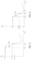
- FIG. 5 is a diagram showing a relationship between a gate-source voltage V GS1 and a source-drain current I SD1 of the first driving transistor MA2 of the light emitting unit driving circuit 100 in FIG. 2 according to an embodiment of the present disclosure
- FIG. 6 is a relationship diagram between the gate-source voltage V GS2 and the source-drain current I SD2 of the second driving transistor MB2 of the light emitting unit driving circuit 100 in FIG. 2 according to an embodiment of the present disclosure.
- FIG. 10 is another timing diagram of the lighting unit driving circuit 100C in FIG. 8 according to an embodiment of the present disclosure.
- the voltage levels of the corresponding first control lines E1[y] i.e., E[1] to E1[N]
- the voltage levels of the corresponding first control lines E1[y] may be sequentially pulled down to a low level, such that the corresponding first light emitting control transistor MA3 is turned on, and the first current Ia and the second current Ib are simultaneously flowed through the light emitting unit D.
- the bias voltages Vx1 and Vx2 are refreshed by the first data line D1[x] and the second data line D2[x] respectively.
Landscapes
- Engineering & Computer Science (AREA)
- Physics & Mathematics (AREA)
- Computer Hardware Design (AREA)
- General Physics & Mathematics (AREA)
- Theoretical Computer Science (AREA)
- Control Of Indicators Other Than Cathode Ray Tubes (AREA)
- Electroluminescent Light Sources (AREA)
Abstract
Description
- The present disclosure relates to an electronic device and a driving circuit, and more particularly to a driving circuit for driving a light emitting unit.
- With the development of digital technology, electronic devices have been widely used in various aspects of daily life. However, current electronic devices are not satisfactory in all respects.
- This in mind, the present invention aims at providing a light emitting unit driving circuit and an electronic device having the same.
- This is achieved by a light emitting unit driving circuit and an electronic device according to
claims - As will be seen more clearly from the detailed description following below, the light emitting unit driving circuit is disclosed. The light emitting unit driving circuit comprises a first driving transistor, a second driving transistor, and a light emitting unit. The first driving transistor has a first channel width and a first channel length and is configured to provide a first current. The second driving transistor has a second channel width and a second channel length and is configured to provide a second current. The light emitting unit is electrically connected to the first driving transistor and the second driving transistor and is configured to receive at least one of the first current and the second current to emit light. A first ratio of the first channel width to the first channel length is greater than a second ratio of the second channel width to the second channel length.
- The electronic device includes a light emitting unit driving circuit. The light emitting unit driving circuit comprises a first driving transistor, a second driving transistor, and a light emitting unit. The first driving transistor has a first channel width and a first channel length and is configured to provide a first current. The second driving transistor has a second channel width and a second channel length and is configured to provide a second current. The light emitting unit is electrically connected to the first driving transistor and the second driving transistor and is configured to receive at least one of the first current and the second current to emit light. A first ratio of the first channel width to the first channel length is greater than a second ratio of the second channel width to the second channel length.
- In the following, the invention is further illustrated by way of example, taking reference to the accompanying drawings. Thereof
-
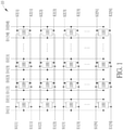
FIG. 1 is a circuit diagram of an electronic device according to an embodiment of the present disclosure; -
FIG. 2 is a circuit diagram of a light emitting unit driving circuit of the electronic device inFIG. 1 according to an embodiment of the present disclosure; -
FIG. 3 is a timing diagram of the electronic device inFIG. 1 according to an embodiment of the present disclosure; -
FIG. 4 is a top view of a first driving transistor of the light emitting unit driving circuit inFIG. 2 according to an embodiment of the present disclosure; -
FIG. 5 is a graph showing a relationship between a gate-source voltage and a source-drain current of the first driving transistor of the light emitting unit driving circuit inFIG. 2 according to an embodiment of the present disclosure; -
FIG. 6 is a graph showing a relationship between a gate-source voltage and a source-drain current of a second driving transistor of the light emitting unit driving circuit inFIG. 2 according to an embodiment of the present disclosure; -
FIGs. 7 and8 are circuit diagrams of a light emitting unit driving circuit respectively according to an embodiment of the present disclosure; -
FIG. 9 is a timing diagram of the light emitting unit driving circuit inFIG. 8 according to an embodiment of the present disclosure; -
FIG. 10 is another timing diagram of the light emitting unit driving circuit inFIG. 8 according to an embodiment of the present disclosure; and -
FIGs. 11 and12 are circuit diagrams of a light emitting unit driving circuit according to another embodiment of the present disclosure. - The terms "substantially" generally mean within 20% of a given value or range, or mean within 10%, 5%, 3%, 2%, 1%, or 0.5% of a given value or range. The quantity given here is an approximate quantity.
- In the present disclosure, "coupling" may include "electrical connection." For example, the A component "couples" the B component to include "the A component is coupled to the B component" and "the A component is electrically connected to the B component". "The A component is electrically connected to the B component" may mean that a current would flow from the A component to the B component.
-
FIG. 1 is a circuit diagram of anelectronic device 10 according to an embodiment of the present disclosure, andFIG. 2 is a circuit diagram of a light emittingunit driving circuit 100 of theelectronic device 10 inFIG. 1 according to an embodiment of the present disclosure. In an embodiment, the electronic device of the present disclosure may comprise a display device, a sensing device, an antenna device, a tiled device, a touch device, other suitable electronic devices, or a combination thereof, but is not limited thereto. Theelectronic device 10 may comprise a plurality of light emittingunit driving circuits 100, a plurality of first data lines D1 [1] to D1[M], a plurality of second data lines D2[1] to D2[M], a plurality of first scans lines S1[1] to S1[N], a plurality of second scan lines S2[1] to S2[N], a plurality of first control lines E1[1] to E1[N], and a plurality of second control lines E2[1] to E2[N]. The light emittingunit driving circuit 100 may be arranged in a matrix of M columns and N rows, and M and N may be integers greater than or equal to 2. The light emittingunit driving circuit 100 may be coupled to a corresponding first data line D1[x], a corresponding second data line D2[x], a corresponding first scan line S1[y], a corresponding second scan line S2[y], a corresponding first control line E1[y], and a corresponding second control line E2[y]. Wherein, 1≦x≦M,1≦y≦N. In an embodiment, the light emittingunit driving circuit 100 may be used to drive a light emitting unit of theelectronic device 10, but is not limited thereto. - Referring to
FIG. 2 , the light emittingunit driving circuit 100 may comprise a first driving transistor MA2, a second driving transistor MB2, and a light emitting unit D. The first terminals (e.g., the source) of the second driving transistor MB2 and the first driving transistor MA2 may be coupled to a first system voltage PVDD. The first system voltage PVDD is used to supply power to the first driving transistor MA2 and the second driving transistor MB2 to enable the first driving transistor MA2 to generate and provide a first current la, and to enable the second driving transistor MB2 to generate and provide a second current Ib. The magnitude of the first current Ia provided by the first driving transistor MA2 may be determined by a bias voltage Vx1 of the control terminal (e.g., the gate) of the first driving transistor MA2. Similarly, the magnitude of the second current Ib provided by the second driving transistor MB2 may be determined by a bias voltage Vx2 of the control terminal (e.g., the gate) of the second driving transistor MB2. Therefore, the magnitudes of the first current Ia and the second current Ib may be adjusted by adjusting the bias voltages Vx1 and Vx2. - In an embodiment of the disclosure, the light emitting
unit driving circuit 100 further comprises a first switching transistor MA1 and a second switching transistor MB1 for respectively adjusting the bias voltage Vx1 to the voltage level of the first data line D1[x], and adjusting the bias voltage Vx2 to the voltage level of the second data line D2[x]. The first switching transistor MA1 is coupled to a corresponding first data line D1[x], the first driving transistor MA2, and a corresponding first scan line S1[y]. In an embodiment, the first switching transistor MA1 is electrically connected to the first data line D1[x], the first driving transistor MA2, and the first scan line S1[y]. For example, the first terminal (e.g., one of the source and the drain) of the first switching transistor MA1 may be coupled to the corresponding first data line D1[x], and the second terminal (e.g., the other one of the source and the drain) of the first switching transistor MA1 may be coupled to a control terminal of the first driving transistor MA2, and a control terminal (e.g., the gate) of the first switching transistor MA1 may be coupled to the corresponding first scan line S1[y]. When the voltage level of the first scan line S1[y] is low, the first switching transistor MA1 is turned on, so that the first data line D1[x] is coupled to the control terminal of the first driving transistor MA2, thereby the bias voltage Vx1 is adjusted to the voltage level of the first data line D1[x]. When the voltage level of the first scan line S1[y] is high, the first switching transistor MA1 is turned off, and the bias voltage Vx1 is maintained at the original voltage level. Similarly, the second switching transistor MB1 is coupled to a corresponding second data line D2[x], the second driving transistor MB2, and a corresponding second scan line S2[y]. In an embodiment, the second switching transistor MB1 is electrically connected to the corresponding second data line D2[x], the second driving transistor MB2, and the corresponding second scan line S2[y]. For example, a first terminal (e.g., one of the source and the drain) of the second switching transistor MB1 may be coupled to the corresponding second data line D2[x], a second terminal (e.g., the other one of the source and the drain) of the second switching transistor MB1 may be coupled to a control terminal of the second driving transistor MB2, and a control terminal (e.g., the gate) of the second switching transistor MB1 may be coupled to the corresponding second scan line S2[y]. When the voltage level of the second scan line S2[y] is low, the second switching transistor MB1 is turned on, and the second data line D2[x] is coupled to the control terminal of the second driving transistor MB2, thereby the bias voltage Vx2 is adjusted to the voltage level of the second data line D2[x]. When the voltage level of the second scan line S2[y] is high, the second switching transistor MB1 is turned off, and the bias voltage Vx2 is maintained at the original voltage level. It could be understood that, in some embodiments of the present disclosure, the light emittingunit driving circuit 100 may not necessarily comprise the first switching transistor MA1 and the second switching transistor MB1. In other words, the first switching transistor MA1 and the second switching transistor MB1 are optional components, the control terminal of the first driving transistor MA2 may be directly coupled to the first scan line S1[y], and the control terminal of the second driving transistor MB2 may be directly coupled to the second scan line S2[y]. - Furthermore, the light emitting unit D may comprise, for example, an inorganic light emitting diode (LED), such as a sub-millimeter LED (mini LED) or a micro-light emitting diode (micro LED), an organic light emitting diode (OLED), quantum dot (QD), quantum dot light emitting diode (QLED, QDLED), fluorescent material, phosphor material, other suitable materials or a combination thereof, but not limited thereto. In this embodiment, one of the anode and cathode of the light emitting unit D (e.g., the anode) may be coupled to the first driving transistor MA2 and the second driving transistor MB2, and the other one of the anode and cathode of the light emitting unit D (e.g., the cathode) is coupled to the second system voltage PVSS. The second system voltage PVSS may be lower than the first system voltage PVDD. The light emitting unit D would emit light by receiving at least one of the first current Ia and the second current Ib. Further, when both the first driving transistor MA2 and the second driving transistor MB2 are turned on, the current If flowing through the light emitting unit D is equal to a sum of the first current Ia and the second current Ib (i.e., Ia+Ib). For example, when the first driving transistor MA2 is turned on and the second driving transistor MB2 is turned off, the current If flowing through the light emitting unit D may be substantially equal to the first current Ia. When the first driving transistor MA2 is turned off, and the second driving transistor MB2 is turned on, the current If flowing through the light emitting unit D may be substantially equal to the second current Ib. When both the first driving transistor MA2 and the second driving transistor MB2 are turned off, the current If flowing through the light emitting unit D is equal to zero, and the light emitting unit D would not emit light. By turning on/off of the first driving transistor MA2 and the second driving transistor MB2 as described above, the magnitude of the current If flowing through the light emitting unit D would be controlled. By changing the bias voltages Vx1 and Vx2, the operations of turning on/off the first driving transistor MA2 and the second driving transistor MB2 would be controlled.
- In an embodiment of the present disclosure, the light emitting
unit driving circuit 100 may further comprise a first light emitting control transistor MA3 and a second light emitting control transistor MB3. The first light emitting control transistor MA3 is coupled to the first driving transistor MA2 and the light emitting unit D, and is used to control whether the first current Ia flows to the light emitting unit D based on a first light emitting control signal (i.e., the voltage level of the first control line E1[y]). When the voltage level of the first control line E1[y] is low, the first light emitting control transistor MA3 is turned on, so that the first current Ia flows to the light emitting unit D. When the voltage level of the first control line E1[y] is high, the first light emitting control transistor MA3 is turned off, and the first driving transistor MA2 is electrically disconnected from the light emitting unit D, so that the first current Ia does not flow to the light unit D. Similarly, the second light emitting control transistor MB3 is coupled to the second driving transistor MB2 and the light emitting unit D, and is used to control whether the second current Ib flows to the light emitting unit D based on a second light emitting control signal (i.e., the voltage level of the second control line E2[y]). When the voltage level of the second control line E2[y] is low, the second light emitting control transistor MB3 is turned on, and the second current Ib flows to the light emitting unit D. When the voltage level of the second control line E2[y] is high, the second light emitting control transistor MB3 is turned off, and the second driving transistor MB2 is electrically disconnected from the light emitting unit D, so that the second current Ib does not flow to the light unit D. It could be understood that, in some embodiments of the present disclosure, the light emittingunit driving circuit 100 may not necessarily comprise the first light emitting control transistor MA3 and the second light emitting control transistor MB3. In other words, the first light emitting control transistor MA3 and the second light emitting control transistor MB3 are optional elements. The first driving transistor MA2 may be directly coupled to the light emitting unit D, and the second driving transistor MB2 may be directly coupled to the light emitting unit D. By controlling the operations of the first driving transistor MA2 and the second driving transistor MB2, the magnitude of the current If flowing through the light emitting unit D would be controlled. - In an embodiment of the disclosure, the light emitting
unit driving circuit 100 may further comprise a first capacitor Cgs1 and a second capacitor Cgs2. The first capacitor Cgs1 is coupled to the first terminal (e.g., the source) and the control terminal (e.g., the gate) of the first driving transistor MA2, and is used to maintain the voltage level of the bias voltage Vx1. The second capacitor Cgs2 is coupled between the first terminal (e.g., the source) and the control terminal (e.g., the gate) of the second driving transistor MB2 to maintain the voltage level of the bias voltage Vx2. In an embodiment, the first capacitor Cgs1 is electrically connected to the first driving transistor MA2. The second capacitor Cgs2 is electrically connected to the second driving transistor MB2. The capacitance of the first capacitor Cgs1 may be substantially equal to the capacitance of the second capacitor Cgs2, but is not limited thereto. It could be understood that, in some embodiments of the present disclosure, the light emittingunit driving circuit 100 may not necessarily comprise the first capacitor Cgs1 and the second capacitor Cgs2. In other words, the first capacitor Cgs1 and the second capacitor Cgs2 are optional components. -
FIG. 3 is a timing diagram of theelectronic device 10 inFIG. 1 according to an embodiment of the present disclosure. In an embodiment of the present disclosure, theelectronic device 10 would refresh the voltage levels of the first data line D1[x] and the second data line D2[x] of the light emittingunit driving circuit 100 and refresh the magnitude of the current If flowing through the light emitting unit D every time period T. In this embodiment, only one of the first current Ia and the second current Ib flows through the light emitting unit D at the same time. The time period T may comprise a first sub-period T1 and a second sub-period T2. During the first sub-period T1, the first scan lines S1[1] to S1[N] may be at a low voltage level for a period of time sequentially. When the first scan line S1[y] is at a low voltage level, the voltage level of the corresponding first data line D1[x] is written to the corresponding first driving transistor MA2 to change the corresponding bias voltage Vx1. Then, the voltage levels of the first control lines E1[1] to E1[N] are pulled down to a low voltage level, so that the corresponding first light emitting control transistor MA3 is turned on and the first current Ia flows through the light emitting unit D. Similarly, during the second sub-period T2, the second scan lines S2[1] to S2[N] are sequentially at a low voltage level for a period of time. When the second scan line S2[y] is at the low voltage level, the voltage level of the corresponding second data line D2[x] is written to the corresponding second driving transistor MB2 to change the corresponding bias voltage Vx2. Then, the voltage levels of the second control lines E2[1] to E2[N] are pulled down to the low voltage level, such that the corresponding second light emitting control transistor MB3 is turned on and the second current Ib flows through the light emitting unit D. In other embodiments, the first light emitting control transistor MA3 and the second light emitting control transistor MB3 may be controlled such that the first current Ia and the second current Ib may flow together through the light emitting unit D. - In this embodiment, the first driving transistor MA2 and the second driving transistor MB2 may be, for example, thin film transistors (TFTs), but are not limited thereto. The structure of the first driving transistor MA2 may be similar to that of the second driving transistor MB2. Hereinafter, the first driving transistor MA2 will be described as an example.
FIG. 4 is a top view of the first driving transistor MA2 of the light emittingunit driving circuit 100 inFIG. 2 according to an embodiment of the present disclosure. The first driving transistor MA2 may have agate 210, asource 250, and adrain 260. Thegate 210 may be formed on a substrate, and a gate insulating layer may be formed on thegate 210. The material of the gate insulating layer may comprise an insulating material such as silicon nitride, silicon oxide, other suitable materials, or a combination of the above materials, but is not limited thereto. Asemiconductor layer 230 may be formed on the gate insulating layer. Thesemiconductor layer 230 may comprise an amorphous semiconductor, a poly-crystalline semiconductor, a metal oxide (e.g., Indium Gallium Zinc Oxide (IGZO)), other suitable materials, or a combination of the above materials, but is not limited thereto. The first driving transistor MA2 has a channel width W and a channel length L, and the width/length ratio of the channel of the first driving transistor MA2 is defined as W/L. The width/length ratio could be obtained according to a conventional measurement method in the art, and will not be described here. The structure of the second driving transistor MB2 is similar to that of the first driving transistor MA2, and the difference between the two driving transistors MA2 and MB2 is that the width/length ratio of the second driving transistor MB2 is not equal to the width/length ratio the first driving transistor MA2. For example, the ratio of the channel width W and the channel length L of the first driving transistor MA2 is greater than the ratio of the channel width and the channel length of the second driving transistor MB2. In an embodiment of the disclosure, the channel width W of the first driving transistor MA2 may be substantially equal to 12 micrometers (µm), the channel length L of the first driving transistor MA2 may be substantially equal to 6 micrometers, and the width/length ratio of the first driving transistor MA2 is equal to 2 (i.e., 12 µm/6 µm). The channel width W of the second driving transistor MB2 may be substantially equal to 6 micrometers, the channel length L of the second driving transistor MB2 may be substantially equal to 6 micrometers, and the width/length ratio of the second driving transistor MB2 is equal to 1 (i.e., 6 µm/6 µm). It could be noted that the above dimensions are merely exemplary, and the disclosure is not limited thereto. The channel lengths and channel widths of the first driving transistor MA2 and the second driving transistor MB2 may be other sizes. - Since a transistor having a large width/length ratio could withstand a greater source-drain current than a transistor having a small width/length ratio, the first driving transistor MA2 and the second driving transistor MB2 of different width/length ratios could be used to provide the current If of different current ranges.
FIG. 5 is a diagram showing a relationship between a gate-source voltage VGS1 and a source-drain current ISD1 of the first driving transistor MA2 of the light emittingunit driving circuit 100 inFIG. 2 according to an embodiment of the present disclosure, andFIG. 6 is a relationship diagram between the gate-source voltage VGS2 and the source-drain current ISD2 of the second driving transistor MB2 of the light emittingunit driving circuit 100 inFIG. 2 according to an embodiment of the present disclosure. VGS1 represents a voltage difference between the gate and the source of the first driving transistor MA2, ISD1 represents a current flowing from the source of the first driving transistor MA2 to the drain of the first driving transistor MA2, VGS2 represents a voltage difference between the gate and the source of the second driving transistor MB2, ISD2 represents a current flowing from the source of the second driving transistor MB2 to the drain of the second driving transistor MB2. Furthermore, the gate-source voltage VGS1 is substantially equal to the voltage difference between the bias voltage Vx1 and the first system voltage PVDD and the gate-source voltage VGS2 is substantially equal to the voltage difference between the bias voltage Vx2 and the first system voltage PVDD. The source-drain current ISD1 may be substantially equal to the first current la, and the source-drain current ISD2 may be substantially equal to the second current Ib. For example, the magnitude of the current If flowing through the light emitting unit D may vary within a current range I0 to I255, so that the light emitting unit D may present 256 different values of brightness, and each value of the brightness is corresponded to one of the 256 gray levels of the light emittingunit driving circuit 100. It should be noted that the current range here is only an illustrative description. In fact, the current range and its corresponding brightness may be adjusted according to the design requirements. For example, voltage values V0, V64, V127, V128, and V255 may respectively correspond to current values I0, I64, I127, I128, and I255, and the current value I255 may be greater (or less) than current value I0. In this embodiment, the width/length ratio of the first driving transistor MA2 may be greater (or less) than the width/length ratio of the second driving transistor MB2. The first driving transistor MA2 is used to provide the first current Ia corresponding to a first current range, and the second driving transistor MB2 is used to provide the second current Ib corresponding to a second current range. The first current range may not overlap with the second current range. For example, the first current range may comprise I0 to IN, and the second current range may comprise IN+1 to I255, where N may be an integer from 1 to 253, such as 50, 100, 125, 126, 127, 128, 129 , 130, 131, 135, 150, or 175. For instance, the width/length ratio of the first driving transistor MA2 may be greater than the width/length ratio of the second driving transistor MB2, and the current value I255 may be greater than the current value I0. The first driving transistor MA2 may be used to provide the first current Ia within the current range I128 to I255, and the second driving transistor MB2 may be used to provide the second current Ib within the current range I0 to I127, but is not limited thereto. The current range I128 to I255 may not overlap with the current range I0 to I127. - One of the first light emitting control transistor MA3 and the second light emitting control transistor MB3 may be selectively turned on based on a desired magnitude of the current If, such that one of the first current Ia and the second current Ib would be equal to the current If. For example, when the desired magnitude of the current If is within the first current range, the first light emitting control transistor MA3 of the light emitting
unit driving circuit 100 is turned on. When the desired magnitude of the current If is within the second current range, the second light emitting control transistor MB3 is turned on. For instance, when the magnitude of the current If is within the current range I128 and I255, the first light emitting control transistor MA3 of the light emittingunit driving circuit 100 is turned on. When the magnitude of the current If is within the current range I0 to 1127, the second light emitting control transistor MB3 is turned on. - When the light emitting
unit driving circuit 100 starts to operate, the relationship between the gate-source voltage VGS1 and the source-drain current ISD1 of the first driving transistor MA2 may be, for example, presented by acurve 301, and the relationship between the gate voltage VGS2 and the source-drain current ISD2 of the second driving transistor MB2 may be, for example, presented by acurve 401. However, when the light emittingunit driving circuit 100 operates for a period of time, the relationship between the gate-source voltage VGS1 and the source-drain current ISD1 of the first driving transistor MA2 and the relationship between the gate voltage VGS2 and the source-drain current ISD2 of the second driving transistor MB2 may drift to be presented bycurves FIG. 5 may change from the original I128 to I128_RA, and the current value corresponding to the original voltage value V64 inFIG. 6 may change from the original I64 to I64_RA. However, since the source-drain current ISD1 of the first driving transistor MA2 is varied within the current range I0 to 1127, and the source-drain current ISD2 of the second driving transistor MB2 would be varied within the current range I128 to I255, the degree of drift using the first driving transistor MA2 and the second driving transistor MB2 may be less than the degree of drift using only a single driving transistor, which has a corresponding current range I0 to I255. - In the above embodiment, the transistors of the light emitting
unit driving circuit 100 may all be P-type transistors (as shown inFIG. 2 ), but the light emitting unit driving circuit of the present disclosure may also adopt N-type transistors.FIG. 7 is a circuit diagram of a light emittingunit driving circuit 100B according to an embodiment of the present disclosure. The first switching transistor MA1, the second switching transistor MB1, the first driving transistor MA2, the second driving transistor MB2, the first light emitting control transistor MA3, and the second light emitting control transistor MB3 may all be N-type transistors. The driving manner of the light emittingunit driving circuit 100B is similar to the driving manner of the light emittingunit driving circuit 100. The main difference between the two light emittingunit driving circuits FIG. 3 would be inversely processed to control the operations of the light emittingunit driving circuit 100B. In an embodiment, the transistors of the light emitting unit driving circuit may comprise P-type and N-type transistors. - In an embodiment of the present disclosure, one of the two transistors of the first light emitting control transistor MA3 and the second light emitting control transistor MB3 may be omitted.
FIG. 8 is a circuit diagram of a light emittingunit driving circuit 100C according to an embodiment of the present disclosure. The main difference between the light emittingunit driving circuit 100C and the light emittingunit driving circuit 100 is that the light emittingunit driving circuit 100C uses only the first light emitting control transistor MA3 to control the current If flowing to the light emitting unit D.FIG. 9 is a timing diagram of the light emittingunit driving circuit 100C inFIG. 8 according to an embodiment of the present disclosure. During the first sub-period T1, the first scan lines S1[1] to S1[N] and the second scan lines S2[1] to S2[N] may be sequentially at a low voltage level for a period of time. The data is written to the corresponding first driving transistor MA2 and the corresponding second driving transistor MB2 through the corresponding first data line D1[x] and the second data line D2[x], such that the corresponding bias voltages Vx1 and Vx2 are changed respectively. During the second sub-period T2, the voltage level of the first control line E1[y] is pulled down to a low voltage level, and the corresponding first light emitting control transistor MA3 is turned on, so that the first current Ia and the second current Ib can flow simultaneously through the light emitting unit D. -
FIG. 10 is another timing diagram of the lightingunit driving circuit 100C inFIG. 8 according to an embodiment of the present disclosure. Different from the driving method shown inFIG. 9 , in the embodiment, when the first scan line S1[y] and the second scan line S2[y] are sequentially at a low voltage level for a period of time, data is written to the corresponding first driving transistor MA2 and second driving transistor MB2 through the first data line D1[x] and the second data line D2[x] sequentially, then the voltage levels of the corresponding first control lines E1[y] (i.e., E[1] to E1[N]) may be sequentially pulled down to a low level, such that the corresponding first light emitting control transistor MA3 is turned on, and the first current Ia and the second current Ib are simultaneously flowed through the light emitting unit D. -
FIG. 11 is a circuit diagram of a light emittingunit driving circuit 100D according to another embodiment of the present disclosure. The light emittingunit driving circuit 100D is a modified version of the light emittingunit driving circuit 100 shown inFIG. 2 . InFIG. 2 , the first switching transistor MA1 and the second switching transistor MB1 are respectively coupled to the first data line D1[x] and the second data line D2[x]. However, inFIG. 11 , the switching transistor MA1 and the second switching transistor MB1 of the light emittingunit driving circuit 100D are both coupled to the first data line D1[x]. By controlling the first scan line S1[y] and the second scan line S2[y], the first switching transistor MA1 and the second switching transistor MB1 are turned on at different times. When the first switching transistor MA1 is turned on and the second switching transistor MB1 is turned off, the bias voltage Vx1 is refreshed through the first data line D1[x] while the bias voltage Vx2 is not refreshed. When the second switching transistor MB1 is turned on and the first switching transistor MA1 is turned off, the bias voltage Vx2 is refreshed through the first data line D1[x] while the bias voltage Vx1 is not refreshed. -
FIG. 12 is a circuit diagram of a light emittingunit driving circuit 100E according to another embodiment of the present disclosure. The light emittingunit driving circuit 100E is another modified version of the light emittingunit driving circuit 100 shown inFIG. 2 . InFIG. 2 , the first switching transistor MA1 and the second switching transistor MB1 are respectively coupled to the first scan line S1[y] and the second scan line S2[y]. However, inFIG. 12 , the first switching transistor MA1 and the second switching transistor MB1 of the light emittingunit driving circuit 100D are both coupled to the first scan line S1[y]. When the first scan line S1[y] is at a low voltage level to simultaneously turn on the first switching transistor MA1 and the second switching transistor MB1, the bias voltages Vx1 and Vx2 are refreshed by the first data line D1[x] and the second data line D2[x] respectively. - In summary, the first driving transistor and the second driving transistor of the light emitting unit driving circuit of the electronic device would respectively provide the first current and the second current to the light emitting unit, so that the light emitting unit may be driven by different currents. As a result, the convenience of operation may be improved. Furthermore, the first current and the second current may be respectively within different current ranges, and the electronic device would selectively turn on/off relevant transistors thereof according to the driving current required by the light emitting unit, so that the efficiency of refreshing the driving current of the light emitting unit may be improved.
- Although some embodiments of the present disclosure and their advantages have been described in detail, it should be understood that various changes, substitutions and alterations can be made herein without departing from the spirit and scope of the disclosure as defined by the appended claims. For example, it will be readily understood by one of ordinary skill in the art that many of the features, functions, processes, and materials described herein may be varied while remaining within the scope of the present disclosure. Moreover, the scope of the present application is not intended to be limited to the particular embodiments of the process, machine, manufacture, composition of matter, means, methods and steps described in the specification. As one of ordinary skill in the art will readily appreciate from the present disclosure, processes, machines, manufacture, compositions of matter, means, methods, or steps, presently existing or later to be developed, that perform substantially the same function or achieve substantially the same result as the corresponding embodiments described herein may be utilized according to the present disclosure. Accordingly, the appended claims are intended to include within their scope such processes, machines, manufacture, compositions of matter, means, methods, or steps. Moreover, each of the claims constitutes an individual embodiment, and the scope of the disclosure also includes the scope of the various claims and combinations of the embodiments. The scope of the disclosure is subject to the definition of the scope of the claims.
Claims (7)
- A light emitting unit driving circuit (100E) comprising:a first driving transistor (MA2) having a first channel width (W) and a first channel length (L) and being configured to provide a first current (Ia);a second driving transistor (MB2) having a second channel width and a second channel length and being configured to provide a second current (Ib);a light emitting unit (D) electrically connected to the first driving transistor (MA2) and the second driving transistor (MB2), and configured to receive at least one of the first current (Ia) and the second current (Ib) to emit light;characterized by further comprising:a first data line (D1[x]);a second data line (D2[x]);a scan line (S1[y]);a first switching transistor (MA1) electrically connected to the first data line (D1[x]), the first driving transistor (MA2), and the scan line (S1[y]); anda second switching transistor (MB1) electrically connected to the second data line (D2[x]), the second driving transistor (MB2), and the scan line (S1[y]); andwherein a first ratio of the first channel width (W) to the first channel length (L) is different from a second ratio of the second channel width to the second channel length.
- A light emitting unit driving circuit (100D) comprising:a first driving transistor (MA2) having a first channel width (W) and a first channel length (L) and being configured to provide a first current (Ia);a second driving transistor (MB2) having a second channel width and a second channel length and being configured to provide a second current (Ib);a light emitting unit (D) electrically connected to the first driving transistor (MA2) and the second driving transistor (MB2), and configured to receive at least one of the first current (Ia) and the second current (Ib) to emit light;characterized by further comprising:a data line (D1[x]);a first scan line (S1[y]);a second scan line (S2[y]);a first switching transistor (MA1) electrically connected to the data line (D1[x]), the first driving transistor (MA2), and the first scan line (S1[y]); anda second switching transistor (MB1) electrically connected to the data line (D1[x]), the second driving transistor (MB2), and the second scan line (S2[y]);wherein a first ratio of the first channel width (W) to the first channel length (L) is different from a second ratio of the second channel width to the second channel length.
- The light emitting unit driving circuit (100D, 100E) of claim 1 or 2, characterized by further comprising:a first light emitting control transistor (MA3) electrically connected between the first driving transistor (MA2) and the light emitting unit (D); anda second light emitting control transistor (MB3) electrically connected between the second driving transistor (MB2) and the light emitting unit (D).
- The light emitting unit driving circuit (100D, 100E) of any of claims 1 to 3, characterized by further comprising:a first capacitor (Cgsl) electrically connected to the first driving transistor (MA2); anda second capacitor (Cgs2) electrically connected to the second driving transistor (MB2).
- The light emitting unit driving circuit (100D, 100E) of claim 4, characterized in that capacitance of the first capacitor (Cgsl) is equal to the capacitance of the second capacitor (Cgs2).
- The light emitting unit driving circuit (100D, 100E) of any of claims 1 to 5, characterized in that a magnitude of the first current (Ia) is within a first current range (I128 to I255), and a magnitude of the second current (Ib) is within a second current range (I0 to I127), and the first current range (I128 to I255) does not overlap with the second current range (I0 to I127).
- An electronic device (10) characterized by comprising the light emitting unit driving circuit (100D, 100E) of any of claims 1 to 6.
Applications Claiming Priority (3)
| Application Number | Priority Date | Filing Date | Title |
|---|---|---|---|
| US201962789567P | 2019-01-08 | 2019-01-08 | |
| CN201910683440.4A CN111429834B (en) | 2019-01-08 | 2019-07-26 | Electronic device and drive circuit |
| EP20150073.3A EP3681253B1 (en) | 2019-01-08 | 2020-01-02 | Electronic device and light emitting unit driving circuit thereof |
Related Parent Applications (2)
| Application Number | Title | Priority Date | Filing Date |
|---|---|---|---|
| EP20150073.3A Division EP3681253B1 (en) | 2019-01-08 | 2020-01-02 | Electronic device and light emitting unit driving circuit thereof |
| EP20150073.3A Division-Into EP3681253B1 (en) | 2019-01-08 | 2020-01-02 | Electronic device and light emitting unit driving circuit thereof |
Publications (2)
| Publication Number | Publication Date |
|---|---|
| EP3952615A1 true EP3952615A1 (en) | 2022-02-09 |
| EP3952615B1 EP3952615B1 (en) | 2023-05-10 |
Family
ID=69104311
Family Applications (2)
| Application Number | Title | Priority Date | Filing Date |
|---|---|---|---|
| EP21199338.1A Active EP3952615B1 (en) | 2019-01-08 | 2020-01-02 | Electronic device and light emitting unit driving circuit thereof |
| EP20150073.3A Active EP3681253B1 (en) | 2019-01-08 | 2020-01-02 | Electronic device and light emitting unit driving circuit thereof |
Family Applications After (1)
| Application Number | Title | Priority Date | Filing Date |
|---|---|---|---|
| EP20150073.3A Active EP3681253B1 (en) | 2019-01-08 | 2020-01-02 | Electronic device and light emitting unit driving circuit thereof |
Country Status (2)
| Country | Link |
|---|---|
| US (1) | US11122660B2 (en) |
| EP (2) | EP3952615B1 (en) |
Families Citing this family (11)
| Publication number | Priority date | Publication date | Assignee | Title |
|---|---|---|---|---|
| CN109671398B (en) * | 2019-02-28 | 2020-05-15 | 厦门天马微电子有限公司 | Driving method of pixel driving circuit, display panel and display device |
| CN111383600B (en) * | 2020-04-28 | 2022-04-19 | 厦门天马微电子有限公司 | Pixel driving circuit, driving method, display panel and display device |
| WO2022176551A1 (en) * | 2021-02-22 | 2022-08-25 | 株式会社ジャパンディスプレイ | Display device |
| KR20230139915A (en) | 2022-03-25 | 2023-10-06 | 삼성디스플레이 주식회사 | Display device |
| CN114627804B (en) * | 2022-03-28 | 2023-08-01 | 武汉华星光电技术有限公司 | Pixel circuit and display panel |
| CN117836838A (en) * | 2022-06-14 | 2024-04-05 | 京东方科技集团股份有限公司 | Pixel circuit and driving method thereof, display panel and display device |
| KR20240040188A (en) * | 2022-09-20 | 2024-03-28 | 삼성디스플레이 주식회사 | Pixel, display device and driving method of the display device |
| KR20240043882A (en) * | 2022-09-27 | 2024-04-04 | 삼성디스플레이 주식회사 | Pixel, display device, controller and a method of driving a display device including a bias power line |
| CN116153239B (en) * | 2022-12-26 | 2025-08-15 | 深圳市洲明科技股份有限公司 | Pixel driving circuit and display device |
| US12148355B1 (en) | 2023-07-12 | 2024-11-19 | Innolux Corporation | Pixel circuit for wide brightness range display |
| CN118609506B (en) * | 2024-06-26 | 2025-11-28 | 天马新型显示技术研究院(厦门)有限公司 | Display panel and display device |
Citations (1)
| Publication number | Priority date | Publication date | Assignee | Title |
|---|---|---|---|---|
| US20180182284A1 (en) * | 2016-02-04 | 2018-06-28 | Boe Technology Group Co., Ltd. | Pixel structure, display device and driving method |
Family Cites Families (4)
| Publication number | Priority date | Publication date | Assignee | Title |
|---|---|---|---|---|
| KR101143009B1 (en) * | 2006-01-16 | 2012-05-08 | 삼성전자주식회사 | Display device and driving method thereof |
| US7808497B2 (en) | 2006-11-14 | 2010-10-05 | Wintek Corporation | Driving circuit and method for AMOLED using power pulse feed-through technique |
| KR20150004554A (en) * | 2013-07-03 | 2015-01-13 | 삼성디스플레이 주식회사 | Pixel and organic light emitting display device using the same |
| KR102420080B1 (en) * | 2017-05-19 | 2022-07-13 | 삼성디스플레이 주식회사 | Multi-channel TFT and Pixel comprising the TFT |
-
2019
- 2019-12-04 US US16/702,557 patent/US11122660B2/en active Active
-
2020
- 2020-01-02 EP EP21199338.1A patent/EP3952615B1/en active Active
- 2020-01-02 EP EP20150073.3A patent/EP3681253B1/en active Active
Patent Citations (1)
| Publication number | Priority date | Publication date | Assignee | Title |
|---|---|---|---|---|
| US20180182284A1 (en) * | 2016-02-04 | 2018-06-28 | Boe Technology Group Co., Ltd. | Pixel structure, display device and driving method |
Also Published As
| Publication number | Publication date |
|---|---|
| US11122660B2 (en) | 2021-09-14 |
| US20200221554A1 (en) | 2020-07-09 |
| EP3952615B1 (en) | 2023-05-10 |
| EP3681253A1 (en) | 2020-07-15 |
| EP3681253B1 (en) | 2021-11-03 |
Similar Documents
| Publication | Publication Date | Title |
|---|---|---|
| EP3952615B1 (en) | Electronic device and light emitting unit driving circuit thereof | |
| US12380847B2 (en) | Organic light emitting display apparatus | |
| CN111429834B (en) | Electronic device and drive circuit | |
| US11393397B2 (en) | Pixel driving circuit, pixel unit and driving method, array substrate, and display device | |
| US10134329B2 (en) | AMOLED pixel driver circuit and pixel driving method | |
| US12080229B2 (en) | Pixel driving circuit and driving method therefor, and display panel | |
| CN104008726B (en) | The image element circuit of active organic electroluminescent display and driving method thereof | |
| CN112397029A (en) | Pixel driving circuit and LTPO display panel | |
| CN111312160B (en) | Pixel driving circuit and display panel | |
| CN110473494A (en) | A kind of driving method of pixel circuit, display panel and pixel circuit | |
| CN115035858A (en) | Pixel circuit, driving method thereof and display panel | |
| EP3588480A1 (en) | Pixel driving circuit and driving method thereof, and layout structure of transistor | |
| US11183120B2 (en) | Pixel array substrate having common electrodes distributed in plurality of pixel rows and driving method thereof | |
| US11893928B2 (en) | Array substrate, and display panel and display device thereof | |
| CN111048044A (en) | Voltage programming type AMOLED pixel driving circuit and driving method thereof | |
| CN110299108B (en) | TFT compensation circuit for display device using reference current | |
| JP2025517267A (en) | PIXEL CIRCUIT, DISPLAY PANEL, DRIVING METHOD AND DISPLAY DEVICE | |
| JP2025517266A (en) | PIXEL CIRCUIT, DISPLAY PANEL, DRIVING METHOD AND DISPLAY DEVICE | |
| KR20090116402A (en) | Display device | |
| WO2020206857A1 (en) | Pixel drive circuit and display panel | |
| US20220284855A1 (en) | Display device and driving method of the same | |
| CN110070830B (en) | Pixel driving circuit and display panel | |
| CN109979395B (en) | Pixel driving circuit and display panel | |
| CN110070831B (en) | Pixel driving circuit and display panel | |
| US12293702B2 (en) | Pixel circuit and driving method therefor, display panel, and display apparatus |
Legal Events
| Date | Code | Title | Description |
|---|---|---|---|
| PUAI | Public reference made under article 153(3) epc to a published international application that has entered the european phase |
Free format text: ORIGINAL CODE: 0009012 |
|
| STAA | Information on the status of an ep patent application or granted ep patent |
Free format text: STATUS: THE APPLICATION HAS BEEN PUBLISHED |
|
| AC | Divisional application: reference to earlier application |
Ref document number: 3681253 Country of ref document: EP Kind code of ref document: P |
|
| AK | Designated contracting states |
Kind code of ref document: A1 Designated state(s): AL AT BE BG CH CY CZ DE DK EE ES FI FR GB GR HR HU IE IS IT LI LT LU LV MC MK MT NL NO PL PT RO RS SE SI SK SM TR |
|
| STAA | Information on the status of an ep patent application or granted ep patent |
Free format text: STATUS: REQUEST FOR EXAMINATION WAS MADE |
|
| 17P | Request for examination filed |
Effective date: 20220729 |
|
| RBV | Designated contracting states (corrected) |
Designated state(s): AL AT BE BG CH CY CZ DE DK EE ES FI FR GB GR HR HU IE IS IT LI LT LU LV MC MK MT NL NO PL PT RO RS SE SI SK SM TR |
|
| GRAP | Despatch of communication of intention to grant a patent |
Free format text: ORIGINAL CODE: EPIDOSNIGR1 |
|
| STAA | Information on the status of an ep patent application or granted ep patent |
Free format text: STATUS: GRANT OF PATENT IS INTENDED |
|
| RIC1 | Information provided on ipc code assigned before grant |
Ipc: G09G 3/3233 20160101ALI20221104BHEP Ipc: G09G 3/32 20160101ALI20221104BHEP Ipc: H05B 45/44 20200101AFI20221104BHEP |
|
| INTG | Intention to grant announced |
Effective date: 20221208 |
|
| GRAS | Grant fee paid |
Free format text: ORIGINAL CODE: EPIDOSNIGR3 |
|
| GRAA | (expected) grant |
Free format text: ORIGINAL CODE: 0009210 |
|
| STAA | Information on the status of an ep patent application or granted ep patent |
Free format text: STATUS: THE PATENT HAS BEEN GRANTED |
|
| AC | Divisional application: reference to earlier application |
Ref document number: 3681253 Country of ref document: EP Kind code of ref document: P |
|
| AK | Designated contracting states |
Kind code of ref document: B1 Designated state(s): AL AT BE BG CH CY CZ DE DK EE ES FI FR GB GR HR HU IE IS IT LI LT LU LV MC MK MT NL NO PL PT RO RS SE SI SK SM TR |
|
| REG | Reference to a national code |
Ref country code: GB Ref legal event code: FG4D |
|
| REG | Reference to a national code |
Ref country code: AT Ref legal event code: REF Ref document number: 1568046 Country of ref document: AT Kind code of ref document: T Effective date: 20230515 Ref country code: CH Ref legal event code: EP |
|
| REG | Reference to a national code |
Ref country code: DE Ref legal event code: R096 Ref document number: 602020010860 Country of ref document: DE |
|
| REG | Reference to a national code |
Ref country code: IE Ref legal event code: FG4D |
|
| REG | Reference to a national code |
Ref country code: LT Ref legal event code: MG9D |
|
| REG | Reference to a national code |
Ref country code: NL Ref legal event code: MP Effective date: 20230510 |
|
| REG | Reference to a national code |
Ref country code: AT Ref legal event code: MK05 Ref document number: 1568046 Country of ref document: AT Kind code of ref document: T Effective date: 20230510 |
|
| PG25 | Lapsed in a contracting state [announced via postgrant information from national office to epo] |
Ref country code: SE Free format text: LAPSE BECAUSE OF FAILURE TO SUBMIT A TRANSLATION OF THE DESCRIPTION OR TO PAY THE FEE WITHIN THE PRESCRIBED TIME-LIMIT Effective date: 20230510 Ref country code: PT Free format text: LAPSE BECAUSE OF FAILURE TO SUBMIT A TRANSLATION OF THE DESCRIPTION OR TO PAY THE FEE WITHIN THE PRESCRIBED TIME-LIMIT Effective date: 20230911 Ref country code: NO Free format text: LAPSE BECAUSE OF FAILURE TO SUBMIT A TRANSLATION OF THE DESCRIPTION OR TO PAY THE FEE WITHIN THE PRESCRIBED TIME-LIMIT Effective date: 20230810 Ref country code: NL Free format text: LAPSE BECAUSE OF FAILURE TO SUBMIT A TRANSLATION OF THE DESCRIPTION OR TO PAY THE FEE WITHIN THE PRESCRIBED TIME-LIMIT Effective date: 20230510 Ref country code: ES Free format text: LAPSE BECAUSE OF FAILURE TO SUBMIT A TRANSLATION OF THE DESCRIPTION OR TO PAY THE FEE WITHIN THE PRESCRIBED TIME-LIMIT Effective date: 20230510 Ref country code: AT Free format text: LAPSE BECAUSE OF FAILURE TO SUBMIT A TRANSLATION OF THE DESCRIPTION OR TO PAY THE FEE WITHIN THE PRESCRIBED TIME-LIMIT Effective date: 20230510 |
|
| PG25 | Lapsed in a contracting state [announced via postgrant information from national office to epo] |
Ref country code: RS Free format text: LAPSE BECAUSE OF FAILURE TO SUBMIT A TRANSLATION OF THE DESCRIPTION OR TO PAY THE FEE WITHIN THE PRESCRIBED TIME-LIMIT Effective date: 20230510 Ref country code: PL Free format text: LAPSE BECAUSE OF FAILURE TO SUBMIT A TRANSLATION OF THE DESCRIPTION OR TO PAY THE FEE WITHIN THE PRESCRIBED TIME-LIMIT Effective date: 20230510 Ref country code: LV Free format text: LAPSE BECAUSE OF FAILURE TO SUBMIT A TRANSLATION OF THE DESCRIPTION OR TO PAY THE FEE WITHIN THE PRESCRIBED TIME-LIMIT Effective date: 20230510 Ref country code: LT Free format text: LAPSE BECAUSE OF FAILURE TO SUBMIT A TRANSLATION OF THE DESCRIPTION OR TO PAY THE FEE WITHIN THE PRESCRIBED TIME-LIMIT Effective date: 20230510 Ref country code: IS Free format text: LAPSE BECAUSE OF FAILURE TO SUBMIT A TRANSLATION OF THE DESCRIPTION OR TO PAY THE FEE WITHIN THE PRESCRIBED TIME-LIMIT Effective date: 20230910 Ref country code: HR Free format text: LAPSE BECAUSE OF FAILURE TO SUBMIT A TRANSLATION OF THE DESCRIPTION OR TO PAY THE FEE WITHIN THE PRESCRIBED TIME-LIMIT Effective date: 20230510 Ref country code: GR Free format text: LAPSE BECAUSE OF FAILURE TO SUBMIT A TRANSLATION OF THE DESCRIPTION OR TO PAY THE FEE WITHIN THE PRESCRIBED TIME-LIMIT Effective date: 20230811 |
|
| PG25 | Lapsed in a contracting state [announced via postgrant information from national office to epo] |
Ref country code: FI Free format text: LAPSE BECAUSE OF FAILURE TO SUBMIT A TRANSLATION OF THE DESCRIPTION OR TO PAY THE FEE WITHIN THE PRESCRIBED TIME-LIMIT Effective date: 20230510 |
|
| PG25 | Lapsed in a contracting state [announced via postgrant information from national office to epo] |
Ref country code: SK Free format text: LAPSE BECAUSE OF FAILURE TO SUBMIT A TRANSLATION OF THE DESCRIPTION OR TO PAY THE FEE WITHIN THE PRESCRIBED TIME-LIMIT Effective date: 20230510 |
|
| PG25 | Lapsed in a contracting state [announced via postgrant information from national office to epo] |
Ref country code: SM Free format text: LAPSE BECAUSE OF FAILURE TO SUBMIT A TRANSLATION OF THE DESCRIPTION OR TO PAY THE FEE WITHIN THE PRESCRIBED TIME-LIMIT Effective date: 20230510 Ref country code: SK Free format text: LAPSE BECAUSE OF FAILURE TO SUBMIT A TRANSLATION OF THE DESCRIPTION OR TO PAY THE FEE WITHIN THE PRESCRIBED TIME-LIMIT Effective date: 20230510 Ref country code: RO Free format text: LAPSE BECAUSE OF FAILURE TO SUBMIT A TRANSLATION OF THE DESCRIPTION OR TO PAY THE FEE WITHIN THE PRESCRIBED TIME-LIMIT Effective date: 20230510 Ref country code: EE Free format text: LAPSE BECAUSE OF FAILURE TO SUBMIT A TRANSLATION OF THE DESCRIPTION OR TO PAY THE FEE WITHIN THE PRESCRIBED TIME-LIMIT Effective date: 20230510 Ref country code: DK Free format text: LAPSE BECAUSE OF FAILURE TO SUBMIT A TRANSLATION OF THE DESCRIPTION OR TO PAY THE FEE WITHIN THE PRESCRIBED TIME-LIMIT Effective date: 20230510 Ref country code: CZ Free format text: LAPSE BECAUSE OF FAILURE TO SUBMIT A TRANSLATION OF THE DESCRIPTION OR TO PAY THE FEE WITHIN THE PRESCRIBED TIME-LIMIT Effective date: 20230510 |
|
| REG | Reference to a national code |
Ref country code: DE Ref legal event code: R097 Ref document number: 602020010860 Country of ref document: DE |
|
| PLBE | No opposition filed within time limit |
Free format text: ORIGINAL CODE: 0009261 |
|
| STAA | Information on the status of an ep patent application or granted ep patent |
Free format text: STATUS: NO OPPOSITION FILED WITHIN TIME LIMIT |
|
| 26N | No opposition filed |
Effective date: 20240213 |
|
| PG25 | Lapsed in a contracting state [announced via postgrant information from national office to epo] |
Ref country code: SI Free format text: LAPSE BECAUSE OF FAILURE TO SUBMIT A TRANSLATION OF THE DESCRIPTION OR TO PAY THE FEE WITHIN THE PRESCRIBED TIME-LIMIT Effective date: 20230510 |
|
| PG25 | Lapsed in a contracting state [announced via postgrant information from national office to epo] |
Ref country code: SI Free format text: LAPSE BECAUSE OF FAILURE TO SUBMIT A TRANSLATION OF THE DESCRIPTION OR TO PAY THE FEE WITHIN THE PRESCRIBED TIME-LIMIT Effective date: 20230510 Ref country code: IT Free format text: LAPSE BECAUSE OF FAILURE TO SUBMIT A TRANSLATION OF THE DESCRIPTION OR TO PAY THE FEE WITHIN THE PRESCRIBED TIME-LIMIT Effective date: 20230510 |
|
| PG25 | Lapsed in a contracting state [announced via postgrant information from national office to epo] |
Ref country code: MC Free format text: LAPSE BECAUSE OF FAILURE TO SUBMIT A TRANSLATION OF THE DESCRIPTION OR TO PAY THE FEE WITHIN THE PRESCRIBED TIME-LIMIT Effective date: 20230510 |
|
| PG25 | Lapsed in a contracting state [announced via postgrant information from national office to epo] |
Ref country code: MC Free format text: LAPSE BECAUSE OF FAILURE TO SUBMIT A TRANSLATION OF THE DESCRIPTION OR TO PAY THE FEE WITHIN THE PRESCRIBED TIME-LIMIT Effective date: 20230510 |
|
| REG | Reference to a national code |
Ref country code: CH Ref legal event code: PL |
|
| PG25 | Lapsed in a contracting state [announced via postgrant information from national office to epo] |
Ref country code: LU Free format text: LAPSE BECAUSE OF NON-PAYMENT OF DUE FEES Effective date: 20240102 |
|
| REG | Reference to a national code |
Ref country code: DE Ref legal event code: R082 Ref document number: 602020010860 Country of ref document: DE Representative=s name: STRAUS, ALEXANDER, DIPL.-CHEM.UNIV. DR.PHIL., DE |
|
| PG25 | Lapsed in a contracting state [announced via postgrant information from national office to epo] |
Ref country code: LU Free format text: LAPSE BECAUSE OF NON-PAYMENT OF DUE FEES Effective date: 20240102 |
|
| PG25 | Lapsed in a contracting state [announced via postgrant information from national office to epo] |
Ref country code: BE Free format text: LAPSE BECAUSE OF NON-PAYMENT OF DUE FEES Effective date: 20240131 |
|
| PG25 | Lapsed in a contracting state [announced via postgrant information from national office to epo] |
Ref country code: CH Free format text: LAPSE BECAUSE OF NON-PAYMENT OF DUE FEES Effective date: 20240131 |
|
| PG25 | Lapsed in a contracting state [announced via postgrant information from national office to epo] |
Ref country code: CH Free format text: LAPSE BECAUSE OF NON-PAYMENT OF DUE FEES Effective date: 20240131 Ref country code: BE Free format text: LAPSE BECAUSE OF NON-PAYMENT OF DUE FEES Effective date: 20240131 |
|
| REG | Reference to a national code |
Ref country code: BE Ref legal event code: MM Effective date: 20240131 |
|
| PG25 | Lapsed in a contracting state [announced via postgrant information from national office to epo] |
Ref country code: BG Free format text: LAPSE BECAUSE OF FAILURE TO SUBMIT A TRANSLATION OF THE DESCRIPTION OR TO PAY THE FEE WITHIN THE PRESCRIBED TIME-LIMIT Effective date: 20230510 |
|
| PG25 | Lapsed in a contracting state [announced via postgrant information from national office to epo] |
Ref country code: BG Free format text: LAPSE BECAUSE OF FAILURE TO SUBMIT A TRANSLATION OF THE DESCRIPTION OR TO PAY THE FEE WITHIN THE PRESCRIBED TIME-LIMIT Effective date: 20230510 |
|
| PG25 | Lapsed in a contracting state [announced via postgrant information from national office to epo] |
Ref country code: IE Free format text: LAPSE BECAUSE OF NON-PAYMENT OF DUE FEES Effective date: 20240102 |
|
| PG25 | Lapsed in a contracting state [announced via postgrant information from national office to epo] |
Ref country code: IE Free format text: LAPSE BECAUSE OF NON-PAYMENT OF DUE FEES Effective date: 20240102 |
|
| PG25 | Lapsed in a contracting state [announced via postgrant information from national office to epo] |
Ref country code: CY Free format text: LAPSE BECAUSE OF FAILURE TO SUBMIT A TRANSLATION OF THE DESCRIPTION OR TO PAY THE FEE WITHIN THE PRESCRIBED TIME-LIMIT; INVALID AB INITIO Effective date: 20200102 |
|
| PG25 | Lapsed in a contracting state [announced via postgrant information from national office to epo] |
Ref country code: HU Free format text: LAPSE BECAUSE OF FAILURE TO SUBMIT A TRANSLATION OF THE DESCRIPTION OR TO PAY THE FEE WITHIN THE PRESCRIBED TIME-LIMIT; INVALID AB INITIO Effective date: 20200102 |
|
| PG25 | Lapsed in a contracting state [announced via postgrant information from national office to epo] |
Ref country code: TR Free format text: LAPSE BECAUSE OF FAILURE TO SUBMIT A TRANSLATION OF THE DESCRIPTION OR TO PAY THE FEE WITHIN THE PRESCRIBED TIME-LIMIT Effective date: 20230510 |
|
| PGFP | Annual fee paid to national office [announced via postgrant information from national office to epo] |
Ref country code: GB Payment date: 20260112 Year of fee payment: 7 |
|
| PGFP | Annual fee paid to national office [announced via postgrant information from national office to epo] |
Ref country code: DE Payment date: 20260107 Year of fee payment: 7 |
|
| PGFP | Annual fee paid to national office [announced via postgrant information from national office to epo] |
Ref country code: FR Payment date: 20260108 Year of fee payment: 7 |