EP3952151B1 - Optical add-drop multiplexing apparatus and method for controlling same - Google Patents
Optical add-drop multiplexing apparatus and method for controlling same Download PDFInfo
- Publication number
- EP3952151B1 EP3952151B1 EP20799222.3A EP20799222A EP3952151B1 EP 3952151 B1 EP3952151 B1 EP 3952151B1 EP 20799222 A EP20799222 A EP 20799222A EP 3952151 B1 EP3952151 B1 EP 3952151B1
- Authority
- EP
- European Patent Office
- Prior art keywords
- port
- microring
- filter
- input
- add
- Prior art date
- Legal status (The legal status is an assumption and is not a legal conclusion. Google has not performed a legal analysis and makes no representation as to the accuracy of the status listed.)
- Active
Links
Images





Classifications
-
- H—ELECTRICITY
- H04—ELECTRIC COMMUNICATION TECHNIQUE
- H04J—MULTIPLEX COMMUNICATION
- H04J14/00—Optical multiplex systems
- H04J14/02—Wavelength-division multiplex systems
- H04J14/0201—Add-and-drop multiplexing
- H04J14/0202—Arrangements therefor
- H04J14/0205—Select and combine arrangements, e.g. with an optical combiner at the output after adding or dropping
-
- H—ELECTRICITY
- H04—ELECTRIC COMMUNICATION TECHNIQUE
- H04J—MULTIPLEX COMMUNICATION
- H04J14/00—Optical multiplex systems
- H04J14/02—Wavelength-division multiplex systems
- H04J14/0201—Add-and-drop multiplexing
- H04J14/0202—Arrangements therefor
-
- H—ELECTRICITY
- H04—ELECTRIC COMMUNICATION TECHNIQUE
- H04J—MULTIPLEX COMMUNICATION
- H04J14/00—Optical multiplex systems
- H04J14/02—Wavelength-division multiplex systems
- H04J14/0201—Add-and-drop multiplexing
- H04J14/0202—Arrangements therefor
- H04J14/021—Reconfigurable arrangements, e.g. reconfigurable optical add/drop multiplexers [ROADM] or tunable optical add/drop multiplexers [TOADM]
-
- G—PHYSICS
- G02—OPTICS
- G02B—OPTICAL ELEMENTS, SYSTEMS OR APPARATUS
- G02B6/00—Light guides; Structural details of arrangements comprising light guides and other optical elements, e.g. couplings
- G02B6/10—Light guides; Structural details of arrangements comprising light guides and other optical elements, e.g. couplings of the optical waveguide type
- G02B6/12—Light guides; Structural details of arrangements comprising light guides and other optical elements, e.g. couplings of the optical waveguide type of the integrated circuit kind
- G02B6/12007—Light guides; Structural details of arrangements comprising light guides and other optical elements, e.g. couplings of the optical waveguide type of the integrated circuit kind forming wavelength selective elements, e.g. multiplexer, demultiplexer
-
- G—PHYSICS
- G02—OPTICS
- G02B—OPTICAL ELEMENTS, SYSTEMS OR APPARATUS
- G02B6/00—Light guides; Structural details of arrangements comprising light guides and other optical elements, e.g. couplings
- G02B6/10—Light guides; Structural details of arrangements comprising light guides and other optical elements, e.g. couplings of the optical waveguide type
- G02B6/12—Light guides; Structural details of arrangements comprising light guides and other optical elements, e.g. couplings of the optical waveguide type of the integrated circuit kind
- G02B6/12007—Light guides; Structural details of arrangements comprising light guides and other optical elements, e.g. couplings of the optical waveguide type of the integrated circuit kind forming wavelength selective elements, e.g. multiplexer, demultiplexer
- G02B6/12009—Light guides; Structural details of arrangements comprising light guides and other optical elements, e.g. couplings of the optical waveguide type of the integrated circuit kind forming wavelength selective elements, e.g. multiplexer, demultiplexer comprising arrayed waveguide grating [AWG] devices, i.e. with a phased array of waveguides
-
- G—PHYSICS
- G02—OPTICS
- G02B—OPTICAL ELEMENTS, SYSTEMS OR APPARATUS
- G02B6/00—Light guides; Structural details of arrangements comprising light guides and other optical elements, e.g. couplings
- G02B6/10—Light guides; Structural details of arrangements comprising light guides and other optical elements, e.g. couplings of the optical waveguide type
- G02B6/12—Light guides; Structural details of arrangements comprising light guides and other optical elements, e.g. couplings of the optical waveguide type of the integrated circuit kind
- G02B6/12007—Light guides; Structural details of arrangements comprising light guides and other optical elements, e.g. couplings of the optical waveguide type of the integrated circuit kind forming wavelength selective elements, e.g. multiplexer, demultiplexer
- G02B6/12009—Light guides; Structural details of arrangements comprising light guides and other optical elements, e.g. couplings of the optical waveguide type of the integrated circuit kind forming wavelength selective elements, e.g. multiplexer, demultiplexer comprising arrayed waveguide grating [AWG] devices, i.e. with a phased array of waveguides
- G02B6/12033—Light guides; Structural details of arrangements comprising light guides and other optical elements, e.g. couplings of the optical waveguide type of the integrated circuit kind forming wavelength selective elements, e.g. multiplexer, demultiplexer comprising arrayed waveguide grating [AWG] devices, i.e. with a phased array of waveguides characterised by means for configuring the device, e.g. moveable element for wavelength tuning
-
- G—PHYSICS
- G02—OPTICS
- G02B—OPTICAL ELEMENTS, SYSTEMS OR APPARATUS
- G02B6/00—Light guides; Structural details of arrangements comprising light guides and other optical elements, e.g. couplings
- G02B6/24—Coupling light guides
- G02B6/26—Optical coupling means
- G02B6/28—Optical coupling means having data bus means, i.e. plural waveguides interconnected and providing an inherently bidirectional system by mixing and splitting signals
- G02B6/293—Optical coupling means having data bus means, i.e. plural waveguides interconnected and providing an inherently bidirectional system by mixing and splitting signals with wavelength selective means
- G02B6/29331—Optical coupling means having data bus means, i.e. plural waveguides interconnected and providing an inherently bidirectional system by mixing and splitting signals with wavelength selective means operating by evanescent wave coupling
- G02B6/29332—Wavelength selective couplers, i.e. based on evanescent coupling between light guides, e.g. fused fibre couplers with transverse coupling between fibres having different propagation constant wavelength dependency
- G02B6/29334—Grating-assisted evanescent light guide couplers, i.e. comprising grating at or functionally associated with the coupling region between the light guides, e.g. with a grating positioned where light fields overlap in the coupler
-
- G—PHYSICS
- G02—OPTICS
- G02B—OPTICAL ELEMENTS, SYSTEMS OR APPARATUS
- G02B6/00—Light guides; Structural details of arrangements comprising light guides and other optical elements, e.g. couplings
- G02B6/24—Coupling light guides
- G02B6/26—Optical coupling means
- G02B6/28—Optical coupling means having data bus means, i.e. plural waveguides interconnected and providing an inherently bidirectional system by mixing and splitting signals
- G02B6/293—Optical coupling means having data bus means, i.e. plural waveguides interconnected and providing an inherently bidirectional system by mixing and splitting signals with wavelength selective means
- G02B6/29331—Optical coupling means having data bus means, i.e. plural waveguides interconnected and providing an inherently bidirectional system by mixing and splitting signals with wavelength selective means operating by evanescent wave coupling
- G02B6/29335—Evanescent coupling to a resonator cavity, i.e. between a waveguide mode and a resonant mode of the cavity
- G02B6/29338—Loop resonators
-
- G—PHYSICS
- G02—OPTICS
- G02B—OPTICAL ELEMENTS, SYSTEMS OR APPARATUS
- G02B6/00—Light guides; Structural details of arrangements comprising light guides and other optical elements, e.g. couplings
- G02B6/24—Coupling light guides
- G02B6/26—Optical coupling means
- G02B6/28—Optical coupling means having data bus means, i.e. plural waveguides interconnected and providing an inherently bidirectional system by mixing and splitting signals
- G02B6/293—Optical coupling means having data bus means, i.e. plural waveguides interconnected and providing an inherently bidirectional system by mixing and splitting signals with wavelength selective means
- G02B6/29346—Optical coupling means having data bus means, i.e. plural waveguides interconnected and providing an inherently bidirectional system by mixing and splitting signals with wavelength selective means operating by wave or beam interference
- G02B6/2935—Mach-Zehnder configuration, i.e. comprising separate splitting and combining means
- G02B6/29352—Mach-Zehnder configuration, i.e. comprising separate splitting and combining means in a light guide
- G02B6/29355—Cascade arrangement of interferometers
-
- G—PHYSICS
- G02—OPTICS
- G02B—OPTICAL ELEMENTS, SYSTEMS OR APPARATUS
- G02B6/00—Light guides; Structural details of arrangements comprising light guides and other optical elements, e.g. couplings
- G02B6/10—Light guides; Structural details of arrangements comprising light guides and other optical elements, e.g. couplings of the optical waveguide type
- G02B6/12—Light guides; Structural details of arrangements comprising light guides and other optical elements, e.g. couplings of the optical waveguide type of the integrated circuit kind
- G02B2006/12133—Functions
- G02B2006/12164—Multiplexing; Demultiplexing
-
- G—PHYSICS
- G02—OPTICS
- G02B—OPTICAL ELEMENTS, SYSTEMS OR APPARATUS
- G02B6/00—Light guides; Structural details of arrangements comprising light guides and other optical elements, e.g. couplings
- G02B6/24—Coupling light guides
- G02B6/26—Optical coupling means
- G02B6/28—Optical coupling means having data bus means, i.e. plural waveguides interconnected and providing an inherently bidirectional system by mixing and splitting signals
- G02B6/293—Optical coupling means having data bus means, i.e. plural waveguides interconnected and providing an inherently bidirectional system by mixing and splitting signals with wavelength selective means
- G02B6/29346—Optical coupling means having data bus means, i.e. plural waveguides interconnected and providing an inherently bidirectional system by mixing and splitting signals with wavelength selective means operating by wave or beam interference
- G02B6/2935—Mach-Zehnder configuration, i.e. comprising separate splitting and combining means
- G02B6/29352—Mach-Zehnder configuration, i.e. comprising separate splitting and combining means in a light guide
- G02B6/29353—Mach-Zehnder configuration, i.e. comprising separate splitting and combining means in a light guide with a wavelength selective element in at least one light guide interferometer arm, e.g. grating, interference filter, resonator
-
- G—PHYSICS
- G02—OPTICS
- G02B—OPTICAL ELEMENTS, SYSTEMS OR APPARATUS
- G02B6/00—Light guides; Structural details of arrangements comprising light guides and other optical elements, e.g. couplings
- G02B6/24—Coupling light guides
- G02B6/26—Optical coupling means
- G02B6/28—Optical coupling means having data bus means, i.e. plural waveguides interconnected and providing an inherently bidirectional system by mixing and splitting signals
- G02B6/293—Optical coupling means having data bus means, i.e. plural waveguides interconnected and providing an inherently bidirectional system by mixing and splitting signals with wavelength selective means
- G02B6/29379—Optical coupling means having data bus means, i.e. plural waveguides interconnected and providing an inherently bidirectional system by mixing and splitting signals with wavelength selective means characterised by the function or use of the complete device
- G02B6/2938—Optical coupling means having data bus means, i.e. plural waveguides interconnected and providing an inherently bidirectional system by mixing and splitting signals with wavelength selective means characterised by the function or use of the complete device for multiplexing or demultiplexing, i.e. combining or separating wavelengths, e.g. 1xN, NxM
- G02B6/29382—Optical coupling means having data bus means, i.e. plural waveguides interconnected and providing an inherently bidirectional system by mixing and splitting signals with wavelength selective means characterised by the function or use of the complete device for multiplexing or demultiplexing, i.e. combining or separating wavelengths, e.g. 1xN, NxM including at least adding or dropping a signal, i.e. passing the majority of signals
Definitions
- This application relates to the field of integrated photonic technologies, and in particular, to an optical add/drop multiplexer apparatus and a control method thereof.
- a microring resonator (MRR) structure starts to be used to build an optical add/drop multiplexer (OADM).
- OADM optical add/drop multiplexer
- a tunable range of the resonance wavelength of the MRR is required to reach about 40 nm, to cover a full C band.
- WDM wavelength division multiplexing
- a commonly used TOADM uses one or more cascaded microrings with a same waveguide size and radius to form a microring add/drop carrier filter, and the effective refractive index of the microring waveguide is changed by using a phase shifter (PS) based on the thermo-optic effect, to cover the full C band.
- PS phase shifter
- the tunable range of the MRR is determined by a free spectral range (FSR), and the FSR is inversely proportional to a microring radius.
- FSR free spectral range
- a microring radius of the TOADM should be small enough to obtain an FSR that covers the full C band.
- Such a microring radius size imposes an extremely high requirement on stability and reliability of a microring manufacturing process, increasing difficulty in microring manufacturing.
- EP 2095553 describes a method and device for hitless tunable optical filtering.
- US 2012/257130 describes a tunable wavelength filter based on a symmetric PLC circuit comprising an MZ filter-based demultiplexer, a waveguide resonator, and an MZ filter-based multiplexer.
- CN 101552648 describes a reconfigurable optical add-drop multiplexer (an ROADM structure) for realizing 16 channels with multiple orders.
- embodiments of this application provide an optical add/drop multiplexer apparatus and a control method thereof, to reduce a requirement on an FSR of a microring filter by using a band division manner, reduce a radius of the microring filter, reduce manufacturing difficulty of the microring filter, and improve reliability of the optical add/drop multiplexer apparatus.
- an embodiment of this application provides an optical add/drop multiplexer apparatus.
- the optical add/drop multiplexer apparatus is an integrated optical chip, and includes a filter unit, a waveband multiplexer/demultiplexer unit, an input port, an output port, and an add port and/or a drop port.
- the filter unit includes a plurality of microring filters, the filter unit is connected to the waveband multiplexer/demultiplexer unit, and the waveband multiplexer/demultiplexer unit is separately connected to the input port, the output port, the add port (if present), and the drop port (if present).
- the waveband multiplexer/demultiplexer unit is configured to input, based on wavelength of one or more input optical signals, the one or more input optical signals into a microring filter corresponding to a band to which the one or more input optical signals belong.
- One band corresponds to at least one microring filter, and each microring filter has a different resonance wavelength.
- the one or more input optical signals include an optical signal at the input port and/or an optical signal at the add port (if present).
- the one or more input optical signals may be the optical signal at the input port, or may be the optical signal at the add port (if present), or may include both the optical signal at the input port and the optical signal at the add port (if present).
- the filter unit is configured to couple a target optical signal from the input port to the drop port (if present), and/or couple the target optical signal from the add port (if present) to the output port.
- the target optical signal refers to an optical signal whose wavelength is equal to a resonance wavelength of the microring filter in the input optical signal.
- the waveband multiplexer/demultiplexer unit is further configured to output the target optical signal coupled to the output port and/or the drop port (if present).
- microring filters corresponding to different bands in the filter unit are used to filter the optical signal. It is easy to understand that after the bands are divided, a wavelength range corresponding to each band may be reduced. In this case, when an optical signal of each band is filtered by using the respective microring filter, a requirement on an FSR of the microring filter may be reduced, and a microring filter with a relatively large microring radius may be used. This reduces manufacturing difficulty of the microring filter, and improves reliability of the optical add/drop multiplexer apparatus.
- an optical add/drop multiplexer apparatus in three solutions are provided: Only the add port is included, only the drop port is included, or the add port and the drop port are included.
- a connection structure between the input port and the output port in the optical add/drop multiplexer apparatus is referred to as an input-output port or an input-output channel.
- a connection structure between the add port and the drop port is referred to as an add-drop port or an add-drop channel.
- the microring filter has a tunable coupler (TC), and the filter unit is specifically configured to control the microring filter to be in a working state by using the TC, and couple the target optical signal from the input port to the drop port (if present), and/or couple the target optical signal from the add port (if present) to the output port.
- TC tunable coupler
- a status (the working state and an offline state) of a microring add/drop filter may be adjusted by using the tunable coupler, to flexibly control the microring add/drop filter.
- a working band range of the microring add/drop filter may be changed by switching between the working state and the offline state.
- add-drop ports of the optical add/drop multiplexer apparatus may be connected by using a grating coupler and a directional waveguide coupler.
- the waveband multiplexer/demultiplexer unit may include a first grating coupling module, and the first grating coupling module may include the grating coupler and the waveguide directional coupler.
- a quantity of grating couplers is equal to a quantity of waveguide directional couplers, and is equal to Y, in other words, Y is equal to (A*N), where A is an integer not less than 1, N indicates a quantity of bands, and N is an integer greater than 2.
- the quantity of grating couplers and the quantity of waveguide directional couplers are equal to an integer multiple of the quantity N of bands.
- the first grating coupling module may include N grating couplers and N waveguide directional couplers.
- the first grating coupling module may include (A*N) grating couplers and (A*N) waveguide directional couplers.
- a connection relationship between the grating coupler and the waveguide directional coupler in the first grating coupling module is: A drop port of each grating coupler in the first grating coupling module is separately connected to an add port of a corresponding microring filter, and an add port of each waveguide directional coupler in the first grating coupling module is separately connected to a drop port of the corresponding microring filter.
- An input port of the first grating coupler is the add port
- an output port of an X th grating coupler is connected to an input port of an X th waveguide directional coupler
- an output port of the X th waveguide directional coupler is connected to an input port of an (X+1) th grating coupler
- an output port of a Y th waveguide directional coupler is the drop port, where X is a positive integer less than Y
- bands are divided for a to-be-added signal at the add port and a to-be-dropped signal at the drop port by using the grating coupler and the waveguide directional coupler.
- the wavelength range corresponding to each band is reduced after the bands are divided, and therefore the microring filter filters an optical signal with a relatively small wavelength range, to reduce the requirement on the FSR of the microring filter.
- the add-drop ports of the optical add/drop multiplexer apparatus may alternatively be connected by using the band pass combiner/splitter.
- the waveband multiplexer/demultiplexer unit may include a first band pass combiner/splitter and a second band pass combiner/splitter.
- a quantity of first band pass combiners/splitters is equal to a quantity of second band pass combiners/splitters, and both are equal to A.
- Each first band pass combiner/splitter includes one input port and N output ports
- each second band pass combiner/splitter includes N input ports and one output port.
- the one input port of the first band pass combiner/splitter is one add port, and one output port of the first band pass combiner/splitter is connected to an add port of one microring filter.
- the N output ports of the first band pass combiner/splitter are separately connected to add ports of N microring filters.
- the one output port of the second band pass combiner/splitter is one drop port, and one input port of the second band pass combiner/splitter is correspondingly connected to a drop port of the one microring filter.
- the N input ports of the second band pass combiner/splitter are separately connected to drop ports of the N microring filters.
- a microring filter connected to the input port of the first band pass combiner/splitter and the output port of the second band pass combiner/splitter may be a same microring filter, or may be different microring filters.
- the bands are divided for the to-be-added signal at the add port and the to-be-downloaded signal at the drop port by using a band pass combiner/splitter. After the bands are divided, the wavelength range corresponding to each band is reduced, and therefore the microring filter filters the optical signal with the relatively small wavelength range, to reduce the requirement on the FSR of the microring filter.
- the add-drop ports of the optical add/drop multiplexer apparatus are connected by using the grating coupler and the directional waveguide coupler.
- the waveband multiplexer/demultiplexer unit includes the first grating coupling module.
- the add-drop ports of the optical add/drop multiplexer apparatus are connected by using the band pass combiner/splitter.
- the waveband multiplexer/demultiplexer unit includes the band pass combiner/splitter.
- input-output ports of the optical add/drop multiplexer apparatus may be connected by using the grating coupler.
- one add-drop channel is used as an example to describe the connection structure of the input-output port of the optical add/drop multiplexer apparatus by using the grating coupler.
- the waveband multiplexer/demultiplexer unit includes the first grating coupling module.
- the waveband multiplexer/demultiplexer unit may include a second grating coupling module.
- the second grating coupling module includes a grating coupler, and a quantity of grating couplers in the second grating coupling module is equal to the quantity N of bands, where N is an integer not less than 2.
- A is equal to 1, and one band corresponds to one microring filter.
- the filter unit includes the N microring filters, and one grating coupler in the second grating coupling module corresponds to one microring filter.
- a connection relationship between the microring filter and the grating coupler is: In the second grating coupling module, a drop port of each grating coupler is separately connected to an input port of a corresponding microring filter, and an add port of each grating coupler is separately connected to an output port of the corresponding microring filter.
- An input port of a first grating coupler is the input port
- an output port of an M th grating coupler is coupled to an input port of an (M+1) th grating coupler
- an output port of an N th grating coupler is the output port, where M is an integer not greater than N.
- a plurality of add-drop channels are used as an example to describe the connection structure of the input-output port of the optical add/drop multiplexer apparatus by using the grating coupler.
- the waveband multiplexer/demultiplexer unit includes the first grating coupling module.
- the waveband multiplexer/demultiplexer unit may include a second grating coupling module.
- the second grating coupling module includes a grating coupler, and a quantity of grating couplers in the second grating coupling module is equal to the quantity N of bands, where N is an integer not less than 2.
- A is an integer greater than 1
- A is a quantity of add-drop channels
- one band corresponds to the plurality of microring filters.
- the filter unit includes (A*N) microring filters, and one grating coupler in the second grating coupling module corresponds to A microring filters.
- a drop port of each grating coupler is separately connected to an input port of a first microring filter in the A corresponding microring filters, and an add port of each grating coupler is separately connected to an output port of an A th microring filter in the A corresponding microring filters.
- An input port of a first grating coupler is the input port
- an output port of an M th grating coupler is coupled to an input port of an (M+1) th grating coupler
- an output port of an N th grating coupler is the output port, where M is an integer not greater than N.
- an output port of an X th microring filter is connected to an input port of an (X+1) th microring filter, where X is an integer not less than 1.
- the input-output ports of the optical add/drop multiplexer apparatus may be connected by using the band pass combiner/splitter.
- one add-drop channel is used as an example to describe a connection structure of a band pass combiner/splitter that may be used between input-output ports of the optical add/drop multiplexer apparatus.
- the waveband multiplexer/demultiplexer unit includes the first grating coupling module.
- the waveband multiplexer/demultiplexer unit may further include a third band pass combiner/splitter and a fourth band pass combiner/splitter.
- the third band pass combiner/splitter includes one input port and N output ports
- the fourth band pass combiner/splitter includes N input ports and one output port.
- A is equal to 1
- one band corresponds to one microring filter.
- the filter unit includes the N microring filters, and the input port of the third band pass combiner/splitter is the input port.
- the N output ports of the third band pass combiner/splitter are separately connected to input ports of the N microring filters, output ports of the N microring filters are separately connected to the N input ports of the fourth band pass combiner/splitter, and the output port of the fourth band pass combiner/splitter is the output port.
- a plurality of add-drop channels are used as an example to describe a connection structure of a band pass combiner/splitter that may be used between input-output ports of the optical add/drop multiplexer apparatus.
- the waveband multiplexer/demultiplexer unit includes the first grating coupling module.
- the waveband multiplexer/demultiplexer unit including the first band pass combiner/splitter and the second band pass combiner/splitter may further include a third band pass combiner/splitter and a fourth band pass combiner/splitter.
- the third band pass combiner/splitter includes one input port and N output ports
- the fourth band pass combiner/splitter includes N input ports and one output port.
- A is an integer greater than 2
- A is a quantity of add-drop channels
- one band corresponds to the plurality of microring filters.
- the filter unit includes (A*N) microring filters, and the input port of the third band pass combiner/splitter is the input port.
- One output port of the third band pass combiner/splitter and one input port of the fourth band pass combiner/splitter correspond to A same microring filters.
- Each output port of the third band pass combiner/splitter is connected to an input port of a first microring filter in the A corresponding microring filters
- each input port of the fourth band pass combiner/splitter is connected to an output port of an A th microring filter in the A corresponding microring filters
- the output port of the fourth band pass combiner/splitter is the output port.
- an output port of an X th microring filter is connected to an input port of an (X+1) th microring filter, where X is an integer not less than 1.
- the filter unit is further configured to adjust a resonance wavelength of the first microring filter to be equal to a resonance wavelength of a second microring filter.
- the waveband multiplexer/demultiplexer unit is further configured to adjust a working band of a waveguide directional coupler corresponding to the first microring filter from a band corresponding to the first microring filter to a band corresponding to the second microring filter, to back up a target optical signal corresponding to the second microring filter by using the first microring filter.
- Both the first microring filter and the second microring filter may be one or more filters in the filter unit.
- the working band range of the waveguide directional coupler may be changed, so that sub-optical paths corresponding to the microring filters serve as mutual backup. If a microring add/drop filter in one group of optical paths fails, a wavelength signal may be transmitted through a backup sub-optical path by changing the working band range of the directional coupler. Finally, a wavelength add/drop function is implemented by using a microring filter with a tunable resonance wavelength.
- either of the add port and/or the drop port is connected to a wedge-shaped waveguide, or is connected to an anti-reflection waveguide or a blocking waveguide that is based on an absorbing material.
- a waveguide corresponding to one of the add port and the drop port of the microring filter is a wedge-shaped waveguide, or an anti-reflection waveguide or a blocking waveguide that is based on an absorbing material.
- the add port or the drop port may alternatively be suspended (not connected to any waveguide).
- the foregoing technical solution may allow the add port or the drop port to have a high-loss structure having an anti-reflection function, and therefore a corresponding optical signal add/drop function cannot be implemented. It may be considered that the add port or the drop port exists but is unavailable, or it may be considered that the add port or the drop port does not exist.
- the grating coupler includes but is not limited to a grating-assisted directional coupler and/or a grating-assisted contra-directional coupler.
- all grating couplers in the first grating coupling module may be grating-assisted directional couplers.
- all the grating couplers in the first grating coupling module may be grating-assisted contra-directional couplers.
- the band pass splitter includes but is not limited to a cascaded Mach-Zehnder interferometer and/or a wavelength-insensitive directional coupling element.
- the wavelength-insensitive directional coupling element includes but is not limited to a wavelength-insensitive power splitter (PS) and a wavelength-insensitive waveguide directional coupler.
- the PS may include a cascaded star splitter (SS) and a Y-branch splitter (Y-branch).
- the microring filter may include but is not limited to a microring add/drop filter with a TC.
- an embodiment of this application provides a control method for an optical add/drop multiplexer apparatus, including: inputting, based on wavelength of one or more input optical signals, the one or more input optical signals into a microring filter corresponding to a band to which the one or more input optical signals belong, where one band corresponds to at least one microring filter, each microring filter has a different resonance wavelength, and the one or more input optical signals include an optical signal at an input port and/or an add port; coupling a target optical signal from the input port to a drop port, and/or coupling a target optical signal from the add port to an output port, where the target optical signal is an optical signal whose wavelength is equal to a resonance wavelength of the microring filter in the input optical signal; and outputting the target optical signal coupled to the output port and/or the drop port.
- the microring filter has a TC
- the method specifically includes: controlling, by using the TC, the microring filter to be in a working state, and coupling the target optical signal from the input port to the drop port, and/or coupling the target optical signal from the add port to the
- control method for the optical add/drop multiplexer apparatus further includes: adjusting a resonance wavelength of a first microring filter to be equal to a resonance wavelength of a second microring filter; and adjusting a working band of a second coupler corresponding to the first microring filter from a band corresponding to the first microring filter to a band corresponding to the second microring filter, to back up a target optical signal corresponding to the second microring filter by using the first microring filter.
- Both the first microring filter and the second microring filter may be one or more filters in a filter unit.
- control method for the optical add/drop multiplexer apparatus further includes: controlling, by using the TC, the microring filter to be in an offline state, and coupling the one or more input optical signals from the input port to the output port, or coupling the one or more input optical signals from the add port to the drop port; and outputting the one or more input optical signals coupled to the output port and/or the drop port.
- the optical add/drop multiplexer apparatus may further switch between different wavelengths in a band corresponding to a same microring filter.
- the control method for the optical add/drop multiplexer apparatus further includes: controlling the microring filter to be in the offline state, adjusting a resonance wavelength of the microring filter from a first wavelength to a second wavelength, and controlling the microring filter to be in the working state after the adjustment is completed, where both the first wavelength and the second wavelength belong to the band corresponding to the microring filter.
- the optical add/drop multiplexer apparatus may further switch between wavelengths in bands corresponding to different microring filters.
- the control method of the optical add/drop multiplexer apparatus further includes: controlling a third microring filter to be in the offline state, where a resonance wavelength of the third microring filter is the first wavelength; controlling a fourth microring filter to be in the offline state, and configuring a resonance wavelength of the fourth microring filter as the second wavelength; and keeping the third microring filter in the offline state, and switching the fourth microring filter to the working state.
- an embodiment not according to the claimed invention further provides an integrated optical chip, and the optical add/drop multiplexer apparatus according to any one of the first aspect or the implementations of the first aspect is integrated into the integrated optical chip.
- the integrated optical chip may be integrated into a system-on-a-chip SoC.
- Embodiments of this application provide an optical add/drop multiplexer apparatus and a control method thereof, to reduce a microring radius by using a band division manner, reduce manufacturing difficulty of a microring filter, and improve reliability of the optical add/drop multiplexer apparatus.
- “Waveband” and “band” in following descriptions have a same meaning, and “and/or” means that at least one of the items is included.
- “A and/or B” may be A, may be B, or may be A and B.
- the "working state” in the embodiments of this application may be referred to as an “online state” or an “on state”.
- the “non-working state” may be referred to as an "offline state” or an “off state”.
- FIG. 1 is a schematic diagram of a structure of an OADM according to an embodiment of this application.
- the OADM 100 is an integrated optical chip, and the OADM 100 may include a filter unit 101, a waveband multiplexer/demultiplexer unit 102, an input port 103, an output port 104, an add port 105, and/or a drop port 106.
- the OADM 100 may include the add port 105 or the drop port 106, namely, to form a three-port OADM.
- the OADM 100 may also include the add port and the drop port, namely, to form a four-port OADM.
- a design may be performed according to an actual requirement. This is not limited in this application.
- the waveband multiplexer/demultiplexer unit 102 is configured to input, based on wavelength of one or more input optical signals, the one or more input optical signals into a microring filter corresponding to a band to which the one or more input optical signals belong.
- One band corresponds to at least one microring filter, and each microring filter has a different resonance wavelength.
- the one or more input optical signals include an optical signal at the input port 103 and/or the add port 105.
- the one or more input optical signals may be an optical signal at the input port 103, or may be an optical signal at the add port 105, or may include both the optical signal at the input port 103 and the optical signal at the add port 105.
- the filter unit 101 is configured to control the microring filter to be in a working state, and couple the target optical signal from the input port 103 to the drop port 106, and/or couple the target optical signal from the add port 105 to the output port 104.
- the target optical signal is an optical signal whose wavelength is equal to a resonance wavelength of the microring filter in the input optical signal.
- the waveband multiplexer/demultiplexer unit 102 is further configured to output the target optical signal coupled to the output port 104 and/or the drop port 106.
- connection structure between the input port and the output port in the OADM may be referred to as an input-output port or an input-output channel.
- a connection structure between the add port and the drop port may be referred to as an add-drop port or an add-drop channel.
- the add-drop channel of the OADM 100 can be designed by using a serial solution or a parallel solution.
- the add-drop channel of the OADM 100 may specifically include a grating coupler and a directional waveguide coupler.
- the waveband multiplexer/demultiplexer unit 102 may include a first grating coupling module.
- the first grating coupling module may include the grating coupler and the waveguide directional coupler.
- a quantity of grating couplers is equal to a quantity of waveguide directional couplers and is equal to Y, where Y is equal to (A*N), A is an integer not less than 1, N indicates a quantity of bands, and N is an integer greater than 2.
- a connection relationship between the grating coupler, the waveguide directional coupler, and the microring filter in the OADM 100 is specifically as follows: A drop port of each grating coupler in the first grating coupling module is separately connected to an add port of a corresponding microring filter, and an add port of each waveguide directional coupler in the first grating coupling module is separately connected to a drop port of the corresponding microring filter.
- An input port of the first grating coupler is the add port 105
- an output port of an X th grating coupler is connected to an input port of an X th waveguide directional coupler
- an output port of the X th waveguide directional coupler is connected to an input port of an (X+1) th grating coupler
- an output port of a Y th waveguide directional coupler is the drop port 106, where X is a positive integer less than Y
- a wedge-shaped waveguide, or an anti-reflection waveguide or a blocking waveguide that is based on an absorbing material may be disposed at a specific port of the microring filter.
- the waveguide mentioned above may be disposed at a drop port of each microring filter of the OADM 100.
- a design manner of an optical add/drop multiplexer apparatus having only a drop function includes:
- the wedge-shaped waveguide, or the anti-reflection waveguide or the blocking waveguide that is based on the absorbing material is disposed as a waveguide (namely, an add waveguide) corresponding to an add port of each microring filter in the optical add/drop multiplexer apparatus 100.
- a waveguide namely, an add waveguide
- the foregoing three-port design solution is applicable to OADMs with one or more add-drop channels.
- the add port or the drop port may alternatively be suspended (not connected to any waveguide).
- the foregoing technical solution may allow the add port or the drop port to be a high-loss structure having an anti-reflection function, and therefore an optical signal add/drop function cannot be implemented. It may be considered that the add port or the drop port exists but is unavailable, or it may be considered that the add port or the drop port does not exist.
- the add-drop channel of the optical add-drop multiplexer apparatus 100 may be formed by connecting band pass combiners/splitters.
- the waveband multiplexer/demultiplexer unit 102 may include a first band pass combiner/splitter and a second band pass combiner/splitter.
- a quantity of first band pass combiners/splitters is equal to a quantity of second band pass combiners/splitters, and both are equal to A.
- Each first band pass combiner/splitter includes one input port and N output ports, and each second band pass combiner/splitter includes N input ports and one output port.
- the one input port of the first band pass combiner/splitter is the add port 105.
- One output port of the first band pass combiner/splitter is connected to an add port of one microring filter.
- the N output ports of the first band pass combiner/splitter are separately connected to add ports of N microring filters.
- the one output port of the second band pass combiner/splitter is the drop port 106.
- One input port of the second band pass combiner/splitter is correspondingly connected to a drop port of the one microring filter.
- the N input ports of the second band pass combiner/splitter are separately connected to drop ports of the N microring filters.
- the grating coupler may be used to perform serial connection between input-output ports of the OADM.
- the waveband multiplexer/demultiplexer unit 102 may further include a second grating coupling module.
- the second grating coupling module includes a grating coupler.
- a quantity of grating couplers is equal to the quantity N of the bands.
- one band corresponds to one microring filter
- the filter unit 101 includes the N microring filters.
- One grating coupler in the second grating coupling module corresponds to one microring filter.
- a connection relationship between the microring filter and the grating coupler is as follows: A drop port of each grating coupler is separately connected to an input port of a corresponding microring filter. An add port of each grating coupler is separately connected to an output port of the corresponding microring filter.
- An input port of a first grating coupler is the input port 103.
- An output port of an M th grating coupler is coupled to an input port of an (M+1) th grating coupler.
- An output port of an N th grating coupler is the output port 104, where M is an integer not greater than N.
- the filter unit 101 includes (A*N) microring filters.
- One grating coupler in the second grating coupling module corresponds to A microring filters.
- a drop port of each grating coupler in the second grating coupling module is connected to an input port of a first microring filter in the A corresponding microring filters.
- An add port of each grating coupler is separately connected to an output port of an A th microring filter in the A corresponding microring filters.
- An input port of a first grating coupler is the input port 103.
- the output port of the M th grating coupler is coupled to the input port of the (M+1) th grating coupler.
- the output port of the N th grating coupler is the output port 104, where M is an integer not greater than N.
- an output port of an X th microring filter is connected to an input port of an (X+1) th microring filter, where X is an integer not less than 1.
- the input-output ports of the OADM may be connected in parallel by using the band pass combiner/splitter.
- the waveband multiplexer/demultiplexer unit 102 may further include a third band pass combiner/splitter and a fourth band pass combiner/splitter.
- the third band pass combiner/splitter includes one input port and N output ports
- the fourth band pass combiner/splitter includes N input ports and one output port.
- the filter unit 101 includes the N microring filters.
- the input port of the third band pass combiner/splitter is the input port 103, and the N output ports of the third band pass combiner/splitter are separately connected to input ports of the N microring filters.
- Output ports of the N microring filters are respectively connected to the N input ports of the fourth band pass combiner/splitter, and the output port of the fourth band pass combiner/splitter is the output port 104.
- A is an integer greater than 1, namely, A is the quantity of add-drop channels, and one band corresponds to the plurality of microring filters.
- the filter unit 101 includes the (A*N) microring filters.
- the input port of the third band pass combiner/splitter is the input port 103, and one output port of the third band pass combiner/splitter and one input port of the fourth band pass combiner/splitter correspond to A same microring filters.
- Each output port of the third band pass combiner/splitter is connected to an input port of a first microring filter in the A microring filters corresponding to the third band pass combiner/splitter.
- Each input port of the fourth band pass combiner/splitter is connected to an output port of an A th microring filter in the A microring filters corresponding to the fourth band pass combiner/splitter.
- the output port of the fourth band pass combiner/splitter is the output port 104.
- an output port of an X th microring filter is connected to an input port of an (X+1) th microring filter, where X is an integer not less than 1.
- the filter unit is further configured to adjust a resonance wavelength of the first microring filter to be equal to a resonance wavelength of a second microring filter.
- the waveband multiplexer/demultiplexer unit is further configured to adjust a working band of a waveguide directional coupler corresponding to the first microring filter from a band corresponding to the first microring filter to a band corresponding to the second microring filter, to back up a target optical signal corresponding to the second microring filter by using the first microring filter.
- Both the first microring filter and the second microring filter may be one or more filters in the filter unit.
- the filter unit includes eight microring filters (numbered 1 to 8). The first microring filter is an odd-numbered microring filter, and the second microring filter is an even-numbered microring filter.
- the grating coupler includes but is not limited to a grating-assisted directional coupler and/or a grating-assisted contra-directional coupler.
- all the grating couplers in the first grating coupling module may be grating-assisted directional couplers.
- all the grating couplers in the first grating coupling module may be grating-assisted contra-directional couplers.
- the two types of couplers are used together.
- the band pass splitter includes but is not limited to a cascaded Mach-Zehnder interferometer and/or a wavelength-insensitive directional coupling element.
- the wavelength-insensitive directional coupling element includes but is not limited to a wavelength-insensitive power splitter (PS) and a wavelength-insensitive waveguide directional coupler.
- the PS may be a cascaded star splitter star splitter and a Y-branch splitter Y-branch.
- the microring filter may be a microring add/drop filter (ADF) with a tunable coupler (TC).
- ADF microring add/drop filter
- TC tunable coupler
- the ADF with the TC is different in that the ADF can be controlled to be in a working or an offline state by using the TC. In the working state, the ADF generates a filter effect on an optical signal input into the ADF.
- the ADF filters, to a microring, an optical signal whose wavelength is equal to a resonance wavelength of the microring in the input optical signal, so that the optical signal can be coupled from one waveguide to another waveguide.
- an input-output waveguide is coupled to an add-drop waveguide, and/or the add-drop waveguide is coupled to the input-output waveguide.
- the ADF does not filter the optical signal input into the ADF. It should be noted that one port of the input-output waveguide is the input port 103, and the other port is the output port 104. One port of the add-drop waveguide is the add port 105, and the other port is the drop port 106.
- band division may reduce a band range corresponding to each band.
- a requirement on an FSR of the microring filter may be reduced.
- the OADM may use a microring filter with a relatively large microring radius, to reduce manufacturing difficulty of the microring filter, and improve reliability of the optical add/drop multiplexer apparatus.
- FIG. 2 is a schematic diagram of a structure of a first OADM and a second OADM according to an embodiment of this application.
- a serial solution design is used for an input-output port and an add-drop port.
- an add-drop port in an OADM includes a grating coupler and a directional waveguide coupler
- an input-output port of the OADM includes a grating coupler.
- the serial solution design is used for the input-output port
- a parallel solution design is used for the add-drop port.
- the add-drop port of the OADM is formed by the grating coupler and the directional waveguide coupler
- the input-output port of the OADM is formed by a band pass combiner/splitter.
- the OADM 200 in the first OADM architecture includes an input port 201, an output port 202, an add port 203, a drop port 204, a filter unit 205, a grating coupling module 207, and a grating coupling module 206.
- the grating coupling module 206 includes a plurality of grating couplers.
- the grating coupling module 207 includes a plurality of grating couplers and a waveguide directional coupler.
- the waveband multiplexer/demultiplexer unit 102 in FIG. 1 may specifically include the grating coupling module 206 and the grating coupling module 207 shown in FIG. 2 .
- a quantity of grating couplers in the grating coupling module 206 is equal to a quantity of divided bands.
- the grating coupling module 206 is the second grating coupling module in the waveband multiplexer/demultiplexer unit 102 in FIG. 1 .
- a quantity of grating couplers in the grating coupling module 207 is equal to a quantity of waveguide directional couplers, and is equal to a quantity of microring filters in the filter unit 205.
- the grating coupling module 207 is the first grating coupling module in the waveband multiplexer/demultiplexer unit 102 in FIG. 1 .
- the OADM 200 in the second OADM architecture includes the input port 201, the output port 202, the add port 203, the drop port 204, the filter unit 205, the grating coupling module 206, a band pass combiner/splitter 208, and a band pass combiner/splitter 209.
- the waveband multiplexer/demultiplexer unit 102 in FIG. 1 specifically includes the grating coupling module 206 shown in FIG. 2 , the band pass combiner/splitter 208, and the band pass combiner/splitter 209.
- a quantity of output ports of the band pass combiner/splitter 208 and a quantity of input ports of the band pass combiner/splitter 209 are both equal to the quantity of divided bands.
- a quantity of the band pass combiners/splitters 208 and a quantity of the band pass combiners/splitters 209 are both equal to a quantity of add-drop channels.
- the band pass combiner/splitter 208 is the third band pass combiner/splitter located at the add port of the waveband multiplexer/demultiplexer unit 102 in FIG. 1 .
- the band pass combiner/splitter 209 is the fourth band pass combiner/splitter located at the drop port of the waveband multiplexer/demultiplexer unit 102 in FIG. 1 .
- the first OADM architecture for a connection relationship between the add port 203 and the drop port 204, refer to related descriptions in the embodiment in which the add port and the drop port use the grating coupler and the directional waveguide coupler in FIG. 1 . Details are not described herein again.
- the second OADM architecture for a connection relationship between the add port 203 and the drop port 204, refer to related descriptions in the embodiment in which the add port and the drop port use the band pass combiner/splitter. Details are not described herein again.
- connection manner between the input port 201 and the output port 202 may be specifically the single-channel and multi-channel serial connection manner described in FIG. 1 .
- the quantity of microring filters in the filter unit 205 is equal to the quantity N of bands.
- the quantity of microring filters in the filter unit 205 is A times the quantity of bands, where A is an integer greater than 1.
- Single-channel and multi-channel refer to one or more add-drop channels. A change in the quantity of add-drop channels does not lead to a change in a structure of each add-drop channel, but leads to a difference in a connection structure between the add-drop channel and an input-output channel. For details, refer to related descriptions in the embodiments in FIG. 3(a) and FIG. 5 . Details are not described herein again.
- the OADM architectures use an ADF with a tunable coupler TC to divide a C band in a 32 nm wavelength range.
- FIG. 3(a) is a schematic diagram of a structure of a single-channel TOADM apparatus in a first OADM architecture according to an embodiment of this application.
- the TOADM includes grating-assisted directional couplers (GADC) 301 to 304, 313 to 316, ADFs 305 to 308, waveguide directional couplers 309 to 312, an input port 317, an output port 318, a drop port 319, and an add port 320.
- GDC grating-assisted directional couplers
- the GADC has four ports (Gi, Gd, Go, and Ga).
- an optical path direction is as follows: A signal is input from Gi, a signal whose signal wavelength is in a GADC band range is transmitted to Gd, and other optical signals are transmitted to Go. A signal is input from the Ga, a signal whose signal wavelength is in the GADC band range is transmitted to Go, and other signals are transmitted to Gd.
- a C band in a 32 nm wavelength range is divided into four sub-bands at a granularity of 0.1 nm.
- Each sub-band includes optical signals of 20 wavelengths, and the four sub-bands separately correspond to the ADFs 305 to 308.
- FIG. 3(b) shows connection relationships between the GADC 301, the GADC 313, the ADF 305, and the waveguide directional coupler 309.
- a drop port of the GADC 301 is connected to an input port of the ADF 305
- an add port of the GADC 301 is connected to an output port of the ADF 305
- an add port of the ADF 305 is connected to a drop port of the GADC 313
- a drop port of the ADF 305 is connected to an add port of the GADC 313
- an output port of the GADC 313 is connected to an input port of the waveguide directional coupler 309.
- 3(b) of the tunable optical add/drop multiplexer TOADM in FIG. 3(a) may be considered as one group of add-drop sub-optical paths, and four groups of sub-optical paths form one add-drop port of the optical add/drop multiplexer.
- Working principles of drop, add, and pass-through processes of the optical add/drop multiplexer are as follows.
- Drop process A to-be-dropped signal ⁇ i entering from the input port 317 is transmitted along an input-output waveguide. It is assumed that ⁇ i is in a wavelength selection range of the grating-assisted directional coupler 302, the signal ⁇ i directly passes through the grating-assisted directional coupler 301, and enters a second group of add-drop sub-optical paths (namely, the ADF 306) through the grating-assisted directional coupler 302. The ADF 306 is in a working state, and a resonance wavelength of the ADF 306 is configured at ⁇ i .
- the signal ⁇ i is dropped by the ADF 306 to a port d2, and is transmitted to the drop port 319 along an add-drop waveguide.
- a wavelength selection range of the GADC 313 at a1 is the same as that of the GADC 301.
- the signal ⁇ i passes through the GADC 313, and is output at the drop port 319. Because remaining wavelength signals that are in the wavelength selection range of the GADC 302 do not meet a resonance condition of the GADC 302, and therefore the remaining wavelength signals pass through the ADF 306, and are coupled back to the input-output waveguide by the GADC 302 for forward transmission.
- ⁇ j enters from the input port 317. It is assumed that a band range of ⁇ j corresponds to the band range of the GADC 303, a wavelength signal of ⁇ j needs to pass through the current TOADM, and then go to a next station.
- the signal ⁇ j passes through the GADCs 301 and 302, and enters a third group of add-drop sub-optical paths (namely, the ADF 307) through the GADC 303.
- the ADF 307 is configured to be in an offline "OFF" state, and the signal ⁇ j directly passes through the ADF 307. After passing through the GADC 303, the signal returns to the input-output waveguide, directly passes through the GADC 304, and then is output from the output port 318.
- a to-be-added signal ⁇ ' i enters from the add port 320.
- the ADF306 is in the working state, and the resonance wavelength of the ADF 306 is configured at ⁇ i .
- the signal ⁇ ' i is added by the ADF 306 and is output by the GADC 302 to the input-output waveguide for transmission toward the output port 318. Because ⁇ ' i is not in wavelength selection ranges of the GADCs 303 and 304, the signal ⁇ ' i directly passes through the GADCs 303 and 304, and is output from the output port 318.
- the ADFs 305 to 308, the GADCs 309 to 312, and the waveguide directional couplers 313 to 316 together form one add-drop channel of the TOADM, which is used to add/drop a wavelength ⁇ x .
- Only one ADF corresponding to a band in which ⁇ x is located is in an ON state, and a resonance wavelength of the ADF is configured at ⁇ x .
- the other three ADFs are all in the OFF state.
- the ON/OFF state of the ADF and the resonance wavelength of the ADF in the ON state are changed to switch add/drop wavelengths.
- the working state or the offline state of the ADF may be controlled by using an electro-optic effect or a thermo-optic effect.
- the GADCs 301 to 304 and the GADCs 313 to 316 are both GADCs.
- all or some of the GADCs 301 to 304 and the GADCs 313 to 316 may be replaced with grating-assisted contra-directional couplers (GACDC).
- GCDC grating-assisted contra-directional couplers
- Working principles of the two grating couplers are the same.
- a connection structure of a replaced TOADM is similar to that in FIG. 3(a) . Details are not described herein again. A difference lies in that positions of Ga and Gd of the replaced grating coupler are exchanged, and the direction of the optical path connected to the ports of the TOADM needs to be changed accordingly.
- a wavelength selection range of the waveguide directional coupler is determined based on a grating structure.
- the waveguide directional coupler works normally, there is no need to perform active switching control. However, if a thin film heater is used to heat a grating region of the waveguide directional coupler, a refraction coefficient of the waveguide directional coupler changes, and a working range of the waveguide directional coupler may be changed.
- the four groups of add-drop sub-optical paths shown in FIG. 3(a) in the waveguide directional coupler serve as mutual backup. If an ADF in one group of sub-optical paths fails, the working range of the waveguide directional coupler may be changed, so that the wavelength signal is transmitted through a backup sub-optical path, to implement backup with an ADF with a tunable resonance wavelength.
- FIG. 4 is a schematic diagram of a structure of a single-channel TOADM apparatus in a second OADM architecture according to an embodiment of this application.
- the TOADM shown in FIG. 4 includes GADCs 401 to 404, ADFs 405 to 408, a band pass combiner (BPC) 409, a band pass splitter (BPS) 410, an output port 411, an output port 412, an add port 413, and a drop port 414.
- BPC band pass combiner
- BPS band pass splitter
- Structures and functions of the grating-assisted directional couplers 401 to 404 and the microring add/drop filters 405 to 408 in the TOADM shown in FIG. 4 are separately similar to those of the grating-assisted directional couplers 301 to 304 and the microring add/drop filters 305 to 308 in the foregoing embodiment in FIG. 3(a) .
- the grating-assisted directional couplers 301 to 304 and the microring add/drop filters 305 to 308 in the foregoing embodiment in FIG. 3(a) For related descriptions, refer to related descriptions in FIG. 3(a) . This is not limited herein.
- the single-channel TOADM in the second OADM architecture shown in FIG. 4 uses the BPC and the BPS on an add-drop channel, instead of a directional coupling element such as a grating coupler.
- the BPC 409 in FIG. 4 is configured to combine four optical signals d1 to d4 at a drop port of the ADF, and output the combined optical signals from the drop port 414.
- the BPS 410 is configured to split optical signals at the add port 413 into four optical signals a1 to a4.
- the BPC 409 and the BPS 410 may be cascaded Mach Zehnder interferometer MZIs or wavelength-insensitive directional coupling elements.
- FIG. 5 is a schematic diagram of a structure of a two-channel TOADM apparatus in a first OADM architecture according to an embodiment of this application.
- the TOADM shown in FIG. 5 includes: GADCs 501 to 504, ADFs 505 to 512, grating coupling sub-modules 513 to 520, add ports 521 and 523, drop ports 522 and 524, an input ports 525, and an output port 526. Positions of the add port 521 and the drop port 522 may be exchanged based on an optical path direction, and positions of the add port 523 and the drop port 524 may also be exchanged.
- Each grating coupling sub-module includes one GADC and one waveguide directional coupler. A connection structure between each grating coupling sub-module and the add port and the drop port is the same as a connection structure of the add port 319 and the drop port 320 in FIG. 3(a) . Details are not described herein again.
- the TOADM shown in FIG. 5 is a TOADM extending from a single channel to two channels based on the TOADM structure in FIG. 3(a) .
- one band corresponds to two ADFs, which are separately configured to filter two optical signals with different wavelengths in a band.
- the two channels in the two-channel TOADM may be mutual backup channels.
- resonance wavelengths of the microring add/drop filters 505 and 506 are equal
- resonance wavelengths of the microring add/drop filters 507 and 508 are equal
- resonance wavelengths of the microring add/drop filters 509 and 510 are equal
- resonance wavelengths of the microring add/drop filters 511 and 512 are equal.
- a difference from the single-channel TOADM shown in FIG. 3(a) lies in a connection manner between an ADF and a grating coupler at an input-output port.
- the GADC 501, the ADF 505, and the ADF 506 are used as an example.
- a drop port of the GADC 501 is connected to an input port of the ADF 505, an add port of the GADC 501 is connected to an output port of the ADF 506, and an output port of the ADF 505 is connected to an input port of the ADF 506.
- multi-channel TOADM in FIG. 5 is similar to the single-channel TOADM in FIG. 3(a) .
- the multi-channel TOADM in FIG. 5 refers to the related descriptions of the single-channel TOADM in FIG. 3(a) . Details are not described herein again.
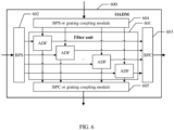
- FIG. 6 is a schematic diagram of a structure of a third OADM and a fourth OADM according to an embodiment of this application.
- a third OADM architecture is an OADM architecture in which a parallel structure is used at both an input-output port and an add-drop port. Specifically, both the add-drop port and the input-output port in the OADM are designed in parallel by using a band pass combiner/splitter.
- a parallel design is used at the input-output port
- a serial design is used at the add-drop port.
- the input-output port of the OADM includes the band pass combiner/splitter
- the add-drop port of the OADM includes a grating coupler and a directional waveguide coupler.
- the OADM 600 shown in FIG. 6 includes a filter unit 601, a BPS 602, a BPC 603, a BPS 604, and a BPC 605.
- a connection relationship between each component is shown in FIG. 6 .
- the filter unit 601 includes a plurality of ADFs.
- the OADM 600 shown in FIG. 6 includes the filter unit 601, the BPS 602, the BPC 603, a grating coupling module 604, and a grating coupling module 605. Structures of the grating coupling module 604 and the grating coupling module 605 are similar to those of the first grating coupling module in FIG. 1 . Details are not described herein again.
- the BPS 602 is configured to split an optical signal at an input port of the OADM 600, and output the split optical signal to each ADF in the filter unit 601.
- the BPS 604 or the grating coupling module 604 is configured to perform a same operation as the BPS 602 on an optical signal of an add port of the OADM 600.
- the BPC 603 is configured to combine the optical signals at output ports of the ADFs in the filter unit 601, and output the combined optical signals to the output port of the OADM 600.
- the BPC 605 or the grating coupling module 605 is configured to perform a same operation as the BPC 603 on optical signals at drop ports of the ADFs in the filter unit 601.
- the third OADM architecture for a connection relationship between the add-drop ports, refer to the related description of the parallel solution used at the add-drop port in FIG. 1 . Details are not described herein again.
- the fourth OADM architecture for a connection relationship between the add-drop ports, refer to related descriptions of the serial solution used at the add-drop port in FIG. 1 . Details are not described herein again.
- the foregoing single-channel or multi-channel parallel solution design may be used at the input-output port.
- a quantity of ADFs in the filter unit 601 is equal to a quantity N of bands.
- a quantity of ADFs in the filter unit 601 is equal to A times the quantity N of bands.
- FIG. 7(a) is a schematic diagram of a structure of a single-channel TOADM apparatus in a third OADM architecture according to an embodiment of this application.
- the TOADM shown in FIG. 7(a) includes cascaded MZIs 701 to 703, a directional coupling module 704, and ADFs 705 to 708.
- the ADFs 705 to 708 are denoted as ADF 1 to ADF 4 respectively.
- the cascaded MZI 701 to 702 use the same design.
- the directional coupling module 704 includes four wavelength-insensitive waveguide directional couplers.
- Wavelength insensitivity means that coupling strength of a waveguide directional coupler is independent of a wavelength.
- connection structure corresponding to each ADF of the TOADM in FIG. 7(a) may be considered as one group of add-drop sub-optical paths, and four groups of sub-optical paths form one add-drop channel or one add-drop port of an optical add-drop multiplexer.
- a to-be-dropped signal ⁇ i is input at an input port of the TOADM, and the cascaded MZI 701 transmits the signal to a corresponding port in I1 to 14 based on different wavelength bands of the signal. It is assumed that ⁇ i is transmitted to 12, the ADF 2 is configured to be in an ON state and drop a wavelength signal ⁇ i , and the wavelength signal ⁇ i is output to a drop port of the TOADM through the waveguide directional coupler at d2.
- a signal ⁇ j is input at the input port of the TOADM, and it is assumed that a wavelength band of the signal ⁇ j corresponds to the port 13, and the wavelength signal ⁇ j needs to pass through the current TOADM, and then go to a next station.
- the ADF 3 is configured to be in an OFF state, and ⁇ j is directly transmitted to t3 by using an input-output waveguide.
- a design of the cascaded MZI 702 is the same as that of the cascaded MZI 701. Only input ports and output ports are exchanged. Therefore, the cascaded MZI 702 and the cascaded MZI 701 have a same band division feature.
- a waveband range corresponding to a port t3 is the same as that of the port I3. Therefore, when ⁇ j is input from t3 to the cascaded MZI 702, ⁇ j is converged to a port O of the TOADM for output.
- a to-be-added signal ⁇ ' i is input at an add port of the TOADM.
- a design of the cascaded MZI 703 is the same as that of the cascaded MZI 701.
- ⁇ ' i is transmitted to a port a2 connected to the ADF 2, and is added to a waveguide 12-12 and transmitted to the port t2 through the ADF 2 that is in the ON state.
- ⁇ ' i is finally output by the cascaded MZI 702 to an output port of the TOADM.
- the ADFs 1 to 4, the cascaded MZI 703, and the four waveguide directional couplers form one group of add-drop ports that are jointly configured to add and/or drop a wavelength ⁇ x in a working range of the TOADM.
- a wavelength ⁇ x in a working range of the TOADM.
- the other three ADFs are all in the OFF state. The ON/OFF state of the ADF and the resonance wavelength of the ADF in the ON state are changed to add/drop signals of different wavelengths.
- the cascaded MZI in FIG. 7(a) may also be replaced by another band pass device having a similar function. This is not limited herein.
- a structure of the cascaded MZIs 701 to 703 refer to the cascaded structures of the MZI in FIG. 8 . Details are not described herein again.
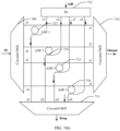
- FIG. 7(b) is another schematic diagram of a structure of a single-channel TOADM apparatus in a third OADM architecture according to an embodiment of this application.
- the TOADM shown in FIG. 7(b) includes cascaded MZIs 709 to 711, 1x4 PS 712, and ADFs 713 to 716.
- the ADFs 713 to 716 are denoted as ADFs 1 to 4.
- the ADFs 1 to 4 may be microring filters with two TCs.
- a main difference of the TOADM in FIG. 7(b) lies in that cascaded MZIs with a same design are used as the band pass combiners/splitters at the input port, the output port, and the drop port, and a wavelength-insensitive power splitter (PS) is used at the add port.
- the PS includes but is not limited to a cascaded star splitter (SS) and a Y-branch splitter (YB).
- SS cascaded star splitter
- YB Y-branch splitter
- a pass-through process of the TOADM in FIG. 7(b) is the same as that in FIG. 7(a) . Details are not described herein again.
- Working principles of add and drop processes of the TOADM in FIG. 7 (b) are as follows:
- the ADFs 1 to 4, the 1x4 PS 712, and the cascaded MZIs 711 form one group of add/drop ports that are jointly configured to add/drop the wavelength ⁇ x .
- the other three ADFs are all in the OFF state. The ON/OFF state of the ADF and the resonance wavelength of the ADF in the ON state are changed to switch add/drop wavelengths.
- FIG. 7(c) is a schematic diagram of a structure of a two-channel TOADM in a third OADM architecture according to an embodiment of this application.
- the TOADM shown in FIG. 7(c) includes a BPS 717, a BPS 719, a BPS 721, a BPC 718, a BPC 720, a BPC 722, and ADFs 723 to 730.
- the BPS 717 and the BPC 718 are separately located at an input port and an output port of the TOADM.
- the BPS 719 and the BPC 720 form one add-drop port of the TOADM.
- the BPS 721 and the BPC 722 form the other add-drop port of TOADM.
- FIG. 7(c) Compared with FIG. 7(a) and FIG. 7(b) , a main difference in FIG. 7(c) lies in that after being connected in series with each other, microring add/drop filters corresponding to sub-optical paths corresponding to each add-drop channel are separately connected to band pass combiners/splitters at an input port and an output port.
- an output port of the BPS 717 is connected to an input port of the ADF 723
- an output port of the ADF 723 is connected to an input port of the ADF 724
- an output port of the ADF 724 is connected to an input port of the BPC 718.
- the add-drop channel formed by the BPS 719 and the BPC 720 in FIG. 7(c) may use the structure of the add-drop channel shown in FIG. 7(a) or FIG. 7(b) .
- the add-drop channel formed by the BPS 721 and the BPC 722 may also be the structure of the add-drop channel shown in FIG. 7(a) or FIG. 7(b) .
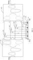
- FIG. 8 is a schematic diagram of a structure of a TOADM apparatus in a fourth OADM architecture according to an embodiment of this application.
- the TOADM shown in FIG. 8 includes cascaded MZIs 801 and 802, a second grating coupling module 803, and ADFs 804 to 807. Both the cascaded MZI 801 and the cascaded MZI 802 are obtained by cascading four MZIs. Dashed lines in FIG. 8 shows one MZI. It can be learned from FIG. 8 that there are MZIs with varied length differences between an upper arm and a lower arm in the four MZIs.
- FIG. 8 is a structure of an input-output port in an integrated serial solution, and is obtained by using a structure of an add-drop port in a parallel solution.
- FIG. 8 is a structure of an add-drop port in the integrated serial solution, and is obtained by using a structure of an input-output in the parallel solution. Therefore, for an input-output port formed by the cascaded MZI 801 and the cascaded MZI 802 in FIG. 8 , refer to related descriptions in FIG. 1 , FIG. 6 , FIG. 7(a) , FIG. 7(b) , and FIG. 7(c) .
- For an add-drop port formed by the second grating coupling module 803 refer to descriptions of the parallel solution in FIG. 1 , FIG. 2 , FIG. 3(a) , FIG. 4 , and FIG. 5 . Details are not described herein again.
- FIG. 9 is a schematic flowchart of an OADM control method according to an embodiment of this application. As shown in FIG. 9 , the OADM control method in this embodiment of this application includes the following steps.
- An OADM inputs, based on wavelength of one or more input optical signals, the one or more input optical signals into a microring filter corresponding to a band to which the one or more input optical signals belong.
- One band corresponds to one or more microring filters, where "more" means two or more, and each microring filter has a different resonance wavelength.
- the one or more input optical signals may include an optical signal input from an input port.
- the one or more input optical signals may include an optical signal input from an add port.
- the one or more input optical signals may include an optical signal input from both the input port and the add port.
- the microring filter may be a microring add/drop filter with a tunable coupler.
- This type of microring add/drop filter may adjust a state (a working state and an offline state) of the microring add/drop filter by using the tunable coupler, to flexibly control the microring add/drop filter.
- a working band range of the microring add/drop filter may be changed by switching between the working state and the offline state.
- the OADM couples a target optical signal from the input port to a drop port, and/or couples the target optical signal from the add port to an output port.
- the target optical signal is an optical signal whose wavelength is equal to a resonance wavelength of the microring filter in the input optical signal.
- the OADM filters and obtains the target optical signal whose wavelength is equal to the resonance wavelength of the microring filter from the optical signal input at the add port, and transmits the target optical signal to the output port, to transmit the target optical signal to a next station.
- a next OADM For example, a next OADM.
- the OADM filters and obtains the target optical signal whose wavelength is equal to the resonance wavelength of the microring filter from the optical signal input at the input port, and transmits the target optical signal to the drop port, and the to-be-dropped optical signal output by the foregoing station (for example, an optical signal receiver) is dropped.
- the add process and the drop process may be performed separately or simultaneously. This is not limited in this application.
- the foregoing add process and/or drop process may be specifically implemented by using the tunable coupler to control the microring add/drop filter to be in the working state.
- the OADM outputs the target optical signal coupled to the output port and/or the drop port.
- the OADM In the add process, the OADM outputs the target optical signal input from the add port, namely, a to-be-added optical signal, to the output port.
- the target optical signal input by the OADM from the input port namely, a to-be-dropped signal, is output to the drop port.
- the OADM adjusts a resonance wavelength of a first microring filter to be equal to a resonance wavelength of a second microring filter.
- the OADM adjusts a working band of a second coupler corresponding to the first microring filter to a band corresponding to the first microring filter to a band corresponding to the second microring filter, to back up a target optical signal corresponding to the second microring filter by using the first microring filter.
- Both the first microring filter and the second microring filter may be one or more filters in a filter unit.
- the microring filter is the microring add/drop filter with the tunable coupler.
- the OADM controls the microring add/drop filter to be in the offline state by using the tunable coupler, couples the input optical signal from the input port to the output port, or couples the input optical signal from the add port to the drop port.
- the OADM outputs the input optical signal coupled to the output and/or the drop port.
- the OADM may further switch between different wavelengths in a band corresponding to a same microring filter.
- the microring filter is the microring add/drop filter with the tunable coupler.
- the OADM controls the microring filter to be in the offline state, adjusts a resonance wavelength of the microring filter from a first wavelength to a second wavelength, and controls the microring filter to be in the working state after the adjustment is completed. Both the first wavelength and the second wavelength belong to the band corresponding to the microring filter.
- the OADM may further switch between wavelengths in bands corresponding to different microring filters.
- the microring filter is the microring add/drop filter with the tunable coupler.
- the OADM controls a third microring filter to be in the offline state, where a resonance wavelength of the third microring filter is the first wavelength.
- the OADM controls a fourth microring filter to be in the offline state, and configures a resonance wavelength of the fourth microring filter as the second wavelength.
- the OADM keeps the third microring filter in the offline state, and switches the fourth microring filter to the working state.
- the offline state or the working state of the microring add/drop filter with the tunable coupler may be controlled by using an electro-optic effect or a thermo-optic effect. This is not limited in this application.
- the OADM may be a three-port apparatus having only a drop function, or a three-port apparatus having only an add function, or a four-port apparatus having both the add function and the drop function.
- OADM control method in this embodiment of this application is consistent with those of the optical add/drop multiplexer in FIG. 1 to FIG. 8 .
- the OADM control method in this embodiment of this application is applicable to all modules and components in FIG. 1 to FIG. 8 , to implement functions of all the modules and components. Details are not described herein again.
- An embodiment not according to the claimed invention further provides an integrated optical chip.
- the OADM described in any one of the embodiments in FIG. 1 to FIG. 8 is integrated into the integrated optical chip.
- the integrated optical chip may be integrated into a system-on-a-chip SoC.
Landscapes
- Physics & Mathematics (AREA)
- Engineering & Computer Science (AREA)
- General Physics & Mathematics (AREA)
- Optics & Photonics (AREA)
- Computer Networks & Wireless Communication (AREA)
- Signal Processing (AREA)
- Microelectronics & Electronic Packaging (AREA)
- Optical Communication System (AREA)
- Optical Modulation, Optical Deflection, Nonlinear Optics, Optical Demodulation, Optical Logic Elements (AREA)
- Optical Integrated Circuits (AREA)
Description
- This application relates to the field of integrated photonic technologies, and in particular, to an optical add/drop multiplexer apparatus and a control method thereof.
- With development of the integrated photonic technology, a microring resonator (MRR) structure starts to be used to build an optical add/drop multiplexer (OADM). Specifically, because there is a linear relationship between a resonance wavelength of an MRR and an effective refractive index of a microring waveguide, the effective refractive index of the microring waveguide in the MRR is changed by using a thermo-optic effect or an electro-optic effect, to change the resonance wavelength of the microring waveguide. In this way, a tunable optical add/drop multiplexer (TOADM) is implemented.
- When the TOADM is used on a wavelength division multiplexing (WDM) network, a tunable range of the resonance wavelength of the MRR is required to reach about 40 nm, to cover a full C band. Currently, a commonly used TOADM uses one or more cascaded microrings with a same waveguide size and radius to form a microring add/drop carrier filter, and the effective refractive index of the microring waveguide is changed by using a phase shifter (PS) based on the thermo-optic effect, to cover the full C band.
- The tunable range of the MRR is determined by a free spectral range (FSR), and the FSR is inversely proportional to a microring radius. In other words, a smaller microring radius indicates a larger FSR. Therefore, for a TOADM that covers the full C band, a microring radius of the TOADM should be small enough to obtain an FSR that covers the full C band. Such a microring radius size imposes an extremely high requirement on stability and reliability of a microring manufacturing process, increasing difficulty in microring manufacturing.
-
EP 2095553 describes a method and device for hitless tunable optical filtering. -
US 2012/257130 describes a tunable wavelength filter based on a symmetric PLC circuit comprising an MZ filter-based demultiplexer, a waveguide resonator, and an MZ filter-based multiplexer. -
CN 101552648 describes a reconfigurable optical add-drop multiplexer (an ROADM structure) for realizing 16 channels with multiple orders. - To address the foregoing technical defects, embodiments of this application provide an optical add/drop multiplexer apparatus and a control method thereof, to reduce a requirement on an FSR of a microring filter by using a band division manner, reduce a radius of the microring filter, reduce manufacturing difficulty of the microring filter, and improve reliability of the optical add/drop multiplexer apparatus.
- According to a first aspect, an embodiment of this application provides an optical add/drop multiplexer apparatus. The optical add/drop multiplexer apparatus is an integrated optical chip, and includes a filter unit, a waveband multiplexer/demultiplexer unit, an input port, an output port, and an add port and/or a drop port. The filter unit includes a plurality of microring filters, the filter unit is connected to the waveband multiplexer/demultiplexer unit, and the waveband multiplexer/demultiplexer unit is separately connected to the input port, the output port, the add port (if present), and the drop port (if present). The waveband multiplexer/demultiplexer unit is configured to input, based on wavelength of one or more input optical signals, the one or more input optical signals into a microring filter corresponding to a band to which the one or more input optical signals belong. One band corresponds to at least one microring filter, and each microring filter has a different resonance wavelength. The one or more input optical signals include an optical signal at the input port and/or an optical signal at the add port (if present). For example, the one or more input optical signals may be the optical signal at the input port, or may be the optical signal at the add port (if present), or may include both the optical signal at the input port and the optical signal at the add port (if present). The filter unit is configured to couple a target optical signal from the input port to the drop port (if present), and/or couple the target optical signal from the add port (if present) to the output port. The target optical signal refers to an optical signal whose wavelength is equal to a resonance wavelength of the microring filter in the input optical signal. The waveband multiplexer/demultiplexer unit is further configured to output the target optical signal coupled to the output port and/or the drop port (if present).
- In the first aspect, different bands are divided, and microring filters corresponding to different bands in the filter unit are used to filter the optical signal. It is easy to understand that after the bands are divided, a wavelength range corresponding to each band may be reduced. In this case, when an optical signal of each band is filtered by using the respective microring filter, a requirement on an FSR of the microring filter may be reduced, and a microring filter with a relatively large microring radius may be used. This reduces manufacturing difficulty of the microring filter, and improves reliability of the optical add/drop multiplexer apparatus.
- It should be noted that, according to the first aspect, an optical add/drop multiplexer apparatus in three solutions are provided: Only the add port is included, only the drop port is included, or the add port and the drop port are included. For ease of subsequent description, a connection structure between the input port and the output port in the optical add/drop multiplexer apparatus is referred to as an input-output port or an input-output channel. Similarly, a connection structure between the add port and the drop port is referred to as an add-drop port or an add-drop channel.
- In a possible implementation of the first aspect, the microring filter has a tunable coupler (TC), and the filter unit is specifically configured to control the microring filter to be in a working state by using the TC, and couple the target optical signal from the input port to the drop port (if present), and/or couple the target optical signal from the add port (if present) to the output port. In this implementation, a status (the working state and an offline state) of a microring add/drop filter may be adjusted by using the tunable coupler, to flexibly control the microring add/drop filter. In addition, a working band range of the microring add/drop filter may be changed by switching between the working state and the offline state.
- In a possible implementation of the first aspect, add-drop ports of the optical add/drop multiplexer apparatus may be connected by using a grating coupler and a directional waveguide coupler. Specifically, the waveband multiplexer/demultiplexer unit may include a first grating coupling module, and the first grating coupling module may include the grating coupler and the waveguide directional coupler. A quantity of grating couplers is equal to a quantity of waveguide directional couplers, and is equal to Y, in other words, Y is equal to (A*N), where A is an integer not less than 1, N indicates a quantity of bands, and N is an integer greater than 2. In other words, the quantity of grating couplers and the quantity of waveguide directional couplers are equal to an integer multiple of the quantity N of bands. When A is 1, the first grating coupling module may include N grating couplers and N waveguide directional couplers. Alternatively, when A is greater than 1, the first grating coupling module may include (A*N) grating couplers and (A*N) waveguide directional couplers. A connection relationship between the grating coupler and the waveguide directional coupler in the first grating coupling module is: A drop port of each grating coupler in the first grating coupling module is separately connected to an add port of a corresponding microring filter, and an add port of each waveguide directional coupler in the first grating coupling module is separately connected to a drop port of the corresponding microring filter. An input port of the first grating coupler is the add port, an output port of an Xth grating coupler is connected to an input port of an Xth waveguide directional coupler, an output port of the Xth waveguide directional coupler is connected to an input port of an (X+1)th grating coupler, and an output port of a Yth waveguide directional coupler is the drop port, where X is a positive integer less than Y In this possible implementation, bands are divided for a to-be-added signal at the add port and a to-be-dropped signal at the drop port by using the grating coupler and the waveguide directional coupler. The wavelength range corresponding to each band is reduced after the bands are divided, and therefore the microring filter filters an optical signal with a relatively small wavelength range, to reduce the requirement on the FSR of the microring filter.
- In a first possible implementation of the first aspect, the add-drop ports of the optical add/drop multiplexer apparatus may alternatively be connected by using the band pass combiner/splitter. Specifically, the waveband multiplexer/demultiplexer unit may include a first band pass combiner/splitter and a second band pass combiner/splitter. A quantity of first band pass combiners/splitters is equal to a quantity of second band pass combiners/splitters, and both are equal to A. Each first band pass combiner/splitter includes one input port and N output ports, and each second band pass combiner/splitter includes N input ports and one output port. The one input port of the first band pass combiner/splitter is one add port, and one output port of the first band pass combiner/splitter is connected to an add port of one microring filter. In other words, the N output ports of the first band pass combiner/splitter are separately connected to add ports of N microring filters. The one output port of the second band pass combiner/splitter is one drop port, and one input port of the second band pass combiner/splitter is correspondingly connected to a drop port of the one microring filter. In other words, the N input ports of the second band pass combiner/splitter are separately connected to drop ports of the N microring filters. A microring filter connected to the input port of the first band pass combiner/splitter and the output port of the second band pass combiner/splitter may be a same microring filter, or may be different microring filters. In this possible implementation, the bands are divided for the to-be-added signal at the add port and the to-be-downloaded signal at the drop port by using a band pass combiner/splitter. After the bands are divided, the wavelength range corresponding to each band is reduced, and therefore the microring filter filters the optical signal with the relatively small wavelength range, to reduce the requirement on the FSR of the microring filter.
- The add-drop ports of the optical add/drop multiplexer apparatus are connected by using the grating coupler and the directional waveguide coupler. In other words, the waveband multiplexer/demultiplexer unit includes the first grating coupling module. Alternatively, the add-drop ports of the optical add/drop multiplexer apparatus are connected by using the band pass combiner/splitter. In other words, the waveband multiplexer/demultiplexer unit includes the band pass combiner/splitter. Correspondingly, input-output ports of the optical add/drop multiplexer apparatus may be connected by using the grating coupler.
- In a possible implementation of the first aspect, one add-drop channel is used as an example to describe the connection structure of the input-output port of the optical add/drop multiplexer apparatus by using the grating coupler. Specifically, the waveband multiplexer/demultiplexer unit includes the first grating coupling module. Alternatively, in addition to the first band pass combiner/splitter and the second band pass combiner/splitter, the waveband multiplexer/demultiplexer unit may include a second grating coupling module. The second grating coupling module includes a grating coupler, and a quantity of grating couplers in the second grating coupling module is equal to the quantity N of bands, where N is an integer not less than 2. In a case in which there is only one add-drop channel, A is equal to 1, and one band corresponds to one microring filter. The filter unit includes the N microring filters, and one grating coupler in the second grating coupling module corresponds to one microring filter. A connection relationship between the microring filter and the grating coupler is: In the second grating coupling module, a drop port of each grating coupler is separately connected to an input port of a corresponding microring filter, and an add port of each grating coupler is separately connected to an output port of the corresponding microring filter. An input port of a first grating coupler is the input port, an output port of an Mth grating coupler is coupled to an input port of an (M+1)th grating coupler, and an output port of an Nth grating coupler is the output port, where M is an integer not greater than N.
- In a possible implementation of the first aspect, a plurality of add-drop channels are used as an example to describe the connection structure of the input-output port of the optical add/drop multiplexer apparatus by using the grating coupler. Specifically, the waveband multiplexer/demultiplexer unit includes the first grating coupling module. Alternatively, in addition to the first band pass combiner/splitter and the second band pass combiner/splitter, the waveband multiplexer/demultiplexer unit may include a second grating coupling module. The second grating coupling module includes a grating coupler, and a quantity of grating couplers in the second grating coupling module is equal to the quantity N of bands, where N is an integer not less than 2. In a case in which there are the plurality of add-drop channels, A is an integer greater than 1, A is a quantity of add-drop channels, and one band corresponds to the plurality of microring filters. The filter unit includes (A*N) microring filters, and one grating coupler in the second grating coupling module corresponds to A microring filters. In the second grating coupling module, a drop port of each grating coupler is separately connected to an input port of a first microring filter in the A corresponding microring filters, and an add port of each grating coupler is separately connected to an output port of an Ath microring filter in the A corresponding microring filters. An input port of a first grating coupler is the input port, an output port of an Mth grating coupler is coupled to an input port of an (M+1)th grating coupler, and an output port of an Nth grating coupler is the output port, where M is an integer not greater than N. In the A microring filters corresponding to each grating coupler, an output port of an Xth microring filter is connected to an input port of an (X+1)th microring filter, where X is an integer not less than 1.
- In any one of the foregoing designs of the add-drop port, the input-output ports of the optical add/drop multiplexer apparatus may be connected by using the band pass combiner/splitter.
- In a possible implementation of the first aspect, one add-drop channel is used as an example to describe a connection structure of a band pass combiner/splitter that may be used between input-output ports of the optical add/drop multiplexer apparatus. Specifically, the waveband multiplexer/demultiplexer unit includes the first grating coupling module. Alternatively, in addition to the first band pass combiner/splitter and the second band pass combiner/splitter, the waveband multiplexer/demultiplexer unit may further include a third band pass combiner/splitter and a fourth band pass combiner/splitter. The third band pass combiner/splitter includes one input port and N output ports, and the fourth band pass combiner/splitter includes N input ports and one output port. When there is only one add-drop channel, A is equal to 1, and one band corresponds to one microring filter. The filter unit includes the N microring filters, and the input port of the third band pass combiner/splitter is the input port. The N output ports of the third band pass combiner/splitter are separately connected to input ports of the N microring filters, output ports of the N microring filters are separately connected to the N input ports of the fourth band pass combiner/splitter, and the output port of the fourth band pass combiner/splitter is the output port.
- In a possible implementation of the first aspect, a plurality of add-drop channels are used as an example to describe a connection structure of a band pass combiner/splitter that may be used between input-output ports of the optical add/drop multiplexer apparatus. Specifically, the waveband multiplexer/demultiplexer unit includes the first grating coupling module. Alternatively, the waveband multiplexer/demultiplexer unit including the first band pass combiner/splitter and the second band pass combiner/splitter may further include a third band pass combiner/splitter and a fourth band pass combiner/splitter. The third band pass combiner/splitter includes one input port and N output ports, and the fourth band pass combiner/splitter includes N input ports and one output port. When there are the plurality of add-drop channels, A is an integer greater than 2, A is a quantity of add-drop channels, and one band corresponds to the plurality of microring filters. The filter unit includes (A*N) microring filters, and the input port of the third band pass combiner/splitter is the input port. One output port of the third band pass combiner/splitter and one input port of the fourth band pass combiner/splitter correspond to A same microring filters. Each output port of the third band pass combiner/splitter is connected to an input port of a first microring filter in the A corresponding microring filters, each input port of the fourth band pass combiner/splitter is connected to an output port of an Ath microring filter in the A corresponding microring filters, and the output port of the fourth band pass combiner/splitter is the output port. In the corresponding A microring filters, an output port of an Xth microring filter is connected to an input port of an (X+1)th microring filter, where X is an integer not less than 1.
- In a possible implementation of the first aspect, the filter unit is further configured to adjust a resonance wavelength of the first microring filter to be equal to a resonance wavelength of a second microring filter. The waveband multiplexer/demultiplexer unit is further configured to adjust a working band of a waveguide directional coupler corresponding to the first microring filter from a band corresponding to the first microring filter to a band corresponding to the second microring filter, to back up a target optical signal corresponding to the second microring filter by using the first microring filter. Both the first microring filter and the second microring filter may be one or more filters in the filter unit. In the foregoing technical solution, the working band range of the waveguide directional coupler may be changed, so that sub-optical paths corresponding to the microring filters serve as mutual backup. If a microring add/drop filter in one group of optical paths fails, a wavelength signal may be transmitted through a backup sub-optical path by changing the working band range of the directional coupler. Finally, a wavelength add/drop function is implemented by using a microring filter with a tunable resonance wavelength.
- In a possible implementation of the first aspect, either of the add port and/or the drop port is connected to a wedge-shaped waveguide, or is connected to an anti-reflection waveguide or a blocking waveguide that is based on an absorbing material. Alternatively, a waveguide corresponding to one of the add port and the drop port of the microring filter is a wedge-shaped waveguide, or an anti-reflection waveguide or a blocking waveguide that is based on an absorbing material. It should be noted that the add port or the drop port may alternatively be suspended (not connected to any waveguide). The foregoing technical solution may allow the add port or the drop port to have a high-loss structure having an anti-reflection function, and therefore a corresponding optical signal add/drop function cannot be implemented. It may be considered that the add port or the drop port exists but is unavailable, or it may be considered that the add port or the drop port does not exist.
- In a possible implementation of the first aspect, the grating coupler includes but is not limited to a grating-assisted directional coupler and/or a grating-assisted contra-directional coupler. Specifically, all grating couplers in the first grating coupling module may be grating-assisted directional couplers. Alternatively, all the grating couplers in the first grating coupling module may be grating-assisted contra-directional couplers. Alternatively, there may be several grating-assisted directional couplers and several grating-assisted contra-directional couplers.
- In a possible implementation of the first aspect, the band pass splitter includes but is not limited to a cascaded Mach-Zehnder interferometer and/or a wavelength-insensitive directional coupling element. The wavelength-insensitive directional coupling element includes but is not limited to a wavelength-insensitive power splitter (PS) and a wavelength-insensitive waveguide directional coupler. In addition, the PS may include a cascaded star splitter (SS) and a Y-branch splitter (Y-branch).
- In a possible implementation of the first aspect, the microring filter may include but is not limited to a microring add/drop filter with a TC.
- According to a second aspect, an embodiment of this application provides a control method for an optical add/drop multiplexer apparatus, including: inputting, based on wavelength of one or more input optical signals, the one or more input optical signals into a microring filter corresponding to a band to which the one or more input optical signals belong, where one band corresponds to at least one microring filter, each microring filter has a different resonance wavelength, and the one or more input optical signals include an optical signal at an input port and/or an add port; coupling a target optical signal from the input port to a drop port, and/or coupling a target optical signal from the add port to an output port, where the target optical signal is an optical signal whose wavelength is equal to a resonance wavelength of the microring filter in the input optical signal; and outputting the target optical signal coupled to the output port and/or the drop port.
- In a possible implementation of the second aspect, the microring filter has a TC, and the method specifically includes: controlling, by using the TC, the microring filter to be in a working state, and coupling the target optical signal from the input port to the drop port, and/or coupling the target optical signal from the add port to the
- In a possible implementation of the second aspect, the control method for the optical add/drop multiplexer apparatus further includes: adjusting a resonance wavelength of a first microring filter to be equal to a resonance wavelength of a second microring filter; and adjusting a working band of a second coupler corresponding to the first microring filter from a band corresponding to the first microring filter to a band corresponding to the second microring filter, to back up a target optical signal corresponding to the second microring filter by using the first microring filter. Both the first microring filter and the second microring filter may be one or more filters in a filter unit.
- In a possible implementation of the second aspect, the control method for the optical add/drop multiplexer apparatus further includes: controlling, by using the TC, the microring filter to be in an offline state, and coupling the one or more input optical signals from the input port to the output port, or coupling the one or more input optical signals from the add port to the drop port; and outputting the one or more input optical signals coupled to the output port and/or the drop port.
- In a possible implementation of the second aspect, the optical add/drop multiplexer apparatus may further switch between different wavelengths in a band corresponding to a same microring filter. Specifically, the control method for the optical add/drop multiplexer apparatus further includes: controlling the microring filter to be in the offline state, adjusting a resonance wavelength of the microring filter from a first wavelength to a second wavelength, and controlling the microring filter to be in the working state after the adjustment is completed, where both the first wavelength and the second wavelength belong to the band corresponding to the microring filter.
- In a possible implementation of the second aspect, the optical add/drop multiplexer apparatus may further switch between wavelengths in bands corresponding to different microring filters. Specifically, the control method of the optical add/drop multiplexer apparatus further includes: controlling a third microring filter to be in the offline state, where a resonance wavelength of the third microring filter is the first wavelength; controlling a fourth microring filter to be in the offline state, and configuring a resonance wavelength of the fourth microring filter as the second wavelength; and keeping the third microring filter in the offline state, and switching the fourth microring filter to the working state.
- It should be noted that, for other descriptions and beneficial effects corresponding to the second aspect and the possible implementations of the second aspect, refer to related descriptions in the first aspect and the related implementations of the first aspect. Details are not described herein again.
- According to a third aspect, an embodiment not according to the claimed invention further provides an integrated optical chip, and the optical add/drop multiplexer apparatus according to any one of the first aspect or the implementations of the first aspect is integrated into the integrated optical chip. In a design, the integrated optical chip may be integrated into a system-on-a-chip SoC.
-
-
FIG. 1 is a schematic diagram of a structure of an OADM according to an embodiment of this application; -
FIG. 2 is a schematic diagram of a structure of a first OADM and a second OADM according to an embodiment of this application; -
FIG. 3(a) is a schematic diagram of a structure of a single-channel TOADM apparatus in a first OADM architecture according to an embodiment of this application; -
FIG. 3(b) is a schematic connection diagram of a GADC, an ADF, and a waveguide directional coupler according to an embodiment of this application; -
FIG. 4 is a schematic diagram of a structure of a single-channel TOADM apparatus in a second OADM architecture according to an embodiment of this application; -
FIG. 5 is a schematic diagram of a structure of a two-channel TOADM apparatus in a first OADM architecture according to an embodiment of this application; -
FIG. 6 is a schematic diagram of a structure of a third OADM and a fourth OADM according to an embodiment of this application; -
FIG. 7(a) is a schematic diagram of a structure of a single-channel TOADM apparatus in a third OADM architecture according to an embodiment of this application; -
FIG. 7(b) is another schematic diagram of a structure of a single-channel TOADM apparatus in a third OADM architecture according to an embodiment of this application; -
FIG. 7(c) is a schematic diagram of a structure of a two-channel TOADM in a third OADM architecture according to an embodiment of this application; -
FIG. 8 is a schematic diagram of a structure of a TOADM apparatus in a fourth OADM architecture according to an embodiment of this application; and -
FIG. 9 is a schematic flowchart of an OADM control method according to an embodiment of this application. - Embodiments of this application provide an optical add/drop multiplexer apparatus and a control method thereof, to reduce a microring radius by using a band division manner, reduce manufacturing difficulty of a microring filter, and improve reliability of the optical add/drop multiplexer apparatus.
- In the specification, claims, and the accompanying drawings of this application, the terms "first", "second", and the like are intended to distinguish between similar objects but do not necessarily indicate a specific order or sequence. It should be understood that the terms used in such a way are interchangeable in proper circumstances, and this is merely a distinguishing manner for describing objects having a same attribute in the embodiments of this application. In addition, the terms "include", "have" and any other variants mean to cover the non-exclusive inclusion, so that a process, method, system, product, or device that includes a series of units is not necessarily limited to those units, but may include other units not expressly listed or inherent to such a process, method, system, product, or device. "Waveband" and "band" in following descriptions have a same meaning, and "and/or" means that at least one of the items is included. For example, "A and/or B" may be A, may be B, or may be A and B. The "working state" in the embodiments of this application may be referred to as an "online state" or an "on state". Similarly, the "non-working state" may be referred to as an "offline state" or an "off state".
- The following describes the embodiments of this application with reference to the accompanying drawings.
-
FIG. 1 is a schematic diagram of a structure of an OADM according to an embodiment of this application. As shown inFIG. 1 , theOADM 100 is an integrated optical chip, and theOADM 100 may include afilter unit 101, a waveband multiplexer/demultiplexer unit 102, aninput port 103, anoutput port 104, anadd port 105, and/or adrop port 106. It should be noted that theOADM 100 may include theadd port 105 or thedrop port 106, namely, to form a three-port OADM. Alternatively, theOADM 100 may also include the add port and the drop port, namely, to form a four-port OADM. Specifically, a design may be performed according to an actual requirement. This is not limited in this application. - The waveband multiplexer/
demultiplexer unit 102 is configured to input, based on wavelength of one or more input optical signals, the one or more input optical signals into a microring filter corresponding to a band to which the one or more input optical signals belong. One band corresponds to at least one microring filter, and each microring filter has a different resonance wavelength. The one or more input optical signals include an optical signal at theinput port 103 and/or theadd port 105. For example, the one or more input optical signals may be an optical signal at theinput port 103, or may be an optical signal at theadd port 105, or may include both the optical signal at theinput port 103 and the optical signal at theadd port 105. - The
filter unit 101 is configured to control the microring filter to be in a working state, and couple the target optical signal from theinput port 103 to thedrop port 106, and/or couple the target optical signal from theadd port 105 to theoutput port 104. The target optical signal is an optical signal whose wavelength is equal to a resonance wavelength of the microring filter in the input optical signal. The waveband multiplexer/demultiplexer unit 102 is further configured to output the target optical signal coupled to theoutput port 104 and/or thedrop port 106. - It should be understood that a connection structure between the input port and the output port in the OADM may be referred to as an input-output port or an input-output channel. Similarly, a connection structure between the add port and the drop port may be referred to as an add-drop port or an add-drop channel. The following describes the
OADM 100 in this embodiment of this application in detail with reference to the input-output channel and the add-drop channel. - The add-drop channel of the
OADM 100 can be designed by using a serial solution or a parallel solution. - When the serial solution is used, the add-drop channel of the
OADM 100 may specifically include a grating coupler and a directional waveguide coupler. To be specific, the waveband multiplexer/demultiplexer unit 102 may include a first grating coupling module. The first grating coupling module may include the grating coupler and the waveguide directional coupler. A quantity of grating couplers is equal to a quantity of waveguide directional couplers and is equal to Y, where Y is equal to (A*N), A is an integer not less than 1, N indicates a quantity of bands, and N is an integer greater than 2. - A connection relationship between the grating coupler, the waveguide directional coupler, and the microring filter in the
OADM 100 is specifically as follows: A drop port of each grating coupler in the first grating coupling module is separately connected to an add port of a corresponding microring filter, and an add port of each waveguide directional coupler in the first grating coupling module is separately connected to a drop port of the corresponding microring filter. An input port of the first grating coupler is theadd port 105, an output port of an Xth grating coupler is connected to an input port of an Xth waveguide directional coupler, an output port of the Xth waveguide directional coupler is connected to an input port of an (X+1)th grating coupler, and an output port of a Yth waveguide directional coupler is thedrop port 106, where X is a positive integer less than Y - It should be noted that A represents a quantity of add-drop channels of the
OADM 100. For example, when A=1, it indicates that there is one add-drop channel, and when A> 1, it indicates that there a plurality of add-drop channels. - When the
OADM 100 is designed with three ports, a wedge-shaped waveguide, or an anti-reflection waveguide or a blocking waveguide that is based on an absorbing material may be disposed at a specific port of the microring filter. For example, for theOADM 100 having only an add function, the waveguide mentioned above may be disposed at a drop port of each microring filter of theOADM 100. Similarly, a design manner of an optical add/drop multiplexer apparatus having only a drop function includes: The wedge-shaped waveguide, or the anti-reflection waveguide or the blocking waveguide that is based on the absorbing material is disposed as a waveguide (namely, an add waveguide) corresponding to an add port of each microring filter in the optical add/drop multiplexer apparatus 100. It should be noted that the foregoing three-port design solution is applicable to OADMs with one or more add-drop channels. It should be noted that the add port or the drop port may alternatively be suspended (not connected to any waveguide). The foregoing technical solution may allow the add port or the drop port to be a high-loss structure having an anti-reflection function, and therefore an optical signal add/drop function cannot be implemented. It may be considered that the add port or the drop port exists but is unavailable, or it may be considered that the add port or the drop port does not exist. - When the parallel solution is used, the add-drop channel of the optical add-
drop multiplexer apparatus 100 may be formed by connecting band pass combiners/splitters. Specifically, the waveband multiplexer/demultiplexer unit 102 may include a first band pass combiner/splitter and a second band pass combiner/splitter. A quantity of first band pass combiners/splitters is equal to a quantity of second band pass combiners/splitters, and both are equal to A. Each first band pass combiner/splitter includes one input port and N output ports, and each second band pass combiner/splitter includes N input ports and one output port. The one input port of the first band pass combiner/splitter is theadd port 105. One output port of the first band pass combiner/splitter is connected to an add port of one microring filter. To be specific, the N output ports of the first band pass combiner/splitter are separately connected to add ports of N microring filters. The one output port of the second band pass combiner/splitter is thedrop port 106. One input port of the second band pass combiner/splitter is correspondingly connected to a drop port of the one microring filter. To be specific, the N input ports of the second band pass combiner/splitter are separately connected to drop ports of the N microring filters. - Either the parallel solution or the serial solution is used to design the add-drop port, the grating coupler may be used to perform serial connection between input-output ports of the OADM. The waveband multiplexer/
demultiplexer unit 102 may further include a second grating coupling module. The second grating coupling module includes a grating coupler. A quantity of grating couplers is equal to the quantity N of the bands. - When A is equal to 1, one band corresponds to one microring filter, and the
filter unit 101 includes the N microring filters. One grating coupler in the second grating coupling module corresponds to one microring filter. A connection relationship between the microring filter and the grating coupler is as follows: A drop port of each grating coupler is separately connected to an input port of a corresponding microring filter. An add port of each grating coupler is separately connected to an output port of the corresponding microring filter. An input port of a first grating coupler is theinput port 103. An output port of an Mth grating coupler is coupled to an input port of an (M+1)th grating coupler. An output port of an Nth grating coupler is theoutput port 104, where M is an integer not greater than N. - When A is greater than 1, in other words, in a multi-channel design, one band corresponds to a plurality of microring filters. The
filter unit 101 includes (A*N) microring filters. One grating coupler in the second grating coupling module corresponds to A microring filters. A drop port of each grating coupler in the second grating coupling module is connected to an input port of a first microring filter in the A corresponding microring filters. An add port of each grating coupler is separately connected to an output port of an Ath microring filter in the A corresponding microring filters. An input port of a first grating coupler is theinput port 103. The output port of the Mth grating coupler is coupled to the input port of the (M+1)th grating coupler. The output port of the Nth grating coupler is theoutput port 104, where M is an integer not greater than N. In the A microring filters corresponding to each grating coupler, an output port of an Xth microring filter is connected to an input port of an (X+1)th microring filter, where X is an integer not less than 1. - Alternatively, the input-output ports of the OADM may be connected in parallel by using the band pass combiner/splitter. The waveband multiplexer/
demultiplexer unit 102 may further include a third band pass combiner/splitter and a fourth band pass combiner/splitter. The third band pass combiner/splitter includes one input port and N output ports, and the fourth band pass combiner/splitter includes N input ports and one output port. - A is equal to 1, and one band corresponds to one microring filter. The
filter unit 101 includes the N microring filters. The input port of the third band pass combiner/splitter is theinput port 103, and the N output ports of the third band pass combiner/splitter are separately connected to input ports of the N microring filters. Output ports of the N microring filters are respectively connected to the N input ports of the fourth band pass combiner/splitter, and the output port of the fourth band pass combiner/splitter is theoutput port 104. - A is an integer greater than 1, namely, A is the quantity of add-drop channels, and one band corresponds to the plurality of microring filters. The
filter unit 101 includes the (A*N) microring filters. The input port of the third band pass combiner/splitter is theinput port 103, and one output port of the third band pass combiner/splitter and one input port of the fourth band pass combiner/splitter correspond to A same microring filters. Each output port of the third band pass combiner/splitter is connected to an input port of a first microring filter in the A microring filters corresponding to the third band pass combiner/splitter. Each input port of the fourth band pass combiner/splitter is connected to an output port of an Ath microring filter in the A microring filters corresponding to the fourth band pass combiner/splitter. The output port of the fourth band pass combiner/splitter is theoutput port 104. In the corresponding A microring filters, an output port of an Xth microring filter is connected to an input port of an (X+1)th microring filter, where X is an integer not less than 1. - In an embodiment, the filter unit is further configured to adjust a resonance wavelength of the first microring filter to be equal to a resonance wavelength of a second microring filter. The waveband multiplexer/demultiplexer unit is further configured to adjust a working band of a waveguide directional coupler corresponding to the first microring filter from a band corresponding to the first microring filter to a band corresponding to the second microring filter, to back up a target optical signal corresponding to the second microring filter by using the first microring filter. Both the first microring filter and the second microring filter may be one or more filters in the filter unit. For example, the filter unit includes eight microring filters (numbered 1 to 8). The first microring filter is an odd-numbered microring filter, and the second microring filter is an even-numbered microring filter.
- The grating coupler includes but is not limited to a grating-assisted directional coupler and/or a grating-assisted contra-directional coupler. Specifically, all the grating couplers in the first grating coupling module may be grating-assisted directional couplers. Alternatively, all the grating couplers in the first grating coupling module may be grating-assisted contra-directional couplers. Alternatively, the two types of couplers are used together.
- The band pass splitter includes but is not limited to a cascaded Mach-Zehnder interferometer and/or a wavelength-insensitive directional coupling element. The wavelength-insensitive directional coupling element includes but is not limited to a wavelength-insensitive power splitter (PS) and a wavelength-insensitive waveguide directional coupler. In addition, the PS may be a cascaded star splitter star splitter and a Y-branch splitter Y-branch.
- Optionally, the microring filter may be a microring add/drop filter (ADF) with a tunable coupler (TC). Compared with a common ADF, the ADF with the TC is different in that the ADF can be controlled to be in a working or an offline state by using the TC. In the working state, the ADF generates a filter effect on an optical signal input into the ADF. Specifically, the ADF filters, to a microring, an optical signal whose wavelength is equal to a resonance wavelength of the microring in the input optical signal, so that the optical signal can be coupled from one waveguide to another waveguide. For example, an input-output waveguide is coupled to an add-drop waveguide, and/or the add-drop waveguide is coupled to the input-output waveguide. In the offline state, the ADF does not filter the optical signal input into the ADF. It should be noted that one port of the input-output waveguide is the
input port 103, and the other port is theoutput port 104. One port of the add-drop waveguide is theadd port 105, and the other port is thedrop port 106. - In this embodiment of this application, different bands are divided, and microring filters corresponding to different bands in the filter unit are used for filtering. It should be understood that band division may reduce a band range corresponding to each band. In this case, when optical signals in respective bands are filtered by using respective microring filters, a requirement on an FSR of the microring filter may be reduced. The OADM may use a microring filter with a relatively large microring radius, to reduce manufacturing difficulty of the microring filter, and improve reliability of the optical add/drop multiplexer apparatus.
- The following describes in detail the OADM apparatus provided in this embodiment of this application from the plurality of OADM design manners mentioned above.
-
FIG. 2 is a schematic diagram of a structure of a first OADM and a second OADM according to an embodiment of this application. - In a first OADM architecture, a serial solution design is used for an input-output port and an add-drop port. Specifically, an add-drop port in an OADM includes a grating coupler and a directional waveguide coupler, and an input-output port of the OADM includes a grating coupler. In a second OADM architecture, the serial solution design is used for the input-output port, and a parallel solution design is used for the add-drop port. Specifically, the add-drop port of the OADM is formed by the grating coupler and the directional waveguide coupler, and the input-output port of the OADM is formed by a band pass combiner/splitter.
- In one aspect, the
OADM 200 in the first OADM architecture includes aninput port 201, anoutput port 202, anadd port 203, adrop port 204, afilter unit 205, agrating coupling module 207, and agrating coupling module 206. Thegrating coupling module 206 includes a plurality of grating couplers. Thegrating coupling module 207 includes a plurality of grating couplers and a waveguide directional coupler. - Correspondingly, the waveband multiplexer/
demultiplexer unit 102 inFIG. 1 may specifically include thegrating coupling module 206 and thegrating coupling module 207 shown inFIG. 2 . A quantity of grating couplers in thegrating coupling module 206 is equal to a quantity of divided bands. Thegrating coupling module 206 is the second grating coupling module in the waveband multiplexer/demultiplexer unit 102 inFIG. 1 . A quantity of grating couplers in thegrating coupling module 207 is equal to a quantity of waveguide directional couplers, and is equal to a quantity of microring filters in thefilter unit 205. Thegrating coupling module 207 is the first grating coupling module in the waveband multiplexer/demultiplexer unit 102 inFIG. 1 . - In another aspect, the
OADM 200 in the second OADM architecture includes theinput port 201, theoutput port 202, theadd port 203, thedrop port 204, thefilter unit 205, thegrating coupling module 206, a band pass combiner/splitter 208, and a band pass combiner/splitter 209. - Compared with the first OADM architecture, the second OADM architecture is different in that: The waveband multiplexer/
demultiplexer unit 102 inFIG. 1 specifically includes thegrating coupling module 206 shown inFIG. 2 , the band pass combiner/splitter 208, and the band pass combiner/splitter 209. A quantity of output ports of the band pass combiner/splitter 208 and a quantity of input ports of the band pass combiner/splitter 209 are both equal to the quantity of divided bands. A quantity of the band pass combiners/splitters 208 and a quantity of the band pass combiners/splitters 209 are both equal to a quantity of add-drop channels. The band pass combiner/splitter 208 is the third band pass combiner/splitter located at the add port of the waveband multiplexer/demultiplexer unit 102 inFIG. 1 . The band pass combiner/splitter 209 is the fourth band pass combiner/splitter located at the drop port of the waveband multiplexer/demultiplexer unit 102 inFIG. 1 . - In the first OADM architecture, for a connection relationship between the
add port 203 and thedrop port 204, refer to related descriptions in the embodiment in which the add port and the drop port use the grating coupler and the directional waveguide coupler inFIG. 1 . Details are not described herein again. Similarly, in the second OADM architecture, for a connection relationship between theadd port 203 and thedrop port 204, refer to related descriptions in the embodiment in which the add port and the drop port use the band pass combiner/splitter. Details are not described herein again. - In the foregoing two architectures, connection manner between the
input port 201 and theoutput port 202 may be specifically the single-channel and multi-channel serial connection manner described inFIG. 1 . In the single-channel serial connection manner, the quantity of microring filters in thefilter unit 205 is equal to the quantity N of bands. In the multi-channel serial connection manner, the quantity of microring filters in thefilter unit 205 is A times the quantity of bands, where A is an integer greater than 1. Single-channel and multi-channel refer to one or more add-drop channels. A change in the quantity of add-drop channels does not lead to a change in a structure of each add-drop channel, but leads to a difference in a connection structure between the add-drop channel and an input-output channel. For details, refer to related descriptions in the embodiments inFIG. 3(a) andFIG. 5 . Details are not described herein again. - Based on the two OADM architectures shown in
FIG. 2 , the following separately describes the first and the second OADM architectures in the embodiments of this application by using a tunable optical add/drop multiplexer (TOADM) as an example. The OADM architectures use an ADF with a tunable coupler TC to divide a C band in a 32 nm wavelength range. -
FIG. 3(a) is a schematic diagram of a structure of a single-channel TOADM apparatus in a first OADM architecture according to an embodiment of this application. As shown inFIG. 3(a) , the TOADM includes grating-assisted directional couplers (GADC) 301 to 304, 313 to 316,ADFs 305 to 308, waveguidedirectional couplers 309 to 312, aninput port 317, anoutput port 318, adrop port 319, and anadd port 320. - The GADC has four ports (Gi, Gd, Go, and Ga). In the GADC, an optical path direction is as follows: A signal is input from Gi, a signal whose signal wavelength is in a GADC band range is transmitted to Gd, and other optical signals are transmitted to Go. A signal is input from the Ga, a signal whose signal wavelength is in the GADC band range is transmitted to Go, and other signals are transmitted to Gd.
- In
FIG. 3(a) , a C band in a 32 nm wavelength range is divided into four sub-bands at a granularity of 0.1 nm. Each sub-band includes optical signals of 20 wavelengths, and the four sub-bands separately correspond to theADFs 305 to 308. - To describe a connection structure of the TOADM in
FIG. 3(a) ,FIG. 3(b) shows connection relationships between theGADC 301, theGADC 313, theADF 305, and the waveguidedirectional coupler 309. A drop port of theGADC 301 is connected to an input port of theADF 305, an add port of theGADC 301 is connected to an output port of theADF 305, an add port of theADF 305 is connected to a drop port of theGADC 313, a drop port of theADF 305 is connected to an add port of theGADC 313, and an output port of theGADC 313 is connected to an input port of the waveguidedirectional coupler 309. Each group of connection structures shown inFIG. 3(b) of the tunable optical add/drop multiplexer TOADM inFIG. 3(a) may be considered as one group of add-drop sub-optical paths, and four groups of sub-optical paths form one add-drop port of the optical add/drop multiplexer. Working principles of drop, add, and pass-through processes of the optical add/drop multiplexer are as follows. - Drop process: A to-be-dropped signal λi entering from the
input port 317 is transmitted along an input-output waveguide. It is assumed that λi is in a wavelength selection range of the grating-assisteddirectional coupler 302, the signal λi directly passes through the grating-assisteddirectional coupler 301, and enters a second group of add-drop sub-optical paths (namely, the ADF 306) through the grating-assisteddirectional coupler 302. TheADF 306 is in a working state, and a resonance wavelength of theADF 306 is configured at λi. The signal λi is dropped by theADF 306 to a port d2, and is transmitted to thedrop port 319 along an add-drop waveguide. A wavelength selection range of theGADC 313 at a1 is the same as that of theGADC 301. The signal λi passes through theGADC 313, and is output at thedrop port 319. Because remaining wavelength signals that are in the wavelength selection range of theGADC 302 do not meet a resonance condition of theGADC 302, and therefore the remaining wavelength signals pass through theADF 306, and are coupled back to the input-output waveguide by theGADC 302 for forward transmission. - Pass-through process: λj enters from the
input port 317. It is assumed that a band range of λj corresponds to the band range of the GADC 303, a wavelength signal of λj needs to pass through the current TOADM, and then go to a next station. The signal λj passes through theGADCs ADF 307 is configured to be in an offline "OFF" state, and the signal λj directly passes through theADF 307. After passing through the GADC 303, the signal returns to the input-output waveguide, directly passes through theGADC 304, and then is output from theoutput port 318. - Add process: A to-be-added signal λ'i enters from the
add port 320. In the four groups of add-drop sub-optical paths, all ai (i = 1, 2, 3, 4) ports use waveguide directional couplers having a same wavelength selection range as the GADC. Therefore, the signal λ'i directly passes through theGADCs GADC 314. The ADF306 is in the working state, and the resonance wavelength of theADF 306 is configured at λi. The signal λ'i is added by theADF 306 and is output by theGADC 302 to the input-output waveguide for transmission toward theoutput port 318. Because λ'i is not in wavelength selection ranges of theGADCs 303 and 304, the signal λ'i directly passes through theGADCs 303 and 304, and is output from theoutput port 318. - The
ADFs 305 to 308, theGADCs 309 to 312, and the waveguidedirectional couplers 313 to 316 together form one add-drop channel of the TOADM, which is used to add/drop a wavelength λx. Only one ADF corresponding to a band in which λx is located is in an ON state, and a resonance wavelength of the ADF is configured at λx. The other three ADFs are all in the OFF state. The ON/OFF state of the ADF and the resonance wavelength of the ADF in the ON state are changed to switch add/drop wavelengths. - It should be noted that the working state or the offline state of the ADF may be controlled by using an electro-optic effect or a thermo-optic effect. It should be further noted that, in
FIG. 3(a) , theGADCs 301 to 304 and theGADCs 313 to 316 are both GADCs. In some embodiments, all or some of theGADCs 301 to 304 and theGADCs 313 to 316 may be replaced with grating-assisted contra-directional couplers (GACDC). Working principles of the two grating couplers are the same. A connection structure of a replaced TOADM is similar to that inFIG. 3(a) . Details are not described herein again. A difference lies in that positions of Ga and Gd of the replaced grating coupler are exchanged, and the direction of the optical path connected to the ports of the TOADM needs to be changed accordingly. - A wavelength selection range of the waveguide directional coupler is determined based on a grating structure. When the waveguide directional coupler works normally, there is no need to perform active switching control. However, if a thin film heater is used to heat a grating region of the waveguide directional coupler, a refraction coefficient of the waveguide directional coupler changes, and a working range of the waveguide directional coupler may be changed. The four groups of add-drop sub-optical paths shown in
FIG. 3(a) in the waveguide directional coupler serve as mutual backup. If an ADF in one group of sub-optical paths fails, the working range of the waveguide directional coupler may be changed, so that the wavelength signal is transmitted through a backup sub-optical path, to implement backup with an ADF with a tunable resonance wavelength. -
FIG. 4 is a schematic diagram of a structure of a single-channel TOADM apparatus in a second OADM architecture according to an embodiment of this application. The TOADM shown inFIG. 4 includesGADCs 401 to 404,ADFs 405 to 408, a band pass combiner (BPC) 409, a band pass splitter (BPS) 410, anoutput port 411, anoutput port 412, anadd port 413, and adrop port 414. - Structures and functions of the grating-assisted
directional couplers 401 to 404 and the microring add/drop filters 405 to 408 in the TOADM shown inFIG. 4 are separately similar to those of the grating-assisteddirectional couplers 301 to 304 and the microring add/drop filters 305 to 308 in the foregoing embodiment inFIG. 3(a) . For related descriptions, refer to related descriptions inFIG. 3(a) . This is not limited herein. - Compared with the single-channel TOADM in the first OADM architecture shown in
FIG. 3(a) , the single-channel TOADM in the second OADM architecture shown inFIG. 4 uses the BPC and the BPS on an add-drop channel, instead of a directional coupling element such as a grating coupler. TheBPC 409 inFIG. 4 is configured to combine four optical signals d1 to d4 at a drop port of the ADF, and output the combined optical signals from thedrop port 414. TheBPS 410 is configured to split optical signals at theadd port 413 into four optical signals a1 to a4. TheBPC 409 and theBPS 410 may be cascaded Mach Zehnder interferometer MZIs or wavelength-insensitive directional coupling elements. -
FIG. 5 is a schematic diagram of a structure of a two-channel TOADM apparatus in a first OADM architecture according to an embodiment of this application. The TOADM shown inFIG. 5 includes: GADCs 501 to 504,ADFs 505 to 512, gratingcoupling sub-modules 513 to 520, addports ports input ports 525, and anoutput port 526. Positions of theadd port 521 and thedrop port 522 may be exchanged based on an optical path direction, and positions of theadd port 523 and thedrop port 524 may also be exchanged. Each grating coupling sub-module includes one GADC and one waveguide directional coupler. A connection structure between each grating coupling sub-module and the add port and the drop port is the same as a connection structure of theadd port 319 and thedrop port 320 inFIG. 3(a) . Details are not described herein again. - The TOADM shown in
FIG. 5 is a TOADM extending from a single channel to two channels based on the TOADM structure inFIG. 3(a) . Specifically, in the TOADM inFIG. 5 , one band corresponds to two ADFs, which are separately configured to filter two optical signals with different wavelengths in a band. - Optionally, the two channels in the two-channel TOADM may be mutual backup channels. Specifically, in
FIG. 5 , resonance wavelengths of the microring add/drop filters drop filters drop filters drop filters - A difference from the single-channel TOADM shown in
FIG. 3(a) lies in a connection manner between an ADF and a grating coupler at an input-output port. TheGADC 501, theADF 505, and theADF 506 are used as an example. A drop port of theGADC 501 is connected to an input port of theADF 505, an add port of theGADC 501 is connected to an output port of theADF 506, and an output port of theADF 505 is connected to an input port of theADF 506. - It should be noted that the multi-channel TOADM in
FIG. 5 is similar to the single-channel TOADM inFIG. 3(a) . For other descriptions, refer to the related descriptions of the single-channel TOADM inFIG. 3(a) . Details are not described herein again. -
FIG. 6 is a schematic diagram of a structure of a third OADM and a fourth OADM according to an embodiment of this application. - A third OADM architecture is an OADM architecture in which a parallel structure is used at both an input-output port and an add-drop port. Specifically, both the add-drop port and the input-output port in the OADM are designed in parallel by using a band pass combiner/splitter. In a fourth OADM architecture, a parallel design is used at the input-output port, a serial design is used at the add-drop port. Specifically, the input-output port of the OADM includes the band pass combiner/splitter, and the add-drop port of the OADM includes a grating coupler and a directional waveguide coupler.
- In a possible implementation, the
OADM 600 shown inFIG. 6 includes afilter unit 601, aBPS 602, aBPC 603, aBPS 604, and aBPC 605. A connection relationship between each component is shown inFIG. 6 . Thefilter unit 601 includes a plurality of ADFs. - In another possible implementation, the
OADM 600 shown inFIG. 6 includes thefilter unit 601, theBPS 602, theBPC 603, agrating coupling module 604, and agrating coupling module 605. Structures of thegrating coupling module 604 and thegrating coupling module 605 are similar to those of the first grating coupling module inFIG. 1 . Details are not described herein again. - The
BPS 602 is configured to split an optical signal at an input port of theOADM 600, and output the split optical signal to each ADF in thefilter unit 601. TheBPS 604 or thegrating coupling module 604 is configured to perform a same operation as theBPS 602 on an optical signal of an add port of theOADM 600. TheBPC 603 is configured to combine the optical signals at output ports of the ADFs in thefilter unit 601, and output the combined optical signals to the output port of theOADM 600. TheBPC 605 or thegrating coupling module 605 is configured to perform a same operation as theBPC 603 on optical signals at drop ports of the ADFs in thefilter unit 601. - In the third OADM architecture, for a connection relationship between the add-drop ports, refer to the related description of the parallel solution used at the add-drop port in
FIG. 1 . Details are not described herein again. Similarly, in the fourth OADM architecture, for a connection relationship between the add-drop ports, refer to related descriptions of the serial solution used at the add-drop port inFIG. 1 . Details are not described herein again. - In the third OADM architecture and the fourth OADM architecture, the foregoing single-channel or multi-channel parallel solution design may be used at the input-output port. In the single-channel parallel solution design, a quantity of ADFs in the
filter unit 601 is equal to a quantity N of bands. In the multi-channel parallel solution design, a quantity of ADFs in thefilter unit 601 is equal to A times the quantity N of bands. Based on the third OADM architecture and the fourth OADM architecture shown inFIG. 6 , the following uses a TOADM as an example for description. The OADM architectures use a TC-controlled ADF to divide a C band in a 32 nm wavelength range. -
FIG. 7(a) is a schematic diagram of a structure of a single-channel TOADM apparatus in a third OADM architecture according to an embodiment of this application. The TOADM shown inFIG. 7(a) includes cascadedMZIs 701 to 703, adirectional coupling module 704, andADFs 705 to 708. TheADFs 705 to 708 are denoted asADF 1 toADF 4 respectively. - Optionally, the cascaded
MZI 701 to 702 use the same design. - Optionally, the
directional coupling module 704 includes four wavelength-insensitive waveguide directional couplers. Wavelength insensitivity means that coupling strength of a waveguide directional coupler is independent of a wavelength. - Similar to
FIG. 3(a) , a connection structure corresponding to each ADF of the TOADM inFIG. 7(a) may be considered as one group of add-drop sub-optical paths, and four groups of sub-optical paths form one add-drop channel or one add-drop port of an optical add-drop multiplexer. - As shown in
FIG. 7 (a) , working principles of drop, add, and pass-through processes of the TOADM are as follows. - Drop process: A to-be-dropped signal λi is input at an input port of the TOADM, and the cascaded
MZI 701 transmits the signal to a corresponding port in I1 to 14 based on different wavelength bands of the signal. It is assumed that λi is transmitted to 12, theADF 2 is configured to be in an ON state and drop a wavelength signal λi, and the wavelength signal λi is output to a drop port of the TOADM through the waveguide directional coupler at d2. - Pass-through process: A signal λj is input at the input port of the TOADM, and it is assumed that a wavelength band of the signal λj corresponds to the
port 13, and the wavelength signal λj needs to pass through the current TOADM, and then go to a next station. In this case, theADF 3 is configured to be in an OFF state, and λj is directly transmitted to t3 by using an input-output waveguide. A design of the cascadedMZI 702 is the same as that of the cascadedMZI 701. Only input ports and output ports are exchanged. Therefore, the cascadedMZI 702 and the cascadedMZI 701 have a same band division feature. A waveband range corresponding to a port t3 is the same as that of the port I3. Therefore, when λj is input from t3 to the cascadedMZI 702, λj is converged to a port O of the TOADM for output. - Add process: A to-be-added signal λ'i is input at an add port of the TOADM. A design of the cascaded
MZI 703 is the same as that of the cascadedMZI 701. λ'i is transmitted to a port a2 connected to theADF 2, and is added to a waveguide 12-12 and transmitted to the port t2 through theADF 2 that is in the ON state. Finally, λ'i is finally output by the cascadedMZI 702 to an output port of the TOADM. - In this embodiment of this application, the
ADFs 1 to 4, the cascadedMZI 703, and the four waveguide directional couplers form one group of add-drop ports that are jointly configured to add and/or drop a wavelength λx in a working range of the TOADM. During working, only an ADFk (k=1, 2, 3, 4) corresponding to a waveband at which λx is located is in the working (ON) state, and a resonance wavelength is configured at λx. The other three ADFs are all in the OFF state. The ON/OFF state of the ADF and the resonance wavelength of the ADF in the ON state are changed to add/drop signals of different wavelengths. - It should be noted that, the cascaded MZI in
FIG. 7(a) may also be replaced by another band pass device having a similar function. This is not limited herein. In addition, for a structure of the cascadedMZIs 701 to 703, refer to the cascaded structures of the MZI inFIG. 8 . Details are not described herein again. -
FIG. 7(b) is another schematic diagram of a structure of a single-channel TOADM apparatus in a third OADM architecture according to an embodiment of this application. The TOADM shown inFIG. 7(b) includes cascadedMZIs 709 to 711,1x4 PS 712, andADFs 713 to 716. TheADFs 713 to 716 are denoted asADFs 1 to 4. - Optionally, the
ADFs 1 to 4 may be microring filters with two TCs. - Compared with
FIG. 7(a) , a main difference of the TOADM inFIG. 7(b) lies in that cascaded MZIs with a same design are used as the band pass combiners/splitters at the input port, the output port, and the drop port, and a wavelength-insensitive power splitter (PS) is used at the add port. Specifically, the PS includes but is not limited to a cascaded star splitter (SS) and a Y-branch splitter (YB). For specific structures of the foregoing two splitters, refer to other related documents. Details are not described herein again. - A pass-through process of the TOADM in
FIG. 7(b) is the same as that inFIG. 7(a) . Details are not described herein again. Working principles of add and drop processes of the TOADM inFIG. 7 (b) are as follows: - Drop process: The to-be-dropped signal λi is input at the input port of the TOADM, and the cascaded
MZI 709 transmits the signal to the corresponding port in I1 to I4 based on the different wavelength bands of the signal. It is assumed that λi is transmitted to I2, theADF 2 is configured to be in the ON state and drop the wavelength λi, and the wavelength signal λi is input to the cascadedMZI 711 through the port d2 and is combined to the drop port of the TOADM. - Add process: A to-be-added signal λ'i is input at an add port of the TOADM. The
1x4 PS 712 splits the signal to four optical signals a1 to a4. When the signal passes through each ADF, theADF 2 is in the ON state and the resonance wavelength is λi. A wavelength signal of the channel a2 is transmitted to t2 by using theADF 2. TheADF 1, theADF 3, and theADF 4 are set to the OFF state by the two TCs. Wavelength signals is directly transmitted to d1, d3, and d4 without being affected by theADFs 1 to 3. However, the wavelength λi is in a waveband range corresponding to the port d2, the signal λ'i cannot be output from three ports d1, d3, and d4 to the drop port of the TOADM through the cascaded MZI. The wavelength signals in the three channels are radiated and consumed by idle ports in the cascaded MZI, but do not enter the drop port of the TOADM to generate crosstalk on the dropped wavelength signal λi. As shown inFIG. 8 , unused MZI ports in the cascaded MZI are the idle ports. - In this embodiment of this application, the
ADFs 1 to 4, the1x4 PS 712, and the cascadedMZIs 711 form one group of add/drop ports that are jointly configured to add/drop the wavelength λx. Only the ADFk (k=1, 2, 3, 4) corresponding to the waveband in which λx is located is in the ON state and the resonance wavelength is configured at λx. The other three ADFs are all in the OFF state. The ON/OFF state of the ADF and the resonance wavelength of the ADF in the ON state are changed to switch add/drop wavelengths. -
FIG. 7(c) is a schematic diagram of a structure of a two-channel TOADM in a third OADM architecture according to an embodiment of this application. The TOADM shown inFIG. 7(c) includes aBPS 717, aBPS 719, aBPS 721, aBPC 718, aBPC 720, aBPC 722, andADFs 723 to 730. TheBPS 717 and theBPC 718 are separately located at an input port and an output port of the TOADM. TheBPS 719 and theBPC 720 form one add-drop port of the TOADM. TheBPS 721 and theBPC 722 form the other add-drop port of TOADM. - Compared with
FIG. 7(a) andFIG. 7(b) , a main difference inFIG. 7(c) lies in that after being connected in series with each other, microring add/drop filters corresponding to sub-optical paths corresponding to each add-drop channel are separately connected to band pass combiners/splitters at an input port and an output port. For example, an output port of theBPS 717 is connected to an input port of theADF 723, an output port of theADF 723 is connected to an input port of theADF 724, and an output port of theADF 724 is connected to an input port of theBPC 718. - The add-drop channel formed by the
BPS 719 and theBPC 720 inFIG. 7(c) may use the structure of the add-drop channel shown inFIG. 7(a) orFIG. 7(b) . The add-drop channel formed by theBPS 721 and theBPC 722 may also be the structure of the add-drop channel shown inFIG. 7(a) orFIG. 7(b) . -
FIG. 8 is a schematic diagram of a structure of a TOADM apparatus in a fourth OADM architecture according to an embodiment of this application. The TOADM shown inFIG. 8 includes cascadedMZIs grating coupling module 803, andADFs 804 to 807. Both the cascadedMZI 801 and the cascadedMZI 802 are obtained by cascading four MZIs. Dashed lines inFIG. 8 shows one MZI. It can be learned fromFIG. 8 that there are MZIs with varied length differences between an upper arm and a lower arm in the four MZIs. - It should be noted that the technical solution in
FIG. 8 is similar to the solution shown inFIG. 4. FIG. 4 is a structure of an input-output port in an integrated serial solution, and is obtained by using a structure of an add-drop port in a parallel solution. However,FIG. 8 is a structure of an add-drop port in the integrated serial solution, and is obtained by using a structure of an input-output in the parallel solution. Therefore, for an input-output port formed by the cascadedMZI 801 and the cascadedMZI 802 inFIG. 8 , refer to related descriptions inFIG. 1 ,FIG. 6 ,FIG. 7(a) ,FIG. 7(b) , andFIG. 7(c) . For an add-drop port formed by the secondgrating coupling module 803, refer to descriptions of the parallel solution inFIG. 1 ,FIG. 2 ,FIG. 3(a) ,FIG. 4 , andFIG. 5 . Details are not described herein again. - In all parallel solutions described in the embodiments of this application, one add-drop channel is used as an example. It is clearly that a parallel technical solution with a plurality of add-drop channels may be further obtained according to the embodiments of this application, and may also fall within the protection scope of this application. This is not limited herein in this application.
- In this embodiment of this application, it should be noted that, for both the TOADM structure and the connection manner in the embodiments corresponding to
FIG. 2 to FIG. 8 , refer to related descriptions in the embodiments corresponding toFIG. 1 . Details are not described herein again. -
FIG. 9 is a schematic flowchart of an OADM control method according to an embodiment of this application. As shown inFIG. 9 , the OADM control method in this embodiment of this application includes the following steps. - 901: An OADM inputs, based on wavelength of one or more input optical signals, the one or more input optical signals into a microring filter corresponding to a band to which the one or more input optical signals belong.
- One band corresponds to one or more microring filters, where "more" means two or more, and each microring filter has a different resonance wavelength. The one or more input optical signals may include an optical signal input from an input port. Alternatively, the one or more input optical signals may include an optical signal input from an add port. Alternatively, the one or more input optical signals may include an optical signal input from both the input port and the add port.
- Optionally, the microring filter may be a microring add/drop filter with a tunable coupler. This type of microring add/drop filter may adjust a state (a working state and an offline state) of the microring add/drop filter by using the tunable coupler, to flexibly control the microring add/drop filter. In addition, a working band range of the microring add/drop filter may be changed by switching between the working state and the offline state.
- 902: The OADM couples a target optical signal from the input port to a drop port, and/or couples the target optical signal from the add port to an output port.
- The target optical signal is an optical signal whose wavelength is equal to a resonance wavelength of the microring filter in the input optical signal. Specifically, in an add process, the OADM filters and obtains the target optical signal whose wavelength is equal to the resonance wavelength of the microring filter from the optical signal input at the add port, and transmits the target optical signal to the output port, to transmit the target optical signal to a next station. For example, a next OADM. In an drop process, the OADM filters and obtains the target optical signal whose wavelength is equal to the resonance wavelength of the microring filter from the optical signal input at the input port, and transmits the target optical signal to the drop port, and the to-be-dropped optical signal output by the foregoing station (for example, an optical signal receiver) is dropped. The add process and the drop process may be performed separately or simultaneously. This is not limited in this application.
- Optionally, if the microring filter is the microring add/drop filter with the tunable coupler, the foregoing add process and/or drop process may be specifically implemented by using the tunable coupler to control the microring add/drop filter to be in the working state.
- 903: The OADM outputs the target optical signal coupled to the output port and/or the drop port.
- In the add process, the OADM outputs the target optical signal input from the add port, namely, a to-be-added optical signal, to the output port. In the drop process, the target optical signal input by the OADM from the input port, namely, a to-be-dropped signal, is output to the drop port.
- In some implementations, the OADM adjusts a resonance wavelength of a first microring filter to be equal to a resonance wavelength of a second microring filter. The OADM adjusts a working band of a second coupler corresponding to the first microring filter to a band corresponding to the first microring filter to a band corresponding to the second microring filter, to back up a target optical signal corresponding to the second microring filter by using the first microring filter. Both the first microring filter and the second microring filter may be one or more filters in a filter unit.
- In some implementations, the microring filter is the microring add/drop filter with the tunable coupler. The OADM controls the microring add/drop filter to be in the offline state by using the tunable coupler, couples the input optical signal from the input port to the output port, or couples the input optical signal from the add port to the drop port. The OADM outputs the input optical signal coupled to the output and/or the drop port.
- In some implementations, the OADM may further switch between different wavelengths in a band corresponding to a same microring filter. Specifically, the microring filter is the microring add/drop filter with the tunable coupler. The OADM controls the microring filter to be in the offline state, adjusts a resonance wavelength of the microring filter from a first wavelength to a second wavelength, and controls the microring filter to be in the working state after the adjustment is completed. Both the first wavelength and the second wavelength belong to the band corresponding to the microring filter.
- In some implementations, the OADM may further switch between wavelengths in bands corresponding to different microring filters. Specifically, the microring filter is the microring add/drop filter with the tunable coupler. The OADM controls a third microring filter to be in the offline state, where a resonance wavelength of the third microring filter is the first wavelength. The OADM controls a fourth microring filter to be in the offline state, and configures a resonance wavelength of the fourth microring filter as the second wavelength. The OADM keeps the third microring filter in the offline state, and switches the fourth microring filter to the working state.
- It should be noted that the offline state or the working state of the microring add/drop filter with the tunable coupler may be controlled by using an electro-optic effect or a thermo-optic effect. This is not limited in this application.
- It should be noted that the OADM may be a three-port apparatus having only a drop function, or a three-port apparatus having only an add function, or a four-port apparatus having both the add function and the drop function.
- Other operations and beneficial effects of the OADM control method in this embodiment of this application are consistent with those of the optical add/drop multiplexer in
FIG. 1 to FIG. 8 . The OADM control method in this embodiment of this application is applicable to all modules and components inFIG. 1 to FIG. 8 , to implement functions of all the modules and components. Details are not described herein again. - An embodiment not according to the claimed invention further provides an integrated optical chip. The OADM described in any one of the embodiments in
FIG. 1 to FIG. 8 is integrated into the integrated optical chip. In a design, the integrated optical chip may be integrated into a system-on-a-chip SoC. - The foregoing describes in detail the OADM and the control method thereof provided in the embodiments of this application. The principle and implementations of this application are described in this specification through specific examples. The descriptions about the embodiments are merely provided to help understand the methods and core ideas of this application. Therefore, the content of this specification shall not be construed as a limitation to this application.
Claims (15)
- An optical add/drop multiplexer apparatus (100, 200), wherein the optical add/drop multiplexer apparatus is an integrated optical chip, and the optical add/drop multiplexer apparatus comprises an input port (103, 201, 317, 525), an output port (104, 202, 318, 526), an add port (105, 203, 320, 521, 523) and/or a drop port (106, 204, 319, 522, 524), a filter unit (101, 205), and a waveband multiplexer/demultiplexer unit (102), whereinthe filter unit (101, 205) comprises a plurality of microring filters, the filter unit (101, 205) is connected to the waveband multiplexer/demultiplexer unit (102), and the waveband multiplexer/demultiplexer unit is separately connected to the input port (103, 201, 317, 525), the output port (104, 202, 318, 526), the add port (105, 203, 320, 521, 523), if present, and the drop port (106, 204, 319, 522, 524), if present;the waveband multiplexer/demultiplexer unit (102) is configured to input, based on wavelength of one or more input optical signals, the one or more input optical signals into a microring filter corresponding to a band to which the one or more input optical signals belong, wherein one band corresponds to at least one microring filter, each microring filter has a different resonance wavelength, and the one or more input optical signals comprise an optical signal at the input port (103, 201, 317, 525) and/or the add port (105, 203, 320, 521, 523), if present;the filter unit (101, 205) is configured to couple a target optical signal from the input port (103, 201, 317, 525) to the drop port (106, 204, 319, 522, 524), if present, and/or to couple a target optical signal from the add port (105, 203, 320, 521, 523), if present, to the output port (104, 202, 318, 526), wherein the target optical signal is an optical signal, whose wavelength is equal to a resonance wavelength of the microring filter, in the input optical signal; andthe waveband multiplexer/demultiplexer unit (102) is further configured to output the target optical signal coupled to the output port (104, 202, 318, 526) and/or the drop port (106, 204, 319, 522, 524), if present.
- The apparatus (100, 200) according to claim 1, wherein the microring filter has a tunable coupler, and the filter unit (101, 205) is specifically configured to control, by using the tunable coupler, the microring filter to be in a working state, and couple the target optical signal from the input port (103, 201, 317, 525) to the drop port (106, 204, 319, 522, 524), if present, and/or couple the target optical signal from the add port (105, 203, 320, 521, 523), if present, to the output port (104, 202, 318, 526).
- The apparatus (100, 200) according to claim 1 or 2, wherein the waveband multiplexer/demultiplexer unit (102) comprises a first grating coupling module (207), the first grating coupling module (207) comprises a grating coupler and a waveguide directional coupler, and a quantity of grating couplers and a quantity of waveguide directional couplers are both Y, wherein Y is equal to (A*N), A is an integer not less than 1, N indicates a quantity of bands, and N is an integer not less than 2; and
in the first grating coupling module (207), a drop port of each grating coupler is connected to an add port of a corresponding microring filter, and an add port of each waveguide directional coupler is connected to a drop port of the corresponding microring filter; and an input port of the first grating coupler is the add port, an output port of an Xth grating coupler is connected to an input port of an Xth waveguide directional coupler, an output port of the Xth waveguide directional coupler is connected to an input port of an (X+1)th grating coupler, and an output port of a Yth waveguide directional coupler is the drop port, wherein X is a positive integer less than Y - The apparatus (100, 200) according to claim 1 or 2, wherein the waveband multiplexer/demultiplexer unit (102) comprises a first band pass combiner/splitter (208) and a second band pass combiner/splitter (209), a quantity of first band pass combiners/splitters (208) and a quantity of second band pass combiners/splitters (209) are both equal to A, wherein A is an integer not less than 1; each first band pass combiner/splitter (208) comprises one input port and N output ports, and each second band pass combiner/splitter (209) comprises N input ports and one output port; the one input port of the first band pass combiner/splitter (208) is one add port, and one output port of the first band pass combiner/splitter (208) is correspondingly connected to an add port of one microring filter; and the one output port of the second band pass combiner/splitter (209) is one drop port, and one input port of the second band pass combiner/splitter (209) is correspondingly connected to a drop port of the one microring filter, wherein N represents a quantity of bands, and N is an integer not less than 2.
- The apparatus (100, 200) according to claim 3 or 4, wherein the waveband multiplexer/demultiplexer unit (102) further comprises a second grating coupling module (206), wherein the second grating coupling module comprises a grating coupler, and a quantity of grating couplers in the second grating coupling module is equal to the quantity N of bands; and
if A is equal to 1, one band corresponds to one microring filter, the filter unit (101, 205) comprises N microring filters, and one grating coupler in the second grating coupling module corresponds to one microring filter; a drop port of each grating coupler of the second grating coupling module (206) is connected to an input port of a corresponding microring filter, and an add port of each grating coupler is separately connected to an output port of the corresponding microring filter; and an input port of a first grating coupler (207) is the input port, an output port of an Mth grating coupler is coupled to an input port of an (M+1)th grating coupler, and an output port of an Nth grating coupler is the output port, wherein M is an integer not greater than N. - The apparatus (100, 200) according to claim 3 or 4, wherein the waveband multiplexer/demultiplexer unit (102) further comprises a second grating coupling module (206), wherein the second grating coupling module (206) comprises a grating coupler, and a quantity of grating couplers in the second grating coupling module (206) is equal to the quantity N of bands; and
if A is an integer greater than 1, one band corresponds to the plurality of microring filters, the filter unit (101, 205) comprises (A*N) microring filters, and one grating coupler in the second grating coupling module (206) corresponds to A microring filters; in the second grating coupling module (206), a drop port of each grating coupler is separately connected to an input port of a first microring filter in the A corresponding microring filters, and an add port of each grating coupler is separately connected to an output port of an Ath microring filter in the A corresponding microring filters; an input port of a first grating coupler (207) is the input port, an output port of an Mth grating coupler is coupled to an input port of an (M+1)th grating coupler, and an output port of an Nth grating coupler is the output port, wherein M is an integer not greater than N; and in the A microring filters corresponding to each grating coupler, an output port of an Xth microring filter is connected to an input port of an (X+1)th microring filter, wherein X is an integer not less than 1. - The apparatus (100, 200) according to claim 3 or 4, wherein the waveband multiplexer/demultiplexer unit (102) further comprises a third band pass combiner/splitter and a fourth band pass combiner/splitter, wherein the third band pass combiner/splitter comprises one input port and N output ports, and the fourth band pass combiner/splitter comprises N input ports and one output port;
if A is equal to 1, one band corresponds to one microring filter, the filter unit (101, 205) comprises N microring filters, and the input port of the third band pass combiner/splitter is the input port; and the N output ports of the third band pass combiner/splitter are separately connected to input ports of the N microring filters, output ports of the N microring filters are separately connected to the N input ports of the fourth band pass combiner/splitter, and the output port of the fourth band pass combiner/splitter is the output port. - The apparatus (100, 200) according to claim 3 or 4, wherein the waveband multiplexer/demultiplexer unit (102) further comprises a third band pass combiner/splitter and a fourth band pass combiner/splitter, wherein the third band pass combiner/splitter comprises one input port and N output ports, and the fourth band pass combiner/splitter comprises N input ports and one output port;
if A is an integer greater than 1, one band corresponds to the plurality of microring filters, the filter unit (101, 205) comprises (A*N) microring filters; the input port of the third band pass combiner/splitter is the input port, one output port of the third band pass combiner/splitter and one input port of the fourth band pass combiner/splitter correspond to A same microring filters; each output port of the third band pass combiner/splitter is connected to an input port of a first microring filter in the A corresponding microring filters, each input port of the fourth band pass combiner/splitter is connected to an output port of an Ath microring filter in the A corresponding microring filters, and the output port of the fourth band pass combiner/splitter is the output port; and in the A corresponding microring filters, an output port of an Xth microring filter is connected to an input port of an (X+1)th microring filter, wherein X is an integer not less than 1. - The apparatus (100, 200) according to any one of claims 1 to 8, whereinthe filter unit (101, 205) is further configured to adjust a resonance wavelength of the first microring filter to be equal to a resonance wavelength of a second microring filter; andthe waveband multiplexer/demultiplexer unit (102) is further configured to adjust a working band of a waveguide directional coupler corresponding to the first microring filter from a band corresponding to the first microring filter to a band corresponding to the second microring filter, to back up a target optical signal corresponding to the second microring filter by using the first microring filter, wherein both the first microring filter and the second microring filter may be one or more filters in the filter unit (101, 205).
- The apparatus (100, 200) according to any one of claims 1 to 9, whereinthe add port (105, 203, 320, 521, 523), if present, or the drop port (106, 204, 319, 522, 524), if present, is connected to a wedge-shaped waveguide, or is connected to an anti-reflection waveguide or a blocking waveguide that is based on an absorbing material; ora waveguide corresponding to the add port or the drop port of the microring filter is a wedge-shaped waveguide, or an anti-reflection waveguide or a blocking waveguide that is based on an absorbing material.
- The apparatus (100, 200) according to any one of claims 3, 5 to 8, wherein the grating coupler comprises a grating-assisted directional coupler and/or a grating-assisted contra-directional coupler.
- A control method for an optical add/drop multiplexer apparatus (100, 200), comprising:Inputting (901), based on wavelength of one or more input optical signals, the one or more input optical signals into a microring filter of a plurality of microring filterscorresponding to a band to which the one or more input optical signals belong, wherein one band corresponds to at least one microring filter of the plurality of microring filters, and each microring filter has a different resonance wavelength, and the one or more input optical signals comprise an optical signal at an input port (103, 201, 317, 525) and/or an add port (105, 203, 320, 521, 523);coupling (902) a target optical signal from the input port (103, 201, 317, 525) to a drop port (106, 204, 319, 522, 524), and/or coupling the target optical signal from the add port (105, 203, 320, 521, 523) to an output port (104, 202, 318, 526), wherein the target optical signal is an optical signal whose wavelength is equal to a resonance wavelength of the microring filter in the input optical signal; andoutputting (903) the target optical signal coupled to the output port (104, 202, 318, 526) and/or the drop port (106, 204, 319, 522, 524).
- The method according to claim 12, wherein the microring filter has a tunable coupler, and the coupling a target optical signal from the input port (103, 201, 317, 525) to the drop port (106, 204, 319, 522, 524), and/or coupling a target optical signal from the add port (105, 203, 320, 521, 523) to the output port (104, 202, 318, 526) comprises:
controlling, by using the tunable coupler, the microring filter to be in a working state, and coupling the target optical signal from the input port (103, 201, 317, 525) to the drop port (106, 204, 319, 522, 524), and/or coupling the target optical signal from the add port (105, 203, 320, 521, 523) to the output port (104, 202, 318, 526). - The method according to claim 12 or 13, wherein the method further comprises:adjusting a resonance wavelength of a first microring filter to be equal to a resonance wavelength of a second microring filter; andadjusting a working band of a second coupler corresponding to the first microring filter from a band corresponding to the first microring filter to a band corresponding to the second microring filter, to back up a target optical signal corresponding to the second microring filter by using the first microring filter, wherein both the first microring filter and the second microring filter may be one or more filters in a filter unit (101, 205).
- The method according to claim 13, wherein the method further comprises:controlling, by using the tunable coupler, the microring filter to be in an offline state, and coupling the one or more input optical signals from the input port (103, 201, 317, 525) to the output port (104, 202, 318, 526), or coupling the one or more input optical signals from the add port (105, 203, 320, 521, 523) to the drop port (106, 204, 319, 522, 524); andoutputting the one or more input optical signals coupled to the output port (104, 202, 318, 526) and/or the (106, 204, 319, 522, 524) drop port.
Applications Claiming Priority (2)
| Application Number | Priority Date | Filing Date | Title |
|---|---|---|---|
| CN201910363089.0A CN111865471B (en) | 2019-04-30 | 2019-04-30 | Optical add/drop multiplexer and control method thereof |
| PCT/CN2020/072915 WO2020220770A1 (en) | 2019-04-30 | 2020-01-19 | Optical add-drop multiplexing apparatus and method for controlling same |
Publications (3)
| Publication Number | Publication Date |
|---|---|
| EP3952151A1 EP3952151A1 (en) | 2022-02-09 |
| EP3952151A4 EP3952151A4 (en) | 2022-06-15 |
| EP3952151B1 true EP3952151B1 (en) | 2024-05-15 |
Family
ID=72965732
Family Applications (1)
| Application Number | Title | Priority Date | Filing Date |
|---|---|---|---|
| EP20799222.3A Active EP3952151B1 (en) | 2019-04-30 | 2020-01-19 | Optical add-drop multiplexing apparatus and method for controlling same |
Country Status (3)
| Country | Link |
|---|---|
| EP (1) | EP3952151B1 (en) |
| CN (1) | CN111865471B (en) |
| WO (1) | WO2020220770A1 (en) |
Families Citing this family (11)
| Publication number | Priority date | Publication date | Assignee | Title |
|---|---|---|---|---|
| CN114614938B (en) * | 2020-12-08 | 2024-04-23 | 军事科学院系统工程研究院网络信息研究所 | Wavelength division multiplexing channel switching method of vernier caliper |
| CN114609726B (en) * | 2020-12-08 | 2023-12-12 | 军事科学院系统工程研究院网络信息研究所 | Ultra-narrow band filtering method based on harmonic chip integrated cascade filter |
| CN114665968B (en) * | 2020-12-23 | 2023-10-10 | 中国科学院半导体研究所 | On-chip optoelectronic transceiver engine |
| CN113031163B (en) * | 2021-03-15 | 2022-10-18 | 中国科学院半导体研究所 | Optical filter structure and optical filter |
| CN113406749B (en) * | 2021-06-07 | 2022-05-20 | 华中科技大学 | Reconfigurable optical all-pass filter |
| CN115701689B (en) * | 2021-08-02 | 2026-04-24 | 上海华为技术有限公司 | A method and apparatus for optical signal processing |
| CN113608370B (en) * | 2021-08-17 | 2024-07-02 | 吴弟书 | Wavelength multiplexing micro-ring modulator and wavelength locking method |
| CN113572564B (en) * | 2021-09-22 | 2021-11-26 | 华海通信技术有限公司 | Optical add/drop multiplexer (OADM) splitter, communication system and signal transmission method |
| US20250150193A1 (en) * | 2023-11-06 | 2025-05-08 | Nvidia Corporation | Dense wavelength division multiplexing optical links including ring resonators |
| CN117439696B (en) * | 2023-12-19 | 2024-02-27 | 华海通信技术有限公司 | Optical path communication structure applied to submarine observation network communication equipment |
| CN117741873B (en) * | 2024-01-15 | 2025-04-01 | 中国电信股份有限公司技术创新中心 | Fiber core power coupler and fixed optical add/drop multiplexer |
Family Cites Families (8)
| Publication number | Priority date | Publication date | Assignee | Title |
|---|---|---|---|---|
| US8891922B2 (en) * | 2006-09-11 | 2014-11-18 | The Boeing Company | Scalable reconfigurable optical add-drop multiplexer |
| EP2095553B1 (en) * | 2006-11-09 | 2011-04-06 | PGT Photonics S.p.A. | Method and device for hitless tunable optical filtering |
| CN101227247A (en) * | 2007-10-30 | 2008-07-23 | 中兴通讯股份有限公司 | A Configurable Optical Add-Drop Multiplexer for Flexible Wavelength Scheduling |
| CN101552648B (en) * | 2008-04-02 | 2012-08-22 | 中国科学院半导体研究所 | Reconfigurable optical add-drop multiplexer structure for realizing 16 channels with multiple orders |
| CN101615957B (en) * | 2008-06-25 | 2012-07-04 | 中国科学院半导体研究所 | Networking method for realizing integrated high-order ROADM |
| CN101840028A (en) * | 2010-04-07 | 2010-09-22 | 中国科学院半导体研究所 | Integrated reconfigurable optical add/drop multiplexer based on microring resonator |
| US20120257130A1 (en) * | 2011-04-07 | 2012-10-11 | Octrolix Bv | Tunable Wavelength Filter |
| WO2018035767A1 (en) * | 2016-08-24 | 2018-03-01 | 华为技术有限公司 | Segmented cascaded micro-ring resonator device |
-
2019
- 2019-04-30 CN CN201910363089.0A patent/CN111865471B/en active Active
-
2020
- 2020-01-19 WO PCT/CN2020/072915 patent/WO2020220770A1/en not_active Ceased
- 2020-01-19 EP EP20799222.3A patent/EP3952151B1/en active Active
Also Published As
| Publication number | Publication date |
|---|---|
| EP3952151A4 (en) | 2022-06-15 |
| CN111865471A (en) | 2020-10-30 |
| WO2020220770A1 (en) | 2020-11-05 |
| CN111865471B (en) | 2021-12-21 |
| EP3952151A1 (en) | 2022-02-09 |
Similar Documents
| Publication | Publication Date | Title |
|---|---|---|
| EP3952151A1 (en) | Optical add-drop multiplexing apparatus and method for controlling same | |
| US7221821B2 (en) | Hitless errorless trimmable dynamic optical add/drop multiplexer devices | |
| US9379838B2 (en) | Optical communication system having tunable sources | |
| EP3499282B1 (en) | Polarization independent optical device | |
| JP4739928B2 (en) | Wavelength selective optical switch and wavelength selective optical switch module | |
| EP3241291B1 (en) | Bi-directional tap-monitor for optical add-drop photonic chip | |
| US20050147348A1 (en) | Hitless variable-reflective tunable optical filter | |
| US20100027995A1 (en) | Ganged optical switch | |
| EP1973252A1 (en) | Controllable optical add/drop multiplexer | |
| TW461200B (en) | Wavelength selective device and switch and method thereby | |
| US20140056584A1 (en) | Reconfigurable Optical Add-Drop Multiplexer and Optical Network Element | |
| Ikuma et al. | Integrated 40-$\lambda $1$\,\times\, $2 Wavelength Selective Switch Without Waveguide Crossings | |
| US20040067011A1 (en) | Optical cross-connect system | |
| CN100353694C (en) | Tuneable optical filter | |
| JPH0252316A (en) | Wavelength multiplexing transmission module with monitoring function | |
| US12455488B2 (en) | Optical coupling device with adjustable coupling coefficient | |
| US20130114957A1 (en) | Dual path wavelength selective switch | |
| CN107422424A (en) | A kind of optical switching array based on tunable optic filter | |
| WO2024053012A1 (en) | Communication system and control method | |
| JP4295257B2 (en) | Optical add / drop switch | |
| EP4639815A1 (en) | Optical switching apparatus, optical add/drop multiplexer and communications network node | |
| US20120257130A1 (en) | Tunable Wavelength Filter | |
| EP1855132A2 (en) | Trimmable optical add/drop multiplexer devices | |
| JP2013187701A (en) | Optical node device and control method thereof | |
| JP2004242065A (en) | Optical add/drop multiplexer and remote control method for wavelength division multiplexing transmission network using same |
Legal Events
| Date | Code | Title | Description |
|---|---|---|---|
| STAA | Information on the status of an ep patent application or granted ep patent |
Free format text: STATUS: THE INTERNATIONAL PUBLICATION HAS BEEN MADE |
|
| PUAI | Public reference made under article 153(3) epc to a published international application that has entered the european phase |
Free format text: ORIGINAL CODE: 0009012 |
|
| STAA | Information on the status of an ep patent application or granted ep patent |
Free format text: STATUS: REQUEST FOR EXAMINATION WAS MADE |
|
| 17P | Request for examination filed |
Effective date: 20211103 |
|
| AK | Designated contracting states |
Kind code of ref document: A1 Designated state(s): AL AT BE BG CH CY CZ DE DK EE ES FI FR GB GR HR HU IE IS IT LI LT LU LV MC MK MT NL NO PL PT RO RS SE SI SK SM TR |
|
| A4 | Supplementary search report drawn up and despatched |
Effective date: 20220517 |
|
| RIC1 | Information provided on ipc code assigned before grant |
Ipc: G02B 6/293 20060101ALI20220511BHEP Ipc: G02B 6/12 20060101ALI20220511BHEP Ipc: H04J 14/02 20060101AFI20220511BHEP |
|
| DAV | Request for validation of the european patent (deleted) | ||
| DAX | Request for extension of the european patent (deleted) | ||
| GRAP | Despatch of communication of intention to grant a patent |
Free format text: ORIGINAL CODE: EPIDOSNIGR1 |
|
| STAA | Information on the status of an ep patent application or granted ep patent |
Free format text: STATUS: GRANT OF PATENT IS INTENDED |
|
| RIC1 | Information provided on ipc code assigned before grant |
Ipc: G02B 6/293 20060101ALI20240104BHEP Ipc: G02B 6/12 20060101ALI20240104BHEP Ipc: H04J 14/02 20060101AFI20240104BHEP |
|
| INTG | Intention to grant announced |
Effective date: 20240129 |
|
| GRAS | Grant fee paid |
Free format text: ORIGINAL CODE: EPIDOSNIGR3 |
|
| GRAA | (expected) grant |
Free format text: ORIGINAL CODE: 0009210 |
|
| STAA | Information on the status of an ep patent application or granted ep patent |
Free format text: STATUS: THE PATENT HAS BEEN GRANTED |
|
| AK | Designated contracting states |
Kind code of ref document: B1 Designated state(s): AL AT BE BG CH CY CZ DE DK EE ES FI FR GB GR HR HU IE IS IT LI LT LU LV MC MK MT NL NO PL PT RO RS SE SI SK SM TR |
|
| REG | Reference to a national code |
Ref country code: CH Ref legal event code: EP |
|
| REG | Reference to a national code |
Ref country code: IE Ref legal event code: FG4D |
|
| REG | Reference to a national code |
Ref country code: DE Ref legal event code: R096 Ref document number: 602020031027 Country of ref document: DE |
|
| REG | Reference to a national code |
Ref country code: LT Ref legal event code: MG9D |
|
| REG | Reference to a national code |
Ref country code: NL Ref legal event code: MP Effective date: 20240515 |
|
| PG25 | Lapsed in a contracting state [announced via postgrant information from national office to epo] |
Ref country code: IS Free format text: LAPSE BECAUSE OF FAILURE TO SUBMIT A TRANSLATION OF THE DESCRIPTION OR TO PAY THE FEE WITHIN THE PRESCRIBED TIME-LIMIT Effective date: 20240915 |
|
| PG25 | Lapsed in a contracting state [announced via postgrant information from national office to epo] |
Ref country code: BG Free format text: LAPSE BECAUSE OF FAILURE TO SUBMIT A TRANSLATION OF THE DESCRIPTION OR TO PAY THE FEE WITHIN THE PRESCRIBED TIME-LIMIT Effective date: 20240515 |
|
| PG25 | Lapsed in a contracting state [announced via postgrant information from national office to epo] |
Ref country code: HR Free format text: LAPSE BECAUSE OF FAILURE TO SUBMIT A TRANSLATION OF THE DESCRIPTION OR TO PAY THE FEE WITHIN THE PRESCRIBED TIME-LIMIT Effective date: 20240515 Ref country code: FI Free format text: LAPSE BECAUSE OF FAILURE TO SUBMIT A TRANSLATION OF THE DESCRIPTION OR TO PAY THE FEE WITHIN THE PRESCRIBED TIME-LIMIT Effective date: 20240515 |
|
| PG25 | Lapsed in a contracting state [announced via postgrant information from national office to epo] |
Ref country code: GR Free format text: LAPSE BECAUSE OF FAILURE TO SUBMIT A TRANSLATION OF THE DESCRIPTION OR TO PAY THE FEE WITHIN THE PRESCRIBED TIME-LIMIT Effective date: 20240816 |
|
| PG25 | Lapsed in a contracting state [announced via postgrant information from national office to epo] |
Ref country code: PT Free format text: LAPSE BECAUSE OF FAILURE TO SUBMIT A TRANSLATION OF THE DESCRIPTION OR TO PAY THE FEE WITHIN THE PRESCRIBED TIME-LIMIT Effective date: 20240916 |
|
| REG | Reference to a national code |
Ref country code: AT Ref legal event code: MK05 Ref document number: 1687737 Country of ref document: AT Kind code of ref document: T Effective date: 20240515 |
|
| PG25 | Lapsed in a contracting state [announced via postgrant information from national office to epo] |
Ref country code: NL Free format text: LAPSE BECAUSE OF FAILURE TO SUBMIT A TRANSLATION OF THE DESCRIPTION OR TO PAY THE FEE WITHIN THE PRESCRIBED TIME-LIMIT Effective date: 20240515 |
|
| PG25 | Lapsed in a contracting state [announced via postgrant information from national office to epo] |
Ref country code: ES Free format text: LAPSE BECAUSE OF FAILURE TO SUBMIT A TRANSLATION OF THE DESCRIPTION OR TO PAY THE FEE WITHIN THE PRESCRIBED TIME-LIMIT Effective date: 20240515 |
|
| PG25 | Lapsed in a contracting state [announced via postgrant information from national office to epo] |
Ref country code: AT Free format text: LAPSE BECAUSE OF FAILURE TO SUBMIT A TRANSLATION OF THE DESCRIPTION OR TO PAY THE FEE WITHIN THE PRESCRIBED TIME-LIMIT Effective date: 20240515 |
|
| PG25 | Lapsed in a contracting state [announced via postgrant information from national office to epo] |
Ref country code: PL Free format text: LAPSE BECAUSE OF FAILURE TO SUBMIT A TRANSLATION OF THE DESCRIPTION OR TO PAY THE FEE WITHIN THE PRESCRIBED TIME-LIMIT Effective date: 20240515 |
|
| PG25 | Lapsed in a contracting state [announced via postgrant information from national office to epo] |
Ref country code: LV Free format text: LAPSE BECAUSE OF FAILURE TO SUBMIT A TRANSLATION OF THE DESCRIPTION OR TO PAY THE FEE WITHIN THE PRESCRIBED TIME-LIMIT Effective date: 20240515 |
|
| PG25 | Lapsed in a contracting state [announced via postgrant information from national office to epo] |
Ref country code: PT Free format text: LAPSE BECAUSE OF FAILURE TO SUBMIT A TRANSLATION OF THE DESCRIPTION OR TO PAY THE FEE WITHIN THE PRESCRIBED TIME-LIMIT Effective date: 20240916 Ref country code: PL Free format text: LAPSE BECAUSE OF FAILURE TO SUBMIT A TRANSLATION OF THE DESCRIPTION OR TO PAY THE FEE WITHIN THE PRESCRIBED TIME-LIMIT Effective date: 20240515 Ref country code: NO Free format text: LAPSE BECAUSE OF FAILURE TO SUBMIT A TRANSLATION OF THE DESCRIPTION OR TO PAY THE FEE WITHIN THE PRESCRIBED TIME-LIMIT Effective date: 20240815 Ref country code: NL Free format text: LAPSE BECAUSE OF FAILURE TO SUBMIT A TRANSLATION OF THE DESCRIPTION OR TO PAY THE FEE WITHIN THE PRESCRIBED TIME-LIMIT Effective date: 20240515 Ref country code: LV Free format text: LAPSE BECAUSE OF FAILURE TO SUBMIT A TRANSLATION OF THE DESCRIPTION OR TO PAY THE FEE WITHIN THE PRESCRIBED TIME-LIMIT Effective date: 20240515 Ref country code: IS Free format text: LAPSE BECAUSE OF FAILURE TO SUBMIT A TRANSLATION OF THE DESCRIPTION OR TO PAY THE FEE WITHIN THE PRESCRIBED TIME-LIMIT Effective date: 20240915 Ref country code: HR Free format text: LAPSE BECAUSE OF FAILURE TO SUBMIT A TRANSLATION OF THE DESCRIPTION OR TO PAY THE FEE WITHIN THE PRESCRIBED TIME-LIMIT Effective date: 20240515 Ref country code: GR Free format text: LAPSE BECAUSE OF FAILURE TO SUBMIT A TRANSLATION OF THE DESCRIPTION OR TO PAY THE FEE WITHIN THE PRESCRIBED TIME-LIMIT Effective date: 20240816 Ref country code: FI Free format text: LAPSE BECAUSE OF FAILURE TO SUBMIT A TRANSLATION OF THE DESCRIPTION OR TO PAY THE FEE WITHIN THE PRESCRIBED TIME-LIMIT Effective date: 20240515 Ref country code: ES Free format text: LAPSE BECAUSE OF FAILURE TO SUBMIT A TRANSLATION OF THE DESCRIPTION OR TO PAY THE FEE WITHIN THE PRESCRIBED TIME-LIMIT Effective date: 20240515 Ref country code: BG Free format text: LAPSE BECAUSE OF FAILURE TO SUBMIT A TRANSLATION OF THE DESCRIPTION OR TO PAY THE FEE WITHIN THE PRESCRIBED TIME-LIMIT Effective date: 20240515 Ref country code: AT Free format text: LAPSE BECAUSE OF FAILURE TO SUBMIT A TRANSLATION OF THE DESCRIPTION OR TO PAY THE FEE WITHIN THE PRESCRIBED TIME-LIMIT Effective date: 20240515 Ref country code: RS Free format text: LAPSE BECAUSE OF FAILURE TO SUBMIT A TRANSLATION OF THE DESCRIPTION OR TO PAY THE FEE WITHIN THE PRESCRIBED TIME-LIMIT Effective date: 20240815 |
|
| PG25 | Lapsed in a contracting state [announced via postgrant information from national office to epo] |
Ref country code: DK Free format text: LAPSE BECAUSE OF FAILURE TO SUBMIT A TRANSLATION OF THE DESCRIPTION OR TO PAY THE FEE WITHIN THE PRESCRIBED TIME-LIMIT Effective date: 20240515 |
|
| PG25 | Lapsed in a contracting state [announced via postgrant information from national office to epo] |
Ref country code: EE Free format text: LAPSE BECAUSE OF FAILURE TO SUBMIT A TRANSLATION OF THE DESCRIPTION OR TO PAY THE FEE WITHIN THE PRESCRIBED TIME-LIMIT Effective date: 20240515 |
|
| PG25 | Lapsed in a contracting state [announced via postgrant information from national office to epo] |
Ref country code: CZ Free format text: LAPSE BECAUSE OF FAILURE TO SUBMIT A TRANSLATION OF THE DESCRIPTION OR TO PAY THE FEE WITHIN THE PRESCRIBED TIME-LIMIT Effective date: 20240515 |
|
| PG25 | Lapsed in a contracting state [announced via postgrant information from national office to epo] |
Ref country code: SK Free format text: LAPSE BECAUSE OF FAILURE TO SUBMIT A TRANSLATION OF THE DESCRIPTION OR TO PAY THE FEE WITHIN THE PRESCRIBED TIME-LIMIT Effective date: 20240515 Ref country code: RO Free format text: LAPSE BECAUSE OF FAILURE TO SUBMIT A TRANSLATION OF THE DESCRIPTION OR TO PAY THE FEE WITHIN THE PRESCRIBED TIME-LIMIT Effective date: 20240515 |
|
| PG25 | Lapsed in a contracting state [announced via postgrant information from national office to epo] |
Ref country code: SM Free format text: LAPSE BECAUSE OF FAILURE TO SUBMIT A TRANSLATION OF THE DESCRIPTION OR TO PAY THE FEE WITHIN THE PRESCRIBED TIME-LIMIT Effective date: 20240515 |
|
| PG25 | Lapsed in a contracting state [announced via postgrant information from national office to epo] |
Ref country code: SM Free format text: LAPSE BECAUSE OF FAILURE TO SUBMIT A TRANSLATION OF THE DESCRIPTION OR TO PAY THE FEE WITHIN THE PRESCRIBED TIME-LIMIT Effective date: 20240515 Ref country code: SK Free format text: LAPSE BECAUSE OF FAILURE TO SUBMIT A TRANSLATION OF THE DESCRIPTION OR TO PAY THE FEE WITHIN THE PRESCRIBED TIME-LIMIT Effective date: 20240515 Ref country code: RO Free format text: LAPSE BECAUSE OF FAILURE TO SUBMIT A TRANSLATION OF THE DESCRIPTION OR TO PAY THE FEE WITHIN THE PRESCRIBED TIME-LIMIT Effective date: 20240515 Ref country code: EE Free format text: LAPSE BECAUSE OF FAILURE TO SUBMIT A TRANSLATION OF THE DESCRIPTION OR TO PAY THE FEE WITHIN THE PRESCRIBED TIME-LIMIT Effective date: 20240515 Ref country code: DK Free format text: LAPSE BECAUSE OF FAILURE TO SUBMIT A TRANSLATION OF THE DESCRIPTION OR TO PAY THE FEE WITHIN THE PRESCRIBED TIME-LIMIT Effective date: 20240515 Ref country code: CZ Free format text: LAPSE BECAUSE OF FAILURE TO SUBMIT A TRANSLATION OF THE DESCRIPTION OR TO PAY THE FEE WITHIN THE PRESCRIBED TIME-LIMIT Effective date: 20240515 |
|
| PG25 | Lapsed in a contracting state [announced via postgrant information from national office to epo] |
Ref country code: IT Free format text: LAPSE BECAUSE OF FAILURE TO SUBMIT A TRANSLATION OF THE DESCRIPTION OR TO PAY THE FEE WITHIN THE PRESCRIBED TIME-LIMIT Effective date: 20240515 |
|
| REG | Reference to a national code |
Ref country code: DE Ref legal event code: R097 Ref document number: 602020031027 Country of ref document: DE |
|
| PLBE | No opposition filed within time limit |
Free format text: ORIGINAL CODE: 0009261 |
|
| STAA | Information on the status of an ep patent application or granted ep patent |
Free format text: STATUS: NO OPPOSITION FILED WITHIN TIME LIMIT |
|
| 26N | No opposition filed |
Effective date: 20250218 |
|
| PG25 | Lapsed in a contracting state [announced via postgrant information from national office to epo] |
Ref country code: SI Free format text: LAPSE BECAUSE OF FAILURE TO SUBMIT A TRANSLATION OF THE DESCRIPTION OR TO PAY THE FEE WITHIN THE PRESCRIBED TIME-LIMIT Effective date: 20240515 |
|
| REG | Reference to a national code |
Ref country code: CH Ref legal event code: PL |
|
| PG25 | Lapsed in a contracting state [announced via postgrant information from national office to epo] |
Ref country code: SE Free format text: LAPSE BECAUSE OF FAILURE TO SUBMIT A TRANSLATION OF THE DESCRIPTION OR TO PAY THE FEE WITHIN THE PRESCRIBED TIME-LIMIT Effective date: 20240515 |
|
| PG25 | Lapsed in a contracting state [announced via postgrant information from national office to epo] |
Ref country code: LU Free format text: LAPSE BECAUSE OF NON-PAYMENT OF DUE FEES Effective date: 20250119 Ref country code: MC Free format text: LAPSE BECAUSE OF FAILURE TO SUBMIT A TRANSLATION OF THE DESCRIPTION OR TO PAY THE FEE WITHIN THE PRESCRIBED TIME-LIMIT Effective date: 20240515 |
|
| PG25 | Lapsed in a contracting state [announced via postgrant information from national office to epo] |
Ref country code: BE Free format text: LAPSE BECAUSE OF NON-PAYMENT OF DUE FEES Effective date: 20250131 |
|
| PG25 | Lapsed in a contracting state [announced via postgrant information from national office to epo] |
Ref country code: FR Free format text: LAPSE BECAUSE OF NON-PAYMENT OF DUE FEES Effective date: 20250131 |
|
| PG25 | Lapsed in a contracting state [announced via postgrant information from national office to epo] |
Ref country code: CH Free format text: LAPSE BECAUSE OF NON-PAYMENT OF DUE FEES Effective date: 20250131 |
|
| REG | Reference to a national code |
Ref country code: BE Ref legal event code: MM Effective date: 20250131 |
|
| PGFP | Annual fee paid to national office [announced via postgrant information from national office to epo] |
Ref country code: GB Payment date: 20251204 Year of fee payment: 7 |
|
| PG25 | Lapsed in a contracting state [announced via postgrant information from national office to epo] |
Ref country code: IE Free format text: LAPSE BECAUSE OF NON-PAYMENT OF DUE FEES Effective date: 20250119 |
|
| PGFP | Annual fee paid to national office [announced via postgrant information from national office to epo] |
Ref country code: DE Payment date: 20251203 Year of fee payment: 7 |