EP3944740B1 - Method of forming asymmetric thickness oxide trenches - Google Patents
Method of forming asymmetric thickness oxide trenches Download PDFInfo
- Publication number
- EP3944740B1 EP3944740B1 EP20733614.0A EP20733614A EP3944740B1 EP 3944740 B1 EP3944740 B1 EP 3944740B1 EP 20733614 A EP20733614 A EP 20733614A EP 3944740 B1 EP3944740 B1 EP 3944740B1
- Authority
- EP
- European Patent Office
- Prior art keywords
- trenches
- layer
- insulation layer
- forming
- hydrophilic
- Prior art date
- Legal status (The legal status is an assumption and is not a legal conclusion. Google has not performed a legal analysis and makes no representation as to the accuracy of the status listed.)
- Active
Links
Images



Classifications
-
- H—ELECTRICITY
- H10—SEMICONDUCTOR DEVICES; ELECTRIC SOLID-STATE DEVICES NOT OTHERWISE PROVIDED FOR
- H10D—INORGANIC ELECTRIC SEMICONDUCTOR DEVICES
- H10D30/00—Field-effect transistors [FET]
- H10D30/01—Manufacture or treatment
-
- H—ELECTRICITY
- H10—SEMICONDUCTOR DEVICES; ELECTRIC SOLID-STATE DEVICES NOT OTHERWISE PROVIDED FOR
- H10D—INORGANIC ELECTRIC SEMICONDUCTOR DEVICES
- H10D10/00—Bipolar junction transistors [BJT]
- H10D10/01—Manufacture or treatment
-
- H—ELECTRICITY
- H10—SEMICONDUCTOR DEVICES; ELECTRIC SOLID-STATE DEVICES NOT OTHERWISE PROVIDED FOR
- H10D—INORGANIC ELECTRIC SEMICONDUCTOR DEVICES
- H10D12/00—Bipolar devices controlled by the field effect, e.g. insulated-gate bipolar transistors [IGBT]
- H10D12/01—Manufacture or treatment
-
- H—ELECTRICITY
- H10—SEMICONDUCTOR DEVICES; ELECTRIC SOLID-STATE DEVICES NOT OTHERWISE PROVIDED FOR
- H10D—INORGANIC ELECTRIC SEMICONDUCTOR DEVICES
- H10D12/00—Bipolar devices controlled by the field effect, e.g. insulated-gate bipolar transistors [IGBT]
- H10D12/01—Manufacture or treatment
- H10D12/031—Manufacture or treatment of IGBTs
- H10D12/032—Manufacture or treatment of IGBTs of vertical IGBTs
- H10D12/038—Manufacture or treatment of IGBTs of vertical IGBTs having a recessed gate, e.g. trench-gate IGBTs
-
- H—ELECTRICITY
- H10—SEMICONDUCTOR DEVICES; ELECTRIC SOLID-STATE DEVICES NOT OTHERWISE PROVIDED FOR
- H10D—INORGANIC ELECTRIC SEMICONDUCTOR DEVICES
- H10D12/00—Bipolar devices controlled by the field effect, e.g. insulated-gate bipolar transistors [IGBT]
- H10D12/411—Insulated-gate bipolar transistors [IGBT]
- H10D12/441—Vertical IGBTs
- H10D12/461—Vertical IGBTs having non-planar surfaces, e.g. having trenches, recesses or pillars in the surfaces of the emitter, base or collector regions
- H10D12/481—Vertical IGBTs having non-planar surfaces, e.g. having trenches, recesses or pillars in the surfaces of the emitter, base or collector regions having gate structures on slanted surfaces, on vertical surfaces, or in grooves, e.g. trench gate IGBTs
-
- H—ELECTRICITY
- H10—SEMICONDUCTOR DEVICES; ELECTRIC SOLID-STATE DEVICES NOT OTHERWISE PROVIDED FOR
- H10D—INORGANIC ELECTRIC SEMICONDUCTOR DEVICES
- H10D30/00—Field-effect transistors [FET]
- H10D30/01—Manufacture or treatment
- H10D30/021—Manufacture or treatment of FETs having insulated gates [IGFET]
- H10D30/028—Manufacture or treatment of FETs having insulated gates [IGFET] of double-diffused metal oxide semiconductor [DMOS] FETs
- H10D30/0291—Manufacture or treatment of FETs having insulated gates [IGFET] of double-diffused metal oxide semiconductor [DMOS] FETs of vertical DMOS [VDMOS] FETs
- H10D30/0297—Manufacture or treatment of FETs having insulated gates [IGFET] of double-diffused metal oxide semiconductor [DMOS] FETs of vertical DMOS [VDMOS] FETs using recessing of the gate electrodes, e.g. to form trench gate electrodes
-
- H—ELECTRICITY
- H10—SEMICONDUCTOR DEVICES; ELECTRIC SOLID-STATE DEVICES NOT OTHERWISE PROVIDED FOR
- H10D—INORGANIC ELECTRIC SEMICONDUCTOR DEVICES
- H10D62/00—Semiconductor bodies, or regions thereof, of devices having potential barriers
- H10D62/80—Semiconductor bodies, or regions thereof, of devices having potential barriers characterised by the materials
- H10D62/83—Semiconductor bodies, or regions thereof, of devices having potential barriers characterised by the materials being Group IV materials, e.g. B-doped Si or undoped Ge
- H10D62/8303—Diamond
-
- H—ELECTRICITY
- H10—SEMICONDUCTOR DEVICES; ELECTRIC SOLID-STATE DEVICES NOT OTHERWISE PROVIDED FOR
- H10D—INORGANIC ELECTRIC SEMICONDUCTOR DEVICES
- H10D64/00—Electrodes of devices having potential barriers
- H10D64/01—Manufacture or treatment
-
- H—ELECTRICITY
- H10—SEMICONDUCTOR DEVICES; ELECTRIC SOLID-STATE DEVICES NOT OTHERWISE PROVIDED FOR
- H10D—INORGANIC ELECTRIC SEMICONDUCTOR DEVICES
- H10D64/00—Electrodes of devices having potential barriers
- H10D64/20—Electrodes characterised by their shapes, relative sizes or dispositions
- H10D64/27—Electrodes not carrying the current to be rectified, amplified, oscillated or switched, e.g. gates
- H10D64/311—Gate electrodes for field-effect devices
- H10D64/411—Gate electrodes for field-effect devices for FETs
- H10D64/511—Gate electrodes for field-effect devices for FETs for IGFETs
- H10D64/512—Disposition of the gate electrodes, e.g. buried gates
- H10D64/513—Disposition of the gate electrodes, e.g. buried gates within recesses in the substrate, e.g. trench gates, groove gates or buried gates
-
- H—ELECTRICITY
- H10—SEMICONDUCTOR DEVICES; ELECTRIC SOLID-STATE DEVICES NOT OTHERWISE PROVIDED FOR
- H10D—INORGANIC ELECTRIC SEMICONDUCTOR DEVICES
- H10D64/00—Electrodes of devices having potential barriers
- H10D64/20—Electrodes characterised by their shapes, relative sizes or dispositions
- H10D64/27—Electrodes not carrying the current to be rectified, amplified, oscillated or switched, e.g. gates
- H10D64/311—Gate electrodes for field-effect devices
- H10D64/411—Gate electrodes for field-effect devices for FETs
- H10D64/511—Gate electrodes for field-effect devices for FETs for IGFETs
- H10D64/514—Gate electrodes for field-effect devices for FETs for IGFETs characterised by the insulating layers
- H10D64/516—Gate electrodes for field-effect devices for FETs for IGFETs characterised by the insulating layers the thicknesses being non-uniform
-
- H—ELECTRICITY
- H10—SEMICONDUCTOR DEVICES; ELECTRIC SOLID-STATE DEVICES NOT OTHERWISE PROVIDED FOR
- H10D—INORGANIC ELECTRIC SEMICONDUCTOR DEVICES
- H10D62/00—Semiconductor bodies, or regions thereof, of devices having potential barriers
- H10D62/10—Shapes, relative sizes or dispositions of the regions of the semiconductor bodies; Shapes of the semiconductor bodies
- H10D62/102—Constructional design considerations for preventing surface leakage or controlling electric field concentration
- H10D62/103—Constructional design considerations for preventing surface leakage or controlling electric field concentration for increasing or controlling the breakdown voltage of reverse-biased devices
- H10D62/105—Constructional design considerations for preventing surface leakage or controlling electric field concentration for increasing or controlling the breakdown voltage of reverse-biased devices by having particular doping profiles, shapes or arrangements of PN junctions; by having supplementary regions, e.g. junction termination extension [JTE]
- H10D62/106—Constructional design considerations for preventing surface leakage or controlling electric field concentration for increasing or controlling the breakdown voltage of reverse-biased devices by having particular doping profiles, shapes or arrangements of PN junctions; by having supplementary regions, e.g. junction termination extension [JTE] having supplementary regions doped oppositely to or in rectifying contact with regions of the semiconductor bodies, e.g. guard rings with PN or Schottky junctions
-
- H—ELECTRICITY
- H10—SEMICONDUCTOR DEVICES; ELECTRIC SOLID-STATE DEVICES NOT OTHERWISE PROVIDED FOR
- H10D—INORGANIC ELECTRIC SEMICONDUCTOR DEVICES
- H10D64/00—Electrodes of devices having potential barriers
- H10D64/111—Field plates
- H10D64/117—Recessed field plates, e.g. trench field plates or buried field plates
-
- H—ELECTRICITY
- H10—SEMICONDUCTOR DEVICES; ELECTRIC SOLID-STATE DEVICES NOT OTHERWISE PROVIDED FOR
- H10D—INORGANIC ELECTRIC SEMICONDUCTOR DEVICES
- H10D64/00—Electrodes of devices having potential barriers
- H10D64/20—Electrodes characterised by their shapes, relative sizes or dispositions
- H10D64/23—Electrodes carrying the current to be rectified, amplified, oscillated or switched, e.g. sources, drains, anodes or cathodes
Definitions
- the present disclosure relates to a method of manufacturing a semiconductor device having an insulation layer on selective trench sidewalls.
- IGBTs insulated gate bipolar transistors
- MOSFETs metal oxide semiconductor field-effect transistors
- Trench gate IGBTs with uniform thin oxide have high turn on energy (E ON ) and turn off energy (E OFF ) losses due to high gate collector capacitance (Ccc) and gate emitter capacitance (C CG ).
- Asymmetric trench oxide (thin oxide in a portion of one trench sidewall and thick oxide in the remaining areas) to improve performance in trench gate IGBTs and MOSFETs with Silicon and SiC.
- IGBTs it is advantageous to provide thick oxide in trench sidewall regions not used as a conduction channel and to provide thin oxide in regions where conduction channels are formed.
- This reduces the gate collector capacitance (Ccc) and gate emitter capacitance (C GE )and improves the switching speed.
- This also reduces the turn on energy loss (E ON ) and the turn off energy loss (E OFF ).
- the gate structure also enhance breakdown voltage (BV) capability.
- etch depth Due to inherent inaccuracy, the etch depth has the tendency to vary significantly from one site to another across a wafer, from wafer to wafer, and between batches.
- IGBT with superior long-term switching behaviour by asymmetric trench oxide Proceedings of the 30th International Symposium on Power Semiconductor Devices & ICs 2018, pp 24-27 relates to an IGBT chip with a trench having an asymmetric thick oxide layer and process for manufacturing the chip.
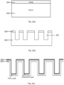
- Figures 1(a) and 1(b) illustrate steps of manufacturing trenches with asymmetric insulation layers, according to the state of the art.
- the manufacturing process starts with a homogenous thick oxide insulation layer, covered by a photoresist material.
- the photoresist is exposed to remove the photoresist to a desired depth, X .
- the exposure dose is used to determine the depth X , and thus determines where thin gate oxide will be formed.
- An etch solution is then used to remove the thick oxide layer over all exposed areas.
- This method of manufacture results in large variation of X from wafer to wafer and die to die on a wafer. There is also reduced integrity and stability of the photoresist within the trench during the etch process.
- US 2010/059816 A1 discloses a method of manufacturing a semiconductor device having trenches, comprising a step of forming a photoresist reinforcement film on a silicon oxide film in the trenches.
- the photoresist reinforcement film prevents the silicon oxide film to be left from being removed by an etching solution entering the interface of a photoresist layer and the silicon oxide film in a wet etching process.
- the photoresist reinforcement film is preferably made of a silicon nitride film and the thickness is about 60 nm.
- Forming a first insulation layer may comprise forming a thick insulation layer, and the hydrophilic layer may be deposited over the thick insulation layer, and forming a second insulation layer may comprise forming a thin insulation layer on the sidewall of the first side of the one or more trenches, wherein the thin insulation layer is thinner than the thick insulation layer.
- forming a first insulation layer may comprise forming a thin insulation layer
- forming a second insulation layer may comprise forming a thick insulation layer over the thin insulation layer, wherein the thin insulation layer is thinner than the thick insulation layer.
- the presently disclosed method of manufacturing a semiconductor device includes a step of depositing a hydrophilic layer.
- the hydrophilic layer means that the etchant, in the later step of performing a wet etch, uses capillary action to etch the insulation layer on the sidewalls, below the surface of the photoresist material.
- the capillary action etches down a channel between the hydrophilic layer and the material (for example, silicon) of the semiconductor device outside the trench. This also allows etching below the surface of the insulation layer, allowing deeper channels to be etched. Furthermore, this helps to achieve uniformity and consistency in both the etching process and the width and depth of the etched portion of the insulation layer. This also increases the controllability of the manufacturing process, in particular the width and depth of the etched portion.
- the disclosed manufacturing process includes performing a wet etch that etches down a channel along the sidewall of the trench. This process facilitates the manufacture of devices having trenches with asymmetric or symmetric trench gate regions, having two different insulation layer thicknesses on a sidewall of a trench.
- the herein disclosed manufacturing process improves uniformity of channel etch depth and width, and therefore improves electrical performance uniformity from die to die.
- the disclosed process also has improved process control and yield.
- the disclosed process results in a reduced number of defects caused by instability of photoresist during wet etch down deep trenches, compared to state-of-the-art methods of manufacturing trenches.
- the method may be used to process devices of Silicon, SiC, GaN, and other materials used in semiconductor devices.
- the method may be used to manufacture insulated gate bipolar transistors (IGBTs), metal oxide semiconductor field-effect transistors (MOSFETs), MOS-Controlled Thyristors, or other semiconductor power devices.
- IGBTs insulated gate bipolar transistors
- MOSFETs metal oxide semiconductor field-effect transistors
- Thyristors MOS-Controlled Thyristors
- Depositing a photoresist material may be a two-step process that includes depositing a photoresist material and then exposing the hydrophilic layer on an upper region of a first side of the one or more trenches.
- the method may further comprise depositing a filling material after growing the thin insulation layer.
- the hydrophilic layer may comprise Si x N y (silicon nitride) with good wettability or a high degree of wetting
- Si x N y silicon nitride
- the wettability modulates etch rate down trench side-walls, and enables uniformity of etch distance and repeatability of the process. If wettability is not sufficient, some areas will etch faster than others down the trench walls by the capillary action. A material with high degree of wetting improves the capillary action that etches down a channel.
- the wettability property of the hydrophilic layer allows accurate control of etch depth and ensures uniformity of the etch process down the etched channel.
- the thickness of the hydrophilic layer mains integrity during the wet etch/capillary etch process.
- the step of performing a wet etch may be carried out using a buffered oxide etch (BOE).
- BOE buffered oxide etch
- the semiconductor device or wafer may be immersed in the BOE in order to etch the insulation layer along any exposed mesa region and trench sidewalls. Exposure to the bottom of deep trenches is difficult except for very wide trenches.
- the use of a wet etch means that exposure to the bottom of the trench is not required.
- the wet etch makes use of capillary action of the etch solution (such as BOE 7:1 HCL) to etch down the exposed sidewall and up the second trench sidewall to a desired distance.
- the buffered oxide etch may comprise hydrofluoric (HF) acid.
- Hydrofluoric acid is a suitable solution for use in semiconductor manufacturing, and provides sufficient etch rate to make the process manufacturable.
- Forming a thick insulation layer may comprise thermally growing a thick oxide layer using a local oxidation of silicon process.
- forming a thick insulation layer may comprise depositing a thick oxide layer.
- Depositing a thick oxide layer may be carried out using Tetraethyl Orthosilicate (TEOS) deposition.
- TEOS deposition is very conformal.
- Growing a thin insulation layer may comprise thermally growing a thin oxide layer at 900°C to 1100°C.
- the thin insulation layer may have a thickness between 500 ⁇ to 1800 ⁇ .
- the method may comprise manufacturing one or more trenches with an asymmetric insulation layer.
- the one or more trenches may have one sidewall with an insulation layer of two different thicknesses, and one sidewall with an insulation layer of constant thickness.
- the step of performing the wet etch may be used to etch along only one sidewall of the one or more trenches.
- the method may comprise manufacturing one or more trenches with a symmetric insulation layer.
- the one or more trenches may have both sidewalls each with an insulation layer of two different thicknesses.
- Depositing a photoresist material may comprise exposing the hydrophilic layer on an upper region of two sides of the one or more trenches.
- the method may further comprise performing the wet etch process to etch the insulation layer on two sidewalls of the one or more trenches to a predetermined distance below a surface of the photoresist material, and growing a thin insulation layer on the two sidewalls of the one or more trenches.
- the method may comprise manufacturing at least two trenches each with an insulation layer.
- a first trench may be separated from a second trench by a mesa region between the two trenches.
- the first side of the first trench may be adjacent to the first side of the second trench.
- Depositing a photoresist material may comprise exposing the hydrophilic layer in the mesa region between the first and second trenches.
- the method may further comprise removing the hydrophilic layer in the mesa region between the two trenches. This allows the thick oxide in the mesa region to be removed by etching, as the thick oxide in the mesa region is therefore not protected by the hydrophilic layer. This also removes the hydrophilic layer above the thick oxide on the trench sidewall so that the thick oxide on the sidewall can be etched.
- Removing the hydrophilic layer in the mesa region may comprise removing the hydrophilic layer such that a top surface of the hydrophilic layer is recessed relative to a surface of the thick oxide layer.
- the method may further comprise performing a wet etch process to etch the insulation layer on the mesa region. This removes the thick insulation layer on the mesa region.
Landscapes
- Element Separation (AREA)
- Weting (AREA)
Description
- The present disclosure relates to a method of manufacturing a semiconductor device having an insulation layer on selective trench sidewalls.
- Many applications use fast switching, low loss insulated gate bipolar transistors (IGBTs) or metal oxide semiconductor field-effect transistors (MOSFETs). Trench gate IGBTs with uniform thin oxide have high turn on energy (EON) and turn off energy (EOFF) losses due to high gate collector capacitance (Ccc) and gate emitter capacitance (CCG).
- Asymmetric trench oxide (thin oxide in a portion of one trench sidewall and thick oxide in the remaining areas) to improve performance in trench gate IGBTs and MOSFETs with Silicon and SiC. For example, within IGBTs it is advantageous to provide thick oxide in trench sidewall regions not used as a conduction channel and to provide thin oxide in regions where conduction channels are formed. This reduces the gate collector capacitance (Ccc) and gate emitter capacitance (CGE)and improves the switching speed. This also reduces the turn on energy loss (EON) and the turn off energy loss (EOFF). In the case of SiC where electric field is 10X higher that silicon, the gate structure also enhance breakdown voltage (BV) capability.
- Currently available processes for manufacturing a trench with a non-constant oxide layer are unreliable and result in low yields.
- Traditional processing methods rely on using the photolithographic exposure dose to determine etch depth. Due to inherent inaccuracy, the etch depth has the tendency to vary significantly from one site to another across a wafer, from wafer to wafer, and between batches.
- "IGBT with superior long-term switching behaviour by asymmetric trench oxide", Proceedings of the 30th International Symposium on Power Semiconductor Devices & ICs 2018, pp 24-27 relates to an IGBT chip with a trench having an asymmetric thick oxide layer and process for manufacturing the chip.
-
Figures 1(a) and 1(b) illustrate steps of manufacturing trenches with asymmetric insulation layers, according to the state of the art. The manufacturing process starts with a homogenous thick oxide insulation layer, covered by a photoresist material. The photoresist is exposed to remove the photoresist to a desired depth, X. The exposure dose is used to determine the depth X, and thus determines where thin gate oxide will be formed. An etch solution is then used to remove the thick oxide layer over all exposed areas. - This method of manufacture results in large variation of X from wafer to wafer and die to die on a wafer. There is also reduced integrity and stability of the photoresist within the trench during the etch process.
-
US 2010/059816 A1 discloses a method of manufacturing a semiconductor device having trenches, comprising a step of forming a photoresist reinforcement film on a silicon oxide film in the trenches.The photoresist reinforcement film prevents the silicon oxide film to be left from being removed by an etching solution entering the interface of a photoresist layer and the silicon oxide film in a wet etching process. The photoresist reinforcement film is preferably made of a silicon nitride film and the thickness is about 60 nm. - Aspects and preferred features are set out in the accompanying claims.
- According to the present disclosure, there is provided a method of manufacturing a semiconductor device having one or more trenches with an insulation according to claim 1.
- Preferred embedments are disclosed in the dependent claims.
- Forming a first insulation layer may comprise forming a thick insulation layer, and the hydrophilic layer may be deposited over the thick insulation layer, and forming a second insulation layer may comprise forming a thin insulation layer on the sidewall of the first side of the one or more trenches, wherein the thin insulation layer is thinner than the thick insulation layer.
- Alternatively, forming a first insulation layer may comprise forming a thin insulation layer, and forming a second insulation layer may comprise forming a thick insulation layer over the thin insulation layer, wherein the thin insulation layer is thinner than the thick insulation layer.
- The presently disclosed method of manufacturing a semiconductor device includes a step of depositing a hydrophilic layer. The hydrophilic layer means that the etchant, in the later step of performing a wet etch, uses capillary action to etch the insulation layer on the sidewalls, below the surface of the photoresist material. The capillary action etches down a channel between the hydrophilic layer and the material (for example, silicon) of the semiconductor device outside the trench. This also allows etching below the surface of the insulation layer, allowing deeper channels to be etched. Furthermore, this helps to achieve uniformity and consistency in both the etching process and the width and depth of the etched portion of the insulation layer. This also increases the controllability of the manufacturing process, in particular the width and depth of the etched portion.
- The disclosed manufacturing process includes performing a wet etch that etches down a channel along the sidewall of the trench. This process facilitates the manufacture of devices having trenches with asymmetric or symmetric trench gate regions, having two different insulation layer thicknesses on a sidewall of a trench.
- The herein disclosed manufacturing process improves uniformity of channel etch depth and width, and therefore improves electrical performance uniformity from die to die. The disclosed process also has improved process control and yield. The disclosed process results in a reduced number of defects caused by instability of photoresist during wet etch down deep trenches, compared to state-of-the-art methods of manufacturing trenches.
- The method may be used to process devices of Silicon, SiC, GaN, and other materials used in semiconductor devices.
- The method may be used to manufacture insulated gate bipolar transistors (IGBTs), metal oxide semiconductor field-effect transistors (MOSFETs), MOS-Controlled Thyristors, or other semiconductor power devices.
- Depositing a photoresist material may be a two-step process that includes depositing a photoresist material and then exposing the hydrophilic layer on an upper region of a first side of the one or more trenches.
- The method may further comprise depositing a filling material after growing the thin insulation layer.
- The hydrophilic layer may comprise SixNy (silicon nitride) with good wettability or a high degree of wetting The wettability modulates etch rate down trench side-walls, and enables uniformity of etch distance and repeatability of the process. If wettability is not sufficient, some areas will etch faster than others down the trench walls by the capillary action. A material with high degree of wetting improves the capillary action that etches down a channel. The wettability property of the hydrophilic layer allows accurate control of etch depth and ensures uniformity of the etch process down the etched channel.
- The thickness of the hydrophilic layer mains integrity during the wet etch/capillary etch process.
- The step of performing a wet etch may be carried out using a buffered oxide etch (BOE). The semiconductor device or wafer may be immersed in the BOE in order to etch the insulation layer along any exposed mesa region and trench sidewalls. Exposure to the bottom of deep trenches is difficult except for very wide trenches. The use of a wet etch means that exposure to the bottom of the trench is not required. The wet etch makes use of capillary action of the etch solution (such as BOE 7:1 HCL) to etch down the exposed sidewall and up the second trench sidewall to a desired distance.
- The buffered oxide etch may comprise hydrofluoric (HF) acid. Hydrofluoric acid is a suitable solution for use in semiconductor manufacturing, and provides sufficient etch rate to make the process manufacturable.
- Forming a thick insulation layer may comprise thermally growing a thick oxide layer using a local oxidation of silicon process.
- Alternatively, forming a thick insulation layer may comprise depositing a thick oxide layer.
- Depositing a thick oxide layer may be carried out using Tetraethyl Orthosilicate (TEOS) deposition. TEOS deposition is very conformal.
- The thick insulation layer may have a thickness between 1800Å and 5000Å, whereby 1Å = 0.1nm.
- Growing a thin insulation layer may comprise thermally growing a thin oxide layer at 900°C to 1100°C.
- The thin insulation layer may have a thickness between 500Å to 1800Å.
- The method may comprise manufacturing one or more trenches with an asymmetric insulation layer. The one or more trenches may have one sidewall with an insulation layer of two different thicknesses, and one sidewall with an insulation layer of constant thickness. The step of performing the wet etch may be used to etch along only one sidewall of the one or more trenches.
- Alternatively or additionally, the method may comprise manufacturing one or more trenches with a symmetric insulation layer. The one or more trenches may have both sidewalls each with an insulation layer of two different thicknesses. Depositing a photoresist material may comprise exposing the hydrophilic layer on an upper region of two sides of the one or more trenches. The method may further comprise performing the wet etch process to etch the insulation layer on two sidewalls of the one or more trenches to a predetermined distance below a surface of the photoresist material, and growing a thin insulation layer on the two sidewalls of the one or more trenches.
- The method may comprise manufacturing at least two trenches each with an insulation layer. A first trench may be separated from a second trench by a mesa region between the two trenches. The first side of the first trench may be adjacent to the first side of the second trench. Depositing a photoresist material may comprise exposing the hydrophilic layer in the mesa region between the first and second trenches.
- The method may further comprise removing the hydrophilic layer in the mesa region between the two trenches. This allows the thick oxide in the mesa region to be removed by etching, as the thick oxide in the mesa region is therefore not protected by the hydrophilic layer. This also removes the hydrophilic layer above the thick oxide on the trench sidewall so that the thick oxide on the sidewall can be etched.
- Removing the hydrophilic layer in the mesa region may comprise removing the hydrophilic layer such that a top surface of the hydrophilic layer is recessed relative to a surface of the thick oxide layer.
- The method may further comprise performing a wet etch process to etch the insulation layer on the mesa region. This removes the thick insulation layer on the mesa region.
- The present disclosure will be understood, by way of example only, from the detailed description that follows and from the accompanying drawings in which:
-
Figures 1(a) and 1(b) illustrate steps of manufacturing trenches with asymmetric insulation layers, according to the state of the art; -
Figures 2(a) to 2(j) illustrate steps of manufacturing trenches with asymmetric insulation layers, according to an embodiment of the disclosure; -
Figure 3 illustrates schematically a semiconductor device having trenches manufactured using a method according to an embodiment of the disclosure; -
-
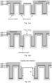
Figures 2(a) to 2(j) illustrate steps within the manufacturing process of trenches with asymmetric insulation layers, according to an embodiment of the disclosure. -
Figure 2(a) illustrates the first step of manufacturing two trenches with asymmetric insulation layers, which is as follows:- (a) Step 1
- A
thin oxide layer 204 is deposited on asilicon substrate 206. The thin oxide layer has thickness of approximately 500Å to 1800Å.
- A
- (a) Step 1
-
Figure 2(b) illustrates the second step of manufacturing two trenches, which is as follows:
(b) Step 2- Photolithography and then a dry etch step using plasma source to form trenches to desired depth z in the
silicon substrate 206. In this embodiment, the desired depth z of the trenches is 3µm to 6µm.
- Photolithography and then a dry etch step using plasma source to form trenches to desired depth z in the
-
Figure 2(c) illustrates the third step of manufacturing two trenches, which is as follows:
(c) Step 3- A
thick oxide layer 204 is thermally grown or deposited on the sidewalls and bottom surface of the trenches. Thethick oxide layer 204 may be deposited using TEOS. The thick oxide layer has a thickness of approximately 1800Å to 5000Å. - A
hydrophilic layer 206 such as nitride is deposited over theoxide layer 204. Thenitride layer 206 has a thickness of approximately 1000Å to 2500Å.
- A
-
Figure 2(d) illustrates the fourth step of manufacturing two trenches, which is as follows:
(d) Step 4- The trenches are filled with a
photoresist material 208. - The
photoresist 208 is deposited such that thehydrophilic layer 206 is exposed on a first side of each trench for which asymmetric oxide will be manufactured, and in the mesa region between trenches. - The first side of each trench (the side where the
hydrophilic layer 206 is exposed) is the side of the trench that will be manufactured to have a thin oxide layer, whilst the side of each trench that will be manufactured to have thick oxide remains covered by the photoresist. - The thickness of the photoresist is 1.0µm to 1.5µm for a 1.5µm width trench.
- The trenches are filled with a
-
Figure 2(e) illustrates the fifth step of manufacturing two trenches, which is as follows:
(e) Step 5- An etch process is performed on the exposed
hydrophilic layer 206. The etch process can be a wet or dry etch, and stops on thethick oxide layer 204 in the mesa region. - Since the
hydrophilic layer 206 comprises nitride, the etch process may be done in plasma ambient (an atmosphere or environment of plasma, created by a mixture of gases) using CF4/HBr chemistry. - The
hydrophilic layer 206 is etched such that the edges of thehydrophilic layer 206 are recessed relative to the surface of thethick oxide 204.
- An etch process is performed on the exposed
-
Figure 2(f) illustrates the sixth step of manufacturing two trenches, which is as follows:
(f) Step 6- The whole wafer is immersed in a BOE (buffered oxide etch) such as 7:1 HF. The buffered oxide etchant etches the
oxide layer 204 on the exposed mesa region and the trench sidewalls extending down from the exposed mesa region to a desired depth Y below the surface of the trench. - The
hydrophilic layer 206 creates a capillary action so that the etchant etches theoxide layer 204 along the narrow channel between the hydrophilic layer itself 206 and thesilicon 202. - The presence of the
hydrophilic layer 206 allows control of the etch depth and uniformity of the etch process. Thehydrophilic layer 206 reduces defects formed during the etch process.
- The whole wafer is immersed in a BOE (buffered oxide etch) such as 7:1 HF. The buffered oxide etchant etches the
-
Figure 2(g) illustrates the seventh step of manufacturing two trenches, which is as follows:
(g)Step 7- The photoresist is stripped (removed) using any suitable wet (such as hot phosphoric acid) or dry (such as a mixture of CF4 and HBr gases in a plasma etch chamber) chemistry.
-
Figure 2(h) illustrates the eighth step of manufacturing two trenches, which is as follows:
(h) Step 8- The hydrophilic layer is stripped (removed) using any suitable wet or dry chemistry. This leaves the trenches having
only oxide 204 on regions not exposed in Steps 4 and 5.
- The hydrophilic layer is stripped (removed) using any suitable wet or dry chemistry. This leaves the trenches having
-
Figure 2(i) illustrates the ninth step of manufacturing two trenches, which is as follows:- (i) Step 9
- A
thin oxide layer 210 is grown on the exposed silicon in a furnace step at 900°C to 1100°C. The thin oxide layer grows on the first side of each trench in which the hydrophilic layer was exposed in Step 4, and in the mesa region between the trenches. - The thin oxide layer has thickness of approximately 500Å to 1800Å.
- A
- (i) Step 9
-
Figure 2(j) illustrates the tenth step of manufacturing two trenches, which is as follows:
(j) Step 10-
Polysilicon 212 is deposited to fill the trenches. Thepolysilicon 212 is planarised by etching the top of thepolysilicon 212 to level off with thesilicon 202 in the mesa region between the trenches.
-
-
Figure 3 illustrates schematically a semiconductor device having trenches manufactured using a method according to an embodiment of the disclosure. In this device, the active gates T1, each have asymmetric trench oxide insulation layers, whilst the dummy (or auxiliary trenches) T2 have symmetric thick oxide insulation layers.
The active trenches T1 shown in this embodiment each have an asymmetric oxide. In this embodiment only the electron conduction channel region hasthin oxide 210, and the remaining sidewall and bottom of each of the active trenches T1 havethick oxide 204. Thethin oxide 210 in the channel region reduces the input capacitance (Cin) and CGC. This results in reduced gate charge and faster turn-off and turn-on times, therefore reducing EON and EOFF respectively.
Whilst the auxiliary trenches T2 are shown as havingthick oxide insulation 204, alternatively the disclosed method could be used to manufacture a semiconductor device having auxiliary trenches with symmetric thin oxide or having variable oxide thickness. -
Figures 4(a) to 4(i) shows steps in the manufacturing method of a semiconductor device, according to an embodiment of the disclosure; -
Figure 4(a) illustrates the first step of manufacturing the trenches of the semiconductor device, which is as follows:- (a) Step 1
-
Trenches 905 are etched. - An
initial oxide layer 910 is formed over the trenches. Theinitial oxide layer 910 is a sacrificial oxidation layer. It is an oxide layer created immediately after silicon etch to create trenches. The main purpose of this layer is to remove surface roughness created by the trench etch process. Traditionally, this oxide is later removed prior to formation of the thin gate oxide. - A
hydrophilic layer 915 such as nitride is deposited over theinitial oxide layer 910. Thenitride layer 915 has a thickness of approximately 1000Å to 2500Å. - A
thin oxide layer 920 is deposited using TEOS over thehydrophilic layer 915. Thethin oxide layer 920 has thickness of approximately 500Å to 1800Å.
-
- (a) Step 1
-
Figures 4(b) and 4(c) illustrates the second step of manufacturing the trenches of the semiconductor device, which is as follows:
(b) Step 2- Photolithography is performed to apply a
photoresist mask 925 that fills the trenches, where the mask ends in the centre of one trench 930 (for example, the active trench) and at least one other trench 935 (for example, a dummy trench). This leaves half of the active trench and the dummy trench exposed, as well as the mesa region between the trenches. Themask 925 may be applied in a two-step process as shown in which the mask is deposited and then etched to expose theTEOS 920. - The
photoresist 925 is deposited such that thethin oxide layer 920 is exposed on a first side of each trench for which asymmetric oxide will be manufactured, and in themesa region 940 between trenches. - The first side of each trench (the side where the
thin oxide layer 920 is exposed) is the side of the trench that will be manufactured to have a thick oxide layer, whilst the side of each trench that will be manufactured to have thin oxide or oxide of different thickness remains covered by the photoresist.
- Photolithography is performed to apply a
-
Figure 4(d) illustrates the first step of manufacturing the trenches of the semiconductor device, which is as follows:
(d) Step 3- A capillary wet etch is performed on the
thin oxide layer 920. The etch may be performed by immersing the whole wafer in a BOE (buffered oxide etch) such as 7:1 HF. The buffered oxide etchant etches theoxide layer 920 on the exposedmesa region 940, the exposed trench sidewalls and bottom, and the trench sidewalls extending up from the trench bottom to a desired height Y above the bottom surface of the trench. - The
hydrophilic layer 915 creates a capillary action so that the etchant etches theoxide layer 920 along the narrow channel between thehydrophilic layer 915 itself and thephotoresist 925. - The presence of the
hydrophilic layer 915 allows control of the etch depth and uniformity of the etch process. Thehydrophilic layer 915 reduces defects formed during the etch process.
- A capillary wet etch is performed on the
-
Figure 4(e) illustrates the first step of manufacturing the trenches of the semiconductor device, which is as follows:
(e) Step 4- The photoresist is stripped (removed) using any suitable wet or dry chemistry.
- An etch process is performed to remove the exposed regions of the
hydrophilic layer 915. The etch process can be a wet or dry etch, and stops on theinitial oxide layer 910. - Since the
hydrophilic layer 915 comprises nitride, the etch process may be done in plasma ambient using CF4/HBr chemistry.
-
Figure 4(f) illustrates the first step of manufacturing the trenches of the semiconductor device, which is as follows:
(f) Step 5- A
thick oxide layer 945 is thermally grown or deposited on the sidewalls and bottom surface of the trenches in areas without thehydrophilic layer 915 remaining. Thethick oxide layer 945 may be deposited using loyal oxidation of silicon (LOCOS). Thethick oxide layer 945 has a thickness of approximately 1800Å to 5000Å.
- A
-
Figure 4(g) illustrates the first step of manufacturing the trenches of the semiconductor device, which is as follows:
(g) Step 6- An etch process is performed to remove the remaining regions of the
hydrophilic layer 915 and the remainingTEOS 920.
- An etch process is performed to remove the remaining regions of the
-
Figure 4(h) illustrates the first step of manufacturing the trenches of the semiconductor device, which is as follows:
(h)Step 7- Photolithography is performed to apply a
photoresist mask 950 that fills theactive trench 930, where the mask leaves thedummy trenches 935 exposed. - A wet etch process is performed that strips the
dummy trenches 935 to the silicon layer.
- Photolithography is performed to apply a
-
Figure 4(i) illustrates the first step of manufacturing the trenches of the semiconductor device, which is as follows:- (i) Step 8
- A
thin oxidation layer 955 is grown on the dummy trenches having a constant thickness on the sidewalls and bottom surfaces. Thethin oxide 955 layer may be is grown in a furnace step at 900°C to 1100°C. Thethin oxide layer 955 has thickness of approximately 500Å to 1800Å. - The photoresist is stripped (removed) using any suitable wet or dry chemistry.
-
Polysilicon 960 is deposited to fill the trenches. Thepolysilicon 960 is planarised by etching the top of thepolysilicon 960 to level off with the silicon in the mesa region between the trenches.
- A
- (i) Step 8
-
Figure 5 shows an example of a semiconductor device manufactured using the steps ofFigures 4(a) to 4(h) . - The skilled person will understand that in the preceding description and appended claims, positional terms such as 'above', 'overlap', 'under', 'lateral', etc. are made with reference to conceptual illustrations of an apparatus, such as those showing standard cross-sectional perspectives and those shown in the appended drawings. These terms are used for ease of reference and are therefore to be understood as referring to a device when in an orientation as shown in the accompanying drawings.
- It will be appreciated that all doping polarities mentioned above could be reversed, the resulting devices still being in accordance with embodiments of the present invention.
- Although the disclosure has been described in terms of preferred embodiments as set forth above, it should be understood that these embodiments are illustrative. Those skilled in the art will be able to make modifications and alternatives in view of the disclosure, which are contemplated as long as they fall within the scope of the appended claims.
Claims (15)
- A method of manufacturing a semiconductor device having one or more trenches (205, 905) with an insulation layer (204), wherein the one or more trenches with an insulation layer are manufactured using the steps of:i) performing an etching process to form the one or more trenches, whereby the trenches are formed in an upper surface of a substrate (202) extending downwards in the substrate from its upper surface;ii) forming a first insulation layer (204) on the upper surface of the substrate and a lower surface and sidewalls of the one or more trenches;iii) depositing a hydrophilic layer (206, 915) over the first insulation layer, wherein the hydrophilic layer comprises nitride and the hydrophilic layer has a thickness between 100nm and 250nmiv) depositing a photoresist material (208, 925) in the one or more trenches, wherein depositing a photoresist material comprises exposing the hydrophilic layer on an upper region of a first side of the one or more trenches, leaving the hydrophilic layer not in the upper region covered with the deposited photoresist material;v) performing a capillary wet etch process to etch the insulation layer on the sidewall of the first side of the one or more trenches to a predetermined distance below a surface of the photoresist material;vi) removing the photoresist material;vii) removing the hydrophilic layer; andafter performing the wet etch process, removing the photoresist material, and removing the hydrophilic layer; viii) forming a second insulation (210, 945) layer on the sidewall of the first side of the one or more trenches.
- A method according to claim 1, wherein forming a first insulation layer comprises forming a thick insulation layer (204), and
wherein the hydrophilic layer is deposited over the thick insulation layer, and
wherein forming a second insulation layer comprises forming a thin insulation layer (210) on the sidewall of the first side of the one or more trenches, wherein the thin insulation layer is thinner than the thick insulation layer. - A method according to claim 1, wherein forming a first insulation layer comprises forming a thin insulation layer, and wherein forming a second insulation layer comprises forming a thick insulation layer (945) over the thin insulation layer, wherein the thin insulation layer is thinner than the thick insulation layer.
- A method according to claim 2,
wherein the method further comprises depositing a filling material (212, 960) after growing the thin insulation layer. - A method according to any preceding claim, wherein the step of performing a wet etch is carried out using a buffered oxide etch, optionally wherein the buffered oxide etch comprises hydrofluoric acid.
- A method according to any preceding claim, wherein forming the insulation layer comprises thermally growing a thick oxide layer using a local oxidation of silicon process.
- A method according to any of claims 1 to 5, wherein forming the insulation layer comprises depositing a thick oxide layer.
- A method according to claim 7, wherein depositing the thick oxide layer is carried out using Tetraethyl Orthosilicate, TEOS.
- A method according to claims 2 to 8, wherein growing the thin insulation layer comprises thermally growing a thin oxide layer at 900°C to 1100°C, wherein the thin insulation layer has a thickness between 50nm and 180nm.
- A method according to any preceding claim, wherein the insulation is asymmetric.
- A method according to any preceding claim, wherein the insulation is symmetric, andwherein depositing the photoresist material comprises exposing the hydrophilic layer on the upper region of two sides of the one or more trenches, andwherein the method further comprises:performing the capillary wet etch process to etch the insulation layer on two sidewalls of the one or more trenches to a predetermined distance below Z the surface of the photoresist material; andgrowing the insulation layer on the two sidewalls of the one or more trenches.
- A method according to any preceding claim, wherein a first trench is separated from a second trench by a mesa region between the two trenches; andwherein the first side of the first trench is adjacent to the first side of the second trench; andwherein depositing the photoresist material comprises exposing the hydrophilic layer in the upper region formed by mesa region between the first and second trenches
- A method according to claim 12, wherein the method further comprises removing the hydrophilic layer in the mesa region between the two trenches.
- A method according to claim 13, wherein removing the hydrophilic layer in the mesa region comprises removing the hydrophilic layer such that a top surface of the hydrophilic layer is recessed relative to a surface of the insulating layer deposited as a thick oxide layer
- A method according to any of claims 12, 13, or 14, wherein the method further comprises performing the capllary wet etch process to etch the insulation layer on the mesa region.
Applications Claiming Priority (1)
| Application Number | Priority Date | Filing Date | Title |
|---|---|---|---|
| PCT/EP2020/066909 WO2021254618A1 (en) | 2020-06-18 | 2020-06-18 | Method of forming asymmetric thickness oxide trenches |
Publications (2)
| Publication Number | Publication Date |
|---|---|
| EP3944740A1 EP3944740A1 (en) | 2022-02-02 |
| EP3944740B1 true EP3944740B1 (en) | 2024-06-19 |
Family
ID=71105492
Family Applications (1)
| Application Number | Title | Priority Date | Filing Date |
|---|---|---|---|
| EP20733614.0A Active EP3944740B1 (en) | 2020-06-18 | 2020-06-18 | Method of forming asymmetric thickness oxide trenches |
Country Status (4)
| Country | Link |
|---|---|
| US (1) | US20220320310A1 (en) |
| EP (1) | EP3944740B1 (en) |
| CN (1) | CN114586134A (en) |
| WO (1) | WO2021254618A1 (en) |
Family Cites Families (8)
| Publication number | Priority date | Publication date | Assignee | Title |
|---|---|---|---|---|
| KR100858556B1 (en) * | 2000-08-08 | 2008-09-16 | 마이크로세미 코포레이션 | Power MOOS Device with an Asymmetric Channel Structure |
| US6444528B1 (en) * | 2000-08-16 | 2002-09-03 | Fairchild Semiconductor Corporation | Selective oxide deposition in the bottom of a trench |
| US6674124B2 (en) * | 2001-11-15 | 2004-01-06 | General Semiconductor, Inc. | Trench MOSFET having low gate charge |
| GB0405325D0 (en) * | 2004-03-10 | 2004-04-21 | Koninkl Philips Electronics Nv | Trench-gate transistors and their manufacture |
| KR100829594B1 (en) * | 2006-10-10 | 2008-05-14 | 삼성전자주식회사 | Slurry composition for chemical mechanical polishing and manufacturing method of semiconductor memory device using same |
| JP2009088188A (en) * | 2007-09-28 | 2009-04-23 | Sanyo Electric Co Ltd | Trench gate type transistor and manufacturing method thereof |
| US8772865B2 (en) * | 2012-09-26 | 2014-07-08 | Semiconductor Components Industries, Llc | MOS transistor structure |
| US11569371B2 (en) * | 2017-05-25 | 2023-01-31 | Dynex Semiconductor Limited | Semiconductor device |
-
2020
- 2020-06-18 WO PCT/EP2020/066909 patent/WO2021254618A1/en not_active Ceased
- 2020-06-18 EP EP20733614.0A patent/EP3944740B1/en active Active
- 2020-06-18 CN CN202080007135.4A patent/CN114586134A/en active Pending
- 2020-06-18 US US17/312,597 patent/US20220320310A1/en not_active Abandoned
Also Published As
| Publication number | Publication date |
|---|---|
| CN114586134A (en) | 2022-06-03 |
| WO2021254618A1 (en) | 2021-12-23 |
| US20220320310A1 (en) | 2022-10-06 |
| EP3944740A1 (en) | 2022-02-02 |
Similar Documents
| Publication | Publication Date | Title |
|---|---|---|
| US12317561B2 (en) | SIC MOSFET structures with asymmetric trench oxide | |
| CN100481503C (en) | Trench gate transistor and fabrication thereof | |
| US6444528B1 (en) | Selective oxide deposition in the bottom of a trench | |
| TW201631634A (en) | Tapered gate oxide in laterally diffused MOS devices | |
| US9953971B2 (en) | Insulated gate bipolar transistor (IGBT) and related methods | |
| CN111403289B (en) | Manufacturing method of split gate MOSFET | |
| CN110896026A (en) | Trench MOSFET structure and method of making the same | |
| US20220320322A1 (en) | Igbt with a variation of trench oxide thickness regions | |
| US20240379823A1 (en) | Bevel structure and its manufacturing method, ldmos structure and its manufacturing method | |
| JP5105835B2 (en) | Protrusion type transistor manufacturing method | |
| CN108470737B (en) | Three-dimensional memory and manufacturing method thereof | |
| JP3965027B2 (en) | Method for manufacturing trench gate type MIS device having thick polysilicon insulating layer at bottom of trench | |
| US20240178289A1 (en) | Mosfet gate formation | |
| CN114744044A (en) | Trench type silicon carbide MOSFET of triple-protection gate oxide layer and preparation method thereof | |
| CN104253050B (en) | A kind of manufacture method of grooved lateral MOSFET device | |
| CN114156183A (en) | Split gate power MOS device and manufacturing method thereof | |
| CN114823877A (en) | trench gate semiconductor device | |
| TWI686850B (en) | Semiconductor device and method of fabricating the same | |
| US20220320310A1 (en) | Method of forming asymmetric thickness oxide trenches | |
| CN109427808B (en) | Semiconductor memory element and method of manufacturing the same | |
| CN112993014B (en) | Silicon carbide planar power semiconductor device and manufacturing method thereof | |
| CN114743879A (en) | Manufacturing method of split gate MOSFET | |
| CN113471075A (en) | Semiconductor device and method of forming the same | |
| US20260032981A1 (en) | Self-align multi trench mosfet and manufacturing method of the same | |
| CN110379850B (en) | Trench Power Transistor Manufacturing Method |
Legal Events
| Date | Code | Title | Description |
|---|---|---|---|
| STAA | Information on the status of an ep patent application or granted ep patent |
Free format text: STATUS: UNKNOWN |
|
| STAA | Information on the status of an ep patent application or granted ep patent |
Free format text: STATUS: THE INTERNATIONAL PUBLICATION HAS BEEN MADE |
|
| PUAI | Public reference made under article 153(3) epc to a published international application that has entered the european phase |
Free format text: ORIGINAL CODE: 0009012 |
|
| STAA | Information on the status of an ep patent application or granted ep patent |
Free format text: STATUS: REQUEST FOR EXAMINATION WAS MADE |
|
| 17P | Request for examination filed |
Effective date: 20210527 |
|
| AK | Designated contracting states |
Kind code of ref document: A1 Designated state(s): AL AT BE BG CH CY CZ DE DK EE ES FI FR GB GR HR HU IE IS IT LI LT LU LV MC MK MT NL NO PL PT RO RS SE SI SK SM TR |
|
| RAP3 | Party data changed (applicant data changed or rights of an application transferred) |
Owner name: ZHUZHOU CRRC TIMES SEMICONDUCTOR CO. LTD Owner name: DYNEX SEMICONDUCTOR LIMITED |
|
| P01 | Opt-out of the competence of the unified patent court (upc) registered |
Effective date: 20230528 |
|
| DAV | Request for validation of the european patent (deleted) | ||
| DAX | Request for extension of the european patent (deleted) | ||
| REG | Reference to a national code |
Ref legal event code: R079 Ipc: H01L0029660000 Ref country code: DE Ref document number: 602020032625 Country of ref document: DE Free format text: PREVIOUS MAIN CLASS: H01L0021316000 |
|
| RIC1 | Information provided on ipc code assigned before grant |
Ipc: H01L 29/739 20060101ALI20231201BHEP Ipc: H01L 29/423 20060101ALI20231201BHEP Ipc: H01L 29/417 20060101ALI20231201BHEP Ipc: H01L 29/40 20060101ALI20231201BHEP Ipc: H01L 29/06 20060101ALI20231201BHEP Ipc: H01L 29/66 20060101AFI20231201BHEP |
|
| GRAP | Despatch of communication of intention to grant a patent |
Free format text: ORIGINAL CODE: EPIDOSNIGR1 |
|
| STAA | Information on the status of an ep patent application or granted ep patent |
Free format text: STATUS: GRANT OF PATENT IS INTENDED |
|
| RAP3 | Party data changed (applicant data changed or rights of an application transferred) |
Owner name: ZHUZHOU CRRC TIMES SEMICONDUCTOR CO. LTD Owner name: DYNEX SEMICONDUCTOR LIMITED |
|
| INTG | Intention to grant announced |
Effective date: 20240112 |
|
| RIN1 | Information on inventor provided before grant (corrected) |
Inventor name: HUTCHINGS, JOHN Inventor name: DEVINY, IAN Inventor name: NGWENDSON, LUTHER-KING |
|
| GRAS | Grant fee paid |
Free format text: ORIGINAL CODE: EPIDOSNIGR3 |
|
| GRAA | (expected) grant |
Free format text: ORIGINAL CODE: 0009210 |
|
| STAA | Information on the status of an ep patent application or granted ep patent |
Free format text: STATUS: THE PATENT HAS BEEN GRANTED |
|
| AK | Designated contracting states |
Kind code of ref document: B1 Designated state(s): AL AT BE BG CH CY CZ DE DK EE ES FI FR GB GR HR HU IE IS IT LI LT LU LV MC MK MT NL NO PL PT RO RS SE SI SK SM TR |
|
| REG | Reference to a national code |
Ref country code: GB Ref legal event code: FG4D |
|
| REG | Reference to a national code |
Ref country code: CH Ref legal event code: EP |
|
| REG | Reference to a national code |
Ref country code: DE Ref legal event code: R096 Ref document number: 602020032625 Country of ref document: DE |
|
| REG | Reference to a national code |
Ref country code: DE Ref legal event code: R081 Ref document number: 602020032625 Country of ref document: DE Owner name: ZHUZHOU CRRC TIMES SEMICONDUCTOR CO. LTD, ZHUZ, CN Free format text: FORMER OWNERS: DYNEX SEMICONDUCTOR LIMITED, LINCOLN, LINCOLNSHIRE, GB; ZHUZHOU CRRC TIMES ELECTRIC CO., LTD., ZHUZHOU, HUNAN, CN Ref country code: DE Ref legal event code: R081 Ref document number: 602020032625 Country of ref document: DE Owner name: DYNEX SEMICONDUCTOR LIMITED, LINCOLN, GB Free format text: FORMER OWNERS: DYNEX SEMICONDUCTOR LIMITED, LINCOLN, LINCOLNSHIRE, GB; ZHUZHOU CRRC TIMES ELECTRIC CO., LTD., ZHUZHOU, HUNAN, CN |
|
| PG25 | Lapsed in a contracting state [announced via postgrant information from national office to epo] |
Ref country code: BG Free format text: LAPSE BECAUSE OF FAILURE TO SUBMIT A TRANSLATION OF THE DESCRIPTION OR TO PAY THE FEE WITHIN THE PRESCRIBED TIME-LIMIT Effective date: 20240619 |
|
| PG25 | Lapsed in a contracting state [announced via postgrant information from national office to epo] |
Ref country code: FI Free format text: LAPSE BECAUSE OF FAILURE TO SUBMIT A TRANSLATION OF THE DESCRIPTION OR TO PAY THE FEE WITHIN THE PRESCRIBED TIME-LIMIT Effective date: 20240619 Ref country code: HR Free format text: LAPSE BECAUSE OF FAILURE TO SUBMIT A TRANSLATION OF THE DESCRIPTION OR TO PAY THE FEE WITHIN THE PRESCRIBED TIME-LIMIT Effective date: 20240619 |
|
| REG | Reference to a national code |
Ref country code: LT Ref legal event code: MG9D |
|
| PG25 | Lapsed in a contracting state [announced via postgrant information from national office to epo] |
Ref country code: GR Free format text: LAPSE BECAUSE OF FAILURE TO SUBMIT A TRANSLATION OF THE DESCRIPTION OR TO PAY THE FEE WITHIN THE PRESCRIBED TIME-LIMIT Effective date: 20240920 |
|
| REG | Reference to a national code |
Ref country code: NL Ref legal event code: MP Effective date: 20240619 |
|
| PG25 | Lapsed in a contracting state [announced via postgrant information from national office to epo] |
Ref country code: LV Free format text: LAPSE BECAUSE OF FAILURE TO SUBMIT A TRANSLATION OF THE DESCRIPTION OR TO PAY THE FEE WITHIN THE PRESCRIBED TIME-LIMIT Effective date: 20240619 |
|
| PG25 | Lapsed in a contracting state [announced via postgrant information from national office to epo] |
Ref country code: NO Free format text: LAPSE BECAUSE OF FAILURE TO SUBMIT A TRANSLATION OF THE DESCRIPTION OR TO PAY THE FEE WITHIN THE PRESCRIBED TIME-LIMIT Effective date: 20240919 Ref country code: LV Free format text: LAPSE BECAUSE OF FAILURE TO SUBMIT A TRANSLATION OF THE DESCRIPTION OR TO PAY THE FEE WITHIN THE PRESCRIBED TIME-LIMIT Effective date: 20240619 Ref country code: HR Free format text: LAPSE BECAUSE OF FAILURE TO SUBMIT A TRANSLATION OF THE DESCRIPTION OR TO PAY THE FEE WITHIN THE PRESCRIBED TIME-LIMIT Effective date: 20240619 Ref country code: GR Free format text: LAPSE BECAUSE OF FAILURE TO SUBMIT A TRANSLATION OF THE DESCRIPTION OR TO PAY THE FEE WITHIN THE PRESCRIBED TIME-LIMIT Effective date: 20240920 Ref country code: FI Free format text: LAPSE BECAUSE OF FAILURE TO SUBMIT A TRANSLATION OF THE DESCRIPTION OR TO PAY THE FEE WITHIN THE PRESCRIBED TIME-LIMIT Effective date: 20240619 Ref country code: BG Free format text: LAPSE BECAUSE OF FAILURE TO SUBMIT A TRANSLATION OF THE DESCRIPTION OR TO PAY THE FEE WITHIN THE PRESCRIBED TIME-LIMIT Effective date: 20240619 Ref country code: RS Free format text: LAPSE BECAUSE OF FAILURE TO SUBMIT A TRANSLATION OF THE DESCRIPTION OR TO PAY THE FEE WITHIN THE PRESCRIBED TIME-LIMIT Effective date: 20240919 |
|
| PG25 | Lapsed in a contracting state [announced via postgrant information from national office to epo] |
Ref country code: NL Free format text: LAPSE BECAUSE OF FAILURE TO SUBMIT A TRANSLATION OF THE DESCRIPTION OR TO PAY THE FEE WITHIN THE PRESCRIBED TIME-LIMIT Effective date: 20240619 |
|
| REG | Reference to a national code |
Ref country code: AT Ref legal event code: MK05 Ref document number: 1696525 Country of ref document: AT Kind code of ref document: T Effective date: 20240619 |
|
| REG | Reference to a national code |
Ref country code: DE Ref legal event code: R079 Ref document number: 602020032625 Country of ref document: DE Free format text: PREVIOUS MAIN CLASS: H01L0029660000 Ipc: H10D0048000000 |
|
| PG25 | Lapsed in a contracting state [announced via postgrant information from national office to epo] |
Ref country code: NL Free format text: LAPSE BECAUSE OF FAILURE TO SUBMIT A TRANSLATION OF THE DESCRIPTION OR TO PAY THE FEE WITHIN THE PRESCRIBED TIME-LIMIT Effective date: 20240619 |
|
| PG25 | Lapsed in a contracting state [announced via postgrant information from national office to epo] |
Ref country code: PT Free format text: LAPSE BECAUSE OF FAILURE TO SUBMIT A TRANSLATION OF THE DESCRIPTION OR TO PAY THE FEE WITHIN THE PRESCRIBED TIME-LIMIT Effective date: 20241021 |
|
| PG25 | Lapsed in a contracting state [announced via postgrant information from national office to epo] |
Ref country code: PT Free format text: LAPSE BECAUSE OF FAILURE TO SUBMIT A TRANSLATION OF THE DESCRIPTION OR TO PAY THE FEE WITHIN THE PRESCRIBED TIME-LIMIT Effective date: 20241021 |
|
| PG25 | Lapsed in a contracting state [announced via postgrant information from national office to epo] |
Ref country code: PL Free format text: LAPSE BECAUSE OF FAILURE TO SUBMIT A TRANSLATION OF THE DESCRIPTION OR TO PAY THE FEE WITHIN THE PRESCRIBED TIME-LIMIT Effective date: 20240619 |
|
| PG25 | Lapsed in a contracting state [announced via postgrant information from national office to epo] |
Ref country code: EE Free format text: LAPSE BECAUSE OF FAILURE TO SUBMIT A TRANSLATION OF THE DESCRIPTION OR TO PAY THE FEE WITHIN THE PRESCRIBED TIME-LIMIT Effective date: 20240619 |
|
| PG25 | Lapsed in a contracting state [announced via postgrant information from national office to epo] |
Ref country code: IS Free format text: LAPSE BECAUSE OF FAILURE TO SUBMIT A TRANSLATION OF THE DESCRIPTION OR TO PAY THE FEE WITHIN THE PRESCRIBED TIME-LIMIT Effective date: 20241019 Ref country code: AT Free format text: LAPSE BECAUSE OF FAILURE TO SUBMIT A TRANSLATION OF THE DESCRIPTION OR TO PAY THE FEE WITHIN THE PRESCRIBED TIME-LIMIT Effective date: 20240619 |
|
| PG25 | Lapsed in a contracting state [announced via postgrant information from national office to epo] |
Ref country code: CZ Free format text: LAPSE BECAUSE OF FAILURE TO SUBMIT A TRANSLATION OF THE DESCRIPTION OR TO PAY THE FEE WITHIN THE PRESCRIBED TIME-LIMIT Effective date: 20240619 |
|
| PG25 | Lapsed in a contracting state [announced via postgrant information from national office to epo] |
Ref country code: RO Free format text: LAPSE BECAUSE OF FAILURE TO SUBMIT A TRANSLATION OF THE DESCRIPTION OR TO PAY THE FEE WITHIN THE PRESCRIBED TIME-LIMIT Effective date: 20240619 Ref country code: SK Free format text: LAPSE BECAUSE OF FAILURE TO SUBMIT A TRANSLATION OF THE DESCRIPTION OR TO PAY THE FEE WITHIN THE PRESCRIBED TIME-LIMIT Effective date: 20240619 |
|
| PG25 | Lapsed in a contracting state [announced via postgrant information from national office to epo] |
Ref country code: SM Free format text: LAPSE BECAUSE OF FAILURE TO SUBMIT A TRANSLATION OF THE DESCRIPTION OR TO PAY THE FEE WITHIN THE PRESCRIBED TIME-LIMIT Effective date: 20240619 Ref country code: ES Free format text: LAPSE BECAUSE OF FAILURE TO SUBMIT A TRANSLATION OF THE DESCRIPTION OR TO PAY THE FEE WITHIN THE PRESCRIBED TIME-LIMIT Effective date: 20240619 |
|
| PG25 | Lapsed in a contracting state [announced via postgrant information from national office to epo] |
Ref country code: SM Free format text: LAPSE BECAUSE OF FAILURE TO SUBMIT A TRANSLATION OF THE DESCRIPTION OR TO PAY THE FEE WITHIN THE PRESCRIBED TIME-LIMIT Effective date: 20240619 Ref country code: SK Free format text: LAPSE BECAUSE OF FAILURE TO SUBMIT A TRANSLATION OF THE DESCRIPTION OR TO PAY THE FEE WITHIN THE PRESCRIBED TIME-LIMIT Effective date: 20240619 Ref country code: RO Free format text: LAPSE BECAUSE OF FAILURE TO SUBMIT A TRANSLATION OF THE DESCRIPTION OR TO PAY THE FEE WITHIN THE PRESCRIBED TIME-LIMIT Effective date: 20240619 Ref country code: PL Free format text: LAPSE BECAUSE OF FAILURE TO SUBMIT A TRANSLATION OF THE DESCRIPTION OR TO PAY THE FEE WITHIN THE PRESCRIBED TIME-LIMIT Effective date: 20240619 Ref country code: IS Free format text: LAPSE BECAUSE OF FAILURE TO SUBMIT A TRANSLATION OF THE DESCRIPTION OR TO PAY THE FEE WITHIN THE PRESCRIBED TIME-LIMIT Effective date: 20241019 Ref country code: ES Free format text: LAPSE BECAUSE OF FAILURE TO SUBMIT A TRANSLATION OF THE DESCRIPTION OR TO PAY THE FEE WITHIN THE PRESCRIBED TIME-LIMIT Effective date: 20240619 Ref country code: EE Free format text: LAPSE BECAUSE OF FAILURE TO SUBMIT A TRANSLATION OF THE DESCRIPTION OR TO PAY THE FEE WITHIN THE PRESCRIBED TIME-LIMIT Effective date: 20240619 Ref country code: CZ Free format text: LAPSE BECAUSE OF FAILURE TO SUBMIT A TRANSLATION OF THE DESCRIPTION OR TO PAY THE FEE WITHIN THE PRESCRIBED TIME-LIMIT Effective date: 20240619 Ref country code: AT Free format text: LAPSE BECAUSE OF FAILURE TO SUBMIT A TRANSLATION OF THE DESCRIPTION OR TO PAY THE FEE WITHIN THE PRESCRIBED TIME-LIMIT Effective date: 20240619 |
|
| PG25 | Lapsed in a contracting state [announced via postgrant information from national office to epo] |
Ref country code: IT Free format text: LAPSE BECAUSE OF FAILURE TO SUBMIT A TRANSLATION OF THE DESCRIPTION OR TO PAY THE FEE WITHIN THE PRESCRIBED TIME-LIMIT Effective date: 20240619 |
|
| REG | Reference to a national code |
Ref country code: DE Ref legal event code: R097 Ref document number: 602020032625 Country of ref document: DE |
|
| PG25 | Lapsed in a contracting state [announced via postgrant information from national office to epo] |
Ref country code: DK Free format text: LAPSE BECAUSE OF FAILURE TO SUBMIT A TRANSLATION OF THE DESCRIPTION OR TO PAY THE FEE WITHIN THE PRESCRIBED TIME-LIMIT Effective date: 20240619 |
|
| PLBE | No opposition filed within time limit |
Free format text: ORIGINAL CODE: 0009261 |
|
| STAA | Information on the status of an ep patent application or granted ep patent |
Free format text: STATUS: NO OPPOSITION FILED WITHIN TIME LIMIT |
|
| 26N | No opposition filed |
Effective date: 20250320 |
|
| PG25 | Lapsed in a contracting state [announced via postgrant information from national office to epo] |
Ref country code: SE Free format text: LAPSE BECAUSE OF FAILURE TO SUBMIT A TRANSLATION OF THE DESCRIPTION OR TO PAY THE FEE WITHIN THE PRESCRIBED TIME-LIMIT Effective date: 20240619 |
|
| REG | Reference to a national code |
Ref country code: CH Ref legal event code: H13 Free format text: ST27 STATUS EVENT CODE: U-0-0-H10-H13 (AS PROVIDED BY THE NATIONAL OFFICE) Effective date: 20260127 |
|
| PG25 | Lapsed in a contracting state [announced via postgrant information from national office to epo] |
Ref country code: MC Free format text: LAPSE BECAUSE OF FAILURE TO SUBMIT A TRANSLATION OF THE DESCRIPTION OR TO PAY THE FEE WITHIN THE PRESCRIBED TIME-LIMIT Effective date: 20240619 |
|
| PG25 | Lapsed in a contracting state [announced via postgrant information from national office to epo] |
Ref country code: LU Free format text: LAPSE BECAUSE OF NON-PAYMENT OF DUE FEES Effective date: 20250618 |
|
| REG | Reference to a national code |
Ref country code: BE Ref legal event code: MM Effective date: 20250630 |
|
| PG25 | Lapsed in a contracting state [announced via postgrant information from national office to epo] |
Ref country code: IE Free format text: LAPSE BECAUSE OF NON-PAYMENT OF DUE FEES Effective date: 20250618 |
|
| PG25 | Lapsed in a contracting state [announced via postgrant information from national office to epo] |
Ref country code: BE Free format text: LAPSE BECAUSE OF NON-PAYMENT OF DUE FEES Effective date: 20250630 |
|
| PG25 | Lapsed in a contracting state [announced via postgrant information from national office to epo] |
Ref country code: CH Free format text: LAPSE BECAUSE OF NON-PAYMENT OF DUE FEES Effective date: 20250630 |
|
| PG25 | Lapsed in a contracting state [announced via postgrant information from national office to epo] |
Ref country code: LT Free format text: LAPSE BECAUSE OF FAILURE TO SUBMIT A TRANSLATION OF THE DESCRIPTION OR TO PAY THE FEE WITHIN THE PRESCRIBED TIME-LIMIT Effective date: 20240619 |
|
| PGFP | Annual fee paid to national office [announced via postgrant information from national office to epo] |
Ref country code: GB Payment date: 20260408 Year of fee payment: 7 |
|
| PGFP | Annual fee paid to national office [announced via postgrant information from national office to epo] |
Ref country code: DE Payment date: 20260331 Year of fee payment: 7 |
|
| PGFP | Annual fee paid to national office [announced via postgrant information from national office to epo] |
Ref country code: FR Payment date: 20260401 Year of fee payment: 7 |
|
| PG25 | Lapsed in a contracting state [announced via postgrant information from national office to epo] |
Ref country code: CY Free format text: LAPSE BECAUSE OF FAILURE TO SUBMIT A TRANSLATION OF THE DESCRIPTION OR TO PAY THE FEE WITHIN THE PRESCRIBED TIME-LIMIT Effective date: 20240619 |