EP3944605A1 - Electronic equipment, imaging device, and mobile body - Google Patents
Electronic equipment, imaging device, and mobile body Download PDFInfo
- Publication number
- EP3944605A1 EP3944605A1 EP20774019.2A EP20774019A EP3944605A1 EP 3944605 A1 EP3944605 A1 EP 3944605A1 EP 20774019 A EP20774019 A EP 20774019A EP 3944605 A1 EP3944605 A1 EP 3944605A1
- Authority
- EP
- European Patent Office
- Prior art keywords
- substrate
- metal plate
- electronic device
- shield portion
- electronic component
- Prior art date
- Legal status (The legal status is an assumption and is not a legal conclusion. Google has not performed a legal analysis and makes no representation as to the accuracy of the status listed.)
- Granted
Links
Images











Classifications
-
- G—PHYSICS
- G03—PHOTOGRAPHY; CINEMATOGRAPHY; ANALOGOUS TECHNIQUES USING WAVES OTHER THAN OPTICAL WAVES; ELECTROGRAPHY; HOLOGRAPHY
- G03B—APPARATUS OR ARRANGEMENTS FOR TAKING PHOTOGRAPHS OR FOR PROJECTING OR VIEWING THEM; APPARATUS OR ARRANGEMENTS EMPLOYING ANALOGOUS TECHNIQUES USING WAVES OTHER THAN OPTICAL WAVES; ACCESSORIES THEREFOR
- G03B15/00—Special procedures for taking photographs; Apparatus therefor
-
- G—PHYSICS
- G03—PHOTOGRAPHY; CINEMATOGRAPHY; ANALOGOUS TECHNIQUES USING WAVES OTHER THAN OPTICAL WAVES; ELECTROGRAPHY; HOLOGRAPHY
- G03B—APPARATUS OR ARRANGEMENTS FOR TAKING PHOTOGRAPHS OR FOR PROJECTING OR VIEWING THEM; APPARATUS OR ARRANGEMENTS EMPLOYING ANALOGOUS TECHNIQUES USING WAVES OTHER THAN OPTICAL WAVES; ACCESSORIES THEREFOR
- G03B17/00—Details of cameras or camera bodies; Accessories therefor
- G03B17/55—Details of cameras or camera bodies; Accessories therefor with provision for heating or cooling, e.g. in aircraft
-
- G—PHYSICS
- G03—PHOTOGRAPHY; CINEMATOGRAPHY; ANALOGOUS TECHNIQUES USING WAVES OTHER THAN OPTICAL WAVES; ELECTROGRAPHY; HOLOGRAPHY
- G03B—APPARATUS OR ARRANGEMENTS FOR TAKING PHOTOGRAPHS OR FOR PROJECTING OR VIEWING THEM; APPARATUS OR ARRANGEMENTS EMPLOYING ANALOGOUS TECHNIQUES USING WAVES OTHER THAN OPTICAL WAVES; ACCESSORIES THEREFOR
- G03B17/00—Details of cameras or camera bodies; Accessories therefor
- G03B17/02—Bodies
-
- G—PHYSICS
- G03—PHOTOGRAPHY; CINEMATOGRAPHY; ANALOGOUS TECHNIQUES USING WAVES OTHER THAN OPTICAL WAVES; ELECTROGRAPHY; HOLOGRAPHY
- G03B—APPARATUS OR ARRANGEMENTS FOR TAKING PHOTOGRAPHS OR FOR PROJECTING OR VIEWING THEM; APPARATUS OR ARRANGEMENTS EMPLOYING ANALOGOUS TECHNIQUES USING WAVES OTHER THAN OPTICAL WAVES; ACCESSORIES THEREFOR
- G03B30/00—Camera modules comprising integrated lens units and imaging units, specially adapted for being embedded in other devices, e.g. mobile phones or vehicles
-
- H—ELECTRICITY
- H04—ELECTRIC COMMUNICATION TECHNIQUE
- H04N—PICTORIAL COMMUNICATION, e.g. TELEVISION
- H04N23/00—Cameras or camera modules comprising electronic image sensors; Control thereof
- H04N23/50—Constructional details
- H04N23/52—Elements optimising image sensor operation, e.g. for electromagnetic interference [EMI] protection or temperature control by heat transfer or cooling elements
-
- H—ELECTRICITY
- H04—ELECTRIC COMMUNICATION TECHNIQUE
- H04N—PICTORIAL COMMUNICATION, e.g. TELEVISION
- H04N23/00—Cameras or camera modules comprising electronic image sensors; Control thereof
- H04N23/50—Constructional details
- H04N23/54—Mounting of pick-up tubes, electronic image sensors, deviation or focusing coils
-
- H—ELECTRICITY
- H04—ELECTRIC COMMUNICATION TECHNIQUE
- H04N—PICTORIAL COMMUNICATION, e.g. TELEVISION
- H04N23/00—Cameras or camera modules comprising electronic image sensors; Control thereof
- H04N23/57—Mechanical or electrical details of cameras or camera modules specially adapted for being embedded in other devices
-
- H—ELECTRICITY
- H05—ELECTRIC TECHNIQUES NOT OTHERWISE PROVIDED FOR
- H05K—PRINTED CIRCUITS; CASINGS OR CONSTRUCTIONAL DETAILS OF ELECTRIC APPARATUS; MANUFACTURE OF ASSEMBLAGES OF ELECTRICAL COMPONENTS
- H05K7/00—Constructional details common to different types of electric apparatus
- H05K7/20—Modifications to facilitate cooling, ventilating, or heating
- H05K7/2039—Modifications to facilitate cooling, ventilating, or heating characterised by the heat transfer by conduction from the heat generating element to a dissipating body
-
- H—ELECTRICITY
- H05—ELECTRIC TECHNIQUES NOT OTHERWISE PROVIDED FOR
- H05K—PRINTED CIRCUITS; CASINGS OR CONSTRUCTIONAL DETAILS OF ELECTRIC APPARATUS; MANUFACTURE OF ASSEMBLAGES OF ELECTRICAL COMPONENTS
- H05K9/00—Screening of apparatus or components against electric or magnetic fields
-
- H—ELECTRICITY
- H04—ELECTRIC COMMUNICATION TECHNIQUE
- H04N—PICTORIAL COMMUNICATION, e.g. TELEVISION
- H04N25/00—Circuitry of solid-state image sensors [SSIS]; Control thereof
- H04N25/60—Noise processing, e.g. detecting, correcting, reducing or removing noise
- H04N25/617—Noise processing, e.g. detecting, correcting, reducing or removing noise for reducing electromagnetic interference, e.g. clocking noise
Definitions
- the present disclosure relates to an electronic device, an imaging apparatus, and a mobile body.
- an electronic device includes:
- An imaging apparatus includes:
- a mobile body includes an imaging apparatus mounted thereon, the imaging apparatus including:
- An object of the present disclosure is to provide an electronic device that further improves heat dissipation properties with a simple configuration while having shielding properties with respect to radiation noise, an imaging apparatus, and a mobile body.
- the electronic device according to the first embodiment is, for example, an imaging apparatus.
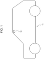
- an electronic device 10 applied to the imaging apparatus according to the first embodiment is, for example, mounted on a mobile body 11.
- the mobile body 11 may include, for example, vehicles, marine vessels, aircrafts, and the like.
- Vehicles may include, for example, automobiles, industrial vehicles, railway vehicles, living vehicles, fixed-wing aircrafts that travel on runways, and the like.
- Automobiles may include, for example, passenger cars, trucks, buses, bicycles, trolley buses, and the like.
- Industrial vehicles may include, for example, industrial vehicles for agriculture and construction, and the like.
- Industrial vehicles may include, for example, forklifts, golf carts, and the like.
- Industrial vehicles for agriculture may include, for example, tractors, cultivators, transplanters, binders, combine harvesters, lawnmowers, and the like.
- Industrial vehicles for construction may include, for example, bulldozers, scrapers, power shovels, crane trucks, dump trucks, road rollers, and the like.
- Vehicles may include man-powered vehicles. Classification of vehicles is not limited to the above examples.
- automobiles may include industrial vehicles that can travel on roads. The same vehicles may be included in a plurality of categories.
- Marine vessels may include, for example, jet skis, boats, tankers, and the like.
- Aircrafts may include, for example, fixed-wing aircrafts, rotary-wing aircrafts, and the like.
- the electronic device 10 includes a first substrate 12, a second substrate 13, a first metal plate 14, and a second metal plate 15.
- the electronic device 10 may further include an imaging optical system 16, a first housing 17, and a second housing 18.
- the first substrate 12 has a flat shape.
- the first substrate 12 may have a substantially rectangular shape.
- an imaging element 19 as an electronic component is mounted on the first substrate 12 on a side opposite to a surface facing a flat portion 23, which will be described later.
- the imaging element 19 is, for example, a CCD (Charge Coupled Device) image sensor and a CMOS (Complementary Metal Oxide Semiconductor) image sensor.
- the imaging element 19 images an optical image formed on a light receiving surface and thereby generates an image signal.
- An electronic component 20 is mounted on at least one main surface of the first substrate 12.
- the electronic component 20 drives the imaging element 19 or processes an image signal generated by the imaging element 19.
- the second substrate 13 has a flat shape.
- the second substrate 13 may have a substantially rectangular shape.
- An electronic component 20 is mounted on at least one main surface of the second substrate 13.
- the electronic component 20 drives the imaging element 19 or processes an image signal generated by the imaging element 19.
- a first connector 21 for electrical connection to the second housing 18 may be mounted on one main surface of the second substrate 13.
- the first substrate 12 may be electrically connected to the second substrate 13 by a flexible substrate 22.
- the imaging element 19 of the first substrate 12 and the first connector 21 of the second substrate 13 may be mounted on main surfaces on the same side in a state in which the entirety of the flexible substrate 22 is extended in a flat shape.
- the first substrate 12 and the second substrate 13 are positioned toward a stacking direction with respective main surfaces facing each other.
- the first metal plate 14 includes the flat portion 23 and a first shield portion 24.
- the flat portion 23 has a flat shape.
- the flat portion 23 may have a substantially rectangular shape wider than the first substrate 12 and the second substrate 13. As illustrated in Fig. 2 and Fig. 3 , the flat portion 23 is interposed between the first substrate 12 and the second substrate 13 in the stacking direction in the electronic device 10. In the electronic device 10, a main surface of the flat portion 23 may be substantially parallel to main surfaces of the first substrate 12 and the second substrate 13.
- the flat portion 23 includes an open portion 25 near a side coupled to the first shield portion 24.
- the open portion 25 may have a substantially rectangular shape.
- the open portion 25 is locked with two lock portions 33 of the second metal plate 15 in the electronic device 10.
- the flat portion 23 directly or indirectly abuts the electronic component 20 mounted on the first substrate 12 and the electronic component 20 mounted on the second substrate 13.
- the heat dissipation sheet 27 may be made of, for example, a soft material having shape followability, like filler-containing silicone rubber, and having relatively large thermal conductivity.
- the first shield portion 24 stands, on the side of the main surface of the flat portion 23 facing the first substrate 12, along a portion of the outer edge of the flat portion 23.
- the first shield portion 24 stands along the entirety of one side of the flat portion 23 and portions of two sides at both ends of the one side.
- the first shield portion 24 covers a portion of a side surface of the first substrate 12 in the electronic device 10.
- the first shield portion 24 includes a first fixation portion 26.
- the first shield portion 24 includes the first fixation portion 26 at a substantially center part of a side facing a side coupled to the flat portion 23.
- the first metal plate 14 is fixed by the first fixation portion 26 to a lens barrel 16A that houses the imaging optical system 16.
- engagement is employed for fixation of the first fixation portion 26 to the lens barrel 16A of the imaging optical system 16.
- the fixation is, however, not limited thereto, and welding, bonding with an adhesive, fastening with a screw, and the like may be employed for the fixation.
- the first metal plate 14 is a metal plate, in other words, a metal flat plate having a desired shape such as that illustrated in Fig. 7 and whose predetermined portions are bent.
- Fig. 7 straight lines to be bent on the surface side are indicated by broken lines, and straight lines to be bent on the rear surface side are indicated by one-dot chain lines.
- the first metal plate 14 may be made of, for example, a metal such as copper or the like having large thermal conductivity.
- the second metal plate 15 includes a second shield portion 28.
- the second shield portion 28 has a substantially rectangular cylindrical shape, and one side of a rectangular shape of a section in an axial direction and portions of two sides at both ends of the one side project in a C-shape in the axial direction. That is, the second shield portion 28 includes an all shield portion 30 having a substantially rectangular cylindrical shape, and a part shield portion 29 continuous from the all shield portion 30 in the axial direction and having a rectangular cylindrical shape whose a portion in a circumferential direction is cut out.
- the second metal plate 15 covers the entire circumference of the side surface of the second substrate 13 and the side surface of the first substrate 12 exposed from the first metal plate 14 in the electronic device 10.
- the all shield portion 30 covers the entire circumference of the side surface of the second substrate 13.
- the part shield portion 29 covers the side surface of the first substrate 12 exposed from the first metal plate 14.
- the second shield portion 28 includes a second fixation portion 31 at an end of the part shield portion 29 on the axial direction side. That is, the second shield portion 28 includes the second fixation portion 31 at an edge of the part shield portion 29 on a side opposite to the side continuous with the all shield portion 30.
- the second fixation portion 31 is disposed at, of the three surfaces of the part shield portion 29, a surface between the other two surfaces.
- the second metal plate 15 is fixed by the second fixation portion 31 to the lens barrel 16A housing the imaging optical system 16.
- engagement is employed for fixation of the second fixation portion 31 to the lens barrel 16A of the imaging optical system 16.
- Fixation is, however, not limited thereto, and welding, bonding with an adhesive, fastening with a screw, and the like may be employed for the fixation.
- the all shield portion 30 of the second shield portion 28 has a gap 32 in the circumferential direction.
- the gap 32 is a space between ends of a metal flat plate that are caused to face each other when the flat plate is bent into the second metal plate 15.
- the all shield portion 30 of the second shield portion 28 includes, near the gap 32, the two lock portions 33 adjacent to each other with the gap 32 interposed therebetween.
- the two lock portions 33 are positioned at an end of the all shield portion 30 on the axial direction side. As illustrated in Fig. 2 , the two lock portions 33 are locked with the open portion 25 of the first metal plate 14 in the electronic device 10.
- the second fixation portion 31 and the two lock portions 33 are provided at mutually facing surfaces in the second shield portion 28.
- the first fixation portion 26 of the first metal plate 14 and the second fixation portion 31 of the second metal plate 15 hold, from two directions perpendicular to an optical axis, the lens barrel 16A housing the imaging optical system 16.
- the second metal plate 15 is a metal plate, in other words, a metal flat plate having a desired shape such as that illustrated in Fig. 9 and whose predetermined portions are bent.
- Fig. 9 straight lines to be bent on the surface side are indicated by broken lines, and straight lines to be bent on the rear surface side are indicated by one-dot chain lines.
- the second metal plate 15 may be made of, for example, a metal such as copper or the like having large thermal conductivity.
- the imaging optical system 16 is constituted by an optical element such as a lens.
- the imaging optical system 16 is designed and formed to have predetermined values of optical characteristics such as angle of field, depth of field, and the like.
- the imaging optical system 16 forms an imaged subject image on a light receiving surface of the imaging element 19.
- the first housing 17 may have a rectangular cylindrical section. As illustrated in Fig. 2 and Fig. 3 , the first housing 17 may house the imaging optical system 16 with the optical axis of the imaging optical system 16 substantially coinciding with the axis of the first housing 17 and with the imaging optical system 16 being exposed from one opening.
- the first housing 17 may house the first substrate 12 such that the imaging element 19 is fixed in an orientation determined at a positioned that is determined relative to the imaging optical system 16.
- the first housing 17 may house the second substrate 13, the first metal plate 14, and the second metal plate 15 such that the above configuration is satisfied for the first substrate 12.
- a third metal plate 34 and an imaging-element cover 35 that surround the side surface of the imaging element 19 in the stacking direction are provided between the imaging optical system 16 and the first substrate 12.
- the third metal plate 34 may be made of, for example, a metal such as copper or the like having large thermal conductivity.
- the third metal plate 34 and the imaging-element cover 35 dissipate heat generated by the imaging element 19 to the outside.
- the imaging-element cover 35 may be made of, for example, a soft material having shape followability, like filler-containing silicone rubber, and having relatively large thermal conductivity.
- the second housing 18 may have a shape including a flat part and a quadrangular prism that extends perpendicular to a main surface of the flat part.
- the second housing 18 may include a second connector 36 that can be fitted to the first connector 21.
- the second housing 18 may include a fourth metal plate 37. As illustrated in Fig. 2 and Fig. 3 , the fourth metal plate 37 abuts the second metal plate 15 in the electronic device 10.
- the second housing 18 may be sealed at the flat part to an opening of the first housing 17 on a side opposite to a side that exposes the imaging optical system 16, that is, on the image side of the imaging optical system 16 in the optical axis direction.
- the third metal plate 34 and the imaging-element cover 35 are attached to the image side of the lens barrel 16A housing the imaging optical system 16 in the optical axis direction of the imaging optical system 16.
- the third metal plate 34 is fixed by a third fixation portion 38 included in the third metal plate 34 to the lens barrel 16A of the imaging optical system 16.
- the first substrate 12 is fixed to the image side of the imaging optical system 16 in the optical axis direction with the imaging optical system 16 and the imaging element 19 facing each other.
- the flat portion 23 of the first metal plate 14 is stuck to the first substrate 12.
- the heat dissipation sheet 27 may be used to stick the flat portion 23 of the first metal plate 14 and the first substrate 12 to each other.
- the first shield portion 24 of the first metal plate 14 does not cover, of the first substrate 12, a part where the flexible substrate 22 is provided.
- the first metal plate 14 is fixed by the first fixation portion 26 to the lens barrel 16A.
- the flexible substrate 22 is folded, and the second substrate 13 is stuck to the flat portion 23.
- the heat dissipation sheet 27 may be used to stick the flat portion 23 of the first metal plate 14 and the second substrate 13 to each other.
- the second metal plate 15 is attached from the side of the first connector 21 in the optical axis direction of the imaging optical system 16 to cover the circumference of the second substrate 13.
- the two lock portions 33 of the second metal plate 15 are locked with the open portion 25 of the first metal plate 14.
- the second metal plate 15 is fixed by the second fixation portion 31 to the lens barrel 16A of the imaging optical system 16.
- an internal structure body 39 of the electronic device 10 is configured.
- the second substrate 13 is connected to the second housing 18 by the first connector 21 being fitted to the second connector 36. Consequently, the fourth metal plate 37 abuts the second metal plate 15.
- the first housing 17 is placed over the second housing 18 to cover the internal structure body 39. That is, the first housing 17 is placed over the second housing 18 to cover the imaging optical system 16, the first substrate 12, the second substrate 13, the first metal plate 14, and the second metal plate 15.
- the first housing 17 is fixed to the second housing 18 in a state in which the first housing 17 is placed over the internal structure body 39, and the electronic device 10 is thereby manufactured. For example, welding, bonding with an adhesive, fastening with a screw, and the like are employed for fixation of the first housing 17 and the second housing 18.
- the electronic device 10 includes the flat portion 23 that is interposed between the first substrate 12 and the second substrate 13 and that indirectly abuts the imaging element 19 mounted on the first substrate 12 and the electronic component 20 mounted on the second substrate 13.
- the imaging element 19 mounted on the first substrate 12 and the electronic component 20 mounted on the second substrate 13, which are heat sources, are close to the flat portion 23, which generally has thermal conductivity higher than that of the heat dissipation sheet 27.
- heat dissipation properties are improved compared with a configuration in which only the heat dissipation sheet 27 is interposed.
- the first shield portion 24 and the second shield portion 28 cover the entire circumference of the side surface of the first substrate 12.
- the electronic device 10 can have shielding properties with respect to radiation noise of the electronic component 20 mounted on the first substrate 12.
- the second shield portion 28 covers the entire circumference of the side surface of the second substrate 13. With such a configuration, the electronic device 10 can have shielding properties with respect to radiation noise of the electronic component 20 mounted on the second substrate 13.
- the first metal plate 14 includes the flat portion 23 and the first shield portion 24.
- the second metal plate 15 includes the second shield portion 28.
- the flat portion 23 and the first shield portion 24 having the above configurations and the second shield portion 28 having the above configuration can be manufactured in a simple configuration without being subjected to steps of welding and the like.
- the electronic device 10 according to the first embodiment can further improve heat dissipation properties with a simple configuration while having shielding properties with respect to radiation noise.
- the first metal plate 14 and the second metal plate 15 abut each other directly or indirectly.
- the electronic device 10 can improve thermal conduction between the first metal plate 14 and the second metal plate 15 compared with a configuration in which the first metal plate 14 and the second metal plate 15 are separated from each other. Therefore, the electronic device 10 can further improve heat dissipation properties by causing heat generated by a component that directly or indirectly abuts only one of the first metal plate 14 and the second metal plate 15 to be conducted also to the other metal plate.
- the electronic device 10 can cause heat of the other metal plate to be conducted to the thermal conductor in the above configuration.
- the first shield portion 24 of the first metal plate 14 covers a portion of the side surface of the first substrate 12, and the second shield portion 28 of the second metal plate 15 covers the entire circumference of the second substrate 13 and a portion of the side surface of the first substrate 12 exposed from the first shield portion 24.
- the electronic device 10 can have shielding properties with respect to radiation noise of the electronic component 20 mounted on the first substrate 12 and the electronic component 20 mounted on the second substrate 13 while enabling the first substrate 12 and the second substrate 13 to be easily stuck to the first metal plate 14, even in a configuration in which the first substrate 12 and the second substrate 13 are connected to each other by a wire or the like, such as the flexible substrate 22, extending from the side surface of the first substrate 12.
- the second metal plate 15 includes the lock portions 33, and the first metal plate 14 and the second metal plate 15 directly abut each other at the lock portions 33.
- the electronic device 10 can increase thermal conduction between the first metal plate 14 and the second metal plate 15 and can connect the first metal plate 14 and the second metal plate 15 to each other stably.
- the second metal plate 15 includes, at the second shield portion 28, the two lock portions 33 adjacent to each other with the gap 32 interposed therebetween.
- the electronic device 10 can give spring properties to the lock portions 33 and can enable the lock portions 33 of the second metal plate 15 to be easily inserted into and fixed to the open portion 25 of the first metal plate 14.
- the electronic device 10 can reduce degradation of the shielding properties by suppressing widening of the gap 32 by the open portion 25 holding the two lock portions 33 adjacent to each other with the gap 32 interposed therebetween.
- the flexible substrate 22 that connects the first substrate 12 and the second substrate 13 to each other is covered by the second shield portion 28.
- the electronic device 10 can suppress degradation of shielding properties with respect to radiation noise of the electronic component 20 mounted on the first substrate 12 and the electronic component 20 mounted on the second substrate 13 while using the flexible substrate 22 that contributes to easy manufacture and a reduction in manufacturing costs.
- the electronic device 10 according to a second embodiment of the present disclosure will be described.
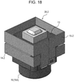
- the configuration of the internal structure body of the electronic device 10 differs from that in the first embodiment. More specifically, as illustrated in Fig. 18 , in an internal structure body 39-2 according to the second embodiment, the shapes of a first metal plate 14-2 and a second metal plate 15-2 differ from the shapes of the first metal plate 14 and the second metal plate 15 of the internal structure body 39 according to the first embodiment, illustrated in Fig. 17 .
- features that differ from those in the first embodiment will be mainly described. Parts having the same configurations as those in the first embodiment are given the same signs.
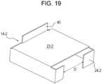
- the first metal plate 14-2 With reference to Fig. 19 and Fig. 20 , the first metal plate 14-2 will be described. As illustrated in Fig. 19 , the first metal plate 14-2 includes a flat portion 23-2 and a first shield portion 24-2.
- the flat portion 23-2 differs from the flat portion 23 according to the first embodiment in that the main surface thereof does not include the open portion 25.
- the structure of the flat portion 23-2 other than the feature of not including the open portion 25 may be the same as the structure of the flat portion 23 according to the first embodiment.
- the relationship of the flat portion 23-2 with the first substrate 12 and the second substrate 13 may be the same as that in the first embodiment.
- the first shield portion 24-2 stands along a portion of the outer edge of the flat portion 23-2.
- the first shield portion 24-2 is coupled at all of two mutually facing sides of the flat portion 23-2 to the flat portion 23-2.
- the first shield portion 24-2 stands along the two sides and portions of the other two sides at both ends of the two sides.
- the first shield portion 24-2 stands at both end portions of the one side with a gap of a distance D.
- the distance D may be longer than the width of the flexible substrate 22.
- the flat portion 23-2 includes a standing portion 40 standing along a portion of the outer edge of the flat portion 23-2 in a direction opposite to the direction in which the first shield portion 24-2 stands.
- the main surface of the standing portion 40 faces a surface of the first shield portion 24-2 having the gap of the distance D.
- the standing portion 40 is coupled to the first shield portion 24-2 at a side of the outer edge of the flat portion 23-2. The side differs from the sides to which the first shield portion 24-2 is coupled.
- Fig. 20 illustrates the first metal plate 14-2 as viewed from an opposite side in a direction perpendicular to the flat portion 23-2 in contrast to Fig. 19 .
- a contact portion 41 extending on a side opposite to the side of the standing portion 40 is present.
- the contact portion 41 is in contact with the third metal plate 34.
- the first metal plate 14-2 is a metal plate, in other words, a metal flat plate having a desired shape such as that illustrated in Fig. 21 and whose predetermined portions are bent.
- Fig. 21 straight lines to be bent on the surface side are indicated by broken lines, and straight lines to be bent on the rear surface side are indicated by one-dot chain lines.
- the first metal plate 14-2 may be made of, for example, a metal such as copper or the like having large thermal conductivity.
- the second metal plate 15-2 includes a second shield portion 28-2.
- the second shield portion 28-2 has a substantially rectangular cylindrical shape and has a section having a rectangular shape in the axial direction. Portions of mutually facing two sides of the rectangular shape project in the axial direction. That is, the second shield portion 28-2 includes an all shield portion 30-2 having a substantially rectangular cylindrical shape, and two part shield portions 29-2 projecting from a portion of each of mutually facing two sides of the rectangular shape of the section in the axial direction and continuous from the all shield portion 30-2 in the axial direction.
- the main surfaces of the two part shield portions 29-2 face each other.
- the widths of the main surfaces of the two part shield portions 29-2 that is, the lengths thereof in a direction perpendicular to the axial direction may differ from each other.
- the second metal plate 15-2 covers the entire circumference of the side surface of the second substrate 13 and a portion of the side surface of the first substrate 12 exposed from the first metal plate 14-2.
- the all shield portion 30-2 covers the entire circumference of the side surface of the second substrate 13, and the part shield portions 29-2 covers a portion of the side surface of the first substrate 12 exposed from the first metal plate 14.
- the two part shield portions 29-2 of the second shield portion 28-2 each include the second fixation portion 31 at an end on a side not continuous with the all shield portion 30-2. Consequently, when the second metal plate 15-2 is attached to the electronic device 10, the two second fixation portions 31 hold the lens barrel 16A housing the imaging optical system 16 from two directions perpendicular to the optical axis.
- the second shield portion 28-2 includes the gap 32 extending over one of the part shield portions 29-2 and the all shield portion 30-2 in the circumferential direction.
- the gap 32 is substantially parallel to the axial direction.
- the gap 32 is a space between ends of a metal flat plate that are caused to face each other when the flat plate is bent into the second metal plate 15-2.
- the second fixation portion 31 at one of the part shield portions 29-2 is positioned near the gap 32.
- a contact portion 42 adjacent, at the one of the part shield portions 29-2, to the second fixation portion 31 with the gap 32 therebetween is in contact with the third metal plate 34 in the electronic device 10.
- the second metal plate 15-2 is a metal plate, in other words, a metal flat plate having a desired shape such as that illustrated in Fig. 23 and whose predetermined portions are bent.
- Fig. 23 straight lines to be bent on the surface side are indicated by broken lines, and straight lines to be bent on the rear surface side are indicated by one-dot chain lines.
- the second metal plate 15-2 may be made of, for example, a metal such as copper or the like having large thermal conductivity.
- the first substrate 12 is attached to the lens barrel 16A housing the imaging optical system 16 via the third metal plate 34 and the imaging-element cover 35.
- the flat portion 23-2 of the first metal plate 14-2 is stuck to the first substrate 12.
- the heat dissipation sheet 27 may be used to stick the flat portion 23-2 of the first metal plate 14-2 and the first substrate 12 to each other.
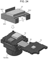
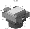
- the first metal plate 14-2 is stuck to the first substrate 12 to enable the flexible substrate 22 of the first substrate 12 to pass through the gap of the distance D included in the first shield portion 24-2. Consequently, as illustrated in Fig. 25 , the contact portion 41 of the first metal plate 14-2 is in contact with the third metal plate 34.
- Fig. 25 illustrates a state in which the first metal plate 14-2 is stuck to the first substrate 12, the state being rotated around the axial direction of the lens barrel 16A by 180 degrees from that in Fig. 19 . In Fig. 25 , illustration of a portion of the flexible substrate 22 and the second substrate 13 is omitted.
- the flexible substrate 22 is folded, and the second substrate 13 is stuck to the flat portion 23-2.
- the heat dissipation sheet 27 may be used to stick the flat portion 23-2 of the first metal plate 14-2 and the second substrate 13 to each other.
- the second metal plate 15-2 is attached from the side of the first connector 21 in the optical axis direction of the imaging optical system 16 to cover the circumference of the second substrate 13.
- the second metal plate 15-2 is fixed by the two second fixation portions 31 to the lens barrel 16A housing the imaging optical system 16. Consequently, the contact portion 42 of the second metal plate 15-2 is in contact with the third metal plate 34.
- the first metal plate 14-2 and the second metal plate 15-2 abut each other indirectly via the third metal plate 34.
- the internal structure body 39-2 of the electronic device 10 is configured as illustrated in Fig. 18 .
- the flat portion 23-2 of the first metal plate 14-2 is not provided with an open portion for locking, as with the first embodiment, the first metal plate 14-2 and the second metal plate 15-2 with each other.
- the electronic device 10 can increase the area of the flat portion 23 that can directly or indirectly abut the imaging element 19 mounted on the first substrate 12 and the electronic component 20 mounted on the second substrate 13, which are heat sources, and can improve heat dissipation properties.
- the first metal plate 14-2 and the second metal plate 15-2 abut each other indirectly via the third metal plate 34.
- the electronic device 10 can reduce heat conduction between the first metal plate 14-2 and the second metal plate 15-2 compared with a configuration in which the first metal plate 14-2 and the second metal plate 15-2 abut each other.
- the electronic device 10 can reduce heat conduction from the other one to the one even when the temperature of the other one is increased.
Landscapes
- Engineering & Computer Science (AREA)
- Physics & Mathematics (AREA)
- General Physics & Mathematics (AREA)
- Multimedia (AREA)
- Signal Processing (AREA)
- Electromagnetism (AREA)
- Microelectronics & Electronic Packaging (AREA)
- Aviation & Aerospace Engineering (AREA)
- Thermal Sciences (AREA)
- Studio Devices (AREA)
- Camera Bodies And Camera Details Or Accessories (AREA)
- Shielding Devices Or Components To Electric Or Magnetic Fields (AREA)
- Cameras Adapted For Combination With Other Photographic Or Optical Apparatuses (AREA)
- Lens Barrels (AREA)
- Cooling Or The Like Of Electrical Apparatus (AREA)
Abstract
Description
- The present application claims priority of
Japanese Patent Application No. 2019-053724, filed on March 20, 2019 - The present disclosure relates to an electronic device, an imaging apparatus, and a mobile body.
- Electronic devices such as onboard cameras are required to be downsized and to perform various processing at a high speed. As a result of a circuit board being multilayered and highly-integrated for downsizing, radiation noise and the amount of heat generated by an electronic device of the circuit board are increased. There is proposed a configuration in which the entirety of the side surface of a circuit board is covered by a shield member and in which the circuit board and a heat conduction member abut each other via a heat conduction member made of a soft material such as silicone gel (refer to PTL 1).
- PTL 1:
Japanese Unexamined Patent Application No. 2011-259101 - To solve the above problems, an electronic device according to a first aspect includes:
- a first substrate and a second substrate on each of which an electronic component is mounted, the first substrate and the second substrate being positioned toward a stacking direction with respective main surfaces facing each other;
- a first metal plate including a flat portion that is interposed between the first substrate and the second substrate and that directly or indirectly abuts the electronic component mounted on the first substrate and the electronic component mounted on the second substrate, and a first shield portion that covers a portion of a side surface of the first substrate; and
- a second metal plate including a second shield portion that covers an entire circumference of a side surface of the second substrate and the side surface of the first substrate exposed from the first metal plate,
- in which the first metal plate and the second metal plate abut each other directly or indirectly.
- An imaging apparatus according to a second aspect includes:
- a first substrate and a second substrate on each of which an electronic component is mounted, the first substrate and the second substrate being positioned toward a stacking direction with respective main surfaces facing each other;
- a first metal plate including a flat portion that is interposed between the first substrate and the second substrate and that directly or indirectly abuts the electronic component mounted on the first substrate and the electronic component mounted on the second substrate, and a first shield portion that covers a portion of a side surface of the first substrate; and
- a second metal plate including a second shield portion that covers an entire circumference of a side surface of the second substrate and the side surface of the first substrate exposed from the first metal plate,
- in which the first metal plate and the second metal plate abut each other directly or indirectly.
- A mobile body according to a third aspect includes an imaging apparatus mounted thereon, the imaging apparatus including:
- a first substrate and a second substrate on each of which an electronic component is mounted, the first substrate and the second substrate being positioned toward a stacking direction with respective main surfaces facing each other;
- a first metal plate including a flat portion that is interposed between the first substrate and the second substrate and that directly or indirectly abuts the electronic component mounted on the first substrate and the electronic component mounted on the second substrate, and a first shield portion that covers a portion of a side surface of the first substrate; and
- a second metal plate including a second shield portion that covers an entire circumference of a side surface of the second substrate and the side surface of the first substrate exposed from the first metal plate,
- in which the first metal plate and the second metal plate abut each other directly or indirectly.
-
- [
Fig. 1] Fig. 1 is an arrangement diagram illustrating a mounting position of an electronic device according to a first embodiment in a mobile body. - [
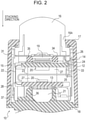
Fig. 2] Fig. 2 is a sectional view illustrating a general configuration of the electronic device inFig. 1 , the sectional view being cut to pass through an optical axis of an imaging optical system and. - [
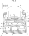
Fig. 3] Fig. 3 is a sectional view in which the electronic device inFig. 1 is rotated around the optical axis by 90° from that in the section inFig. 2 . - [
Fig. 4] Fig. 4 is a front perspective view illustrating appearances of a first substrate and a second substrate inFig. 2 andFig. 3 . - [
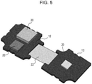
Fig. 5] Fig. 5 is a rear perspective view illustrating appearances of the first substrate and the second substrate inFig. 2 andFig. 3 . - [
Fig. 6] Fig. 6 is a perspective view illustrating an appearance of a first metal plate inFig. 2 andFig. 3 . - [
Fig. 7] Fig. 7 is a development plan view of the first metal plate inFig. 6 . - [
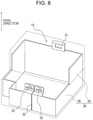
Fig. 8] Fig. 8 is a perspective view illustrating an appearance of a second metal plate inFig. 2 andFig. 3 . - [
Fig. 9] Fig. 9 is a development plan view of the second metal plate inFig. 8 . - [
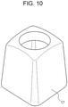
Fig. 10] Fig. 10 is a perspective view illustrating an appearance of a first housing inFig. 2 andFig. 3 . - [
Fig. 11] Fig. 11 is a perspective view illustrating an appearance of a second housing inFig. 2 andFig. 3 . - [
Fig. 12] Fig. 12 illustrates a method of manufacturing the electronic device inFig. 2 andFig. 3 and illustrates a step of assembling a third metal plate and an imaging-element cover to an imaging optical system. - [
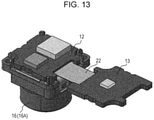
Fig. 13] Fig. 13 illustrates a method of manufacturing the electronic device inFig. 2 andFig. 3 and illustrates a step of assembling a first substrate to an imaging optical system. - [
Fig. 14] Fig. 14 illustrates a method of manufacturing the electronic device inFig. 2 andFig. 3 and illustrates another step of assembling a first substrate and a second substrate to a first metal plate. - [
Fig. 15] Fig. 15 illustrates a method of manufacturing the electronic device inFig. 2 andFig. 3 and illustrates yet another step of assembling a first substrate and a second substrate to a first metal plate. - [
Fig. 16] Fig. 16 illustrates a method of manufacturing the electronic device inFig. 2 andFig. 3 and illustrates a step of assembling a second metal plate to a first metal plate. - [
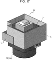
Fig. 17] Fig. 17 is a perspective view illustrating an appearance of an internal structure body of the electronic device inFig. 2 andFig. 3 . - [
Fig. 18] Fig. 18 is a perspective view illustrating an appearance of another internal structure body of an electronic device according to a second embodiment. - [
Fig. 19] Fig. 19 is a perspective view illustrating an appearance of a first metal plate included in the internal structure body inFig. 18 . - [
Fig. 20] Fig. 20 is a perspective view illustrating an appearance of the first metal plate inFig. 19 from an angle that differs from the angle inFig. 19 . - [
Fig. 21] Fig. 21 is a development plan view of the first metal plate inFig. 19 . - [
Fig. 22] Fig. 22 is a perspective view illustrating an appearance of a second metal plate included in the internal structure body inFig. 18 . - [
Fig. 23] Fig. 23 is a development plan view of the second metal plate inFig. 22 . - [
Fig. 24] Fig. 24 illustrates a method of manufacturing the internal structure body inFig. 18 and illustrates a step of assembling a first metal plate to a first substrate. - [
Fig. 25] Fig. 25 illustrates a state in which the first metal plate inFig. 24 is assembled to a first substrate. - [
Fig. 26] Fig. 26 illustrates a method of manufacturing the internal structure body inFig. 18 and illustrates a step of assembling a second substrate to an imaging optical system. - Electronic devices are demanded to further improve heat dissipation properties with a simple configuration while having shielding properties with respect to radiation noise. An object of the present disclosure is to provide an electronic device that further improves heat dissipation properties with a simple configuration while having shielding properties with respect to radiation noise, an imaging apparatus, and a mobile body.
- Hereinafter, an electronic device, an imaging apparatus, and a mobile body according to a first embodiment of the present disclosure will be described with reference to the drawings.
- Specifically, the electronic device according to the first embodiment is, for example, an imaging apparatus. As illustrated in
Fig. 1 , anelectronic device 10 applied to the imaging apparatus according to the first embodiment is, for example, mounted on amobile body 11. - The
mobile body 11 may include, for example, vehicles, marine vessels, aircrafts, and the like. Vehicles may include, for example, automobiles, industrial vehicles, railway vehicles, living vehicles, fixed-wing aircrafts that travel on runways, and the like. Automobiles may include, for example, passenger cars, trucks, buses, bicycles, trolley buses, and the like. Industrial vehicles may include, for example, industrial vehicles for agriculture and construction, and the like. Industrial vehicles may include, for example, forklifts, golf carts, and the like. Industrial vehicles for agriculture may include, for example, tractors, cultivators, transplanters, binders, combine harvesters, lawnmowers, and the like. Industrial vehicles for construction may include, for example, bulldozers, scrapers, power shovels, crane trucks, dump trucks, road rollers, and the like. Vehicles may include man-powered vehicles. Classification of vehicles is not limited to the above examples. For example, automobiles may include industrial vehicles that can travel on roads. The same vehicles may be included in a plurality of categories. Marine vessels may include, for example, jet skis, boats, tankers, and the like. Aircrafts may include, for example, fixed-wing aircrafts, rotary-wing aircrafts, and the like. - As illustrated in
Fig. 2 andFig. 3 , theelectronic device 10 includes afirst substrate 12, asecond substrate 13, afirst metal plate 14, and asecond metal plate 15. Theelectronic device 10 may further include an imagingoptical system 16, afirst housing 17, and asecond housing 18. - As illustrated in
Fig. 4 andFig. 5 , thefirst substrate 12 has a flat shape. Thefirst substrate 12 may have a substantially rectangular shape. As illustrated inFig. 2 andFig. 3 , animaging element 19 as an electronic component is mounted on thefirst substrate 12 on a side opposite to a surface facing aflat portion 23, which will be described later. Theimaging element 19 is, for example, a CCD (Charge Coupled Device) image sensor and a CMOS (Complementary Metal Oxide Semiconductor) image sensor. Theimaging element 19 images an optical image formed on a light receiving surface and thereby generates an image signal. Anelectronic component 20 is mounted on at least one main surface of thefirst substrate 12. Theelectronic component 20 drives theimaging element 19 or processes an image signal generated by theimaging element 19. - As illustrated in
Fig. 4 andFig. 5 , thesecond substrate 13 has a flat shape. Thesecond substrate 13 may have a substantially rectangular shape. Anelectronic component 20 is mounted on at least one main surface of thesecond substrate 13. Theelectronic component 20 drives theimaging element 19 or processes an image signal generated by theimaging element 19. Afirst connector 21 for electrical connection to thesecond housing 18 may be mounted on one main surface of thesecond substrate 13. - The
first substrate 12 may be electrically connected to thesecond substrate 13 by aflexible substrate 22. As illustrated inFig. 4 , theimaging element 19 of thefirst substrate 12 and thefirst connector 21 of thesecond substrate 13 may be mounted on main surfaces on the same side in a state in which the entirety of theflexible substrate 22 is extended in a flat shape. - As illustrated in
Fig. 2 andFig. 3 , in theelectronic device 10, thefirst substrate 12 and thesecond substrate 13 are positioned toward a stacking direction with respective main surfaces facing each other. - As illustrated in
Fig. 6 , thefirst metal plate 14 includes theflat portion 23 and afirst shield portion 24. - The
flat portion 23 has a flat shape. Theflat portion 23 may have a substantially rectangular shape wider than thefirst substrate 12 and thesecond substrate 13. As illustrated inFig. 2 andFig. 3 , theflat portion 23 is interposed between thefirst substrate 12 and thesecond substrate 13 in the stacking direction in theelectronic device 10. In theelectronic device 10, a main surface of theflat portion 23 may be substantially parallel to main surfaces of thefirst substrate 12 and thesecond substrate 13. - As illustrated in
Fig. 6 , theflat portion 23 includes anopen portion 25 near a side coupled to thefirst shield portion 24. Theopen portion 25 may have a substantially rectangular shape. As illustrated inFig. 2 , theopen portion 25 is locked with twolock portions 33 of thesecond metal plate 15 in theelectronic device 10. - In the
electronic device 10, theflat portion 23 directly or indirectly abuts theelectronic component 20 mounted on thefirst substrate 12 and theelectronic component 20 mounted on thesecond substrate 13. In theelectronic device 10, theflat portion 23, for example, indirectly abuts theimaging element 19 as an electronic component via aheat dissipation sheet 27 and thefirst substrate 12. In theelectronic device 10, theflat portion 23, for example, indirectly abuts theelectronic component 20 mounted on thesecond substrate 13 via theheat dissipation sheet 27. Theheat dissipation sheet 27 may be made of, for example, a soft material having shape followability, like filler-containing silicone rubber, and having relatively large thermal conductivity. - As illustrated in
Fig. 6 , thefirst shield portion 24 stands, on the side of the main surface of theflat portion 23 facing thefirst substrate 12, along a portion of the outer edge of theflat portion 23. For example, thefirst shield portion 24 stands along the entirety of one side of theflat portion 23 and portions of two sides at both ends of the one side. As illustrated inFig. 2 andFig. 3 , thefirst shield portion 24 covers a portion of a side surface of thefirst substrate 12 in theelectronic device 10. - As illustrated in
Fig. 6 , thefirst shield portion 24 includes afirst fixation portion 26. In the present embodiment, thefirst shield portion 24 includes thefirst fixation portion 26 at a substantially center part of a side facing a side coupled to theflat portion 23. As illustrated inFig. 2 andFig. 3 , thefirst metal plate 14 is fixed by thefirst fixation portion 26 to alens barrel 16A that houses the imagingoptical system 16. For example, engagement is employed for fixation of thefirst fixation portion 26 to thelens barrel 16A of the imagingoptical system 16. The fixation is, however, not limited thereto, and welding, bonding with an adhesive, fastening with a screw, and the like may be employed for the fixation. - The
first metal plate 14 is a metal plate, in other words, a metal flat plate having a desired shape such as that illustrated inFig. 7 and whose predetermined portions are bent. InFig. 7 , straight lines to be bent on the surface side are indicated by broken lines, and straight lines to be bent on the rear surface side are indicated by one-dot chain lines. When the bent portions of thefirst metal plate 14 are unbent into a flat shape, all of parts of thefirst metal plate 14 are thus separated from each other without interfering with each other. Thefirst metal plate 14 may be made of, for example, a metal such as copper or the like having large thermal conductivity. - As illustrated in
Fig. 8 , thesecond metal plate 15 includes asecond shield portion 28. - The
second shield portion 28 has a substantially rectangular cylindrical shape, and one side of a rectangular shape of a section in an axial direction and portions of two sides at both ends of the one side project in a C-shape in the axial direction. That is, thesecond shield portion 28 includes an allshield portion 30 having a substantially rectangular cylindrical shape, and apart shield portion 29 continuous from the allshield portion 30 in the axial direction and having a rectangular cylindrical shape whose a portion in a circumferential direction is cut out. As illustrated inFig. 2 andFig. 3 , thesecond metal plate 15 covers the entire circumference of the side surface of thesecond substrate 13 and the side surface of thefirst substrate 12 exposed from thefirst metal plate 14 in theelectronic device 10. In this configuration, the allshield portion 30 covers the entire circumference of the side surface of thesecond substrate 13. Thepart shield portion 29 covers the side surface of thefirst substrate 12 exposed from thefirst metal plate 14. - As illustrated in
Fig. 8 , thesecond shield portion 28 includes asecond fixation portion 31 at an end of thepart shield portion 29 on the axial direction side. That is, thesecond shield portion 28 includes thesecond fixation portion 31 at an edge of thepart shield portion 29 on a side opposite to the side continuous with the allshield portion 30. In the present embodiment, thesecond fixation portion 31 is disposed at, of the three surfaces of thepart shield portion 29, a surface between the other two surfaces. As illustrated inFig. 2 , thesecond metal plate 15 is fixed by thesecond fixation portion 31 to thelens barrel 16A housing the imagingoptical system 16. For example, engagement is employed for fixation of thesecond fixation portion 31 to thelens barrel 16A of the imagingoptical system 16. Fixation is, however, not limited thereto, and welding, bonding with an adhesive, fastening with a screw, and the like may be employed for the fixation. - As illustrated in
Fig. 8 , the allshield portion 30 of thesecond shield portion 28 has agap 32 in the circumferential direction. Thegap 32 is a space between ends of a metal flat plate that are caused to face each other when the flat plate is bent into thesecond metal plate 15. The allshield portion 30 of thesecond shield portion 28 includes, near thegap 32, the twolock portions 33 adjacent to each other with thegap 32 interposed therebetween. The twolock portions 33 are positioned at an end of the allshield portion 30 on the axial direction side. As illustrated inFig. 2 , the twolock portions 33 are locked with theopen portion 25 of thefirst metal plate 14 in theelectronic device 10. - As illustrated in
Fig. 8 , thesecond fixation portion 31 and the twolock portions 33 are provided at mutually facing surfaces in thesecond shield portion 28. Thus, as illustrated inFig. 2 , when thefirst metal plate 14 and thesecond metal plate 15 are attached to theelectronic device 10, thefirst fixation portion 26 of thefirst metal plate 14 and thesecond fixation portion 31 of thesecond metal plate 15 hold, from two directions perpendicular to an optical axis, thelens barrel 16A housing the imagingoptical system 16. - The
second metal plate 15 is a metal plate, in other words, a metal flat plate having a desired shape such as that illustrated inFig. 9 and whose predetermined portions are bent. InFig. 9 , straight lines to be bent on the surface side are indicated by broken lines, and straight lines to be bent on the rear surface side are indicated by one-dot chain lines. When the bent portions of thesecond metal plate 15 are unbent into a flat shape, all of parts of thesecond metal plate 15 are thus separated from each other without interfering with each other. Thesecond metal plate 15 may be made of, for example, a metal such as copper or the like having large thermal conductivity. - The imaging
optical system 16 is constituted by an optical element such as a lens. The imagingoptical system 16 is designed and formed to have predetermined values of optical characteristics such as angle of field, depth of field, and the like. The imagingoptical system 16 forms an imaged subject image on a light receiving surface of theimaging element 19. - As illustrated in
Fig. 10 , thefirst housing 17 may have a rectangular cylindrical section. As illustrated inFig. 2 andFig. 3 , thefirst housing 17 may house the imagingoptical system 16 with the optical axis of the imagingoptical system 16 substantially coinciding with the axis of thefirst housing 17 and with the imagingoptical system 16 being exposed from one opening. Thefirst housing 17 may house thefirst substrate 12 such that theimaging element 19 is fixed in an orientation determined at a positioned that is determined relative to the imagingoptical system 16. Thefirst housing 17 may house thesecond substrate 13, thefirst metal plate 14, and thesecond metal plate 15 such that the above configuration is satisfied for thefirst substrate 12. - As illustrated in
Fig. 2 andFig. 3 , athird metal plate 34 and an imaging-element cover 35 that surround the side surface of theimaging element 19 in the stacking direction are provided between the imagingoptical system 16 and thefirst substrate 12. Thethird metal plate 34 may be made of, for example, a metal such as copper or the like having large thermal conductivity. Thethird metal plate 34 and the imaging-element cover 35 dissipate heat generated by theimaging element 19 to the outside. The imaging-element cover 35 may be made of, for example, a soft material having shape followability, like filler-containing silicone rubber, and having relatively large thermal conductivity. - As illustrated in
Fig. 11 , thesecond housing 18 may have a shape including a flat part and a quadrangular prism that extends perpendicular to a main surface of the flat part. Thesecond housing 18 may include asecond connector 36 that can be fitted to thefirst connector 21. Thesecond housing 18 may include afourth metal plate 37. As illustrated inFig. 2 andFig. 3 , thefourth metal plate 37 abuts thesecond metal plate 15 in theelectronic device 10. Thesecond housing 18 may be sealed at the flat part to an opening of thefirst housing 17 on a side opposite to a side that exposes the imagingoptical system 16, that is, on the image side of the imagingoptical system 16 in the optical axis direction. - Next, a method of manufacturing the
electronic device 10 will be described below. - As illustrated in
Fig. 12 , thethird metal plate 34 and the imaging-element cover 35 are attached to the image side of thelens barrel 16A housing the imagingoptical system 16 in the optical axis direction of the imagingoptical system 16. Thethird metal plate 34 is fixed by athird fixation portion 38 included in thethird metal plate 34 to thelens barrel 16A of the imagingoptical system 16. - As illustrated in
Fig. 13 , thefirst substrate 12 is fixed to the image side of the imagingoptical system 16 in the optical axis direction with the imagingoptical system 16 and theimaging element 19 facing each other. - As illustrated in
Fig. 14 , theflat portion 23 of thefirst metal plate 14 is stuck to thefirst substrate 12. Theheat dissipation sheet 27 may be used to stick theflat portion 23 of thefirst metal plate 14 and thefirst substrate 12 to each other. Thefirst shield portion 24 of thefirst metal plate 14 does not cover, of thefirst substrate 12, a part where theflexible substrate 22 is provided. Thefirst metal plate 14 is fixed by thefirst fixation portion 26 to thelens barrel 16A. - As illustrated in
Fig. 15 , theflexible substrate 22 is folded, and thesecond substrate 13 is stuck to theflat portion 23. Theheat dissipation sheet 27 may be used to stick theflat portion 23 of thefirst metal plate 14 and thesecond substrate 13 to each other. - As illustrated in
Fig. 16 , thesecond metal plate 15 is attached from the side of thefirst connector 21 in the optical axis direction of the imagingoptical system 16 to cover the circumference of thesecond substrate 13. The twolock portions 33 of thesecond metal plate 15 are locked with theopen portion 25 of thefirst metal plate 14. Thesecond metal plate 15 is fixed by thesecond fixation portion 31 to thelens barrel 16A of the imagingoptical system 16. Thus, as illustrated inFig. 17 , aninternal structure body 39 of theelectronic device 10 is configured. - As illustrated in
Fig. 2 andFig. 3 , thesecond substrate 13 is connected to thesecond housing 18 by thefirst connector 21 being fitted to thesecond connector 36. Consequently, thefourth metal plate 37 abuts thesecond metal plate 15. Thereafter, thefirst housing 17 is placed over thesecond housing 18 to cover theinternal structure body 39. That is, thefirst housing 17 is placed over thesecond housing 18 to cover the imagingoptical system 16, thefirst substrate 12, thesecond substrate 13, thefirst metal plate 14, and thesecond metal plate 15. Thefirst housing 17 is fixed to thesecond housing 18 in a state in which thefirst housing 17 is placed over theinternal structure body 39, and theelectronic device 10 is thereby manufactured. For example, welding, bonding with an adhesive, fastening with a screw, and the like are employed for fixation of thefirst housing 17 and thesecond housing 18. - The
electronic device 10 according to the first embodiment with the above configuration includes theflat portion 23 that is interposed between thefirst substrate 12 and thesecond substrate 13 and that indirectly abuts theimaging element 19 mounted on thefirst substrate 12 and theelectronic component 20 mounted on thesecond substrate 13. In theelectronic device 10 with such a configuration, theimaging element 19 mounted on thefirst substrate 12 and theelectronic component 20 mounted on thesecond substrate 13, which are heat sources, are close to theflat portion 23, which generally has thermal conductivity higher than that of theheat dissipation sheet 27. Thus, heat dissipation properties are improved compared with a configuration in which only theheat dissipation sheet 27 is interposed. - In the
electronic device 10 according to the first embodiment, thefirst shield portion 24 and thesecond shield portion 28 cover the entire circumference of the side surface of thefirst substrate 12. With such a configuration, theelectronic device 10 can have shielding properties with respect to radiation noise of theelectronic component 20 mounted on thefirst substrate 12. In theelectronic device 10 according to the first embodiment, thesecond shield portion 28 covers the entire circumference of the side surface of thesecond substrate 13. With such a configuration, theelectronic device 10 can have shielding properties with respect to radiation noise of theelectronic component 20 mounted on thesecond substrate 13. - In the
electronic device 10 according to the first embodiment, thefirst metal plate 14 includes theflat portion 23 and thefirst shield portion 24. In theelectronic device 10, thesecond metal plate 15 includes thesecond shield portion 28. In theelectronic device 10 with such a configuration, theflat portion 23 and thefirst shield portion 24 having the above configurations and thesecond shield portion 28 having the above configuration can be manufactured in a simple configuration without being subjected to steps of welding and the like. - Therefore, as described above, the
electronic device 10 according to the first embodiment can further improve heat dissipation properties with a simple configuration while having shielding properties with respect to radiation noise. - In the
electronic device 10 according to the first embodiment, thefirst metal plate 14 and thesecond metal plate 15 abut each other directly or indirectly. With such a configuration, theelectronic device 10 can improve thermal conduction between thefirst metal plate 14 and thesecond metal plate 15 compared with a configuration in which thefirst metal plate 14 and thesecond metal plate 15 are separated from each other. Therefore, theelectronic device 10 can further improve heat dissipation properties by causing heat generated by a component that directly or indirectly abuts only one of thefirst metal plate 14 and thesecond metal plate 15 to be conducted also to the other metal plate. For example, in a configuration in which only one of thefirst metal plate 14 and thesecond metal plate 15 abuts a thermal conductor, such as thefourth metal plate 37, for conducting heat inside theelectronic device 10 to the outside, theelectronic device 10 can cause heat of the other metal plate to be conducted to the thermal conductor in the above configuration. - In the
electronic device 10 according to the first embodiment, thefirst shield portion 24 of thefirst metal plate 14 covers a portion of the side surface of thefirst substrate 12, and thesecond shield portion 28 of thesecond metal plate 15 covers the entire circumference of thesecond substrate 13 and a portion of the side surface of thefirst substrate 12 exposed from thefirst shield portion 24. With such a configuration, theelectronic device 10 can have shielding properties with respect to radiation noise of theelectronic component 20 mounted on thefirst substrate 12 and theelectronic component 20 mounted on thesecond substrate 13 while enabling thefirst substrate 12 and thesecond substrate 13 to be easily stuck to thefirst metal plate 14, even in a configuration in which thefirst substrate 12 and thesecond substrate 13 are connected to each other by a wire or the like, such as theflexible substrate 22, extending from the side surface of thefirst substrate 12. - In the
electronic device 10 according to the first embodiment, thesecond metal plate 15 includes thelock portions 33, and thefirst metal plate 14 and thesecond metal plate 15 directly abut each other at thelock portions 33. With such a configuration, theelectronic device 10 can increase thermal conduction between thefirst metal plate 14 and thesecond metal plate 15 and can connect thefirst metal plate 14 and thesecond metal plate 15 to each other stably. - In the
electronic device 10 according to the first embodiment, thesecond metal plate 15 includes, at thesecond shield portion 28, the twolock portions 33 adjacent to each other with thegap 32 interposed therebetween. With such a configuration, theelectronic device 10 can give spring properties to thelock portions 33 and can enable thelock portions 33 of thesecond metal plate 15 to be easily inserted into and fixed to theopen portion 25 of thefirst metal plate 14. In addition, theelectronic device 10 can reduce degradation of the shielding properties by suppressing widening of thegap 32 by theopen portion 25 holding the twolock portions 33 adjacent to each other with thegap 32 interposed therebetween. - In the
electronic device 10 according to the first embodiment, theflexible substrate 22 that connects thefirst substrate 12 and thesecond substrate 13 to each other is covered by thesecond shield portion 28. With such a configuration, theelectronic device 10 can suppress degradation of shielding properties with respect to radiation noise of theelectronic component 20 mounted on thefirst substrate 12 and theelectronic component 20 mounted on thesecond substrate 13 while using theflexible substrate 22 that contributes to easy manufacture and a reduction in manufacturing costs. - Next, with reference to
Fig. 18 to Fig. 26 , theelectronic device 10 according to a second embodiment of the present disclosure will be described. In the second embodiment, the configuration of the internal structure body of theelectronic device 10 differs from that in the first embodiment. More specifically, as illustrated inFig. 18 , in an internal structure body 39-2 according to the second embodiment, the shapes of a first metal plate 14-2 and a second metal plate 15-2 differ from the shapes of thefirst metal plate 14 and thesecond metal plate 15 of theinternal structure body 39 according to the first embodiment, illustrated inFig. 17 . Regarding the second embodiment, features that differ from those in the first embodiment will be mainly described. Parts having the same configurations as those in the first embodiment are given the same signs. - With reference to
Fig. 19 andFig. 20 , the first metal plate 14-2 will be described. As illustrated inFig. 19 , the first metal plate 14-2 includes a flat portion 23-2 and a first shield portion 24-2. - The flat portion 23-2 differs from the
flat portion 23 according to the first embodiment in that the main surface thereof does not include theopen portion 25. The structure of the flat portion 23-2 other than the feature of not including theopen portion 25 may be the same as the structure of theflat portion 23 according to the first embodiment. The relationship of the flat portion 23-2 with thefirst substrate 12 and thesecond substrate 13 may be the same as that in the first embodiment. - The first shield portion 24-2 stands along a portion of the outer edge of the flat portion 23-2. For example, the first shield portion 24-2 is coupled at all of two mutually facing sides of the flat portion 23-2 to the flat portion 23-2. The first shield portion 24-2 stands along the two sides and portions of the other two sides at both ends of the two sides. At one side of two sides not coupled to the first shield portion 24-2, the first shield portion 24-2 stands at both end portions of the one side with a gap of a distance D. The distance D may be longer than the width of the
flexible substrate 22. - The flat portion 23-2 includes a standing
portion 40 standing along a portion of the outer edge of the flat portion 23-2 in a direction opposite to the direction in which the first shield portion 24-2 stands. The main surface of the standingportion 40 faces a surface of the first shield portion 24-2 having the gap of the distance D. The standingportion 40 is coupled to the first shield portion 24-2 at a side of the outer edge of the flat portion 23-2. The side differs from the sides to which the first shield portion 24-2 is coupled. -
Fig. 20 illustrates the first metal plate 14-2 as viewed from an opposite side in a direction perpendicular to the flat portion 23-2 in contrast toFig. 19 . As illustrated inFig. 20 , at a surface of the first shield portion 24-2 opposite to the surface provided with the gap of the distance D, acontact portion 41 extending on a side opposite to the side of the standingportion 40 is present. In theelectronic device 10, thecontact portion 41 is in contact with thethird metal plate 34. - The first metal plate 14-2 is a metal plate, in other words, a metal flat plate having a desired shape such as that illustrated in
Fig. 21 and whose predetermined portions are bent. InFig. 21 , straight lines to be bent on the surface side are indicated by broken lines, and straight lines to be bent on the rear surface side are indicated by one-dot chain lines. When the bent portions of the first metal plate 14-2 are unbent into a flat shape, all of parts of the first metal plate 14-2 are thus separated from each other without interfering with each other. The first metal plate 14-2 may be made of, for example, a metal such as copper or the like having large thermal conductivity. - As illustrated in
Fig. 22 , the second metal plate 15-2 includes a second shield portion 28-2. - The second shield portion 28-2 has a substantially rectangular cylindrical shape and has a section having a rectangular shape in the axial direction. Portions of mutually facing two sides of the rectangular shape project in the axial direction. That is, the second shield portion 28-2 includes an all shield portion 30-2 having a substantially rectangular cylindrical shape, and two part shield portions 29-2 projecting from a portion of each of mutually facing two sides of the rectangular shape of the section in the axial direction and continuous from the all shield portion 30-2 in the axial direction. The main surfaces of the two part shield portions 29-2 face each other. The widths of the main surfaces of the two part shield portions 29-2, that is, the lengths thereof in a direction perpendicular to the axial direction may differ from each other. In the
electronic device 10, the second metal plate 15-2 covers the entire circumference of the side surface of thesecond substrate 13 and a portion of the side surface of thefirst substrate 12 exposed from the first metal plate 14-2. In this configuration, the all shield portion 30-2 covers the entire circumference of the side surface of thesecond substrate 13, and the part shield portions 29-2 covers a portion of the side surface of thefirst substrate 12 exposed from thefirst metal plate 14. - The two part shield portions 29-2 of the second shield portion 28-2 each include the
second fixation portion 31 at an end on a side not continuous with the all shield portion 30-2. Consequently, when the second metal plate 15-2 is attached to theelectronic device 10, the twosecond fixation portions 31 hold thelens barrel 16A housing the imagingoptical system 16 from two directions perpendicular to the optical axis. - The second shield portion 28-2 includes the
gap 32 extending over one of the part shield portions 29-2 and the all shield portion 30-2 in the circumferential direction. Thegap 32 is substantially parallel to the axial direction. Thegap 32 is a space between ends of a metal flat plate that are caused to face each other when the flat plate is bent into the second metal plate 15-2. Thesecond fixation portion 31 at one of the part shield portions 29-2 is positioned near thegap 32. Acontact portion 42 adjacent, at the one of the part shield portions 29-2, to thesecond fixation portion 31 with thegap 32 therebetween is in contact with thethird metal plate 34 in theelectronic device 10. - The second metal plate 15-2 is a metal plate, in other words, a metal flat plate having a desired shape such as that illustrated in
Fig. 23 and whose predetermined portions are bent. InFig. 23 , straight lines to be bent on the surface side are indicated by broken lines, and straight lines to be bent on the rear surface side are indicated by one-dot chain lines. When the bent portions of the second metal plate 15-2 are unbent into a flat shape, all of parts of the second metal plate 15-2 are thus separated from each other without interfering with each other. The second metal plate 15-2 may be made of, for example, a metal such as copper or the like having large thermal conductivity. - Next, a method of manufacturing the internal structure body 39-2 will be described below.
- As described with
Fig. 12 andFig. 13 , thefirst substrate 12 is attached to thelens barrel 16A housing the imagingoptical system 16 via thethird metal plate 34 and the imaging-element cover 35. - As illustrated in
Fig. 24 , the flat portion 23-2 of the first metal plate 14-2 is stuck to thefirst substrate 12. Theheat dissipation sheet 27 may be used to stick the flat portion 23-2 of the first metal plate 14-2 and thefirst substrate 12 to each other. The first metal plate 14-2 is stuck to thefirst substrate 12 to enable theflexible substrate 22 of thefirst substrate 12 to pass through the gap of the distance D included in the first shield portion 24-2. Consequently, as illustrated inFig. 25 , thecontact portion 41 of the first metal plate 14-2 is in contact with thethird metal plate 34.Fig. 25 illustrates a state in which the first metal plate 14-2 is stuck to thefirst substrate 12, the state being rotated around the axial direction of thelens barrel 16A by 180 degrees from that inFig. 19 . InFig. 25 , illustration of a portion of theflexible substrate 22 and thesecond substrate 13 is omitted. - As illustrated in
Fig. 26 , theflexible substrate 22 is folded, and thesecond substrate 13 is stuck to the flat portion 23-2. Theheat dissipation sheet 27 may be used to stick the flat portion 23-2 of the first metal plate 14-2 and thesecond substrate 13 to each other. - The second metal plate 15-2 is attached from the side of the
first connector 21 in the optical axis direction of the imagingoptical system 16 to cover the circumference of thesecond substrate 13. The second metal plate 15-2 is fixed by the twosecond fixation portions 31 to thelens barrel 16A housing the imagingoptical system 16. Consequently, thecontact portion 42 of the second metal plate 15-2 is in contact with thethird metal plate 34. Thus, the first metal plate 14-2 and the second metal plate 15-2 abut each other indirectly via thethird metal plate 34. As described above, the internal structure body 39-2 of theelectronic device 10 is configured as illustrated inFig. 18 . - In the
electronic device 10 according to the second embodiment with such a configuration, the flat portion 23-2 of the first metal plate 14-2 is not provided with an open portion for locking, as with the first embodiment, the first metal plate 14-2 and the second metal plate 15-2 with each other. With such a configuration, theelectronic device 10 can increase the area of theflat portion 23 that can directly or indirectly abut theimaging element 19 mounted on thefirst substrate 12 and theelectronic component 20 mounted on thesecond substrate 13, which are heat sources, and can improve heat dissipation properties. - In the
electronic device 10 according to the present embodiment, the first metal plate 14-2 and the second metal plate 15-2 abut each other indirectly via thethird metal plate 34. With such a configuration, theelectronic device 10 can reduce heat conduction between the first metal plate 14-2 and the second metal plate 15-2 compared with a configuration in which the first metal plate 14-2 and the second metal plate 15-2 abut each other. Thus, even in a configuration in which one of the first metal plate 14-2 and the second metal plate 15-2 is close to a component that is to be greatly affected by a high temperature, theelectronic device 10 can reduce heat conduction from the other one to the one even when the temperature of the other one is increased. - Although the present disclosure has been described on the basis of the drawings and the embodiments, it should be noted that it is easy for a person skilled in the art to perform various changes and corrections on the basis of the present disclosure. Accordingly, it should be noted that these changes and corrections are included in the scope of the present disclosure.
-
- 10
- electronic device
- 11
- mobile body
- 12
- first substrate
- 13
- second substrate
- 14, 14-2
- first metal plate
- 15, 15-2
- second metal plate
- 16
- imaging optical system
- 16A
- lens barrel
- 17
- first housing
- 18
- second housing
- 19
- imaging element
- 20
- electronic component
- 21
- first connector
- 22
- flexible substrate
- 23, 23-2
- flat portion
- 24, 24-2
- first shield portion
- 25
- open portion
- 26
- first fixation portion
- 27
- heat dissipation sheet
- 28, 28-2
- second shield portion
- 29, 29-2
- part shield portion
- 30, 30-2
- all shield portion
- 31
- second fixation portion
- 32
- gap
- 33
- lock portion
- 34
- third metal plate
- 35
- imaging-element cover
- 36
- second connector
- 37
- fourth metal plate
- 38
- third fixation portion
- 39, 39-2
- internal structure body
- 40
- standing portion
- 41, 42
- contact portion
- D
- distance
Claims (7)
- An electronic device comprising:a first substrate and a second substrate on each of which an electronic component is mounted, the first substrate and the second substrate being positioned toward a stacking direction with respective main surfaces facing each other;a first metal plate including
a flat portion that is interposed between the first substrate and the second substrate and that directly or indirectly abuts the electronic component mounted on the first substrate and the electronic component mounted on the second substrate, and a first shield portion that covers a portion of a side surface of the first substrate; anda second metal plate including
a second shield portion that covers an entire circumference of a side surface of the second substrate and the side surface of the first substrate exposed from the first metal plate,wherein the first metal plate and the second metal plate abut each other directly or indirectly. - The electronic device according to claim 1,wherein the second metal plate includes at least one lock portion, andthe first metal plate and the second metal plate abut each other directly at the lock portion.
- The electronic device according to claim 2,wherein the second metal plate includes a gap in a circumferential direction of the second substrate, andthe lock portion is two lock portions adjacent to each other with the gap interposed therebetween.
- The electronic device according to any one of claims 1 to 3,wherein the first substrate and the second substrate are connected to each other by a flexible substrate, andthe flexible substrate is covered by the second shield portion when viewed in a direction perpendicular to the stacking direction.
- The electronic device according to any one of claims 1 to 4,
wherein the first substrate includes an imaging element as the electronic component on a side opposite to a surface facing the flat portion. - An imaging apparatus comprising:a first substrate and a second substrate on each of which an electronic component is mounted, the first substrate and the second substrate being positioned toward a stacking direction with respective main surfaces facing each other;a first metal plate including
a flat portion that is interposed between the first substrate and the second substrate and that directly or indirectly abuts the electronic component mounted on the first substrate and the electronic component mounted on the second substrate, and a first shield portion that covers a portion of a side surface of the first substrate; anda second metal plate including
a second shield portion that covers an entire circumference of a side surface of the second substrate and the side surface of the first substrate exposed from the first metal plate,wherein the first metal plate and the second metal plate abut each other directly or indirectly. - A mobile body comprising the imaging apparatus according to claim 6 mounted thereon.
Applications Claiming Priority (2)
| Application Number | Priority Date | Filing Date | Title |
|---|---|---|---|
| JP2019053724A JP7074706B2 (en) | 2019-03-20 | 2019-03-20 | Electronic devices, imaging devices, and moving objects |
| PCT/JP2020/010904 WO2020189524A1 (en) | 2019-03-20 | 2020-03-12 | Electronic equipment, imaging device, and mobile body |
Publications (3)
| Publication Number | Publication Date |
|---|---|
| EP3944605A1 true EP3944605A1 (en) | 2022-01-26 |
| EP3944605A4 EP3944605A4 (en) | 2022-11-16 |
| EP3944605B1 EP3944605B1 (en) | 2024-08-14 |
Family
ID=72521009
Family Applications (1)
| Application Number | Title | Priority Date | Filing Date |
|---|---|---|---|
| EP20774019.2A Active EP3944605B1 (en) | 2019-03-20 | 2020-03-12 | Electronic equipment, imaging device, and mobile body |
Country Status (5)
| Country | Link |
|---|---|
| US (2) | US11871097B2 (en) |
| EP (1) | EP3944605B1 (en) |
| JP (4) | JP7074706B2 (en) |
| CN (2) | CN116112770B (en) |
| WO (1) | WO2020189524A1 (en) |
Cited By (1)
| Publication number | Priority date | Publication date | Assignee | Title |
|---|---|---|---|---|
| US11877430B2 (en) | 2021-05-21 | 2024-01-16 | Panasonic Intellectual Property Management Co., Ltd. | Imaging device |
Families Citing this family (5)
| Publication number | Priority date | Publication date | Assignee | Title |
|---|---|---|---|---|
| JPWO2024157658A1 (en) * | 2023-01-23 | 2024-08-02 | ||
| WO2024161983A1 (en) * | 2023-02-03 | 2024-08-08 | i-PRO株式会社 | Imaging device |
| US11924533B1 (en) * | 2023-07-21 | 2024-03-05 | Shenzhen Luzhuo Technology Co., Ltd. | Vehicle-mounted recording component and vehicle-mounted recording device with convenient disassembly and assembly |
| JP2025018344A (en) * | 2023-07-26 | 2025-02-06 | パナソニックオートモーティブシステムズ株式会社 | On-vehicle camera |
| US12610114B2 (en) * | 2023-08-07 | 2026-04-21 | Panasonic Automotive Systems Co., Ltd. | Vehicular camera |
Family Cites Families (35)
| Publication number | Priority date | Publication date | Assignee | Title |
|---|---|---|---|---|
| JPS6230471Y2 (en) * | 1980-11-19 | 1987-08-05 | ||
| JPH07177400A (en) * | 1993-12-21 | 1995-07-14 | Sony Corp | Video camera |
| DE19853837C1 (en) * | 1998-11-23 | 2000-02-24 | Krone Ag | Screen for telecommunications and data technology connecting strips has screening plates and base rail made in one piece from metal plate with screening plates attached to rail via bridges |
| JP3757194B2 (en) * | 2002-06-28 | 2006-03-22 | 株式会社日立製作所 | Heating resistor type flow measuring device |
| DE102006024147B3 (en) * | 2006-05-22 | 2007-11-29 | Infineon Technologies Ag | An electronic module including a semiconductor device package and a semiconductor chip and method of making the same |
| CN2916996Y (en) * | 2006-07-11 | 2007-06-27 | 富士康(昆山)电脑接插件有限公司 | electrical connector |
| US7593524B2 (en) * | 2006-11-27 | 2009-09-22 | Nokia Corporation | Hinge arrangement |
| JP5216342B2 (en) * | 2008-01-29 | 2013-06-19 | 京セラ株式会社 | Shield case and electronic equipment |
| JP2009200987A (en) | 2008-02-25 | 2009-09-03 | Kyocera Corp | Image sensing module |
| JP4762264B2 (en) * | 2008-04-01 | 2011-08-31 | 岩手東芝エレクトロニクス株式会社 | Camera module and camera module manufacturing method |
| JP5117967B2 (en) * | 2008-09-19 | 2013-01-16 | 株式会社リコー | Electronic equipment and electronic equipment with imaging function |
| JP5494927B2 (en) * | 2009-08-03 | 2014-05-21 | 株式会社リコー | Camera unit and sensing device |
| JP5691188B2 (en) * | 2010-02-12 | 2015-04-01 | ソニー株式会社 | Camera device |
| KR100959347B1 (en) * | 2010-02-24 | 2010-05-20 | 조성호 | An apparatus furnishing left-right-rear side view of vehicles |
| CN102326382B (en) * | 2010-03-10 | 2016-04-13 | Smk株式会社 | camera module |
| JP5565117B2 (en) | 2010-06-07 | 2014-08-06 | 株式会社リコー | Imaging device |
| JP2012113186A (en) * | 2010-11-26 | 2012-06-14 | Mitsumi Electric Co Ltd | Camera module |
| EP2696575B1 (en) * | 2011-04-05 | 2018-10-10 | Panasonic Intellectual Property Management Co., Ltd. | Solid-state image pickup device, and method for manufacturing solid-state image pickup device |
| WO2013027464A1 (en) * | 2011-08-19 | 2013-02-28 | 富士フイルム株式会社 | Imaging element module and method for manufacturing same |
| KR101428842B1 (en) * | 2011-11-08 | 2014-08-08 | 엘지이노텍 주식회사 | Camera module for Vehicle |
| JP5862225B2 (en) | 2011-11-22 | 2016-02-16 | 株式会社リコー | Imaging device |
| CN102592521A (en) * | 2012-03-08 | 2012-07-18 | 福建华映显示科技有限公司 | Display device with image retrieving function and image retrieving method thereof |
| JP6000337B2 (en) * | 2012-04-04 | 2016-09-28 | 富士機械製造株式会社 | Imaging device |
| JP5983317B2 (en) * | 2012-11-01 | 2016-08-31 | 住友電気工業株式会社 | Electronic device with cable and method of assembling the same |
| KR20160136710A (en) * | 2015-05-20 | 2016-11-30 | 삼성전기주식회사 | Camera Module |
| WO2017051925A1 (en) * | 2015-09-24 | 2017-03-30 | アイシン・エィ・ダブリュ株式会社 | Vehicle control device |
| JP6732438B2 (en) * | 2015-11-27 | 2020-07-29 | 京セラ株式会社 | Imaging device |
| JP6793581B2 (en) | 2017-03-24 | 2020-12-02 | 日本電産コパル株式会社 | Imaging device |
| CN110476409B (en) * | 2017-03-24 | 2021-06-18 | 日本电产科宝株式会社 | camera |
| JP2018174361A (en) * | 2017-03-31 | 2018-11-08 | 日本電産コパル株式会社 | Imaging device |
| EP3410687B1 (en) * | 2017-05-30 | 2019-12-25 | Veoneer Sweden AB | Camera module for a motor vehicle, method of using, and method of assembling a camera module |
| JP2019009261A (en) * | 2017-06-23 | 2019-01-17 | 日本電産コパル株式会社 | Electronic substrate |
| EP3651445B1 (en) * | 2017-07-04 | 2021-10-27 | LG Innotek Co., Ltd. | Camera module |
| KR102371355B1 (en) * | 2017-08-11 | 2022-03-07 | 엘지이노텍 주식회사 | Camera for vehicle |
| DE102017124550A1 (en) * | 2017-10-20 | 2019-04-25 | Connaught Electronics Ltd. | Camera for a motor vehicle with at least two printed circuit boards and improved electromagnetic shielding, camera system, motor vehicle and manufacturing method |
-
2019
- 2019-03-20 JP JP2019053724A patent/JP7074706B2/en active Active
-
2020
- 2020-03-12 EP EP20774019.2A patent/EP3944605B1/en active Active
- 2020-03-12 CN CN202310090064.4A patent/CN116112770B/en active Active
- 2020-03-12 CN CN202080022997.4A patent/CN113615153B/en active Active
- 2020-03-12 WO PCT/JP2020/010904 patent/WO2020189524A1/en not_active Ceased
- 2020-03-12 US US17/438,718 patent/US11871097B2/en active Active
-
2022
- 2022-05-12 JP JP2022078961A patent/JP7328398B2/en active Active
-
2023
- 2023-08-03 JP JP2023126779A patent/JP7695304B2/en active Active
- 2023-12-07 US US18/532,648 patent/US12568291B2/en active Active
-
2025
- 2025-06-06 JP JP2025094571A patent/JP2025124867A/en active Pending
Cited By (2)
| Publication number | Priority date | Publication date | Assignee | Title |
|---|---|---|---|---|
| US11877430B2 (en) | 2021-05-21 | 2024-01-16 | Panasonic Intellectual Property Management Co., Ltd. | Imaging device |
| US12250799B2 (en) | 2021-05-21 | 2025-03-11 | Panasonic Automotive Systems Co., Ltd. | Imaging device |
Also Published As
| Publication number | Publication date |
|---|---|
| CN116112770B (en) | 2024-12-20 |
| EP3944605A4 (en) | 2022-11-16 |
| CN113615153A (en) | 2021-11-05 |
| JP2022116053A (en) | 2022-08-09 |
| JP7074706B2 (en) | 2022-05-24 |
| JP2025124867A (en) | 2025-08-26 |
| US20240114222A1 (en) | 2024-04-04 |
| CN113615153B (en) | 2023-05-02 |
| WO2020189524A1 (en) | 2020-09-24 |
| JP2020155984A (en) | 2020-09-24 |
| EP3944605B1 (en) | 2024-08-14 |
| JP2023164799A (en) | 2023-11-14 |
| US12568291B2 (en) | 2026-03-03 |
| US11871097B2 (en) | 2024-01-09 |
| CN116112770A (en) | 2023-05-12 |
| JP7695304B2 (en) | 2025-06-18 |
| JP7328398B2 (en) | 2023-08-16 |
| US20220159160A1 (en) | 2022-05-19 |
Similar Documents
| Publication | Publication Date | Title |
|---|---|---|
| EP3944605B1 (en) | Electronic equipment, imaging device, and mobile body | |
| EP3961300B1 (en) | Electronic instrument, imaging device, and mobile body | |
| CN111869340B (en) | Electronic equipment, camera devices, and moving objects | |
| US12219230B2 (en) | Electronic device, imaging apparatus, and mobile body | |
| CN114450930B (en) | Camera and mobile device | |
| JP7224514B2 (en) | Electronic devices, imaging devices, and mobile objects |
Legal Events
| Date | Code | Title | Description |
|---|---|---|---|
| STAA | Information on the status of an ep patent application or granted ep patent |
Free format text: STATUS: THE INTERNATIONAL PUBLICATION HAS BEEN MADE |
|
| PUAI | Public reference made under article 153(3) epc to a published international application that has entered the european phase |
Free format text: ORIGINAL CODE: 0009012 |
|
| STAA | Information on the status of an ep patent application or granted ep patent |
Free format text: STATUS: REQUEST FOR EXAMINATION WAS MADE |
|
| 17P | Request for examination filed |
Effective date: 20210913 |
|
| AK | Designated contracting states |
Kind code of ref document: A1 Designated state(s): AL AT BE BG CH CY CZ DE DK EE ES FI FR GB GR HR HU IE IS IT LI LT LU LV MC MK MT NL NO PL PT RO RS SE SI SK SM TR |
|
| DAV | Request for validation of the european patent (deleted) | ||
| DAX | Request for extension of the european patent (deleted) | ||
| A4 | Supplementary search report drawn up and despatched |
Effective date: 20221013 |
|
| RIC1 | Information provided on ipc code assigned before grant |
Ipc: G03B 30/00 20210101ALI20221007BHEP Ipc: H04N 5/357 20110101ALI20221007BHEP Ipc: H05K 9/00 20060101ALI20221007BHEP Ipc: H05K 7/20 20060101ALI20221007BHEP Ipc: G03B 17/55 20210101ALI20221007BHEP Ipc: G03B 17/02 20210101ALI20221007BHEP Ipc: G03B 15/00 20210101ALI20221007BHEP Ipc: H04N 5/225 20060101AFI20221007BHEP |
|
| P01 | Opt-out of the competence of the unified patent court (upc) registered |
Effective date: 20230505 |
|
| REG | Reference to a national code |
Ref country code: DE Free format text: PREVIOUS MAIN CLASS: H04N0005225000 Ipc: G03B0015000000 Ref country code: DE Ref legal event code: R079 Ref document number: 602020035827 Country of ref document: DE Free format text: PREVIOUS MAIN CLASS: H04N0005225000 Ipc: G03B0015000000 |
|
| GRAP | Despatch of communication of intention to grant a patent |
Free format text: ORIGINAL CODE: EPIDOSNIGR1 |
|
| STAA | Information on the status of an ep patent application or granted ep patent |
Free format text: STATUS: GRANT OF PATENT IS INTENDED |
|
| RIC1 | Information provided on ipc code assigned before grant |
Ipc: H04N 23/54 20230101ALI20240205BHEP Ipc: H04N 23/57 20230101ALI20240205BHEP Ipc: H04N 23/52 20230101ALI20240205BHEP Ipc: G03B 30/00 20210101ALI20240205BHEP Ipc: H05K 9/00 20060101ALI20240205BHEP Ipc: H05K 7/20 20060101ALI20240205BHEP Ipc: G03B 17/55 20210101ALI20240205BHEP Ipc: G03B 17/02 20210101ALI20240205BHEP Ipc: G03B 15/00 20210101AFI20240205BHEP |
|
| INTG | Intention to grant announced |
Effective date: 20240307 |
|
| GRAS | Grant fee paid |
Free format text: ORIGINAL CODE: EPIDOSNIGR3 |
|
| GRAA | (expected) grant |
Free format text: ORIGINAL CODE: 0009210 |
|
| STAA | Information on the status of an ep patent application or granted ep patent |
Free format text: STATUS: THE PATENT HAS BEEN GRANTED |
|
| AK | Designated contracting states |
Kind code of ref document: B1 Designated state(s): AL AT BE BG CH CY CZ DE DK EE ES FI FR GB GR HR HU IE IS IT LI LT LU LV MC MK MT NL NO PL PT RO RS SE SI SK SM TR |
|
| REG | Reference to a national code |
Ref country code: GB Ref legal event code: FG4D |
|
| REG | Reference to a national code |
Ref country code: CH Ref legal event code: EP |
|
| REG | Reference to a national code |
Ref country code: DE Ref legal event code: R096 Ref document number: 602020035827 Country of ref document: DE |
|
| REG | Reference to a national code |
Ref country code: IE Ref legal event code: FG4D |
|
| REG | Reference to a national code |
Ref country code: LT Ref legal event code: MG9D |
|
| REG | Reference to a national code |
Ref country code: NL Ref legal event code: MP Effective date: 20240814 |
|
| PG25 | Lapsed in a contracting state [announced via postgrant information from national office to epo] |
Ref country code: NO Free format text: LAPSE BECAUSE OF FAILURE TO SUBMIT A TRANSLATION OF THE DESCRIPTION OR TO PAY THE FEE WITHIN THE PRESCRIBED TIME-LIMIT Effective date: 20241114 |
|
| REG | Reference to a national code |
Ref country code: AT Ref legal event code: MK05 Ref document number: 1713858 Country of ref document: AT Kind code of ref document: T Effective date: 20240814 |
|
| PG25 | Lapsed in a contracting state [announced via postgrant information from national office to epo] |
Ref country code: NL Free format text: LAPSE BECAUSE OF FAILURE TO SUBMIT A TRANSLATION OF THE DESCRIPTION OR TO PAY THE FEE WITHIN THE PRESCRIBED TIME-LIMIT Effective date: 20240814 Ref country code: FI Free format text: LAPSE BECAUSE OF FAILURE TO SUBMIT A TRANSLATION OF THE DESCRIPTION OR TO PAY THE FEE WITHIN THE PRESCRIBED TIME-LIMIT Effective date: 20240814 Ref country code: PL Free format text: LAPSE BECAUSE OF FAILURE TO SUBMIT A TRANSLATION OF THE DESCRIPTION OR TO PAY THE FEE WITHIN THE PRESCRIBED TIME-LIMIT Effective date: 20240814 Ref country code: GR Free format text: LAPSE BECAUSE OF FAILURE TO SUBMIT A TRANSLATION OF THE DESCRIPTION OR TO PAY THE FEE WITHIN THE PRESCRIBED TIME-LIMIT Effective date: 20241115 Ref country code: PT Free format text: LAPSE BECAUSE OF FAILURE TO SUBMIT A TRANSLATION OF THE DESCRIPTION OR TO PAY THE FEE WITHIN THE PRESCRIBED TIME-LIMIT Effective date: 20241216 |
|
| PG25 | Lapsed in a contracting state [announced via postgrant information from national office to epo] |
Ref country code: BG Free format text: LAPSE BECAUSE OF FAILURE TO SUBMIT A TRANSLATION OF THE DESCRIPTION OR TO PAY THE FEE WITHIN THE PRESCRIBED TIME-LIMIT Effective date: 20240814 |
|
| PG25 | Lapsed in a contracting state [announced via postgrant information from national office to epo] |
Ref country code: LV Free format text: LAPSE BECAUSE OF FAILURE TO SUBMIT A TRANSLATION OF THE DESCRIPTION OR TO PAY THE FEE WITHIN THE PRESCRIBED TIME-LIMIT Effective date: 20240814 |
|
| PG25 | Lapsed in a contracting state [announced via postgrant information from national office to epo] |
Ref country code: AT Free format text: LAPSE BECAUSE OF FAILURE TO SUBMIT A TRANSLATION OF THE DESCRIPTION OR TO PAY THE FEE WITHIN THE PRESCRIBED TIME-LIMIT Effective date: 20240814 Ref country code: IS Free format text: LAPSE BECAUSE OF FAILURE TO SUBMIT A TRANSLATION OF THE DESCRIPTION OR TO PAY THE FEE WITHIN THE PRESCRIBED TIME-LIMIT Effective date: 20241214 |
|
| PG25 | Lapsed in a contracting state [announced via postgrant information from national office to epo] |
Ref country code: HR Free format text: LAPSE BECAUSE OF FAILURE TO SUBMIT A TRANSLATION OF THE DESCRIPTION OR TO PAY THE FEE WITHIN THE PRESCRIBED TIME-LIMIT Effective date: 20240814 |
|
| PG25 | Lapsed in a contracting state [announced via postgrant information from national office to epo] |
Ref country code: ES Free format text: LAPSE BECAUSE OF FAILURE TO SUBMIT A TRANSLATION OF THE DESCRIPTION OR TO PAY THE FEE WITHIN THE PRESCRIBED TIME-LIMIT Effective date: 20240814 Ref country code: RS Free format text: LAPSE BECAUSE OF FAILURE TO SUBMIT A TRANSLATION OF THE DESCRIPTION OR TO PAY THE FEE WITHIN THE PRESCRIBED TIME-LIMIT Effective date: 20241114 |
|
| PG25 | Lapsed in a contracting state [announced via postgrant information from national office to epo] |
Ref country code: RS Free format text: LAPSE BECAUSE OF FAILURE TO SUBMIT A TRANSLATION OF THE DESCRIPTION OR TO PAY THE FEE WITHIN THE PRESCRIBED TIME-LIMIT Effective date: 20241114 Ref country code: PT Free format text: LAPSE BECAUSE OF FAILURE TO SUBMIT A TRANSLATION OF THE DESCRIPTION OR TO PAY THE FEE WITHIN THE PRESCRIBED TIME-LIMIT Effective date: 20241216 Ref country code: PL Free format text: LAPSE BECAUSE OF FAILURE TO SUBMIT A TRANSLATION OF THE DESCRIPTION OR TO PAY THE FEE WITHIN THE PRESCRIBED TIME-LIMIT Effective date: 20240814 Ref country code: NO Free format text: LAPSE BECAUSE OF FAILURE TO SUBMIT A TRANSLATION OF THE DESCRIPTION OR TO PAY THE FEE WITHIN THE PRESCRIBED TIME-LIMIT Effective date: 20241114 Ref country code: NL Free format text: LAPSE BECAUSE OF FAILURE TO SUBMIT A TRANSLATION OF THE DESCRIPTION OR TO PAY THE FEE WITHIN THE PRESCRIBED TIME-LIMIT Effective date: 20240814 Ref country code: LV Free format text: LAPSE BECAUSE OF FAILURE TO SUBMIT A TRANSLATION OF THE DESCRIPTION OR TO PAY THE FEE WITHIN THE PRESCRIBED TIME-LIMIT Effective date: 20240814 Ref country code: IS Free format text: LAPSE BECAUSE OF FAILURE TO SUBMIT A TRANSLATION OF THE DESCRIPTION OR TO PAY THE FEE WITHIN THE PRESCRIBED TIME-LIMIT Effective date: 20241214 Ref country code: HR Free format text: LAPSE BECAUSE OF FAILURE TO SUBMIT A TRANSLATION OF THE DESCRIPTION OR TO PAY THE FEE WITHIN THE PRESCRIBED TIME-LIMIT Effective date: 20240814 Ref country code: GR Free format text: LAPSE BECAUSE OF FAILURE TO SUBMIT A TRANSLATION OF THE DESCRIPTION OR TO PAY THE FEE WITHIN THE PRESCRIBED TIME-LIMIT Effective date: 20241115 Ref country code: FI Free format text: LAPSE BECAUSE OF FAILURE TO SUBMIT A TRANSLATION OF THE DESCRIPTION OR TO PAY THE FEE WITHIN THE PRESCRIBED TIME-LIMIT Effective date: 20240814 Ref country code: ES Free format text: LAPSE BECAUSE OF FAILURE TO SUBMIT A TRANSLATION OF THE DESCRIPTION OR TO PAY THE FEE WITHIN THE PRESCRIBED TIME-LIMIT Effective date: 20240814 Ref country code: BG Free format text: LAPSE BECAUSE OF FAILURE TO SUBMIT A TRANSLATION OF THE DESCRIPTION OR TO PAY THE FEE WITHIN THE PRESCRIBED TIME-LIMIT Effective date: 20240814 Ref country code: AT Free format text: LAPSE BECAUSE OF FAILURE TO SUBMIT A TRANSLATION OF THE DESCRIPTION OR TO PAY THE FEE WITHIN THE PRESCRIBED TIME-LIMIT Effective date: 20240814 |
|
| PG25 | Lapsed in a contracting state [announced via postgrant information from national office to epo] |
Ref country code: DK Free format text: LAPSE BECAUSE OF FAILURE TO SUBMIT A TRANSLATION OF THE DESCRIPTION OR TO PAY THE FEE WITHIN THE PRESCRIBED TIME-LIMIT Effective date: 20240814 Ref country code: RO Free format text: LAPSE BECAUSE OF FAILURE TO SUBMIT A TRANSLATION OF THE DESCRIPTION OR TO PAY THE FEE WITHIN THE PRESCRIBED TIME-LIMIT Effective date: 20240814 Ref country code: SM Free format text: LAPSE BECAUSE OF FAILURE TO SUBMIT A TRANSLATION OF THE DESCRIPTION OR TO PAY THE FEE WITHIN THE PRESCRIBED TIME-LIMIT Effective date: 20240814 |
|
| PG25 | Lapsed in a contracting state [announced via postgrant information from national office to epo] |
Ref country code: EE Free format text: LAPSE BECAUSE OF FAILURE TO SUBMIT A TRANSLATION OF THE DESCRIPTION OR TO PAY THE FEE WITHIN THE PRESCRIBED TIME-LIMIT Effective date: 20240814 |
|
| PG25 | Lapsed in a contracting state [announced via postgrant information from national office to epo] |
Ref country code: CZ Free format text: LAPSE BECAUSE OF FAILURE TO SUBMIT A TRANSLATION OF THE DESCRIPTION OR TO PAY THE FEE WITHIN THE PRESCRIBED TIME-LIMIT Effective date: 20240814 |
|
| PG25 | Lapsed in a contracting state [announced via postgrant information from national office to epo] |
Ref country code: IT Free format text: LAPSE BECAUSE OF FAILURE TO SUBMIT A TRANSLATION OF THE DESCRIPTION OR TO PAY THE FEE WITHIN THE PRESCRIBED TIME-LIMIT Effective date: 20240814 Ref country code: SK Free format text: LAPSE BECAUSE OF FAILURE TO SUBMIT A TRANSLATION OF THE DESCRIPTION OR TO PAY THE FEE WITHIN THE PRESCRIBED TIME-LIMIT Effective date: 20240814 |
|
| REG | Reference to a national code |
Ref country code: DE Ref legal event code: R097 Ref document number: 602020035827 Country of ref document: DE |
|
| PLBE | No opposition filed within time limit |
Free format text: ORIGINAL CODE: 0009261 |
|
| STAA | Information on the status of an ep patent application or granted ep patent |
Free format text: STATUS: NO OPPOSITION FILED WITHIN TIME LIMIT |
|
| 26N | No opposition filed |
Effective date: 20250515 |
|
| PG25 | Lapsed in a contracting state [announced via postgrant information from national office to epo] |
Ref country code: SE Free format text: LAPSE BECAUSE OF FAILURE TO SUBMIT A TRANSLATION OF THE DESCRIPTION OR TO PAY THE FEE WITHIN THE PRESCRIBED TIME-LIMIT Effective date: 20240814 |
|
| PG25 | Lapsed in a contracting state [announced via postgrant information from national office to epo] |
Ref country code: MC Free format text: LAPSE BECAUSE OF FAILURE TO SUBMIT A TRANSLATION OF THE DESCRIPTION OR TO PAY THE FEE WITHIN THE PRESCRIBED TIME-LIMIT Effective date: 20240814 |
|
| REG | Reference to a national code |
Ref country code: CH Ref legal event code: H13 Free format text: ST27 STATUS EVENT CODE: U-0-0-H10-H13 (AS PROVIDED BY THE NATIONAL OFFICE) Effective date: 20251024 |
|
| PG25 | Lapsed in a contracting state [announced via postgrant information from national office to epo] |
Ref country code: LU Free format text: LAPSE BECAUSE OF NON-PAYMENT OF DUE FEES Effective date: 20250312 |
|
| REG | Reference to a national code |
Ref country code: BE Ref legal event code: MM Effective date: 20250331 |
|
| PG25 | Lapsed in a contracting state [announced via postgrant information from national office to epo] |
Ref country code: BE Free format text: LAPSE BECAUSE OF NON-PAYMENT OF DUE FEES Effective date: 20250331 |
|
| PG25 | Lapsed in a contracting state [announced via postgrant information from national office to epo] |
Ref country code: CH Free format text: LAPSE BECAUSE OF NON-PAYMENT OF DUE FEES Effective date: 20250331 |
|
| PG25 | Lapsed in a contracting state [announced via postgrant information from national office to epo] |
Ref country code: IE Free format text: LAPSE BECAUSE OF NON-PAYMENT OF DUE FEES Effective date: 20250312 |
|
| PGFP | Annual fee paid to national office [announced via postgrant information from national office to epo] |
Ref country code: GB Payment date: 20260202 Year of fee payment: 7 |
|
| PGFP | Annual fee paid to national office [announced via postgrant information from national office to epo] |
Ref country code: DE Payment date: 20260128 Year of fee payment: 7 |
|
| PGFP | Annual fee paid to national office [announced via postgrant information from national office to epo] |
Ref country code: FR Payment date: 20260209 Year of fee payment: 7 |