EP3944244A1 - Printed wiring board and information processing apparatus - Google Patents
Printed wiring board and information processing apparatus Download PDFInfo
- Publication number
- EP3944244A1 EP3944244A1 EP21182731.6A EP21182731A EP3944244A1 EP 3944244 A1 EP3944244 A1 EP 3944244A1 EP 21182731 A EP21182731 A EP 21182731A EP 3944244 A1 EP3944244 A1 EP 3944244A1
- Authority
- EP
- European Patent Office
- Prior art keywords
- point
- wiring
- branch
- wiring board
- memory devices
- Prior art date
- Legal status (The legal status is an assumption and is not a legal conclusion. Google has not performed a legal analysis and makes no representation as to the accuracy of the status listed.)
- Granted
Links
Images


Classifications
-
- G—PHYSICS
- G06—COMPUTING OR CALCULATING; COUNTING
- G06F—ELECTRIC DIGITAL DATA PROCESSING
- G06F13/00—Interconnection of, or transfer of information or other signals between, memories, input/output devices or central processing units
- G06F13/14—Handling requests for interconnection or transfer
- G06F13/16—Handling requests for interconnection or transfer for access to memory bus
-
- G—PHYSICS
- G06—COMPUTING OR CALCULATING; COUNTING
- G06F—ELECTRIC DIGITAL DATA PROCESSING
- G06F13/00—Interconnection of, or transfer of information or other signals between, memories, input/output devices or central processing units
- G06F13/14—Handling requests for interconnection or transfer
- G06F13/16—Handling requests for interconnection or transfer for access to memory bus
- G06F13/1668—Details of memory controller
-
- G—PHYSICS
- G06—COMPUTING OR CALCULATING; COUNTING
- G06F—ELECTRIC DIGITAL DATA PROCESSING
- G06F13/00—Interconnection of, or transfer of information or other signals between, memories, input/output devices or central processing units
- G06F13/38—Information transfer, e.g. on bus
- G06F13/40—Bus structure
-
- G—PHYSICS
- G11—INFORMATION STORAGE
- G11C—STATIC STORES
- G11C5/00—Details of stores covered by group G11C11/00
- G11C5/02—Disposition of storage elements, e.g. in the form of a matrix array
- G11C5/04—Supports for storage elements, e.g. memory modules; Mounting or fixing of storage elements on such supports
-
- G—PHYSICS
- G11—INFORMATION STORAGE
- G11C—STATIC STORES
- G11C5/00—Details of stores covered by group G11C11/00
- G11C5/06—Arrangements for interconnecting storage elements electrically, e.g. by wiring
- G11C5/063—Voltage and signal distribution in integrated semi-conductor memory access lines, e.g. word-line, bit-line, cross-over resistance, propagation delay
-
- H—ELECTRICITY
- H05—ELECTRIC TECHNIQUES NOT OTHERWISE PROVIDED FOR
- H05K—PRINTED CIRCUITS; CASINGS OR CONSTRUCTIONAL DETAILS OF ELECTRIC APPARATUS; MANUFACTURE OF ASSEMBLAGES OF ELECTRICAL COMPONENTS
- H05K1/00—Printed circuits
- H05K1/02—Details
- H05K1/0296—Conductive pattern lay-out details not covered by sub groups H05K1/02 - H05K1/0295
-
- H—ELECTRICITY
- H05—ELECTRIC TECHNIQUES NOT OTHERWISE PROVIDED FOR
- H05K—PRINTED CIRCUITS; CASINGS OR CONSTRUCTIONAL DETAILS OF ELECTRIC APPARATUS; MANUFACTURE OF ASSEMBLAGES OF ELECTRICAL COMPONENTS
- H05K1/00—Printed circuits
- H05K1/18—Printed circuits structurally associated with non-printed electric components
- H05K1/181—Printed circuits structurally associated with non-printed electric components associated with surface mounted components
-
- H—ELECTRICITY
- H05—ELECTRIC TECHNIQUES NOT OTHERWISE PROVIDED FOR
- H05K—PRINTED CIRCUITS; CASINGS OR CONSTRUCTIONAL DETAILS OF ELECTRIC APPARATUS; MANUFACTURE OF ASSEMBLAGES OF ELECTRICAL COMPONENTS
- H05K3/00—Apparatus or processes for manufacturing printed circuits
- H05K3/22—Secondary treatment of printed circuits
- H05K3/28—Applying non-metallic protective coatings
-
- H—ELECTRICITY
- H05—ELECTRIC TECHNIQUES NOT OTHERWISE PROVIDED FOR
- H05K—PRINTED CIRCUITS; CASINGS OR CONSTRUCTIONAL DETAILS OF ELECTRIC APPARATUS; MANUFACTURE OF ASSEMBLAGES OF ELECTRICAL COMPONENTS
- H05K2201/00—Indexing scheme relating to printed circuits covered by H05K1/00
- H05K2201/10—Details of components or other objects attached to or integrated in a printed circuit board
- H05K2201/10007—Types of components
- H05K2201/10098—Components for radio transmission, e.g. radio frequency identification [RFID] tag, printed or non-printed antennas
-
- H—ELECTRICITY
- H05—ELECTRIC TECHNIQUES NOT OTHERWISE PROVIDED FOR
- H05K—PRINTED CIRCUITS; CASINGS OR CONSTRUCTIONAL DETAILS OF ELECTRIC APPARATUS; MANUFACTURE OF ASSEMBLAGES OF ELECTRICAL COMPONENTS
- H05K2201/00—Indexing scheme relating to printed circuits covered by H05K1/00
- H05K2201/10—Details of components or other objects attached to or integrated in a printed circuit board
- H05K2201/10007—Types of components
- H05K2201/10159—Memory
Definitions
- the present invention contains subject matter related to Japanese Patent Application JP2020-125150 filed in the Japanese Patent Office on July 22, 2020, the entire contents of which being incorporated herein by reference.
- the present invention relates to a printed wiring board and an information processing apparatus.
- a memory device mounted to an information processing apparatus includes, for example, a plurality of Synchronous Dynamic Random Access Memories (SDRAMs) and a memory controller (controller Large Scale Integration: LSI) that controls writing and reading of the SDRAMs .
- SDRAMs Synchronous Dynamic Random Access Memories
- LSI memory controller
- DDR SDRAM Double-Data-Rate SDRAM
- the plurality of SDRAMs and the memory controller are mounted to a printed wiring board.
- the memory controller transmits address (Add), command (Cmd), and control (Ctrl) signals to each SDRAM in a wiring pattern formed on the printed wiring board referred to as a multi-point wiring.
- the memory controller is a transmission end and the plurality of SDRAMs are reception ends.
- a wiring pitch and a wiring length need to be appropriately selected.
- An inappropriate wiring length generates reflection in a negative direction in the transmission signal due to a capacitive component (capacitance) that the SDRAM has. Therefore, the reflection component is superimposed on the received waveform of the SDRAM and causes a ring-back, and this makes it difficult to appropriately maintain a digital threshold. This results in decrease in voltage margin, failing to correctly transmit the signal.
- Japanese Unexamined Patent Application Publication No. 2009-86841 describes an example of the multi-point wiring.
- the above-described multi-point wiring has a plurality of branches and the plurality of memories are coupled to the multi-point wiring. Therefore, the multi-point wiring is likely to be accompanied by a waveform distortion due to undesired reflection, and improvement in waveform quality and improvement in reliability are objects.
- the technique described in Japanese Unexamined Patent Application Publication No. 2009-86841 sets distances between respective branches after a distance of a multi-point wiring from a memory controller to the first branch longer than or at least same as the distance from the memory controller to the first branch to reduce undesired reflection in the multi-point wiring.
- the technique described in Japanese Unexamined Patent Application Publication No. 2009-86841 has a problem of the long total wiring length of the multi-point wiring. That is, the distance from the memory controller to the first branch requires the distance to some extent in terms of arrangement of respective components on a printed circuit board, and when the equivalent distance or more is set to the distances between the respective branches, the total wiring length becomes considerably long.
- the maximum wiring length or the like of the component is determined as a specification designated by a vendor, and the above-described multi-point wiring also needs to be designed to have the wiring length meeting the specification.
- LSI memory controller
- An object of the present invention is to provide a printed wiring board that allows transmitting excellent signals without lengthening a total wiring length of a multi-point wiring and an information processing apparatus that includes the printed wiring board.
- one example is a printed wiring board in which one transmitting circuit and N (N is an integer of 3 or more) receiving circuits are coupled by a multi-point wiring.
- First to N-th branch points are provided in sequence in the multi-point wiring having one end coupled to the transmitting circuit. Wirings branched at the respective branch points is coupled to the respective receiving circuits.
- a wiring length from a coupling point of the transmitting circuit in the multi-point wiring to a first branch point is configured to be longer than a wiring length from the first branch point to a second branch point.
- Wiring lengths between the adjacent branch points at and after the second branch point are configured to be shorter than the wiring length from the first branch point to the second branch point.
- the present invention in the multi-point wiring applied to a wiring of memory devices or the like, a voltage margin for an external noise, such as a crosstalk, can be ensured, and therefore high waveform quality can be obtained and a signal can be excellently transmitted to a plurality of receiving circuits.
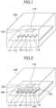
- FIG. 1 and FIG. 2 illustrate an outline of the information processing apparatus that includes a printed wiring board of this example.
- An information processing apparatus 100 illustrated in FIG. 1 includes a printed wiring board 101. To the printed wiring board 101, one memory controller 110 and a plurality of memory devices 111 to 119 are directly mounted. The plurality of memory devices 111 to 119 are mounted on both surfaces of the printed wiring board 101. That is, FIG. 1 illustrates only the memory devices 111, 113, 115, 117, and 119 mounted on the front surface of the printed wiring board 101 and does not illustrate the memory devices 112, 114, 116, and 118 mounted on the back surface of the printed wiring board 101. The same applies to FIG. 2 described later.
- a multi-point wiring 102 couples between the memory controller 110 and the respective memory devices 111 to 119.
- the respective memory devices 111 to 119 are DDR SDRAMs, and the memory controller 110 controls writing and reading of data in the respective memory devices 111 to 119. To perform this control, the memory controller 110 transmits address, command, and control signals to the respective memory devices 111 to 119 via the multi-point wiring 102.
- FIG. 2 illustrates a configuration of an information processing apparatus 100' having another configuration.
- a connector 103 is mounted to the printed wiring board 101.
- the plurality of memory devices 111 to 119 mounted on a sub-substrate 106 are coupled.
- the sub-substrate 106 on which the plurality of memory devices 111 to 119 are thus mounted is referred to as a Dual Inline Memory Module (DIMM) card or the like.
- DIMM Dual Inline Memory Module
- the memory controller 110 is directly mounted to the printed wiring board 101.
- the plurality of memory devices 111 to 119 are mounted on both surfaces of the printed wiring board 101, but FIG. 2 illustrates only the memory devices 111, 113, 115, 117, and 119 mounted on the front surface.
- the memory controller 110 transmits the address, command, and control signals to the respective memory devices 111 to 119 via the multi-point wiring 102.
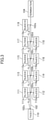
- FIG. 3 illustrates an exemplary configuration of the multi-point wiring 102 formed on the printed wiring board 101.
- the multi-point wiring 102 of this example may be applied in both cases where the memory devices 111 to 119 are directly mounted to the printed wiring board 101 as illustrated in FIG. 1 and where the memory devices 111 to 119 are mounted to the printed wiring board 101 via the connector 103 as illustrated in FIG. 2 .
- a starting end (one end) 102x of the multi-point wiring 102 is coupled to the memory controller 110, which is a transmitting circuit of the address, command, and control signals.
- Branch points 102a, 102b, 102c, 102d, and 102e are provided at a plurality of positions in the multi-point wiring 102, and a termination resistor 104 is coupled at a termination (the other end) .
- Wirings branched at the respective branch points 102a to 102e are coupled to coupling portions 111a to 119a of the respective memory devices 111 to 119.
- the respective memory devices 111 to 119 are dividedly disposed on the front surface and the back surface of the printed wiring board 101. Accordingly, at the respective branch points 102a, 102b, 102c, and 102d, branches to the memory devices 111, 113, 115, and 117, which are disposed on the front surface side, and branches to the memory devices 112, 114, 116, and 118, which are disposed on the back surface side, are formed. At the branch point 102e, only a branch to the memory device 119 on the front surface side is formed.
- a distance from the starting end 102x of the multi-point wiring 102 to the first branch point 102a is defined as a distance TL0.
- a distance from the branch point 102a of the multi-point wiring 102 to the adjacent branch point 102b is defined as a distance TL1
- distances between the branch points 102b and 102c, the branch points 102c and 102d, and the branch points 102d and 102e are defined as distances TL2, TL3, and TL4, respectively.
- FIG. 3 illustrates the multi-point wiring 102 in a linear shape, but is actually disposed so as to appropriately have bent portions according to the shape of the printed wiring board 101 and the arranged positions of the respective memory devices 111 to 119. While FIG. 3 illustrates the respective distances TL0 to TL4 having approximately equal distances, but the distances are actually not the same as described below.
- the following values are set to the respective distances TL0 to TL4 of the multi-point wiring 102.
- the distance TL0 from the starting end 102x of the multi-point wiring 102 as the coupling point with the memory controller 110 to the first branch point 102a is set to a value longer than the distance TL1 from the first branch point 102a to the next branch point 102b.
- the distance TL1 from the first branch point 102a to the next branch point 102b is set to a value longer than the distances TL2, TL3, and TL4 between the subsequent adjacent branch points 102b, 102c, 102d, and 102e.
- the distances TL1 to TL4 between the respective adjacent branch points 102a to 102e are set to gradually decreasing values as away from the starting end 102x, and thus the respective distances TL0 to TL4 are set at non-equal spacing pitches.
- lengths of branch wirings from the respective branch points 102a to 102e of the multi-point wiring 102 to the coupling portions 111a to 119a of the respective memory devices 111 to 119 are preferably set to be an approximately same length.
- a distance from the starting end 102x of the multi-point wiring 102 to the coupling portion 119a of the memory device 119 at the position farthest from the starting end 102x is set to have a length equal to or less than a length regulated by a vendor of the memory device as a wiring length connectable to the memory devices 111 to 119.
- the connector 103 when the connector 103 is mounted to the printed wiring board 101, the connector 103 is preferably present at the branch wirings between the respective branch points 102a to 102e and the coupling portions 111a to 119a of the respective memory devices 111 to 119.
- FIG. 4 illustrates the examples of the received waveforms at the coupling portions 111a to 119a of the respective memory devices 111 to 119 in the case where the respective distances TL0 to TL4 of the multi-point wiring 102 are set as described above.
- FIG. 5 illustrates examples of received waveforms at the coupling portions 111a to 119a of the respective memory devices 111 to 119 in the case where the respective distances TL0 to TL4 of the multi-point wiring 102 are set to be different lengths for reference.
- the respective distances TL0 to TL4 of the multi-point wiring 102 are set to the following values.
- IC2, IC3, IC4, IC5, IC6, IC7, IC8, IC9, and IC10 denote the received waveforms at the coupling portions 111a to 119a of the nine memory devices 111 to 119.
- FIG. 4 and FIG. 5 illustrate the waveforms appearing at the coupling portions 111a to 119a of the respective memory devices 111 to 119 (IC2 to IC10) as eye patterns.
- the eye pattern is generated by overlapping a large number of sampled transitions of signal waveforms for display.
- the waveform When a width of a line in the eye pattern is narrow (in the case of what is called a pattern of an open eye mask), the waveform has a good quality, and when the width of the line is wide (in the case of what is called a pattern of a closed eye mask), the waveform is distorted and has a poor quality. From the eye patterns of FIG. 4 and FIG. 5 , it is seen that the eye pattern of FIG. 4 forms the waveform having the better quality than that of the eye pattern of FIG. 5 .
- FIG. 6A and FIG. 6B illustrate examples of the eye masks in the eye patterns.
- FIG. 6A and FIG. 6B illustrate a relationship between a threshold and a waveform in DDR memory interfaces applied to the DDR SDRAMs as the memory devices 111 to 119 of this example.
- FIG. 6A illustrates the equal spacing pitch, that is, the eye pattern of the memory device 113 (IC4) in the example of FIG. 5 .
- FIG. 6B illustrates the non-equal spacing pitch, that is, the eye pattern of the memory device 113 (IC4) in this example illustrated in FIG. 4 .
- Vih(ac) and Vil(ac) denote threshold voltages used in a setup time
- Vih(dc) and Vil(dc) denote threshold voltages used in a hold time.
- the eye masks are regulated by these threshold voltages Vih(ac), Vil(ac), Vih(dc), and Vil(dc).
- the eye mask has a trapezoidal shape.
- Distances M1 and M2 between the trapezoidal eye masks and the waveforms illustrated in FIG. 6A and FIG. 6B are margins.
- the larger the margin for the eye mask is the more it is preferred.
- the smaller the margin for the eye mask is the higher a possibility of failing to correctly receive data is.
- the margin M2 to the eye mask in this example is larger than the margin M1 to the eye mask at the equal spacing pitch.
- FIG. 6A and FIG. 6B compare the eye patterns of the memory device 113 (IC4) coupled to the approximately middle of the multi-point wiring 102.
- the margins to the eye masks are considerably small in the memory devices except for the memory devices 111 and 112 (IC2 and IC3), which are coupled to the first branch point 102a.
- the respective memory devices 111 to 119 coupled with the multi-point wiring 102 of this example can excellently receive the data from the memory controller 110 free from an error, and this contributes to a stable operation and improvement in reliability as the information processing apparatus.
- the enlargement of the margin for the eye mask is achieved by reducing simultaneous superimposition of a ring-back component and a capacity reflection component appearing in the eye pattern.
- the ring-back component and the capacity reflection component from the influence of the received signal in other memory devices are superimposed on the received signals in the respective memory devices approximately at the same time.
- the margin for the eye mask narrows.
- the multi-point wiring 102 is at the non-equal spacing pitch, the ring-back component and the capacity reflection component are not simultaneously superimposed, and as illustrated in FIG. 6B , the margin for the eye mask widens.
- the memory controller 110 can stably transmit the address, command, control signals to the respective memory devices 111 to 119 free from error. Accordingly, the information processing apparatus 100 (100') including the memory controller 110 and the memory devices 111 to 119 improve reliability.
- the present invention is not limited to the above-described exemplary embodiments but includes various modifications.
- the relationship between the distances TL0 to TL4 meet the distances TL0 > TL 1 > TL2 > TL3 > TL4.
- the distance TL1 is configured to have a value longer than the distances TL2, TL3, and TL4 between the subsequent branch points 102b and 102c, the branch points 102c and 102d, and the branch points 102d and 102e, an effect of the wide margin for the eye mask is provided.
- the distances TL2, TL3, and TL4 may be the same value.
- the distances are preferably set so as to meet TL0 > TL1 > TL2 > TL3 > TL4 as described in the above-described exemplary embodiment.
- the nine memory devices 111 to 119 are disposed, this is merely an example, and any number of the memory devices may be used.
- the three memory devices 111, 113, and 115 may be prepared, and the three memory devices 111, 113, and 115 may be coupled to the multi-point wiring 102. In this case, it is only necessary to set the distances TL0, TL1, and TL2 to meet the relationship TL0 > TL1 > TL2.
- the memory devices 111 to 119 are disposed on both surfaces of the printed circuit board, this is merely an example, and the memory devices may be disposed on one surface.
- the multi-point wiring 102 of this example is applicable to both of the case where the memory devices 111 to 119 are directly coupled without via the connector as illustrated in FIG. 1 and the case where the memory devices 111 to 119 are coupled using the connector 103 as illustrated in FIG. 2 .
- the printed wiring board 101 that includes the multi-point wiring 102 of this example may be coated with varnish to reduce corrosion or the like together with the memory controller 110 and the respective memory devices 111 to 119 mounted to the printed wiring board 101. This allows excellently using the printed wiring board 101 under corrosive gas environment.
- the connector is preferably not disposed as the configuration where the memory devices 111 to 119 are directly mounted to the printed wiring board 101.
- the multi-point wiring 102 of this example is used for coupling between the memory controller and the plurality of memory devices (DDR SDRAMs).
- DDR SDRAMs memory devices
- the similar effects can be obtained also in a case where the present invention is applied to a multi-point wiring that couples another one transmitting circuit component and a plurality of receiving circuit components.
Landscapes
- Engineering & Computer Science (AREA)
- Theoretical Computer Science (AREA)
- Microelectronics & Electronic Packaging (AREA)
- General Engineering & Computer Science (AREA)
- Physics & Mathematics (AREA)
- General Physics & Mathematics (AREA)
- Manufacturing & Machinery (AREA)
- Computer Hardware Design (AREA)
- Structure Of Printed Boards (AREA)
- Memory System (AREA)
Abstract
Description
- The present invention contains subject matter related to
Japanese Patent Application JP2020-125150 - The present invention relates to a printed wiring board and an information processing apparatus.
- A memory device mounted to an information processing apparatus includes, for example, a plurality of Synchronous Dynamic Random Access Memories (SDRAMs) and a memory controller (controller Large Scale Integration: LSI) that controls writing and reading of the SDRAMs . As the SDRAM, a Double-Data-Rate SDRAM (DDR SDRAM) is generally used.
- The plurality of SDRAMs and the memory controller are mounted to a printed wiring board.
- The memory controller transmits address (Add), command (Cmd), and control (Ctrl) signals to each SDRAM in a wiring pattern formed on the printed wiring board referred to as a multi-point wiring. In the multi-point wiring in this case, the memory controller is a transmission end and the plurality of SDRAMs are reception ends.
- To couple the memory controller and the plurality of SDRAMs by the multi-point wiring, a wiring pitch and a wiring length need to be appropriately selected. An inappropriate wiring length generates reflection in a negative direction in the transmission signal due to a capacitive component (capacitance) that the SDRAM has. Therefore, the reflection component is superimposed on the received waveform of the SDRAM and causes a ring-back, and this makes it difficult to appropriately maintain a digital threshold. This results in decrease in voltage margin, failing to correctly transmit the signal.
Japanese Unexamined Patent Application Publication No. 2009-86841 - To improve performance of the information processing apparatus, a high speed and a large capacity are indispensable for the printed circuit board that includes the memories, such as the SDRAMs. Here, the above-described multi-point wiring has a plurality of branches and the plurality of memories are coupled to the multi-point wiring. Therefore, the multi-point wiring is likely to be accompanied by a waveform distortion due to undesired reflection, and improvement in waveform quality and improvement in reliability are objects.
- For the objects, the technique described in
Japanese Unexamined Patent Application Publication No. 2009-86841 - However, as described above, the technique described in
Japanese Unexamined Patent Application Publication No. 2009-86841 - Meanwhile, the maximum wiring length or the like of the component, such as the memory controller, is determined as a specification designated by a vendor, and the above-described multi-point wiring also needs to be designed to have the wiring length meeting the specification.
- As a specific example, there is a memory controller (LSI) whose difference in wiring length between clock, address, command, and control signals; and a data strobe signal is regulated to be within 50.8 mm and the wiring length of the data strobe signal is restricted to be within 100 mm. In the case, even when it is attempted to decrease a linear distance to the SDRAM at the farthest end from the memory controller, it is difficult because of the following reasons.
- That is, when the total length of the address, command, and control signals lengthens, after the arrangement pitches of the SDRAMs are decreased, a large number of bent portions referred to as a meander wiring need to be provided in the wiring that connect between the respective SDRAMs to lengthen the distance. Furthermore, to reduce a crosstalk, it is necessary to provide large spaces between the respective wirings, and as a result, configuring the regulated wiring length is difficult.
- An object of the present invention is to provide a printed wiring board that allows transmitting excellent signals without lengthening a total wiring length of a multi-point wiring and an information processing apparatus that includes the printed wiring board.
- To solve the above-described problems, for example, the configurations described in the claims are employed.
- While this application includes a plurality of means to solve the problems, one example is a printed wiring board in which one transmitting circuit and N (N is an integer of 3 or more) receiving circuits are coupled by a multi-point wiring. First to N-th branch points are provided in sequence in the multi-point wiring having one end coupled to the transmitting circuit. Wirings branched at the respective branch points is coupled to the respective receiving circuits.
- A wiring length from a coupling point of the transmitting circuit in the multi-point wiring to a first branch point is configured to be longer than a wiring length from the first branch point to a second branch point. Wiring lengths between the adjacent branch points at and after the second branch point are configured to be shorter than the wiring length from the first branch point to the second branch point.
- With the present invention, in the multi-point wiring applied to a wiring of memory devices or the like, a voltage margin for an external noise, such as a crosstalk, can be ensured, and therefore high waveform quality can be obtained and a signal can be excellently transmitted to a plurality of receiving circuits.
- Problems, configurations, and effects other than ones described above will be clarified in the following explanation of embodiments.
-
-
FIG. 1 is a block diagram illustrating an outline of an information processing apparatus (example 1) that applies a printed wiring board according to one exemplary embodiment of the present invention; -
FIG. 2 is a block diagram illustrating an outline of an information processing apparatus (example 2) that applies the printed wiring board according to one exemplary embodiment of the present invention; -
FIG. 3 is a drawing illustrating an example of a wiring structure of the printed wiring board according to one exemplary embodiment of the present invention; -
FIG. 4 is a drawing illustrating an example of a received waveform in each memory device when transmission is performed in the printed wiring board according to one exemplary embodiment of the present invention; -
FIG. 5 is a drawing illustrating an example of a received waveform in each memory device at an equal spacing pitch where the present invention is not applied; and -
FIG. 6A and FIG. 6B are drawings for a comparison between a waveform at the equal spacing pitch (FIG. 6A ) and a waveform at a non-equal spacing pitch (FIG. 6B ). - Hereinafter, one exemplary embodiment of the present invention (hereinafter referred to as "this example" will be described with reference to the attached drawings. Configuration of Information Processing Apparatus
-
FIG. 1 and FIG. 2 illustrate an outline of the information processing apparatus that includes a printed wiring board of this example. - An
information processing apparatus 100 illustrated inFIG. 1 includes a printedwiring board 101. To the printedwiring board 101, onememory controller 110 and a plurality ofmemory devices 111 to 119 are directly mounted. The plurality ofmemory devices 111 to 119 are mounted on both surfaces of the printedwiring board 101. That is,FIG. 1 illustrates only thememory devices wiring board 101 and does not illustrate thememory devices wiring board 101. The same applies toFIG. 2 described later. - A
multi-point wiring 102 couples between thememory controller 110 and therespective memory devices 111 to 119. - The
respective memory devices 111 to 119 are DDR SDRAMs, and thememory controller 110 controls writing and reading of data in therespective memory devices 111 to 119. To perform this control, thememory controller 110 transmits address, command, and control signals to therespective memory devices 111 to 119 via themulti-point wiring 102. -
FIG. 2 illustrates a configuration of an information processing apparatus 100' having another configuration. - In the information processing apparatus 100' illustrated in
FIG. 2 , aconnector 103 is mounted to the printedwiring board 101. To theconnector 103, the plurality ofmemory devices 111 to 119 mounted on asub-substrate 106 are coupled. Thesub-substrate 106 on which the plurality ofmemory devices 111 to 119 are thus mounted is referred to as a Dual Inline Memory Module (DIMM) card or the like. - The
memory controller 110 is directly mounted to the printedwiring board 101. - Similarly to the
information processing apparatus 100 illustrated inFIG. 1 , in the information processing apparatus 100' illustrated inFIG. 2 , the plurality ofmemory devices 111 to 119 are mounted on both surfaces of the printedwiring board 101, butFIG. 2 illustrates only thememory devices - In the printed
wiring board 101 illustrated inFIG. 2 as well, thememory controller 110 transmits the address, command, and control signals to therespective memory devices 111 to 119 via themulti-point wiring 102. -
FIG. 3 illustrates an exemplary configuration of themulti-point wiring 102 formed on the printedwiring board 101. Themulti-point wiring 102 of this example may be applied in both cases where thememory devices 111 to 119 are directly mounted to the printedwiring board 101 as illustrated inFIG. 1 and where thememory devices 111 to 119 are mounted to the printedwiring board 101 via theconnector 103 as illustrated inFIG. 2 . - To the
memory controller 110, which is a transmitting circuit of the address, command, and control signals, a starting end (one end) 102x of themulti-point wiring 102 is coupled.Branch points multi-point wiring 102, and atermination resistor 104 is coupled at a termination (the other end) . - Wirings branched at the
respective branch points 102a to 102e are coupled tocoupling portions 111a to 119a of therespective memory devices 111 to 119. As already described, therespective memory devices 111 to 119 are dividedly disposed on the front surface and the back surface of the printedwiring board 101. Accordingly, at therespective branch points memory devices memory devices branch point 102e, only a branch to thememory device 119 on the front surface side is formed. - Here, in this example, as illustrated in
FIG. 3 , a distance from the startingend 102x of themulti-point wiring 102 to thefirst branch point 102a is defined as a distance TL0. A distance from thebranch point 102a of themulti-point wiring 102 to theadjacent branch point 102b is defined as a distance TL1, and hereinafter, distances between the branch points 102b and 102c, the branch points 102c and 102d, and the branch points 102d and 102e are defined as distances TL2, TL3, and TL4, respectively. -
FIG. 3 illustrates themulti-point wiring 102 in a linear shape, but is actually disposed so as to appropriately have bent portions according to the shape of the printedwiring board 101 and the arranged positions of therespective memory devices 111 to 119. WhileFIG. 3 illustrates the respective distances TL0 to TL4 having approximately equal distances, but the distances are actually not the same as described below. - In this example, the following values are set to the respective distances TL0 to TL4 of the
multi-point wiring 102. - TL0: 90.2 mm
- TL1: 24.1 mm
- TL2: 22.3 mm
- TL3: 20.6 mm
- TL4: 17.2 mm
- Thus, the distance TL0 from the starting
end 102x of themulti-point wiring 102 as the coupling point with thememory controller 110 to thefirst branch point 102a is set to a value longer than the distance TL1 from thefirst branch point 102a to thenext branch point 102b. - Additionally, the distance TL1 from the
first branch point 102a to thenext branch point 102b is set to a value longer than the distances TL2, TL3, and TL4 between the subsequentadjacent branch points - Furthermore, in this example, the distances TL1 to TL4 between the respective
adjacent branch points 102a to 102e are set to gradually decreasing values as away from the startingend 102x, and thus the respective distances TL0 to TL4 are set at non-equal spacing pitches. Note that lengths of branch wirings from therespective branch points 102a to 102e of themulti-point wiring 102 to thecoupling portions 111a to 119a of therespective memory devices 111 to 119 are preferably set to be an approximately same length. - Note that a distance from the starting
end 102x of themulti-point wiring 102 to thecoupling portion 119a of thememory device 119 at the position farthest from the startingend 102x is set to have a length equal to or less than a length regulated by a vendor of the memory device as a wiring length connectable to thememory devices 111 to 119. - As illustrated in
FIG. 2 , when theconnector 103 is mounted to the printedwiring board 101, theconnector 103 is preferably present at the branch wirings between therespective branch points 102a to 102e and thecoupling portions 111a to 119a of therespective memory devices 111 to 119. -
FIG. 4 illustrates the examples of the received waveforms at thecoupling portions 111a to 119a of therespective memory devices 111 to 119 in the case where the respective distances TL0 to TL4 of themulti-point wiring 102 are set as described above. - For comparison,
FIG. 5 illustrates examples of received waveforms at thecoupling portions 111a to 119a of therespective memory devices 111 to 119 in the case where the respective distances TL0 to TL4 of themulti-point wiring 102 are set to be different lengths for reference. In the examples ofFIG. 5 , the respective distances TL0 to TL4 of themulti-point wiring 102 are set to the following values. - TL0: 90.2 mm
- TL1: 17.25 mm
- TL2: 17.25 mm
- TL3: 17.25 mm
- TL4: 17.25 mm
- That is, in the examples of
FIG. 5 , although the point that the distance TL0 is the longest is same as this example illustrated inFIG. 4 , the other distances TL1 to TL4 are all set to be an equal interval with the same length. - In
FIG. 4 andFIG. 5 , IC2, IC3, IC4, IC5, IC6, IC7, IC8, IC9, and IC10 denote the received waveforms at thecoupling portions 111a to 119a of the ninememory devices 111 to 119. -
FIG. 4 andFIG. 5 illustrate the waveforms appearing at thecoupling portions 111a to 119a of therespective memory devices 111 to 119 (IC2 to IC10) as eye patterns. The eye pattern is generated by overlapping a large number of sampled transitions of signal waveforms for display. - When a width of a line in the eye pattern is narrow (in the case of what is called a pattern of an open eye mask), the waveform has a good quality, and when the width of the line is wide (in the case of what is called a pattern of a closed eye mask), the waveform is distorted and has a poor quality. From the eye patterns of
FIG. 4 andFIG. 5 , it is seen that the eye pattern ofFIG. 4 forms the waveform having the better quality than that of the eye pattern ofFIG. 5 . -
FIG. 6A and FIG. 6B illustrate examples of the eye masks in the eye patterns. - That is,
FIG. 6A and FIG. 6B illustrate a relationship between a threshold and a waveform in DDR memory interfaces applied to the DDR SDRAMs as thememory devices 111 to 119 of this example. -
FIG. 6A illustrates the equal spacing pitch, that is, the eye pattern of the memory device 113 (IC4) in the example ofFIG. 5 .FIG. 6B illustrates the non-equal spacing pitch, that is, the eye pattern of the memory device 113 (IC4) in this example illustrated inFIG. 4 . - In
FIG. 6A , Vih(ac) and Vil(ac) denote threshold voltages used in a setup time, and Vih(dc) and Vil(dc) denote threshold voltages used in a hold time. - The eye masks are regulated by these threshold voltages Vih(ac), Vil(ac), Vih(dc), and Vil(dc). In the DDR memory interface, since the threshold voltages Vih(dc) and Vil(dc) used in the hold time are lower than the threshold voltages Vih(ac) and Vil (ac) used in the setup time, the eye mask has a trapezoidal shape.
- Distances M1 and M2 between the trapezoidal eye masks and the waveforms illustrated in
FIG. 6A and FIG. 6B are margins. To properly receive data, the larger the margin for the eye mask is, the more it is preferred. Conversely, the smaller the margin for the eye mask is, the higher a possibility of failing to correctly receive data is. - Here, as seen from the comparison between
FIG. 6B as the eye pattern of this example (non-equal spacing pitch) andFIG. 6A as the eye pattern at the equal spacing pitch as a comparative example, the margin M2 to the eye mask in this example is larger than the margin M1 to the eye mask at the equal spacing pitch. -
FIG. 6A and FIG. 6B compare the eye patterns of the memory device 113 (IC4) coupled to the approximately middle of themulti-point wiring 102. In the case of the equal spacing pitch illustrated inFIG. 5 , the margins to the eye masks are considerably small in the memory devices except for thememory devices 111 and 112 (IC2 and IC3), which are coupled to thefirst branch point 102a. - Meanwhile, in the case of the non-equal spacing pitch of this example illustrated in
FIG. 4 , although the slight decrease in margin is observed in thememory devices - Accordingly, the
respective memory devices 111 to 119 coupled with themulti-point wiring 102 of this example can excellently receive the data from thememory controller 110 free from an error, and this contributes to a stable operation and improvement in reliability as the information processing apparatus. - The enlargement of the margin for the eye mask is achieved by reducing simultaneous superimposition of a ring-back component and a capacity reflection component appearing in the eye pattern.
- That is, when the distances TL1 to TL4 between the respective branch points in the
multi-point wiring 102 are at the equal spacing pitch, the ring-back component and the capacity reflection component from the influence of the received signal in other memory devices are superimposed on the received signals in the respective memory devices approximately at the same time. Thus, at the equal spacing pitch illustrated inFIG. 6A , the margin for the eye mask narrows. - On the other hand, in this example, since the
multi-point wiring 102 is at the non-equal spacing pitch, the ring-back component and the capacity reflection component are not simultaneously superimposed, and as illustrated inFIG. 6B , the margin for the eye mask widens. - As described above, with the printed
wiring board 101 including themulti-point wiring 102 of this example, thememory controller 110 can stably transmit the address, command, control signals to therespective memory devices 111 to 119 free from error. Accordingly, the information processing apparatus 100 (100') including thememory controller 110 and thememory devices 111 to 119 improve reliability. - The present invention is not limited to the above-described exemplary embodiments but includes various modifications.
- For example, in the above-described exemplary embodiment, the relationship between the distances TL0 to TL4 meet the distances TL0 > TL 1 > TL2 > TL3 > TL4. In contrast to this, when at least the distance TL0 from the starting
end 102x to thefirst branch point 102a is configured to be longer than the distance TL1 from thefirst branch point 102a to thenext branch point 102b, and the distance TL1 is configured to have a value longer than the distances TL2, TL3, and TL4 between the subsequent branch points 102b and 102c, the branch points 102c and 102d, and the branch points 102d and 102e, an effect of the wide margin for the eye mask is provided. - That is, as long as at least the distance TL0 from the starting
end 102x to thefirst branch point 102a is longer than the distance TL1 from thefirst branch point 102a to thenext branch point 102b, and the distance TL1 is longer than the distances TL2, TL3, and TL4, the distances TL2, TL3, and TL4 may be the same value. However, the distances are preferably set so as to meet TL0 > TL1 > TL2 > TL3 > TL4 as described in the above-described exemplary embodiment. - While the nine
memory devices 111 to 119 are disposed, this is merely an example, and any number of the memory devices may be used. For example, the threememory devices memory devices multi-point wiring 102. In this case, it is only necessary to set the distances TL0, TL1, and TL2 to meet the relationship TL0 > TL1 > TL2. - While the
memory devices 111 to 119 are disposed on both surfaces of the printed circuit board, this is merely an example, and the memory devices may be disposed on one surface. - The
multi-point wiring 102 of this example is applicable to both of the case where thememory devices 111 to 119 are directly coupled without via the connector as illustrated inFIG. 1 and the case where thememory devices 111 to 119 are coupled using theconnector 103 as illustrated inFIG. 2 . - The printed
wiring board 101 that includes themulti-point wiring 102 of this example may be coated with varnish to reduce corrosion or the like together with thememory controller 110 and therespective memory devices 111 to 119 mounted to the printedwiring board 101. This allows excellently using the printedwiring board 101 under corrosive gas environment. When applying the corrosion-resistant coating, when possible, as illustrated inFIG. 1 , the connector is preferably not disposed as the configuration where thememory devices 111 to 119 are directly mounted to the printedwiring board 101. - Furthermore, the
multi-point wiring 102 of this example is used for coupling between the memory controller and the plurality of memory devices (DDR SDRAMs). However, the similar effects can be obtained also in a case where the present invention is applied to a multi-point wiring that couples another one transmitting circuit component and a plurality of receiving circuit components.
Claims (6)
- A printed wiring board in which a transmitting circuit and N (N is an integer of 3 or more) receiving circuits are coupled by a multi-point wiring (102), wherein
first to N-th branch points are provided in sequence in the multi-point wiring (102) having one end coupled to the transmitting circuit, wirings branched at the respective branch points are coupled to the respective receiving circuits,
a wiring length from a coupling point of the transmitting circuit in the multi-point wiring (102) to a first branch point (102a) is configured to be longer than a wiring length from the first branch point (102a) to a second branch point, and
wiring lengths between the adjacent branch points at and after the second branch point are configured to be shorter than the wiring length from the first branch point (102a) to the second branch point. - The printed wiring board according to claim 1, wherein
the wiring lengths between the adjacent branch points at and after the second branch point are further configured to be the wiring lengths that decrease in sequence as away from the coupling point of the transmitting circuit. - The printed wiring board according to claim 1, wherein
the transmitting circuit is a memory controller (110), and the receiving circuits are memory devices (111, 112, 113, 114, 115, 116, 117, 118, 119), and
the multi-point wiring (102) is a wiring that transmits address, command, and control signals from the memory controller (110) to the memory devices (111, 112, 113, 114, 115, 116, 117, 118, 119). - The printed wiring board according to claim 1, wherein
the multi-point wiring (102) is directly coupled to the memory devices (111, 112, 113, 114, 115, 116, 117, 118, 119) without via any connector (103). - The printed wiring board according to claim 4, wherein
a corrosion-resistant coating is applied on the printed wiring board to which the memory controller (110) and the memory devices (111, 112, 113, 114, 115, 116, 117, 118, 119) are mounted. - An information processing apparatus (100, 100') that includes a printed wiring board (101) in which a transmitting circuit and N (N is an integer of 3 or more) receiving circuits are coupled by a multi-point wiring (102), wherein
in the printed wiring board (101), first to N-th branch points are provided in sequence in the multi-point wiring (102) having one end coupled to the transmitting circuit, wirings branched at the respective branch points are coupled to the respective receiving circuits,
a wiring length from a coupling point of the transmitting circuit in the multi-point wiring (102) to a first branch point (102a) is configured to be longer than a wiring length from the first branch point (102a) to a second branch point, and
wiring lengths between the adjacent branch points at and after the second branch point are configured to be shorter than the wiring length from the first branch point (102a) to the second branch point.
Applications Claiming Priority (1)
| Application Number | Priority Date | Filing Date | Title |
|---|---|---|---|
| JP2020125150A JP7469978B2 (en) | 2020-07-22 | 2020-07-22 | Printed wiring board and information processing device |
Publications (2)
| Publication Number | Publication Date |
|---|---|
| EP3944244A1 true EP3944244A1 (en) | 2022-01-26 |
| EP3944244B1 EP3944244B1 (en) | 2023-08-30 |
Family
ID=76744610
Family Applications (1)
| Application Number | Title | Priority Date | Filing Date |
|---|---|---|---|
| EP21182731.6A Active EP3944244B1 (en) | 2020-07-22 | 2021-06-30 | Printed wiring board and information processing apparatus |
Country Status (4)
| Country | Link |
|---|---|
| US (1) | US11612055B2 (en) |
| EP (1) | EP3944244B1 (en) |
| JP (1) | JP7469978B2 (en) |
| CN (1) | CN113971141B (en) |
Citations (2)
| Publication number | Priority date | Publication date | Assignee | Title |
|---|---|---|---|---|
| JP2009086841A (en) | 2007-09-28 | 2009-04-23 | Elpida Memory Inc | Address line wiring structure and printed wiring board having the same |
| US20120250264A1 (en) * | 2011-03-28 | 2012-10-04 | Elpida Memory, Inc. | Memory module having memory chip and register buffer |
Family Cites Families (8)
| Publication number | Priority date | Publication date | Assignee | Title |
|---|---|---|---|---|
| KR100399594B1 (en) * | 2000-05-04 | 2003-09-26 | 삼성전자주식회사 | system board and impedance control method thereof |
| JP2003044189A (en) * | 2001-07-30 | 2003-02-14 | Fujitsu Ltd | Information processing apparatus, circuit board, and module connection method |
| JP3742051B2 (en) * | 2002-10-31 | 2006-02-01 | エルピーダメモリ株式会社 | Memory module, memory chip, and memory system |
| WO2009019746A1 (en) * | 2007-08-03 | 2009-02-12 | Fujitsu Limited | Communication device, communication system, and communication method |
| CN102177550B (en) * | 2008-08-08 | 2014-03-12 | 惠普开发有限公司 | Independently controlled virtual memory devices in memory modules |
| JP2011205366A (en) * | 2010-03-25 | 2011-10-13 | Yokogawa Electric Corp | Reception circuit |
| JP5925352B2 (en) * | 2014-04-14 | 2016-05-25 | キヤノン株式会社 | Printed circuit board and printed wiring board |
| CN110931974A (en) * | 2019-12-03 | 2020-03-27 | 惠州Tcl移动通信有限公司 | Antenna impedance matching circuit, antenna system, printed circuit board and mobile terminal |
-
2020
- 2020-07-22 JP JP2020125150A patent/JP7469978B2/en active Active
-
2021
- 2021-06-01 CN CN202110610116.7A patent/CN113971141B/en active Active
- 2021-06-30 EP EP21182731.6A patent/EP3944244B1/en active Active
- 2021-07-20 US US17/380,079 patent/US11612055B2/en active Active
Patent Citations (2)
| Publication number | Priority date | Publication date | Assignee | Title |
|---|---|---|---|---|
| JP2009086841A (en) | 2007-09-28 | 2009-04-23 | Elpida Memory Inc | Address line wiring structure and printed wiring board having the same |
| US20120250264A1 (en) * | 2011-03-28 | 2012-10-04 | Elpida Memory, Inc. | Memory module having memory chip and register buffer |
Also Published As
| Publication number | Publication date |
|---|---|
| US11612055B2 (en) | 2023-03-21 |
| CN113971141B (en) | 2024-11-22 |
| EP3944244B1 (en) | 2023-08-30 |
| CN113971141A (en) | 2022-01-25 |
| JP2022021534A (en) | 2022-02-03 |
| JP7469978B2 (en) | 2024-04-17 |
| US20220030706A1 (en) | 2022-01-27 |
Similar Documents
| Publication | Publication Date | Title |
|---|---|---|
| US6125419A (en) | Bus system, printed circuit board, signal transmission line, series circuit and memory module | |
| US7274583B2 (en) | Memory system having multi-terminated multi-drop bus | |
| US6580295B2 (en) | Signal transmission system | |
| US7035116B2 (en) | Memory system and memory subsystem | |
| US7095661B2 (en) | Semiconductor memory module, memory system, circuit, semiconductor device, and DIMM | |
| US7047384B2 (en) | Method and apparatus for dynamic timing of memory interface signals | |
| US20050105318A1 (en) | Memory module, memory chip, and memory system | |
| CN102473148A (en) | Method and system for synchronizing address and control signals in threaded memory modules | |
| US6487086B2 (en) | Circuit module | |
| US8036011B2 (en) | Memory module for improving signal integrity and computer system having the same | |
| KR100941024B1 (en) | Memory operating devices, systems and methods | |
| US8332680B2 (en) | Methods and systems for operating memory in two modes | |
| EP3944244B1 (en) | Printed wiring board and information processing apparatus | |
| US6839786B2 (en) | Information processing system with memory modules of a serial bus architecture | |
| US8031504B2 (en) | Motherboard and memory device thereof | |
| JP2007164599A (en) | Memory module | |
| JP2005085267A (en) | Circuit for memory module address bus and system for addressing memory module | |
| KR100355714B1 (en) | Digital Information Processing System With A Modular Bus Architecture | |
| JP3546613B2 (en) | Circuit board | |
| KR101526318B1 (en) | A memory system comprising a memory board on which a stub resistor is formed on a main board | |
| JP3543541B2 (en) | Signal transmission equipment | |
| JP2004187312A (en) | Signal transmission equipment | |
| US20060056214A1 (en) | Memory module with reduced input clock skew | |
| US8161219B2 (en) | Distributed command and address bus architecture for a memory module having portions of bus lines separately disposed | |
| CN109154923A (en) | Circuit board based on memory |
Legal Events
| Date | Code | Title | Description |
|---|---|---|---|
| PUAI | Public reference made under article 153(3) epc to a published international application that has entered the european phase |
Free format text: ORIGINAL CODE: 0009012 |
|
| STAA | Information on the status of an ep patent application or granted ep patent |
Free format text: STATUS: REQUEST FOR EXAMINATION WAS MADE |
|
| 17P | Request for examination filed |
Effective date: 20211001 |
|
| AK | Designated contracting states |
Kind code of ref document: A1 Designated state(s): AL AT BE BG CH CY CZ DE DK EE ES FI FR GB GR HR HU IE IS IT LI LT LU LV MC MK MT NL NO PL PT RO RS SE SI SK SM TR |
|
| GRAP | Despatch of communication of intention to grant a patent |
Free format text: ORIGINAL CODE: EPIDOSNIGR1 |
|
| STAA | Information on the status of an ep patent application or granted ep patent |
Free format text: STATUS: GRANT OF PATENT IS INTENDED |
|
| INTG | Intention to grant announced |
Effective date: 20230331 |
|
| GRAS | Grant fee paid |
Free format text: ORIGINAL CODE: EPIDOSNIGR3 |
|
| GRAA | (expected) grant |
Free format text: ORIGINAL CODE: 0009210 |
|
| STAA | Information on the status of an ep patent application or granted ep patent |
Free format text: STATUS: THE PATENT HAS BEEN GRANTED |
|
| AK | Designated contracting states |
Kind code of ref document: B1 Designated state(s): AL AT BE BG CH CY CZ DE DK EE ES FI FR GB GR HR HU IE IS IT LI LT LU LV MC MK MT NL NO PL PT RO RS SE SI SK SM TR |
|
| REG | Reference to a national code |
Ref country code: GB Ref legal event code: FG4D |
|
| REG | Reference to a national code |
Ref country code: CH Ref legal event code: EP |
|
| REG | Reference to a national code |
Ref country code: DE Ref legal event code: R096 Ref document number: 602021004644 Country of ref document: DE |
|
| REG | Reference to a national code |
Ref country code: IE Ref legal event code: FG4D |
|
| REG | Reference to a national code |
Ref country code: LT Ref legal event code: MG9D |
|
| REG | Reference to a national code |
Ref country code: NL Ref legal event code: MP Effective date: 20230830 |
|
| REG | Reference to a national code |
Ref country code: AT Ref legal event code: MK05 Ref document number: 1606493 Country of ref document: AT Kind code of ref document: T Effective date: 20230830 |
|
| PG25 | Lapsed in a contracting state [announced via postgrant information from national office to epo] |
Ref country code: GR Free format text: LAPSE BECAUSE OF FAILURE TO SUBMIT A TRANSLATION OF THE DESCRIPTION OR TO PAY THE FEE WITHIN THE PRESCRIBED TIME-LIMIT Effective date: 20231201 |
|
| PG25 | Lapsed in a contracting state [announced via postgrant information from national office to epo] |
Ref country code: IS Free format text: LAPSE BECAUSE OF FAILURE TO SUBMIT A TRANSLATION OF THE DESCRIPTION OR TO PAY THE FEE WITHIN THE PRESCRIBED TIME-LIMIT Effective date: 20231230 |
|
| PG25 | Lapsed in a contracting state [announced via postgrant information from national office to epo] |
Ref country code: SE Free format text: LAPSE BECAUSE OF FAILURE TO SUBMIT A TRANSLATION OF THE DESCRIPTION OR TO PAY THE FEE WITHIN THE PRESCRIBED TIME-LIMIT Effective date: 20230830 Ref country code: RS Free format text: LAPSE BECAUSE OF FAILURE TO SUBMIT A TRANSLATION OF THE DESCRIPTION OR TO PAY THE FEE WITHIN THE PRESCRIBED TIME-LIMIT Effective date: 20230830 Ref country code: NO Free format text: LAPSE BECAUSE OF FAILURE TO SUBMIT A TRANSLATION OF THE DESCRIPTION OR TO PAY THE FEE WITHIN THE PRESCRIBED TIME-LIMIT Effective date: 20231130 Ref country code: LV Free format text: LAPSE BECAUSE OF FAILURE TO SUBMIT A TRANSLATION OF THE DESCRIPTION OR TO PAY THE FEE WITHIN THE PRESCRIBED TIME-LIMIT Effective date: 20230830 Ref country code: LT Free format text: LAPSE BECAUSE OF FAILURE TO SUBMIT A TRANSLATION OF THE DESCRIPTION OR TO PAY THE FEE WITHIN THE PRESCRIBED TIME-LIMIT Effective date: 20230830 Ref country code: IS Free format text: LAPSE BECAUSE OF FAILURE TO SUBMIT A TRANSLATION OF THE DESCRIPTION OR TO PAY THE FEE WITHIN THE PRESCRIBED TIME-LIMIT Effective date: 20231230 Ref country code: HR Free format text: LAPSE BECAUSE OF FAILURE TO SUBMIT A TRANSLATION OF THE DESCRIPTION OR TO PAY THE FEE WITHIN THE PRESCRIBED TIME-LIMIT Effective date: 20230830 Ref country code: GR Free format text: LAPSE BECAUSE OF FAILURE TO SUBMIT A TRANSLATION OF THE DESCRIPTION OR TO PAY THE FEE WITHIN THE PRESCRIBED TIME-LIMIT Effective date: 20231201 Ref country code: FI Free format text: LAPSE BECAUSE OF FAILURE TO SUBMIT A TRANSLATION OF THE DESCRIPTION OR TO PAY THE FEE WITHIN THE PRESCRIBED TIME-LIMIT Effective date: 20230830 Ref country code: AT Free format text: LAPSE BECAUSE OF FAILURE TO SUBMIT A TRANSLATION OF THE DESCRIPTION OR TO PAY THE FEE WITHIN THE PRESCRIBED TIME-LIMIT Effective date: 20230830 |
|
| PG25 | Lapsed in a contracting state [announced via postgrant information from national office to epo] |
Ref country code: PL Free format text: LAPSE BECAUSE OF FAILURE TO SUBMIT A TRANSLATION OF THE DESCRIPTION OR TO PAY THE FEE WITHIN THE PRESCRIBED TIME-LIMIT Effective date: 20230830 Ref country code: NL Free format text: LAPSE BECAUSE OF FAILURE TO SUBMIT A TRANSLATION OF THE DESCRIPTION OR TO PAY THE FEE WITHIN THE PRESCRIBED TIME-LIMIT Effective date: 20230830 |
|
| PG25 | Lapsed in a contracting state [announced via postgrant information from national office to epo] |
Ref country code: ES Free format text: LAPSE BECAUSE OF FAILURE TO SUBMIT A TRANSLATION OF THE DESCRIPTION OR TO PAY THE FEE WITHIN THE PRESCRIBED TIME-LIMIT Effective date: 20230830 |
|
| PG25 | Lapsed in a contracting state [announced via postgrant information from national office to epo] |
Ref country code: SM Free format text: LAPSE BECAUSE OF FAILURE TO SUBMIT A TRANSLATION OF THE DESCRIPTION OR TO PAY THE FEE WITHIN THE PRESCRIBED TIME-LIMIT Effective date: 20230830 Ref country code: RO Free format text: LAPSE BECAUSE OF FAILURE TO SUBMIT A TRANSLATION OF THE DESCRIPTION OR TO PAY THE FEE WITHIN THE PRESCRIBED TIME-LIMIT Effective date: 20230830 Ref country code: ES Free format text: LAPSE BECAUSE OF FAILURE TO SUBMIT A TRANSLATION OF THE DESCRIPTION OR TO PAY THE FEE WITHIN THE PRESCRIBED TIME-LIMIT Effective date: 20230830 Ref country code: EE Free format text: LAPSE BECAUSE OF FAILURE TO SUBMIT A TRANSLATION OF THE DESCRIPTION OR TO PAY THE FEE WITHIN THE PRESCRIBED TIME-LIMIT Effective date: 20230830 Ref country code: DK Free format text: LAPSE BECAUSE OF FAILURE TO SUBMIT A TRANSLATION OF THE DESCRIPTION OR TO PAY THE FEE WITHIN THE PRESCRIBED TIME-LIMIT Effective date: 20230830 Ref country code: CZ Free format text: LAPSE BECAUSE OF FAILURE TO SUBMIT A TRANSLATION OF THE DESCRIPTION OR TO PAY THE FEE WITHIN THE PRESCRIBED TIME-LIMIT Effective date: 20230830 Ref country code: PT Free format text: LAPSE BECAUSE OF FAILURE TO SUBMIT A TRANSLATION OF THE DESCRIPTION OR TO PAY THE FEE WITHIN THE PRESCRIBED TIME-LIMIT Effective date: 20240102 Ref country code: SK Free format text: LAPSE BECAUSE OF FAILURE TO SUBMIT A TRANSLATION OF THE DESCRIPTION OR TO PAY THE FEE WITHIN THE PRESCRIBED TIME-LIMIT Effective date: 20230830 |
|
| PG25 | Lapsed in a contracting state [announced via postgrant information from national office to epo] |
Ref country code: IT Free format text: LAPSE BECAUSE OF FAILURE TO SUBMIT A TRANSLATION OF THE DESCRIPTION OR TO PAY THE FEE WITHIN THE PRESCRIBED TIME-LIMIT Effective date: 20230830 |
|
| REG | Reference to a national code |
Ref country code: DE Ref legal event code: R097 Ref document number: 602021004644 Country of ref document: DE |
|
| PLBE | No opposition filed within time limit |
Free format text: ORIGINAL CODE: 0009261 |
|
| STAA | Information on the status of an ep patent application or granted ep patent |
Free format text: STATUS: NO OPPOSITION FILED WITHIN TIME LIMIT |
|
| PG25 | Lapsed in a contracting state [announced via postgrant information from national office to epo] |
Ref country code: SI Free format text: LAPSE BECAUSE OF FAILURE TO SUBMIT A TRANSLATION OF THE DESCRIPTION OR TO PAY THE FEE WITHIN THE PRESCRIBED TIME-LIMIT Effective date: 20230830 |
|
| 26N | No opposition filed |
Effective date: 20240603 |
|
| PG25 | Lapsed in a contracting state [announced via postgrant information from national office to epo] |
Ref country code: BG Free format text: LAPSE BECAUSE OF FAILURE TO SUBMIT A TRANSLATION OF THE DESCRIPTION OR TO PAY THE FEE WITHIN THE PRESCRIBED TIME-LIMIT Effective date: 20230830 |
|
| PG25 | Lapsed in a contracting state [announced via postgrant information from national office to epo] |
Ref country code: BG Free format text: LAPSE BECAUSE OF FAILURE TO SUBMIT A TRANSLATION OF THE DESCRIPTION OR TO PAY THE FEE WITHIN THE PRESCRIBED TIME-LIMIT Effective date: 20230830 |
|
| PG25 | Lapsed in a contracting state [announced via postgrant information from national office to epo] |
Ref country code: MC Free format text: LAPSE BECAUSE OF FAILURE TO SUBMIT A TRANSLATION OF THE DESCRIPTION OR TO PAY THE FEE WITHIN THE PRESCRIBED TIME-LIMIT Effective date: 20230830 |
|
| REG | Reference to a national code |
Ref country code: CH Ref legal event code: PL |
|
| PG25 | Lapsed in a contracting state [announced via postgrant information from national office to epo] |
Ref country code: LU Free format text: LAPSE BECAUSE OF NON-PAYMENT OF DUE FEES Effective date: 20240630 |
|
| PG25 | Lapsed in a contracting state [announced via postgrant information from national office to epo] |
Ref country code: IE Free format text: LAPSE BECAUSE OF NON-PAYMENT OF DUE FEES Effective date: 20240630 |
|
| PG25 | Lapsed in a contracting state [announced via postgrant information from national office to epo] |
Ref country code: BE Free format text: LAPSE BECAUSE OF NON-PAYMENT OF DUE FEES Effective date: 20240630 Ref country code: CH Free format text: LAPSE BECAUSE OF NON-PAYMENT OF DUE FEES Effective date: 20240630 |
|
| REG | Reference to a national code |
Ref country code: BE Ref legal event code: MM Effective date: 20240630 |
|
| PGFP | Annual fee paid to national office [announced via postgrant information from national office to epo] |
Ref country code: DE Payment date: 20250507 Year of fee payment: 5 |
|
| PGFP | Annual fee paid to national office [announced via postgrant information from national office to epo] |
Ref country code: GB Payment date: 20250508 Year of fee payment: 5 |
|
| PGFP | Annual fee paid to national office [announced via postgrant information from national office to epo] |
Ref country code: FR Payment date: 20250508 Year of fee payment: 5 |
|
| PG25 | Lapsed in a contracting state [announced via postgrant information from national office to epo] |
Ref country code: CY Free format text: LAPSE BECAUSE OF FAILURE TO SUBMIT A TRANSLATION OF THE DESCRIPTION OR TO PAY THE FEE WITHIN THE PRESCRIBED TIME-LIMIT; INVALID AB INITIO Effective date: 20210630 |
|
| PG25 | Lapsed in a contracting state [announced via postgrant information from national office to epo] |
Ref country code: HU Free format text: LAPSE BECAUSE OF FAILURE TO SUBMIT A TRANSLATION OF THE DESCRIPTION OR TO PAY THE FEE WITHIN THE PRESCRIBED TIME-LIMIT; INVALID AB INITIO Effective date: 20210630 |