EP3943953A1 - Power detection circuit - Google Patents
Power detection circuit Download PDFInfo
- Publication number
- EP3943953A1 EP3943953A1 EP21186834.4A EP21186834A EP3943953A1 EP 3943953 A1 EP3943953 A1 EP 3943953A1 EP 21186834 A EP21186834 A EP 21186834A EP 3943953 A1 EP3943953 A1 EP 3943953A1
- Authority
- EP
- European Patent Office
- Prior art keywords
- transistor
- circuit
- power detection
- threshold value
- value
- Prior art date
- Legal status (The legal status is an assumption and is not a legal conclusion. Google has not performed a legal analysis and makes no representation as to the accuracy of the status listed.)
- Withdrawn
Links
- 238000001514 detection method Methods 0.000 title claims abstract description 82
- 230000004044 response Effects 0.000 claims abstract description 21
- 230000008859 change Effects 0.000 claims abstract description 8
- 229910044991 metal oxide Inorganic materials 0.000 claims description 14
- 150000004706 metal oxides Chemical class 0.000 claims description 14
- 239000004065 semiconductor Substances 0.000 claims description 14
- 238000010586 diagram Methods 0.000 description 18
- 238000000034 method Methods 0.000 description 13
- 230000000295 complement effect Effects 0.000 description 3
- 230000005669 field effect Effects 0.000 description 3
- 239000000463 material Substances 0.000 description 3
- 230000004075 alteration Effects 0.000 description 1
- 230000015572 biosynthetic process Effects 0.000 description 1
- 238000010276 construction Methods 0.000 description 1
- 230000009977 dual effect Effects 0.000 description 1
- 230000008569 process Effects 0.000 description 1
- 238000006467 substitution reaction Methods 0.000 description 1
Images




Classifications
-
- G—PHYSICS
- G01—MEASURING; TESTING
- G01R—MEASURING ELECTRIC VARIABLES; MEASURING MAGNETIC VARIABLES
- G01R19/00—Arrangements for measuring currents or voltages or for indicating presence or sign thereof
- G01R19/165—Indicating that current or voltage is either above or below a predetermined value or within or outside a predetermined range of values
- G01R19/16504—Indicating that current or voltage is either above or below a predetermined value or within or outside a predetermined range of values characterised by the components employed
- G01R19/16519—Indicating that current or voltage is either above or below a predetermined value or within or outside a predetermined range of values characterised by the components employed using FET's
-
- H—ELECTRICITY
- H03—ELECTRONIC CIRCUITRY
- H03K—PULSE TECHNIQUE
- H03K5/00—Manipulating of pulses not covered by one of the other main groups of this subclass
- H03K5/22—Circuits having more than one input and one output for comparing pulses or pulse trains with each other according to input signal characteristics, e.g. slope, integral
-
- G—PHYSICS
- G01—MEASURING; TESTING
- G01R—MEASURING ELECTRIC VARIABLES; MEASURING MAGNETIC VARIABLES
- G01R19/00—Arrangements for measuring currents or voltages or for indicating presence or sign thereof
- G01R19/145—Indicating the presence of current or voltage
- G01R19/155—Indicating the presence of voltage
-
- G—PHYSICS
- G01—MEASURING; TESTING
- G01R—MEASURING ELECTRIC VARIABLES; MEASURING MAGNETIC VARIABLES
- G01R19/00—Arrangements for measuring currents or voltages or for indicating presence or sign thereof
- G01R19/165—Indicating that current or voltage is either above or below a predetermined value or within or outside a predetermined range of values
- G01R19/16533—Indicating that current or voltage is either above or below a predetermined value or within or outside a predetermined range of values characterised by the application
- G01R19/16538—Indicating that current or voltage is either above or below a predetermined value or within or outside a predetermined range of values characterised by the application in AC or DC supplies
-
- G—PHYSICS
- G01—MEASURING; TESTING
- G01R—MEASURING ELECTRIC VARIABLES; MEASURING MAGNETIC VARIABLES
- G01R19/00—Arrangements for measuring currents or voltages or for indicating presence or sign thereof
- G01R19/165—Indicating that current or voltage is either above or below a predetermined value or within or outside a predetermined range of values
- G01R19/16566—Circuits and arrangements for comparing voltage or current with one or several thresholds and for indicating the result not covered by subgroups G01R19/16504, G01R19/16528, G01R19/16533
-
- H—ELECTRICITY
- H02—GENERATION; CONVERSION OR DISTRIBUTION OF ELECTRIC POWER
- H02H—EMERGENCY PROTECTIVE CIRCUIT ARRANGEMENTS
- H02H1/00—Details of emergency protective circuit arrangements
- H02H1/0007—Details of emergency protective circuit arrangements concerning the detecting means
-
- H—ELECTRICITY
- H02—GENERATION; CONVERSION OR DISTRIBUTION OF ELECTRIC POWER
- H02H—EMERGENCY PROTECTIVE CIRCUIT ARRANGEMENTS
- H02H9/00—Emergency protective circuit arrangements for limiting excess current or voltage without disconnection
- H02H9/02—Emergency protective circuit arrangements for limiting excess current or voltage without disconnection responsive to excess current
Definitions
- a power detector can be configured to detect the voltage level of an input power. When the voltage level is higher than a certain threshold, the power detector outputs a specific logic state to indicate that the power is on. When the voltage is lower than a certain threshold, the power detector outputs another logic state to indicate that the power is off.
- first and second features are formed in direct contact
- additional features may be formed between the first and second features, such that the first and second features may not be in direct contact
- present disclosure may repeat reference numerals and/or letters in the various examples. This repetition is for the purpose of simplicity and clarity and does not in itself dictate a relationship between the various embodiments and/or configurations discussed.
- FIG. 1 is a block diagram of a power detection circuit, in accordance with some embodiments.
- Power detection circuit 100 can be associated with a device or a circuit, and is operative to determine a status of an input voltage or an input power to the associated device or the circuit. For example, power detection circuit 100 is operative to continuously compare a value of the input voltage or the input power with a first threshold value and a second threshold value. Based on the comparison, power detection circuit 100 is operative to provide an output signal with a predetermined value indicating whether the input voltage or the input power above or below the first threshold value and the second threshold value.
- power detection circuit 100 is operative to provide an output signal having a first logic value in response to determining that the input voltage to the associated circuit or device is more than (or has attained) the first threshold value.
- power detection circuit 100 is operative to subsequently provide the output signal having a second logic value in response to determining that the input voltage to the associated circuit or device is lower than (or has attained) the second threshold value subsequent to attaining the first threshold value. That is, power detection circuit 100 is operative to change a value of the output signal from the first logic value to the second logic value in response to the input voltage dropping below the second threshold value subsequent to reaching the first threshold value.
- power detection circuit 100 includes a first input 102 (also referred to as PWR_IN 102).
- power detection circuit 100 includes a second input 104 (also referred to as PWR_REF 104).
- First input 102 (that is, PWR_IN 102) is operative to receive an input signal
- second input 104 (that is, PWR_REF 104) is operative to receive a reference signal.
- the input signal is representative of the input voltage or the input power being provided to the associated device or circuit.
- the reference signal is representative of a supply voltage (also referred to as a supply power or a reference voltage) being applied to the associated device or circuit.
- the input signal is also referred to as a PWR_IN signal and the output signal is referred to as a PWR_RDY signal.
- power detection circuit 100 of Figure 1 is shown to include only one supply voltage input (that is, PWR REF 104), it will be apparent to a person with ordinary skill in the art that power detection circuit 100 may include more than one supply voltage inputs.
- power detection circuit 100 further includes a comparator circuit 108, a current limiting circuit 110, and a feedback circuit 112.
- Comparator circuit 108 is operative to generate the output signal (that is, the PWR_RDY signal) responsive to the input signal (that is, the PWR_IN signal).
- comparator circuit 108 is operative to continuously compare a value of the input signal with the first threshold value and the second threshold value.
- each of the first threshold value and the second threshold value can be based on the PWR_REF signal.
- the first threshold value can be 0.5 times a voltage of the PWR_REF signal and the second threshold value can be 0.3 times a value of the PWR_REF signal.
- Comparator circuit 108 is further operative to generate, based on the comparison, the output signal having a first logic value (that is, a logic value one or a logic value zero) in response to the input signal attaining the first threshold value, and provide the output signal having a second logic value (that is, a logic value zero or a logic value one), when the input signal subsequently attains the second threshold value.
- Comparator circuit 108 includes one or more transistors.
- transistors of comparator circuit 108 may each include a metal oxide semiconductor field effect transistor, an n-channel metal oxide semiconductor transistor, a p-channel metal oxide semiconductor transistor, or a complementary metal oxide semiconductor transistor.
- other types of transistors are within the scope of the disclosure.
- Current limiting circuit 110 is connected between comparator circuit 108 and the supply voltage. In addition, current limiting circuit 110 can also be connected between comparator circuit 108 and the ground. Current limiting circuit 110 is operative to limit a leakage current of comparator circuit 108. For example, current limiting circuit 110 is operative to limit the leakage current of the one or more transistors of comparator circuit 108. Current limiting circuit 110 includes one or more resistors or transistors. In example embodiments, transistors of current limiting circuit 110 may include a metal oxide semiconductor field effect transistor, an n-channel metal oxide semiconductor transistor, a p-channel metal oxide semiconductor transistor, and a complementary metal oxide semiconductor transistor. In addition, it will be apparent a person with skill in the art after reading this disclosure that other types of transistors are within the scope of the disclosure.
- Feedback circuit 112 is connected to comparator circuit 108. In some examples, feedback circuit is connected in parallel to current limiting circuit 110. Feedback circuit 112 is operative to control one or both of the first threshold value and the second threshold value associated with comparator circuit 108. Feedback circuit 112 includes one or more transistors. In example embodiments, transistors of feedback circuit 112 may include a metal oxide semiconductor field effect transistor, an n-channel metal oxide semiconductor transistor, a p-channel metal oxide semiconductor transistor, and a complementary metal oxide semiconductor transistor. However, other types of transistors are within the scope of the disclosure.
- Figure 2 is a graph 200 illustrating plots of the input signal and the output signal of power detection circuit 100, in accordance with some embodiments.
- graph 200 includes a first plot 202 representing the input signal (that is, the PWR_IN signal), a second plot 204 representing the reference signal (that is, the PWR_REF signal), and a third plot 206 representing the output signal (that is, the PWR_RDY signal).
- first plot 210 and third plot 206 of graph 200 when a value of the input signal (that is, the PWR_IN signal) crosses the first threshold value (also referred to as vtripr 208), a value of the output signal (that is, the PWR_RDY signal) changes from a first logic value to a second logic value (that is, from a logic value zero to a logic value one), and remains at the second logic as long as the value of the PWR_IN signal remains above the second threshold value (also referred to as vtripf 210).
- the value of the PWR_IN signal subsequently attains (or drop below) the second threshold value (that is, vtripf 210)
- the value of the PWR_RDY signal changes from the second logic value to the first logic value (that is, from a logic value one to a logic value zero).
- the first threshold value (that is, vtripr 208) and the second threshold value (that is, vtripf 210) is predetermined.
- each of the first threshold value (that is, vtripr 208) and the second threshold value (that is, vtripf 210) is predetermined by a user or by design of power detection circuit 100.
- the first threshold value (that is, vtripr 208) can be different than the second threshold (that is, vtripf 210).
- the first threshold value (that is, vtripr 208) is higher than the second threshold value (that is, vtripf 210).
- the first threshold value can be a minimum voltage required to switch-on components of the device or circuit associated with power detection circuit 100.
- the second threshold value can be a minimum voltage required for the components of the device or circuit associated with power detection circuit 100 to remain switched on.
- each of the first threshold value (that is, vtripr 208) and the second threshold value (that is, vtripf 210) is dynamically configured.
- FIG 3 is a partial block diagram and a partial circuit diagram of power detection circuit 100, in accordance with some embodiments.
- power detection circuit 100 includes comparator circuit 108, a first current limiting circuit 110A, a second current limiting circuit 110B, and a feedback circuit 112.
- power detection circuit 100 of Figure 3 is shown to include two current limiting circuits (that is, first current limiting circuit 110A and second current limiting circuit 110B), it will be apparent to a person skilled in the art after reading this disclosure that power detection circuit 100 may include only one current limiting circuit 110 or more than two current limiting circuits.
- power detection circuit 100 includes a first input 102 (that is, PWR_IN 102) and second inputs 104 (that is, PWR_REF 104).
- Comparator circuit 108 is operative to determine a value of the input signal (that is, the PWR_IN signal) and provide the output signal (that is, the PWR_RDY signal) by comparing the determined value with a plurality of threshold values (for example, the first threshold value (that is, vtripr 208) and the second threshold value (that is, vtripf 210)).
- comparator circuit 108 includes a first transistor M1 302, a second transistor M2 304, and an inverter 306.
- First transistor M1 302 can be a pMOS transistor and second transistor M2 304 can be an nMOS transistor.
- second transistor M2 304 can be an nMOS transistor.
- Inverter 306 is a NOT logic gate. However, it will be apparent to a person with ordinary skill in the art after reading this disclosure that other types of inverters are within the scope of the disclosure.
- Feedback circuit 112 includes a third transistor M3 308.
- Third transistor M3 308 can be an nMOS transistor. However, it will be apparent to a person with ordinary skill in the art after reading this disclosure that other types of transistors are within the scope of the disclosure.
- a drain/source of first transistor M1 302 is connected to a source/drain of second transistor M2 304 at a first node 312.
- an input of inverter 306 is connected to first node 312.
- An output of inverter 306 is connected to a second node 314.
- Output of inverter 306 is also an output of comparator circuit 108 and power detection circuit 100.
- the output of comparator circuit 108 is provided at PWR_RDY 106 as the output signal.
- a drain/source of second transistor M2 304 is connected to a third node 316.
- a source/drain of third transistor M3 308 is also connected to third node 316.
- a first terminal of second current limiting circuit 110B is connected to third node 316.
- a second terminal of second current limiting circuit 110B is connected to the ground.
- a drain/source of third transistor M3 308 is also connected to the ground.
- third transistor M3 308 is connected in parallel to second current limiting circuit 110B. Therefore, second current limiting circuit 110B is connected in parallel to feedback circuit 112.
- first current limiting circuit 110A is connected between the supply voltage and comparator circuit 108.
- first current limiting circuit 110A is operative to control or limit a leakage current of comparator circuit 108 through PWR_REF 104.
- a first terminal of second current limiting circuit 110B is connected to third node 316 and a second terminal of second current limiting circuit 110B is connected to the ground.
- second current limiting circuit 110B is connected between comparator circuit 108 and the ground.
- second current limiting circuit 110B is operative to control or limit a leakage current of comparator circuit 108 to the ground.
- FIG. 4 is an example circuit diagram of power detection circuit 100 in accordance with some embodiments.
- first current limiting circuit 110A includes a fourth transistor M4 402A and second current limiting circuit 110B includes a fifth transistor M5 402B.
- Each of fourth transistor M4 402A of first current limiting circuit 110A and fifth transistor M5 402B of second current limiting circuit 110B is an nMOS transistor.
- nMOS transistor an nMOS transistor
- a source/drain of fourth transistor M4 402A of first current limiting circuit 110A is connected to PWR_REF 104 (that is, the supply voltage).
- a gate of fourth transistor M4 402A is also connected to PWR_REF 104 (that is, the supply voltage).
- a drain/source of fourth transistor M4 402A is connected to fourth node 318.
- fourth transistor M4 402A is connected between the supply voltage and comparator circuit 108.
- fourth transistor M4 402A is operative to control or limit a leakage current of comparator circuit 108 through PWR_REF 104.
- a source/drain of fifth transistor M5 402B is connected third node 316. Moreover, a gate of fifth transistor M5 402B is also connected to third node 316. In addition, a drain/source of fifth transistor M5 402B is connected to the ground. Hence, fifth transistor M5 402B is connected between comparator circuit 108 and the ground. In operation, fifth transistor M5 402B is operative to control or limit a leakage current of comparator circuit 108 to the ground.
- FIGS 5A and 5B illustrates power-on detection, in accordance with some embodiments.
- a power-on region 502 of the input signal is shown in Figure 5A .
- power-on region 502 represents a region which is in vicinity of the first threshold value (that is, vtripr 208) of first plot 202 representing the input signal (that is, the input voltage or the input power).
- a value of the input signal (represented by first plot 202) in power-on region 502 is less than the first threshold value (that is, vtripr 208) but is sufficient to switch-on first transistor M1 302 and second transistor M2 304 of comparator circuit 108.
- a value of the input signal (represented by first plot 202) in power-on region 502 is less than the first threshold value (that is, vtripr 208)
- the value of the output signal of power detection circuit 100 is at a logic value zero.
- second node 314 of power detection circuit 100 is at a logic value zero. Since second node 314 is at a logic value zero, first node 312 of power detection circuit 100 is at a logic value one.
- a value of the input signal is still not enough to switch-on second transistor M2 304 of comparator circuit 108. Therefore, second transistor M2 304 of comparator circuit 108 is still switched-off.
- first transistor M1 302 of comparator circuit 108 is switched-on.
- second node 314 is at a logic value zero, third transistor M3 308 of feedback circuit 112 of power detection circuit 100 is disconnected from power detection circuit 100 (the disconnection being represented by dashed lines).
- the first threshold value is determined by one or more of first transistor M1 302, second transistor M2 304, fourth transistor M4 402A, and fifth transistor 402B.
- the first threshold value is determined by a width, a type of material, or other intrinsic properties of one or more of first transistor M1 302, second transistor M2 304, fourth transistor M4 402A, and fifth transistor M5 402B.
- V x is a voltage of fourth node 318
- V y is a voltage of first node 312
- V 0 is a voltage of third
- K, Vt, and ⁇ are same for each of first transistor M1 302, second transistor M2 304, fourth transistor M4 402A, and fifth transistor M5 402B.
- Vo is assumed to be equal to 0.5(V PWR_REP ).
- the first threshold Vtripr is varied by varying K, Vt, and ⁇ of each of first transistor M1 302, second transistor M2 304, fourth transistor M4 402A, and fifth transistor M5 402B.
- FIGS 6A and 6B illustrates power-off detection, in accordance with some embodiments.
- a power-off region 602 of the input signal is shown in Figure 6A .
- power-off region 602 represents a region which is in vicinity of the second threshold value (that is, vtripf 210) of first plot 202 representing the input signal (that is, the input voltage or the input power).
- a value of the input signal (represented by first plot 202) in power-off region 602 is more than the second threshold value (that is, vtripf 210) and less than the first threshold (that is, vtripr 208) but is not sufficient to switch-off second transistor M2 304 of comparator circuit 108.
- a value of the input signal (represented by first plot 202) in power-off region 602 is still more than the second threshold value (that is, vtripf 210)
- the value of the output signal of power detection circuit 100 is still at a logic value one.
- second node 314 of power detection circuit 100 is still at a logic value one. Since second node 314 is at a logic value one, first node 312 of power detection circuit 100 is at a logic value zero.
- vtripr 208 a value of the input signal in switch-off region 602 is still not low enough to switch-off second transistor M2 304 of comparator circuit 108.
- first transistor M1 302 of comparator circuit 108 is switched-off and second transistor M2 304 of comparator circuit 108 is switched-on.
- fourth transistor M4 402A of first current limiting circuit 110A is also switched-off thereby limiting the leakage current of comparator circuit 108 through PWR_REF 104.
- first transistor M1 302 and second transistor M2 304 may be simultaneously switched-on thereby creating a leakage path.
- the second threshold value (that is, vtripf 210) is determined by one or more of first transistor M1 302, second transistor M2 304, third transistor M3 308, and fourth transistor M4 402A.
- the second threshold value is determined by a width, a type of material, or other intrinsic properties of one or more of first transistor M1 302, second transistor M2 304, third transistor M3 308, and fourth transistor M4 402A.
- K, Vt, and ⁇ are same for each of first transistor M1 302, second transistor M2 304, fourth transistor M4 402A, and third transistor M3 308.
- Vo is assumed to be equal to 0.5(V PWR_REP ) and V y is equal to 0.
- V x 2 / 3 V PWR_REF
- V tripf 1 / 3 V PWR_REF
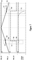
- Figure 7 is graph 700 illustrating leakage current of power detection circuit 100, in some embodiments of the disclosure.
- graph 700 includes a first plot 702 representing the input signal, a second plot 704 representing the reference signal, third plot 706 representing the PWR_RDY signal (represented by a dashed line), fourth plot 708 representing the leakage current (represented by a dashed line), a fifth plot 710 representing the PWR_RDY signal of a conventional power detection circuit (represented by a solid line), and a sixth plot 712 representing leakage current in the conventional power detection circuit (represented by a solid line).
- PWR_RDY signal changes from a first logic value (for example, a logic value zero) to a second logic value (for example a logic value one) when the input signal attains the first threshold (represented as vtripr 208).
- the PWR_RDY signal changes from the second logic value (for example, a logic value one) to the first logic value (for example, a logic value zero) when the input signal drops below the second threshold (represented as vtripf 210) subsequent to attaining the first threshold.
- the leakage current (represented by fourth plot 708) remains constant and does not vary with the change in the input voltage compared to a sharp increase in the leakage current of the conventional power detection circuit (represented by sixth plot 712).
- an increase in the leakage current is limited in the vicinity of power-on region 502 and power-off region 602.
- the increase is limited compared to a sharp increase in the conventional power detection circuit (as shown in sixth plot 712).
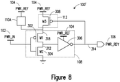
- FIG 8 is a partial block diagram and a partial circuit diagram of a first alternative power detection circuit 100', in accordance with some embodiments.
- first alternative power detection circuit 100' includes first current limiting circuit 110A.
- first alternative power detection circuit 100' includes first transistor M1 302, second transistor M2 304, third transistor M3 308, and inverter 306.
- First transistor M1 302, second transistor M2 304, and inverter 306 form comparator circuit 108.
- Third transistor M3 308 forms feedback circuit 112 which is connected in parallel to first current limiting circuit 110A.
- gate of third transistor M3 308 is connected to second node 314, source/drain of third transistor M3 308 is connected to PWR_REF 104, and drain/source of third transistor M3 308 is connected to fourth node 318.
- First current limiting circuit 110A is connected between fourth node 318 and PWR_REF 104, and is operative to limit the leakage current of comparator circuit 108 via PWR_REF 104.
- first alternative power detection circuit 100' described with reference to Figure 8 is operative to limit the leakage current when a value of the input signal is greater than the second threshold value (that is, vtripf 210).
- FIG. 9 is a partial block diagram and a partial circuit diagram of a second alternative power detection circuit 100", in accordance with some embodiments.
- second alternative power detection circuit 100 includes second current limiting circuit 110B.
- first alternative power detection circuit 100' includes first transistor M1 302, second transistor M2 304, third transistor M3 308, and inverter 306.
- First transistor M1 302, second transistor M2 304, and inverter 306 form comparator circuit 108.
- Third transistor M3 308 forms feedback circuit 112 which is connected in parallel to second current limiting circuit 110B.
- gate of third transistor M3 308 is connected to second node 314, source/drain of third transistor M3 308 is connected to third node 316, and drain/source of third transistor M3 308 is connected to the ground.
- Second current limiting circuit 110B is connected between third node 316 and the ground, and is operative to limit the leakage current of comparator circuit 108 via the ground.
- second alternative power detection circuit 100 described with reference to Figure 9 is operative to limit the leakage current when a value of the input signal is less than the first threshold value (that is, vtripr 208).
- Figure 10 is a flow diagram illustrating a method 1000 for detecting an input power in a circuit, in accordance with some embodiments.
- method 100 can be implemented in power detection circuits 100, 100' and 100" described with reference to Figures 1 , 3 , 4 , 5B , 6B , 8 , and 9 .
- Method 1000 may be performed by a processor.
- method 1000 may be stored as instructions on a memory device, which when executed by a processor can cause the processor to perform method 1000.
- an output signal is provided in response to an input signal through a comparator circuit.
- the PWR_IN signal is received at comparator 108 of power detection circuit 100 and is compared with a first threshold value (that is, vtripr 208).
- the PWR_RDY signal is provided by comparator circuit 108 in response to comparing the PWR_IN signal with the first threshold value (that is, vtripr 208).
- providing the output signal in response to the input signal includes providing the PWR_RDY signal having a first logic value (that is, a logic value one) in response to the PWR_IN signal attaining the first threshold value (that is, vtripr 208) and providing the PWR_RDY signal comprising a second logic value (that is, a logic value zero) when the PWR_IN signal attains the second threshold value (that is, vtripf 210) subsequent to attaining the first threshold value (that is, vtripr 208).
- the second logic value is different than the first logic value.
- the first threshold value (that is, vtripr 208) and the second threshold value (that is, vtripf 210) are controlled.
- each of the first threshold (that is, vtripr 208) and the second threshold (that is, vtripf 210) is controlled by controlling a width, a type of material, or other intrinsic properties of one or more of first transistor M1 302, second transistor M2 304, third transistor M3 308, fourth transistor M4 402A, and fifth transistor M5 402B.
- a leakage current of the comparator circuit is limited through a current limiting circuit.
- the leakage current of comparator circuit 108 is limited through current limiting circuit 110 (that is, one or both of first current limiting circuit 110A and second current limiting circuit 110B).
- Current limiting circuit 110 is connected to comparator 108 and is also connected in parallel to feedback circuit 112.
- power detection circuit 100 described herein can be used for managing power in an associated device or circuit. Moreover, power detection circuit 100 prevent or limit power leakage from an associated device or circuit. For example, power detection circuit 100 can limit or reduce standby power leakage when the input voltage is near the trip point (that is the first threshold value and the second threshold value).
- feedback circuit 112 of power detection circuit 100 provides for the trip point control, that is, control of the first threshold value and the second threshold value. Therefore, power detection circuit 100 provides a different threshold for the power-on and the power-off detection.
- each of the first threshold value and the second threshold value can be altered by altering feedback circuit 112.
- the first threshold value and the second threshold value can be altered by altering characteristics of third transistor M3 306.
- a power detection circuit comprises: a comparator circuit operative to generate an output signal in response to an input signal, wherein the output signal is configured to change from a first value to a second value in response to the input signal attaining a first threshold value, and wherein the output signal is configured to change from the second value to the first value in response to the input signal subsequently attaining a second threshold value; and a current limiting circuit operative to limit a leakage current of the comparator circuit.
- a device comprises a power detection circuit, wherein the power detection circuit comprises: a comparator circuit operative to generate an output signal in response to an input signal, wherein the comparator circuit being operative to generate the output signal comprises the comparator circuit being operative to: provide the output signal comprising a first logic value in response to the input signal attaining a first threshold value, and provide the output signal comprising a second logic value when the input signal subsequently attains a second threshold value, the second logic value being different than the first logic value; a current limiting circuit operative to limit a leakage current of the comparator circuit; and a feedback circuit operative to control the first predetermined threshold and the second predetermined threshold.
- a method of detecting power in a circuit comprises: receiving an input signal at a comparator circuit; comparing, by the comparator circuit, the input signal with a first threshold value; providing, by the comparator circuit, an output signal based on comparing the input signal with the first threshold value, wherein providing the output signal based on comparing the input signal with the first threshold value comprises providing the output signal comprising a first logic value in response to the input signal attaining a first threshold value; comparing, by the comparator circuit, the input signal with a second threshold value subsequent to the input signal attaining the first threshold value; providing, by the comparator circuit, the output signal comprising a second value on response to the input signal attaining the second threshold value subsequent to attaining the first threshold value; controlling the first threshold value and the second threshold value through a feedback circuit, wherein the feedback circuit is connected to the comparator circuit; and limiting a leakage current of the comparator circuit through a current limiting circuit, wherein the current limiting circuit is connected in parallel to the feedback circuit.
Landscapes
- Physics & Mathematics (AREA)
- General Physics & Mathematics (AREA)
- Engineering & Computer Science (AREA)
- Power Engineering (AREA)
- Nonlinear Science (AREA)
- Measurement Of Current Or Voltage (AREA)
- Logic Circuits (AREA)
- Control Of Voltage And Current In General (AREA)
Abstract
A power detection circuit is provided. The power detection circuit includes a comparator circuit operative to generate an output signal in response to an input signal. The output signal is configured to change from a first value to a second value in response to the input signal attaining a first threshold value. The output signal is configured to change from the second value to the first value in response to the input signal subsequently attaining a second threshold value. A current limiting circuit is connected to the comparator circuit and operative to limit a leakage current of the comparator circuit.
Description
- It is often desirable to detect flow of power to a circuit such as in an on-chip power to reduce or prevent interface leakage in a dual power system. For example, a power detector can be configured to detect the voltage level of an input power. When the voltage level is higher than a certain threshold, the power detector outputs a specific logic state to indicate that the power is on. When the voltage is lower than a certain threshold, the power detector outputs another logic state to indicate that the power is off.
- Aspects of the present disclosure are best understood from the following detailed description when read with the accompanying figures. It is noted that, in accordance with the standard practice in the industry, various features are not drawn to scale. In fact, the dimensions of the various features may be arbitrarily increased or reduced for clarity of discussion.
-
Figure 1 is a schematic diagram of a power detection circuit, in accordance with some embodiments. -
Figure 2 is a graph illustrating signals of a power detection circuit, in accordance with some embodiments. -
Figure 3 is a partial block diagram and a partial circuit diagram of a power detection circuit, in accordance with some embodiments. -
Figure 4 is an example circuit diagram of a power detection circuit, in accordance with some embodiments. -
Figures 5A and 5B illustrates power-on detection, in accordance with some embodiments. -
Figures 6A and 6B illustrates power-off detection, in accordance with some embodiments. -
Figure 7 is graph illustrating leakage current of a power detection circuit, in some embodiments of the disclosure. -
Figure 8 is a partial block diagram and a partial circuit diagram of a first alternative power detection circuit, in accordance with some embodiments. -
Figure 9 is a partial block diagram and a partial circuit diagram of a second alternative power detection circuit, in accordance with some embodiments. -
Figure 10 is a flow diagram illustrating a method for detecting an input power in a circuit, in accordance with some embodiments. - The following disclosure provides many different embodiments, or examples, for implementing different features of the provided subject matter. Specific examples of components and arrangements are described below to simplify the present disclosure. These are, of course, merely examples and are not intended to be limiting. For example, the formation of a first feature over or on a second feature in the description that follows may include embodiments in which the first and second features are formed in direct contact, and may also include embodiments in which additional features may be formed between the first and second features, such that the first and second features may not be in direct contact. In addition, the present disclosure may repeat reference numerals and/or letters in the various examples. This repetition is for the purpose of simplicity and clarity and does not in itself dictate a relationship between the various embodiments and/or configurations discussed.
- It will be understood that, although the terms "first," "second," "third," etc., may be used herein to describe various elements, components, regions, layers and/or sections, these elements, components, regions, layers and/or sections should not be limited by these terms. These terms are used to distinguish one element, component, region, layer or section from another element, component, region, layer or section. Thus, a first element, component, region, layer or section described below could be termed a second element, component, region, layer or section, without departing from the spirit and scope of the present invention.
- It will be understood that when an element or layer is referred to as being "on," "connected to," or "coupled to" another element or layer, it can be directly on, connected to, or coupled to the other element or layer, or one or more intervening elements or layers may be present. In addition, it will also be understood that when an element or layer is referred to as being "between" two elements or layers, it can be the only element or layer between the two elements or layers, or one or more intervening elements or layers may also be present.
- There are known techniques for detecting flow of power to the circuit. However, these known techniques suffer from disadvantages such as high leakage of the power. The leakage causes inefficiency and increased power consumption by the circuit.
Figure 1 is a block diagram of a power detection circuit, in accordance with some embodiments.Power detection circuit 100 can be associated with a device or a circuit, and is operative to determine a status of an input voltage or an input power to the associated device or the circuit. For example,power detection circuit 100 is operative to continuously compare a value of the input voltage or the input power with a first threshold value and a second threshold value. Based on the comparison,power detection circuit 100 is operative to provide an output signal with a predetermined value indicating whether the input voltage or the input power above or below the first threshold value and the second threshold value. For example,power detection circuit 100 is operative to provide an output signal having a first logic value in response to determining that the input voltage to the associated circuit or device is more than (or has attained) the first threshold value. In addition,power detection circuit 100 is operative to subsequently provide the output signal having a second logic value in response to determining that the input voltage to the associated circuit or device is lower than (or has attained) the second threshold value subsequent to attaining the first threshold value. That is,power detection circuit 100 is operative to change a value of the output signal from the first logic value to the second logic value in response to the input voltage dropping below the second threshold value subsequent to reaching the first threshold value. - As shown in
Figure 1 ,power detection circuit 100 includes a first input 102 (also referred to as PWR_IN 102). In addition,power detection circuit 100 includes a second input 104 (also referred to as PWR_REF 104). First input 102 (that is, PWR_IN 102) is operative to receive an input signal and second input 104 (that is, PWR_REF 104) is operative to receive a reference signal. The input signal is representative of the input voltage or the input power being provided to the associated device or circuit. The reference signal is representative of a supply voltage (also referred to as a supply power or a reference voltage) being applied to the associated device or circuit. In some embodiments, the input signal is also referred to as a PWR_IN signal and the output signal is referred to as a PWR_RDY signal. Althoughpower detection circuit 100 ofFigure 1 is shown to include only one supply voltage input (that is, PWR REF 104), it will be apparent to a person with ordinary skill in the art thatpower detection circuit 100 may include more than one supply voltage inputs. - Continuing with
Figure 1 ,power detection circuit 100 further includes acomparator circuit 108, a current limitingcircuit 110, and afeedback circuit 112.Comparator circuit 108 is operative to generate the output signal (that is, the PWR_RDY signal) responsive to the input signal (that is, the PWR_IN signal). For example,comparator circuit 108 is operative to continuously compare a value of the input signal with the first threshold value and the second threshold value. In example embodiments, each of the first threshold value and the second threshold value can be based on the PWR_REF signal. For example, the first threshold value can be 0.5 times a voltage of the PWR_REF signal and the second threshold value can be 0.3 times a value of the PWR_REF signal. -
Comparator circuit 108 is further operative to generate, based on the comparison, the output signal having a first logic value (that is, a logic value one or a logic value zero) in response to the input signal attaining the first threshold value, and provide the output signal having a second logic value (that is, a logic value zero or a logic value one), when the input signal subsequently attains the second threshold value.Comparator circuit 108 includes one or more transistors. In example embodiments, transistors ofcomparator circuit 108 may each include a metal oxide semiconductor field effect transistor, an n-channel metal oxide semiconductor transistor, a p-channel metal oxide semiconductor transistor, or a complementary metal oxide semiconductor transistor. However, other types of transistors are within the scope of the disclosure. - Current limiting
circuit 110 is connected betweencomparator circuit 108 and the supply voltage. In addition, current limitingcircuit 110 can also be connected betweencomparator circuit 108 and the ground. Current limitingcircuit 110 is operative to limit a leakage current ofcomparator circuit 108. For example, current limitingcircuit 110 is operative to limit the leakage current of the one or more transistors ofcomparator circuit 108. Current limitingcircuit 110 includes one or more resistors or transistors. In example embodiments, transistors of current limitingcircuit 110 may include a metal oxide semiconductor field effect transistor, an n-channel metal oxide semiconductor transistor, a p-channel metal oxide semiconductor transistor, and a complementary metal oxide semiconductor transistor. In addition, it will be apparent a person with skill in the art after reading this disclosure that other types of transistors are within the scope of the disclosure. -
Feedback circuit 112 is connected tocomparator circuit 108. In some examples, feedback circuit is connected in parallel to current limitingcircuit 110.Feedback circuit 112 is operative to control one or both of the first threshold value and the second threshold value associated withcomparator circuit 108.Feedback circuit 112 includes one or more transistors. In example embodiments, transistors offeedback circuit 112 may include a metal oxide semiconductor field effect transistor, an n-channel metal oxide semiconductor transistor, a p-channel metal oxide semiconductor transistor, and a complementary metal oxide semiconductor transistor. However, other types of transistors are within the scope of the disclosure. -
Figure 2 is agraph 200 illustrating plots of the input signal and the output signal ofpower detection circuit 100, in accordance with some embodiments. As shown inFigure 2 ,graph 200 includes afirst plot 202 representing the input signal (that is, the PWR_IN signal), asecond plot 204 representing the reference signal (that is, the PWR_REF signal), and athird plot 206 representing the output signal (that is, the PWR_RDY signal). - As illustrated in
first plot 210 andthird plot 206 ofgraph 200, when a value of the input signal (that is, the PWR_IN signal) crosses the first threshold value (also referred to as vtripr 208), a value of the output signal (that is, the PWR_RDY signal) changes from a first logic value to a second logic value (that is, from a logic value zero to a logic value one), and remains at the second logic as long as the value of the PWR_IN signal remains above the second threshold value (also referred to as vtripf 210). However, when the value of the PWR_IN signal subsequently attains (or drop below) the second threshold value (that is, vtripf 210), the value of the PWR_RDY signal changes from the second logic value to the first logic value (that is, from a logic value one to a logic value zero). - In some embodiments, the first threshold value (that is, vtripr 208) and the second threshold value (that is, vtripf 210) is predetermined. For example, each of the first threshold value (that is, vtripr 208) and the second threshold value (that is, vtripf 210) is predetermined by a user or by design of
power detection circuit 100. Moreover, the first threshold value (that is, vtripr 208) can be different than the second threshold (that is, vtripf 210). For example, the first threshold value (that is, vtripr 208) is higher than the second threshold value (that is, vtripf 210). In example embodiments, the first threshold value can be a minimum voltage required to switch-on components of the device or circuit associated withpower detection circuit 100. In addition, the second threshold value can be a minimum voltage required for the components of the device or circuit associated withpower detection circuit 100 to remain switched on. In some embodiments, each of the first threshold value (that is, vtripr 208) and the second threshold value (that is, vtripf 210) is dynamically configured. -
Figure 3 is a partial block diagram and a partial circuit diagram ofpower detection circuit 100, in accordance with some embodiments. As shown inFigure 3 ,power detection circuit 100 includescomparator circuit 108, a first current limitingcircuit 110A, a second current limitingcircuit 110B, and afeedback circuit 112. Althoughpower detection circuit 100 ofFigure 3 is shown to include two current limiting circuits (that is, first current limitingcircuit 110A and second current limitingcircuit 110B), it will be apparent to a person skilled in the art after reading this disclosure thatpower detection circuit 100 may include only one current limitingcircuit 110 or more than two current limiting circuits. In addition,power detection circuit 100 includes a first input 102 (that is, PWR_IN 102) and second inputs 104 (that is, PWR_REF 104). -
Comparator circuit 108 is operative to determine a value of the input signal (that is, the PWR_IN signal) and provide the output signal (that is, the PWR_RDY signal) by comparing the determined value with a plurality of threshold values (for example, the first threshold value (that is, vtripr 208) and the second threshold value (that is, vtripf 210)). As shown inFigure 3 ,comparator circuit 108 includes afirst transistor M1 302, asecond transistor M2 304, and aninverter 306.First transistor M1 302 can be a pMOS transistor andsecond transistor M2 304 can be an nMOS transistor. However, it will be apparent to a person with ordinary skill in the art after reading this disclosure that other types of transistors are within the scope of the disclosure. -
Inverter 306 is a NOT logic gate. However, it will be apparent to a person with ordinary skill in the art after reading this disclosure that other types of inverters are within the scope of the disclosure.Feedback circuit 112 includes athird transistor M3 308.Third transistor M3 308 can be an nMOS transistor. However, it will be apparent to a person with ordinary skill in the art after reading this disclosure that other types of transistors are within the scope of the disclosure. - A drain/source of
first transistor M1 302 is connected to a source/drain ofsecond transistor M2 304 at afirst node 312. In addition, an input ofinverter 306 is connected tofirst node 312. An output ofinverter 306 is connected to asecond node 314. Output ofinverter 306 is also an output ofcomparator circuit 108 andpower detection circuit 100. The output ofcomparator circuit 108 is provided atPWR_RDY 106 as the output signal. - Continuing with
Figure 3 , a drain/source ofsecond transistor M2 304 is connected to athird node 316. Moreover, a source/drain ofthird transistor M3 308 is also connected tothird node 316. In addition, a first terminal of second current limitingcircuit 110B is connected tothird node 316. A second terminal of second current limitingcircuit 110B is connected to the ground. In addition, a drain/source ofthird transistor M3 308 is also connected to the ground. Thus,third transistor M3 308 is connected in parallel to second current limitingcircuit 110B. Therefore, second current limitingcircuit 110B is connected in parallel tofeedback circuit 112. - Still continuing with
Figure 3 , a source drain offirst transistor 302 is connected to afourth node 318. In addition, a second terminal of first current limitingcircuit 110A is connected tofourth node 318. Moreover, a first terminal of first current limitingcircuit 110A is connected to the supply voltage (that is, PWR_REF 104). Hence, first current limitingcircuit 110A is connected between the supply voltage andcomparator circuit 108. As will be discussed further below, first current limitingcircuit 110A is operative to control or limit a leakage current ofcomparator circuit 108 throughPWR_REF 104. - A first terminal of second current limiting
circuit 110B is connected tothird node 316 and a second terminal of second current limitingcircuit 110B is connected to the ground. Hence, second current limitingcircuit 110B is connected betweencomparator circuit 108 and the ground. Thus, second current limitingcircuit 110B is operative to control or limit a leakage current ofcomparator circuit 108 to the ground. -
Figure 4 is an example circuit diagram ofpower detection circuit 100 in accordance with some embodiments. As shown inFigure 4 , first current limitingcircuit 110A includes afourth transistor M4 402A and second current limitingcircuit 110B includes afifth transistor M5 402B. Each offourth transistor M4 402A of first current limitingcircuit 110A andfifth transistor M5 402B of second current limitingcircuit 110B is an nMOS transistor. However, it will be apparent to a person with ordinary skill in the art after reading this disclosure that other types of transistors are within the scope of the disclosure. - Continuing with
Figure 4 , a source/drain offourth transistor M4 402A of first current limitingcircuit 110A is connected to PWR_REF 104 (that is, the supply voltage). Moreover, a gate offourth transistor M4 402A is also connected to PWR_REF 104 (that is, the supply voltage). In addition, a drain/source offourth transistor M4 402A is connected tofourth node 318. Hence,fourth transistor M4 402A is connected between the supply voltage andcomparator circuit 108. In operation,fourth transistor M4 402A is operative to control or limit a leakage current ofcomparator circuit 108 throughPWR_REF 104. - A source/drain of
fifth transistor M5 402B is connectedthird node 316. Moreover, a gate offifth transistor M5 402B is also connected tothird node 316. In addition, a drain/source offifth transistor M5 402B is connected to the ground. Hence,fifth transistor M5 402B is connected betweencomparator circuit 108 and the ground. In operation,fifth transistor M5 402B is operative to control or limit a leakage current ofcomparator circuit 108 to the ground. -
Figures 5A and 5B illustrates power-on detection, in accordance with some embodiments. A power-onregion 502 of the input signal is shown inFigure 5A . As shown inFigure 5A , power-onregion 502 represents a region which is in vicinity of the first threshold value (that is, vtripr 208) offirst plot 202 representing the input signal (that is, the input voltage or the input power). In example embodiments, a value of the input signal (represented by first plot 202) in power-onregion 502 is less than the first threshold value (that is, vtripr 208) but is sufficient to switch-onfirst transistor M1 302 andsecond transistor M2 304 ofcomparator circuit 108. - In example embodiments, since a value of the input signal (represented by first plot 202) in power-on
region 502 is less than the first threshold value (that is, vtripr 208), the value of the output signal ofpower detection circuit 100 is at a logic value zero. Hence,second node 314 ofpower detection circuit 100 is at a logic value zero. Sincesecond node 314 is at a logic value zero,first node 312 ofpower detection circuit 100 is at a logic value one. In addition, in power-onregion 502, a value of the input signal is still not enough to switch-onsecond transistor M2 304 ofcomparator circuit 108. Therefore,second transistor M2 304 ofcomparator circuit 108 is still switched-off. However, in power-onregion 502,first transistor M1 302 ofcomparator circuit 108 is switched-on. In addition, sincesecond node 314 is at a logic value zero,third transistor M3 308 offeedback circuit 112 ofpower detection circuit 100 is disconnected from power detection circuit 100 (the disconnection being represented by dashed lines). - Moreover, in power-on
region 502, since,second transistor M2 304 ofcomparator circuit 108 is switched-off,fifth transistor M5 402B of second current limitingcircuit 110B is also switched-off, thereby limiting the leakage current fromcomparator circuit 108 to the ground. In addition, althoughfourth transistor M4 402A of first current limitingcircuit 110A is switched-on, the first terminal offourth transistor M4 402A is connected to the supply voltage which is higher than the input voltage, thereby limiting the leakage current fromcomparator circuit 108 to the supply voltage. Therefore, the first threshold value is determined by one or more offirst transistor M1 302,second transistor M2 304,fourth transistor M4 402A, andfifth transistor 402B. For example, the first threshold value is determined by a width, a type of material, or other intrinsic properties of one or more offirst transistor M1 302,second transistor M2 304,fourth transistor M4 402A, andfifth transistor M5 402B. - For example, a current through
fourth transistor M4 402A is provided as:
first transistor M1 302 is provided as:
second transistor M2 304 is provided as:
fifth transistor M5 402B is provided as:
fourth node 318, Vy is a voltage offirst node 312, and V0 is a voltage ofthird node 316. - In
Figure 5B , IM4 is equal to IM1 which is equal to IM2 which is equal to IM5. That is:
first transistor M1 302,second transistor M2 304,fourth transistor M4 402A, andfifth transistor M5 402B. In addition, Vo is assumed to be equal to 0.5(VPWR_REP). Hence, from equations (1), (2), (3), (4), and (5):


first transistor M1 302,second transistor M2 304,fourth transistor M4 402A, andfifth transistor M5 402B. -
Figures 6A and 6B illustrates power-off detection, in accordance with some embodiments. A power-off region 602 of the input signal is shown inFigure 6A . As shown inFigure 6A , power-off region 602 represents a region which is in vicinity of the second threshold value (that is, vtripf 210) offirst plot 202 representing the input signal (that is, the input voltage or the input power). In example embodiments, a value of the input signal (represented by first plot 202) in power-off region 602 is more than the second threshold value (that is, vtripf 210) and less than the first threshold (that is, vtripr 208) but is not sufficient to switch-offsecond transistor M2 304 ofcomparator circuit 108. - In example embodiments, even though lower than the first threshold value, a value of the input signal (represented by first plot 202) in power-
off region 602 is still more than the second threshold value (that is, vtripf 210), the value of the output signal ofpower detection circuit 100 is still at a logic value one. Hence,second node 314 ofpower detection circuit 100 is still at a logic value one. Sincesecond node 314 is at a logic value one,first node 312 ofpower detection circuit 100 is at a logic value zero. In addition, although lower than the first threshold value (vtripr 208), a value of the input signal in switch-off region 602 is still not low enough to switch-offsecond transistor M2 304 ofcomparator circuit 108. Therefore, in power-off region 602,first transistor M1 302 ofcomparator circuit 108 is switched-off andsecond transistor M2 304 ofcomparator circuit 108 is switched-on. In addition,fourth transistor M4 402A of first current limitingcircuit 110A is also switched-off thereby limiting the leakage current ofcomparator circuit 108 throughPWR_REF 104. For example, when the input signal (represented by first plot 202) is near a threshold value ofpower detection circuit 100,first transistor M1 302 andsecond transistor M2 304 may be simultaneously switched-on thereby creating a leakage path. By adding current limitingcircuit 110, a bias voltage (Vgs) offirst transistor M1 302 and a bias voltage (Vgs) ofsecond transistor M2 304 is reduced due to a voltage drop created by current limitingcircuit 110. Therefore, the leakage current is reduced according to a saturation current equation Id = 1/2 K(Vgs-Vt)^2, where Vt is a threshold voltage forfirst transistor M1 302 andsecond transistor M2 304. - In addition, in power-
off region 602, since,second node 314 is at a logic value one,third transistor M3 308 offeedback circuit 112 ofpower detection circuit 100 is switched-on. Moreover, sincethird transistor M3 308 is switched-on,third node 316 is at a logic value zero. Therefore,fifth transistor M5 402B of second current limitingcircuit 110B is disconnected from power detection circuit 100 (the disconnection represented by dashed lines). In addition, the second threshold value (that is, vtripf 210) is determined by one or more offirst transistor M1 302,second transistor M2 304,third transistor M3 308, andfourth transistor M4 402A. For example, the second threshold value is determined by a width, a type of material, or other intrinsic properties of one or more offirst transistor M1 302,second transistor M2 304,third transistor M3 308, andfourth transistor M4 402A. - For example, a current through
fourth transistor M4 402A is provided as:
first transistor M1 302 is provided as:
second transistor M2 304 is provided as:
third transistor M3 308 whish can be assumed to operate in a linear mode, is provided as:
- In
Figure 6B , IM4 is equal to IM1 which is equal to IM2 which is equal to IM5. That is:
first transistor M1 302,second transistor M2 304,fourth transistor M4 402A, andthird transistor M3 308. In addition, Vo is assumed to be equal to 0.5(VPWR_REP) and Vy is equal to 0. Hence, from equations (6), (7), (8), (9), and (10):

first transistor M1 302,second transistor M2 304,fourth transistor M4 402A, andthird transistor M3 308. -
Figure 7 is graph 700 illustrating leakage current ofpower detection circuit 100, in some embodiments of the disclosure. As shown inFigure 7 , graph 700 includes afirst plot 702 representing the input signal, asecond plot 704 representing the reference signal,third plot 706 representing the PWR_RDY signal (represented by a dashed line),fourth plot 708 representing the leakage current (represented by a dashed line), afifth plot 710 representing the PWR_RDY signal of a conventional power detection circuit (represented by a solid line), and asixth plot 712 representing leakage current in the conventional power detection circuit (represented by a solid line). As shown byfirst plot 702 andthird plot 706 of graph 700, PWR_RDY signal changes from a first logic value (for example, a logic value zero) to a second logic value (for example a logic value one) when the input signal attains the first threshold (represented as vtripr 208). In addition, and as shown byfirst plot 702 andthird plot 706 graph 700, the PWR_RDY signal changes from the second logic value (for example, a logic value one) to the first logic value (for example, a logic value zero) when the input signal drops below the second threshold (represented as vtripf 210) subsequent to attaining the first threshold. - Continuing with
Figure 7 , the leakage current (represented by fourth plot 708) remains constant and does not vary with the change in the input voltage compared to a sharp increase in the leakage current of the conventional power detection circuit (represented by sixth plot 712). In addition, and as shown infourth plot 708, an increase in the leakage current is limited in the vicinity of power-onregion 502 and power-off region 602. However, the increase is limited compared to a sharp increase in the conventional power detection circuit (as shown in sixth plot 712). -
Figure 8 is a partial block diagram and a partial circuit diagram of a first alternative power detection circuit 100', in accordance with some embodiments. As shown inFigure 8 , first alternative power detection circuit 100' includes first current limitingcircuit 110A. In addition, first alternative power detection circuit 100' includesfirst transistor M1 302,second transistor M2 304,third transistor M3 308, andinverter 306.First transistor M1 302,second transistor M2 304, andinverter 306form comparator circuit 108.Third transistor M3 308forms feedback circuit 112 which is connected in parallel to first current limitingcircuit 110A. For example, gate ofthird transistor M3 308 is connected tosecond node 314, source/drain ofthird transistor M3 308 is connected toPWR_REF 104, and drain/source ofthird transistor M3 308 is connected tofourth node 318. First current limitingcircuit 110A is connected betweenfourth node 318 andPWR_REF 104, and is operative to limit the leakage current ofcomparator circuit 108 viaPWR_REF 104. - During operation, when a value of the input signal is less that the first threshold value (that is, vtripr 208), the value of the output signal of
comparator circuit 108 is at a logic value zero. In addition, when a value of the input signal is less than the first threshold value (that is, vtripr 208),third transistor M3 308 is switched-on and first current limitingcircuit 110A is bypassed. However, when a value of the input signal is greater than the second threshold value (that is, vtripf 210),third transistor M3 308 is switched-off and the leakage current is limited by first current limitingcircuit 110A. Hence, and in accordance with example embodiments, first alternative power detection circuit 100' described with reference toFigure 8 is operative to limit the leakage current when a value of the input signal is greater than the second threshold value (that is, vtripf 210). -
Figure 9 is a partial block diagram and a partial circuit diagram of a second alternativepower detection circuit 100", in accordance with some embodiments. As shown inFigure 9 , second alternativepower detection circuit 100" includes second current limitingcircuit 110B. In addition, first alternative power detection circuit 100' includesfirst transistor M1 302,second transistor M2 304,third transistor M3 308, andinverter 306.First transistor M1 302,second transistor M2 304, andinverter 306form comparator circuit 108.Third transistor M3 308forms feedback circuit 112 which is connected in parallel to second current limitingcircuit 110B. For example, gate ofthird transistor M3 308 is connected tosecond node 314, source/drain ofthird transistor M3 308 is connected tothird node 316, and drain/source ofthird transistor M3 308 is connected to the ground. Second current limitingcircuit 110B is connected betweenthird node 316 and the ground, and is operative to limit the leakage current ofcomparator circuit 108 via the ground. - During operation, when a value of the input signal is less that the first threshold value (that is, vtripr 208), the value of the output signal of
comparator circuit 108 is at a logic value zero. In addition, when a value of the input signal is less that the first threshold value (that is, vtripr 208),third transistor M3 308 is switched-off. Hence, the leakage current is limit by second current limitingcircuit 110B. However, when a value of the input signal is greater than the second threshold (that is, vtripf 210),third transistor M3 308 is switched-on and second current limitingcircuit 110B is bypassed. Hence, and in accordance with example embodiments, second alternativepower detection circuit 100" described with reference toFigure 9 is operative to limit the leakage current when a value of the input signal is less than the first threshold value (that is, vtripr 208). -
Figure 10 is a flow diagram illustrating amethod 1000 for detecting an input power in a circuit, in accordance with some embodiments. For example,method 100 can be implemented inpower detection circuits Figures 1 ,3 ,4 ,5B ,6B ,8 , and9 .Method 1000 may be performed by a processor. In addition,method 1000 may be stored as instructions on a memory device, which when executed by a processor can cause the processor to performmethod 1000. - At
block 1010 ofmethod 1000, an output signal is provided in response to an input signal through a comparator circuit. For example, the PWR_IN signal is received atcomparator 108 ofpower detection circuit 100 and is compared with a first threshold value (that is, vtripr 208). The PWR_RDY signal is provided bycomparator circuit 108 in response to comparing the PWR_IN signal with the first threshold value (that is, vtripr 208). For example, providing the output signal in response to the input signal includes providing the PWR_RDY signal having a first logic value (that is, a logic value one) in response to the PWR_IN signal attaining the first threshold value (that is, vtripr 208) and providing the PWR_RDY signal comprising a second logic value (that is, a logic value zero) when the PWR_IN signal attains the second threshold value (that is, vtripf 210) subsequent to attaining the first threshold value (that is, vtripr 208). The second logic value is different than the first logic value. - At
block 1020 ofmethod 1000, the first threshold value (that is, vtripr 208) and the second threshold value (that is, vtripf 210) are controlled. For example, , each of the first threshold (that is, vtripr 208) and the second threshold (that is, vtripf 210) is controlled by controlling a width, a type of material, or other intrinsic properties of one or more offirst transistor M1 302,second transistor M2 304,third transistor M3 308,fourth transistor M4 402A, andfifth transistor M5 402B. - At
block 1030 ofmethod 1000, a leakage current of the comparator circuit is limited through a current limiting circuit. For example, the leakage current ofcomparator circuit 108 is limited through current limiting circuit 110 (that is, one or both of first current limitingcircuit 110A and second current limitingcircuit 110B). Current limitingcircuit 110 is connected tocomparator 108 and is also connected in parallel tofeedback circuit 112. - In example embodiments,
power detection circuit 100 described herein can be used for managing power in an associated device or circuit. Moreover,power detection circuit 100 prevent or limit power leakage from an associated device or circuit. For example,power detection circuit 100 can limit or reduce standby power leakage when the input voltage is near the trip point (that is the first threshold value and the second threshold value). In addition,feedback circuit 112 ofpower detection circuit 100 provides for the trip point control, that is, control of the first threshold value and the second threshold value. Therefore,power detection circuit 100 provides a different threshold for the power-on and the power-off detection. Moreover, each of the first threshold value and the second threshold value can be altered by alteringfeedback circuit 112. For example, the first threshold value and the second threshold value can be altered by altering characteristics ofthird transistor M3 306. - In accordance with example embodiments, a power detection circuit comprises: a comparator circuit operative to generate an output signal in response to an input signal, wherein the output signal is configured to change from a first value to a second value in response to the input signal attaining a first threshold value, and wherein the output signal is configured to change from the second value to the first value in response to the input signal subsequently attaining a second threshold value; and a current limiting circuit operative to limit a leakage current of the comparator circuit.
- In example embodiments, a device comprises a power detection circuit, wherein the power detection circuit comprises: a comparator circuit operative to generate an output signal in response to an input signal, wherein the comparator circuit being operative to generate the output signal comprises the comparator circuit being operative to: provide the output signal comprising a first logic value in response to the input signal attaining a first threshold value, and provide the output signal comprising a second logic value when the input signal subsequently attains a second threshold value, the second logic value being different than the first logic value; a current limiting circuit operative to limit a leakage current of the comparator circuit; and a feedback circuit operative to control the first predetermined threshold and the second predetermined threshold.
- In accordance with example embodiments, a method of detecting power in a circuit comprises: receiving an input signal at a comparator circuit; comparing, by the comparator circuit, the input signal with a first threshold value; providing, by the comparator circuit, an output signal based on comparing the input signal with the first threshold value, wherein providing the output signal based on comparing the input signal with the first threshold value comprises providing the output signal comprising a first logic value in response to the input signal attaining a first threshold value; comparing, by the comparator circuit, the input signal with a second threshold value subsequent to the input signal attaining the first threshold value; providing, by the comparator circuit, the output signal comprising a second value on response to the input signal attaining the second threshold value subsequent to attaining the first threshold value; controlling the first threshold value and the second threshold value through a feedback circuit, wherein the feedback circuit is connected to the comparator circuit; and limiting a leakage current of the comparator circuit through a current limiting circuit, wherein the current limiting circuit is connected in parallel to the feedback circuit.
- The foregoing outlines features of several embodiments so that those skilled in the art may better understand the aspects of the present disclosure. Those skilled in the art should appreciate that they may readily use the present disclosure as a basis for designing or modifying other processes and structures for carrying out the same purposes and/or achieving the same advantages of the embodiments introduced herein. Those skilled in the art should also realize that such equivalent constructions do not depart from the spirit and scope of the present disclosure, and that they may make various changes, substitutions, and alterations herein without departing from the spirit and scope of the present disclosure.
Claims (10)
- A power detection circuit comprising:a comparator circuit operative to generate an output signal in response to an input signal, wherein the output signal is configured to change from a first value to a second value in response to the input signal attaining a first threshold value, and wherein the output signal is configured to change from the second value to the first value in response to the input signal subsequently attaining a second threshold value; anda current limiting circuit connected to the comparator circuit and operative to limit a leakage current of the comparator circuit.
- The power detection circuit of claim 1, further comprising a feedback circuit connected to the comparator circuit and operative to control the first threshold value and the second threshold value.
- The power detection circuit of claim 2, wherein the comparator circuit comprises a first transistor, a second transistor, and an inverter, wherein gates of each of the first transistor and the second transistor are connected to the input signal, wherein a drain/source of the first transistor is connected to the source/drain of the second transistor at a first node, wherein an input of the inverter is connected to the first node, and wherein an output of the inverter is operative to provide the output signal at a second node.
- The power detection circuit of claim 3, wherein the first transistor is an n-channel metal oxide semiconductor transistor, and wherein the second transistor is a p-channel metal oxide semiconductor transistor.
- The power detection circuit of claim 3, wherein the feedback circuit is connected to the second node.
- The power detection circuit of claim 3, wherein the feedback circuit comprises a third transistor, wherein a gate of the third transistor is connected to the second node, wherein a source/drain on the third transistor is connected to a third node, and wherein a drain/source of the third transistor is connected to the ground.
- The power detection circuit of claim 6, wherein the current limiting circuit comprises a fourth transistor, wherein a gate of the fourth transistor is connected to the third node, wherein a source/drain on the fourth transistor is connected to the third node, and wherein a drain/source of the fourth transistor is connected to the ground.
- The power detection circuit of claim 7, wherein the current limiting circuit further comprises a fifth transistor, wherein a gate of the fifth transistor is connected to a supply voltage, wherein a source/drain on the fifth transistor is connected to the supply voltage, and wherein a drain/source of the fifth transistor is connected to a fourth node.
- The power detection circuit of claim 7, wherein a source/drain of the first transistor is connected to the fourth node.
- The power detection circuit of claim 7, wherein a drain/source of the second transistor is connected to the third node.
Applications Claiming Priority (1)
| Application Number | Priority Date | Filing Date | Title |
|---|---|---|---|
| US16/935,608 US11598794B2 (en) | 2020-07-22 | 2020-07-22 | Power detection circuit |
Publications (1)
| Publication Number | Publication Date |
|---|---|
| EP3943953A1 true EP3943953A1 (en) | 2022-01-26 |
Family
ID=77021082
Family Applications (1)
| Application Number | Title | Priority Date | Filing Date |
|---|---|---|---|
| EP21186834.4A Withdrawn EP3943953A1 (en) | 2020-07-22 | 2021-07-21 | Power detection circuit |
Country Status (5)
| Country | Link |
|---|---|
| US (4) | US11598794B2 (en) |
| EP (1) | EP3943953A1 (en) |
| JP (1) | JP2022022176A (en) |
| CN (1) | CN113630109B (en) |
| TW (1) | TWI778488B (en) |
Families Citing this family (2)
| Publication number | Priority date | Publication date | Assignee | Title |
|---|---|---|---|---|
| US11598794B2 (en) * | 2020-07-22 | 2023-03-07 | Taiwan Semiconductor Manufacturing Company, Ltd. | Power detection circuit |
| US11451310B1 (en) * | 2021-03-19 | 2022-09-20 | Qualcomm Incorporated | RF power detector |
Citations (1)
| Publication number | Priority date | Publication date | Assignee | Title |
|---|---|---|---|---|
| US20140077842A1 (en) * | 2012-09-14 | 2014-03-20 | Nxp B.V. | Zero or ultra-low dc current consumption power-on and brown-out detector |
Family Cites Families (11)
| Publication number | Priority date | Publication date | Assignee | Title |
|---|---|---|---|---|
| DE60320314T2 (en) | 2003-02-20 | 2009-06-25 | International Business Machines Corp. | TEST PROCEDURES FOR INTEGRATED CIRCUITS WITH USE MODIFICATION OF WELL VOLTAGES |
| US6992489B2 (en) * | 2004-02-11 | 2006-01-31 | Agere Systems Inc. | Multiple voltage level detection circuit |
| US7075373B2 (en) * | 2004-11-02 | 2006-07-11 | Micrel, Inc. | Overcurrent protection circuit with fast current limiting control |
| US7733155B2 (en) * | 2005-06-06 | 2010-06-08 | Semiconductor Components Industries, Llc | Low power voltage detection circuit and method therefor |
| US8022734B1 (en) * | 2008-08-25 | 2011-09-20 | Peregrine Semiconductor Corporation | Low current power detection circuit providing window comparator functionality |
| CN106026619B (en) * | 2016-06-24 | 2019-03-22 | 成都芯源系统有限公司 | Current-limiting peak value adjusting circuit, current-limiting unit, control circuit and power converter |
| CN106712513B (en) * | 2017-01-11 | 2023-10-13 | 北京集创北方科技股份有限公司 | Peak current detection circuit and power conversion device |
| US10804691B2 (en) * | 2018-03-06 | 2020-10-13 | Texas Instruments Incorporated | Circuit providing reverse current protection for high-side driver |
| US10620676B1 (en) * | 2018-10-11 | 2020-04-14 | Analog Devices Global Unlimited Company | Wake-up control circuit for power-gated integrated circuits |
| TWI684770B (en) | 2019-03-28 | 2020-02-11 | 高苑科技大學 | DC power supply leakage current detection device |
| US11598794B2 (en) * | 2020-07-22 | 2023-03-07 | Taiwan Semiconductor Manufacturing Company, Ltd. | Power detection circuit |
-
2020
- 2020-07-22 US US16/935,608 patent/US11598794B2/en active Active
-
2021
- 2021-01-05 TW TW110100247A patent/TWI778488B/en active
- 2021-03-01 CN CN202110227719.9A patent/CN113630109B/en active Active
- 2021-07-21 JP JP2021120458A patent/JP2022022176A/en active Pending
- 2021-07-21 EP EP21186834.4A patent/EP3943953A1/en not_active Withdrawn
-
2023
- 2023-03-06 US US18/178,900 patent/US11913980B2/en active Active
-
2024
- 2024-02-26 US US18/587,508 patent/US12298331B2/en active Active
-
2025
- 2025-05-12 US US19/205,621 patent/US20250341552A1/en active Pending
Patent Citations (1)
| Publication number | Priority date | Publication date | Assignee | Title |
|---|---|---|---|---|
| US20140077842A1 (en) * | 2012-09-14 | 2014-03-20 | Nxp B.V. | Zero or ultra-low dc current consumption power-on and brown-out detector |
Also Published As
| Publication number | Publication date |
|---|---|
| CN113630109A (en) | 2021-11-09 |
| TWI778488B (en) | 2022-09-21 |
| US11913980B2 (en) | 2024-02-27 |
| US12298331B2 (en) | 2025-05-13 |
| CN113630109B (en) | 2025-07-22 |
| US11598794B2 (en) | 2023-03-07 |
| US20230204634A1 (en) | 2023-06-29 |
| JP2022022176A (en) | 2022-02-03 |
| TW202217331A (en) | 2022-05-01 |
| US20240201232A1 (en) | 2024-06-20 |
| US20220026475A1 (en) | 2022-01-27 |
| US20250341552A1 (en) | 2025-11-06 |
Similar Documents
| Publication | Publication Date | Title |
|---|---|---|
| US20250341552A1 (en) | Power detection circuit | |
| US7825720B2 (en) | Circuit for a low power mode | |
| US20050068059A1 (en) | Suppressing the leakage current in an integrated circuit | |
| US10613562B2 (en) | Voltage regulator including fault detection circuit | |
| US8319548B2 (en) | Integrated circuit having low power mode voltage regulator | |
| EP3462274A1 (en) | Semiconductor devices for sensing voltages | |
| EP1124170B1 (en) | Reference voltage generation circuit including a start-up circuit | |
| US6759701B2 (en) | Transistor circuit | |
| US20130076400A1 (en) | Comparator circuit | |
| US6784700B1 (en) | Input buffer circuit | |
| US8773168B2 (en) | Maximum voltage selection circuit and method and sub-selection circuit | |
| US20100283445A1 (en) | Integrated circuit having low power mode voltage regulator | |
| US6992489B2 (en) | Multiple voltage level detection circuit | |
| US10931281B2 (en) | Low-power active bias circuit for a high impedance input | |
| US20060103452A1 (en) | Internal voltage generator for semiconductor device | |
| US11342913B2 (en) | Reverse current switch | |
| US12489440B2 (en) | Power-on reset circuit | |
| JPH11326398A (en) | Voltage detection circuit | |
| JPH0697796A (en) | Power-on reset circuit | |
| US7427898B2 (en) | Detecting amplifier out-of-range conditions | |
| US20080079464A1 (en) | Low Power Three-Level Detector | |
| Kumar | Comparative Study and Approach to Enhanced the Range and Power Requirement for Basic Memory Segment Analog Design | |
| JP2000088931A (en) | Semiconductor integrated circuit | |
| JP2004286607A (en) | Power supply voltage detection circuit | |
| KR19990048854A (en) | Output voltage transition detection device of semiconductor memory device |
Legal Events
| Date | Code | Title | Description |
|---|---|---|---|
| PUAI | Public reference made under article 153(3) epc to a published international application that has entered the european phase |
Free format text: ORIGINAL CODE: 0009012 |
|
| STAA | Information on the status of an ep patent application or granted ep patent |
Free format text: STATUS: THE APPLICATION HAS BEEN PUBLISHED |
|
| AK | Designated contracting states |
Kind code of ref document: A1 Designated state(s): AL AT BE BG CH CY CZ DE DK EE ES FI FR GB GR HR HU IE IS IT LI LT LU LV MC MK MT NL NO PL PT RO RS SE SI SK SM TR |
|
| STAA | Information on the status of an ep patent application or granted ep patent |
Free format text: STATUS: THE APPLICATION IS DEEMED TO BE WITHDRAWN |
|
| 18D | Application deemed to be withdrawn |
Effective date: 20220727 |