EP3941166A1 - Bonded substrate - Google Patents
Bonded substrate Download PDFInfo
- Publication number
- EP3941166A1 EP3941166A1 EP19919323.6A EP19919323A EP3941166A1 EP 3941166 A1 EP3941166 A1 EP 3941166A1 EP 19919323 A EP19919323 A EP 19919323A EP 3941166 A1 EP3941166 A1 EP 3941166A1
- Authority
- EP
- European Patent Office
- Prior art keywords
- silicon nitride
- nitride ceramic
- ceramic substrate
- copper plate
- copper
- Prior art date
- Legal status (The legal status is an assumption and is not a legal conclusion. Google has not performed a legal analysis and makes no representation as to the accuracy of the status listed.)
- Pending
Links
Images






Classifications
-
- B—PERFORMING OPERATIONS; TRANSPORTING
- B23—MACHINE TOOLS; METAL-WORKING NOT OTHERWISE PROVIDED FOR
- B23K—SOLDERING OR UNSOLDERING; WELDING; CLADDING OR PLATING BY SOLDERING OR WELDING; CUTTING BY APPLYING HEAT LOCALLY, e.g. FLAME CUTTING; WORKING BY LASER BEAM
- B23K35/00—Rods, electrodes, materials, or media, for use in soldering, welding, or cutting
- B23K35/001—Interlayers, transition pieces for metallurgical bonding of workpieces
- B23K35/007—Interlayers, transition pieces for metallurgical bonding of workpieces at least one of the workpieces being of copper or another noble metal
-
- B—PERFORMING OPERATIONS; TRANSPORTING
- B23—MACHINE TOOLS; METAL-WORKING NOT OTHERWISE PROVIDED FOR
- B23K—SOLDERING OR UNSOLDERING; WELDING; CLADDING OR PLATING BY SOLDERING OR WELDING; CUTTING BY APPLYING HEAT LOCALLY, e.g. FLAME CUTTING; WORKING BY LASER BEAM
- B23K1/00—Soldering, e.g. brazing, or unsoldering
- B23K1/0006—Exothermic brazing
-
- B—PERFORMING OPERATIONS; TRANSPORTING
- B23—MACHINE TOOLS; METAL-WORKING NOT OTHERWISE PROVIDED FOR
- B23K—SOLDERING OR UNSOLDERING; WELDING; CLADDING OR PLATING BY SOLDERING OR WELDING; CUTTING BY APPLYING HEAT LOCALLY, e.g. FLAME CUTTING; WORKING BY LASER BEAM
- B23K1/00—Soldering, e.g. brazing, or unsoldering
- B23K1/19—Soldering, e.g. brazing, or unsoldering taking account of the properties of the materials to be soldered
-
- B—PERFORMING OPERATIONS; TRANSPORTING
- B23—MACHINE TOOLS; METAL-WORKING NOT OTHERWISE PROVIDED FOR
- B23K—SOLDERING OR UNSOLDERING; WELDING; CLADDING OR PLATING BY SOLDERING OR WELDING; CUTTING BY APPLYING HEAT LOCALLY, e.g. FLAME CUTTING; WORKING BY LASER BEAM
- B23K1/00—Soldering, e.g. brazing, or unsoldering
- B23K1/20—Preliminary treatment of work or areas to be soldered, e.g. in respect of a galvanic coating
-
- B—PERFORMING OPERATIONS; TRANSPORTING
- B23—MACHINE TOOLS; METAL-WORKING NOT OTHERWISE PROVIDED FOR
- B23K—SOLDERING OR UNSOLDERING; WELDING; CLADDING OR PLATING BY SOLDERING OR WELDING; CUTTING BY APPLYING HEAT LOCALLY, e.g. FLAME CUTTING; WORKING BY LASER BEAM
- B23K35/00—Rods, electrodes, materials, or media, for use in soldering, welding, or cutting
- B23K35/02—Rods, electrodes, materials, or media, for use in soldering, welding, or cutting characterised by mechanical features, e.g. shape
- B23K35/0222—Rods, electrodes, materials, or media, for use in soldering, welding, or cutting characterised by mechanical features, e.g. shape for use in soldering or brazing
- B23K35/0233—Sheets or foils
-
- B—PERFORMING OPERATIONS; TRANSPORTING
- B32—LAYERED PRODUCTS
- B32B—LAYERED PRODUCTS, i.e. PRODUCTS BUILT-UP OF STRATA OF FLAT OR NON-FLAT, e.g. CELLULAR OR HONEYCOMB, FORM
- B32B9/00—Layered products comprising a layer of a particular substance not covered by groups B32B11/00 - B32B29/00
- B32B9/005—Layered products comprising a layer of a particular substance not covered by groups B32B11/00 - B32B29/00 comprising one layer of ceramic material, e.g. porcelain, ceramic tile
-
- B—PERFORMING OPERATIONS; TRANSPORTING
- B32—LAYERED PRODUCTS
- B32B—LAYERED PRODUCTS, i.e. PRODUCTS BUILT-UP OF STRATA OF FLAT OR NON-FLAT, e.g. CELLULAR OR HONEYCOMB, FORM
- B32B9/00—Layered products comprising a layer of a particular substance not covered by groups B32B11/00 - B32B29/00
- B32B9/04—Layered products comprising a layer of a particular substance not covered by groups B32B11/00 - B32B29/00 comprising such particular substance as the main or only constituent of a layer, which is next to another layer of the same or of a different material
- B32B9/041—Layered products comprising a layer of a particular substance not covered by groups B32B11/00 - B32B29/00 comprising such particular substance as the main or only constituent of a layer, which is next to another layer of the same or of a different material of metal
-
- C—CHEMISTRY; METALLURGY
- C04—CEMENTS; CONCRETE; ARTIFICIAL STONE; CERAMICS; REFRACTORIES
- C04B—LIME, MAGNESIA; SLAG; CEMENTS; COMPOSITIONS THEREOF, e.g. MORTARS, CONCRETE OR LIKE BUILDING MATERIALS; ARTIFICIAL STONE; CERAMICS; REFRACTORIES; TREATMENT OF NATURAL STONE
- C04B37/00—Joining burned ceramic articles with other burned ceramic articles or other articles by heating
- C04B37/02—Joining burned ceramic articles with other burned ceramic articles or other articles by heating with metallic articles
- C04B37/023—Joining burned ceramic articles with other burned ceramic articles or other articles by heating with metallic articles characterised by the interlayer used
- C04B37/026—Joining burned ceramic articles with other burned ceramic articles or other articles by heating with metallic articles characterised by the interlayer used consisting of metals or metal salts
-
- H—ELECTRICITY
- H05—ELECTRIC TECHNIQUES NOT OTHERWISE PROVIDED FOR
- H05K—PRINTED CIRCUITS; CASINGS OR CONSTRUCTIONAL DETAILS OF ELECTRIC APPARATUS; MANUFACTURE OF ASSEMBLAGES OF ELECTRICAL COMPONENTS
- H05K1/00—Printed circuits
- H05K1/02—Details
- H05K1/0271—Arrangements for reducing stress or warp in rigid printed circuit boards, e.g. caused by loads, vibrations or differences in thermal expansion
-
- H—ELECTRICITY
- H05—ELECTRIC TECHNIQUES NOT OTHERWISE PROVIDED FOR
- H05K—PRINTED CIRCUITS; CASINGS OR CONSTRUCTIONAL DETAILS OF ELECTRIC APPARATUS; MANUFACTURE OF ASSEMBLAGES OF ELECTRICAL COMPONENTS
- H05K1/00—Printed circuits
- H05K1/02—Details
- H05K1/03—Use of materials for the substrate
-
- H—ELECTRICITY
- H05—ELECTRIC TECHNIQUES NOT OTHERWISE PROVIDED FOR
- H05K—PRINTED CIRCUITS; CASINGS OR CONSTRUCTIONAL DETAILS OF ELECTRIC APPARATUS; MANUFACTURE OF ASSEMBLAGES OF ELECTRICAL COMPONENTS
- H05K3/00—Apparatus or processes for manufacturing printed circuits
- H05K3/38—Improvement of the adhesion between the insulating substrate and the metal
-
- H—ELECTRICITY
- H10—SEMICONDUCTOR DEVICES; ELECTRIC SOLID-STATE DEVICES NOT OTHERWISE PROVIDED FOR
- H10W—GENERIC PACKAGES, INTERCONNECTIONS, CONNECTORS OR OTHER CONSTRUCTIONAL DETAILS OF DEVICES COVERED BY CLASS H10
- H10W70/00—Package substrates; Interposers; Redistribution layers [RDL]
- H10W70/60—Insulating or insulated package substrates; Interposers; Redistribution layers
- H10W70/67—Insulating or insulated package substrates; Interposers; Redistribution layers characterised by their insulating layers or insulating parts
- H10W70/68—Shapes or dispositions thereof
-
- B—PERFORMING OPERATIONS; TRANSPORTING
- B23—MACHINE TOOLS; METAL-WORKING NOT OTHERWISE PROVIDED FOR
- B23K—SOLDERING OR UNSOLDERING; WELDING; CLADDING OR PLATING BY SOLDERING OR WELDING; CUTTING BY APPLYING HEAT LOCALLY, e.g. FLAME CUTTING; WORKING BY LASER BEAM
- B23K2101/00—Articles made by soldering, welding or cutting
- B23K2101/36—Electric or electronic devices
-
- B—PERFORMING OPERATIONS; TRANSPORTING
- B23—MACHINE TOOLS; METAL-WORKING NOT OTHERWISE PROVIDED FOR
- B23K—SOLDERING OR UNSOLDERING; WELDING; CLADDING OR PLATING BY SOLDERING OR WELDING; CUTTING BY APPLYING HEAT LOCALLY, e.g. FLAME CUTTING; WORKING BY LASER BEAM
- B23K2103/00—Materials to be soldered, welded or cut
- B23K2103/08—Non-ferrous metals or alloys
- B23K2103/12—Copper or alloys thereof
-
- B—PERFORMING OPERATIONS; TRANSPORTING
- B23—MACHINE TOOLS; METAL-WORKING NOT OTHERWISE PROVIDED FOR
- B23K—SOLDERING OR UNSOLDERING; WELDING; CLADDING OR PLATING BY SOLDERING OR WELDING; CUTTING BY APPLYING HEAT LOCALLY, e.g. FLAME CUTTING; WORKING BY LASER BEAM
- B23K2103/00—Materials to be soldered, welded or cut
- B23K2103/16—Composite materials
- B23K2103/166—Multilayered materials
- B23K2103/172—Multilayered materials wherein at least one of the layers is non-metallic
-
- B—PERFORMING OPERATIONS; TRANSPORTING
- B23—MACHINE TOOLS; METAL-WORKING NOT OTHERWISE PROVIDED FOR
- B23K—SOLDERING OR UNSOLDERING; WELDING; CLADDING OR PLATING BY SOLDERING OR WELDING; CUTTING BY APPLYING HEAT LOCALLY, e.g. FLAME CUTTING; WORKING BY LASER BEAM
- B23K2103/00—Materials to be soldered, welded or cut
- B23K2103/18—Dissimilar materials
-
- B—PERFORMING OPERATIONS; TRANSPORTING
- B23—MACHINE TOOLS; METAL-WORKING NOT OTHERWISE PROVIDED FOR
- B23K—SOLDERING OR UNSOLDERING; WELDING; CLADDING OR PLATING BY SOLDERING OR WELDING; CUTTING BY APPLYING HEAT LOCALLY, e.g. FLAME CUTTING; WORKING BY LASER BEAM
- B23K2103/00—Materials to be soldered, welded or cut
- B23K2103/50—Inorganic materials other than metals or composite materials
- B23K2103/52—Ceramics
-
- C—CHEMISTRY; METALLURGY
- C04—CEMENTS; CONCRETE; ARTIFICIAL STONE; CERAMICS; REFRACTORIES
- C04B—LIME, MAGNESIA; SLAG; CEMENTS; COMPOSITIONS THEREOF, e.g. MORTARS, CONCRETE OR LIKE BUILDING MATERIALS; ARTIFICIAL STONE; CERAMICS; REFRACTORIES; TREATMENT OF NATURAL STONE
- C04B2237/00—Aspects relating to ceramic laminates or to joining of ceramic articles with other articles by heating
- C04B2237/02—Aspects relating to interlayers, e.g. used to join ceramic articles with other articles by heating
- C04B2237/12—Metallic interlayers
- C04B2237/122—Metallic interlayers based on refractory metals
-
- C—CHEMISTRY; METALLURGY
- C04—CEMENTS; CONCRETE; ARTIFICIAL STONE; CERAMICS; REFRACTORIES
- C04B—LIME, MAGNESIA; SLAG; CEMENTS; COMPOSITIONS THEREOF, e.g. MORTARS, CONCRETE OR LIKE BUILDING MATERIALS; ARTIFICIAL STONE; CERAMICS; REFRACTORIES; TREATMENT OF NATURAL STONE
- C04B2237/00—Aspects relating to ceramic laminates or to joining of ceramic articles with other articles by heating
- C04B2237/02—Aspects relating to interlayers, e.g. used to join ceramic articles with other articles by heating
- C04B2237/12—Metallic interlayers
- C04B2237/125—Metallic interlayers based on noble metals, e.g. silver
-
- C—CHEMISTRY; METALLURGY
- C04—CEMENTS; CONCRETE; ARTIFICIAL STONE; CERAMICS; REFRACTORIES
- C04B—LIME, MAGNESIA; SLAG; CEMENTS; COMPOSITIONS THEREOF, e.g. MORTARS, CONCRETE OR LIKE BUILDING MATERIALS; ARTIFICIAL STONE; CERAMICS; REFRACTORIES; TREATMENT OF NATURAL STONE
- C04B2237/00—Aspects relating to ceramic laminates or to joining of ceramic articles with other articles by heating
- C04B2237/30—Composition of layers of ceramic laminates or of ceramic or metallic articles to be joined by heating, e.g. Si substrates
- C04B2237/32—Ceramic
- C04B2237/36—Non-oxidic
- C04B2237/368—Silicon nitride
-
- C—CHEMISTRY; METALLURGY
- C04—CEMENTS; CONCRETE; ARTIFICIAL STONE; CERAMICS; REFRACTORIES
- C04B—LIME, MAGNESIA; SLAG; CEMENTS; COMPOSITIONS THEREOF, e.g. MORTARS, CONCRETE OR LIKE BUILDING MATERIALS; ARTIFICIAL STONE; CERAMICS; REFRACTORIES; TREATMENT OF NATURAL STONE
- C04B2237/00—Aspects relating to ceramic laminates or to joining of ceramic articles with other articles by heating
- C04B2237/30—Composition of layers of ceramic laminates or of ceramic or metallic articles to be joined by heating, e.g. Si substrates
- C04B2237/40—Metallic
- C04B2237/407—Copper
-
- C—CHEMISTRY; METALLURGY
- C04—CEMENTS; CONCRETE; ARTIFICIAL STONE; CERAMICS; REFRACTORIES
- C04B—LIME, MAGNESIA; SLAG; CEMENTS; COMPOSITIONS THEREOF, e.g. MORTARS, CONCRETE OR LIKE BUILDING MATERIALS; ARTIFICIAL STONE; CERAMICS; REFRACTORIES; TREATMENT OF NATURAL STONE
- C04B2237/00—Aspects relating to ceramic laminates or to joining of ceramic articles with other articles by heating
- C04B2237/50—Processing aspects relating to ceramic laminates or to the joining of ceramic articles with other articles by heating
- C04B2237/52—Pre-treatment of the joining surfaces, e.g. cleaning, machining
-
- C—CHEMISTRY; METALLURGY
- C04—CEMENTS; CONCRETE; ARTIFICIAL STONE; CERAMICS; REFRACTORIES
- C04B—LIME, MAGNESIA; SLAG; CEMENTS; COMPOSITIONS THEREOF, e.g. MORTARS, CONCRETE OR LIKE BUILDING MATERIALS; ARTIFICIAL STONE; CERAMICS; REFRACTORIES; TREATMENT OF NATURAL STONE
- C04B2237/00—Aspects relating to ceramic laminates or to joining of ceramic articles with other articles by heating
- C04B2237/50—Processing aspects relating to ceramic laminates or to the joining of ceramic articles with other articles by heating
- C04B2237/59—Aspects relating to the structure of the interlayer
-
- C—CHEMISTRY; METALLURGY
- C04—CEMENTS; CONCRETE; ARTIFICIAL STONE; CERAMICS; REFRACTORIES
- C04B—LIME, MAGNESIA; SLAG; CEMENTS; COMPOSITIONS THEREOF, e.g. MORTARS, CONCRETE OR LIKE BUILDING MATERIALS; ARTIFICIAL STONE; CERAMICS; REFRACTORIES; TREATMENT OF NATURAL STONE
- C04B35/00—Shaped ceramic products characterised by their composition; Ceramics compositions; Processing powders of inorganic compounds preparatory to the manufacturing of ceramic products
- C04B35/515—Shaped ceramic products characterised by their composition; Ceramics compositions; Processing powders of inorganic compounds preparatory to the manufacturing of ceramic products based on non-oxide ceramics
- C04B35/58—Shaped ceramic products characterised by their composition; Ceramics compositions; Processing powders of inorganic compounds preparatory to the manufacturing of ceramic products based on non-oxide ceramics based on borides, nitrides, i.e. nitrides, oxynitrides, carbonitrides or oxycarbonitrides or silicides
- C04B35/584—Shaped ceramic products characterised by their composition; Ceramics compositions; Processing powders of inorganic compounds preparatory to the manufacturing of ceramic products based on non-oxide ceramics based on borides, nitrides, i.e. nitrides, oxynitrides, carbonitrides or oxycarbonitrides or silicides based on silicon nitride
-
- C—CHEMISTRY; METALLURGY
- C22—METALLURGY; FERROUS OR NON-FERROUS ALLOYS; TREATMENT OF ALLOYS OR NON-FERROUS METALS
- C22C—ALLOYS
- C22C5/00—Alloys based on noble metals
- C22C5/06—Alloys based on silver
- C22C5/08—Alloys based on silver with copper as the next major constituent
-
- H—ELECTRICITY
- H05—ELECTRIC TECHNIQUES NOT OTHERWISE PROVIDED FOR
- H05K—PRINTED CIRCUITS; CASINGS OR CONSTRUCTIONAL DETAILS OF ELECTRIC APPARATUS; MANUFACTURE OF ASSEMBLAGES OF ELECTRICAL COMPONENTS
- H05K1/00—Printed circuits
- H05K1/02—Details
- H05K1/03—Use of materials for the substrate
- H05K1/0306—Inorganic insulating substrates, e.g. ceramic, glass
-
- H—ELECTRICITY
- H05—ELECTRIC TECHNIQUES NOT OTHERWISE PROVIDED FOR
- H05K—PRINTED CIRCUITS; CASINGS OR CONSTRUCTIONAL DETAILS OF ELECTRIC APPARATUS; MANUFACTURE OF ASSEMBLAGES OF ELECTRICAL COMPONENTS
- H05K2201/00—Indexing scheme relating to printed circuits covered by H05K1/00
- H05K2201/09—Shape and layout
- H05K2201/09009—Substrate related
- H05K2201/09136—Means for correcting warpage
-
- H—ELECTRICITY
- H05—ELECTRIC TECHNIQUES NOT OTHERWISE PROVIDED FOR
- H05K—PRINTED CIRCUITS; CASINGS OR CONSTRUCTIONAL DETAILS OF ELECTRIC APPARATUS; MANUFACTURE OF ASSEMBLAGES OF ELECTRICAL COMPONENTS
- H05K2203/00—Indexing scheme relating to apparatus or processes for manufacturing printed circuits covered by H05K3/00
- H05K2203/03—Metal processing
- H05K2203/0307—Providing micro- or nanometer scale roughness on a metal surface, e.g. by plating of nodules or dendrites
-
- H—ELECTRICITY
- H05—ELECTRIC TECHNIQUES NOT OTHERWISE PROVIDED FOR
- H05K—PRINTED CIRCUITS; CASINGS OR CONSTRUCTIONAL DETAILS OF ELECTRIC APPARATUS; MANUFACTURE OF ASSEMBLAGES OF ELECTRICAL COMPONENTS
- H05K2203/00—Indexing scheme relating to apparatus or processes for manufacturing printed circuits covered by H05K3/00
- H05K2203/11—Treatments characterised by their effect, e.g. heating, cooling, roughening
- H05K2203/1126—Firing, i.e. heating a powder or paste above the melting temperature of at least one of its constituents
-
- H—ELECTRICITY
- H05—ELECTRIC TECHNIQUES NOT OTHERWISE PROVIDED FOR
- H05K—PRINTED CIRCUITS; CASINGS OR CONSTRUCTIONAL DETAILS OF ELECTRIC APPARATUS; MANUFACTURE OF ASSEMBLAGES OF ELECTRICAL COMPONENTS
- H05K2203/00—Indexing scheme relating to apparatus or processes for manufacturing printed circuits covered by H05K3/00
- H05K2203/11—Treatments characterised by their effect, e.g. heating, cooling, roughening
- H05K2203/1131—Sintering, i.e. fusing of metal particles to achieve or improve electrical conductivity
-
- H—ELECTRICITY
- H05—ELECTRIC TECHNIQUES NOT OTHERWISE PROVIDED FOR
- H05K—PRINTED CIRCUITS; CASINGS OR CONSTRUCTIONAL DETAILS OF ELECTRIC APPARATUS; MANUFACTURE OF ASSEMBLAGES OF ELECTRICAL COMPONENTS
- H05K3/00—Apparatus or processes for manufacturing printed circuits
- H05K3/02—Apparatus or processes for manufacturing printed circuits in which the conductive material is applied to the surface of the insulating support and is thereafter removed from such areas of the surface which are not intended for current conducting or shielding
- H05K3/06—Apparatus or processes for manufacturing printed circuits in which the conductive material is applied to the surface of the insulating support and is thereafter removed from such areas of the surface which are not intended for current conducting or shielding the conductive material being removed chemically or electrolytically, e.g. by photo-etch process
- H05K3/067—Etchants
-
- H—ELECTRICITY
- H05—ELECTRIC TECHNIQUES NOT OTHERWISE PROVIDED FOR
- H05K—PRINTED CIRCUITS; CASINGS OR CONSTRUCTIONAL DETAILS OF ELECTRIC APPARATUS; MANUFACTURE OF ASSEMBLAGES OF ELECTRICAL COMPONENTS
- H05K3/00—Apparatus or processes for manufacturing printed circuits
- H05K3/10—Apparatus or processes for manufacturing printed circuits in which conductive material is applied to the insulating support in such a manner as to form the desired conductive pattern
- H05K3/102—Apparatus or processes for manufacturing printed circuits in which conductive material is applied to the insulating support in such a manner as to form the desired conductive pattern by bonding of conductive powder, i.e. metallic powder
-
- H—ELECTRICITY
- H05—ELECTRIC TECHNIQUES NOT OTHERWISE PROVIDED FOR
- H05K—PRINTED CIRCUITS; CASINGS OR CONSTRUCTIONAL DETAILS OF ELECTRIC APPARATUS; MANUFACTURE OF ASSEMBLAGES OF ELECTRICAL COMPONENTS
- H05K3/00—Apparatus or processes for manufacturing printed circuits
- H05K3/10—Apparatus or processes for manufacturing printed circuits in which conductive material is applied to the insulating support in such a manner as to form the desired conductive pattern
- H05K3/12—Apparatus or processes for manufacturing printed circuits in which conductive material is applied to the insulating support in such a manner as to form the desired conductive pattern using thick film techniques, e.g. printing techniques to apply the conductive material or similar techniques for applying conductive paste or ink patterns
- H05K3/1283—After-treatment of the printed patterns, e.g. sintering or curing methods
- H05K3/1291—Firing or sintering at relative high temperatures for patterns on inorganic boards, e.g. co-firing of circuits on green ceramic sheets
Definitions
- the present invention relates to a bonded substrate.
- Silicon nitride ceramics have high thermal conductivity and high insulating properties.
- a bonded substrate in which a copper plate is bonded to a silicon nitride ceramic substrate through a bonding layer is favorably used as an insulating heat-dissipating substrate on which a power semiconductor device is mounted.
- such a bonded substrate is manufactured by preparing an intermediate product in which a brazing material layer is interposed between a copper plate and a silicon nitride ceramic substrate, changing the brazing material layer into a bonding layer through thermal treatment on the prepared intermediate product, and patterning the copper plate and the bonding layer.
- a copper circuit plate is bonded through a brazing material layer to at least one surface of a ceramic substrate made of silicon nitride (paragraphs 0013 and 0020).
- the ceramic circuit board includes the brazing material layer interposed between the copper circuit plate and the ceramic substrate, and a brazing material protruding portion that protrudes outward at the side surface of the copper circuit plate (paragraph 0013).
- the brazing material layer is made of a brazing material containing Ag, Cu, and Ti (paragraph 0013).
- the brazing material protruding portion does not have a high flatness, and includes holes that expose the ceramic substrate ( FIG. 7 ).
- Patent Document 1 Japanese Patent No. 6158144
- the present invention has been conceived in consideration of this problem.
- the problem to be solved by the present invention is to provide a bonded substrate that can improve electrical insulating properties between adjacent copper plates while preventing a defect of the bonded substrate which is caused by concentration of stress to end portions of the copper plates.
- a bonded substrate includes a silicon nitride ceramic substrate, a copper plate, and a bonding layer.
- the copper plate and the bonding layer are disposed on the silicon nitride ceramic substrate.
- the bonding layer bonds the copper plate to the silicon nitride ceramic substrate.
- the bonding layer includes: an interplate portion between the silicon nitride ceramic substrate and the copper plate; and a protruding portion protruding from between the silicon nitride ceramic substrate and the copper plate. The protruding portion covers the silicon nitride ceramic substrate to prevent exposure of the silicon nitride ceramic substrate.
- the protruding portion relaxes the concentration of stress to end portions of the copper plate. This can prevent a defect of the bonded substrate which is caused by the concentration of the stress to the end portions of the copper plate.
- the protruding portion included in each of the conventional bonded substrates as represented by the ceramic circuit board described in Patent Document 1 contains silver and copper. Furthermore, silver and copper contained in the protruding portion are susceptible to removal during manufacturing of the bonded substrate, particularly, during etching while the bonded substrate is being manufactured. Thus, the protruding portion does not have a high flatness. When the protruding portion does not have a high flatness, a chemical residue causing a decrease in the electrical insulating properties likely remains on the protruding portion. This is a significant cause of the decrease in the electrical insulating properties in the conventional bonded substrates.
- a chemical solution causing the chemical residue is, for example, a chemical solution to be used for etching a copper plate and a bonding layer, or a chemical solution to be used for cleaning the surface of the copper plate through acid cleaning.
- the chemical residue is made of, for example, hydrochloric acid or sulfuric acid contained in the chemical solution.
- FIG. 1 is a cross-sectional view schematically illustrating a bonded substrate according to Embodiment 1.
- FIG. 2 is an enlarged cross-sectional view schematically illustrating a portion of the bonded substrate according to Embodiment 1.
- FIG. 2 is an enlarged view of a portion A of FIG. 1 .
- a bonded substrate 100 includes a silicon nitride ceramic substrate 110, a copper plate 111, a bonding layer 112, a copper plate 113, and a bonding layer 114.
- the bonded substrate 100 may include elements other than these.
- One of a pair of the copper plate 111 and the bonding layer 112 and a pair of the copper plate 113 and the bonding layer 114 may be omitted.
- the copper plates 111 and 113 are bonded to the silicon nitride ceramic substrate 110 through the bonding layers 112 and 114, respectively.
- the copper plates 111 and 113 are brazed in an active metal brazing method to principal surfaces 1101 and 1102 of the silicon nitride ceramic substrate 110 through the bonding layers 112 and 114, respectively.
- the bonded substrate 100 is used as, for example, an insulating heat-dissipating substrate on which a power semiconductor device is mounted.
- the copper plate 111 and the bonding layer 112 are placed on the principal surface 1101 of the silicon nitride ceramic substrate 110. As illustrated in FIG. 1 , the copper plate 113 and the bonding layer 114 are placed on the principal surface 1102 of the silicon nitride ceramic substrate 110.
- the bonding layers 112 and 114 bond the copper plates 111 and 113 to the principal surfaces 1101 and 1102 of the silicon nitride ceramic substrate 110, respectively.
- the bonding layer 112 includes an interplate portion 120 and a protruding portion 121.
- the interplate portion 120 is interposed between the silicon nitride ceramic substrate 110 and the copper plate 111.
- the protruding portion 121 protrudes from between the silicon nitride ceramic substrate 110 and the copper plate 111.
- the bonding layer 114 includes an interplate portion 122 and a protruding portion 123.
- the interplate portion 122 is interposed between the silicon nitride ceramic substrate 110 and the copper plate 113.
- the protruding portion 123 protrudes from between the silicon nitride ceramic substrate 110 and the copper plate 113.
- the protruding portions 121 and 123 relax the concentration of stress to end portions of the copper plates 111 and 113, respectively. These can prevent a defect of the bonded substrate 100 which is caused by the concentration of the stress to the end portions of the copper plates 111 and 113.
- Each of the bonding layers 112 and 114 has a thickness preferably greater than or equal to 0.1 ⁇ m and less than or equal to 3 ⁇ m.
- the bonding layers 112 and 114 are so thin that the concentration of the stress to the end portions of the copper plates 111 and 113 are effectively relaxed.
- the protruding portions 121 and 123 cover the principal surfaces 1101 and 1102 of the silicon nitride ceramic substrate 110 to prevent exposure of the principal surfaces 1101 and 1102, respectively, as much as possible.
- the protruding portions 121 and 123 do not include holes exposing the silicon nitride ceramic substrate 110, unlike the brazing material protruding portion included in the ceramic circuit board described in Japanese Patent No. 6158144 .
- Each of an upper surface 121U of the protruding portion 121 and an upper surface 123U of the protruding portion 123 preferably has arithmetic average roughness Ra less than or equal to 0.7 ⁇ m, and the maximum height Rz less than or equal to 5 ⁇ m.
- the protruding portions 121 and 123 have such a high flatness. Thus, chemical residues causing a decrease in the electrical insulating properties less likely remain on the protruding portions 121 and 123. This can improve the electrical insulating properties of the bonded substrate 100.
- the bonding layers 112 and 114 contain a compound of at least one element selected from a group consisting of titanium (Ti) and zirconium (Zr) and at least one element selected from a group consisting of nitrogen (N) and silicon (Si), and do not contain silver (Ag) and copper (Cu) generally included in bonding layers.
- the protruding portions 121 and 123 also contain the compound of at least one element selected from the group consisting of titanium and zirconium and at least one element selected from the group consisting of nitrogen and silicon, and do not contain silver (Ag) and copper (Cu) generally included in bonding layers.
- the bonding layers 112 and 114 do not contain silver and copper that are susceptible to removal during manufacturing of the bonded substrate 100, particularly, during etching while the bonded substrate 100 is being manufactured. Consequently, a decrease in the flatness of the bonding layers 112 and 114 during manufacturing of the bonded substrate 100 can be prevented.
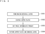
- FIG. 3 is a flowchart illustrating a procedure for manufacturing the bonded substrate according to Embodiment 1.
- FIGS. 4 to 6 are cross-sectional views schematically illustrating an intermediate product obtained during manufacturing of the bonded substrate according to Embodiment 1.
- Processes S101 to S104 in FIG. 3 are sequentially performed in manufacturing the bonded substrate according to Embodiment 1.
- brazing material layers 132 and 134 are formed on the principal surfaces 1101 and 1102 of the silicon nitride ceramic substrate 110, respectively, as illustrated in FIG. 4 .
- the brazing material layer 132 is also omitted.
- the brazing material layer 134 is also omitted.
- a paste containing an active metal braze and a solvent is prepared.
- the paste may further contain a binder, a dispersant, and an antifoaming agent.
- the prepared paste is screen-printed on the principal surfaces 1101 and 1102 of the silicon nitride ceramic substrate 110 to form first and second screen printed films on the principal surfaces 1101 and 1102 of the silicon nitride ceramic substrate 110, respectively.
- the solvent contained in the formed first and second screen printed films is vaporized. Consequently, the first and second screen printed films are changed into the brazing material layers 132 and 134, respectively.
- the brazing material layers 132 and 134 contain the active metal braze.
- the brazing material layers 132 and 134 may be formed in a method different from this.
- the active metal braze contains silver (Ag) powder, and at least one metal hydride powder selected from a group consisting of titanium hydride (TiH 2 ) powder and zirconium hydride (ZrH 2 ) powder.
- the active metal braze contains silver powder preferably higher than or equal to 40 wt% and lower than or equal to 80 wt%. Due to such a slight containment of the silver powder in the active metal braze, diffusion of silver constituting the silver powder into copper plates 111A and 113A and vanishment of the silver from bonding layers 112B and 114B in a process S103 to be described later are facilitated.
- the active metal braze consists of powder whose average particle diameter is preferably larger than or equal to 0.1 ⁇ m and smaller than or equal to 10 ⁇ m.
- the average particle diameter can be obtained by measuring the particle size distribution using a commercially available laser diffraction particle size distribution analyzer, and calculating D50 from the measured particle size distribution.
- the brazing material layers 132 and 134 can be thinner because the active metal braze consists of the powder with such a small average particle diameter.
- Each of the brazing material layers 132 and 134 has a thickness preferably greater than or equal to 0.1 ⁇ m and less than or equal to 5 ⁇ m. Due to such a slight thickness of the brazing material layers 132 and 134, the silver powder contained in the brazing material layers 132 and 134 are less, so that diffusion of silver constituting the silver powder into the copper plates 111A and 113A and vanishment of the silver from the bonding layers 112B and 114B in the process S103 to be described later are facilitated.
- the copper plates 111A and 113A are disposed on the formed brazing material layers 132 and 134, respectively, as illustrated in FIG. 5 . Accordingly, an intermediate product 100A including the silicon nitride ceramic substrate 110, the copper plate 111A, the brazing material layer 132, the copper plate 113A, and the brazing material layer 134 is obtained.
- the copper plate 111 and the bonding layer 112 are omitted from the bonded substrate 100
- disposing of the copper plate 111A is also omitted.
- the copper plate 113 and the bonding layer 114 are omitted from the bonded substrate 100, disposing of the copper plate 113A is also omitted.
- the obtained intermediate product 100A is thermally treated.
- the brazing material layers 132 and 134 are changed into the bonding layers 112B and 114B, respectively, as illustrated in FIG. 6 . Consequently, an intermediate product 100B including the silicon nitride ceramic substrate 110, the copper plate 111A, and the bonding layers 112B and 114B is obtained.
- the bonding layers 112B and 114B bond the copper plates 111A and 113A, respectively, to the silicon nitride ceramic substrate 110.
- the bonding layers 112B and 114B contain the compound of at least one element selected from the group consisting of titanium and zirconium and at least one element selected from the group consisting of nitrogen and silicon, and do not contain silver.
- the at least one element selected from the group consisting of nitrogen and silicon is supplied from the silicon nitride ceramic substrate 110.
- hot pressing is preferably performed to the intermediate product 100A.
- the intermediate product 100A is preferably pressed in a thickness direction of the silicon nitride ceramic substrate 110 in a vacuum or in an inert gas according to a surface pressure profile in which the highest surface pressure is greater than or equal to 5 MPa and less than or equal to 25 MPa, and is heated according to a temperature profile in which the highest temperature is greater than or equal to 800°C and less than or equal to 900°C.
- the brazing material layers 132 and 134 can bond the copper plates 111A and 113A, respectively, to the silicon nitride ceramic substrate 110 without forming voids. Furthermore, since the brazing material layers 132 and 134 can be thinned without forming voids, silver contained in the brazing material layers 132 and 134 can be less, and diffusion of the silver into the copper plates 111A and 113A and vanishment of the silver from the bonding layers 112B and 114B are facilitated.
- the copper plate 111A, the bonding layer 112B, the copper plate 113A, and the bonding layer 114B are patterned. Consequently, the copper plates 111A and 113A are changed into the patterned copper plates 111 and 113, respectively, as illustrated in FIG. 1 . Furthermore, the bonding layers 112B and 114B are changed into the patterned bonding layers 112 and 114, respectively, as illustrated in FIG. 1 .
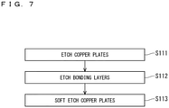
- FIG. 7 is a flowchart illustrating a procedure for patterning copper plates and bonding layers in manufacturing the bonded substrate according to Embodiment 1.
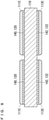
- FIGS. 8 and 9 are cross-sectional views each schematically illustrating an intermediate product obtained during pattering of the copper plates and the bonding layers in manufacturing the bonded substrate according to Embodiment 1.
- Processes Sill to S113 in FIG. 7 are sequentially performed as pattering the copper plate 111A, the bonding layer 112B, the copper plate 113A, and the bonding layer 114B in manufacturing the bonded substrate 100 according to Embodiment 1.
- the copper plates 111A and 113A are etched. Thereby, parts of the copper plates 111A and 113A are removed, so that the copper plates 111A and 113A are changed into etched copper plates 111C and 113C, respectively, as illustrated in FIG. 8 .
- a first portion 140 positioning between the silicon nitride ceramic substrate 110 and the etched copper plate 111C, and a second portion 141 positioning except between the silicon nitride ceramic substrate 110 and the etched copper plate 111C are formed in the bonding layer 112B.
- a first portion 142 positioning between the silicon nitride ceramic substrate 110 and the etched copper plate 113C, and a second portion 143 positioning except between the silicon nitride ceramic substrate 110 and the etched copper plate 113C are formed in the bonding layer 114B.
- Etching solutions such as aqueous iron chloride solutions and aqueous copper chloride solutions can be used for etching the copper plates 111C and 113C.
- the formed second portions 141 and 143 are etched as illustrated in FIG. 9 . Thereby, the second portions 141 and 143 are removed, and the first portions 140 and 142 remain. It is the remaining first portions 140 and 142 that are bonding layers 120 and 122, respectively.
- the second portions 141 and 143 can be etched using etching solutions such as ammonium fluoride solutions.
- the etched copper plates 111C and 113C are soft etched. This removes the vicinity of the end portions of the etched copper plates 111C and 113C. Furthermore, the etched copper plate 111C and 113C are changed into the patterned copper plates 111 and 113, respectively, as illustrated in FIG. 1 .
- the interplate portions 120 and 122 illustrated in FIG. 1 and the protruding portions 121 and 123 illustrated in FIG. 1 are formed in the etched bonding layers 140 and 142, respectively.
- Etching solutions such as aqueous iron chloride solutions and aqueous copper chloride solutions can be used for soft etching the copper plates 111C and 113C.
- the bonding layers 112B and 114B do not contain silver and copper that are susceptible to removal by the etching solutions. Thus, a decrease in the flatness due to removal of silver or copper hardly occurs in the processes Sill to S113.
- the bonded substrates 100 were manufactured according to the aforementioned method for manufacturing the bonded substrate 100.
- the bonded substrate 100 was manufactured, according to a method for manufacturing the bonded substrate 100 similar to the aforementioned method for manufacturing the bonded substrate 100 except for using an active metal braze containing larger amounts of silver and copper, using the brazing material layers 132 and 134 that is 15 ⁇ m thick, and pressing the intermediate product 100A in the thickness direction of the silicon nitride ceramic substrate 110 according to a surface pressure profile in which the highest surface pressure is 0.2 MPa.
- a width of the space between the adjacent protruding portions 121 was 1 mm.
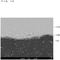
- Example 1 the cross section of the intermediate product 100B obtained during manufacturing of the bonded substrate 100 was observed with a scanning electron microscope (SEM).
- FIG. 10 illustrates an SEM image obtained through the observation. It can be understood from the SEM image that the bonding layer 112B has a uniform thickness and silver contained in the bonding layer 112B is less.
- FIG. 11 illustrates an SEM image obtained through the observation. It can be understood from the SEM image that a decrease in the flatness of the upper surface 121U of the protruding portion 121 due to removal of silver or copper hardly occurs.
- the surface roughness of the upper surface 121U of the protruding portion 121 and the principal surface 1101 of the silicon nitride ceramic substrate 110 of each of the manufactured bonded substrates 100 was evaluated.
- the surface profiles of the upper surface 121U and the principal surface 1101 were measured using a surface roughness measuring instrument SURFCOM 480A manufactured by TOKYO SEIMITSU CO., LTD to yield arithmetic average roughness Ra and the maximum height Rz of each of the upper surface 121U and the principal surface 1101. The result is shown in Table 1.
- the electrical insulating properties of the manufactured bonded substrates 100 were evaluated.
- a test of applying a voltage of 1 kV between the adjacent copper plates 111 for 1,000 hours in an environment at 85°C and 85% RH was conducted on the manufactured bonded substrates 100 to verify whether the electrical insulating properties after the test are inferior to those before the test. The result is shown in Table 1.
- the surface roughness of the upper surface 121U of the protruding portion 121 of each of the bonded substrates 100 in Examples 1 to 3 is significantly less than that in Comparative Example 1. Furthermore, the surface roughness of the upper surface 121U of the protruding portion 121 of the bonded substrates 100 is closer to the surface roughness of the principal surface 1101 of the silicon nitride ceramic substrate 110 of the bonded substrate 100 in each of Examples 1 to 3. This means that the flatness of the principal surface 1101 of the silicon nitride ceramic substrate 110 is reflected on the flatness of the upper surface 121U of the protruding portion 121 almost as it is because the protruding portion 121 has the uniform thickness.
Landscapes
- Engineering & Computer Science (AREA)
- Chemical & Material Sciences (AREA)
- Mechanical Engineering (AREA)
- Ceramic Engineering (AREA)
- Materials Engineering (AREA)
- Microelectronics & Electronic Packaging (AREA)
- Structural Engineering (AREA)
- Organic Chemistry (AREA)
- Manufacturing & Machinery (AREA)
- Ceramic Products (AREA)
- Manufacturing Of Printed Wiring (AREA)
Abstract
Description
- The present invention relates to a bonded substrate.
- Silicon nitride ceramics have high thermal conductivity and high insulating properties. Thus, a bonded substrate in which a copper plate is bonded to a silicon nitride ceramic substrate through a bonding layer is favorably used as an insulating heat-dissipating substrate on which a power semiconductor device is mounted.
- In many cases, such a bonded substrate is manufactured by preparing an intermediate product in which a brazing material layer is interposed between a copper plate and a silicon nitride ceramic substrate, changing the brazing material layer into a bonding layer through thermal treatment on the prepared intermediate product, and patterning the copper plate and the bonding layer.
- To prevent a defect of the bonded substrate which is caused by concentration of stress to end portions of the copper plate, forming, in the bonding layer, a protruding portion protruding from between the silicon nitride ceramic substrate and the copper plate is proposed.
- For example, in a ceramic circuit board described in Patent Document 1, a copper circuit plate is bonded through a brazing material layer to at least one surface of a ceramic substrate made of silicon nitride (paragraphs 0013 and 0020). The ceramic circuit board includes the brazing material layer interposed between the copper circuit plate and the ceramic substrate, and a brazing material protruding portion that protrudes outward at the side surface of the copper circuit plate (paragraph 0013). The brazing material layer is made of a brazing material containing Ag, Cu, and Ti (paragraph 0013). The brazing material protruding portion does not have a high flatness, and includes holes that expose the ceramic substrate (
FIG. 7 ). - [Patent Document 1]
Japanese Patent No. 6158144 - Conventional bonded substrates each including a protruding portion of a bonding layer as represented by the ceramic circuit board described in Patent Document 1 sometimes do not exhibit favorable electrical insulating properties between adjacent copper plates. For example, the electrical insulating properties between the adjacent copper plates sometimes deteriorate when a DC electric field or an AC electric field of several kV/mm is applied in an environment at 85°C and 85% RH.
- The present invention has been conceived in consideration of this problem. The problem to be solved by the present invention is to provide a bonded substrate that can improve electrical insulating properties between adjacent copper plates while preventing a defect of the bonded substrate which is caused by concentration of stress to end portions of the copper plates.
- A bonded substrate includes a silicon nitride ceramic substrate, a copper plate, and a bonding layer. The copper plate and the bonding layer are disposed on the silicon nitride ceramic substrate. The bonding layer bonds the copper plate to the silicon nitride ceramic substrate. The bonding layer includes: an interplate portion between the silicon nitride ceramic substrate and the copper plate; and a protruding portion protruding from between the silicon nitride ceramic substrate and the copper plate. The protruding portion covers the silicon nitride ceramic substrate to prevent exposure of the silicon nitride ceramic substrate.
- According to the present invention, the protruding portion relaxes the concentration of stress to end portions of the copper plate. This can prevent a defect of the bonded substrate which is caused by the concentration of the stress to the end portions of the copper plate.
- Furthermore, a chemical residue causing a decrease in the electrical insulating properties less likely remains on the protruding portion according to the present invention. This can improve the electrical insulating properties of the bonded substrate.
- The object, features, aspects, and advantages of the present invention will become more apparent from the following detailed description and the accompanying drawings.
-
-
FIG. 1 is a cross-sectional view schematically illustrating a bonded substrate according to Embodiment 1. -
FIG. 2 is an enlarged cross-sectional view schematically illustrating a portion of the bonded substrate according to Embodiment 1. -
FIG. 3 is a flowchart illustrating a procedure for manufacturing the bonded substrate according to Embodiment 1. -
FIG. 4 is a cross-sectional view schematically illustrating an intermediate product obtained during manufacturing of the bonded substrate according to Embodiment 1. -
FIG. 5 is a cross-sectional view schematically illustrating an intermediate product obtained during manufacturing of the bonded substrate according to Embodiment 1. -
FIG. 6 is a cross-sectional view schematically illustrating an intermediate product obtained during manufacturing of the bonded substrate according to Embodiment 1. -
FIG. 7 is a flowchart illustrating a procedure for patterning copper plates and bonding layers in manufacturing the bonded substrate according to Embodiment 1. -
FIG. 8 is a cross-sectional view schematically illustrating an intermediate product obtained during pattering of the copper plates and the bonding layers in manufacturing the bonded substrate according to Embodiment 1. -
FIG. 9 is a cross-sectional view schematically illustrating an intermediate product obtained during pattering of the copper plates and the bonding layers in manufacturing the bonded substrate according to Embodiment 1. -
FIG. 10 illustrates a scanning electron microscope (SEM) image of a cross section of an intermediate product obtained during manufacturing of a bonded substrate in Example 1. -
FIG. 11 illustrates an SEM image of a cross section of the bonded substrate manufactured in Example 1. - The protruding portion included in each of the conventional bonded substrates as represented by the ceramic circuit board described in Patent Document 1 contains silver and copper. Furthermore, silver and copper contained in the protruding portion are susceptible to removal during manufacturing of the bonded substrate, particularly, during etching while the bonded substrate is being manufactured. Thus, the protruding portion does not have a high flatness. When the protruding portion does not have a high flatness, a chemical residue causing a decrease in the electrical insulating properties likely remains on the protruding portion. This is a significant cause of the decrease in the electrical insulating properties in the conventional bonded substrates. A chemical solution causing the chemical residue is, for example, a chemical solution to be used for etching a copper plate and a bonding layer, or a chemical solution to be used for cleaning the surface of the copper plate through acid cleaning. The chemical residue is made of, for example, hydrochloric acid or sulfuric acid contained in the chemical solution. When the chemical residue remains on the protruding portion, silver or copper contained in the protruding portion or an alloy including the silver and the copper contained in the protruding portion sometimes causes ion migration. This problem obviously emerges, particularly, when a DC electric field or an AC electric field of several kV/mm is applied between adjacent protruding portions in a hot-humid environment, for example, at 85°C and 85% RH.
-
FIG. 1 is a cross-sectional view schematically illustrating a bonded substrate according to Embodiment 1.FIG. 2 is an enlarged cross-sectional view schematically illustrating a portion of the bonded substrate according to Embodiment 1.FIG. 2 is an enlarged view of a portion A ofFIG. 1 . - As illustrated in
FIGS. 1 and2 , abonded substrate 100 according to Embodiment 1 includes a silicon nitrideceramic substrate 110, acopper plate 111, abonding layer 112, acopper plate 113, and abonding layer 114. Thebonded substrate 100 may include elements other than these. One of a pair of thecopper plate 111 and thebonding layer 112 and a pair of thecopper plate 113 and thebonding layer 114 may be omitted. - The
copper plates ceramic substrate 110 through thebonding layers copper plates principal surfaces ceramic substrate 110 through thebonding layers - Applications of the
bonded substrate 100 may be any. Thebonded substrate 100 is used as, for example, an insulating heat-dissipating substrate on which a power semiconductor device is mounted. - As illustrated in
FIGS. 1 and2 , thecopper plate 111 and thebonding layer 112 are placed on theprincipal surface 1101 of the silicon nitrideceramic substrate 110. As illustrated inFIG. 1 , thecopper plate 113 and thebonding layer 114 are placed on theprincipal surface 1102 of the siliconnitride ceramic substrate 110. - The bonding layers 112 and 114 bond the
copper plates principal surfaces nitride ceramic substrate 110, respectively. - The
bonding layer 112 includes aninterplate portion 120 and a protrudingportion 121. Theinterplate portion 120 is interposed between the siliconnitride ceramic substrate 110 and thecopper plate 111. The protrudingportion 121 protrudes from between the siliconnitride ceramic substrate 110 and thecopper plate 111. Thebonding layer 114 includes aninterplate portion 122 and a protrudingportion 123. Theinterplate portion 122 is interposed between the siliconnitride ceramic substrate 110 and thecopper plate 113. The protrudingportion 123 protrudes from between the siliconnitride ceramic substrate 110 and thecopper plate 113. In the bondedsubstrate 100, the protrudingportions copper plates substrate 100 which is caused by the concentration of the stress to the end portions of thecopper plates - Each of the bonding layers 112 and 114 has a thickness preferably greater than or equal to 0.1 µm and less than or equal to 3 µm. The bonding layers 112 and 114 are so thin that the concentration of the stress to the end portions of the
copper plates - The protruding
portions principal surfaces nitride ceramic substrate 110 to prevent exposure of theprincipal surfaces portions nitride ceramic substrate 110, unlike the brazing material protruding portion included in the ceramic circuit board described inJapanese Patent No. 6158144 - Each of an
upper surface 121U of the protrudingportion 121 and anupper surface 123U of the protrudingportion 123 preferably has arithmetic average roughness Ra less than or equal to 0.7 µm, and the maximum height Rz less than or equal to 5 µm. - The protruding
portions portions substrate 100. - The bonding layers 112 and 114 contain a compound of at least one element selected from a group consisting of titanium (Ti) and zirconium (Zr) and at least one element selected from a group consisting of nitrogen (N) and silicon (Si), and do not contain silver (Ag) and copper (Cu) generally included in bonding layers. Thus, the protruding
portions substrate 100, particularly, during etching while the bondedsubstrate 100 is being manufactured. Consequently, a decrease in the flatness of the bonding layers 112 and 114 during manufacturing of the bondedsubstrate 100 can be prevented. -
FIG. 3 is a flowchart illustrating a procedure for manufacturing the bonded substrate according to Embodiment 1.FIGS. 4 to 6 are cross-sectional views schematically illustrating an intermediate product obtained during manufacturing of the bonded substrate according to Embodiment 1. - Processes S101 to S104 in
FIG. 3 are sequentially performed in manufacturing the bonded substrate according to Embodiment 1. - In the process S101, brazing
material layers principal surfaces nitride ceramic substrate 110, respectively, as illustrated inFIG. 4 . In the case that thecopper plate 111 and thebonding layer 112 are omitted from the bondedsubstrate 100, forming of thebrazing material layer 132 is also omitted. In the case that thecopper plate 113 and thebonding layer 114 are omitted from the bondedsubstrate 100, forming of thebrazing material layer 134 is also omitted. - At the formation of the brazing material layers 132 and 134, a paste containing an active metal braze and a solvent is prepared. The paste may further contain a binder, a dispersant, and an antifoaming agent. Next, the prepared paste is screen-printed on the
principal surfaces nitride ceramic substrate 110 to form first and second screen printed films on theprincipal surfaces nitride ceramic substrate 110, respectively. Then, the solvent contained in the formed first and second screen printed films is vaporized. Consequently, the first and second screen printed films are changed into the brazing material layers 132 and 134, respectively. The brazing material layers 132 and 134 contain the active metal braze. The brazing material layers 132 and 134 may be formed in a method different from this. - The active metal braze contains silver (Ag) powder, and at least one metal hydride powder selected from a group consisting of titanium hydride (TiH2) powder and zirconium hydride (ZrH2) powder.
- The active metal braze contains silver powder preferably higher than or equal to 40 wt% and lower than or equal to 80 wt%. Due to such a slight containment of the silver powder in the active metal braze, diffusion of silver constituting the silver powder into
copper plates layers - The active metal braze consists of powder whose average particle diameter is preferably larger than or equal to 0.1 µm and smaller than or equal to 10 µm. The average particle diameter can be obtained by measuring the particle size distribution using a commercially available laser diffraction particle size distribution analyzer, and calculating D50 from the measured particle size distribution. The brazing material layers 132 and 134 can be thinner because the active metal braze consists of the powder with such a small average particle diameter.
- Each of the brazing material layers 132 and 134 has a thickness preferably greater than or equal to 0.1 µm and less than or equal to 5 µm. Due to such a slight thickness of the brazing material layers 132 and 134, the silver powder contained in the brazing material layers 132 and 134 are less, so that diffusion of silver constituting the silver powder into the
copper plates - In the process S102, the
copper plates FIG. 5 . Accordingly, anintermediate product 100A including the siliconnitride ceramic substrate 110, thecopper plate 111A, thebrazing material layer 132, thecopper plate 113A, and thebrazing material layer 134 is obtained. When thecopper plate 111 and thebonding layer 112 are omitted from the bondedsubstrate 100, disposing of thecopper plate 111A is also omitted. When thecopper plate 113 and thebonding layer 114 are omitted from the bondedsubstrate 100, disposing of thecopper plate 113A is also omitted. - In the process S103, the obtained
intermediate product 100A is thermally treated. Through this treatment, the brazing material layers 132 and 134 are changed into the bonding layers 112B and 114B, respectively, as illustrated inFIG. 6 . Consequently, anintermediate product 100B including the siliconnitride ceramic substrate 110, thecopper plate 111A, and the bonding layers 112B and 114B is obtained. The bonding layers 112B and 114B bond thecopper plates nitride ceramic substrate 110. While the brazing material layers 132 and 134 are changed into the bonding layers 112B and 114B, respectively, silver constituting the silver powder contained in the brazing material layers 132 and 134 are diffused into thecopper plates nitride ceramic substrate 110. - In the process S103, hot pressing is preferably performed to the
intermediate product 100A. In the hot pressing, theintermediate product 100A is preferably pressed in a thickness direction of the siliconnitride ceramic substrate 110 in a vacuum or in an inert gas according to a surface pressure profile in which the highest surface pressure is greater than or equal to 5 MPa and less than or equal to 25 MPa, and is heated according to a temperature profile in which the highest temperature is greater than or equal to 800°C and less than or equal to 900°C. With this condition, even when the brazing material layers 132 and 134 are thin such as in the case where each of the brazing material layers 132 and 134 has a thickness greater than or equal to 0.1 µm and less than or equal to 5 µm, the brazing material layers 132 and 134 can bond thecopper plates nitride ceramic substrate 110 without forming voids. Furthermore, since the brazing material layers 132 and 134 can be thinned without forming voids, silver contained in the brazing material layers 132 and 134 can be less, and diffusion of the silver into thecopper plates copper plates - In the process S104, the
copper plate 111A, thebonding layer 112B, thecopper plate 113A, and thebonding layer 114B are patterned. Consequently, thecopper plates copper plates FIG. 1 . Furthermore, the bonding layers 112B and 114B are changed into the patternedbonding layers FIG. 1 . -
FIG. 7 is a flowchart illustrating a procedure for patterning copper plates and bonding layers in manufacturing the bonded substrate according to Embodiment 1.FIGS. 8 and9 are cross-sectional views each schematically illustrating an intermediate product obtained during pattering of the copper plates and the bonding layers in manufacturing the bonded substrate according to Embodiment 1. - Processes Sill to S113 in
FIG. 7 are sequentially performed as pattering thecopper plate 111A, thebonding layer 112B, thecopper plate 113A, and thebonding layer 114B in manufacturing the bondedsubstrate 100 according to Embodiment 1. - In the process Sill, the
copper plates copper plates copper plates copper plates FIG. 8 . Concurrently, afirst portion 140 positioning between the siliconnitride ceramic substrate 110 and the etchedcopper plate 111C, and asecond portion 141 positioning except between the siliconnitride ceramic substrate 110 and the etchedcopper plate 111C are formed in thebonding layer 112B. Afirst portion 142 positioning between the siliconnitride ceramic substrate 110 and the etchedcopper plate 113C, and asecond portion 143 positioning except between the siliconnitride ceramic substrate 110 and the etchedcopper plate 113C are formed in thebonding layer 114B. Etching solutions such as aqueous iron chloride solutions and aqueous copper chloride solutions can be used for etching thecopper plates - In the process S112, the formed
second portions FIG. 9 . Thereby, thesecond portions first portions first portions layers second portions - In the process S113, the etched
copper plates copper plates copper plate copper plates FIG. 1 . Theinterplate portions FIG. 1 and the protrudingportions FIG. 1 are formed in the etchedbonding layers copper plates - As described above, the bonding layers 112B and 114B do not contain silver and copper that are susceptible to removal by the etching solutions. Thus, a decrease in the flatness due to removal of silver or copper hardly occurs in the processes Sill to S113.
- In Examples 1 to 3, the bonded
substrates 100 were manufactured according to the aforementioned method for manufacturing the bondedsubstrate 100. In Comparative Example 1, the bondedsubstrate 100 was manufactured, according to a method for manufacturing the bondedsubstrate 100 similar to the aforementioned method for manufacturing the bondedsubstrate 100 except for using an active metal braze containing larger amounts of silver and copper, using the brazing material layers 132 and 134 that is 15 µm thick, and pressing theintermediate product 100A in the thickness direction of the siliconnitride ceramic substrate 110 according to a surface pressure profile in which the highest surface pressure is 0.2 MPa. In Examples 1 to 3 and Comparative Example 1, a width of the space between the adjacent protrudingportions 121 was 1 mm. - In Example 1, the cross section of the
intermediate product 100B obtained during manufacturing of the bondedsubstrate 100 was observed with a scanning electron microscope (SEM).FIG. 10 illustrates an SEM image obtained through the observation. It can be understood from the SEM image that thebonding layer 112B has a uniform thickness and silver contained in thebonding layer 112B is less. - Furthermore, the cross section of the bonded
substrate 100 manufactured in Example 1 was observed with the SEM.FIG. 11 illustrates an SEM image obtained through the observation. It can be understood from the SEM image that a decrease in the flatness of theupper surface 121U of the protrudingportion 121 due to removal of silver or copper hardly occurs. - The surface roughness of the
upper surface 121U of the protrudingportion 121 and theprincipal surface 1101 of the siliconnitride ceramic substrate 110 of each of the manufactured bondedsubstrates 100 was evaluated. For evaluating the surface roughness, the surface profiles of theupper surface 121U and theprincipal surface 1101 were measured using a surface roughness measuring instrument SURFCOM 480A manufactured by TOKYO SEIMITSU CO., LTD to yield arithmetic average roughness Ra and the maximum height Rz of each of theupper surface 121U and theprincipal surface 1101. The result is shown in Table 1. - Furthermore, the electrical insulating properties of the manufactured bonded
substrates 100 were evaluated. For evaluating the electrical insulating properties, a test of applying a voltage of 1 kV between theadjacent copper plates 111 for 1,000 hours in an environment at 85°C and 85% RH was conducted on the manufactured bondedsubstrates 100 to verify whether the electrical insulating properties after the test are inferior to those before the test. The result is shown in Table 1.[Table 1] Principal surface of silicon nitride ceramic substrate Principal surface of protruding portion Evaluation of insulation resistance Ra (µm) Rz (µm) Ra (µm) Rz (µm) No deterioration Example 1 0.32 1.84 0.34 2.15 No deterioration Example 2 0.32 1.84 0.38 2.26 No deterioration Example 3 0.32 1.84 0.33 2.09 No deterioration Comparative Example 1 0.32 1.84 3.2 15.1 Deterioration - As seen from Table 1, the surface roughness of the
upper surface 121U of the protrudingportion 121 of each of the bondedsubstrates 100 in Examples 1 to 3 is significantly less than that in Comparative Example 1. Furthermore, the surface roughness of theupper surface 121U of the protrudingportion 121 of the bondedsubstrates 100 is closer to the surface roughness of theprincipal surface 1101 of the siliconnitride ceramic substrate 110 of the bondedsubstrate 100 in each of Examples 1 to 3. This means that the flatness of theprincipal surface 1101 of the siliconnitride ceramic substrate 110 is reflected on the flatness of theupper surface 121U of the protrudingportion 121 almost as it is because the protrudingportion 121 has the uniform thickness. While the electrical insulating properties after the test are inferior to those before the test in the bondedsubstrate 100 of Comparative Example 1, the electrical insulating properties after the test are not inferior to those before the test in the bondedsubstrates 100 of Examples 1 to 3. It can be understood that the electrical insulating properties between theadjacent copper plates 111 in the bondedsubstrates 100 of Examples 1 to 3 are improved. - While the present invention is described in detail above, the foregoing description is in all aspects illustrative and does not restrict the invention. It is understood that numerous modifications that have not yet been described can be devised without departing from the scope of the invention.
-
- 100 bonded substrate
- 110 silicon nitride ceramic substrate
- 111, 113, 111A, 113A copper plate
- 112, 114, 112B, 114B bonding layer
- 120, 122 interplate portion
- 121, 123 protruding portion
- 132, 134 brazing material layer
- 100A intermediate product
- 140 first portion
- 141 second portion
Claims (3)
- A bonded substrate, comprising:a silicon nitride ceramic substrate;a copper plate disposed on the silicon nitride ceramic substrate; anda bonding layer disposed on the silicon nitride ceramic substrate, bonding the copper plate to the silicon nitride ceramic substrate, and including: an interplate portion between the silicon nitride ceramic substrate and the copper plate; and a protruding portion protruding from between the silicon nitride ceramic substrate and the copper plate, the protruding portion covering the silicon nitride ceramic substrate to prevent exposure of the silicon nitride ceramic substrate.
- The bonded substrate according to claim 1,
wherein an upper surface of the bonding layer has arithmetic average roughness Ra less than or equal to 0.7 µm, and a maximum height Rz less than or equal to 5 µm. - The bonded substrate according to claim 1 or 2,
wherein the protruding portion does not contain silver and copper.
Applications Claiming Priority (1)
| Application Number | Priority Date | Filing Date | Title |
|---|---|---|---|
| PCT/JP2019/010545 WO2020183701A1 (en) | 2019-03-14 | 2019-03-14 | Bonded substrate |
Publications (2)
| Publication Number | Publication Date |
|---|---|
| EP3941166A1 true EP3941166A1 (en) | 2022-01-19 |
| EP3941166A4 EP3941166A4 (en) | 2022-11-09 |
Family
ID=72426068
Family Applications (1)
| Application Number | Title | Priority Date | Filing Date |
|---|---|---|---|
| EP19919323.6A Pending EP3941166A4 (en) | 2019-03-14 | 2019-03-14 | Bonded substrate |
Country Status (4)
| Country | Link |
|---|---|
| US (1) | US12679778B2 (en) |
| EP (1) | EP3941166A4 (en) |
| JP (1) | JP7197677B2 (en) |
| WO (1) | WO2020183701A1 (en) |
Families Citing this family (4)
| Publication number | Priority date | Publication date | Assignee | Title |
|---|---|---|---|---|
| CN112679220A (en) * | 2020-12-30 | 2021-04-20 | 中国电子科技集团公司第十三研究所 | Silicon nitride ceramic copper-clad substrate and preparation method thereof |
| JP7708622B2 (en) * | 2021-09-10 | 2025-07-15 | デンカ株式会社 | Ceramic Composite Substrate |
| JP7620726B2 (en) * | 2021-10-25 | 2025-01-23 | 株式会社東芝 | Ceramic copper circuit board and semiconductor device using same |
| EP4311818A1 (en) * | 2022-07-29 | 2024-01-31 | Heraeus Electronics GmbH & Co. KG | Metal-ceramic substrate with contact area |
Family Cites Families (14)
| Publication number | Priority date | Publication date | Assignee | Title |
|---|---|---|---|---|
| JPS55162944A (en) | 1979-06-08 | 1980-12-18 | Sanyo Electric Co Ltd | Multi-cylinder popsicle dispenser |
| JPH10190176A (en) | 1996-12-26 | 1998-07-21 | Denki Kagaku Kogyo Kk | Circuit board |
| JP5038565B2 (en) * | 2000-09-22 | 2012-10-03 | 株式会社東芝 | Ceramic circuit board and manufacturing method thereof |
| JP4345066B2 (en) * | 2005-05-24 | 2009-10-14 | 日立金属株式会社 | Ceramic circuit board and power semiconductor module using the same |
| PL2480052T3 (en) | 2009-09-15 | 2018-01-31 | Toshiba Kk | Ceramic printed circuit board and the method of its production |
| JP5976678B2 (en) * | 2011-12-20 | 2016-08-24 | 株式会社東芝 | Ceramic copper circuit board |
| JP6400422B2 (en) | 2014-10-07 | 2018-10-03 | Dowaメタルテック株式会社 | Metal-ceramic circuit board and manufacturing method thereof |
| EP3321957B1 (en) * | 2015-07-09 | 2022-07-27 | Kabushiki Kaisha Toshiba | Ceramic metal circuit board and semiconductor device using same |
| JP6499545B2 (en) | 2015-08-07 | 2019-04-10 | Jx金属株式会社 | Metal-ceramic bonding substrate and manufacturing method thereof |
| EP3629370B1 (en) * | 2015-09-28 | 2022-08-31 | Kabushiki Kaisha Toshiba | Circuit substrate and semiconductor device |
| WO2017115461A1 (en) | 2015-12-28 | 2017-07-06 | Ngk Insulators, Ltd. | Bonded substrate and method for manufacturing bonded substrate |
| CN109155291B (en) | 2016-05-19 | 2022-05-03 | 三菱综合材料株式会社 | Substrate for power module |
| JP6654613B2 (en) | 2016-12-22 | 2020-02-26 | 三ツ星ベルト株式会社 | Conductive paste, electronic substrate and method of manufacturing the same |
| KR20210107699A (en) * | 2018-12-28 | 2021-09-01 | 덴카 주식회사 | Method for manufacturing ceramic-copper composite, ceramic circuit board, power module and ceramic-copper composite |
-
2019
- 2019-03-14 JP JP2021505452A patent/JP7197677B2/en active Active
- 2019-03-14 EP EP19919323.6A patent/EP3941166A4/en active Pending
- 2019-03-14 WO PCT/JP2019/010545 patent/WO2020183701A1/en not_active Ceased
-
2021
- 2021-08-30 US US17/460,694 patent/US12679778B2/en active Active
Also Published As
| Publication number | Publication date |
|---|---|
| US12679778B2 (en) | 2026-07-14 |
| JP7197677B2 (en) | 2022-12-27 |
| US20210387923A1 (en) | 2021-12-16 |
| EP3941166A4 (en) | 2022-11-09 |
| WO2020183701A1 (en) | 2020-09-17 |
| JPWO2020183701A1 (en) | 2021-12-16 |
Similar Documents
| Publication | Publication Date | Title |
|---|---|---|
| US20210387923A1 (en) | Bonded substrate | |
| EP2727898B1 (en) | Brazing filler metal, brazing filler metal paste, ceramic circuit substrate, and ceramic master circuit substrate | |
| JP7332588B2 (en) | Ceramic copper circuit board and manufacturing method thereof | |
| JP6271628B2 (en) | Power module | |
| US6768079B2 (en) | Susceptor with built-in plasma generation electrode and manufacturing method therefor | |
| EP3632879A1 (en) | Ceramic circuit board and module using same | |
| US11917752B2 (en) | Bonded substrate and manufacturing method of bonded substrate | |
| EP3661337A1 (en) | Ceramic circuit board and production method therefor | |
| EP2811513A1 (en) | Substrate for power modules, substrate with heat sink for power modules, power module, method for producing substrate for power modules, and paste for bonding copper member | |
| EP3632880B1 (en) | Ceramic circuit board and method for producing same | |
| US12109640B2 (en) | Ceramic-copper composite, ceramic circuit board, power module, and method of producing ceramic-copper composite | |
| EP4071126A1 (en) | Bonded substrate and method for manufacturing bonded substrate | |
| EP4310066A1 (en) | Composite substrate | |
| JP2026074215A (en) | Metal-ceramic bonded substrate | |
| EP4407672A1 (en) | Metal-ceramic bonding substrate, and method for manufacturing same | |
| JP2004172182A (en) | Circuit board and method of manufacturing the same | |
| JP7289910B2 (en) | BONDED SUBSTRATE AND BONDED SUBSTRATE MANUFACTURING METHOD | |
| WO2020196616A1 (en) | Circuit board, electronic device, and electronic module | |
| WO2023234286A1 (en) | Ceramic circuit substrate and semiconductor device using same | |
| WO2022210477A1 (en) | Joint structure | |
| JP7680252B2 (en) | Method for manufacturing a circuit board and a semiconductor module | |
| EP4482262A1 (en) | Ceramic composite substrate, and method for manufacturing ceramic composite substrate | |
| EP4482261A1 (en) | Ceramic composite substrate, and production method for ceramic composite substrate | |
| EP4310065A1 (en) | Composite substrate | |
| JPH09283657A (en) | Circuit board and method of manufacturing the same |
Legal Events
| Date | Code | Title | Description |
|---|---|---|---|
| STAA | Information on the status of an ep patent application or granted ep patent |
Free format text: STATUS: THE INTERNATIONAL PUBLICATION HAS BEEN MADE |
|
| PUAI | Public reference made under article 153(3) epc to a published international application that has entered the european phase |
Free format text: ORIGINAL CODE: 0009012 |
|
| STAA | Information on the status of an ep patent application or granted ep patent |
Free format text: STATUS: REQUEST FOR EXAMINATION WAS MADE |
|
| 17P | Request for examination filed |
Effective date: 20210910 |
|
| AK | Designated contracting states |
Kind code of ref document: A1 Designated state(s): AL AT BE BG CH CY CZ DE DK EE ES FI FR GB GR HR HU IE IS IT LI LT LU LV MC MK MT NL NO PL PT RO RS SE SI SK SM TR |
|
| DAV | Request for validation of the european patent (deleted) | ||
| DAX | Request for extension of the european patent (deleted) | ||
| A4 | Supplementary search report drawn up and despatched |
Effective date: 20221012 |
|
| RIC1 | Information provided on ipc code assigned before grant |
Ipc: B23K 103/12 20060101ALN20221006BHEP Ipc: C22C 5/08 20060101ALN20221006BHEP Ipc: B23K 103/00 20060101ALN20221006BHEP Ipc: B23K 103/16 20060101ALN20221006BHEP Ipc: H05K 3/12 20060101ALN20221006BHEP Ipc: H05K 3/10 20060101ALN20221006BHEP Ipc: H05K 3/06 20060101ALN20221006BHEP Ipc: B23K 1/19 20060101ALI20221006BHEP Ipc: C04B 37/02 20060101ALI20221006BHEP Ipc: B23K 35/02 20060101ALI20221006BHEP Ipc: B23K 35/00 20060101ALI20221006BHEP Ipc: B23K 1/00 20060101ALI20221006BHEP Ipc: H05K 1/02 20060101ALI20221006BHEP Ipc: H05K 1/03 20060101ALI20221006BHEP Ipc: H01L 23/13 20060101ALI20221006BHEP Ipc: H05K 3/38 20060101AFI20221006BHEP |
|
| STAA | Information on the status of an ep patent application or granted ep patent |
Free format text: STATUS: EXAMINATION IS IN PROGRESS |
|
| 17Q | First examination report despatched |
Effective date: 20251208 |