EP3940805A1 - Light-emitting device and electronic apparatus comprising same - Google Patents
Light-emitting device and electronic apparatus comprising same Download PDFInfo
- Publication number
- EP3940805A1 EP3940805A1 EP21184613.4A EP21184613A EP3940805A1 EP 3940805 A1 EP3940805 A1 EP 3940805A1 EP 21184613 A EP21184613 A EP 21184613A EP 3940805 A1 EP3940805 A1 EP 3940805A1
- Authority
- EP
- European Patent Office
- Prior art keywords
- group
- substituted
- compound
- formula
- unsubstituted
- Prior art date
- Legal status (The legal status is an assumption and is not a legal conclusion. Google has not performed a legal analysis and makes no representation as to the accuracy of the status listed.)
- Granted
Links
- 150000001875 compounds Chemical class 0.000 claims abstract description 362
- 239000010410 layer Substances 0.000 claims description 261
- 125000000623 heterocyclic group Chemical group 0.000 claims description 95
- 125000002837 carbocyclic group Chemical group 0.000 claims description 92
- 229910052757 nitrogen Inorganic materials 0.000 claims description 50
- 239000011229 interlayer Substances 0.000 claims description 47
- YZCKVEUIGOORGS-OUBTZVSYSA-N Deuterium Chemical compound [2H] YZCKVEUIGOORGS-OUBTZVSYSA-N 0.000 claims description 45
- 229910052805 deuterium Inorganic materials 0.000 claims description 45
- 125000001997 phenyl group Chemical group [H]C1=C([H])C([H])=C(*)C([H])=C1[H] 0.000 claims description 45
- 125000004093 cyano group Chemical group *C#N 0.000 claims description 41
- 238000006243 chemical reaction Methods 0.000 claims description 39
- 229910052760 oxygen Inorganic materials 0.000 claims description 39
- 229910052717 sulfur Inorganic materials 0.000 claims description 37
- 125000000714 pyrimidinyl group Chemical group 0.000 claims description 36
- 229910052799 carbon Inorganic materials 0.000 claims description 35
- 125000004122 cyclic group Chemical group 0.000 claims description 32
- 125000000449 nitro group Chemical group [O-][N+](*)=O 0.000 claims description 32
- 125000002887 hydroxy group Chemical group [H]O* 0.000 claims description 31
- 125000003373 pyrazinyl group Chemical group 0.000 claims description 30
- 125000006743 (C1-C60) alkyl group Chemical group 0.000 claims description 29
- 125000006746 (C1-C60) alkoxy group Chemical group 0.000 claims description 28
- 229910052739 hydrogen Inorganic materials 0.000 claims description 28
- 239000001257 hydrogen Substances 0.000 claims description 28
- 125000004429 atom Chemical group 0.000 claims description 27
- 125000006744 (C2-C60) alkenyl group Chemical group 0.000 claims description 25
- 125000006745 (C2-C60) alkynyl group Chemical group 0.000 claims description 25
- JUJWROOIHBZHMG-UHFFFAOYSA-N Pyridine Chemical group C1=CC=NC=C1 JUJWROOIHBZHMG-UHFFFAOYSA-N 0.000 claims description 23
- 125000006751 (C6-C60) aryloxy group Chemical group 0.000 claims description 21
- 125000006752 (C6-C60) arylthio group Chemical group 0.000 claims description 21
- 125000003118 aryl group Chemical group 0.000 claims description 21
- 150000002431 hydrogen Chemical class 0.000 claims description 20
- 125000004076 pyridyl group Chemical group 0.000 claims description 19
- BASFCYQUMIYNBI-UHFFFAOYSA-N platinum Chemical group [Pt] BASFCYQUMIYNBI-UHFFFAOYSA-N 0.000 claims description 18
- 125000004306 triazinyl group Chemical group 0.000 claims description 18
- KDLHZDBZIXYQEI-UHFFFAOYSA-N Palladium Chemical compound [Pd] KDLHZDBZIXYQEI-UHFFFAOYSA-N 0.000 claims description 17
- 125000006267 biphenyl group Chemical group 0.000 claims description 17
- 125000002098 pyridazinyl group Chemical group 0.000 claims description 16
- 125000002883 imidazolyl group Chemical group 0.000 claims description 15
- 125000005647 linker group Chemical group 0.000 claims description 15
- 125000002971 oxazolyl group Chemical group 0.000 claims description 15
- 125000003226 pyrazolyl group Chemical group 0.000 claims description 15
- 125000001425 triazolyl group Chemical group 0.000 claims description 15
- JYEUMXHLPRZUAT-UHFFFAOYSA-N 1,2,3-triazine Chemical group C1=CN=NN=C1 JYEUMXHLPRZUAT-UHFFFAOYSA-N 0.000 claims description 14
- PBMFSQRYOILNGV-UHFFFAOYSA-N pyridazine Chemical group C1=CC=NN=C1 PBMFSQRYOILNGV-UHFFFAOYSA-N 0.000 claims description 14
- 239000010409 thin film Substances 0.000 claims description 14
- PXHVJJICTQNCMI-UHFFFAOYSA-N Nickel Chemical compound [Ni] PXHVJJICTQNCMI-UHFFFAOYSA-N 0.000 claims description 13
- 125000001162 cycloheptenyl group Chemical group C1(=CCCCCC1)* 0.000 claims description 13
- 125000000582 cycloheptyl group Chemical group [H]C1([H])C([H])([H])C([H])([H])C([H])([H])C([H])(*)C([H])([H])C1([H])[H] 0.000 claims description 13
- 125000000596 cyclohexenyl group Chemical group C1(=CCCCC1)* 0.000 claims description 13
- 125000000113 cyclohexyl group Chemical group [H]C1([H])C([H])([H])C([H])([H])C([H])(*)C([H])([H])C1([H])[H] 0.000 claims description 13
- 125000000640 cyclooctyl group Chemical group [H]C1([H])C([H])([H])C([H])([H])C([H])([H])C([H])(*)C([H])([H])C([H])([H])C1([H])[H] 0.000 claims description 13
- 125000002433 cyclopentenyl group Chemical group C1(=CCCC1)* 0.000 claims description 13
- 125000001511 cyclopentyl group Chemical group [H]C1([H])C([H])([H])C([H])([H])C([H])(*)C1([H])[H] 0.000 claims description 13
- 125000000168 pyrrolyl group Chemical group 0.000 claims description 13
- IJGRMHOSHXDMSA-UHFFFAOYSA-N Atomic nitrogen Chemical compound N#N IJGRMHOSHXDMSA-UHFFFAOYSA-N 0.000 claims description 12
- 239000010931 gold Substances 0.000 claims description 12
- 125000003518 norbornenyl group Chemical group C12(C=CC(CC1)C2)* 0.000 claims description 12
- UGUHFDPGDQDVGX-UHFFFAOYSA-N 1,2,3-thiadiazole Chemical group C1=CSN=N1 UGUHFDPGDQDVGX-UHFFFAOYSA-N 0.000 claims description 10
- FZWLAAWBMGSTSO-UHFFFAOYSA-N Thiazole Chemical group C1=CSC=N1 FZWLAAWBMGSTSO-UHFFFAOYSA-N 0.000 claims description 10
- 229910052796 boron Inorganic materials 0.000 claims description 10
- ZLTPDFXIESTBQG-UHFFFAOYSA-N isothiazole Chemical group C=1C=NSC=1 ZLTPDFXIESTBQG-UHFFFAOYSA-N 0.000 claims description 10
- WCPAKWJPBJAGKN-UHFFFAOYSA-N oxadiazole Chemical group C1=CON=N1 WCPAKWJPBJAGKN-UHFFFAOYSA-N 0.000 claims description 10
- YLQBMQCUIZJEEH-UHFFFAOYSA-N Furan Chemical group C=1C=COC=1 YLQBMQCUIZJEEH-UHFFFAOYSA-N 0.000 claims description 9
- 239000010949 copper Substances 0.000 claims description 9
- 230000002950 deficient Effects 0.000 claims description 9
- QJGQUHMNIGDVPM-UHFFFAOYSA-N nitrogen group Chemical group [N] QJGQUHMNIGDVPM-UHFFFAOYSA-N 0.000 claims description 9
- UFHFLCQGNIYNRP-UHFFFAOYSA-N Hydrogen Chemical compound [H][H] UFHFLCQGNIYNRP-UHFFFAOYSA-N 0.000 claims description 8
- YTPLMLYBLZKORZ-UHFFFAOYSA-N Thiophene Chemical group C=1C=CSC=1 YTPLMLYBLZKORZ-UHFFFAOYSA-N 0.000 claims description 8
- ORILYTVJVMAKLC-UHFFFAOYSA-N adamantane Chemical group C1C(C2)CC3CC1CC2C3 ORILYTVJVMAKLC-UHFFFAOYSA-N 0.000 claims description 8
- MKCBRYIXFFGIKN-UHFFFAOYSA-N bicyclo[1.1.1]pentane Chemical group C1C2CC1C2 MKCBRYIXFFGIKN-UHFFFAOYSA-N 0.000 claims description 7
- JSMRMEYFZHIPJV-UHFFFAOYSA-N bicyclo[2.1.1]hexane Chemical group C1C2CC1CC2 JSMRMEYFZHIPJV-UHFFFAOYSA-N 0.000 claims description 7
- GPRLTFBKWDERLU-UHFFFAOYSA-N bicyclo[2.2.2]octane Chemical group C1CC2CCC1CC2 GPRLTFBKWDERLU-UHFFFAOYSA-N 0.000 claims description 7
- 229910052709 silver Inorganic materials 0.000 claims description 7
- 239000004332 silver Substances 0.000 claims description 7
- BQCADISMDOOEFD-UHFFFAOYSA-N Silver Chemical compound [Ag] BQCADISMDOOEFD-UHFFFAOYSA-N 0.000 claims description 6
- 125000000522 cyclooctenyl group Chemical group C1(=CCCCCCC1)* 0.000 claims description 6
- 230000003111 delayed effect Effects 0.000 claims description 6
- 229910052737 gold Inorganic materials 0.000 claims description 6
- CTAPFRYPJLPFDF-UHFFFAOYSA-N isoxazole Chemical group C=1C=NOC=1 CTAPFRYPJLPFDF-UHFFFAOYSA-N 0.000 claims description 6
- 229910052763 palladium Inorganic materials 0.000 claims description 6
- 229910052697 platinum Inorganic materials 0.000 claims description 6
- 150000003967 siloles Chemical group 0.000 claims description 6
- ZOXJGFHDIHLPTG-UHFFFAOYSA-N Boron Chemical compound [B] ZOXJGFHDIHLPTG-UHFFFAOYSA-N 0.000 claims description 5
- 229910052802 copper Inorganic materials 0.000 claims description 5
- PCHJSUWPFVWCPO-UHFFFAOYSA-N gold Chemical compound [Au] PCHJSUWPFVWCPO-UHFFFAOYSA-N 0.000 claims description 5
- 229910052759 nickel Inorganic materials 0.000 claims description 5
- 229910052710 silicon Inorganic materials 0.000 claims description 5
- OGZZEGWWYQKMSO-UHFFFAOYSA-N 1,2-dihydroazaborinine Chemical group B1NC=CC=C1 OGZZEGWWYQKMSO-UHFFFAOYSA-N 0.000 claims description 4
- HWIATMHDQVGMFQ-UHFFFAOYSA-N 1,3-azaborinine Chemical group B1=CC=CN=C1 HWIATMHDQVGMFQ-UHFFFAOYSA-N 0.000 claims description 4
- OBUDOIAYABJUHQ-UHFFFAOYSA-N 1,4-azaborinine Chemical group B1=CC=NC=C1 OBUDOIAYABJUHQ-UHFFFAOYSA-N 0.000 claims description 4
- HPKDMONSMXBYFI-UHFFFAOYSA-N 1,4-dihydroborinine Chemical group B1C=CCC=C1 HPKDMONSMXBYFI-UHFFFAOYSA-N 0.000 claims description 4
- KZCKBCXOMCLEQA-UHFFFAOYSA-N 2H-1,4-oxaborinine Chemical group C1OC=CB=C1 KZCKBCXOMCLEQA-UHFFFAOYSA-N 0.000 claims description 4
- FMJVJBYTTXEFBB-UHFFFAOYSA-N 2H-1,4-thiaborinine Chemical group S1CC=BC=C1 FMJVJBYTTXEFBB-UHFFFAOYSA-N 0.000 claims description 4
- RYGMFSIKBFXOCR-UHFFFAOYSA-N Copper Chemical compound [Cu] RYGMFSIKBFXOCR-UHFFFAOYSA-N 0.000 claims description 4
- KCQLSIKUOYWBAO-UHFFFAOYSA-N azaborinine Chemical group B1=NC=CC=C1 KCQLSIKUOYWBAO-UHFFFAOYSA-N 0.000 claims description 4
- 229910052698 phosphorus Inorganic materials 0.000 claims description 3
- 230000010287 polarization Effects 0.000 claims description 3
- -1 dimethylfluorenyl group Chemical group 0.000 description 183
- 230000015572 biosynthetic process Effects 0.000 description 100
- 238000003786 synthesis reaction Methods 0.000 description 98
- 0 **1cc2ncccc2[n]1I Chemical compound **1cc2ncccc2[n]1I 0.000 description 70
- 239000002019 doping agent Substances 0.000 description 68
- 239000000463 material Substances 0.000 description 38
- 239000010408 film Substances 0.000 description 37
- 230000005525 hole transport Effects 0.000 description 31
- 238000002347 injection Methods 0.000 description 31
- 239000007924 injection Substances 0.000 description 31
- 229910052783 alkali metal Inorganic materials 0.000 description 24
- 150000001340 alkali metals Chemical class 0.000 description 24
- 229910052784 alkaline earth metal Inorganic materials 0.000 description 23
- 150000001342 alkaline earth metals Chemical class 0.000 description 23
- 150000002902 organometallic compounds Chemical class 0.000 description 22
- 239000000758 substrate Substances 0.000 description 22
- XEKOWRVHYACXOJ-UHFFFAOYSA-N Ethyl acetate Chemical compound CCOC(C)=O XEKOWRVHYACXOJ-UHFFFAOYSA-N 0.000 description 21
- 238000004020 luminiscence type Methods 0.000 description 21
- 125000004432 carbon atom Chemical group C* 0.000 description 19
- 238000004768 lowest unoccupied molecular orbital Methods 0.000 description 17
- 229910052761 rare earth metal Inorganic materials 0.000 description 17
- 150000002910 rare earth metals Chemical class 0.000 description 17
- 229910052751 metal Inorganic materials 0.000 description 16
- 239000002184 metal Substances 0.000 description 16
- 125000001624 naphthyl group Chemical group 0.000 description 16
- 238000004770 highest occupied molecular orbital Methods 0.000 description 15
- 239000012044 organic layer Substances 0.000 description 15
- 125000000609 carbazolyl group Chemical group C1(=CC=CC=2C3=CC=CC=C3NC12)* 0.000 description 14
- 230000000903 blocking effect Effects 0.000 description 12
- 238000005538 encapsulation Methods 0.000 description 12
- 125000003837 (C1-C20) alkyl group Chemical group 0.000 description 11
- 238000011156 evaluation Methods 0.000 description 11
- 125000003983 fluorenyl group Chemical group C1(=CC=CC=2C3=CC=CC=C3CC12)* 0.000 description 11
- 239000002356 single layer Substances 0.000 description 11
- 125000006749 (C6-C60) aryl group Chemical group 0.000 description 10
- UHOVQNZJYSORNB-UHFFFAOYSA-N Benzene Chemical group C1=CC=CC=C1 UHOVQNZJYSORNB-UHFFFAOYSA-N 0.000 description 10
- 125000003860 C1-C20 alkoxy group Chemical group 0.000 description 10
- FAPWRFPIFSIZLT-UHFFFAOYSA-M Sodium chloride Chemical compound [Na+].[Cl-] FAPWRFPIFSIZLT-UHFFFAOYSA-M 0.000 description 10
- 150000002500 ions Chemical class 0.000 description 10
- 239000003446 ligand Substances 0.000 description 10
- 239000011777 magnesium Substances 0.000 description 10
- 125000001792 phenanthrenyl group Chemical group C1(=CC=CC=2C3=CC=CC=C3C=CC12)* 0.000 description 10
- 125000003367 polycyclic group Chemical group 0.000 description 10
- 125000003785 benzimidazolyl group Chemical group N1=C(NC2=C1C=CC=C2)* 0.000 description 9
- 239000000872 buffer Substances 0.000 description 9
- 239000011575 calcium Substances 0.000 description 9
- 230000000052 comparative effect Effects 0.000 description 9
- 125000003453 indazolyl group Chemical group N1N=C(C2=C1C=CC=C2)* 0.000 description 9
- 125000001041 indolyl group Chemical group 0.000 description 9
- 125000002183 isoquinolinyl group Chemical group C1(=NC=CC2=CC=CC=C12)* 0.000 description 9
- 125000000842 isoxazolyl group Chemical group 0.000 description 9
- 229910052752 metalloid Inorganic materials 0.000 description 9
- 125000002294 quinazolinyl group Chemical group N1=C(N=CC2=CC=CC=C12)* 0.000 description 9
- 125000002943 quinolinyl group Chemical group N1=C(C=CC2=CC=CC=C12)* 0.000 description 9
- 125000001567 quinoxalinyl group Chemical group N1=C(C=NC2=CC=CC=C12)* 0.000 description 9
- XSOKHXFFCGXDJZ-UHFFFAOYSA-N telluride(2-) Chemical compound [Te-2] XSOKHXFFCGXDJZ-UHFFFAOYSA-N 0.000 description 9
- UIIMBOGNXHQVGW-UHFFFAOYSA-M Sodium bicarbonate Chemical compound [Na+].OC([O-])=O UIIMBOGNXHQVGW-UHFFFAOYSA-M 0.000 description 8
- ZSWFCLXCOIISFI-UHFFFAOYSA-N cyclopentadiene Chemical group C1C=CC=C1 ZSWFCLXCOIISFI-UHFFFAOYSA-N 0.000 description 8
- 238000005259 measurement Methods 0.000 description 8
- 239000002096 quantum dot Substances 0.000 description 8
- 239000007864 aqueous solution Substances 0.000 description 7
- 125000000259 cinnolinyl group Chemical group N1=NC(=CC2=CC=CC=C12)* 0.000 description 7
- 238000004440 column chromatography Methods 0.000 description 7
- 238000000151 deposition Methods 0.000 description 7
- 125000005509 dibenzothiophenyl group Chemical group 0.000 description 7
- 125000005842 heteroatom Chemical group 0.000 description 7
- 125000004857 imidazopyridinyl group Chemical group N1C(=NC2=C1C=CC=N2)* 0.000 description 7
- 125000000904 isoindolyl group Chemical group C=1(NC=C2C=CC=CC12)* 0.000 description 7
- 238000000034 method Methods 0.000 description 7
- 125000001424 substituent group Chemical group 0.000 description 7
- 125000003831 tetrazolyl group Chemical group 0.000 description 7
- DGEZNRSVGBDHLK-UHFFFAOYSA-N [1,10]phenanthroline Chemical group C1=CN=C2C3=NC=CC=C3C=CC2=C1 DGEZNRSVGBDHLK-UHFFFAOYSA-N 0.000 description 6
- 125000005577 anthracene group Chemical group 0.000 description 6
- 150000001721 carbon Chemical group 0.000 description 6
- 238000001035 drying Methods 0.000 description 6
- 125000003914 fluoranthenyl group Chemical group C1(=CC=C2C=CC=C3C4=CC=CC=C4C1=C23)* 0.000 description 6
- 229910052747 lanthanoid Inorganic materials 0.000 description 6
- 125000005593 norbornanyl group Chemical group 0.000 description 6
- 239000011368 organic material Substances 0.000 description 6
- 229920000767 polyaniline Polymers 0.000 description 6
- 125000004585 polycyclic heterocycle group Chemical group 0.000 description 6
- 238000003756 stirring Methods 0.000 description 6
- 125000001544 thienyl group Chemical group 0.000 description 6
- 229910052723 transition metal Inorganic materials 0.000 description 6
- 150000003624 transition metals Chemical class 0.000 description 6
- XLYOFNOQVPJJNP-UHFFFAOYSA-N water Chemical compound O XLYOFNOQVPJJNP-UHFFFAOYSA-N 0.000 description 6
- 125000000008 (C1-C10) alkyl group Chemical group 0.000 description 5
- 125000006753 (C1-C60) heteroaryl group Chemical group 0.000 description 5
- JSRLURSZEMLAFO-UHFFFAOYSA-N 1,3-dibromobenzene Chemical compound BrC1=CC=CC(Br)=C1 JSRLURSZEMLAFO-UHFFFAOYSA-N 0.000 description 5
- PMZURENOXWZQFD-UHFFFAOYSA-L Sodium Sulfate Chemical compound [Na+].[Na+].[O-]S([O-])(=O)=O PMZURENOXWZQFD-UHFFFAOYSA-L 0.000 description 5
- YXFVVABEGXRONW-UHFFFAOYSA-N Toluene Chemical compound CC1=CC=CC=C1 YXFVVABEGXRONW-UHFFFAOYSA-N 0.000 description 5
- 229910001508 alkali metal halide Inorganic materials 0.000 description 5
- 150000008045 alkali metal halides Chemical class 0.000 description 5
- 125000002178 anthracenyl group Chemical group C1(=CC=CC2=CC3=CC=CC=C3C=C12)* 0.000 description 5
- 125000000499 benzofuranyl group Chemical group O1C(=CC2=C1C=CC=C2)* 0.000 description 5
- 125000004541 benzoxazolyl group Chemical group O1C(=NC2=C1C=CC=C2)* 0.000 description 5
- 229910052791 calcium Inorganic materials 0.000 description 5
- 125000002676 chrysenyl group Chemical group C1(=CC=CC=2C3=CC=C4C=CC=CC4=C3C=CC12)* 0.000 description 5
- TXCDCPKCNAJMEE-UHFFFAOYSA-N dibenzofuran Chemical group C1=CC=C2C3=CC=CC=C3OC2=C1 TXCDCPKCNAJMEE-UHFFFAOYSA-N 0.000 description 5
- IYYZUPMFVPLQIF-ALWQSETLSA-N dibenzothiophene Chemical group C1=CC=CC=2[34S]C3=C(C=21)C=CC=C3 IYYZUPMFVPLQIF-ALWQSETLSA-N 0.000 description 5
- 230000005284 excitation Effects 0.000 description 5
- 125000002541 furyl group Chemical group 0.000 description 5
- 125000001786 isothiazolyl group Chemical group 0.000 description 5
- 229910052749 magnesium Inorganic materials 0.000 description 5
- 229910021645 metal ion Inorganic materials 0.000 description 5
- 239000000203 mixture Substances 0.000 description 5
- 125000001715 oxadiazolyl group Chemical group 0.000 description 5
- 238000002161 passivation Methods 0.000 description 5
- 125000004625 phenanthrolinyl group Chemical group N1=C(C=CC2=CC=C3C=CC=NC3=C12)* 0.000 description 5
- 125000001725 pyrenyl group Chemical group 0.000 description 5
- 239000010948 rhodium Substances 0.000 description 5
- 239000004065 semiconductor Substances 0.000 description 5
- 239000011734 sodium Substances 0.000 description 5
- 229910052938 sodium sulfate Inorganic materials 0.000 description 5
- 235000011152 sodium sulphate Nutrition 0.000 description 5
- 239000000243 solution Substances 0.000 description 5
- 125000000335 thiazolyl group Chemical group 0.000 description 5
- 239000010936 titanium Substances 0.000 description 5
- 125000003960 triphenylenyl group Chemical group C1(=CC=CC=2C3=CC=CC=C3C3=CC=CC=C3C12)* 0.000 description 5
- 125000006376 (C3-C10) cycloalkyl group Chemical group 0.000 description 4
- YJTKZCDBKVTVBY-UHFFFAOYSA-N 1,3-Diphenylbenzene Chemical group C1=CC=CC=C1C1=CC=CC(C=2C=CC=CC=2)=C1 YJTKZCDBKVTVBY-UHFFFAOYSA-N 0.000 description 4
- 125000000355 1,3-benzoxazolyl group Chemical group O1C(=NC2=C1C=CC=C2)* 0.000 description 4
- IANQTJSKSUMEQM-UHFFFAOYSA-N 1-benzofuran Chemical group C1=CC=C2OC=CC2=C1 IANQTJSKSUMEQM-UHFFFAOYSA-N 0.000 description 4
- FCEHBMOGCRZNNI-UHFFFAOYSA-N 1-benzothiophene Chemical group C1=CC=C2SC=CC2=C1 FCEHBMOGCRZNNI-UHFFFAOYSA-N 0.000 description 4
- AELZBFQHFNMGJS-UHFFFAOYSA-N 1h-1-benzosilole Chemical group C1=CC=C2[SiH2]C=CC2=C1 AELZBFQHFNMGJS-UHFFFAOYSA-N 0.000 description 4
- YBGOLOJQJWLUQP-UHFFFAOYSA-O 7-(dimethylamino)-4-hydroxy-3-oxophenoxazin-10-ium-1-carboxylic acid Chemical compound OC(=O)C1=CC(=O)C(O)=C2OC3=CC(N(C)C)=CC=C3[NH+]=C21 YBGOLOJQJWLUQP-UHFFFAOYSA-O 0.000 description 4
- BPMFPOGUJAAYHL-UHFFFAOYSA-N 9H-Pyrido[2,3-b]indole Chemical group C1=CC=C2C3=CC=CC=C3NC2=N1 BPMFPOGUJAAYHL-UHFFFAOYSA-N 0.000 description 4
- PFWJFKBTIBAASX-UHFFFAOYSA-N 9h-indeno[2,1-b]pyridine Chemical group C1=CN=C2CC3=CC=CC=C3C2=C1 PFWJFKBTIBAASX-UHFFFAOYSA-N 0.000 description 4
- OYPRJOBELJOOCE-UHFFFAOYSA-N Calcium Chemical compound [Ca] OYPRJOBELJOOCE-UHFFFAOYSA-N 0.000 description 4
- FYYHWMGAXLPEAU-UHFFFAOYSA-N Magnesium Chemical compound [Mg] FYYHWMGAXLPEAU-UHFFFAOYSA-N 0.000 description 4
- CSNNHWWHGAXBCP-UHFFFAOYSA-L Magnesium sulfate Chemical compound [Mg+2].[O-][S+2]([O-])([O-])[O-] CSNNHWWHGAXBCP-UHFFFAOYSA-L 0.000 description 4
- ZMXDDKWLCZADIW-UHFFFAOYSA-N N,N-Dimethylformamide Chemical compound CN(C)C=O ZMXDDKWLCZADIW-UHFFFAOYSA-N 0.000 description 4
- WIUZHVZUGQDRHZ-UHFFFAOYSA-N [1]benzothiolo[3,2-b]pyridine Chemical group C1=CN=C2C3=CC=CC=C3SC2=C1 WIUZHVZUGQDRHZ-UHFFFAOYSA-N 0.000 description 4
- 125000005037 alkyl phenyl group Chemical group 0.000 description 4
- VSCWAEJMTAWNJL-UHFFFAOYSA-K aluminium trichloride Chemical compound Cl[Al](Cl)Cl VSCWAEJMTAWNJL-UHFFFAOYSA-K 0.000 description 4
- IOJUPLGTWVMSFF-UHFFFAOYSA-N benzothiazole Chemical group C1=CC=C2SC=NC2=C1 IOJUPLGTWVMSFF-UHFFFAOYSA-N 0.000 description 4
- 125000004196 benzothienyl group Chemical group S1C(=CC2=C1C=CC=C2)* 0.000 description 4
- 239000011203 carbon fibre reinforced carbon Substances 0.000 description 4
- 239000011651 chromium Substances 0.000 description 4
- 125000005578 chrysene group Chemical group 0.000 description 4
- 125000001028 difluoromethyl group Chemical group [H]C(F)(F)* 0.000 description 4
- 239000012153 distilled water Substances 0.000 description 4
- 238000001194 electroluminescence spectrum Methods 0.000 description 4
- 125000004216 fluoromethyl group Chemical group [H]C([H])(F)* 0.000 description 4
- 239000011521 glass Substances 0.000 description 4
- 125000004366 heterocycloalkenyl group Chemical group 0.000 description 4
- 125000000592 heterocycloalkyl group Chemical group 0.000 description 4
- 125000003454 indenyl group Chemical group C1(C=CC2=CC=CC=C12)* 0.000 description 4
- 150000002602 lanthanoids Chemical class 0.000 description 4
- 229910052744 lithium Inorganic materials 0.000 description 4
- 238000004519 manufacturing process Methods 0.000 description 4
- 229910001507 metal halide Inorganic materials 0.000 description 4
- 125000002496 methyl group Chemical group [H]C([H])([H])* 0.000 description 4
- 239000010955 niobium Substances 0.000 description 4
- 229910001848 post-transition metal Inorganic materials 0.000 description 4
- 125000000561 purinyl group Chemical group N1=C(N=C2N=CNC2=C1)* 0.000 description 4
- 125000005581 pyrene group Chemical group 0.000 description 4
- 238000006862 quantum yield reaction Methods 0.000 description 4
- 229910000030 sodium bicarbonate Inorganic materials 0.000 description 4
- 239000007787 solid Substances 0.000 description 4
- 125000002023 trifluoromethyl group Chemical group FC(F)(F)* 0.000 description 4
- 238000001771 vacuum deposition Methods 0.000 description 4
- 125000006762 (C1-C60) heteroarylene group Chemical group 0.000 description 3
- 125000006717 (C3-C10) cycloalkenyl group Chemical group 0.000 description 3
- 125000006761 (C6-C60) arylene group Chemical group 0.000 description 3
- 229910001148 Al-Li alloy Inorganic materials 0.000 description 3
- YMWUJEATGCHHMB-UHFFFAOYSA-N Dichloromethane Chemical compound ClCCl YMWUJEATGCHHMB-UHFFFAOYSA-N 0.000 description 3
- KFZMGEQAYNKOFK-UHFFFAOYSA-N Isopropanol Chemical compound CC(C)O KFZMGEQAYNKOFK-UHFFFAOYSA-N 0.000 description 3
- WHXSMMKQMYFTQS-UHFFFAOYSA-N Lithium Chemical compound [Li] WHXSMMKQMYFTQS-UHFFFAOYSA-N 0.000 description 3
- OKKJLVBELUTLKV-UHFFFAOYSA-N Methanol Chemical compound OC OKKJLVBELUTLKV-UHFFFAOYSA-N 0.000 description 3
- 239000004642 Polyimide Substances 0.000 description 3
- VYPSYNLAJGMNEJ-UHFFFAOYSA-N Silicium dioxide Chemical compound O=[Si]=O VYPSYNLAJGMNEJ-UHFFFAOYSA-N 0.000 description 3
- 229910052771 Terbium Inorganic materials 0.000 description 3
- 229910052769 Ytterbium Inorganic materials 0.000 description 3
- 125000003277 amino group Chemical group 0.000 description 3
- 229910052788 barium Inorganic materials 0.000 description 3
- 229910052792 caesium Inorganic materials 0.000 description 3
- 230000008021 deposition Effects 0.000 description 3
- 125000001495 ethyl group Chemical group [H]C([H])([H])C([H])([H])* 0.000 description 3
- 229910052735 hafnium Inorganic materials 0.000 description 3
- 125000006588 heterocycloalkylene group Chemical group 0.000 description 3
- 229910010272 inorganic material Inorganic materials 0.000 description 3
- 239000011147 inorganic material Substances 0.000 description 3
- 229910052741 iridium Inorganic materials 0.000 description 3
- 239000011572 manganese Substances 0.000 description 3
- 150000002738 metalloids Chemical class 0.000 description 3
- 125000000956 methoxy group Chemical group [H]C([H])([H])O* 0.000 description 3
- 125000002950 monocyclic group Chemical group 0.000 description 3
- VLKZOEOYAKHREP-UHFFFAOYSA-N n-Hexane Chemical compound CCCCCC VLKZOEOYAKHREP-UHFFFAOYSA-N 0.000 description 3
- 238000006386 neutralization reaction Methods 0.000 description 3
- UMRZSTCPUPJPOJ-KNVOCYPGSA-N norbornane Chemical group C1C[C@H]2CC[C@@H]1C2 UMRZSTCPUPJPOJ-KNVOCYPGSA-N 0.000 description 3
- 230000003287 optical effect Effects 0.000 description 3
- 229910052762 osmium Inorganic materials 0.000 description 3
- 239000004033 plastic Substances 0.000 description 3
- 229920003023 plastic Polymers 0.000 description 3
- 229920001230 polyarylate Polymers 0.000 description 3
- 229920000139 polyethylene terephthalate Polymers 0.000 description 3
- 239000005020 polyethylene terephthalate Substances 0.000 description 3
- 229920001721 polyimide Polymers 0.000 description 3
- 229910052700 potassium Inorganic materials 0.000 description 3
- 229910052702 rhenium Inorganic materials 0.000 description 3
- 229910052703 rhodium Inorganic materials 0.000 description 3
- 229910052701 rubidium Inorganic materials 0.000 description 3
- 238000007789 sealing Methods 0.000 description 3
- 229910052708 sodium Inorganic materials 0.000 description 3
- 239000002904 solvent Substances 0.000 description 3
- 238000001228 spectrum Methods 0.000 description 3
- 229910052712 strontium Inorganic materials 0.000 description 3
- 125000000999 tert-butyl group Chemical group [H]C([H])([H])C(*)(C([H])([H])[H])C([H])([H])[H] 0.000 description 3
- XOLBLPGZBRYERU-UHFFFAOYSA-N tin dioxide Chemical compound O=[Sn]=O XOLBLPGZBRYERU-UHFFFAOYSA-N 0.000 description 3
- 229910052719 titanium Inorganic materials 0.000 description 3
- 125000005580 triphenylene group Chemical group 0.000 description 3
- VNDYJBBGRKZCSX-UHFFFAOYSA-L zinc bromide Chemical compound Br[Zn]Br VNDYJBBGRKZCSX-UHFFFAOYSA-L 0.000 description 3
- 125000006833 (C1-C5) alkylene group Chemical group 0.000 description 2
- 125000006758 (C2-C60) alkyl group Chemical group 0.000 description 2
- 125000006756 (C5-C30) carbocyclic group Chemical group 0.000 description 2
- FNQJDLTXOVEEFB-UHFFFAOYSA-N 1,2,3-benzothiadiazole Chemical group C1=CC=C2SN=NC2=C1 FNQJDLTXOVEEFB-UHFFFAOYSA-N 0.000 description 2
- SLLFVLKNXABYGI-UHFFFAOYSA-N 1,2,3-benzoxadiazole Chemical group C1=CC=C2ON=NC2=C1 SLLFVLKNXABYGI-UHFFFAOYSA-N 0.000 description 2
- CSNIZNHTOVFARY-UHFFFAOYSA-N 1,2-benzothiazole Chemical group C1=CC=C2C=NSC2=C1 CSNIZNHTOVFARY-UHFFFAOYSA-N 0.000 description 2
- KTZQTRPPVKQPFO-UHFFFAOYSA-N 1,2-benzoxazole Chemical group C1=CC=C2C=NOC2=C1 KTZQTRPPVKQPFO-UHFFFAOYSA-N 0.000 description 2
- FLBAYUMRQUHISI-UHFFFAOYSA-N 1,8-naphthyridine Chemical group N1=CC=CC2=CC=CN=C21 FLBAYUMRQUHISI-UHFFFAOYSA-N 0.000 description 2
- MYKQKWIPLZEVOW-UHFFFAOYSA-N 11h-benzo[a]carbazole Chemical group C1=CC2=CC=CC=C2C2=C1C1=CC=CC=C1N2 MYKQKWIPLZEVOW-UHFFFAOYSA-N 0.000 description 2
- DERKMBVPWKXOHM-UHFFFAOYSA-N 12h-[1]benzofuro[3,2-a]carbazole Chemical group O1C2=CC=CC=C2C2=C1C=CC1=C2NC2=CC=CC=C12 DERKMBVPWKXOHM-UHFFFAOYSA-N 0.000 description 2
- GLYYLMBVQZMMMS-UHFFFAOYSA-N 12h-[1]benzothiolo[3,2-a]carbazole Chemical group S1C2=CC=CC=C2C2=C1C=CC1=C2NC2=CC=CC=C12 GLYYLMBVQZMMMS-UHFFFAOYSA-N 0.000 description 2
- LPHIYKWSEYTCLW-UHFFFAOYSA-N 1h-azaborole Chemical group N1B=CC=C1 LPHIYKWSEYTCLW-UHFFFAOYSA-N 0.000 description 2
- HIYWOHBEPVGIQN-UHFFFAOYSA-N 1h-benzo[g]indole Chemical group C1=CC=CC2=C(NC=C3)C3=CC=C21 HIYWOHBEPVGIQN-UHFFFAOYSA-N 0.000 description 2
- UIWLITBBFICQKW-UHFFFAOYSA-N 1h-benzo[h]quinolin-2-one Chemical compound C1=CC=C2C3=NC(O)=CC=C3C=CC2=C1 UIWLITBBFICQKW-UHFFFAOYSA-N 0.000 description 2
- ZKAMEFMDQNTDFK-UHFFFAOYSA-N 1h-imidazo[4,5-b]pyrazine Chemical group C1=CN=C2NC=NC2=N1 ZKAMEFMDQNTDFK-UHFFFAOYSA-N 0.000 description 2
- HIXDQWDOVZUNNA-UHFFFAOYSA-N 2-(3,4-dimethoxyphenyl)-5-hydroxy-7-methoxychromen-4-one Chemical compound C=1C(OC)=CC(O)=C(C(C=2)=O)C=1OC=2C1=CC=C(OC)C(OC)=C1 HIXDQWDOVZUNNA-UHFFFAOYSA-N 0.000 description 2
- HNWFFTUWRIGBNM-UHFFFAOYSA-N 2-methyl-9,10-dinaphthalen-2-ylanthracene Chemical compound C1=CC=CC2=CC(C3=C4C=CC=CC4=C(C=4C=C5C=CC=CC5=CC=4)C4=CC=C(C=C43)C)=CC=C21 HNWFFTUWRIGBNM-UHFFFAOYSA-N 0.000 description 2
- JVYZLBBNUCRSNR-UHFFFAOYSA-N 2-phenyl-1,3-benzothiazol-4-ol Chemical compound N=1C=2C(O)=CC=CC=2SC=1C1=CC=CC=C1 JVYZLBBNUCRSNR-UHFFFAOYSA-N 0.000 description 2
- FZTBAQBBLSYHJZ-UHFFFAOYSA-N 2-phenyl-1,3-oxazol-4-ol Chemical compound OC1=COC(C=2C=CC=CC=2)=N1 FZTBAQBBLSYHJZ-UHFFFAOYSA-N 0.000 description 2
- CCMLIFHRMDXEBM-UHFFFAOYSA-N 2-phenyl-1,3-thiazol-4-ol Chemical compound OC1=CSC(C=2C=CC=CC=2)=N1 CCMLIFHRMDXEBM-UHFFFAOYSA-N 0.000 description 2
- HJJXCBIOYBUVBH-UHFFFAOYSA-N 2-phenyl-1h-benzimidazol-4-ol Chemical compound N1C=2C(O)=CC=CC=2N=C1C1=CC=CC=C1 HJJXCBIOYBUVBH-UHFFFAOYSA-N 0.000 description 2
- VHRHRMPFHJXSNR-UHFFFAOYSA-N 2-phenylpyridin-3-ol Chemical compound OC1=CC=CN=C1C1=CC=CC=C1 VHRHRMPFHJXSNR-UHFFFAOYSA-N 0.000 description 2
- JZIBVTUXIVIFGC-UHFFFAOYSA-N 2H-pyrrole Chemical group C1C=CC=N1 JZIBVTUXIVIFGC-UHFFFAOYSA-N 0.000 description 2
- WLXYHLHNIRJAIG-UHFFFAOYSA-N 2h-benzo[e]isoindole Chemical group C1=CC=C2C3=CNC=C3C=CC2=C1 WLXYHLHNIRJAIG-UHFFFAOYSA-N 0.000 description 2
- AMSJIGYDHCSSRE-UHFFFAOYSA-N 3,14-diazahexacyclo[11.11.0.02,10.04,9.015,24.016,21]tetracosa-1(24),2,4,6,8,10,12,14,16,18,20,22-dodecaene Chemical group C1=CC=C2C=CC3=C4C5=NC6=CC=CC=C6C5=CC=C4N=C3C2=C1 AMSJIGYDHCSSRE-UHFFFAOYSA-N 0.000 description 2
- VXIKDBJPBRMXBP-UHFFFAOYSA-N 3H-pyrrole Chemical group C1C=CN=C1 VXIKDBJPBRMXBP-UHFFFAOYSA-N 0.000 description 2
- MOWKTPHUWHQZSC-UHFFFAOYSA-N 3h-naphtho[1,2-g]indole Chemical group C1=CC=C2C3=CC=C4C=CNC4=C3C=CC2=C1 MOWKTPHUWHQZSC-UHFFFAOYSA-N 0.000 description 2
- LZHPILPTCHVIIL-UHFFFAOYSA-N 4-phenyl-2h-oxadiazol-5-one Chemical compound O=C1ONN=C1C1=CC=CC=C1 LZHPILPTCHVIIL-UHFFFAOYSA-N 0.000 description 2
- MJQSRSOTRPMVKB-UHFFFAOYSA-N 5h-imidazo[4,5-c]pyridazine Chemical group C1=NNC2=NC=NC2=C1 MJQSRSOTRPMVKB-UHFFFAOYSA-N 0.000 description 2
- XZLIYCQRASOFQM-UHFFFAOYSA-N 5h-imidazo[4,5-d]triazine Chemical group N1=NC=C2NC=NC2=N1 XZLIYCQRASOFQM-UHFFFAOYSA-N 0.000 description 2
- KDCGOANMDULRCW-UHFFFAOYSA-N 7H-purine Chemical group N1=CNC2=NC=NC2=C1 KDCGOANMDULRCW-UHFFFAOYSA-N 0.000 description 2
- VFUDMQLBKNMONU-UHFFFAOYSA-N 9-[4-(4-carbazol-9-ylphenyl)phenyl]carbazole Chemical group C12=CC=CC=C2C2=CC=CC=C2N1C1=CC=C(C=2C=CC(=CC=2)N2C3=CC=CC=C3C3=CC=CC=C32)C=C1 VFUDMQLBKNMONU-UHFFFAOYSA-N 0.000 description 2
- ROFVEXUMMXZLPA-UHFFFAOYSA-N Bipyridyl Chemical compound N1=CC=CC=C1C1=CC=CC=N1 ROFVEXUMMXZLPA-UHFFFAOYSA-N 0.000 description 2
- YAKDEVWFVOTSPL-UHFFFAOYSA-N C1=CC=CC=2C1=C1C(=CC=C3C=4C=CC=CC=4N=C13)[SiH]=2 Chemical group C1=CC=CC=2C1=C1C(=CC=C3C=4C=CC=CC=4N=C13)[SiH]=2 YAKDEVWFVOTSPL-UHFFFAOYSA-N 0.000 description 2
- LHGFDPKKOSYVST-UHFFFAOYSA-N C1=C[SiH2]C2=C1C1=C(C=CC=3C=CC=CC1=3)C=C2 Chemical group C1=C[SiH2]C2=C1C1=C(C=CC=3C=CC=CC1=3)C=C2 LHGFDPKKOSYVST-UHFFFAOYSA-N 0.000 description 2
- FMAZXBUTOUERME-UHFFFAOYSA-N C=1NC=C2C3=C(C=CC=12)C1=CC=CC=C1C=C3 Chemical group C=1NC=C2C3=C(C=CC=12)C1=CC=CC=C1C=C3 FMAZXBUTOUERME-UHFFFAOYSA-N 0.000 description 2
- ZYFJXOITQOJULF-UHFFFAOYSA-N COC1=CC2=C(C=C1)C1=CC=CC=C1N2C1=NC=CC(Br)=C1 Chemical compound COC1=CC2=C(C=C1)C1=CC=CC=C1N2C1=NC=CC(Br)=C1 ZYFJXOITQOJULF-UHFFFAOYSA-N 0.000 description 2
- OKTJSMMVPCPJKN-UHFFFAOYSA-N Carbon Chemical compound [C] OKTJSMMVPCPJKN-UHFFFAOYSA-N 0.000 description 2
- 229910052684 Cerium Inorganic materials 0.000 description 2
- IAZDPXIOMUYVGZ-UHFFFAOYSA-N Dimethylsulphoxide Chemical compound CS(C)=O IAZDPXIOMUYVGZ-UHFFFAOYSA-N 0.000 description 2
- 229910052693 Europium Inorganic materials 0.000 description 2
- 229910052688 Gadolinium Inorganic materials 0.000 description 2
- DGAQECJNVWCQMB-PUAWFVPOSA-M Ilexoside XXIX Chemical compound C[C@@H]1CC[C@@]2(CC[C@@]3(C(=CC[C@H]4[C@]3(CC[C@@H]5[C@@]4(CC[C@@H](C5(C)C)OS(=O)(=O)[O-])C)C)[C@@H]2[C@]1(C)O)C)C(=O)O[C@H]6[C@@H]([C@H]([C@@H]([C@H](O6)CO)O)O)O.[Na+] DGAQECJNVWCQMB-PUAWFVPOSA-M 0.000 description 2
- XEEYBQQBJWHFJM-UHFFFAOYSA-N Iron Chemical compound [Fe] XEEYBQQBJWHFJM-UHFFFAOYSA-N 0.000 description 2
- TWRXJAOTZQYOKJ-UHFFFAOYSA-L Magnesium chloride Chemical compound [Mg+2].[Cl-].[Cl-] TWRXJAOTZQYOKJ-UHFFFAOYSA-L 0.000 description 2
- 238000005481 NMR spectroscopy Methods 0.000 description 2
- RIASPSYGLYVAQO-UHFFFAOYSA-N OC1=C(N=NS1)C1=CC=CC=C1 Chemical compound OC1=C(N=NS1)C1=CC=CC=C1 RIASPSYGLYVAQO-UHFFFAOYSA-N 0.000 description 2
- 229920001609 Poly(3,4-ethylenedioxythiophene) Polymers 0.000 description 2
- 239000004698 Polyethylene Substances 0.000 description 2
- ZLMJMSJWJFRBEC-UHFFFAOYSA-N Potassium Chemical compound [K] ZLMJMSJWJFRBEC-UHFFFAOYSA-N 0.000 description 2
- KAESVJOAVNADME-UHFFFAOYSA-N Pyrrole Chemical group C=1C=CNC=1 KAESVJOAVNADME-UHFFFAOYSA-N 0.000 description 2
- XUIMIQQOPSSXEZ-UHFFFAOYSA-N Silicon Chemical compound [Si] XUIMIQQOPSSXEZ-UHFFFAOYSA-N 0.000 description 2
- 229910021607 Silver chloride Inorganic materials 0.000 description 2
- WYURNTSHIVDZCO-UHFFFAOYSA-N Tetrahydrofuran Chemical compound C1CCOC1 WYURNTSHIVDZCO-UHFFFAOYSA-N 0.000 description 2
- DPOPAJRDYZGTIR-UHFFFAOYSA-N Tetrazine Chemical group C1=CN=NN=N1 DPOPAJRDYZGTIR-UHFFFAOYSA-N 0.000 description 2
- 229910052775 Thulium Inorganic materials 0.000 description 2
- RTAQQCXQSZGOHL-UHFFFAOYSA-N Titanium Chemical compound [Ti] RTAQQCXQSZGOHL-UHFFFAOYSA-N 0.000 description 2
- HEDRZPFGACZZDS-MICDWDOJSA-N Trichloro(2H)methane Chemical compound [2H]C(Cl)(Cl)Cl HEDRZPFGACZZDS-MICDWDOJSA-N 0.000 description 2
- 229910009520 YbF3 Inorganic materials 0.000 description 2
- 229910009535 YbI3 Inorganic materials 0.000 description 2
- JFBZPFYRPYOZCQ-UHFFFAOYSA-N [Li].[Al] Chemical compound [Li].[Al] JFBZPFYRPYOZCQ-UHFFFAOYSA-N 0.000 description 2
- JHYLKGDXMUDNEO-UHFFFAOYSA-N [Mg].[In] Chemical compound [Mg].[In] JHYLKGDXMUDNEO-UHFFFAOYSA-N 0.000 description 2
- XIVOUNPJCNJBPR-UHFFFAOYSA-N acridin-1-ol Chemical compound C1=CC=C2C=C3C(O)=CC=CC3=NC2=C1 XIVOUNPJCNJBPR-UHFFFAOYSA-N 0.000 description 2
- IYKFYARMMIESOX-UHFFFAOYSA-N adamantanone Chemical compound C1C(C2)CC3CC1C(=O)C2C3 IYKFYARMMIESOX-UHFFFAOYSA-N 0.000 description 2
- 229910001615 alkaline earth metal halide Inorganic materials 0.000 description 2
- 125000004450 alkenylene group Chemical group 0.000 description 2
- 229910052782 aluminium Inorganic materials 0.000 description 2
- XAGFODPZIPBFFR-UHFFFAOYSA-N aluminium Chemical compound [Al] XAGFODPZIPBFFR-UHFFFAOYSA-N 0.000 description 2
- 229910052787 antimony Inorganic materials 0.000 description 2
- QVGXLLKOCUKJST-UHFFFAOYSA-N atomic oxygen Chemical compound [O] QVGXLLKOCUKJST-UHFFFAOYSA-N 0.000 description 2
- 125000003828 azulenyl group Chemical group 0.000 description 2
- DSAJWYNOEDNPEQ-UHFFFAOYSA-N barium atom Chemical compound [Ba] DSAJWYNOEDNPEQ-UHFFFAOYSA-N 0.000 description 2
- 230000008901 benefit Effects 0.000 description 2
- YUFRAQHYKKPYLH-UHFFFAOYSA-N benzo[f]quinoxaline Chemical group C1=CN=C2C3=CC=CC=C3C=CC2=N1 YUFRAQHYKKPYLH-UHFFFAOYSA-N 0.000 description 2
- FZICDBOJOMQACG-UHFFFAOYSA-N benzo[h]isoquinoline Chemical group C1=NC=C2C3=CC=CC=C3C=CC2=C1 FZICDBOJOMQACG-UHFFFAOYSA-N 0.000 description 2
- PQIUGRLKNKSKTC-UHFFFAOYSA-N benzo[h]quinazoline Chemical group N1=CN=C2C3=CC=CC=C3C=CC2=C1 PQIUGRLKNKSKTC-UHFFFAOYSA-N 0.000 description 2
- WZJYKHNJTSNBHV-UHFFFAOYSA-N benzo[h]quinoline Chemical group C1=CN=C2C3=CC=CC=C3C=CC2=C1 WZJYKHNJTSNBHV-UHFFFAOYSA-N 0.000 description 2
- 229910052790 beryllium Inorganic materials 0.000 description 2
- ATBAMAFKBVZNFJ-UHFFFAOYSA-N beryllium atom Chemical compound [Be] ATBAMAFKBVZNFJ-UHFFFAOYSA-N 0.000 description 2
- XQIMLPCOVYNASM-UHFFFAOYSA-N borole Chemical group B1C=CC=C1 XQIMLPCOVYNASM-UHFFFAOYSA-N 0.000 description 2
- 229910052794 bromium Inorganic materials 0.000 description 2
- TVFDJXOCXUVLDH-UHFFFAOYSA-N caesium atom Chemical compound [Cs] TVFDJXOCXUVLDH-UHFFFAOYSA-N 0.000 description 2
- LYQFWZFBNBDLEO-UHFFFAOYSA-M caesium bromide Chemical compound [Br-].[Cs+] LYQFWZFBNBDLEO-UHFFFAOYSA-M 0.000 description 2
- 150000001717 carbocyclic compounds Chemical class 0.000 description 2
- 229910052801 chlorine Inorganic materials 0.000 description 2
- 229910052804 chromium Inorganic materials 0.000 description 2
- 229910017052 cobalt Inorganic materials 0.000 description 2
- 239000010941 cobalt Substances 0.000 description 2
- 238000002484 cyclic voltammetry Methods 0.000 description 2
- 125000005724 cycloalkenylene group Chemical group 0.000 description 2
- 125000002993 cycloalkylene group Chemical group 0.000 description 2
- 125000001995 cyclobutyl group Chemical group [H]C1([H])C([H])([H])C([H])(*)C1([H])[H] 0.000 description 2
- 125000001559 cyclopropyl group Chemical group [H]C1([H])C([H])([H])C1([H])* 0.000 description 2
- 125000004431 deuterium atom Chemical group 0.000 description 2
- QXYJCZRRLLQGCR-UHFFFAOYSA-N dioxomolybdenum Chemical compound O=[Mo]=O QXYJCZRRLLQGCR-UHFFFAOYSA-N 0.000 description 2
- 238000005401 electroluminescence Methods 0.000 description 2
- 239000003792 electrolyte Substances 0.000 description 2
- RTZKZFJDLAIYFH-UHFFFAOYSA-N ether Substances CCOCC RTZKZFJDLAIYFH-UHFFFAOYSA-N 0.000 description 2
- OGPBJKLSAFTDLK-UHFFFAOYSA-N europium atom Chemical compound [Eu] OGPBJKLSAFTDLK-UHFFFAOYSA-N 0.000 description 2
- 229910052731 fluorine Inorganic materials 0.000 description 2
- VBJZVLUMGGDVMO-UHFFFAOYSA-N hafnium atom Chemical compound [Hf] VBJZVLUMGGDVMO-UHFFFAOYSA-N 0.000 description 2
- 125000002192 heptalenyl group Chemical group 0.000 description 2
- 150000002391 heterocyclic compounds Chemical class 0.000 description 2
- 125000001633 hexacenyl group Chemical group C1(=CC=CC2=CC3=CC4=CC5=CC6=CC=CC=C6C=C5C=C4C=C3C=C12)* 0.000 description 2
- 150000002430 hydrocarbons Chemical group 0.000 description 2
- 125000003427 indacenyl group Chemical group 0.000 description 2
- WUNJCKOTXFSWBK-UHFFFAOYSA-N indeno[2,1-a]carbazole Chemical group C1=CC=C2C=C3C4=NC5=CC=CC=C5C4=CC=C3C2=C1 WUNJCKOTXFSWBK-UHFFFAOYSA-N 0.000 description 2
- 229910052738 indium Inorganic materials 0.000 description 2
- AMGQUBHHOARCQH-UHFFFAOYSA-N indium;oxotin Chemical compound [In].[Sn]=O AMGQUBHHOARCQH-UHFFFAOYSA-N 0.000 description 2
- VVVPGLRKXQSQSZ-UHFFFAOYSA-N indolo[3,2-c]carbazole Chemical group C1=CC=CC2=NC3=C4C5=CC=CC=C5N=C4C=CC3=C21 VVVPGLRKXQSQSZ-UHFFFAOYSA-N 0.000 description 2
- 229910052740 iodine Inorganic materials 0.000 description 2
- GKOZUEZYRPOHIO-UHFFFAOYSA-N iridium atom Chemical compound [Ir] GKOZUEZYRPOHIO-UHFFFAOYSA-N 0.000 description 2
- 125000000959 isobutyl group Chemical group [H]C([H])([H])C([H])(C([H])([H])[H])C([H])([H])* 0.000 description 2
- 125000001972 isopentyl group Chemical group [H]C([H])([H])C([H])(C([H])([H])[H])C([H])([H])C([H])([H])* 0.000 description 2
- 125000001449 isopropyl group Chemical group [H]C([H])([H])C([H])(*)C([H])([H])[H] 0.000 description 2
- VDBNYAPERZTOOF-UHFFFAOYSA-N isoquinolin-1(2H)-one Chemical compound C1=CC=C2C(=O)NC=CC2=C1 VDBNYAPERZTOOF-UHFFFAOYSA-N 0.000 description 2
- 239000002346 layers by function Substances 0.000 description 2
- AMXOYNBUYSYVKV-UHFFFAOYSA-M lithium bromide Chemical compound [Li+].[Br-] AMXOYNBUYSYVKV-UHFFFAOYSA-M 0.000 description 2
- SJCKRGFTWFGHGZ-UHFFFAOYSA-N magnesium silver Chemical compound [Mg].[Ag] SJCKRGFTWFGHGZ-UHFFFAOYSA-N 0.000 description 2
- 229910052943 magnesium sulfate Inorganic materials 0.000 description 2
- 229910052748 manganese Inorganic materials 0.000 description 2
- 239000011159 matrix material Substances 0.000 description 2
- 238000001840 matrix-assisted laser desorption--ionisation time-of-flight mass spectrometry Methods 0.000 description 2
- 150000005309 metal halides Chemical class 0.000 description 2
- 229910044991 metal oxide Inorganic materials 0.000 description 2
- 150000004706 metal oxides Chemical class 0.000 description 2
- 229910052750 molybdenum Inorganic materials 0.000 description 2
- 239000011733 molybdenum Substances 0.000 description 2
- JKQOBWVOAYFWKG-UHFFFAOYSA-N molybdenum trioxide Chemical compound O=[Mo](=O)=O JKQOBWVOAYFWKG-UHFFFAOYSA-N 0.000 description 2
- BLFVVZKSHYCRDR-UHFFFAOYSA-N n-[4-[4-(n-naphthalen-2-ylanilino)phenyl]phenyl]-n-phenylnaphthalen-2-amine Chemical compound C1=CC=CC=C1N(C=1C=C2C=CC=CC2=CC=1)C1=CC=C(C=2C=CC(=CC=2)N(C=2C=CC=CC=2)C=2C=C3C=CC=CC3=CC=2)C=C1 BLFVVZKSHYCRDR-UHFFFAOYSA-N 0.000 description 2
- 125000004108 n-butyl group Chemical group [H]C([H])([H])C([H])([H])C([H])([H])C([H])([H])* 0.000 description 2
- 125000000740 n-pentyl group Chemical group [H]C([H])([H])C([H])([H])C([H])([H])C([H])([H])C([H])([H])* 0.000 description 2
- 125000004123 n-propyl group Chemical group [H]C([H])([H])C([H])([H])C([H])([H])* 0.000 description 2
- NYESPUIMUJRIAP-UHFFFAOYSA-N naphtho[1,2-e][1]benzofuran Chemical group C1=CC=CC2=C3C(C=CO4)=C4C=CC3=CC=C21 NYESPUIMUJRIAP-UHFFFAOYSA-N 0.000 description 2
- 229910052758 niobium Inorganic materials 0.000 description 2
- 239000012299 nitrogen atmosphere Substances 0.000 description 2
- 229910052755 nonmetal Inorganic materials 0.000 description 2
- 239000013110 organic ligand Substances 0.000 description 2
- SYQBFIAQOQZEGI-UHFFFAOYSA-N osmium atom Chemical compound [Os] SYQBFIAQOQZEGI-UHFFFAOYSA-N 0.000 description 2
- 239000001301 oxygen Substances 0.000 description 2
- JQQSUOJIMKJQHS-UHFFFAOYSA-N pentaphenyl group Chemical group C1=CC=CC2=CC3=CC=C4C=C5C=CC=CC5=CC4=C3C=C12 JQQSUOJIMKJQHS-UHFFFAOYSA-N 0.000 description 2
- 125000002080 perylenyl group Chemical group C1(=CC=C2C=CC=C3C4=CC=CC5=CC=CC(C1=C23)=C45)* 0.000 description 2
- 125000001828 phenalenyl group Chemical group C1(C=CC2=CC=CC3=CC=CC1=C23)* 0.000 description 2
- KELCFVWDYYCEOQ-UHFFFAOYSA-N phenanthridin-1-ol Chemical compound C1=CC=CC2=C3C(O)=CC=CC3=NC=C21 KELCFVWDYYCEOQ-UHFFFAOYSA-N 0.000 description 2
- 238000000103 photoluminescence spectrum Methods 0.000 description 2
- LFSXCDWNBUNEEM-UHFFFAOYSA-N phthalazine Chemical group C1=NN=CC2=CC=CC=C21 LFSXCDWNBUNEEM-UHFFFAOYSA-N 0.000 description 2
- 125000001388 picenyl group Chemical group C1(=CC=CC2=CC=C3C4=CC=C5C=CC=CC5=C4C=CC3=C21)* 0.000 description 2
- 229920000515 polycarbonate Polymers 0.000 description 2
- 239000004417 polycarbonate Substances 0.000 description 2
- 229920000573 polyethylene Polymers 0.000 description 2
- 239000011591 potassium Substances 0.000 description 2
- IOLCXVTUBQKXJR-UHFFFAOYSA-M potassium bromide Chemical compound [K+].[Br-] IOLCXVTUBQKXJR-UHFFFAOYSA-M 0.000 description 2
- 238000005086 pumping Methods 0.000 description 2
- MCJGNVYPOGVAJF-UHFFFAOYSA-N quinolin-8-ol Chemical compound C1=CN=C2C(O)=CC=CC2=C1 MCJGNVYPOGVAJF-UHFFFAOYSA-N 0.000 description 2
- 150000004059 quinone derivatives Chemical class 0.000 description 2
- 230000004044 response Effects 0.000 description 2
- WUAPFZMCVAUBPE-UHFFFAOYSA-N rhenium atom Chemical compound [Re] WUAPFZMCVAUBPE-UHFFFAOYSA-N 0.000 description 2
- MHOVAHRLVXNVSD-UHFFFAOYSA-N rhodium atom Chemical compound [Rh] MHOVAHRLVXNVSD-UHFFFAOYSA-N 0.000 description 2
- IGLNJRXAVVLDKE-UHFFFAOYSA-N rubidium atom Chemical compound [Rb] IGLNJRXAVVLDKE-UHFFFAOYSA-N 0.000 description 2
- JAAGVIUFBAHDMA-UHFFFAOYSA-M rubidium bromide Chemical compound [Br-].[Rb+] JAAGVIUFBAHDMA-UHFFFAOYSA-M 0.000 description 2
- 229910052707 ruthenium Inorganic materials 0.000 description 2
- 125000002914 sec-butyl group Chemical group [H]C([H])([H])C([H])([H])C([H])(*)C([H])([H])[H] 0.000 description 2
- 125000003548 sec-pentyl group Chemical group [H]C([H])([H])C([H])([H])C([H])([H])C([H])(*)C([H])([H])[H] 0.000 description 2
- 239000010703 silicon Substances 0.000 description 2
- 229910052814 silicon oxide Inorganic materials 0.000 description 2
- HKZLPVFGJNLROG-UHFFFAOYSA-M silver monochloride Chemical compound [Cl-].[Ag+] HKZLPVFGJNLROG-UHFFFAOYSA-M 0.000 description 2
- JHJLBTNAGRQEKS-UHFFFAOYSA-M sodium bromide Chemical compound [Na+].[Br-] JHJLBTNAGRQEKS-UHFFFAOYSA-M 0.000 description 2
- 239000011780 sodium chloride Substances 0.000 description 2
- CIOAGBVUUVVLOB-UHFFFAOYSA-N strontium atom Chemical compound [Sr] CIOAGBVUUVVLOB-UHFFFAOYSA-N 0.000 description 2
- 238000006467 substitution reaction Methods 0.000 description 2
- 230000002194 synthesizing effect Effects 0.000 description 2
- 229910052715 tantalum Inorganic materials 0.000 description 2
- 229910052713 technetium Inorganic materials 0.000 description 2
- GZCRRIHWUXGPOV-UHFFFAOYSA-N terbium atom Chemical compound [Tb] GZCRRIHWUXGPOV-UHFFFAOYSA-N 0.000 description 2
- 125000001973 tert-pentyl group Chemical group [H]C([H])([H])C([H])([H])C(*)(C([H])([H])[H])C([H])([H])[H] 0.000 description 2
- 125000001935 tetracenyl group Chemical group C1(=CC=CC2=CC3=CC4=CC=CC=C4C=C3C=C12)* 0.000 description 2
- FRNOGLGSGLTDKL-UHFFFAOYSA-N thulium atom Chemical compound [Tm] FRNOGLGSGLTDKL-UHFFFAOYSA-N 0.000 description 2
- 238000001161 time-correlated single photon counting Methods 0.000 description 2
- JTDNNCYXCFHBGG-UHFFFAOYSA-L tin(ii) iodide Chemical compound I[Sn]I JTDNNCYXCFHBGG-UHFFFAOYSA-L 0.000 description 2
- TVIVIEFSHFOWTE-UHFFFAOYSA-K tri(quinolin-8-yloxy)alumane Chemical compound [Al+3].C1=CN=C2C([O-])=CC=CC2=C1.C1=CN=C2C([O-])=CC=CC2=C1.C1=CN=C2C([O-])=CC=CC2=C1 TVIVIEFSHFOWTE-UHFFFAOYSA-K 0.000 description 2
- 229910052721 tungsten Inorganic materials 0.000 description 2
- 239000010937 tungsten Substances 0.000 description 2
- NAWDYIZEMPQZHO-UHFFFAOYSA-N ytterbium Chemical compound [Yb] NAWDYIZEMPQZHO-UHFFFAOYSA-N 0.000 description 2
- 239000011701 zinc Substances 0.000 description 2
- BHHYHSUAOQUXJK-UHFFFAOYSA-L zinc fluoride Chemical compound F[Zn]F BHHYHSUAOQUXJK-UHFFFAOYSA-L 0.000 description 2
- YVTHLONGBIQYBO-UHFFFAOYSA-N zinc indium(3+) oxygen(2-) Chemical compound [O--].[Zn++].[In+3] YVTHLONGBIQYBO-UHFFFAOYSA-N 0.000 description 2
- UAYWVJHJZHQCIE-UHFFFAOYSA-L zinc iodide Chemical compound I[Zn]I UAYWVJHJZHQCIE-UHFFFAOYSA-L 0.000 description 2
- 125000006759 (C2-C60) alkenylene group Chemical group 0.000 description 1
- 125000006760 (C2-C60) alkynylene group Chemical group 0.000 description 1
- MIOPJNTWMNEORI-GMSGAONNSA-N (S)-camphorsulfonic acid Chemical compound C1C[C@@]2(CS(O)(=O)=O)C(=O)C[C@@H]1C2(C)C MIOPJNTWMNEORI-GMSGAONNSA-N 0.000 description 1
- ICPSWZFVWAPUKF-UHFFFAOYSA-N 1,1'-spirobi[fluorene] Chemical group C1=CC=C2C=C3C4(C=5C(C6=CC=CC=C6C=5)=CC=C4)C=CC=C3C2=C1 ICPSWZFVWAPUKF-UHFFFAOYSA-N 0.000 description 1
- SSPNOMJZVHXOII-UHFFFAOYSA-N 1,3-dibromo-5-tert-butylbenzene Chemical compound CC(C)(C)C1=CC(Br)=CC(Br)=C1 SSPNOMJZVHXOII-UHFFFAOYSA-N 0.000 description 1
- RYHBNJHYFVUHQT-UHFFFAOYSA-N 1,4-Dioxane Chemical compound C1COCCO1 RYHBNJHYFVUHQT-UHFFFAOYSA-N 0.000 description 1
- UHXOHPVVEHBKKT-UHFFFAOYSA-N 1-(2,2-diphenylethenyl)-4-[4-(2,2-diphenylethenyl)phenyl]benzene Chemical compound C=1C=C(C=2C=CC(C=C(C=3C=CC=CC=3)C=3C=CC=CC=3)=CC=2)C=CC=1C=C(C=1C=CC=CC=1)C1=CC=CC=C1 UHXOHPVVEHBKKT-UHFFFAOYSA-N 0.000 description 1
- IYZMXHQDXZKNCY-UHFFFAOYSA-N 1-n,1-n-diphenyl-4-n,4-n-bis[4-(n-phenylanilino)phenyl]benzene-1,4-diamine Chemical compound C1=CC=CC=C1N(C=1C=CC(=CC=1)N(C=1C=CC(=CC=1)N(C=1C=CC=CC=1)C=1C=CC=CC=1)C=1C=CC(=CC=1)N(C=1C=CC=CC=1)C=1C=CC=CC=1)C1=CC=CC=C1 IYZMXHQDXZKNCY-UHFFFAOYSA-N 0.000 description 1
- WJFKNYWRSNBZNX-UHFFFAOYSA-N 10H-phenothiazine Chemical group C1=CC=C2NC3=CC=CC=C3SC2=C1 WJFKNYWRSNBZNX-UHFFFAOYSA-N 0.000 description 1
- 238000005160 1H NMR spectroscopy Methods 0.000 description 1
- STTGYIUESPWXOW-UHFFFAOYSA-N 2,9-dimethyl-4,7-diphenyl-1,10-phenanthroline Chemical compound C=12C=CC3=C(C=4C=CC=CC=4)C=C(C)N=C3C2=NC(C)=CC=1C1=CC=CC=C1 STTGYIUESPWXOW-UHFFFAOYSA-N 0.000 description 1
- WLCZNWVZCXPOSL-KJIKOLQBSA-N 2-N-[2,6-bis(2,3,4,5,6-pentadeuteriophenyl)phenyl]benzene-1,2-diamine Chemical compound C1(=C(C(=C(C(=C1[2H])[2H])[2H])[2H])[2H])C1=C(C(=CC=C1)C1=C(C(=C(C(=C1[2H])[2H])[2H])[2H])[2H])NC=1C(=CC=CC=1)N WLCZNWVZCXPOSL-KJIKOLQBSA-N 0.000 description 1
- IXHWGNYCZPISET-UHFFFAOYSA-N 2-[4-(dicyanomethylidene)-2,3,5,6-tetrafluorocyclohexa-2,5-dien-1-ylidene]propanedinitrile Chemical compound FC1=C(F)C(=C(C#N)C#N)C(F)=C(F)C1=C(C#N)C#N IXHWGNYCZPISET-UHFFFAOYSA-N 0.000 description 1
- 125000003229 2-methylhexyl group Chemical group [H]C([H])([H])C([H])([H])C([H])([H])C([H])([H])C([H])(C([H])([H])[H])C([H])([H])* 0.000 description 1
- QZTQQBIGSZWRGI-UHFFFAOYSA-N 2-n',7-n'-bis(3-methylphenyl)-2-n',7-n'-diphenyl-9,9'-spirobi[fluorene]-2',7'-diamine Chemical compound CC1=CC=CC(N(C=2C=CC=CC=2)C=2C=C3C4(C5=CC=CC=C5C5=CC=CC=C54)C4=CC(=CC=C4C3=CC=2)N(C=2C=CC=CC=2)C=2C=C(C)C=CC=2)=C1 QZTQQBIGSZWRGI-UHFFFAOYSA-N 0.000 description 1
- ZDAWFMCVTXSZTC-UHFFFAOYSA-N 2-n',7-n'-dinaphthalen-1-yl-2-n',7-n'-diphenyl-9,9'-spirobi[fluorene]-2',7'-diamine Chemical compound C1=CC=CC=C1N(C=1C2=CC=CC=C2C=CC=1)C1=CC=C(C=2C(=CC(=CC=2)N(C=2C=CC=CC=2)C=2C3=CC=CC=C3C=CC=2)C23C4=CC=CC=C4C4=CC=CC=C43)C2=C1 ZDAWFMCVTXSZTC-UHFFFAOYSA-N 0.000 description 1
- OBAJPWYDYFEBTF-UHFFFAOYSA-N 2-tert-butyl-9,10-dinaphthalen-2-ylanthracene Chemical compound C1=CC=CC2=CC(C3=C4C=CC=CC4=C(C=4C=C5C=CC=CC5=CC=4)C4=CC=C(C=C43)C(C)(C)C)=CC=C21 OBAJPWYDYFEBTF-UHFFFAOYSA-N 0.000 description 1
- BMYNFMYTOJXKLE-UHFFFAOYSA-N 3-azaniumyl-2-hydroxypropanoate Chemical compound NCC(O)C(O)=O BMYNFMYTOJXKLE-UHFFFAOYSA-N 0.000 description 1
- DHDHJYNTEFLIHY-UHFFFAOYSA-N 4,7-diphenyl-1,10-phenanthroline Chemical compound C1=CC=CC=C1C1=CC=NC2=C1C=CC1=C(C=3C=CC=CC=3)C=CN=C21 DHDHJYNTEFLIHY-UHFFFAOYSA-N 0.000 description 1
- AWXGSYPUMWKTBR-UHFFFAOYSA-N 4-carbazol-9-yl-n,n-bis(4-carbazol-9-ylphenyl)aniline Chemical compound C12=CC=CC=C2C2=CC=CC=C2N1C1=CC=C(N(C=2C=CC(=CC=2)N2C3=CC=CC=C3C3=CC=CC=C32)C=2C=CC(=CC=2)N2C3=CC=CC=C3C3=CC=CC=C32)C=C1 AWXGSYPUMWKTBR-UHFFFAOYSA-N 0.000 description 1
- OSQXTXTYKAEHQV-WXUKJITCSA-N 4-methyl-n-[4-[(e)-2-[4-[4-[(e)-2-[4-(4-methyl-n-(4-methylphenyl)anilino)phenyl]ethenyl]phenyl]phenyl]ethenyl]phenyl]-n-(4-methylphenyl)aniline Chemical compound C1=CC(C)=CC=C1N(C=1C=CC(\C=C\C=2C=CC(=CC=2)C=2C=CC(\C=C\C=3C=CC(=CC=3)N(C=3C=CC(C)=CC=3)C=3C=CC(C)=CC=3)=CC=2)=CC=1)C1=CC=C(C)C=C1 OSQXTXTYKAEHQV-WXUKJITCSA-N 0.000 description 1
- ZOKIJILZFXPFTO-UHFFFAOYSA-N 4-methyl-n-[4-[1-[4-(4-methyl-n-(4-methylphenyl)anilino)phenyl]cyclohexyl]phenyl]-n-(4-methylphenyl)aniline Chemical compound C1=CC(C)=CC=C1N(C=1C=CC(=CC=1)C1(CCCCC1)C=1C=CC(=CC=1)N(C=1C=CC(C)=CC=1)C=1C=CC(C)=CC=1)C1=CC=C(C)C=C1 ZOKIJILZFXPFTO-UHFFFAOYSA-N 0.000 description 1
- DIVZFUBWFAOMCW-UHFFFAOYSA-N 4-n-(3-methylphenyl)-1-n,1-n-bis[4-(n-(3-methylphenyl)anilino)phenyl]-4-n-phenylbenzene-1,4-diamine Chemical compound CC1=CC=CC(N(C=2C=CC=CC=2)C=2C=CC(=CC=2)N(C=2C=CC(=CC=2)N(C=2C=CC=CC=2)C=2C=C(C)C=CC=2)C=2C=CC(=CC=2)N(C=2C=CC=CC=2)C=2C=C(C)C=CC=2)=C1 DIVZFUBWFAOMCW-UHFFFAOYSA-N 0.000 description 1
- AOQKGYRILLEVJV-UHFFFAOYSA-N 4-naphthalen-1-yl-3,5-diphenyl-1,2,4-triazole Chemical compound C1=CC=CC=C1C(N1C=2C3=CC=CC=C3C=CC=2)=NN=C1C1=CC=CC=C1 AOQKGYRILLEVJV-UHFFFAOYSA-N 0.000 description 1
- CDWKIEQLLOVYHY-UHFFFAOYSA-N 6h-benzo[c]thiochromene Chemical group C1=CC=C2CSC3=CC=CC=C3C2=C1 CDWKIEQLLOVYHY-UHFFFAOYSA-N 0.000 description 1
- ZCYVEMRRCGMTRW-UHFFFAOYSA-N 7553-56-2 Chemical class [I] ZCYVEMRRCGMTRW-UHFFFAOYSA-N 0.000 description 1
- KXZQISAMEOLCJR-UHFFFAOYSA-N 7H-indeno[2,1-a]anthracene Chemical group C1=CC=C2C=C3C4=CC5=CC=CC=C5CC4=CC=C3C2=C1 KXZQISAMEOLCJR-UHFFFAOYSA-N 0.000 description 1
- VIZUPBYFLORCRA-UHFFFAOYSA-N 9,10-dinaphthalen-2-ylanthracene Chemical compound C12=CC=CC=C2C(C2=CC3=CC=CC=C3C=C2)=C(C=CC=C2)C2=C1C1=CC=C(C=CC=C2)C2=C1 VIZUPBYFLORCRA-UHFFFAOYSA-N 0.000 description 1
- MZYDBGLUVPLRKR-UHFFFAOYSA-N 9-(3-carbazol-9-ylphenyl)carbazole Chemical compound C12=CC=CC=C2C2=CC=CC=C2N1C1=CC(N2C3=CC=CC=C3C3=CC=CC=C32)=CC=C1 MZYDBGLUVPLRKR-UHFFFAOYSA-N 0.000 description 1
- DVNOWTJCOPZGQA-UHFFFAOYSA-N 9-[3,5-di(carbazol-9-yl)phenyl]carbazole Chemical compound C12=CC=CC=C2C2=CC=CC=C2N1C1=CC(N2C3=CC=CC=C3C3=CC=CC=C32)=CC(N2C3=CC=CC=C3C3=CC=CC=C32)=C1 DVNOWTJCOPZGQA-UHFFFAOYSA-N 0.000 description 1
- 239000004925 Acrylic resin Substances 0.000 description 1
- 229920000178 Acrylic resin Polymers 0.000 description 1
- 241000251468 Actinopterygii Species 0.000 description 1
- 229910002688 Ag2Te Inorganic materials 0.000 description 1
- 229910015808 BaTe Inorganic materials 0.000 description 1
- 229910015810 BaxCa1-xO Inorganic materials 0.000 description 1
- 229910015847 BaxSr1-xO Inorganic materials 0.000 description 1
- 229910015894 BeTe Inorganic materials 0.000 description 1
- HKMTVMBEALTRRR-UHFFFAOYSA-N Benzo[a]fluorene Chemical group C1=CC=CC2=C3CC4=CC=CC=C4C3=CC=C21 HKMTVMBEALTRRR-UHFFFAOYSA-N 0.000 description 1
- NLZUEZXRPGMBCV-UHFFFAOYSA-N Butylhydroxytoluene Chemical compound CC1=CC(C(C)(C)C)=C(O)C(C(C)(C)C)=C1 NLZUEZXRPGMBCV-UHFFFAOYSA-N 0.000 description 1
- TWISCRLTEXKIAF-UHFFFAOYSA-N C(C1CC=CCC1)C1=CCCC=C1 Chemical compound C(C1CC=CCC1)C1=CCCC=C1 TWISCRLTEXKIAF-UHFFFAOYSA-N 0.000 description 1
- YGFIBGIJKWLEBI-UHFFFAOYSA-N C(CCC1N(C2C=C3)c4nc(C(CCC5)C=C5[Si](C5C=CCCC5)(C5C=CC=CC5)c5ccccc5)nc(-c5cccc([SiH](C6C=CC=CC6)c6ccccc6)c5)n4)CC1C2C=C3N1C2C=CC=CC2C2C=CCCC12 Chemical compound C(CCC1N(C2C=C3)c4nc(C(CCC5)C=C5[Si](C5C=CCCC5)(C5C=CC=CC5)c5ccccc5)nc(-c5cccc([SiH](C6C=CC=CC6)c6ccccc6)c5)n4)CC1C2C=C3N1C2C=CC=CC2C2C=CCCC12 YGFIBGIJKWLEBI-UHFFFAOYSA-N 0.000 description 1
- ANEBMVONCYUSJZ-UHFFFAOYSA-N C1C=CC=CC1Nc1ccccc1 Chemical compound C1C=CC=CC1Nc1ccccc1 ANEBMVONCYUSJZ-UHFFFAOYSA-N 0.000 description 1
- ZVFQEOPUXVPSLB-UHFFFAOYSA-N CC(C)(C)c(cc1)ccc1-c1nnc(-c(cc2)ccc2-c2ccccc2)[n]1-c1ccccc1 Chemical compound CC(C)(C)c(cc1)ccc1-c1nnc(-c(cc2)ccc2-c2ccccc2)[n]1-c1ccccc1 ZVFQEOPUXVPSLB-UHFFFAOYSA-N 0.000 description 1
- AHXFSSUPDQZUBV-UHFFFAOYSA-N CC(CC1=CC2C=C1)C2(c1ccccc1)c1cc[n]c(-[n]2c(cc(cc3)Oc4cc(Br)ccc4)c3c3c2cccc3)c1 Chemical compound CC(CC1=CC2C=C1)C2(c1ccccc1)c1cc[n]c(-[n]2c(cc(cc3)Oc4cc(Br)ccc4)c3c3c2cccc3)c1 AHXFSSUPDQZUBV-UHFFFAOYSA-N 0.000 description 1
- ZWTOBKQCVULJCZ-UHFFFAOYSA-N CC(CC=Cc1ccc2)c1c2C(C1)=CC=CC1c1c(cccc2)c2c(-c2cc(C(C3C)C=Cc4c3c3ccc(c5ccccc5[o]5)c5c3[o]4)ccc2)c2c1cccc2 Chemical compound CC(CC=Cc1ccc2)c1c2C(C1)=CC=CC1c1c(cccc2)c2c(-c2cc(C(C3C)C=Cc4c3c3ccc(c5ccccc5[o]5)c5c3[o]4)ccc2)c2c1cccc2 ZWTOBKQCVULJCZ-UHFFFAOYSA-N 0.000 description 1
- FOIYCRZACFXQGK-UHFFFAOYSA-N CC1(C=CC=C2)C2=C(c2cc(-c3ccc4[o]c(c5c(cc6)c(cccc7)c7[o]5)c6c4c3)ccc2)c2ccccc2C1c1cc(cccc2)c2cc1 Chemical compound CC1(C=CC=C2)C2=C(c2cc(-c3ccc4[o]c(c5c(cc6)c(cccc7)c7[o]5)c6c4c3)ccc2)c2ccccc2C1c1cc(cccc2)c2cc1 FOIYCRZACFXQGK-UHFFFAOYSA-N 0.000 description 1
- LHNLHNXVJMSGDW-UHFFFAOYSA-N CC1C(C)=CC=CC1 Chemical compound CC1C(C)=CC=CC1 LHNLHNXVJMSGDW-UHFFFAOYSA-N 0.000 description 1
- ORUVOPCUTZNTAK-UHFFFAOYSA-N CC1C=C(C)C=CC1 Chemical compound CC1C=C(C)C=CC1 ORUVOPCUTZNTAK-UHFFFAOYSA-N 0.000 description 1
- UZPWKTCMUADILM-UHFFFAOYSA-N CC1C=CCCC1 Chemical compound CC1C=CCCC1 UZPWKTCMUADILM-UHFFFAOYSA-N 0.000 description 1
- 229910004813 CaTe Inorganic materials 0.000 description 1
- UXVMQQNJUSDDNG-UHFFFAOYSA-L Calcium chloride Chemical compound [Cl-].[Cl-].[Ca+2] UXVMQQNJUSDDNG-UHFFFAOYSA-L 0.000 description 1
- VYZAMTAEIAYCRO-UHFFFAOYSA-N Chromium Chemical compound [Cr] VYZAMTAEIAYCRO-UHFFFAOYSA-N 0.000 description 1
- 229910021560 Chromium(III) bromide Inorganic materials 0.000 description 1
- 229910021556 Chromium(III) chloride Inorganic materials 0.000 description 1
- 229910021564 Chromium(III) fluoride Inorganic materials 0.000 description 1
- 229910019131 CoBr2 Inorganic materials 0.000 description 1
- 229910021580 Cobalt(II) chloride Inorganic materials 0.000 description 1
- 229910021582 Cobalt(II) fluoride Inorganic materials 0.000 description 1
- 229910021584 Cobalt(II) iodide Inorganic materials 0.000 description 1
- 229910021589 Copper(I) bromide Inorganic materials 0.000 description 1
- KOPBYBDAPCDYFK-UHFFFAOYSA-N Cs2O Inorganic materials [O-2].[Cs+].[Cs+] KOPBYBDAPCDYFK-UHFFFAOYSA-N 0.000 description 1
- 229910018030 Cu2Te Inorganic materials 0.000 description 1
- 229910002531 CuTe Inorganic materials 0.000 description 1
- 229910052692 Dysprosium Inorganic materials 0.000 description 1
- 229910052691 Erbium Inorganic materials 0.000 description 1
- 229910005693 GdF3 Inorganic materials 0.000 description 1
- 229910003865 HfCl4 Inorganic materials 0.000 description 1
- 229910004504 HfF4 Inorganic materials 0.000 description 1
- 229910004175 HfTe2 Inorganic materials 0.000 description 1
- 229910052689 Holmium Inorganic materials 0.000 description 1
- 101000837344 Homo sapiens T-cell leukemia translocation-altered gene protein Proteins 0.000 description 1
- 229910021621 Indium(III) iodide Inorganic materials 0.000 description 1
- 229910021640 Iridium dichloride Inorganic materials 0.000 description 1
- 229910021575 Iron(II) bromide Inorganic materials 0.000 description 1
- 229910021577 Iron(II) chloride Inorganic materials 0.000 description 1
- 229910021579 Iron(II) iodide Inorganic materials 0.000 description 1
- FUJCRWPEOMXPAD-UHFFFAOYSA-N Li2O Inorganic materials [Li+].[Li+].[O-2] FUJCRWPEOMXPAD-UHFFFAOYSA-N 0.000 description 1
- 229910007346 Li2Te Inorganic materials 0.000 description 1
- 229910052765 Lutetium Inorganic materials 0.000 description 1
- PWHULOQIROXLJO-UHFFFAOYSA-N Manganese Chemical compound [Mn] PWHULOQIROXLJO-UHFFFAOYSA-N 0.000 description 1
- 229910021380 Manganese Chloride Inorganic materials 0.000 description 1
- GLFNIEUTAYBVOC-UHFFFAOYSA-L Manganese chloride Chemical compound Cl[Mn]Cl GLFNIEUTAYBVOC-UHFFFAOYSA-L 0.000 description 1
- 229910021568 Manganese(II) bromide Inorganic materials 0.000 description 1
- 229910021570 Manganese(II) fluoride Inorganic materials 0.000 description 1
- 229910021574 Manganese(II) iodide Inorganic materials 0.000 description 1
- 229910017680 MgTe Inorganic materials 0.000 description 1
- 229910017231 MnTe Inorganic materials 0.000 description 1
- 229910015427 Mo2O3 Inorganic materials 0.000 description 1
- 229910015429 Mo2O5 Inorganic materials 0.000 description 1
- 229910015209 MoBr3 Inorganic materials 0.000 description 1
- 229910015227 MoCl3 Inorganic materials 0.000 description 1
- 229910015278 MoF3 Inorganic materials 0.000 description 1
- 229910015621 MoO Inorganic materials 0.000 description 1
- ZOKXTWBITQBERF-UHFFFAOYSA-N Molybdenum Chemical compound [Mo] ZOKXTWBITQBERF-UHFFFAOYSA-N 0.000 description 1
- 229910017673 NH4PF6 Inorganic materials 0.000 description 1
- WYAQLGNMZCRTAY-UHFFFAOYSA-N NN(c1c(B2c3ccccc3)cccc1)c1c2cccc1 Chemical compound NN(c1c(B2c3ccccc3)cccc1)c1c2cccc1 WYAQLGNMZCRTAY-UHFFFAOYSA-N 0.000 description 1
- ISAOBWQYBDAONJ-UHFFFAOYSA-N NN1c(cccc2)c2[Si+](c2ccccc2)(c2ccccc2)c2c1cccc2 Chemical compound NN1c(cccc2)c2[Si+](c2ccccc2)(c2ccccc2)c2c1cccc2 ISAOBWQYBDAONJ-UHFFFAOYSA-N 0.000 description 1
- CGTWOOPTAAXMLM-UHFFFAOYSA-N N[n]1c(cccc2)c2c2ccccc12 Chemical compound N[n]1c(cccc2)c2c2ccccc12 CGTWOOPTAAXMLM-UHFFFAOYSA-N 0.000 description 1
- 229910019788 NbF3 Inorganic materials 0.000 description 1
- INRJQIRRIIQSGC-UHFFFAOYSA-N Nc(cc1)cc2c1c(C(C1)C1(CC=C1)c3ccccc3)c1[s]2 Chemical compound Nc(cc1)cc2c1c(C(C1)C1(CC=C1)c3ccccc3)c1[s]2 INRJQIRRIIQSGC-UHFFFAOYSA-N 0.000 description 1
- NXUSLHIWMQLKTC-UHFFFAOYSA-N Nc(cccc1C2C=CCCC22)c1N2c1ccccc1 Chemical compound Nc(cccc1C2C=CCCC22)c1N2c1ccccc1 NXUSLHIWMQLKTC-UHFFFAOYSA-N 0.000 description 1
- DMMVHIAOJVKRFQ-UHFFFAOYSA-N Nc1cccc(-c2c3cccc2)c1C3(c1ccccc1)c1ccccc1 Chemical compound Nc1cccc(-c2c3cccc2)c1C3(c1ccccc1)c1ccccc1 DMMVHIAOJVKRFQ-UHFFFAOYSA-N 0.000 description 1
- NQDMRWHYXXDCLE-UHFFFAOYSA-N Nc1cccc(c2c3cccc2)c1[n]3-c1ccccc1 Chemical compound Nc1cccc(c2c3cccc2)c1[n]3-c1ccccc1 NQDMRWHYXXDCLE-UHFFFAOYSA-N 0.000 description 1
- MQCXNZAKPDJFKH-UHFFFAOYSA-N Nc1cccc2c1c(C(C1CC3)C1c1ccccc1)c3[s]2 Chemical compound Nc1cccc2c1c(C(C1CC3)C1c1ccccc1)c3[s]2 MQCXNZAKPDJFKH-UHFFFAOYSA-N 0.000 description 1
- 229910052779 Neodymium Inorganic materials 0.000 description 1
- 229910005913 NiTe Inorganic materials 0.000 description 1
- 229910021585 Nickel(II) bromide Inorganic materials 0.000 description 1
- 229910021586 Nickel(II) chloride Inorganic materials 0.000 description 1
- 229910021587 Nickel(II) fluoride Inorganic materials 0.000 description 1
- 229910021588 Nickel(II) iodide Inorganic materials 0.000 description 1
- CBENFWSGALASAD-UHFFFAOYSA-N Ozone Chemical compound [O-][O+]=O CBENFWSGALASAD-UHFFFAOYSA-N 0.000 description 1
- 229910021605 Palladium(II) bromide Inorganic materials 0.000 description 1
- 229910021606 Palladium(II) iodide Inorganic materials 0.000 description 1
- 229930040373 Paraformaldehyde Natural products 0.000 description 1
- 229910002666 PdCl2 Inorganic materials 0.000 description 1
- 239000004697 Polyetherimide Substances 0.000 description 1
- 229910052777 Praseodymium Inorganic materials 0.000 description 1
- 229910052773 Promethium Inorganic materials 0.000 description 1
- 229910018944 PtBr2 Inorganic materials 0.000 description 1
- 229910019032 PtCl2 Inorganic materials 0.000 description 1
- 229910002785 ReO3 Inorganic materials 0.000 description 1
- KJTLSVCANCCWHF-UHFFFAOYSA-N Ruthenium Chemical compound [Ru] KJTLSVCANCCWHF-UHFFFAOYSA-N 0.000 description 1
- 101100435070 Saccharomyces cerevisiae (strain ATCC 204508 / S288c) APN2 gene Proteins 0.000 description 1
- 101100401199 Saccharomyces cerevisiae (strain ATCC 204508 / S288c) SAM2 gene Proteins 0.000 description 1
- 229910052772 Samarium Inorganic materials 0.000 description 1
- 229910018096 ScF3 Inorganic materials 0.000 description 1
- 229910018094 ScI3 Inorganic materials 0.000 description 1
- 229910052581 Si3N4 Inorganic materials 0.000 description 1
- 229910004205 SiNX Inorganic materials 0.000 description 1
- 229910021175 SmF3 Inorganic materials 0.000 description 1
- VMHLLURERBWHNL-UHFFFAOYSA-M Sodium acetate Chemical compound [Na+].CC([O-])=O VMHLLURERBWHNL-UHFFFAOYSA-M 0.000 description 1
- 229920002125 Sokalan® Polymers 0.000 description 1
- 101100268779 Solanum lycopersicum ACO1 gene Proteins 0.000 description 1
- 229910004411 SrTe Inorganic materials 0.000 description 1
- 102100028692 T-cell leukemia translocation-altered gene protein Human genes 0.000 description 1
- 229910004299 TbF3 Inorganic materials 0.000 description 1
- 229910004302 TbI3 Inorganic materials 0.000 description 1
- 229910003074 TiCl4 Inorganic materials 0.000 description 1
- 229910010342 TiF4 Inorganic materials 0.000 description 1
- 229910008561 TiTe2 Inorganic materials 0.000 description 1
- ATJFFYVFTNAWJD-UHFFFAOYSA-N Tin Chemical compound [Sn] ATJFFYVFTNAWJD-UHFFFAOYSA-N 0.000 description 1
- 229910021551 Vanadium(III) chloride Inorganic materials 0.000 description 1
- XLOMVQKBTHCTTD-UHFFFAOYSA-N Zinc monoxide Chemical compound [Zn]=O XLOMVQKBTHCTTD-UHFFFAOYSA-N 0.000 description 1
- 229910007709 ZnTe Inorganic materials 0.000 description 1
- 229910007938 ZrBr4 Inorganic materials 0.000 description 1
- 229910007932 ZrCl4 Inorganic materials 0.000 description 1
- 229910007998 ZrF4 Inorganic materials 0.000 description 1
- 229910006497 ZrTe2 Inorganic materials 0.000 description 1
- XHCLAFWTIXFWPH-UHFFFAOYSA-N [O-2].[O-2].[O-2].[O-2].[O-2].[V+5].[V+5] Chemical compound [O-2].[O-2].[O-2].[O-2].[O-2].[V+5].[V+5] XHCLAFWTIXFWPH-UHFFFAOYSA-N 0.000 description 1
- 125000004054 acenaphthylenyl group Chemical group C1(=CC2=CC=CC3=CC=CC1=C23)* 0.000 description 1
- CSCPPACGZOOCGX-WFGJKAKNSA-N acetone d6 Chemical compound [2H]C([2H])([2H])C(=O)C([2H])([2H])[2H] CSCPPACGZOOCGX-WFGJKAKNSA-N 0.000 description 1
- 125000005595 acetylacetonate group Chemical group 0.000 description 1
- 125000001931 aliphatic group Chemical group 0.000 description 1
- 150000001338 aliphatic hydrocarbons Chemical class 0.000 description 1
- 229910000272 alkali metal oxide Inorganic materials 0.000 description 1
- 229910000287 alkaline earth metal oxide Inorganic materials 0.000 description 1
- 125000000217 alkyl group Chemical group 0.000 description 1
- 125000002947 alkylene group Chemical group 0.000 description 1
- 229910045601 alloy Inorganic materials 0.000 description 1
- 239000000956 alloy Substances 0.000 description 1
- 229910021417 amorphous silicon Inorganic materials 0.000 description 1
- WATWJIUSRGPENY-UHFFFAOYSA-N antimony atom Chemical compound [Sb] WATWJIUSRGPENY-UHFFFAOYSA-N 0.000 description 1
- VMPVEPPRYRXYNP-UHFFFAOYSA-I antimony(5+);pentachloride Chemical compound Cl[Sb](Cl)(Cl)(Cl)Cl VMPVEPPRYRXYNP-UHFFFAOYSA-I 0.000 description 1
- 125000006615 aromatic heterocyclic group Chemical group 0.000 description 1
- DYMUGLGOLWWGCV-UHFFFAOYSA-N azaborinino[1,2-a][1,2]benzazaborinine Chemical group C1=CC2=CC=CC=C2N2B1C=CC=C2 DYMUGLGOLWWGCV-UHFFFAOYSA-N 0.000 description 1
- GSVAFVMURLKGLG-UHFFFAOYSA-N azaborinino[1,2-a]azaborinine Chemical group C1=CC=CN2C=CC=CB21 GSVAFVMURLKGLG-UHFFFAOYSA-N 0.000 description 1
- 229910001620 barium bromide Inorganic materials 0.000 description 1
- NKQIMNKPSDEDMO-UHFFFAOYSA-L barium bromide Chemical compound [Br-].[Br-].[Ba+2] NKQIMNKPSDEDMO-UHFFFAOYSA-L 0.000 description 1
- 229910001626 barium chloride Inorganic materials 0.000 description 1
- WDIHJSXYQDMJHN-UHFFFAOYSA-L barium chloride Chemical compound [Cl-].[Cl-].[Ba+2] WDIHJSXYQDMJHN-UHFFFAOYSA-L 0.000 description 1
- 229910001632 barium fluoride Inorganic materials 0.000 description 1
- LPTWEDZIPSKWDG-UHFFFAOYSA-N benzenesulfonic acid;dodecane Chemical compound OS(=O)(=O)C1=CC=CC=C1.CCCCCCCCCCCC LPTWEDZIPSKWDG-UHFFFAOYSA-N 0.000 description 1
- 125000005605 benzo group Chemical group 0.000 description 1
- 125000005878 benzonaphthofuranyl group Chemical group 0.000 description 1
- 125000005874 benzothiadiazolyl group Chemical group 0.000 description 1
- 125000001164 benzothiazolyl group Chemical group S1C(=NC2=C1C=CC=C2)* 0.000 description 1
- 229910001621 beryllium bromide Inorganic materials 0.000 description 1
- PBKYCFJFZMEFRS-UHFFFAOYSA-L beryllium bromide Chemical compound [Be+2].[Br-].[Br-] PBKYCFJFZMEFRS-UHFFFAOYSA-L 0.000 description 1
- 229910001627 beryllium chloride Inorganic materials 0.000 description 1
- LWBPNIJBHRISSS-UHFFFAOYSA-L beryllium dichloride Chemical compound Cl[Be]Cl LWBPNIJBHRISSS-UHFFFAOYSA-L 0.000 description 1
- JZKFIPKXQBZXMW-UHFFFAOYSA-L beryllium difluoride Chemical compound F[Be]F JZKFIPKXQBZXMW-UHFFFAOYSA-L 0.000 description 1
- 229910001633 beryllium fluoride Inorganic materials 0.000 description 1
- 230000036772 blood pressure Effects 0.000 description 1
- 150000001649 bromium compounds Chemical class 0.000 description 1
- 125000004369 butenyl group Chemical group C(=CCC)* 0.000 description 1
- UJOBWOGCFQCDNV-UHFFFAOYSA-N c(cc1)cc2c1[nH]c1c2cccc1 Chemical compound c(cc1)cc2c1[nH]c1c2cccc1 UJOBWOGCFQCDNV-UHFFFAOYSA-N 0.000 description 1
- DMBHHRLKUKUOEG-UHFFFAOYSA-N c(cc1)ccc1Nc1ccccc1 Chemical compound c(cc1)ccc1Nc1ccccc1 DMBHHRLKUKUOEG-UHFFFAOYSA-N 0.000 description 1
- 229910001622 calcium bromide Inorganic materials 0.000 description 1
- 239000001110 calcium chloride Substances 0.000 description 1
- 229910001628 calcium chloride Inorganic materials 0.000 description 1
- WGEFECGEFUFIQW-UHFFFAOYSA-L calcium dibromide Chemical compound [Ca+2].[Br-].[Br-] WGEFECGEFUFIQW-UHFFFAOYSA-L 0.000 description 1
- WUKWITHWXAAZEY-UHFFFAOYSA-L calcium difluoride Chemical compound [F-].[F-].[Ca+2] WUKWITHWXAAZEY-UHFFFAOYSA-L 0.000 description 1
- 229910001634 calcium fluoride Inorganic materials 0.000 description 1
- CREMABGTGYGIQB-UHFFFAOYSA-N carbon carbon Chemical compound C.C CREMABGTGYGIQB-UHFFFAOYSA-N 0.000 description 1
- 125000002843 carboxylic acid group Chemical group 0.000 description 1
- 239000000969 carrier Substances 0.000 description 1
- 238000005266 casting Methods 0.000 description 1
- GWXLDORMOJMVQZ-UHFFFAOYSA-N cerium Chemical compound [Ce] GWXLDORMOJMVQZ-UHFFFAOYSA-N 0.000 description 1
- 229910000421 cerium(III) oxide Inorganic materials 0.000 description 1
- 150000001805 chlorine compounds Chemical class 0.000 description 1
- QSWDMMVNRMROPK-UHFFFAOYSA-K chromium(3+) trichloride Chemical compound [Cl-].[Cl-].[Cl-].[Cr+3] QSWDMMVNRMROPK-UHFFFAOYSA-K 0.000 description 1
- 239000011636 chromium(III) chloride Substances 0.000 description 1
- UZDWIWGMKWZEPE-UHFFFAOYSA-K chromium(iii) bromide Chemical compound [Cr+3].[Br-].[Br-].[Br-] UZDWIWGMKWZEPE-UHFFFAOYSA-K 0.000 description 1
- GUTLYIVDDKVIGB-UHFFFAOYSA-N cobalt atom Chemical compound [Co] GUTLYIVDDKVIGB-UHFFFAOYSA-N 0.000 description 1
- AVWLPUQJODERGA-UHFFFAOYSA-L cobalt(2+);diiodide Chemical compound [Co+2].[I-].[I-] AVWLPUQJODERGA-UHFFFAOYSA-L 0.000 description 1
- 239000002131 composite material Substances 0.000 description 1
- 125000005583 coronene group Chemical group 0.000 description 1
- 125000003336 coronenyl group Chemical group C1(=CC2=CC=C3C=CC4=CC=C5C=CC6=CC=C1C1=C6C5=C4C3=C21)* 0.000 description 1
- 229910021419 crystalline silicon Inorganic materials 0.000 description 1
- 125000001047 cyclobutenyl group Chemical group C1(=CCC1)* 0.000 description 1
- MGNZXYYWBUKAII-UHFFFAOYSA-N cyclohexa-1,3-diene Chemical group C1CC=CC=C1 MGNZXYYWBUKAII-UHFFFAOYSA-N 0.000 description 1
- 230000007423 decrease Effects 0.000 description 1
- 238000003795 desorption Methods 0.000 description 1
- 238000003745 diagnosis Methods 0.000 description 1
- XNKVIGSNRYAOQZ-UHFFFAOYSA-N dibenzofluorene Chemical group C12=CC=CC=C2C2=CC=CC=C2C2=C1CC1=CC=CC=C12 XNKVIGSNRYAOQZ-UHFFFAOYSA-N 0.000 description 1
- 125000004988 dibenzothienyl group Chemical group C1(=CC=CC=2SC3=C(C21)C=CC=C3)* 0.000 description 1
- RJYMRRJVDRJMJW-UHFFFAOYSA-L dibromomanganese Chemical compound Br[Mn]Br RJYMRRJVDRJMJW-UHFFFAOYSA-L 0.000 description 1
- HBIHVBJJZAHVLE-UHFFFAOYSA-L dibromoruthenium Chemical compound Br[Ru]Br HBIHVBJJZAHVLE-UHFFFAOYSA-L 0.000 description 1
- AKUNKIJLSDQFLS-UHFFFAOYSA-M dicesium;hydroxide Chemical compound [OH-].[Cs+].[Cs+] AKUNKIJLSDQFLS-UHFFFAOYSA-M 0.000 description 1
- VVAOPCKKNIUEEU-PHFPKPIQSA-L dichloro(cycloocta-1,5-diene)platinum(ii) Chemical compound Cl[Pt]Cl.C\1C\C=C/CC\C=C/1 VVAOPCKKNIUEEU-PHFPKPIQSA-L 0.000 description 1
- DHCWLIOIJZJFJE-UHFFFAOYSA-L dichlororuthenium Chemical compound Cl[Ru]Cl DHCWLIOIJZJFJE-UHFFFAOYSA-L 0.000 description 1
- CTNMMTCXUUFYAP-UHFFFAOYSA-L difluoromanganese Chemical compound F[Mn]F CTNMMTCXUUFYAP-UHFFFAOYSA-L 0.000 description 1
- FXGFZZYDXMUETH-UHFFFAOYSA-L difluoroplatinum Chemical compound F[Pt]F FXGFZZYDXMUETH-UHFFFAOYSA-L 0.000 description 1
- GYZLOYUZLJXAJU-UHFFFAOYSA-N diglycidyl ether Chemical compound C1OC1COCC1CO1 GYZLOYUZLJXAJU-UHFFFAOYSA-N 0.000 description 1
- HRSOSLBSWOHVPK-UHFFFAOYSA-L diiodoruthenium Chemical compound I[Ru]I HRSOSLBSWOHVPK-UHFFFAOYSA-L 0.000 description 1
- SJLISRWUWZVXNZ-UHFFFAOYSA-L diiodoytterbium Chemical compound I[Yb]I SJLISRWUWZVXNZ-UHFFFAOYSA-L 0.000 description 1
- 125000005594 diketone group Chemical group 0.000 description 1
- XUCJHNOBJLKZNU-UHFFFAOYSA-M dilithium;hydroxide Chemical compound [Li+].[Li+].[OH-] XUCJHNOBJLKZNU-UHFFFAOYSA-M 0.000 description 1
- DKHNGUNXLDCATP-UHFFFAOYSA-N dipyrazino[2,3-f:2',3'-h]quinoxaline-2,3,6,7,10,11-hexacarbonitrile Chemical compound C12=NC(C#N)=C(C#N)N=C2C2=NC(C#N)=C(C#N)N=C2C2=C1N=C(C#N)C(C#N)=N2 DKHNGUNXLDCATP-UHFFFAOYSA-N 0.000 description 1
- 229940060296 dodecylbenzenesulfonic acid Drugs 0.000 description 1
- KBQHZAAAGSGFKK-UHFFFAOYSA-N dysprosium atom Chemical compound [Dy] KBQHZAAAGSGFKK-UHFFFAOYSA-N 0.000 description 1
- 238000000295 emission spectrum Methods 0.000 description 1
- 239000003822 epoxy resin Substances 0.000 description 1
- UYAHIZSMUZPPFV-UHFFFAOYSA-N erbium Chemical compound [Er] UYAHIZSMUZPPFV-UHFFFAOYSA-N 0.000 description 1
- 125000001301 ethoxy group Chemical group [H]C([H])([H])C([H])([H])O* 0.000 description 1
- 125000002534 ethynyl group Chemical group [H]C#C* 0.000 description 1
- 230000005281 excited state Effects 0.000 description 1
- 238000000605 extraction Methods 0.000 description 1
- 150000002222 fluorine compounds Chemical class 0.000 description 1
- UIWYJDYFSGRHKR-UHFFFAOYSA-N gadolinium atom Chemical compound [Gd] UIWYJDYFSGRHKR-UHFFFAOYSA-N 0.000 description 1
- 229910052732 germanium Inorganic materials 0.000 description 1
- 230000005283 ground state Effects 0.000 description 1
- PDPJQWYGJJBYLF-UHFFFAOYSA-J hafnium tetrachloride Chemical compound Cl[Hf](Cl)(Cl)Cl PDPJQWYGJJBYLF-UHFFFAOYSA-J 0.000 description 1
- FEEFWFYISQGDKK-UHFFFAOYSA-J hafnium(4+);tetrabromide Chemical compound Br[Hf](Br)(Br)Br FEEFWFYISQGDKK-UHFFFAOYSA-J 0.000 description 1
- 150000004820 halides Chemical class 0.000 description 1
- 229910052736 halogen Inorganic materials 0.000 description 1
- 125000005843 halogen group Chemical group 0.000 description 1
- 150000002367 halogens Chemical class 0.000 description 1
- UQEAIHBTYFGYIE-UHFFFAOYSA-N hexamethyldisiloxane Chemical compound C[Si](C)(C)O[Si](C)(C)C UQEAIHBTYFGYIE-UHFFFAOYSA-N 0.000 description 1
- 229940073561 hexamethyldisiloxane Drugs 0.000 description 1
- KJZYNXUDTRRSPN-UHFFFAOYSA-N holmium atom Chemical compound [Ho] KJZYNXUDTRRSPN-UHFFFAOYSA-N 0.000 description 1
- 125000004435 hydrogen atom Chemical group [H]* 0.000 description 1
- 239000012535 impurity Substances 0.000 description 1
- APFVFJFRJDLVQX-UHFFFAOYSA-N indium atom Chemical compound [In] APFVFJFRJDLVQX-UHFFFAOYSA-N 0.000 description 1
- 238000007641 inkjet printing Methods 0.000 description 1
- 238000009413 insulation Methods 0.000 description 1
- 235000013675 iodine Nutrition 0.000 description 1
- 229910052742 iron Inorganic materials 0.000 description 1
- NMCUIPGRVMDVDB-UHFFFAOYSA-L iron dichloride Chemical compound Cl[Fe]Cl NMCUIPGRVMDVDB-UHFFFAOYSA-L 0.000 description 1
- GYCHYNMREWYSKH-UHFFFAOYSA-L iron(ii) bromide Chemical compound [Fe+2].[Br-].[Br-] GYCHYNMREWYSKH-UHFFFAOYSA-L 0.000 description 1
- FZGIHSNZYGFUGM-UHFFFAOYSA-L iron(ii) fluoride Chemical compound [F-].[F-].[Fe+2] FZGIHSNZYGFUGM-UHFFFAOYSA-L 0.000 description 1
- BQZGVMWPHXIKEQ-UHFFFAOYSA-L iron(ii) iodide Chemical compound [Fe+2].[I-].[I-] BQZGVMWPHXIKEQ-UHFFFAOYSA-L 0.000 description 1
- 125000004491 isohexyl group Chemical group C(CCC(C)C)* 0.000 description 1
- XFXPMWWXUTWYJX-UHFFFAOYSA-N isonitrile group Chemical group N#[C-] XFXPMWWXUTWYJX-UHFFFAOYSA-N 0.000 description 1
- 229910052746 lanthanum Inorganic materials 0.000 description 1
- FZLIPJUXYLNCLC-UHFFFAOYSA-N lanthanum atom Chemical compound [La] FZLIPJUXYLNCLC-UHFFFAOYSA-N 0.000 description 1
- 238000007648 laser printing Methods 0.000 description 1
- DLEDOFVPSDKWEF-UHFFFAOYSA-N lithium butane Chemical compound [Li+].CCC[CH2-] DLEDOFVPSDKWEF-UHFFFAOYSA-N 0.000 description 1
- HSZCZNFXUDYRKD-UHFFFAOYSA-M lithium iodide Inorganic materials [Li+].[I-] HSZCZNFXUDYRKD-UHFFFAOYSA-M 0.000 description 1
- GKWAQTFPHUTRMG-UHFFFAOYSA-N lithium telluride Chemical compound [Li][Te][Li] GKWAQTFPHUTRMG-UHFFFAOYSA-N 0.000 description 1
- KLUYKAPZRJJIKT-UHFFFAOYSA-N lutetium Chemical compound [Lu][Lu] KLUYKAPZRJJIKT-UHFFFAOYSA-N 0.000 description 1
- 229910001623 magnesium bromide Inorganic materials 0.000 description 1
- OTCKOJUMXQWKQG-UHFFFAOYSA-L magnesium bromide Chemical compound [Mg+2].[Br-].[Br-] OTCKOJUMXQWKQG-UHFFFAOYSA-L 0.000 description 1
- 229910001629 magnesium chloride Inorganic materials 0.000 description 1
- 229910001635 magnesium fluoride Inorganic materials 0.000 description 1
- 239000011565 manganese chloride Substances 0.000 description 1
- QWYFOIJABGVEFP-UHFFFAOYSA-L manganese(ii) iodide Chemical compound [Mn+2].[I-].[I-] QWYFOIJABGVEFP-UHFFFAOYSA-L 0.000 description 1
- 238000004949 mass spectrometry Methods 0.000 description 1
- 229910001509 metal bromide Inorganic materials 0.000 description 1
- 229910001510 metal chloride Inorganic materials 0.000 description 1
- 229910001512 metal fluoride Inorganic materials 0.000 description 1
- 229910001511 metal iodide Inorganic materials 0.000 description 1
- HZVOZRGWRWCICA-UHFFFAOYSA-N methanediyl Chemical group [CH2] HZVOZRGWRWCICA-UHFFFAOYSA-N 0.000 description 1
- 239000011259 mixed solution Substances 0.000 description 1
- 229910000476 molybdenum oxide Inorganic materials 0.000 description 1
- ZSSVQAGPXAAOPV-UHFFFAOYSA-K molybdenum trichloride Chemical compound Cl[Mo](Cl)Cl ZSSVQAGPXAAOPV-UHFFFAOYSA-K 0.000 description 1
- FASQHUUAEIASQS-UHFFFAOYSA-K molybdenum trifluoride Chemical compound F[Mo](F)F FASQHUUAEIASQS-UHFFFAOYSA-K 0.000 description 1
- MMQODXFIGCNBIM-UHFFFAOYSA-K molybdenum(iii) iodide Chemical compound [Mo+3].[I-].[I-].[I-] MMQODXFIGCNBIM-UHFFFAOYSA-K 0.000 description 1
- VKRWRNVGVPSVLA-UHFFFAOYSA-N n,n'-bis(2-phenylphenyl)oxamide Chemical compound C=1C=CC=C(C=2C=CC=CC=2)C=1NC(=O)C(=O)NC1=CC=CC=C1C1=CC=CC=C1 VKRWRNVGVPSVLA-UHFFFAOYSA-N 0.000 description 1
- MZRVEZGGRBJDDB-UHFFFAOYSA-N n-Butyllithium Substances [Li]CCCC MZRVEZGGRBJDDB-UHFFFAOYSA-N 0.000 description 1
- IBHBKWKFFTZAHE-UHFFFAOYSA-N n-[4-[4-(n-naphthalen-1-ylanilino)phenyl]phenyl]-n-phenylnaphthalen-1-amine Chemical group C1=CC=CC=C1N(C=1C2=CC=CC=C2C=CC=1)C1=CC=C(C=2C=CC(=CC=2)N(C=2C=CC=CC=2)C=2C3=CC=CC=C3C=CC=2)C=C1 IBHBKWKFFTZAHE-UHFFFAOYSA-N 0.000 description 1
- 125000003136 n-heptyl group Chemical group [H]C([H])([H])C([H])([H])C([H])([H])C([H])([H])C([H])([H])C([H])([H])C([H])([H])* 0.000 description 1
- 125000001280 n-hexyl group Chemical group C(CCCCC)* 0.000 description 1
- LKKPNUDVOYAOBB-UHFFFAOYSA-N naphthalocyanine Chemical class N1C(N=C2C3=CC4=CC=CC=C4C=C3C(N=C3C4=CC5=CC=CC=C5C=C4C(=N4)N3)=N2)=C(C=C2C(C=CC=C2)=C2)C2=C1N=C1C2=CC3=CC=CC=C3C=C2C4=N1 LKKPNUDVOYAOBB-UHFFFAOYSA-N 0.000 description 1
- 125000004593 naphthyridinyl group Chemical group N1=C(C=CC2=CC=CN=C12)* 0.000 description 1
- QEFYFXOXNSNQGX-UHFFFAOYSA-N neodymium atom Chemical compound [Nd] QEFYFXOXNSNQGX-UHFFFAOYSA-N 0.000 description 1
- 125000001971 neopentyl group Chemical group [H]C([*])([H])C(C([H])([H])[H])(C([H])([H])[H])C([H])([H])[H] 0.000 description 1
- 230000007935 neutral effect Effects 0.000 description 1
- QMMRZOWCJAIUJA-UHFFFAOYSA-L nickel dichloride Chemical compound Cl[Ni]Cl QMMRZOWCJAIUJA-UHFFFAOYSA-L 0.000 description 1
- IPLJNQFXJUCRNH-UHFFFAOYSA-L nickel(2+);dibromide Chemical compound [Ni+2].[Br-].[Br-] IPLJNQFXJUCRNH-UHFFFAOYSA-L 0.000 description 1
- DBJLJFTWODWSOF-UHFFFAOYSA-L nickel(ii) fluoride Chemical compound F[Ni]F DBJLJFTWODWSOF-UHFFFAOYSA-L 0.000 description 1
- BFSQJYRFLQUZKX-UHFFFAOYSA-L nickel(ii) iodide Chemical compound I[Ni]I BFSQJYRFLQUZKX-UHFFFAOYSA-L 0.000 description 1
- GUCVJGMIXFAOAE-UHFFFAOYSA-N niobium atom Chemical compound [Nb] GUCVJGMIXFAOAE-UHFFFAOYSA-N 0.000 description 1
- QGLKJKCYBOYXKC-UHFFFAOYSA-N nonaoxidotritungsten Chemical compound O=[W]1(=O)O[W](=O)(=O)O[W](=O)(=O)O1 QGLKJKCYBOYXKC-UHFFFAOYSA-N 0.000 description 1
- 125000002524 organometallic group Chemical group 0.000 description 1
- LSQODMMMSXHVCN-UHFFFAOYSA-N ovalene Chemical group C1=C(C2=C34)C=CC3=CC=C(C=C3C5=C6C(C=C3)=CC=C3C6=C6C(C=C3)=C3)C4=C5C6=C2C3=C1 LSQODMMMSXHVCN-UHFFFAOYSA-N 0.000 description 1
- 230000003647 oxidation Effects 0.000 description 1
- 238000007254 oxidation reaction Methods 0.000 description 1
- PQQKPALAQIIWST-UHFFFAOYSA-N oxomolybdenum Chemical compound [Mo]=O PQQKPALAQIIWST-UHFFFAOYSA-N 0.000 description 1
- AUONHKJOIZSQGR-UHFFFAOYSA-N oxophosphane Chemical compound P=O AUONHKJOIZSQGR-UHFFFAOYSA-N 0.000 description 1
- DYIZHKNUQPHNJY-UHFFFAOYSA-N oxorhenium Chemical compound [Re]=O DYIZHKNUQPHNJY-UHFFFAOYSA-N 0.000 description 1
- PIBWKRNGBLPSSY-UHFFFAOYSA-L palladium(II) chloride Chemical compound Cl[Pd]Cl PIBWKRNGBLPSSY-UHFFFAOYSA-L 0.000 description 1
- INIOZDBICVTGEO-UHFFFAOYSA-L palladium(ii) bromide Chemical compound Br[Pd]Br INIOZDBICVTGEO-UHFFFAOYSA-L 0.000 description 1
- HNNUTDROYPGBMR-UHFFFAOYSA-L palladium(ii) iodide Chemical compound [Pd+2].[I-].[I-] HNNUTDROYPGBMR-UHFFFAOYSA-L 0.000 description 1
- 230000037361 pathway Effects 0.000 description 1
- 230000035515 penetration Effects 0.000 description 1
- 125000005582 pentacene group Chemical group 0.000 description 1
- 125000003933 pentacenyl group Chemical group C1(=CC=CC2=CC3=CC4=CC5=CC=CC=C5C=C4C=C3C=C12)* 0.000 description 1
- GUVXZFRDPCKWEM-UHFFFAOYSA-N pentalene group Chemical group C1=CC=C2C=CC=C12 GUVXZFRDPCKWEM-UHFFFAOYSA-N 0.000 description 1
- 125000003538 pentan-3-yl group Chemical group [H]C([H])([H])C([H])([H])C([H])(*)C([H])([H])C([H])([H])[H] 0.000 description 1
- JZRYQZJSTWVBBD-UHFFFAOYSA-N pentaporphyrin i Chemical class N1C(C=C2NC(=CC3=NC(=C4)C=C3)C=C2)=CC=C1C=C1C=CC4=N1 JZRYQZJSTWVBBD-UHFFFAOYSA-N 0.000 description 1
- 125000000843 phenylene group Chemical group C1(=C(C=CC=C1)*)* 0.000 description 1
- XYFCBTPGUUZFHI-UHFFFAOYSA-N phosphine group Chemical group P XYFCBTPGUUZFHI-UHFFFAOYSA-N 0.000 description 1
- OJMIONKXNSYLSR-UHFFFAOYSA-N phosphorous acid Chemical group OP(O)O OJMIONKXNSYLSR-UHFFFAOYSA-N 0.000 description 1
- 125000002743 phosphorus functional group Chemical group 0.000 description 1
- 238000005424 photoluminescence Methods 0.000 description 1
- 125000004592 phthalazinyl group Chemical group C1(=NN=CC2=CC=CC=C12)* 0.000 description 1
- IEQIEDJGQAUEQZ-UHFFFAOYSA-N phthalocyanine Chemical class N1C(N=C2C3=CC=CC=C3C(N=C3C4=CC=CC=C4C(=N4)N3)=N2)=C(C=CC=C2)C2=C1N=C1C2=CC=CC=C2C4=N1 IEQIEDJGQAUEQZ-UHFFFAOYSA-N 0.000 description 1
- SIOXPEMLGUPBBT-UHFFFAOYSA-M picolinate Chemical group [O-]C(=O)C1=CC=CC=N1 SIOXPEMLGUPBBT-UHFFFAOYSA-M 0.000 description 1
- KGRJUMGAEQQVFK-UHFFFAOYSA-L platinum(2+);dibromide Chemical compound Br[Pt]Br KGRJUMGAEQQVFK-UHFFFAOYSA-L 0.000 description 1
- 229920003207 poly(ethylene-2,6-naphthalate) Polymers 0.000 description 1
- 229920003229 poly(methyl methacrylate) Polymers 0.000 description 1
- 239000004584 polyacrylic acid Substances 0.000 description 1
- 229910021420 polycrystalline silicon Inorganic materials 0.000 description 1
- 229920000647 polyepoxide Polymers 0.000 description 1
- 229920001601 polyetherimide Polymers 0.000 description 1
- 239000011112 polyethylene naphthalate Substances 0.000 description 1
- 239000004926 polymethyl methacrylate Substances 0.000 description 1
- 229920006324 polyoxymethylene Polymers 0.000 description 1
- 229920005591 polysilicon Polymers 0.000 description 1
- PUDIUYLPXJFUGB-UHFFFAOYSA-N praseodymium atom Chemical compound [Pr] PUDIUYLPXJFUGB-UHFFFAOYSA-N 0.000 description 1
- VQMWBBYLQSCNPO-UHFFFAOYSA-N promethium atom Chemical compound [Pm] VQMWBBYLQSCNPO-UHFFFAOYSA-N 0.000 description 1
- 125000004368 propenyl group Chemical group C(=CC)* 0.000 description 1
- 125000002568 propynyl group Chemical group [*]C#CC([H])([H])[H] 0.000 description 1
- 210000001747 pupil Anatomy 0.000 description 1
- 239000010453 quartz Substances 0.000 description 1
- 239000002994 raw material Substances 0.000 description 1
- 230000009467 reduction Effects 0.000 description 1
- 229910003449 rhenium oxide Inorganic materials 0.000 description 1
- YSZJKUDBYALHQE-UHFFFAOYSA-N rhenium trioxide Chemical compound O=[Re](=O)=O YSZJKUDBYALHQE-UHFFFAOYSA-N 0.000 description 1
- FMKFBRKHHLWKDB-UHFFFAOYSA-N rubicene Chemical group C12=CC=CC=C2C2=CC=CC3=C2C1=C1C=CC=C2C4=CC=CC=C4C3=C21 FMKFBRKHHLWKDB-UHFFFAOYSA-N 0.000 description 1
- KZUNJOHGWZRPMI-UHFFFAOYSA-N samarium atom Chemical compound [Sm] KZUNJOHGWZRPMI-UHFFFAOYSA-N 0.000 description 1
- BHXBZLPMVFUQBQ-UHFFFAOYSA-K samarium(iii) chloride Chemical compound Cl[Sm](Cl)Cl BHXBZLPMVFUQBQ-UHFFFAOYSA-K 0.000 description 1
- 229930195734 saturated hydrocarbon Natural products 0.000 description 1
- 229910052706 scandium Inorganic materials 0.000 description 1
- OEKDNFRQVZLFBZ-UHFFFAOYSA-K scandium fluoride Chemical compound F[Sc](F)F OEKDNFRQVZLFBZ-UHFFFAOYSA-K 0.000 description 1
- HYXGAEYDKFCVMU-UHFFFAOYSA-N scandium(III) oxide Inorganic materials O=[Sc]O[Sc]=O HYXGAEYDKFCVMU-UHFFFAOYSA-N 0.000 description 1
- VSZWPYCFIRKVQL-UHFFFAOYSA-N selanylidenegallium;selenium Chemical compound [Se].[Se]=[Ga].[Se]=[Ga] VSZWPYCFIRKVQL-UHFFFAOYSA-N 0.000 description 1
- 229910052711 selenium Inorganic materials 0.000 description 1
- HQVNEWCFYHHQES-UHFFFAOYSA-N silicon nitride Chemical compound N12[Si]34N5[Si]62N3[Si]51N64 HQVNEWCFYHHQES-UHFFFAOYSA-N 0.000 description 1
- 239000002210 silicon-based material Substances 0.000 description 1
- ADZWSOLPGZMUMY-UHFFFAOYSA-M silver bromide Chemical compound [Ag]Br ADZWSOLPGZMUMY-UHFFFAOYSA-M 0.000 description 1
- TUNODRIFNXIVIK-UHFFFAOYSA-N silver ytterbium Chemical compound [Ag].[Yb] TUNODRIFNXIVIK-UHFFFAOYSA-N 0.000 description 1
- MQRWPMGRGIILKQ-UHFFFAOYSA-N sodium telluride Chemical compound [Na][Te][Na] MQRWPMGRGIILKQ-UHFFFAOYSA-N 0.000 description 1
- 230000003595 spectral effect Effects 0.000 description 1
- VNFWTIYUKDMAOP-UHFFFAOYSA-N sphos Chemical compound COC1=CC=CC(OC)=C1C1=CC=CC=C1P(C1CCCCC1)C1CCCCC1 VNFWTIYUKDMAOP-UHFFFAOYSA-N 0.000 description 1
- 238000004528 spin coating Methods 0.000 description 1
- 238000004544 sputter deposition Methods 0.000 description 1
- 229910001625 strontium bromide Inorganic materials 0.000 description 1
- YJPVTCSBVRMESK-UHFFFAOYSA-L strontium bromide Chemical compound [Br-].[Br-].[Sr+2] YJPVTCSBVRMESK-UHFFFAOYSA-L 0.000 description 1
- 229910001631 strontium chloride Inorganic materials 0.000 description 1
- AHBGXTDRMVNFER-UHFFFAOYSA-L strontium dichloride Chemical compound [Cl-].[Cl-].[Sr+2] AHBGXTDRMVNFER-UHFFFAOYSA-L 0.000 description 1
- 229910001637 strontium fluoride Inorganic materials 0.000 description 1
- FVRNDBHWWSPNOM-UHFFFAOYSA-L strontium fluoride Chemical compound [F-].[F-].[Sr+2] FVRNDBHWWSPNOM-UHFFFAOYSA-L 0.000 description 1
- 239000000126 substance Substances 0.000 description 1
- BDHFUVZGWQCTTF-UHFFFAOYSA-M sulfonate Chemical compound [O-]S(=O)=O BDHFUVZGWQCTTF-UHFFFAOYSA-M 0.000 description 1
- GUVRBAGPIYLISA-UHFFFAOYSA-N tantalum atom Chemical compound [Ta] GUVRBAGPIYLISA-UHFFFAOYSA-N 0.000 description 1
- GKLVYJBZJHMRIY-UHFFFAOYSA-N technetium atom Chemical compound [Tc] GKLVYJBZJHMRIY-UHFFFAOYSA-N 0.000 description 1
- JBQYATWDVHIOAR-UHFFFAOYSA-N tellanylidenegermanium Chemical compound [Te]=[Ge] JBQYATWDVHIOAR-UHFFFAOYSA-N 0.000 description 1
- 150000004772 tellurides Chemical class 0.000 description 1
- 229910052714 tellurium Inorganic materials 0.000 description 1
- PORWMNRCUJJQNO-UHFFFAOYSA-N tellurium atom Chemical compound [Te] PORWMNRCUJJQNO-UHFFFAOYSA-N 0.000 description 1
- OJXRJPFRTRETRN-UHFFFAOYSA-K terbium(iii) iodide Chemical compound I[Tb](I)I OJXRJPFRTRETRN-UHFFFAOYSA-K 0.000 description 1
- 125000003718 tetrahydrofuranyl group Chemical group 0.000 description 1
- 125000003507 tetrahydrothiofenyl group Chemical group 0.000 description 1
- 238000001931 thermography Methods 0.000 description 1
- 125000001113 thiadiazolyl group Chemical group 0.000 description 1
- 238000001269 time-of-flight mass spectrometry Methods 0.000 description 1
- 229910001887 tin oxide Inorganic materials 0.000 description 1
- UBZYKBZMAMTNKW-UHFFFAOYSA-J titanium tetrabromide Chemical compound Br[Ti](Br)(Br)Br UBZYKBZMAMTNKW-UHFFFAOYSA-J 0.000 description 1
- XJDNKRIXUMDJCW-UHFFFAOYSA-J titanium tetrachloride Chemical compound Cl[Ti](Cl)(Cl)Cl XJDNKRIXUMDJCW-UHFFFAOYSA-J 0.000 description 1
- XROWMBWRMNHXMF-UHFFFAOYSA-J titanium tetrafluoride Chemical compound [F-].[F-].[F-].[F-].[Ti+4] XROWMBWRMNHXMF-UHFFFAOYSA-J 0.000 description 1
- GKASDNZWUGIAMG-UHFFFAOYSA-N triethyl orthoformate Chemical compound CCOC(OCC)OCC GKASDNZWUGIAMG-UHFFFAOYSA-N 0.000 description 1
- FTBATIJJKIIOTP-UHFFFAOYSA-K trifluorochromium Chemical compound F[Cr](F)F FTBATIJJKIIOTP-UHFFFAOYSA-K 0.000 description 1
- LKNRQYTYDPPUOX-UHFFFAOYSA-K trifluoroterbium Chemical compound F[Tb](F)F LKNRQYTYDPPUOX-UHFFFAOYSA-K 0.000 description 1
- RMUKCGUDVKEQPL-UHFFFAOYSA-K triiodoindigane Chemical compound I[In](I)I RMUKCGUDVKEQPL-UHFFFAOYSA-K 0.000 description 1
- 125000000026 trimethylsilyl group Chemical group [H]C([H])([H])[Si]([*])(C([H])([H])[H])C([H])([H])[H] 0.000 description 1
- LWIHDJKSTIGBAC-UHFFFAOYSA-K tripotassium phosphate Chemical compound [K+].[K+].[K+].[O-]P([O-])([O-])=O LWIHDJKSTIGBAC-UHFFFAOYSA-K 0.000 description 1
- 229910000404 tripotassium phosphate Inorganic materials 0.000 description 1
- WFKWXMTUELFFGS-UHFFFAOYSA-N tungsten Chemical compound [W] WFKWXMTUELFFGS-UHFFFAOYSA-N 0.000 description 1
- 229910001930 tungsten oxide Inorganic materials 0.000 description 1
- 229910052720 vanadium Inorganic materials 0.000 description 1
- LEONUFNNVUYDNQ-UHFFFAOYSA-N vanadium atom Chemical compound [V] LEONUFNNVUYDNQ-UHFFFAOYSA-N 0.000 description 1
- 229910001935 vanadium oxide Inorganic materials 0.000 description 1
- HQYCOEXWFMFWLR-UHFFFAOYSA-K vanadium(iii) chloride Chemical compound [Cl-].[Cl-].[Cl-].[V+3] HQYCOEXWFMFWLR-UHFFFAOYSA-K 0.000 description 1
- 125000000391 vinyl group Chemical group [H]C([*])=C([H])[H] 0.000 description 1
- 229910052724 xenon Inorganic materials 0.000 description 1
- FHNFHKCVQCLJFQ-UHFFFAOYSA-N xenon atom Chemical compound [Xe] FHNFHKCVQCLJFQ-UHFFFAOYSA-N 0.000 description 1
- CKLHRQNQYIJFFX-UHFFFAOYSA-K ytterbium(III) chloride Chemical compound [Cl-].[Cl-].[Cl-].[Yb+3] CKLHRQNQYIJFFX-UHFFFAOYSA-K 0.000 description 1
- LINIOGPXIKIICR-UHFFFAOYSA-L ytterbium(ii) chloride Chemical compound [Cl-].[Cl-].[Yb+2] LINIOGPXIKIICR-UHFFFAOYSA-L 0.000 description 1
- QNLXXQBCQYDKHD-UHFFFAOYSA-K ytterbium(iii) bromide Chemical compound Br[Yb](Br)Br QNLXXQBCQYDKHD-UHFFFAOYSA-K 0.000 description 1
- 229910052727 yttrium Inorganic materials 0.000 description 1
- RUDFQVOCFDJEEF-UHFFFAOYSA-N yttrium(III) oxide Inorganic materials [O-2].[O-2].[O-2].[Y+3].[Y+3] RUDFQVOCFDJEEF-UHFFFAOYSA-N 0.000 description 1
- 229910052725 zinc Inorganic materials 0.000 description 1
- 239000011592 zinc chloride Substances 0.000 description 1
- JIAARYAFYJHUJI-UHFFFAOYSA-L zinc dichloride Chemical compound [Cl-].[Cl-].[Zn+2] JIAARYAFYJHUJI-UHFFFAOYSA-L 0.000 description 1
- 229910052726 zirconium Inorganic materials 0.000 description 1
- DUNKXUFBGCUVQW-UHFFFAOYSA-J zirconium tetrachloride Chemical compound Cl[Zr](Cl)(Cl)Cl DUNKXUFBGCUVQW-UHFFFAOYSA-J 0.000 description 1
- OMQSJNWFFJOIMO-UHFFFAOYSA-J zirconium tetrafluoride Chemical compound F[Zr](F)(F)F OMQSJNWFFJOIMO-UHFFFAOYSA-J 0.000 description 1
- LSWWNKUULMMMIL-UHFFFAOYSA-J zirconium(iv) bromide Chemical compound Br[Zr](Br)(Br)Br LSWWNKUULMMMIL-UHFFFAOYSA-J 0.000 description 1
Images


Classifications
-
- H—ELECTRICITY
- H10—SEMICONDUCTOR DEVICES; ELECTRIC SOLID-STATE DEVICES NOT OTHERWISE PROVIDED FOR
- H10K—ORGANIC ELECTRIC SOLID-STATE DEVICES
- H10K85/00—Organic materials used in the body or electrodes of devices covered by this subclass
- H10K85/60—Organic compounds having low molecular weight
- H10K85/631—Amine compounds having at least two aryl rest on at least one amine-nitrogen atom, e.g. triphenylamine
- H10K85/636—Amine compounds having at least two aryl rest on at least one amine-nitrogen atom, e.g. triphenylamine comprising heteroaromatic hydrocarbons as substituents on the nitrogen atom
-
- H—ELECTRICITY
- H10—SEMICONDUCTOR DEVICES; ELECTRIC SOLID-STATE DEVICES NOT OTHERWISE PROVIDED FOR
- H10K—ORGANIC ELECTRIC SOLID-STATE DEVICES
- H10K85/00—Organic materials used in the body or electrodes of devices covered by this subclass
- H10K85/30—Coordination compounds
- H10K85/341—Transition metal complexes, e.g. Ru(II)polypyridine complexes
- H10K85/346—Transition metal complexes, e.g. Ru(II)polypyridine complexes comprising platinum
-
- C—CHEMISTRY; METALLURGY
- C07—ORGANIC CHEMISTRY
- C07F—ACYCLIC, CARBOCYCLIC OR HETEROCYCLIC COMPOUNDS CONTAINING ELEMENTS OTHER THAN CARBON, HYDROGEN, HALOGEN, OXYGEN, NITROGEN, SULFUR, SELENIUM OR TELLURIUM
- C07F15/00—Compounds containing elements of Groups 8, 9, 10 or 18 of the Periodic System
- C07F15/0006—Compounds containing elements of Groups 8, 9, 10 or 18 of the Periodic System compounds of the platinum group
- C07F15/0086—Platinum compounds
-
- C—CHEMISTRY; METALLURGY
- C07—ORGANIC CHEMISTRY
- C07F—ACYCLIC, CARBOCYCLIC OR HETEROCYCLIC COMPOUNDS CONTAINING ELEMENTS OTHER THAN CARBON, HYDROGEN, HALOGEN, OXYGEN, NITROGEN, SULFUR, SELENIUM OR TELLURIUM
- C07F1/00—Compounds containing elements of Groups 1 or 11 of the Periodic System
-
- H—ELECTRICITY
- H10—SEMICONDUCTOR DEVICES; ELECTRIC SOLID-STATE DEVICES NOT OTHERWISE PROVIDED FOR
- H10K—ORGANIC ELECTRIC SOLID-STATE DEVICES
- H10K50/00—Organic light-emitting devices
- H10K50/10—OLEDs or polymer light-emitting diodes [PLED]
- H10K50/11—OLEDs or polymer light-emitting diodes [PLED] characterised by the electroluminescent [EL] layers
-
- H—ELECTRICITY
- H10—SEMICONDUCTOR DEVICES; ELECTRIC SOLID-STATE DEVICES NOT OTHERWISE PROVIDED FOR
- H10K—ORGANIC ELECTRIC SOLID-STATE DEVICES
- H10K50/00—Organic light-emitting devices
- H10K50/80—Constructional details
-
- H—ELECTRICITY
- H10—SEMICONDUCTOR DEVICES; ELECTRIC SOLID-STATE DEVICES NOT OTHERWISE PROVIDED FOR
- H10K—ORGANIC ELECTRIC SOLID-STATE DEVICES
- H10K59/00—Integrated devices, or assemblies of multiple devices, comprising at least one organic light-emitting element covered by group H10K50/00
- H10K59/10—OLED displays
- H10K59/12—Active-matrix OLED [AMOLED] displays
-
- H—ELECTRICITY
- H10—SEMICONDUCTOR DEVICES; ELECTRIC SOLID-STATE DEVICES NOT OTHERWISE PROVIDED FOR
- H10K—ORGANIC ELECTRIC SOLID-STATE DEVICES
- H10K85/00—Organic materials used in the body or electrodes of devices covered by this subclass
- H10K85/30—Coordination compounds
- H10K85/321—Metal complexes comprising a group IIIA element, e.g. Tris (8-hydroxyquinoline) gallium [Gaq3]
- H10K85/322—Metal complexes comprising a group IIIA element, e.g. Tris (8-hydroxyquinoline) gallium [Gaq3] comprising boron
-
- H—ELECTRICITY
- H10—SEMICONDUCTOR DEVICES; ELECTRIC SOLID-STATE DEVICES NOT OTHERWISE PROVIDED FOR
- H10K—ORGANIC ELECTRIC SOLID-STATE DEVICES
- H10K85/00—Organic materials used in the body or electrodes of devices covered by this subclass
- H10K85/40—Organosilicon compounds, e.g. TIPS pentacene
-
- H—ELECTRICITY
- H10—SEMICONDUCTOR DEVICES; ELECTRIC SOLID-STATE DEVICES NOT OTHERWISE PROVIDED FOR
- H10K—ORGANIC ELECTRIC SOLID-STATE DEVICES
- H10K85/00—Organic materials used in the body or electrodes of devices covered by this subclass
- H10K85/60—Organic compounds having low molecular weight
- H10K85/649—Aromatic compounds comprising a hetero atom
- H10K85/654—Aromatic compounds comprising a hetero atom comprising only nitrogen as heteroatom
-
- H—ELECTRICITY
- H10—SEMICONDUCTOR DEVICES; ELECTRIC SOLID-STATE DEVICES NOT OTHERWISE PROVIDED FOR
- H10K—ORGANIC ELECTRIC SOLID-STATE DEVICES
- H10K85/00—Organic materials used in the body or electrodes of devices covered by this subclass
- H10K85/60—Organic compounds having low molecular weight
- H10K85/649—Aromatic compounds comprising a hetero atom
- H10K85/657—Polycyclic condensed heteroaromatic hydrocarbons
- H10K85/6572—Polycyclic condensed heteroaromatic hydrocarbons comprising only nitrogen in the heteroaromatic polycondensed ring system, e.g. phenanthroline or carbazole
-
- H—ELECTRICITY
- H10—SEMICONDUCTOR DEVICES; ELECTRIC SOLID-STATE DEVICES NOT OTHERWISE PROVIDED FOR
- H10K—ORGANIC ELECTRIC SOLID-STATE DEVICES
- H10K85/00—Organic materials used in the body or electrodes of devices covered by this subclass
- H10K85/60—Organic compounds having low molecular weight
- H10K85/649—Aromatic compounds comprising a hetero atom
- H10K85/657—Polycyclic condensed heteroaromatic hydrocarbons
- H10K85/6574—Polycyclic condensed heteroaromatic hydrocarbons comprising only oxygen in the heteroaromatic polycondensed ring system, e.g. cumarine dyes
-
- G—PHYSICS
- G02—OPTICS
- G02B—OPTICAL ELEMENTS, SYSTEMS OR APPARATUS
- G02B5/00—Optical elements other than lenses
- G02B5/20—Filters
-
- H—ELECTRICITY
- H10—SEMICONDUCTOR DEVICES; ELECTRIC SOLID-STATE DEVICES NOT OTHERWISE PROVIDED FOR
- H10K—ORGANIC ELECTRIC SOLID-STATE DEVICES
- H10K2101/00—Properties of the organic materials covered by group H10K85/00
- H10K2101/10—Triplet emission
-
- H—ELECTRICITY
- H10—SEMICONDUCTOR DEVICES; ELECTRIC SOLID-STATE DEVICES NOT OTHERWISE PROVIDED FOR
- H10K—ORGANIC ELECTRIC SOLID-STATE DEVICES
- H10K2101/00—Properties of the organic materials covered by group H10K85/00
- H10K2101/20—Delayed fluorescence emission
-
- H—ELECTRICITY
- H10—SEMICONDUCTOR DEVICES; ELECTRIC SOLID-STATE DEVICES NOT OTHERWISE PROVIDED FOR
- H10K—ORGANIC ELECTRIC SOLID-STATE DEVICES
- H10K2101/00—Properties of the organic materials covered by group H10K85/00
- H10K2101/30—Highest occupied molecular orbital [HOMO], lowest unoccupied molecular orbital [LUMO] or Fermi energy values
-
- H—ELECTRICITY
- H10—SEMICONDUCTOR DEVICES; ELECTRIC SOLID-STATE DEVICES NOT OTHERWISE PROVIDED FOR
- H10K—ORGANIC ELECTRIC SOLID-STATE DEVICES
- H10K2101/00—Properties of the organic materials covered by group H10K85/00
- H10K2101/40—Interrelation of parameters between multiple constituent active layers or sublayers, e.g. HOMO values in adjacent layers
-
- H—ELECTRICITY
- H10—SEMICONDUCTOR DEVICES; ELECTRIC SOLID-STATE DEVICES NOT OTHERWISE PROVIDED FOR
- H10K—ORGANIC ELECTRIC SOLID-STATE DEVICES
- H10K2101/00—Properties of the organic materials covered by group H10K85/00
- H10K2101/90—Multiple hosts in the emissive layer
-
- H—ELECTRICITY
- H10—SEMICONDUCTOR DEVICES; ELECTRIC SOLID-STATE DEVICES NOT OTHERWISE PROVIDED FOR
- H10K—ORGANIC ELECTRIC SOLID-STATE DEVICES
- H10K50/00—Organic light-emitting devices
- H10K50/10—OLEDs or polymer light-emitting diodes [PLED]
- H10K50/11—OLEDs or polymer light-emitting diodes [PLED] characterised by the electroluminescent [EL] layers
- H10K50/12—OLEDs or polymer light-emitting diodes [PLED] characterised by the electroluminescent [EL] layers comprising dopants
- H10K50/121—OLEDs or polymer light-emitting diodes [PLED] characterised by the electroluminescent [EL] layers comprising dopants for assisting energy transfer, e.g. sensitization
-
- H—ELECTRICITY
- H10—SEMICONDUCTOR DEVICES; ELECTRIC SOLID-STATE DEVICES NOT OTHERWISE PROVIDED FOR
- H10K—ORGANIC ELECTRIC SOLID-STATE DEVICES
- H10K50/00—Organic light-emitting devices
- H10K50/10—OLEDs or polymer light-emitting diodes [PLED]
- H10K50/14—Carrier transporting layers
- H10K50/16—Electron transporting layers
-
- H—ELECTRICITY
- H10—SEMICONDUCTOR DEVICES; ELECTRIC SOLID-STATE DEVICES NOT OTHERWISE PROVIDED FOR
- H10K—ORGANIC ELECTRIC SOLID-STATE DEVICES
- H10K50/00—Organic light-emitting devices
- H10K50/10—OLEDs or polymer light-emitting diodes [PLED]
- H10K50/17—Carrier injection layers
- H10K50/171—Electron injection layers
-
- H—ELECTRICITY
- H10—SEMICONDUCTOR DEVICES; ELECTRIC SOLID-STATE DEVICES NOT OTHERWISE PROVIDED FOR
- H10K—ORGANIC ELECTRIC SOLID-STATE DEVICES
- H10K50/00—Organic light-emitting devices
- H10K50/10—OLEDs or polymer light-emitting diodes [PLED]
- H10K50/18—Carrier blocking layers
Definitions
- One or more aspects of embodiments of the present disclosure relate to a light-emitting device and an electronic apparatus comprising the light-emitting device.
- Light-emitting devices are self-emission devices that have wide viewing angles, high contrast ratios, short response times, and excellent characteristics in terms of brightness, driving voltage, and/or response speed.
- Light-emitting devices may comprise a first electrode on a substrate, and a hole transport region, an emission layer, an electron transport region, and a second electrode sequentially stacked on the first electrode. Holes provided from the first electrode may move toward the emission layer through the hole transport region, and electrons provided from the second electrode may move toward the emission layer through the electron transport region. Carriers, such as holes and electrons, recombine in the emission layer to produce excitons. These excitons transit from an excited state to a ground state to thereby generate light.
- One or more aspects of embodiments of the present disclosure are directed toward a light-emitting device having high luminescence efficiency and long lifespan and an electronic apparatus comprising the light-emitting device.
- a light-emitting device comprising:
- an electronic apparatus comprising a light-emitting device as described herein.
- a light-emitting device comprising: a first electrode; a second electrode facing the first electrode; an interlayer between the first electrode and the second electrode and comprising an emission layer, wherein the interlayer comprises:
- the second compound may comprise a pyridine group, a pyrimidine group, a pyrazine group, a pyridazine group, a triazine group, or any combination thereof.
- the light-emitting device may further comprise at least one of the second compound and the third compound, in addition to the first compound.
- the light-emitting device may further comprise the fourth compound, in addition to the first compound.
- the light-emitting device may comprise the first compound, the second compound, the third compound, and the fourth compound.
- the interlayer may comprise the second compound.
- the interlayer may further comprise, in addition to the first compound and the second compound, the third compound, the fourth compound, or any combination thereof.
- a difference (an absolute value) between the triplet energy level (in electron Volts, eV) of the fourth compound and the singlet energy level (in electron Volts, eV) of the fourth compound may be about 0 eV or higher and about 0.5 eV or lower (or, about 0 eV or higher and about 0.3 eV or lower).
- the fourth compound may be a compound comprising at least one cyclic group comprising boron (B) and nitrogen (N) as ring-forming atoms.
- the fourth compound may be a C 8 -C 60 polycyclic group-containing compound comprising at least two cyclic groups that are condensed with each other sharing a boron atom (B).
- the fourth compound may comprise a condensed ring in which at least one third ring may be condensed with at least one fourth ring, the third ring may be a cyclopentane group, a cyclohexane group, a cycloheptane group, a cyclooctane group, a cyclopentene group, a cyclohexene group, a cycloheptene group, a cyclooctene group, an adamantane group, a norbornene group, a norobornane group, a bicyclo[1.1.1]pentane group, a bicyclo[2.1.1]hexane group, a bicyclo[2.2.2]octane group, a benzene group, a pyridine group, a pyrimidine group, a pyridazine group, a pyrazine group, or a triazine group, and
- the interlayer may comprise the fourth compound.
- the interlayer may comprise, in addition to the first compound and the fourth compound, the second compound, the third compound, or any combination thereof.
- the interlayer may comprise the third compound.
- the third compound may not comprise a compound represented by Formula 3-1.
- the third compound may not be a compound represented by Formula 3-1.
- the emission layer in the interlayer may comprise: i) the first compound; and ii) the second compound, the third compound, the fourth compound, or any combination thereof.
- the emission layer may emit phosphorescent light or fluorescent light emitted from the first compound.
- the emission layer may be capable of emitting the phosphorescent light or fluorescent light emitted from the first compound.
- the emission layer may emit phosphorescent light or fluorescent light emitted from the first compound.
- the first compound may be capable of emitting phosphorescent light or fluorescent light.
- the first compound may be a phosphorescent light emitter or a fluorescent light emitter.
- phosphorescent light or fluorescent light emitted from the first compound may be blue light.
- the first compound may be a blue phosphorescent light emitter or a blue fluorescent light emitter.
- the emission layer in the light-emitting device may comprise the first compound and the second compound, and the first compound and the second compound may form an exciplex.
- the emission layer in the light-emitting device may comprise the first compound, the second compound, and the third compound, and the first compound and the second compound may form an exciplex.
- the emission layer in the light-emitting device may comprise the first compound and the fourth compound, and the fourth compound may serve to improve color purity, luminescence efficiency, and/or lifespan characteristics of the light-emitting device.
- the second compound may be a compound represented by Formula 2: wherein, in Formula 2, L 51 to L 53 may each independently be a single bond, a C 3 -C 60 carbocyclic group unsubstituted or substituted with at least one R 10a , or a C 1 -C 60 heterocyclic group unsubstituted or substituted with at least one R 10a , b51 to b53 may each independently be an integer from 1 to 5, X 54 may be N or C(R 54 ), X 55 may be N or C(R 55 ), X 56 may be N or C(R 56 ), and at least one selected from X 54 to X 56 may be N, R 51 to R 56 may each independently be hydrogen, deuterium, -F, -Cl, -Br, -I, a hydroxyl group, a cyano group, a nitro group, a C 1 -C 60 alkyl group unsubstituted or substituted with at least one R 10a
- the third compound may be a compound represented by Formula 3-1, a compound represented by Formula 3-2, a compound represented by Formula 3-3, a compound represented by Formula 3-4, a compound represented by Formula 3-5, or any combination thereof: wherein, in Formulae 3-1 to 3-5, ring CY 71 to ring CY 74 may each independently be a ⁇ electron-rich C 3 -C 60 cyclic group or a pyridine group, X 82 may be a single bond, O, S, N-[(L 82 ) b82 -R 82 ], C(R 82a )(R 82b ), or Si(R 82a )(R 82b ), X 83 may be a single bond, O, S, N-[(L 83 ) b83 -R 83 ], C(R 83a )(R 83b ), or Si(R 83a )(R 83b ), X 84 may be O, S, N-[(L
- the fourth compound may be a compound represented by Formula 502, a compound represented by Formula 503, or any combination thereof: wherein, in Formulae 502 and 503, ring A 501 to ring A 504 may each independently be a C 3 -C 60 carbocyclic group or a C 1 -C 60 heterocyclic group, Y 505 may be O, S, N(R 505 ), B(R 505 ), C(R 505a )(R 505b ), or Si(R 505a )(R 505b ), Y 506 may be O, S, N(R 506 ), B(R 506 ), C(R 506a )(R 506b ), or Si(R 506a )(R 506b ), [00111] Y 507 may be O, S, N(R 507 ), B(R 507 ), C(R 507a )(R 507b ), or Si(R 507a )(R 507b ), [001
- M may be platinum (Pt), palladium (Pd), gold (Au), nickel (Ni), silver (Ag), or copper (Cu).
- X 1 to X 4 may each independently be C or N.
- X 1 may be C, and C may be a carbon atom in a carbene moiety.
- X 1 may be N.
- X 2 and X 3 may each be C, and X 4 may be N.
- a bond between X 1 and M may be a coordinate bond
- ii) one of a bond between X 2 and M, a bond between X 3 and M, and a bond between X 4 and M may be a coordinate bond
- the other two bonds may each be a covalent bond
- a bond between X 2 and M and a bond between X 3 and M may each be a covalent bond, and a bond between X 4 and M may be a coordinate bond.
- ring CY 1 may be i) a Xi-containing 5-membered ring, ii) a X 1 -containing 5-membered ring condensed with at least one 6-membered ring, or iii) a X 1 -containing 6-membered ring.
- ring CY 1 may be i) a Xi-containing 5-membered ring or ii) a X 1 -containing 5-membered ring condensed with at least one 6-membered ring.
- ring CY 1 may comprise a 5-membered ring bound to M in Formula 1 via X 1 .
- the Xi-containing 5-membered ring in ring CY 1 in Formula 1 may be a pyrrole group, a pyrazole group, an imidazole group, a triazole group, an oxazole group, an isooxazole group, a thiazole group, an isothiazole group, an oxadiazole group, or a thiadiazole group.
- the 6-membered ring that may be condensed to the Xi-containing 5-membered ring in ring CY 1 in Formula 1 or the Xi-containing 6-membered ring may be a benzene group, a pyridine group, or a pyrimidine group.
- a group represented by may be represented by one of Formulae CY1-1 to CY1-42: wherein, in Formulae CY1-1 to CY1-42, Y 1 may be O, S, N, C, or Si, * indicates a binding site to M in Formula 1, and *' indicates a binding site to an adjacent atom in Formula 1.
- X 1 in Formulae CY1-1 to CY1-8, X 1 may be C, and X 1 in Formulae CY1-9 to CY1-42 may be N.
- ring CY 2 may be a C 3 -C 60 carbocyclic group or a C 1 -C 60 heterocyclic group.
- ring CY 2 may be a benzene group, a pyridine group, a pyrimidine group, a naphthalene group, a dibenzofuran group, a dibenzothiophene group, a carbazole group, a fluorene group, or a dibenzosilole group.
- a group represented by may be a group represented by one of Formulae CY2-1 to CY2-11: wherein, in Formulae CY2-1 to CY2-11, Y 2 may be O, S, N, C, or Si, * indicates a binding site to M in Formula 1, *' indicates a binding site to ring CY 1 in Formula 1, and *" indicates a binding site to X 51 in Formula 1.
- X 31 to X 36 and X 41 to X 44 may each independently be C or N.
- X 31 to X 36 and X 41 to X 44 may each be C.
- R 5 , R 5a , and R 5b may respectively be understood by referring to the descriptions of R 5 , R 5a , and R 5b provided herein.
- R 5a and R 5b may optionally be bound to each other to form a C 3 -C 60 carbocyclic group unsubstituted or substituted with at least one R 10a , or a C 1 -C 60 heterocyclic group unsubstituted or substituted with at least one R 10a (e.g., Compound 109, and/or the like).
- X 51 may be *-N(R 5 )-*', *-B(R 5 )-*', *-C(R 5a )(R 5b )-*', *-Si(R 5a )(R 5b )-*', *-S-*', or *-O-*'.
- L 1 in Formula 1 may be a single bond, a C 3 -C 60 carbocyclic group unsubstituted or substituted with at least one R 10a , or a C 1 -C 60 heterocyclic group unsubstituted or substituted with at least one Rioa.
- b1 indicates the number of L 1 (s), and b1 may be an integer from 1 to 5. When b1 is 2 or greater, at least two L 1 (s) may be identical to different from each other. In some embodiments, b1 may be 1 or 2.
- R 1 to R 5 , R 5a , and R 5b may each independently be a group represented by Formula 1-1, a group represented by Formula 1-2, hydrogen, deuterium, -F, -Cl, -Br, -I, a hydroxyl group, a cyano group, a nitro group, a C 1 -C 60 alkyl group unsubstituted or substituted with at least one R 10a , a C 2 -C 60 alkenyl group unsubstituted or substituted with at least one R 10a , a C 2 -C 60 alkynyl group unsubstituted or substituted with at least one R 10a , a C 1 -C 60 alkoxy group unsubstituted or substituted with at least one R 10a , a C 3 -C 60 carbocyclic group unsubstituted or substituted with at least one R 10a , a C 1 -C 60 heterocyclic group unsubstit
- Formulae 1-1 and 1-2 may each be understood by referring to the descriptions of Formulae 1-1 and 1-2 provided herein.
- c1 may be an integer from 0 to 5
- a1 and a4 may each independently be an integer from 0 to 4
- a2 may be an integer from 0 to 10
- a3 may be an integer from 0 to 6, provided that the sum of a1 to a4 may be 1 or greater
- at least one of *-(L 1 ) b1 -(R 1 ) c1 (s) in the number of a1, at least one of R 2 (s) in the number of a2, at least one of R 3 (s) in the number of a3, at least one of R 4 (s) in the number of a4, or any combination thereof may each independently be the group represented by Formula 1-1 or the group represented by Formula 1-2.
- the organometallic compound represented by Formula 1 may comprise the group represented by Formula 1-1, the group represented by Formula 1-2, or any combination thereof.
- a4 in Formula 1, may be an integer from 1 to 4, at least one of R 4 (s) in the number of a4 may each independently be the group represented by Formula 1-1 or the group represented by Formula 1-2.
- L 7 in Formulae 1-1 and 1-2 may be a single bond, a C 3 -C 60 carbocyclic group unsubstituted or substituted with at least one R 10a , or a C 1 -C 60 heterocyclic group unsubstituted or substituted with at least one R 10a .
- b7 indicates the number of L 7 (s), and b7 may be an integer from 1 to 5. When b7 is 2 or greater, at least two L 7 (s) may be identical to different from each other. In some embodiments, b7 may be 1 or 2.
- ring CY 7 may be a C 3 -C 60 carbocyclic group or a C1-C60 heterocyclic group.
- ring CY 7 may be i) a first ring, ii) a second ring, iii) a condensed ring in which at least two first rings are condensed, iv) a condensed ring in which at least two second rings are condensed, or v) a condensed ring in which at least one first ring and at least one second ring are condensed
- the first ring may be a cyclopentane group, a cyclohexane group, a cycloheptane group, a cyclooctane group, a cyclopentene group, a cyclohexene group, a cycloheptene group, a cyclooctene group, an adamantane group, a norbornene group, a norobornane group, a bicyclo[1.1.1]pentane group, a bicyclo[1.1.1]pentane group,
- ring CY 7 may be a benzene group, a naphthalene group, a phenanthrene group, a carbazole group, a [1,2]azaborinino[1,2-a][1,2]azaborinine group, or a benzo[1,2]azaborinino[1,2-a][1,2]azaborinine group.
- ring CY 7 may be a group represented by one of Formulae CY7-1 to CY7-33:
- n7 indicates the number of groups represented by and n7 may be an integer from 1 to 5. When n7 is 2 or greater, at least two groups represented by may be identical to or different from each other. In some embodiments, n7 may be 1.
- ring CY 8 may be a non-aromatic C 3 -C 60 carbocyclic group or a non-aromatic C 1 -C 60 heterocyclic group.
- ring CY 8 may be a cyclopentane group, a cyclohexane group, a cycloheptane group, a cyclooctane group, a cyclopentene group, a cyclohexene group, a cycloheptene group, a cyclooctene group, an adamantane group, a norbornene group, a norobornane group, a bicyclo[1.1.1]pentane group, a bicyclo[2.1.1]hexane group, or a bicyclo[2.2.2]octane group.
- ring CY 8 may be a group represented by one of Formulae CY8-1 to CY8-8: wherein, in Formulae CY8-1 to CY8-8, * indicates a binding site to an adjacent atom in Formula 1, and *' indicates a binding site to L 7 in Formula 1-1.
- R 7 to R 9 may each be understood by referring to the descriptions of R 1 provided herein.
- a7 and a8 may respectively indicate the number of R 7 (s) and R 8 (s), and a7 and a8 may each independently be an integer from 0 to 20.
- a7 is 2 or greater, at least two R 7 (s) may be identical to or different from each other.
- a8 is 2 or greater, at least two R 8 (s) may be identical to or different from each other.
- At least two of groups represented by *-(L 1 ) b1 -(R 1 ) c1 in the number of a1 may optionally be bound to each other (via a single bond, a double bond, or a first linking group) to form a C 3 -C 60 carbocyclic group unsubstituted or substituted with at least one R 10a , or a C 1 -C 60 heterocyclic group unsubstituted or substituted with at least one R 10a
- at least two of R 2 (s) in the number of a2 may optionally be bound to each other (via a single bond, a double bond, or a first linking group) to form a C 3 -C 60 carbocyclic group unsubstituted or substituted with at least one R 10a , or a C 1 -C 60 heterocyclic group unsubstituted or substituted with at least one R 10a
- the first compound represented by Formula 1 may comprise at least one deuterium.
- the group represented by Formula 1-1 and the group represented by Formula 1-2 may each comprise at least one deuterium.
- a1 may not be 0, and 2) in at least one of *-(L 1 ) b1 -(R 1 ) c1 in a1 number of *-(L 1 ) b1 -(R 1 ) c1 (s), i) L 1 may not be a single bond, and ii) at least one of R 1 (s) in the number of c1 may be a C 3 -C 60 carbocyclic group unsubstituted or substituted with at least one R 10a , or a C 1 -C 60 heterocyclic group unsubstituted or substituted with at least one Rioa.
- the group represented by *-(L 1 ) b1 -(R 1 ) c1 may comprise at least one deuterium.
- the group represented by may be represented by one of Formulae CY1(1) to CY1(6): wherein, in Formulae CY1(1) to CY1(6), X 1 may be selected from O, S, N(R 21 ), C(R 21 )(R 22 ), and Si(R 21 )(R 22 ), L 11 and c11 may respectively be understood by referring to the descriptions of L 1 and c1 provided herein, R 11 to R 13 may each be understood by referring to the description of R 1 provided herein, wherein R 11 to R 13 may not each be hydrogen, * indicates a binding site to M in Formula 1, and *' indicates a binding site to an adjacent atom in Formula 1.
- L 11 may not be a single bond
- at least one of R 11 (s) in the number of c11 may be a C 3 -C 60 carbocyclic group unsubstituted or substituted with at least one R 10a or a C 1 -C 60 heterocyclic group unsubstituted or substituted with at least one Rioa.
- X 1 in Formulae CY1(1) to CY1(4), X 1 may be C, and in Formulae CY1(5) and CY1(6), X 1 may be N.
- L 11 in Formulae CY1(1) to CY1(5) may be a C 5 -C 30 carbocyclic group unsubstituted or substituted with at least one R 10a or a C 1 -C 30 heterocyclic group unsubstituted or substituted with at least one R 10a .
- the group represented by in Formula 1 may be one of groups represented by Formulae CY2(1) to CY2(26): wherein, in Formulae CY2(1) to CY2(26), X 2 may be understood by referring to the description of X 21 provided herein, X 21 may be selected from O, S, N(R 21 ), C(R 21 )(R 22 ), and Si(R 21 )(R 22 ), R 21 to R 23 may each be understood by referring to the description of R 2 provided herein, wherein R 21 to R 23 may not each be hydrogen, * indicates a binding site to M in Formula 1, and *' indicates a binding site to ring CY 1 in Formula 1, and *" indicates a binding site to X 51 in Formula 1.
- the group represented by may be a group represented by one of Formulae CY3(1) to CY3(7): wherein, in Formulae CY3(1) to CY3(7), X 3 may be understood by referring to the description of X 3 provided herein, R 31 to R 36 may each be understood by referring to the description of R 3 provided herein, wherein R 31 to R 36 may not each be hydrogen, * indicates a binding site to M in Formula 1, *' indicates a binding site to an adjacent atom in Formula 1, and *" indicates a binding site to X 51 in Formula 1.
- the group represented by may be a group represented by one of Formulae CY4(1) to CY4(8): wherein, in Formulae CY4(1) to CY4(8), X 4 may be understood by referring to the description of X 4 provided herein, T 4 may be the group represented by Formula 1-1 or the group represented by Formula 1-2, R 41 , R 43 , and R 44 may each be understood by referring to the description of R4 provided herein, wherein R 41 , R 43 , and R 44 may not each be hydrogen, * indicates a binding site to M in Formula 1, and *' indicates a binding site to an adjacent atom in Formula 1.
- b51 to b53 may respectively indicate the number of L 51 (s) to L 53 (s), and b51 to b53 may each be an integer from 1 to 5.
- b51 is 2 or greater, at least two L 51 (s) may be identical to or different from each other, when b52 is 2 or greater, at least two L 52 (s) may be identical to or different from each other, and when b53 is 2 or greater, at least two L 53 (s) may be identical to or different from each other.
- b51 to b53 may each independently be 1 or 2.
- L 1 , L 7 , and L 51 to L 53 may each independently be:
- a bond between L 51 and R 51 , a bond between L 52 and R 52 , a bond between L 53 and R 53 , a bond between at least two L 51 (s), a bond between at least two L 52 (s), a bond between at least two L 53 (s), a bond between L 51 and a carbon atom between X 54 and X 55 in Formula 2, a bond between L 52 and a carbon atom between X 54 and X 56 in Formula 2, and a bond between L 53 and a carbon atom between X 55 and X 56 in Formula 2 may each be a "carbon-carbon single bond".
- X 54 may be N or C(R 54 ), X 55 may be N or C(R 55 ), X 56 may be N or C(R56), and at least one selected from X 54 to X 56 may be N, wherein R 54 to R 56 may respectively be understood by referring to the descriptions of R 54 to R 56 provided herein. In some embodiments, two or three of X 54 to X 56 may each be N.
- R 51 to R 56 , R 71 to R 74 , R 81 to R 85 , R 82a , R 82b , R 83a , R 83b , R 84a and R 84b , R 500a , R 500b , R 501 to R 508 , R 505a , R 505b , R 506a , R 506b , R 507a , R 507b , R 508a , and R 508b may each independently be hydrogen, deuterium, -F, -Cl, -Br, -I, a hydroxyl group, a cyano group, a nitro group, a C 1 -C 60 alkyl group unsubstituted or substituted with at least one R 10a , a C 2 -C 60 alkenyl group unsubstituted or substituted with at least one R 10a , a C 2 -C 60 alkynyl group unsub
- ring CY 91 and ring CY 92 may each independently be a benzene group, a pyridine group, a pyrimidine group, a pyrazine group, a pyridazine group, or a triazine group, each independently unsubstituted or substituted with at least one R 10a , R 91 , R 91a and R 91b may each independently be:
- R 1 to R 5 , R 5a , R 5b , and R 7 to R 9 other than the group represented by Formula 1-1 and the group represented by Formula 1-2
- R 51 to R 56 , R 71 to R 74 , R 81 to R 85 , R 82a , R 82b , R 83a , R 83b , R 84a , R 84b , R 500a , R 500b , R 501 to R 508 , R 505a , R 505b , R 506a , R 506b , R 507a , R 507b , R 508a , and R 508b in Formulae 2, 3-1 to 3-5, 502, and 503, and iii) R 10a may each independently be hydrogen, deuterium, -F, a cyano group, a nitro group, -CH 3 , -CD 3 , -CD 2 H,
- a71 to a74 and a501 to a504 may respectively indicate the number of R 71 (s) to R 74 (s) and R 501 (s) to R 504 (s), and a71 to a74 and a501 to a504 may each independently be an integer from 0 to 20.
- At least two R 71 (s) may be identical to or different from each other, when a72 is 2 or greater, at least two R 72 (s) may be identical to or different from each other, when a73 is 2 or greater, at least two R 73 (s) may be identical to or different from each other, when a74 is 2 or greater, at least two R 74 (s) may be identical to or different from each other, when a501 is 2 or greater, at least two R 501 (s) may be identical to or different from each other, when a502 is 2 or greater, at least two R 502 (s) may be identical to or different from each other, when a503 is 2 or greater, at least two R 503 (s) may be identical to or different from each other, and when a504 is 2 or greater, at least two R 504 (s) may be identical to or different from each other.
- a71 to a74 and a501 to a504 may each independently be an integer from 0 to 8.
- At least two of groups represented by *-(L 1 ) b1 -(R 1 ) c1 in the number of a1 may optionally be bound to each other (via a single bond, a double bond, or a first linking group) to form a C 3 -C 60 carbocyclic group unsubstituted or substituted with at least one R 10a or a C 1 -C 60 heterocyclic group unsubstituted or substituted with at least one R 10a
- at least two of R 2 (s) in the number of a2 may optionally be bound to each other (via a single bond, a double bond, or a first linking group) to form a C 3 -C 60 carbocyclic group unsubstituted or substituted with at least one R 10a or a C 1 -C 60 heterocyclic group unsubstituted or substituted with at least one R 10a
- the group represented by *-(L 51 ) b51 -R 51 and the group represented by *-(L 52 ) b52 -R 52 may not be a phenyl group.
- the group represented by *-(L 51 ) b51 -R 51 may be identical to the group represented by *-(L 52 ) b52 -R 52 .
- the group represented by *-(L 51 ) b51 -R 51 and the group represented by *-(L 52 ) b52 -R 52 may be different from each other.
- b51 and b52 may each independently be 1, 2, or 3
- L 51 and L 52 may each independently be a benzene group, a pyridine group, a pyrimidine group, a pyridazine group, a pyrazine group, or a triazine group, each independently unsubstituted or substituted with at least one R 10a .
- R 51 and R 52 may each independently be a C 3 -C 60 carbocyclic group unsubstituted or substituted with at least one R 10a , a C 1 -C 60 heterocyclic group unsubstituted or substituted with at least one R 10a , a C 6 -C 60 aryloxy group unsubstituted or substituted with at least one R 10a , a C 6 -C 60 arylthio group unsubstituted or substituted with at least one R 10a , -C(Q 1 )(Q 2 )(Q 3 ), or - Si(Q 1 )(Q 2 )(Q 3 ),
- Q 1 to Q 3 may each independently be a C 3 -C 60 carbocyclic group or a C 1 -C 60 heterocyclic group, each independently unsubstituted or substituted with deuterium, -F, a cyano group, a C 1 -C 60 alkyl group, a C 1 -C 60 alkoxy group, a phenyl group, a biphenyl group, or any combination thereof.
- the group represented by *-(L 51 ) b51 -R 51 may be a group represented by one of Formulae CY51-1 to CY51-26
- the group represented by *-(L 52 ) b52 -R 52 may be a group represented by one of Formulae CY52-1 to CY52-26
- the group represented by *-(L 53 ) b53 -R 53 may be a group represented by one of Formulae CY53-1 to CY53-27, -C(Q 1 )(Q 2 )(Q 3 ), or - Si(Q 1 )(Q 2 )(Q 3 ):
- Y 63 may be a single bond, O, S, N(R 63 ), B(R 63 ), C(R63a)(63b), or
- R 51a to R 51e and R 52a to R 52e in Formulae CY51-1 to CY51-26 and Formula CY52-1 to 52-26 may each independently be:
- L 81 to L 85 may each independently be:
- the group represented by in Formulae 3-1 and 3-2, may be a group represented by one of Formulae CY71-1 (1) to CY71-1 (8), and/or in Formulae 3-1 and 3-3, the group represented by may be a group represented by one of Formulae CY71-2(1) to CY71-2(8), and/or in Formulae 3-2 and 3-4, the group represented by may be a group represented by one of Formulae CY71-3(1) to CY71-3(32), and/or in Formulae 3-3 to 3-5, the group represented by may be a group represented by one of Formulae CY71-4(1) to CY71-4(32), and/or in Formula 3-5, the group represented by may be a group represented by one of Formulae CY71-5(1) to CY71-5(8): wherein, in Formulae CY71-1(1) to CY71-1(8), CY71-2(1) to CY71-2(8), CY71-3(1) to CY71-3(32), CY71-4(1) to CY71-4(32), and CY
- the first compound (the organometallic compound represented by Formula 1) may comprise (e.g., may be) at least one of Compounds D1 to D315, at least one of Compounds 1 to 120, or any combination thereof:
- the second compound may comprise (e.g., may be) at least one of Compounds ETH1 to ETH84:
- the third compound may comprise (e.g., may be) at least one of Compounds HTH1 to HTH52:
- the fourth compound may comprise (e.g., may be) at least one of Compounds DFD1 to DFD14:
- Ph represents a phenyl group
- D 5 represents substitution with five deuterium atoms
- D 4 represents substitution with four deuterium atoms.
- the group represented by may be identical to the group represented by
- the light-emitting device may satisfy at least one of Conditions 1 to 4:
- the HOMO and LUMO energy levels of the first compound, the second compound, and the third compound may each be a negative value, and the HOMO and LUMO energy levels may be actual measurement value according to the methods described in Evaluation Example 1 provided herein.
- the absolute value of a difference between the LUMO energy level of the first compound and the LUMO energy level of the second compound may be about 0.1 eV or higher and about 1.0 eV or lower
- the absolute value of a difference between the LUMO energy level of the first compound and the LUMO energy level of the third compound may be about 0.1 eV or higher and about 1.0 eV or lower
- the absolute value of a difference between the HOMO energy level of the first compound and the HOMO energy level of the second compound may be 1.25 eV or lower (e.g., about 1.25 eV or lower and about 0.2 eV or higher)
- the absolute value of a difference between the HOMO energy level of the first compound and the HOMO energy level of the third compound may be 1.25eV or lower (e.g., about 1.25 eV or lower and about 0.2 eV or higher).
- the first compound may be comprised in an emission layer in an interlayer of a light-emitting device, wherein the emission layer may further comprise a host, and the first compound may be different from the host.
- the emission layer may emit phosphorescent light or fluorescent light emitted from the first compound.
- the first compound may be a dopant or an emitter.
- the first compound may be a phosphorescent dopant or a phosphorescent emitter.
- Phosphorescent light or fluorescent light emitted from the first compound may be blue light.
- the first compound may be a blue phosphorescent light emitter or a blue fluorescent light emitter.
- the emission layer may further comprise an ancillary dopant.
- the ancillary dopant may serve to improve luminescence efficiency from the first compound by effectively (or suitably) transferring energy to a dopant or the first compound as an emitter.
- the ancillary dopant may be different from the first compound and the host.
- the ancillary dopant may be a delayed fluorescence-emitting compound.
- the ancillary dopant may be a compound comprising at least one cyclic group comprising boron (B) and nitrogen (N) as ring-forming atoms.
- the first compound may be comprised in an emission layer in an interlayer of a light-emitting device, wherein the emission layer may further comprise a host and a dopant, and the first compound may be different from the host and from the dopant.
- the emission layer may emit phosphorescent light or fluorescent light (e.g., delayed fluorescent light) emitted from the dopant.
- the first compound in the second embodiment may serve as an ancillary dopant that transfers energy to a dopant (or an emitter), not as a dopant (or an emitter) itself.
- the first compound in the second embodiment may serve as an emitter and as an ancillary dopant that transfers energy to a dopant (or an emitter).
- phosphorescent light or fluorescent light emitted from the dopant (or the emitter) in the second embodiment may be blue phosphorescent light or blue fluorescent light (e.g., blue delayed fluorescent light).
- the dopant (or the emitter) in the second embodiment may be a phosphorescent dopant material (e.g., the organometallic compound represented by Formula 1, the organometallic compound represented by Formula 401, or any combination thereof) or a fluorescent dopant material (e.g, the compound represented by Formula 501, the compound represented by Formula 502, the compound represented by Formula 503, or any combination thereof).
- a phosphorescent dopant material e.g., the organometallic compound represented by Formula 1, the organometallic compound represented by Formula 401, or any combination thereof
- a fluorescent dopant material e.g, the compound represented by Formula 501, the compound represented by Formula 502, the compound represented by Formula 503, or any combination thereof.
- the blue light may be blue light having a maximum emission wavelength in a range of about 390 nanometers (nm) to about 500 nm, about 410 nm to about 490 nm, about 430 nm to about 480 nm, about 440 nm to about 475 nm, or about 455 nm to about 470 nm.
- the ancillary dopant in the first embodiment may comprise, e.g. the fourth compound represented by Formula 502 or Formula 503.
- the host in the first embodiment and the second embodiment may be any suitable host material (e.g., the compound represented by Formula 301, the compound represented by 301-1, the compound represented by Formula 301-2, or any combination thereof).
- suitable host material e.g., the compound represented by Formula 301, the compound represented by 301-1, the compound represented by Formula 301-2, or any combination thereof.
- the host in the first embodiment and the second embodiment may be the second compound, the third compound, or any combination thereof.
- the light-emitting device may further comprise at least one of a first capping layer located outside a first electrode or a second capping layer located outside a second electrode, and at least one of the first capping layer or the second capping layer may comprise the organometallic compound represented by Formula 1.
- the first capping layer and the second capping layer may respectively be understood by referring to the descriptions of the first capping layer and the second capping layer provided herein.
- the light-emitting device may comprise:
- an "(interlayer and/or a capping layer) comprises at least one organometallic compound represented by Formula 1" as used herein may be construed as meaning that the "(interlayer and/or the capping layer) may comprise one organometallic compound of Formula 1 or two or more different organometallic compounds of Formula 1".
- the interlayer and/or the capping layer may comprise Compound D1 only as the organometallic compound.
- Compound D1 may be comprised in the emission layer of the light-emitting device.
- Compounds D1 and D2 may be comprised in the interlayer as organometallic compounds.
- Compounds D1 and D2 may be comprised in the same layer (for example, both Compounds D1 and D2 may be comprised in an emission layer) or in different layers (for example, Compound D1 may be comprised in an emission layer, and Compound D2 may be comprised in an electron transport region).
- interlayer refers to a single layer and/or a plurality of all layers located between a first electrode and a second electrode in a light-emitting device.
- an electronic apparatus may comprise the light-emitting device.
- the electronic apparatus may further comprise a thin-film transistor.
- the electronic apparatus may further comprise a thin-film transistor comprising a source electrode and drain electrode, and a first electrode of the light-emitting device may be electrically connected to the source electrode or the drain electrode.
- the electronic apparatus may further comprise a color filter, a color-conversion layer, a touchscreen layer, a polarization layer, or any combination thereof. The electronic apparatus may be understood by referring to the description of the electronic apparatus provided herein.
- an organometallic compound may be represented by Formula 1, wherein Formula 1 may be understood by referring to the description of Formula 1 provided herein.
- the sum of a1 to a4 may be 1 or greater, and at least one of *-(L 1 ) b1 -(R 1 ) c1 (s) in the number of a1, at least one of R 2 (s) in the number of a2, at least one of R 3 (s) in the number of a3, at least one of R 4 (s) in the number of a4, or any combination thereof may each independently be the group represented by Formula 1-1 or the group represented by Formula 1-2:
- the organometallic compound represented by Formula 1 may comprise the group represented by Formula 1-1 and/or the group represented by Formula 1-2.
- a moiety represented by ring CY 7 in Formulae 1-1 and 1-2, a moiety represented by ring CY 8 in Formula 1-1, and R 8 and R 9 in Formula 1-2 may each have a high triplet energy level (e.g., a triplet energy level as high as 0.01 eV). Accordingly, in Formula 1, energy transfer by metal to ligand charge transfer, and energy transfer by intramolecular through-space charge transfer, may both be activated. In addition, Formulae 1-1 and 1-2 may each have structural rigidity due to ring CY 7 .
- a light-emitting device e.g., an organic light-emitting device
- the organometallic compound represented by Formula 1 or the first compound represented by Formula 1
- the organometallic compound represented by Formula 1 may emit blue light. In some embodiments, the organometallic compound represented by Formula 1 may emit blue light having a maximum emission wavelength in a range of about 390 nm to about 500 nm, about 410 nm to about 490 nm, about 430 nm to about 480 nm, about 440 nm to about 475 nm, or about 455 nm to about 470 nm.
- the organometallic compound represented by Formula 1 may have a color purity of a bottom emission CIEx coordinate in a range of about 0.12 to about 0.15, or about 0.13 to about 0.14, and a bottom emission CIEy coordinate in a range of about 0.06 to about 0.25, about 0.10 to about 0.20, or about 0.13 to about 0.20.
- FIG. 1 is a schematic view of a light-emitting device 10 according to one or more embodiments.
- the light-emitting device 10 may comprise a first electrode 110, an interlayer 130, and a second electrode 150.
- a substrate may be additionally located under the first electrode 110 or above the second electrode 150.
- the substrate may be a glass substrate and/or a plastic substrate.
- the substrate may be a flexible substrate comprising plastic having excellent heat resistance and durability, for example, polyimide, polyethylene terephthalate (PET), polycarbonate, polyethylene naphtalate, polyarylate (PAR), polyetherimide, or any combination thereof.
- the first electrode 110 may be formed by depositing or sputtering, onto the substrate, a material for forming the first electrode 110.
- a high work function material that may easily (or suitably) inject holes may be used as a material for a first electrode 110.
- the first electrode 110 may be a reflective electrode, a semi-transmissive electrode, or a transmissive electrode.
- a material for forming the first electrode 110 may be indium tin oxide (ITO), indium zinc oxide (IZO), tin oxide (SnO 2 ), zinc oxide (ZnO), or any combinations thereof.
- magnesium (Mg) silver (Ag), aluminum (Al), aluminum-lithium (AI-Li), calcium (Ca), magnesium-indium (Mg-In), magnesium-silver (Mg-Ag), or any combination thereof may be used as a material for forming the first electrode 110.
- the first electrode 110 may have a single-layered structure comprising (e.g., consisting of) a single layer or a multi-layered structure comprising two or more layers. In some embodiments, the first electrode 110 may have a triple-layered structure of ITO/Ag/ITO.
- the interlayer 130 may be on the first electrode 110.
- the interlayer 130 may comprise an emission layer.
- the interlayer 130 may further comprise a hole transport region between the first electrode 110 and the emission layer, and an electron transport region between the emission layer and the second electrode 150.
- the interlayer 130 may further comprise metal-containing compounds such as organometallic compounds, inorganic materials such as quantum dots, and/or the like, in addition to various organic materials.
- metal-containing compounds such as organometallic compounds, inorganic materials such as quantum dots, and/or the like, in addition to various organic materials.
- the interlayer 130 may comprise: i) at least two emitting units sequentially stacked between the first electrode 110 and the second electrode 150; and ii) a charge-generation layer located between the at least two emitting units.
- the light-emitting device 10 may be a tandem light-emitting device.
- the hole transport region may have i) a single-layered structure comprising or consisting of a single layer comprising or consisting of a single material, ii) a single-layered structure comprising or consisting of a single layer comprising a plurality of different materials, or iii) a multi-layered structure having a plurality of layers comprising a plurality of different materials.
- the hole transport region may comprise a hole injection layer (HIL), a hole transport layer (HTL), an emission auxiliary layer, an electron blocking layer (EBL), or a combination thereof.
- HIL hole injection layer
- HTL hole transport layer
- EBL electron blocking layer
- the hole transport region may have a multi-layered structure, e.g., a hole injection layer/hole transport layer structure, a hole injection layer/hole transport layer/emission auxiliary layer structure, a hole injection layer/emission auxiliary layer structure, a hole transport layer/emission auxiliary layer structure, or a hole injection layer/hole transport layer/electron blocking layer structure, wherein layers of each structure are sequentially stacked on the first electrode 110 in each stated order.
- a multi-layered structure e.g., a hole injection layer/hole transport layer structure, a hole injection layer/hole transport layer/emission auxiliary layer structure, a hole injection layer/emission auxiliary layer structure, or a hole injection layer/hole transport layer/electron blocking layer structure, wherein layers of each structure are sequentially stacked on the first electrode 110 in each stated order.
- the hole transport region may comprise the compound represented by Formula 201, the compound represented by Formula 202, or any combination thereof: Formula 201 wherein, in Formulae 201 and 202, L 201 to L 204 may each independently be a C 3 -C 60 carbocyclic group unsubstituted or substituted with at least one R 10a or a C 1 -C 60 heterocyclic group unsubstituted or substituted with at least one R 10a , L 205 may be *-O-*', *-S-*', *-N(Q 201 )-*', a C 1 -C 20 alkylene group unsubstituted or substituted with at least one R 10a , a C 2 -C 20 alkenylene group unsubstituted or substituted with at least one R 10a , a C 3 -C 60 carbocyclic group unsubstituted or substituted with at least one R 10a , or a C 1 -C 60 heterocyclic group unsubstit
- Formulae 201 and 202 may each comprise at least one of groups represented by Formulae CY201 to CY217: wherein, in Formulae CY201 to CY217, R 10b and R 10c may each be understood by referring to the descriptions of R 10a , ring CY 201 to ring CY 204 may each independently be a C 3 -C 20 carbocyclic group or a C 1 -C 20 heterocyclic group, and hydrogen atoms in Formulae CY201 to CY217 may each independently be unsubstituted or substituted with R 10a .
- ring CY 201 to ring CY 204 may each independently be a benzene group, a naphthalene group, a phenanthrene group, or an anthracene group.
- Formulae 201 and 202 may each comprise at least one of groups represented by Formula CY201 to CY203.
- Formula 201 may comprise at least one of groups represented by Formulae CY201 to CY203 and at least one of groups represented by Formulae CY204 to CY217.
- xa1 may be 1
- R 201 may be a group represented by any one of Formulae CY201 to CY203
- xa2 may be 0
- R 202 may be a group represented by any one of Formulae CY204 to CY207.
- Formula 201 and 202 may each not comprise groups represented by Formulae CY201 to CY203.
- Formula 201 and 202 may each not comprise groups represented by Formulae CY201 to CY203, and comprise at least one of groups represented by Formulae CY204 to CY217.
- Formula 201 and 202 may each not comprise groups represented by Formulae CY201 to CY217.
- the hole transport region may comprise one selected from Compounds HT1 to HT44, m-MTDATA, TDATA, 2-TNATA, NPB (NPD), ⁇ -NPB, TPD, spiro-TPD, spiro-NPB, methylated-NPB, TAPC, HMTPD, 4,4',4"-tris(N-carbazolyl)triphenylamine (TCTA), polyaniline/dodecylbenzenesulfonic acid (PANI/DBSA), poly(3,4-ethylenedioxythiophene)/poly(4-styrenesulfonate) (PEDOT/PSS), polyaniline/camphorsulfonic acid (PANI/CSA), polyaniline/poly(4-styrenesulfonate) (PANI/PSS), and any combinations thereof:
- the thickness of the hole transport region may be in a range of about 50 (Angstroms) ⁇ to about 10,000 ⁇ , and in some embodiments, about 100 ⁇ to about 4,000 ⁇ .
- the thickness of the hole injection layer may be in a range of about 100 ⁇ to about 9,000 ⁇ , and in some embodiments, about 100 ⁇ to about 1,000 ⁇ , and the thickness of the hole transport layer may be in a range of about 50 ⁇ to about 2,000 ⁇ , and in some embodiments, about 100 ⁇ to about 1,500 ⁇ .
- excellent (or improved) hole transport characteristics may be obtained without a substantial increase in driving voltage.
- the emission auxiliary layer may increase light emission efficiency by compensating for an optical resonance distance according to the wavelength of light emitted by an emission layer.
- the electron blocking layer may reduce or eliminate the flow of electrons from an electron transport region.
- the emission auxiliary layer and the electron blocking layer may each independently comprise any of the aforementioned materials.
- the hole transport region may comprise a charge generating material, as well as the aforementioned materials, to improve conductive properties of the hole transport region.
- the charge generating material may be substantially homogeneously or non-homogeneously dispersed (for example, as a single layer consisting of charge generating material) in the hole transport region.
- the charge generating material may comprise, for example, a p-dopant.
- a lowest unoccupied molecular orbital (LUMO) energy level of the p-dopant may be -3.5 eV or less.
- the p-dopant may comprise a quinone derivative, a cyano group-containing compound, elements EL1 and EL2-containing compound, or any combination thereof.
- Examples of the quinone derivative may comprise TCNQ, F4-TCNQ, and the like.
- Examples of the cyano group-containing compound comprise HAT-CN, a compound represented by Formula 221, and the like: wherein, in Formula 221, R221 to R223 may each independently be a C 3 -C 60 carbocyclic group unsubstituted or substituted with at least one R 10a or a C 1 -C 60 heterocyclic group unsubstituted or substituted with at least one R 10a , and at least one of R221 to R223 may each independently be: a C 3 -C 60 carbocyclic group or a C 1 -C 60 heterocyclic group, each independently substituted with a cyano group; -F; -CI; -Br; -I; a C 1 -C 20 alkyl group substituted with a cyano group, -F, -CI, -Br, - I, or any combination thereof; or any combination thereof.
- element EL1 may be metal, metalloid, or a combination thereof
- element EL2 may be non-metal, metalloid, or a combination thereof.
- Non-limiting examples of the metal may comprise: an alkali metal (e.g., lithium (Li), sodium (Na), potassium (K), rubidium (Rb), cesium (Cs), and/or the like); an alkaline earth metal (e.g., beryllium (Be), magnesium (Mg), calcium (Ca), strontium (Sr), barium (Ba), and/or the like); a transition metal (e.g., titanium (Ti), zirconium (Zr), hafnium (Hf), vanadium (V), niobium (Nb), tantalum (Ta), chromium (Cr), molybdenum (Mo), tungsten (W), manganese (Mn), technetium (Tc), rhenium (Re), iron (Fe), ruthenium (Ru), osmium (Os), cobalt (Co), rhodium (Rh), iridium (Ir), nickel (Ni), palladium (Pd
- Non-limiting examples of the metalloid may comprise silicon (Si), antimony (Sb), tellurium (Te), and the like.
- Non-limiting examples of the non-metal may comprise oxygen (O), halogen (e.g., F, Cl, Br, I, and the like), and the like.
- O oxygen
- halogen e.g., F, Cl, Br, I, and the like
- the elements EL1 and EL2-containing compound may comprise a metal oxide, a metal halide (e.g., metal fluoride, metal chloride, metal bromide, metal iodide, and/or the like), a metalloid halide (e.g., a metalloid fluoride, a metalloid chloride, a metalloid bromide, a metalloid iodide, and/or the like), a metal telluride, or any combination thereof.
- a metal oxide e.g., metal fluoride, metal chloride, metal bromide, metal iodide, and/or the like
- a metalloid halide e.g., a metalloid fluoride, a metalloid chloride, a metalloid bromide, a metalloid iodide, and/or the like
- a metal telluride e.g., a metal telluride, or any combination thereof.
- Non-limiting examples of the metal oxide may comprise tungsten oxide (e.g., WO, W 2 O 3 , WO 2 , WO 3 , W 2 O 5 , and/or the like), vanadium oxide (e.g., VO, V 2 O 3 , VO 2 , V 2 O 5 , and/or the like), molybdenum oxide (MoO, Mo 2 O 3 , MoO 2 , MoO 3 , Mo 2 O 5 , and/or the like), rhenium oxide (e.g., ReO 3 , and/or the like), and the like.
- tungsten oxide e.g., WO, W 2 O 3 , WO 2 , WO 3 , W 2 O 5 , and/or the like
- vanadium oxide e.g., VO, V 2 O 3 , VO 2 , V 2 O 5 , and/or the like
- Non-limiting examples of the metal halide may comprise alkali metal halide, alkaline earth metal halide, transition metal halide, post-transition metal halide, lanthanide metal halide, and the like.
- Non-limiting examples of the alkali metal halide may comprise LiF, NaF, KF, RbF, CsF, LiCI, NaCl, KCI, RbCI, CsCI, LiBr, NaBr, KBr, RbBr, CsBr, LiI, Nal, Kl, Rbl, Csl, and the like.
- Non-limiting examples of the alkaline earth metal halide may comprise BeF 2 , MgF 2 , CaF 2 , SrF 2 , BaF 2 , BeCl 2 , MgCl 2 , CaCl 2 , SrCl 2 , BaCl 2 , BeBr 2 , MgBr 2 , CaBr 2 , SrBr 2 , BaBr 2 , Bel 2 , Mgl 2 , Cal 2 , Srl 2 , Bal 2 , and the like.
- Non-limiting examples of the transition metal halide may comprise titanium halide (e.g., TiF 4 , TiCl 4 , TiBr 4 , Til 4 , and/or the like), zirconium halide (e.g., ZrF 4 , ZrCl 4 , ZrBr 4 , Zrl 4 , and/or the like), hafnium halide(e.g., HfF 4 , HfCl 4 , HfBr 4 , Hfl 4 , and/or the like), vanadium halide (e.g., VF 3 , VCl 3 , VBr 3 , Vl 3 , and/or the like), niobium halide (e.g., NbF 3 , NbCl 3 , NbBr 3 , Nbl 3 , and/or the like), tantalum halide (e.g., TaF 3 , TaCl 3 , TaBr 3
- Non-limiting examples of the post-transition metal halide may comprise zinc halide (e.g., ZnF 2 , ZnCl 2 , ZnBr 2 , ZnI 2 , and/or the like), indium halide (e.g., InI 3 and/or the like), tin halide (e.g., SnI 2 and/or the like), and the like.
- zinc halide e.g., ZnF 2 , ZnCl 2 , ZnBr 2 , ZnI 2 , and/or the like
- indium halide e.g., InI 3 and/or the like
- tin halide e.g., SnI 2 and/or the like
- Non-limiting examples of the lanthanide metal halide may comprise YbF, YbF 2 , YbF 3 , SmF 3 , YbCl, YbCl 2 , YbCl 3 , SmCl 3 , YbBr, YbBr 2 , YbBr 3 , SmBr 3 , YbI, YbI 2 , YbI 3 , SmI 3 , and the like.
- Non-limiting examples of the metalloid halide may comprise antimony halide (e.g., SbCl 5 and/or the like) and the like.
- Non-limiting examples of the metal telluride may comprise alkali metal telluride (e.g., Li 2 Te, Na 2 Te, K 2 Te, Rb 2 Te, Cs 2 Te, and/or the like), alkaline earth metal telluride (e.g., BeTe, MgTe, CaTe, SrTe, BaTe, and/or the like), transition metal telluride (e.g., TiTe 2 , ZrTe 2 , HfTe 2 , V 2 Te 3 , Nb 2 Te 3 , Ta 2 Te 3 , Cr 2 Te 3 , Mo 2 Te 3 , W2Te3, MnTe, TcTe, ReTe, FeTe, RuTe, OsTe, CoTe, RhTe, IrTe, NiTe, PdTe, PtTe, Cu 2 Te, CuTe, Ag 2 Te, AgTe, Au 2 Te, and/or the like), post-transition metal telluride (e.g
- the emission layer may be patterned into a red emission layer, a green emission layer, and/or a blue emission layer, according to a sub-pixel.
- the emission layer may have a stacked structure.
- the stacked structure may comprise two or more layers selected from a red emission layer, a green emission layer, and a blue emission layer.
- the two or more layers may be in direct contact with each other.
- the two or more layers may be separated from each other.
- the emission layer may comprise two or more materials.
- the two or more materials may comprise a red light-emitting material, a green light-emitting material, or a blue light-emitting material.
- the two or more materials may be mixed with each other in a single layer.
- the two or more materials mixed with each other in the single layer may emit white light.
- the emission layer may comprise a host and a dopant (or an emitter). In some embodiments, the emission layer may further comprise an ancillary dopant that promotes energy transfer to a dopant (or an emitter), in addition to the host and the dopant (or the emitter). When the emission layer comprises the dopant (or the emitter) and the ancillary dopant, the dopant (or the emitter) may be different from the ancillary dopant.
- the first compound may serve as the dopant (or the emitter) or as the ancillary dopant.
- the amount of the dopant (or the emitter) in the emission layer may be in a range of about 0.01 parts to about 15 parts by weight based on 100 parts by weight of the host.
- the thickness of the emission layer may be in a range of about 100 ⁇ to about 1,000 ⁇ , and in some embodiments, about 200 ⁇ to about 600 ⁇ . When the thickness of the emission layer is within any of these ranges, improved luminescence characteristics may be obtained without a substantial increase in driving voltage.
- the host in the emission layer may comprise the second compound, the third compound, or any combination thereof.
- the host may further comprise a compound represented by Formula 301: Formula 301 [Ar 301 ] xb11 -[(L 301 ) xb1 -R 301 ] xb21 , wherein, in Formula 301, Ar 301 and L 301 may each independently be a C 3 -C 60 carbocyclic group unsubstituted or substituted with at least one R 10a or a C 1 -C 60 heterocyclic group unsubstituted or substituted with at least one R 10a , xb11 may be 1, 2, or 3, xb1 may be an integer from 0 to 5, R 301 may be hydrogen, deuterium, -F, -CI, -Br, -I, a hydroxyl group, a cyano group, a nitro group, a C 1 -C 60 alkyl group unsubstituted or substituted with at least one R 10a , a C 2 -C 60 alkenyl group unsubsti
- xb11 in Formula 301 when xb11 in Formula 301 is 2 or greater, at least two Ar 301 (s) may be bound via a single bond.
- the host may comprise a compound represented by Formula 301-1, a compound represented by Formula 301-2, or any combination thereof: wherein, in Formulae 301-1 to 301-2, ring A 301 to ring A 304 may each independently be a C 3 -C 60 carbocyclic group unsubstituted or substituted with at least one R 10a or a C 1 -C 60 heterocyclic group unsubstituted or substituted with at least one R 10a , X 301 may be O, S, N-[(L 304 ) xb4 -R 304 ], C(R 304 )(R 305 ), or Si(R 304 )(R 305 ), xb22 and xb23 may each independently be 0, 1, or 2, L 301 , xb1, and R 301 may respectively be understood by referring to the descriptions of L 301 , xb1, and R301 provided herein, L 302 to L 304 may each be understood by referring to the description of L 301 ,
- R 302 to R 305 and R 311 to R 314 may each be understood by referring to the description of R 301 provided herein.
- the host may comprise an alkaline earth metal complex.
- the host may comprise a Be complex (e.g., Compound H55), a Mg complex, a Zn complex, or any combination thereof.
- the host may comprise one of Compounds H1 to H124, 9,10-di(2-naphthyl)anthracene (ADN), 2-methyl-9,10-bis(naphthalen-2-yl)anthracene (MADN), 9,10-di-(2-naphthyl)-2-t-butyl-anthracene (TBADN), 4,4'-bis(N-carbazolyl)-1,1'-biphenyl (CBP), 1,3-di-9-carbazolylbenzene (mCP), 1,3,5-tri(carbazol-9-yl)benzene (TCP), or any combination thereof:
- the host may comprise a silicon-containing compound, a phosphine oxide-containing compound, or any combination thereof.
- the host may comprise one type (or kind) of compound only, or two or more different types (or kinds) of compounds. As such, embodiments may be modified in various ways.
- the emission layer may comprise the first compound described herein as a phosphorescent dopant.
- the emission layer may comprise the first compound, and when the first compound serves as an ancillary dopant, the emission layer may comprise a phosphorescent dopant.
- the phosphorescent dopant may comprise at least one transition metal as a center metal.
- the phosphorescent dopant may comprise a monodentate ligand, a bidentate ligand, a tridentate ligand, a tetradentate ligand, a pentadentate ligand, a hexadentate ligand, or any combination thereof.
- the phosphorescent dopant may be electrically neutral.
- the phosphorescent dopant may comprise an organometallic complex represented by Formula 401: Formula 401 M(L 401 ) xc1 (L 402 ) xc2 wherein, in Formulae 401, M may be transition metal (e.g., iridium (Ir), platinum (Pt), palladium (Pd), osmium (Os), titanium (Ti), gold (Au), hafnium (Hf), europium (Eu), terbium (Tb), rhodium (Rh), rhenium (Re), or thulium (Tm)),
- L 401 may be a ligand represented by Formula 402, and xc1 may be 1, 2, or 3, and when xc1 is 2 or greater, at least two L 401 (s) may be identical to or different from each other, L 402 may be an organic ligand, and xc2 may be an integer from 0 to 4, and when xc2 is 2 or greater, at least two L
- X 401 may be nitrogen
- X402 may be carbon
- X 401 and X 402 may both be nitrogen.
- two ring A 401 (s) of at least two L 401 (s) may optionally be bound via T402 as a linking group, and/or two ring A402(s) may optionally be bound via T403 as a linking group ( see e.g ., Compounds PD1 to PD4 and PD7).
- T 402 and T 403 may each be understood by referring to the description of T 401 provided herein.
- L 402 in Formula 401 may be any suitable organic ligand.
- the phosphorescent dopant may be, for example, one of Compounds PD1 to PD25 or any combination thereof:
- the emission layer may comprise the first compound, and when the first compound serves as an ancillary dopant, the emission layer may comprise a fluorescent dopant.
- the emission layer may comprise the first compound, and when the first compound serves as a phosphorescent dopant, the emission layer may comprise an ancillary dopant.
- the fluorescent dopant and the ancillary dopant may each independently comprise an arylamine compound, a styrylamine compound, a boron-containing compound, or any combination thereof.
- the fluorescent dopant and the ancillary dopant may each independently comprise the compound represented by Formula 501: wherein, in Formula 501, Ar 501 , L 501 to L 503 , R 501 , and R 502 may each independently be a C 3 -C 60 carbocyclic group unsubstituted or substituted with at least one R 10a or a C 1 -C 60 heterocyclic group unsubstituted or substituted with at least one R 10a , xd1 to xd3 may each independently be 0, 1, 2, or 3, and xd4 may be 1, 2, 3, 4, 5, or 6.
- Ar 501 may comprise a condensed ring group (e.g., an anthracene group, a chrysene group, and/or a pyrene group), in which at least three monocyclic groups are condensed.
- a condensed ring group e.g., an anthracene group, a chrysene group, and/or a pyrene group
- xd4 in Formula 501 may be 2.
- the fluorescent dopant and the ancillary dopant may each independently comprise one of Compounds FD1 to FD36, DPVBi, DPAVBi, or any combination thereof:
- the fluorescent dopant and the ancillary dopant may each independently comprise the fourth compound represented by Formula 502 or Formula 503.
- Electron transport region in interlayer 130 is Electron transport region in interlayer 130
- the electron transport region may have i) a single-layered structure comprising (e.g., consisting of) a single layer comprising (e.g., consisting of) a single material, ii) a single-layered structure comprising (e.g., consisting of) a single layer comprising a plurality of different materials, or iii) a multi-layered structure having a plurality of layers comprising a plurality of different materials.
- the electron transport region may comprise a buffer layer, a hole blocking layer, an electron control layer, an electron transport layer, or an electron injection layer.
- the electron transport region may have an electron transport layer/electron injection layer structure, a hole blocking layer/electron transport layer/electron injection layer structure, an electron control layer/electron transport layer/electron injection layer structure, or a buffer layer/electron transport layer/electron injection layer structure, wherein layers of each structure are sequentially stacked on the emission layer in each stated order.
- the electron transport region (e.g., a buffer layer, a hole blocking layer, an electron control layer, and/or an electron transport layer in the electron transport region) may comprise a metal-free compound comprising at least one ⁇ electron-deficient nitrogen-containing C 1 -C 60 cyclic group.
- xe11 in Formula 601 when xe11 in Formula 601 is 2 or greater, at least two Ar 601 (s) may be bound via a single bond.
- Ar 601 may be a substituted or unsubstituted anthracene group.
- the electron transport region may comprise a compound represented by Formula 601-1: wherein, in Formula 601-1, X 614 may be N or C(R 614 ), X 615 may be N or C(R 615 ), X 616 may be N or C(R 616 ), at least one selected from X 614 to X 616 may be N, L 611 to L 613 may each be understood by referring to the description of L 601 provided herein, xe611 to xe613 may each be understood by referring to the description of xe1 provided herein, R611 to R613 may each be understood by referring to the description of R601 provided herein, and R 614 to R 616 may each independently be hydrogen, deuterium, -F, -CI, -Br, -I, a hydroxyl group, a cyano group, a nitro group, a C 1 -C 20 alkyl group, a C 1 -C 20 alkoxy group,
- xe1 and xe611 to xe613 may each independently be 0, 1, or 2.
- the electron transport region may comprise one of Compounds ET1 to ET45, 2,9-dimethyl-4,7-diphenyl-1,10-phenanthroline (BCP), 4,7-diphenyl-1,10-phenanthroline (Bphen), Alq 3 , BAIq, TAZ, NTAZ, or any combination thereof:
- the thickness of the electron transport region may be in a range of about 100 ⁇ to about 5,000 ⁇ , and in some embodiments, about 160 ⁇ to about 4,000 ⁇ .
- the thicknesses of the buffer layer, the hole blocking layer, or the electron control layer may each independently be in a range of about 20 ⁇ to about 1,000 ⁇ , for example, about 30 ⁇ to about 300 ⁇ , and the thickness of the electron transport layer may be in a range of about 100 ⁇ to about 1,000 ⁇ , for example, about 150 ⁇ to about 500 ⁇ .
- excellent (or improved) hole transport characteristics may be obtained without a substantial increase in driving voltage.
- the electron transport region (for example, the electron transport layer in the electron transport region) may further comprise, in addition to the materials described above, a metal-containing material.
- the metal-containing material may comprise an alkali metal complex, an alkaline earth metal complex, or any combination thereof.
- a metal ion of the alkali metal complex may be a lithium (Li) ion, a sodium (Na) ion, a potassium (K) ion, a rubidium (Rb) ion, or a cesium (Cs) ion.
- a metal ion of the alkaline earth metal complex may be a beryllium (Be) ion, a magnesium (Mg) ion, a calcium (Ca) ion, a strontium (Sr) ion, or a barium (Ba) ion.
- Ligand coordinated with the metal ion of the alkali metal complex and the alkaline earth metal complex may each independently be hydroxyquinoline, hydroxyisoquinoline, hydroxybenzoquinoline, hydroxyacridine, hydroxyphenanthridine, hydroxyphenyloxazole, hydroxyphenylthiazole, hydroxyphenyloxadiazole, hydroxyphenylthiadiazole, hydroxyphenylpyridine, hydroxyphenylbenzimidazole, hydroxyphenylbenzothiazole, bipyridine, phenanthroline, cyclopentadiene, or any combination thereof.
- the metal-containing material may comprise a Li complex.
- the Li complex may comprise, e.g., Compound ET-D1 (LiQ) and/or Compound ET-D2:
- the electron transport region may comprise an electron injection layer that facilitates injection of electrons from the second electrode 150.
- the electron injection layer may be in direct contact with the second electrode 150.
- the electron injection layer may have i) a single-layered structure comprising (e.g., consisting of) a single layer comprising (e.g., consisting of) a single material, ii) a single-layered structure comprising (e.g., consisting of) a single layer comprising a plurality of different materials, or iii) a multi-layered structure having a plurality of layers comprising a plurality of different materials.
- the electron injection layer may comprise an alkali metal, an alkaline earth metal, a rare earth metal, an alkali metal-containing compound, an alkaline earth metal-containing compound, a rare earth metal-containing compound, an alkali metal complex, an alkaline earth metal complex, a rare earth metal complex, or any combination thereof.
- the alkali metal may be Li, Na, K, Rb, Cs or any combination thereof.
- the alkaline earth metal may be Mg, Ca, Sr, Ba, or any combination thereof.
- the rare earth metal may be Sc, Y, Ce, Tb, Yb, Gd, or any combination thereof.
- the alkali metal-containing compound, the alkaline earth metal-containing compound, and the rare earth metal-containing compound may respectively be oxides, halides (e.g., fluorides, chlorides, bromides, and/or iodines), tellurides, or any combination thereof of the alkali metal, the alkaline earth metal, and the rare earth metal.
- halides e.g., fluorides, chlorides, bromides, and/or iodines
- the alkali metal-containing compound may be selected from alkali metal oxides (such as Li 2 O, Cs 2 O, and/or K 2 O), alkali metal halides (such as LiF, NaF, CsF, KF, Lil, Nal, Csl, and/or KI), or any combination thereof.
- the alkaline earth-metal-containing compound may comprise alkaline earth-metal oxides (such as BaO, SrO, CaO, Ba x Sr 1-x O (wherein x is a real number satisfying 0 ⁇ x ⁇ 1), and/or Ba x Ca 1-x O (wherein x is a real number satisfying 0 ⁇ x ⁇ 1)).
- the rare earth metal-containing compound may comprise YbF 3 , ScF 3 , Sc 2 O 3 , Y 2 O 3 , Ce 2 O 3 , GdF 3 , TbF 3 , YbI 3 , ScI 3 , TbI 3 , or any combination thereof.
- the rare earth metal-containing compound may comprise a lanthanide metal telluride.
- Non-limiting examples of the lanthanide metal telluride may comprise LaTe, CeTe, PrTe, NdTe, PmTe, SmTe, EuTe, GdTe, TbTe, DyTe, HoTe, ErTe, TmTe, YbTe, LuTe, La 2 Te 3 , Ce 2 Te 3 , Pr 2 Te 3 , Nd 2 Te 3 , Pm 2 Te 3 , Sm 2 Te 3 , Eu 2 Te 3 , Gd 2 Te 3 , Tb 2 Te 3 , Dy 2 Te 3 , Ho 2 Te 3 , Er 2 Te 3 , Tm 2 Te 3 , Yb 2 Te 3 , Lu 2 Te 3 , and the like.
- the alkali metal complex, the alkaline earth metal complex, and the rare earth metal complex may respectively comprise: i) one of metal ions of the alkali metal, alkaline earth metal, and rare earth metal described above and ii) a ligand bound to the metal ion, e.g., hydroxyquinoline, hydroxyisoquinoline, hydroxybenzoquinoline, hydroxyacridine, hydroxyphenanthridine, hydroxyphenyloxazole, hydroxyphenylthiazole, hydroxyphenyloxadiazole, hydroxyphenylthiadiazole, hydroxyphenylpyridine, hydroxyphenylbenzimidazole, hydroxyphenylbenzothiazole, bipyridine, phenanthroline, cyclopentadiene, or any combination thereof.
- a ligand bound to the metal ion e.g., hydroxyquinoline, hydroxyisoquinoline, hydroxybenzoquinoline, hydroxyacridine, hydroxyphenanthridine,
- the electron injection layer may comprise (e.g., consist of) an alkali metal, an alkaline earth metal, a rare earth metal, an alkali metal-containing compound, an alkaline earth metal-containing compound, a rare earth metal-containing compound, an alkali metal complex, an alkaline earth metal complex, a rare earth metal complex, or any combination thereof, as described above.
- the electron injection layer may further comprise an organic material (e.g., a compound represented by Formula 601).
- the electron injection layer may comprise (e.g., consist of) i) an alkali metal-containing compound (e.g., alkali metal halide), or ii) a) an alkali metal-containing compound (e.g., alkali metal halide); and b) an alkali metal, an alkaline earth metal, a rare earth metal, or any combination thereof.
- the electron injection layer may be a KI:Yb co-deposition layer, a Rbl:Yb co-deposition layer, and/or the like.
- the electron injection layer further comprises an organic material
- the alkali metal, the alkaline earth metal, the rare earth metal, the alkali metal-containing compound, the alkaline earth metal-containing compound, the rare earth metal-containing compound, the alkali metal complex, the alkaline earth metal complex, the rare earth metal complex, or any combination thereof may be homogeneously or non-homogeneously dispersed in a matrix comprising the organic material.
- the thickness of the electron injection layer may be in a range of about 1 ⁇ to about 100 ⁇ , and in some embodiments, about 3 ⁇ to about 90 ⁇ . When the thickness of the electron injection layer is within any of these ranges, excellent (or improved) electron injection characteristics may be obtained without a substantial increase in driving voltage.
- the second electrode 150 may be on the interlayer 130.
- the second electrode 150 may be a cathode, that is an electron injection electrode.
- a material for forming the second electrode 150 may be a material having a low work function, for example, a metal, an alloy, an electrically conductive compound, or any combination thereof.
- the second electrode 150 may comprise lithium (Li), silver (Ag), magnesium (Mg), aluminum (Al), aluminum-lithium (Al-Li), calcium (Ca), magnesium-indium (Mg-In), magnesium-silver (Mg-Ag), ytterbium (Yb), silver-ytterbium (Ag-Yb), ITO, IZO, or any combination thereof.
- the second electrode 150 may be a transmissive electrode, a semi-transmissive electrode, or a reflective electrode.
- the second electrode 150 may have a single-layered structure, or a multi-layered structure comprising two or more layers.
- a first capping layer may be located outside the first electrode 110, and/or a second capping layer may be located outside the second electrode 150.
- the light-emitting device 10 may have a structure in which the first capping layer, the first electrode 110, the interlayer 130, and the second electrode 150 are sequentially stacked in this stated order, a structure in which the first electrode 110, the interlayer 130, the second electrode 150, and the second capping layer are sequentially stacked in this stated order, or a structure in which the first capping layer, the first electrode 110, the interlayer 130, the second electrode 150, and the second capping layer are sequentially stacked in this stated order.
- light emitted from the emission layer in the interlayer 130 may pass through the first electrode 110 (which may be a semi-transmissive electrode or a transmissive electrode) and through the first capping layer to the outside.
- first electrode 110 which may be a semi-transmissive electrode or a transmissive electrode
- second electrode 150 which may be a semi-transmissive electrode or a transmissive electrode
- the first capping layer and the second capping layer may improve the external luminescence efficiency based on the principle of constructive interference. Accordingly, the optical extraction efficiency of the light-emitting device 10 may be increased, thus improving luminescence efficiency of the light-emitting device 10.
- the first capping layer and the second capping layer may each comprise a material having a refractive index of 1.6 or higher (at 589 nm).
- the first capping layer and the second capping layer may each independently be a capping layer comprising an organic material, an inorganic capping layer comprising an inorganic material, or a composite capping layer comprising an organic material and an inorganic material.
- At least one of the first capping layer and the second capping layer may each independently comprise one or more selected from carbocyclic compounds, heterocyclic compounds, amine group-containing compounds, porphine derivatives, phthalocyanine derivatives, naphthalocyanine derivatives, alkali metal complexes, alkaline earth metal complexes, and any combinations thereof.
- the carbocyclic compound, the heterocyclic compound, and the amine group-containing compound may optionally be substituted with a substituent containing O, N, S, Se, Si, F, Cl, Br, I, or any combination thereof.
- at least one of the first capping layer and the second capping layer may each independently comprise an amine group-containing compound.
- At least one of the first capping layer and the second capping layer may each independently comprise the compound represented by Formula 201, the compound represented by Formula 202, or any combination thereof.
- At least one of the first capping layer and the second capping layer may each independently comprise one of Compounds HT28 to HT33, one of Compounds CP1 to CP6, ⁇ -NPB, or any combination thereof:
- the light-emitting device may be comprised in various suitable electronic apparatuses.
- an electronic apparatus comprising the light-emitting device may be an emission apparatus or an authentication apparatus.
- the electronic apparatus may further comprise, in addition to the light-emitting device, i) a color filter, ii) a color-conversion layer, or iii) a color filter and a color-conversion layer.
- the color filter and/or the color-conversion layer may be disposed on at least one traveling direction of light emitted from the light-emitting device.
- light emitted from the light-emitting device may be blue light or white light.
- the light-emitting device may be understood by referring to the description thereof provided herein.
- the color-conversion layer may comprise quantum dots.
- the electronic apparatus may comprise a first substrate.
- the first substrate may comprise a plurality of sub-pixel areas
- the color filter may comprise a plurality of color filter areas respectively corresponding to the plurality of sub-pixel areas
- the color-conversion layer may comprise a plurality of color-conversion areas respectively corresponding to the plurality of sub-pixel areas.
- a pixel defining film may be located between the plurality of sub-pixel areas to define each sub-pixel area.
- the color filter may further comprise a plurality of color filter areas and light-blocking patterns between the plurality of color filter areas
- the color-conversion layer may further comprise a plurality of color-conversion areas and light-blocking patterns between the plurality of color-conversion areas.
- the plurality of color filter areas may comprise: a first area to emit first color light; a second area to emit second color light; and/or a third area to emit third color light, and the first color light, the second color light, and/or the third color light may have different maximum emission wavelengths.
- the first color light may be red light
- the second color light may be green light
- the third color light may be blue light.
- the plurality of color filter areas (and/or the plurality of color-conversion areas) may each comprise quantum dots.
- the first area may comprise red quantum dots
- the second area may comprise green quantum dots
- the third area may not comprise a quantum dot.
- the quantum dot may be understood by referring to the description of the quantum dot provided herein.
- the first area, the second area, and/or the third area may each further comprise an emitter.
- the light-emitting device may emit first light, the first area may absorb the first light to emit 1-1 color light, the second area may absorb the first light to emit 2-1 color light, and the third area may absorb the first light to emit 3-1 color light.
- the 1-1 color light, the 2-1 color light, and the 3-1 color light may each have a different maximum emission wavelength.
- the first light may be blue light, the 1-1 color light may be red light, the 2-1 color light may be green light, and the 3-1 color light may be blue light.
- the electronic apparatus may further comprise a thin-film transistor, in addition to the light-emitting device.
- the thin-film transistor may comprise a source electrode, a drain electrode, and an active layer, wherein one of the source electrode or the drain electrode may be electrically connected to one of the first electrode or the second electrode of the light-emitting device.
- the thin-film transistor may further comprise a gate electrode, a gate insulating film, and/or the like.
- the active layer may comprise a crystalline silicon, an amorphous silicon, an organic semiconductor, and/or an oxide semiconductor.
- the electronic apparatus may further comprise an encapsulation unit for sealing the light-emitting device.
- the encapsulation unit may be located between the color filter and/or the color-conversion layer and the light-emitting device.
- the encapsulation unit may allow light to pass to the outside from the light-emitting device and may prevent or reduce the permeation of the air and moisture into the light-emitting device at the same time.
- the encapsulation unit may be a sealing substrate comprising a transparent glass and/or a plastic substrate.
- the encapsulation unit may be a thin-film encapsulating layer comprising at least one of an organic layer or an inorganic layer. When the encapsulation unit is a thin film encapsulating layer, the electronic apparatus may be flexible.
- one or more functional layers may be disposed on the encapsulation unit, depending on the use of an electronic apparatus.
- the functional layer may comprise a touch screen layer, a polarization layer, and the like.
- the touch screen layer may be a resistive touch screen layer, a capacitive touch screen layer, or an infrared beam touch screen layer.
- the authentication apparatus may be, for example, a biometric authentication apparatus that identifies an individual according biometric information (e.g., a fingertip, a pupil, and/or the like).
- the authentication apparatus may further comprise a biometric information collecting unit, in addition to the light-emitting device described above.
- the electronic apparatus may be applicable to various suitable displays, an optical source, lighting, a personal computer (e.g., a mobile personal computer), a cellphone, a digital camera, an electronic note, an electronic dictionary, an electronic game console, a medical device (e.g., an electronic thermometer, a blood pressure meter, a glucometer, a pulse measuring device, a pulse wave measuring device, an electrocardiograph recorder, an ultrasonic diagnosis device, an endoscope display device), a fish finder, various measurement devices, gauges (e.g., gauges of an automobile, an airplane, a ship), a projector, and/or the like.
- a personal computer e.g., a mobile personal computer
- a cellphone e.g., a digital camera, an electronic note, an electronic dictionary, an electronic game console
- a medical device e.g., an electronic thermometer, a blood pressure meter, a glucometer, a pulse measuring device, a pulse wave measuring device, an electrocardiograph record
- FIG. 2 is a schematic cross-sectional view of a light-emitting apparatus according to one or more embodiments.
- An emission apparatus in FIG. 2 may comprise a substrate 100, a thin-film transistor, a light-emitting device, and an encapsulation unit 300 sealing the light-emitting device.
- the substrate 100 may be a flexible substrate, a glass substrate, or a metal substrate.
- a buffer layer 210 may be on the substrate 100.
- the buffer layer 210 may prevent or reduce penetration of impurities through the substrate 100, and may provide a flat surface on the substrate 100.
- a thin-film transistor may be on the buffer layer 210.
- the thin-film transistor may comprise an active layer 220, a gate electrode 240, a source electrode 260, and a drain electrode 270.
- the active layer 220 may comprise an inorganic semiconductor (such as silicon and/or polysilicon), an organic semiconductor, or an oxide semiconductor, and may comprise a source area, a drain area and a channel area.
- an inorganic semiconductor such as silicon and/or polysilicon
- an organic semiconductor such as silicon and/or polysilicon
- an oxide semiconductor such as silicon oxide
- the active layer 220 may comprise a source area, a drain area and a channel area.
- a gate insulating film 230 for insulating the active layer 220 and the gate electrode 240 may be on the active layer 220, and the gate electrode 240 may be on the gate insulating film 230.
- An interlayer insulating film 250 may be on the gate electrode 240.
- the interlayer insulating film 250 may be between the gate electrode 240 and the source electrode 260, and between the gate electrode 240 and the drain electrode 270 to provide insulation therebetween.
- the source electrode 260 and the drain electrode 270 may be on the interlayer insulating film 250.
- the interlayer insulating film 250 and the gate insulating film 230 may be formed to expose the source area and the drain area of the active layer 220, and the source electrode 260 and the drain electrode 270 may be adjacent to the exposed source area and the exposed drain area of the active layer 220.
- Such a thin-film transistor may be electrically connected to a light-emitting device to drive the light-emitting device, and may be protected by a passivation layer 280.
- the passivation layer 280 may comprise an inorganic insulating film, an organic insulating film, or a combination thereof.
- a light-emitting device may be on the passivation layer 280.
- the light-emitting device may comprise a first electrode 110, an interlayer 130, and a second electrode 150.
- the first electrode 110 may be on the passivation layer 280.
- the passivation layer 280 may not fully cover the drain electrode 270, and may expose a specific (or set) area of the drain electrode 270, and the first electrode 110 may be disposed to connect to (e.g., to contact) the exposed area of the drain electrode 270.
- a pixel-defining film 290 may be on the first electrode 110.
- the pixel-defining film 290 may expose a specific (or set) area of the first electrode 110, and the interlayer 130 may be formed in the exposed area.
- the pixel-defining film 290 may be a polyimide or polyacryl organic film.
- some of the upper layers of the interlayer 130 may extend to the upper portion of the pixel-defining film 290 and may be disposed in the form of a common layer.
- the second electrode 150 may be on the interlayer 130, and a capping layer 170 may be additionally formed on the second electrode 150.
- the capping layer 170 may be formed to cover the second electrode 150.
- the encapsulation unit 300 may be on the capping layer 170.
- the encapsulation unit 300 may be on the light-emitting device to protect a light-emitting device from moisture and/or oxygen.
- the encapsulation unit 300 may comprise: an inorganic film comprising silicon nitride (SiNx), silicon oxide (SiOx), indium tin oxide, indium zinc oxide, or any combination thereof; an organic film comprising polyethylene terephthalate, polyethylene naphthalate, polycarbonate, polyimide, polyethylene sulfonate, polyoxy methylene, polyarylate, hexamethyl disiloxane, an acrylic resin (e.g., polymethyl methacrylate, polyacrylic acid, and/or the like), an epoxy resin (e.g., aliphatic glycidyl ether (AGE) and/or the like), or any combination thereof; or a combination of the inorganic film and the organic film.
- SiNx silicon nit
- FIG. 3 is a schematic cross-sectional view of another light-emitting apparatus according to one or more embodiments.
- the emission apparatus shown in FIG. 3 may be substantially identical to the emission apparatus shown in FIG. 2 , except that a light-shielding pattern 500 and a functional area 400 are additionally located on the encapsulation unit 300.
- the functional area 400 may be i) a color filter area, ii) a color-conversion area, or iii) a combination of a color filter area and a color-conversion area.
- the light-emitting device shown in FIG. 3 comprised in the emission apparatus may be a tandem light-emitting device.
- the layers constituting the hole transport region, the emission layer, and the layers constituting the electron transport region may be formed in a specific region by using one or more suitable methods selected from vacuum deposition, spin coating, casting, Langmuir-Blodgett (LB) deposition, ink-jet printing, laser printing, and laser-induced thermal imaging.
- suitable methods selected from vacuum deposition, spin coating, casting, Langmuir-Blodgett (LB) deposition, ink-jet printing, laser printing, and laser-induced thermal imaging.
- the vacuum deposition may be performed at a deposition temperature in a range of about 100 °C to about 500 °C at a vacuum degree in a range of about 10 -8 torr to about 10 -3 torr, and at a deposition rate in a range of about 0.01 Angstroms per second ( ⁇ /sec) to about 100 ⁇ /sec, depending on the material to be comprised in each layer and the structure of each layer to be formed.
- C 3 -C 60 carbocyclic group refers to a cyclic group consisting of carbon atoms only as ring-forming atoms, and having 3 to 60 ring-forming carbon atoms.
- C 1 -C 60 heterocyclic group refers to a cyclic group having 1 to 60 ring-forming carbon atoms, in addition to a heteroatom other than a carbon atom.
- the C 3 -C 60 carbocyclic group and the C 1 -C 60 heterocyclic group may each independently be a monocyclic group consisting of one ring or a polycyclic group in which at least two rings are condensed.
- the total number of ring-forming atoms in the C 1 -C 60 heterocyclic group may be in a range of 1 to 60.
- cyclic group as used herein may comprise the C 3 -C 60 carbocyclic group and the C 1 -C 60 heterocyclic group.
- the C 3 -C 60 carbocyclic group may be i) a T1 group or ii) a group in which at least two T1 groups are condensed (for example, the C 3 -C 60 carbocyclic group may be a cyclopentadiene group, an adamantane group, a norbornane group, a benzene group, a pentalene group, a naphthalene group, an azulene group, an indacene group, an acenaphthylene group, a phenalene group, a phenanthrene group, an anthracene group, a fluoranthene group, a triphenylene group, a pyrene group, a chrysene group, a perylene group, a pentaphene group, a heptalene group, a naphthacene group, a picene group, a hexacen
- cyclic group C 3 -C 60 carbocyclic group
- C 1 -C 60 heterocyclic group ⁇ electron-rich C 3 -C 60 cyclic group
- ⁇ electron-deficient nitrogen-containing C 1 -C 60 cyclic group may be a group condensed with any suitable cyclic group, a monovalent group, or a polyvalent group (e.g., a divalent group, a trivalent group, a quadvalent group, and/or the like), depending on the structure of the formula to which the term is applied.
- a "benzene group” may be a benzo group, a phenyl group, a phenylene group, and/or the like, and this may be understood by one of ordinary skill in the art, depending on the structure of the formula comprising the "benzene group”.
- Examples of the monovalent C 3 -C 60 carbocyclic group and the monovalent C1-C60 heterocyclic group may comprise a C 3 -C 10 cycloalkyl group, a C 1 -C 10 heterocycloalkyl group, a C 3 -C 10 cycloalkenyl group, a C 1 -C 10 heterocycloalkenyl group, a C 6 -C 60 aryl group, a C 1 -C 60 heteroaryl group, a monovalent non-aromatic condensed polycyclic group, and a monovalent non-aromatic condensed heteropolycyclic group.
- Examples of the divalent C 3 -C 60 carbocyclic group and the divalent C 1 -C 60 heterocyclic group may comprise a C 3 -C 10 cycloalkylene group, a C 1 -C 10 heterocycloalkylene group, a C 3 -C 10 cycloalkenylene group, a C 1 -C 10 heterocycloalkenylene group, a C 6 -C 60 arylene group, a C 1 -C 60 heteroarylene group, a divalent non-aromatic condensed polycyclic group, and a divalent non-aromatic condensed heteropolycyclic group.
- C 1 -C 60 alkyl group refers to a linear or branched aliphatic hydrocarbon monovalent group having 1 to 60 carbon atoms, and non-limiting examples thereof comprise a methyl group, an ethyl group, an n-propyl group, an isopropyl group, an n-butyl group, a sec-butyl group, an isobutyl group, a tert-butyl group, an n-pentyl group, a tert-pentyl group, a neopentyl group, an isopentyl group, a sec-pentyl group, a 3-pentyl group, a sec-isopentyl group, an n-hexyl group, an iso-hexyl group, a sec-hexyl group, a tert-hexyl group, an n-heptyl group, an iso-heptyl group,
- C 2 -C 60 alkenyl group refers to a hydrocarbon group having at least one carbon-carbon double bond in the middle and/or at either terminus of the C 2 -C 60 alkyl group. Non-limiting examples thereof comprise an ethenyl group, a propenyl group, and a butenyl group.
- C 2 -C 60 alkenylene group refers to a divalent group having the same structure as the C 2 -C 60 alkenyl group.
- C 2 -C 60 alkynyl group refers to a monovalent hydrocarbon group having at least one carbon-carbon triple bond in the middle and/or at either terminus of the C 2 -C 60 alkyl group. Non-limiting examples thereof comprise an ethynyl group and a propynyl group.
- C 2 -C 60 alkynylene group refers to a divalent group having the same structure as the C 2 -C 60 alkynyl group.
- C 1 -C 60 alkoxy group refers to a monovalent group represented by -OA 101 (wherein A101 is a C 1 -C 1 alkyl group). Non-limiting examples thereof comprise a methoxy group, an ethoxy group, and an isopropyloxy group.
- C 3 -C 10 cycloalkyl group refers to a monovalent saturated hydrocarbon monocyclic group comprising 3 to 10 carbon atoms.
- Non-limiting examples of the C 3 -C 10 cycloalkyl group as used herein comprise a cyclopropyl group, a cyclobutyl group, a cyclopentyl group, a cyclohexyl group, a cycloheptyl group, a cyclooctyl group, an adamantanyl group, a norbornanyl (bicyclo[2.2.1]heptyl) group, a bicyclo[1.1.1]pentyl group, a bicyclo[2.1.1]hexyl group, and/or a bicyclo[2.2.2]octyl group).
- C 3 -C 10 cycloalkylene group refers to a divalent group having the same structure as the C 3 -C 10 cycl
- C 1 -C 10 heterocycloalkyl group refers to a monovalent cyclic group comprising at least one heteroatom, other than carbon atoms, as a ring-forming atom, and having 1 to 10 carbon atoms. Non-limiting examples thereof comprise a 1,2,3,4-oxatriazolidinyl group, a tetrahydrofuranyl group, and a tetrahydrothiophenyl group.
- C 1 -C 10 heterocycloalkylene group refers to a divalent group having the same structure as the C 1 -C 10 heterocycloalkyl group.
- C 3 -C 10 cycloalkenyl group refers to a monovalent cyclic group that has 3 to 10 carbon atoms and at least one carbon-carbon double bond in its ring, and is not aromatic. Non-limiting examples thereof comprise a cyclopentenyl group, a cyclohexenyl group, and a cycloheptenyl group.
- C 3 -C 10 cycloalkenylene group refers to a divalent group having the same structure as the C 3 -C 10 cycloalkenyl group.
- C 1 -C 10 heterocycloalkenyl group refers to a monovalent cyclic group comprising at least one heteroatom, other than carbon atoms, as a ring-forming atom, 1 to 10 carbon atoms, and at least one double bond in its ring.
- Non-limiting examples of the C 1 -C 10 heterocycloalkenyl group comprise a 4,5-dihydro-1,2,3,4-oxatriazolyl group, a 2,3-dihydrofuranyl group, and a 2,3-dihydrothiophenyl group.
- C 1 -C 10 heterocycloalkylene group refers to a divalent group having the same structure as the C 1 -C 10 heterocycloalkyl group.
- C 1 -C 10 heterocycloalkenylene group refers to a divalent group having the same structure as the C 1 -C 10 heterocycloalkenyl group.
- C 6 -C 60 aryl group refers to a monovalent group having a carbocyclic aromatic system having 6 to 6 carbon atoms.
- C 6 -C 60 arylene group refers to a divalent group having the same structure as the C 6 -C 60 aryl group.
- Non-limiting examples of the C 6 -C 60 aryl group comprise a phenyl group, a pentalenyl group, a naphthyl group, an azulenyl group, an indacenyl group, an acenaphthyl group, a phenalenyl group, a phenanthrenyl group, an anthracenyl group, a fluoranthenyl group, a triphenylenyl group, a pyrenyl group, a chrysenyl group, a perylenyl group, a pentaphenyl group, a heptalenyl group, a naphthacenyl group, a picenyl group, a hexacenyl group, a pentacenyl group, a rubicenyl group, a coronenyl group, and an ovalenyl group.
- C 1 -C 60 heteroaryl group refers to a monovalent group having a heterocyclic aromatic system further comprising at least one heteroatom, other than carbon atoms, as a ring-forming atom, and 1 to 60 carbon atoms.
- C 1 -C 60 heteroarylene group refers to a divalent group having the same structure as the C 1 -C 60 heteroaryl group .
- Non-limiting examples of the C 1 -C 60 heteroaryl group comprise a pyridinyl group, a pyrimidinyl group, a pyrazinyl group, a pyridazinyl group, a triazinyl group, a quinolinyl group, a benzoquinolinyl group, an isoquinolinyl group, a benzoisoquinolinyl group, a quinoxalinyl group, a benzoquinoxalinyl group, a quinazolinyl group, a benzoquinazolinyl group, a cinnolinyl group, a phenanthrolinyl group, a phthalazinyl group, and a naphthyridinyl group.
- the C 1 -C 60 heteroaryl group and the C 1 -C 60 heteroarylene group each independently comprise two or more rings, the respective rings may be fused.
- the term "monovalent non-aromatic condensed polycyclic group” as used herein refers to a monovalent group that has two or more rings condensed and only carbon atoms as ring forming atoms (e.g., 8 to 60 carbon atoms), wherein the entire molecular structure (as a whole) is non-aromatic.
- Non-limiting examples of the monovalent non-aromatic condensed polycyclic group comprise an indenyl group, a fluorenyl group, a spiro-bifluorenyl group, a benzofluorenyl group, an indenophenanthrenyl group, and an indenoanthracenyl group.
- divalent non-aromatic condensed polycyclic group refers to a divalent group having substantially the same structure as the monovalent non-aromatic condensed polycyclic group.
- monovalent non-aromatic condensed heteropolycyclic group refers to a monovalent group that has two or more condensed rings and at least one heteroatom, other than carbon atoms (e.g., 1 to 60 carbon atoms), as a ring-forming atom, wherein the entire molecular structure (as a whole) is non-aromatic.
- Non-limiting examples of the monovalent non-aromatic condensed heteropolycyclic group comprise a pyrrolyl group, a thiophenyl group, a furanyl group, an indolyl group, a benzoindolyl group, a naphthoindolyl group, an isoindolyl group, a benzoisoindolyl group, a naphthoisoindolyl group, a benzosilolyl group, a benzothiophenyl group, a benzofuranyl group, a carbazolyl group, a dibenzosilolyl group, a dibenzothiophenyl group, a dibenzofuranyl group, an azacarbazolyl group, an azafluorenyl group, an azadibenzosilolyl group, an azadibenzothiophenyl group, an azadibenzofuranyl group, a
- C 6 -C 60 aryloxy group refers to a monovalent group represented by -OA102 (wherein A102 is the C 6 -C 60 aryl group).
- C 6 -C 60 arylthio group refers to a monovalent group represented by -SA 103 (wherein A103 is the C 6 -C 60 aryl group).
- R 10a as used herein may be:
- Q 1 to Q 3 , Q 11 to Q 13 , Q 21 to Q 23 , and Q 31 to Q 33 may each independently be hydrogen; deuterium; -F; -CI; -Br; -I; a hydroxyl group; a cyano group; a nitro group; a C 1 -C 60 alkyl group; a C 2 -C 60 alkenyl group; a C 2 -C 60 alkynyl group; a C1-C60 alkoxy group; or a C 3 -C 60 carbocyclic group or a C 1 -C 60 heterocyclic group, where, when present, each C 1 -C 60 alkyl group; C 2 -C 60 alkenyl group; C 2 -C 60 alkynyl group; C 1 -C 60 alkoxy group; C 3 -C 60 carbocyclic group or a C 1 -C 60 heterocyclic group is independently optionally substituted with deuterium, -F, a cyano group
- heteroatom refers to any atom other than a carbon atom.
- Non-limiting examples of the heteroatom may comprise O, S, N, P, Si, B, Ge, Se, or any combination thereof.
- Ph used herein represents a phenyl group
- Me used herein represents a methyl group
- Et used herein represents an ethyl group
- tert-Bu or “Bu t”
- OMe used herein represents a methoxy group
- D deuterium
- biphenyl group refers to a phenyl group substituted with at least one phenyl group.
- the "biphenyl group” belongs to "a substituted phenyl group” having a "C 6 -C 60 aryl group” as a substituent.
- terphenyl group refers to a phenyl group substituted with at least one biphenyl group.
- the "terphenyl group” belongs to "a substituted phenyl group” having a "C 6 -C 60 aryl group substituted with a C 6 -C 60 aryl group” as a substituent.
- HOMO and LUMO energy levels of Compounds D6, D12, D27, D81, and D302 were evaluated according to the method in Table 2. The results thereof are shown in Table 3.
- Table 2 HOMO energy level evaluation method A potential (V)-current (A) graph of each compound was obtained by using cyclic voltammetry (CV) (electrolyte: 0.1 M BBu 4 NPF 6 / solvent: dimethylforamide (DMF)/ electrode: 3 electrode system (working electrode: GC, reference electrode: Ag/AgCl, auxiliary electrode: Pt)), and then, from oxidation onset of the graph, a HOMO energy level of the compound was calculated.
- CV cyclic voltammetry
- LUMO energy level evaluation method A potential (V)-current (A) graph of each compound was obtained by using cyclic voltammetry (CV) (electrolyte: 0.1 M BBu 4 NPF 6 / solvent: dimethylforamide (DMF)/ electrode: 3 electrode system (working electrode: GC, reference electrode: Ag/AgCl, auxiliary electrode: Pt)), and then, from reduction onset of the graph, a LUMO energy level of the compound was calculated.
- Table 3 Compound No. HOMO (eV) LUMO (eV) D6 -5.26 -2.09 D12 -5.22 -2.22 D27 -5.23 -2.24 D81 -5.25 -2.25 D302 -5.26 -2.14
- Film 1 having a thickness of 40 nm was prepared by vacuum-co-depositing ETH66, HTH29, and D6 on a quartz substrate at a vacuum degree of 10 -7 torr.
- ETH66, HTH29, and D6 a weight ratio of Compound ETH66 to Compound HTH29 was 3:7, and the content of Compound D6 was 10 parts by weight based on 100 parts by weight of the film.
- Films 2 to 5 were respectively prepared in substantially the same manner as in synthesis of Film 1, except that Compounds D12, D27, D81, or D302 was respectively used instead of Compound D6.
- the emission spectrum of each of the Films was measured by using a Hamamatsu Quantaurus-QY absolute PL quantum yield measurement system equipped with a xenon light source, a monochromator, a photonic multichannel analyzer, and an integrating sphere, and utilizing PLQY measurement software (Hamamatsu Photonics, Ltd., Shizuoka, Japan).
- the excitation wavelength was measured by scanning from 320 nm to 380 nm at 10 nm intervals, of which the spectrum measured at the excitation wavelength of 340nm was taken, and the maximum emission wavelength of the dopant comprised in each Film was obtained.
- Table 4 The results are shown in Table 4.
- the excitation wavelengths of Films 1 to 5 were measured by using Quantaurus-QY Absolute PL spectrometer (Hamamatsu) by scanning from 320 nm to 380 nm at 10 nm intervals, of which the spectrum at the excitation wavelength of 340nm was taken to obtain the emission quantum yield (PLQY).
- Emission quantum yield of the dopant comprise in each Film is shown in Table 4. Table 4 Film No.
- TRPL time-resolved photoluminescence
- T decay i.e., a decay time
- Table 5 The functions used for the fitting are as described in Equation 20, and a decay time T decay having the largest value among values for each of the exponential decay functions used for the fitting was taken as T decay (Ex), i.e., a decay time.
- a 15 Ohms per square centimeter ( ⁇ /cm 2 ) (1,200 ⁇ ) ITO glass substrate (available from Corning Inc.) was cut to a size of 50 millimeters (mm) x 50 mm x 0.7 mm, sonicated in isopropyl alcohol and pure water for 5 minutes in each solvent, cleaned with ultraviolet rays for 30 minutes, and then with ozone, and was mounted on a vacuum deposition apparatus.
- 2-TNATA was vacuum-deposited on the anode to form a hole injection layer having a thickness of 600 ⁇
- NPB 4,4'-bis[N-(1-naphthyl)-N-phenylamino]biphenyl
- Compound D6 (as the first compound), Compound ETH66 (as the second compound), and Compound HTH29 (as the third compound) were vacuum-deposited on the hole transport layer to form an emission layer having a thickness of 400 ⁇ .
- the content of Compound D6 was 10 wt%, based on 100 wt% of the total weight of the emission layer, and the weight ratio of Compound ETH66 to Compound HTH29 was 3:7.
- Compound ETH2 was deposited on the emission layer to form a hole blocking layer having a thickness of 50 ⁇ , Alq 3 was deposited on the hole blocking layer to form an electron transport layer having a thickness of 300 ⁇ , LiF was vacuum-deposited on the electron transport layer to form an electron injection layer having a thickness of 10 ⁇ , and Al was vacuum-deposited on the electron injection layer to form a cathode having a thickness of 3,000 ⁇ , thereby completing the manufacture of an organic light-emitting device.
- Organic light-emitting devices were manufactured in substantially the same manner as in Example 1, except that the compounds shown in Table 6 were used instead of the first compound, the second compound, and the third compound in the formation of each respective emission layer.
- the driving voltage (V), color purity (CIEx,y), luminescence efficiency (cd/A), color-conversion efficiency (cd/A/y), maximum emission wavelength (nm), and lifespan (T 95 ) at 1,000 cd/m 2 of the organic light-emitting devices manufactured in Examples 1 to 6 were measured by using Keithley source-measure unit (SMU) 236 and a luminance meter PR650. The results thereof are shown in Tables 6 and 7. In Table 7, the lifespan (T 95 ) indicates a time (in hours) that it took for the luminance of each light-emitting device to decline to 95 % of its initial luminance.
- Example 1 D6 ETH66 HTH29 1000 5.4 (0.14, 0.17)
- Example 2 D6 ETH65 HTH41 1000 5.5 (0.14, 0.17)
- Example 3 D12 ETH66 HTH29 1000 5.5 (0.14, 0.17)
- Example 4 D27 ETH66 HTH29 1000 5.3 (0.14, 0.17)
- Example 5 D81 ETH66 HTH29 1000 5.3 (0.14, 0.17)
- Example 6 D302 ETH66 HTH29 1000 5.4 (0.14, 0.17) Table 7 No.
- the organic light-emitting devices of Examples 1 to 6 were each found to have excellent driving voltage, color purity, luminescence efficiency, color-conversion efficiency, and lifespan characteristics, and to emit dark blue light.
- An organic light-emitting device was manufactured in substantially the same manner as in Example 1, except that Compound D6 (as the first compound), Compound ETH66 (as the second compound), Compound HTH29 (as the third compound), and Compound DFD1 (as the fourth compound) were vacuum-deposited on the hole transport layer instead of Compound D6 (as the first compound), Compound ETH66 (as the second compound), and Compound HTH29 (as the third compound) in the formation of the emission layer.
- the content of Compound D6 was 10 wt%, based on 100 wt% of the total weight of the emission layer
- the content of Compound DFD1 was 0.5 wt%, based on 100 wt% of the total weight of the emission layer
- the weight ratio of Compound ETH66 to Compound HTH29 was 3:7.
- An organic light-emitting device was manufactured in substantially the same manner as in Example 7, except that Compound DFD2 was used instead of Compound DFD1 as the fourth compound.
- the driving voltage (V), color purity (CIEx,y), luminescence efficiency (cd/A), color-conversion efficiency (cd/A/y), maximum emission wavelength (nm), and lifespan (T 95 ) at 1,000 cd/m 2 of the organic light-emitting devices manufactured in Examples 7 and 8 were measured by using the same methods as those in Evaluation Example 4. The results thereof are shown in Tables 8 and 9.
- the electroluminescence spectra, the luminance-luminescence efficiency graph, and the time-luminance graph of Examples 7 and 8 are respectively shown in FIGS. 5 , 6 , and 7 . Table 8 No.
- the organic light-emitting devices of Examples 7 and 8 were each found to have excellent driving voltage, color purity, luminescence efficiency, color-conversion efficiency, and lifespan characteristics, and to emit dark blue light.
- An organic light-emitting device was manufactured in substantially the same manner as in Example 1, except that Compound D6 (as the first compound) and Compound HTH29 (as the third compound) were vacuum-deposited on the hole transport layer to form an emission layer having a thickness of 300 ⁇ , instead of Compound D6 (as the first compound), Compound ETH29 (as the second compound), and Compound HTH66 (as the third compound) that were used to form an emission layer having a thickness of 400 ⁇ .
- the content of Compound D6 was 10 wt%, based on 100 wt% of the total weight of the emission layer.
- An organic light-emitting device was manufactured in substantially the same manner as in Example 11, except that Compound CE1 was used instead of Compound D6 to form an emission layer.
- the driving voltage (V), color purity (CIEx,y), luminescence efficiency (cd/A), color-conversion efficiency (cd/A/y), maximum emission wavelength (nm), and lifespan (T 95 at room temperature) at 1,000 cd/m 2 of the organic light-emitting devices manufactured in Example 11 and Comparative Example 1 were measured by using the same methods as those in Evaluation Example 4. The results thereof are shown in Tables 10 and 11.
- the electroluminescence spectra, the luminance-luminescence efficiency graph, and the time-luminance graph of Example 11 and Comparative Example 1 are respectively shown in FIGS. 4 , 6 , and 7 .
- the organic light-emitting device of Example 11 was found to have excellent driving voltage, color purity, luminescence efficiency, color-conversion efficiency, and lifespan characteristics, and to emit dark blue light, as compared with Comparative Example 1.
- the light-emitting device may have excellent driving voltage, current density, high luminescence efficiency, and long lifespan, and may be used in the manufacture of a high quality electronic apparatus.
- any numerical range recited herein is intended to comprise all subranges of the same numerical precision subsumed within the recited range.
- a range of "1.0 to 10.0" is intended to comprise all subranges between (and comprising) the recited minimum value of 1.0 and the recited maximum value of 10.0, that is, having a minimum value equal to or greater than 1.0 and a maximum value equal to or less than 10.0, such as, for example, 2.4 to 7.6.
- Any maximum numerical limitation recited herein is intended to comprise all lower numerical limitations subsumed therein and any minimum numerical limitation recited in this specification is intended to comprise all higher numerical limitations subsumed therein. Accordingly, Applicant reserves the right to amend this specification, comprising the claims, to expressly recite any sub-range subsumed within the ranges expressly recited herein.
Abstract
Description
- This application claims priority to and the benefit of
Korean Patent Application No. 10-2020-0086448, filed on July 13, 2020 - One or more aspects of embodiments of the present disclosure relate to a light-emitting device and an electronic apparatus comprising the light-emitting device.
- Light-emitting devices are self-emission devices that have wide viewing angles, high contrast ratios, short response times, and excellent characteristics in terms of brightness, driving voltage, and/or response speed.
- Light-emitting devices may comprise a first electrode on a substrate, and a hole transport region, an emission layer, an electron transport region, and a second electrode sequentially stacked on the first electrode. Holes provided from the first electrode may move toward the emission layer through the hole transport region, and electrons provided from the second electrode may move toward the emission layer through the electron transport region. Carriers, such as holes and electrons, recombine in the emission layer to produce excitons. These excitons transit from an excited state to a ground state to thereby generate light.
- The present invention is defined by the claims.
- One or more aspects of embodiments of the present disclosure are directed toward a light-emitting device having high luminescence efficiency and long lifespan and an electronic apparatus comprising the light-emitting device.
- Additional aspects will be set forth in part in the description which follows and, in part, will be apparent from the description, or may be learned by practice of the presented embodiments of the disclosure.
- According to one or more embodiments, there is provided a light-emitting device comprising:
- a first electrode;
- a second electrode facing the first electrode; and
- an interlayer located between the first electrode and the second electrode, the interlayer comprising an emission layer,
- wherein the interlayer comprises:
- i) a first compound; and
- ii) a second compound comprising at least one π electron-deficient nitrogen-containing C1-C60 cyclic group, a third compound, a fourth compound capable of emitting delayed fluorescent light, or any combination thereof, and
- the first compound, the second compound, the third compound, and the fourth compound may be different from one another,
- deuterium (-D), -F, -Cl, -Br, -I, a hydroxyl group, a cyano group, or a nitro group;
- a C1-C60 alkyl group, a C2-C60 alkenyl group, a C2-C60 alkynyl group, or a C1-C60 alkoxy group, each independently unsubstituted or substituted with deuterium, -F, - Cl, -Br, -I, a hydroxyl group, a cyano group, a nitro group, a C3-C60 carbocyclic group, a C1-C60 heterocyclic group, a C6-C60 aryloxy group, a C6-C60 arylthio group, - Si(Q11)(Q12)(Q13), -N(Q11)(Q12), -B(Q11)(Q12), -C(=O)(Q11), -S(=O)2(Q11), - P(=O)(Q11)(Q12), or any combination thereof;
- a C3-C60 carbocyclic group, a C1-C60 heterocyclic group, a C6-C60 aryloxy group, or a C6-C60 arylthio group, each independently unsubstituted or substituted with deuterium, -F, -Cl, -Br, -I, a hydroxyl group, a cyano group, a nitro group, a C1-C60 alkyl group, a C2-C60 alkenyl group, a C2-C60 alkynyl group, a C1-C60 alkoxy group, a C3-C60 carbocyclic group, a C1-C60 heterocyclic group, a C6-C60 aryloxy group, a C6-C60 arylthio group, -Si(Q21)(Q22)(Q23), -N(Q21)(Q22), -B(Q21)(Q22), -C(=O)(Q21), -S(=O)2(Q21), -P(=O)(Q21)(Q22), or any combination thereof; or
- -Si(Q31)(Q32)(Q33), -N(Q31)(Q32), -B(Q31)(Q32), -C(=O)(Q31), -S(=O)2(Q31), or - P(=O)(Q31)(Q32),
- wherein Q1 to Q3, Q11 to Q13, Q21 to Q23, and Q31 to Q33 are each independently hydrogen; deuterium; -F; -Cl; -Br; -I; a hydroxyl group; a cyano group; a nitro group; a C1-C60 alkyl group; a C2-C60 alkenyl group; a C2-C60 alkynyl group; a C1-C60 alkoxy group; a C3-C60 carbocyclic group or a C1-C60 heterocyclic group, wherein, when present, each C1-C60 alkyl group; C2-C60 alkenyl group; C2-C60 alkynyl group; C1-C60 alkoxy group; C3-C60 carbocyclic group or C1-C60 heterocyclic group is optionally independently substituted with deuterium, -F, a cyano group, a C1-C60 alkyl group, a C1-C60 alkoxy group, a phenyl group, a biphenyl group, a pyridinyl group, a pyrimidinyl group, a pyridazinyl group, a pyrazinyl group, a triazinyl group, or any combination thereof, and
- the third compound comprises a group represented by Formula 3

- in
Formula 3, ring CY71 and ring CY72 are each independently a π electron-rich C3-C60 cyclic group or a pyridine group, - in Formula 3, X71 is a single bond or a linking group comprising O, S, N, B, C, Si, or any combination thereof,
- in Formula 3, * indicates a binding site to an adjacent atom, and
- the following compounds are excluded from the third compound:

- According to one or more embodiments, there is provided an electronic apparatus comprising a light-emitting device as described herein.
- According to one or more embodiments, there is provided an organometallic compound represented by Formula 1:
- The above and other aspects, features, and advantages of certain embodiments of the disclosure will be more apparent from the following description taken in conjunction with the accompanying drawings, in which:
-
FIG. 1 is a schematic cross-sectional view of a light-emitting device according to one or more embodiments; -
FIG. 2 is a schematic cross-sectional view of an electronic apparatus according to one or more embodiments; -
FIG. 3 is a schematic cross-sectional view of an electronic apparatus according to one or more embodiments; -
FIG. 4 is a graph showing electroluminescence (EL) spectra of organic light-emitting devices of Examples 1 to 6 and 11 and Comparative Example 1; -
FIG. 5 is a graph of wavelength (nanometers, nm) versus normalized intensity (arbitrary unit, a.u.), showing EL spectra of the organic light-emitting devices of Examples 1, 7, and 8; -
FIG. 6 is a graph of luminance (cd/m2) versus luminescence efficiency (cd/A) of the organic light-emitting devices of Examples 1 to 8 and 11 and Comparative Example 1; and -
FIG. 7 is a graph of time (hours) versus luminance (percent, %) of the organic light-emitting devices of Examples 1 to 8 and 11 and Comparative Example 1. - Reference will now be made in more detail to embodiments, examples of which are illustrated in the accompanying drawings, wherein like reference numerals refer to like elements throughout. In this regard, the present embodiments may have different forms and should not be construed as being limited to the descriptions set forth herein. Accordingly, the embodiments are merely described below, by referring to the figures, to explain aspects of the present description. The use of "may" when describing embodiments of the present disclosure refers to "one or more embodiments of the present disclosure."
- A light-emitting device comprising: a first electrode; a second electrode facing the first electrode; an interlayer between the first electrode and the second electrode and comprising an emission layer, wherein the interlayer comprises:
- i) a first compound; and
- ii) a second compound comprising at least one π electron-deficient nitrogen-containing C1-C60 cyclic group, a third, a fourth compound capable of emitting delayed fluorescent light, or any combination thereof, and
- The second compound may comprise a pyridine group, a pyrimidine group, a pyrazine group, a pyridazine group, a triazine group, or any combination thereof.
- In some embodiments, the light-emitting device may further comprise at least one of the second compound and the third compound, in addition to the first compound.
- In some embodiments, the light-emitting device may further comprise the fourth compound, in addition to the first compound.
- In some embodiments, the light-emitting device may comprise the first compound, the second compound, the third compound, and the fourth compound.
- In some embodiments, the interlayer may comprise the second compound. The interlayer may further comprise, in addition to the first compound and the second compound, the third compound, the fourth compound, or any combination thereof.
- In some embodiments, a difference (an absolute value) between the triplet energy level (in electron Volts, eV) of the fourth compound and the singlet energy level (in electron Volts, eV) of the fourth compound may be about 0 eV or higher and about 0.5 eV or lower (or, about 0 eV or higher and about 0.3 eV or lower).
- In some embodiments, the fourth compound may be a compound comprising at least one cyclic group comprising boron (B) and nitrogen (N) as ring-forming atoms.
- In some embodiments, the fourth compound may be a C8-C60 polycyclic group-containing compound comprising at least two cyclic groups that are condensed with each other sharing a boron atom (B).
- In some embodiments, the fourth compound may comprise a condensed ring in which at least one third ring may be condensed with at least one fourth ring,
the third ring may be a cyclopentane group, a cyclohexane group, a cycloheptane group, a cyclooctane group, a cyclopentene group, a cyclohexene group, a cycloheptene group, a cyclooctene group, an adamantane group, a norbornene group, a norobornane group, a bicyclo[1.1.1]pentane group, a bicyclo[2.1.1]hexane group, a bicyclo[2.2.2]octane group, a benzene group, a pyridine group, a pyrimidine group, a pyridazine group, a pyrazine group, or a triazine group, and
the fourth ring may be a 1,2-azaborinine group, a 1,3-azaborinine group, a 1,4-azaborinine group, a 1,2-dihydro-1,2-azaborinine group, a 1,4-oxaborinine group, a 1,4-thiaborinine group, or a 1,4-dihydroborinine group. - In one or more embodiments, the interlayer may comprise the fourth compound. The interlayer may comprise, in addition to the first compound and the fourth compound, the second compound, the third compound, or any combination thereof.
- In one or more embodiments, the interlayer may comprise the third compound. In some embodiments, the third compound may not comprise a compound represented by Formula 3-1. For example, the third compound may not be a compound represented by Formula 3-1.
- The emission layer in the interlayer may comprise: i) the first compound; and ii) the second compound, the third compound, the fourth compound, or any combination thereof.
- The emission layer may emit phosphorescent light or fluorescent light emitted from the first compound. For example, the emission layer may be capable of emitting the phosphorescent light or fluorescent light emitted from the first compound. For example, in use the emission layer may emit phosphorescent light or fluorescent light emitted from the first compound. For example, the first compound may be capable of emitting phosphorescent light or fluorescent light. For example, the first compound may be a phosphorescent light emitter or a fluorescent light emitter. In some embodiments, phosphorescent light or fluorescent light emitted from the first compound may be blue light. For example, the first compound may be a blue phosphorescent light emitter or a blue fluorescent light emitter.
- In some embodiments, the emission layer in the light-emitting device may comprise the first compound and the second compound, and the first compound and the second compound may form an exciplex.
- In some embodiments, the emission layer in the light-emitting device may comprise the first compound, the second compound, and the third compound, and the first compound and the second compound may form an exciplex.
- In some embodiments, the emission layer in the light-emitting device may comprise the first compound and the fourth compound, and the fourth compound may serve to improve color purity, luminescence efficiency, and/or lifespan characteristics of the light-emitting device.
- In some embodiments, the second compound may be a compound represented by Formula 2:


Formula 2,
L51 to L53 may each independently be a single bond, a C3-C60 carbocyclic group unsubstituted or substituted with at least one R10a, or a C1-C60 heterocyclic group unsubstituted or substituted with at least one R10a,
b51 to b53 may each independently be an integer from 1 to 5,
X54 may be N or C(R54), X55 may be N or C(R55), X56 may be N or C(R56), and at least one selected from X54 to X56 may be N,
R51 to R56 may each independently be hydrogen, deuterium, -F, -Cl, -Br, -I, a hydroxyl group, a cyano group, a nitro group, a C1-C60 alkyl group unsubstituted or substituted with at least one R10a, a C2-C60 alkenyl group unsubstituted or substituted with at least one R10a, a C2-C60 alkynyl group unsubstituted or substituted with at least one R10a, a C1-C60 alkoxy group unsubstituted or substituted with at least one R10a, a C3-C60 carbocyclic group unsubstituted or substituted with at least one R10a, a C1-C60 heterocyclic group unsubstituted or substituted with at least one R10a, a C6-C60 aryloxy group unsubstituted or substituted with at least one R10a, a C6-C60 arylthio group unsubstituted or substituted with at least one R10a, -C(Q1)(Q2)(Q3), -Si(Q1)(Q2)(Q3), - N(Q1)(Q2), -B(Q1)(Q2), -C(=O)(Q1), -S(=O)2(Q1), or -P(=O)(Q1)(Q2), and
each of R10a and Q1 to Q3 is independently the same as described in relation toFormula 1. - In one or more embodiments, the third compound may be a compound represented by Formula 3-1, a compound represented by Formula 3-2, a compound represented by Formula 3-3, a compound represented by Formula 3-4, a compound represented by Formula 3-5, or any combination thereof:


ring CY71 to ring CY74 may each independently be a π electron-rich C3-C60 cyclic group or a pyridine group,
X82 may be a single bond, O, S, N-[(L82)b82-R82], C(R82a)(R82b), or Si(R82a)(R82b),
X83 may be a single bond, O, S, N-[(L83)b83-R83], C(R83a)(R83b), or Si(R83a)(R83b),
X84 may be O, S, N-[(L84)b84-R84], C(R84a)(R84b), or Si(R84a)(R84b),
X85 may be C or Si,
L81 to L85 may each independently be a single bond, *-C(Q4)(Q5)-*', *-Si(Q4)(Q5)-*', a π electron-rich C3-C60 cyclic group unsubstituted or substituted with at least one R10a, or a pyridine group unsubstituted or substituted with at least one R10a, wherein Q4 and Q5 may each be understood by referring to the description of Q1 provided herein,
b81 to b85 may each independently be an integer from 1 to 5,
R71 to R74, R81 to R85, R82a, R82b, R83a, R83b, R84a, and R84b may each independently be hydrogen, deuterium, -F, -Cl, -Br, -I, a hydroxyl group, a cyano group, a nitro group, a C1-C60 alkyl group unsubstituted or substituted with at least one R10a, a C2-C60 alkenyl group unsubstituted or substituted with at least one R10a, a C2-C60 alkynyl group unsubstituted or substituted with at least one R10a, a C1-C60 alkoxy group unsubstituted or substituted with at least one R10a, a C3-C60 carbocyclic group unsubstituted or substituted with at least one R10a, a C1-C60 heterocyclic group unsubstituted or substituted with at least one R10a, a C6-C60 aryloxy group unsubstituted or substituted with at least one R10a, a C6-C60 arylthio group unsubstituted or substituted with at least one R10a, -C(Q1)(Q2)(Q3), -Si(Q1)(Q2)(Q3), - N(Q1)(Q2), -B(Q1)(Q2), -C(=O)(Q1), -S(=O)2(Q1), or -P(=O)(Q1)(Q2),
each of R10a and Q1 to Q3 is independently the same as described in relation toFormula 1, and
a71 to a74 may each independently be an integer from 0 to 20. In some embodiments, the fourth compound may be a compound represented by Formula 502, a compound represented by Formula 503, or any combination thereof:

ring A501 to ring A504 may each independently be a C3-C60 carbocyclic group or a C1-C60 heterocyclic group,
Y505 may be O, S, N(R505), B(R505), C(R505a)(R505b), or Si(R505a)(R505b),
Y506 may be O, S, N(R506), B(R506), C(R506a)(R506b), or Si(R506a)(R506b), [00111] Y507 may be O, S, N(R507), B(R507), C(R507a)(R507b), or Si(R507a)(R507b), [00112] Y508 may be O, S, N(R508), B(R508), C(R508a)(R508b), or Si(R508a)(R508b),
Y51 and Y52 may each independently be B, P(=O), or S(=O),
R500a, R500b, R501 to R508, R505a, R505b, R506a, R506b, R507a, R507b, R508a, and R508b may each independently be hydrogen, deuterium, -F, -Cl, -Br, -I, a hydroxyl group, a cyano group, a nitro group, a C1-C60 alkyl group unsubstituted or substituted with at least one R10a, a C2-C60 alkenyl group unsubstituted or substituted with at least one R10a, a C2-C60 alkynyl group unsubstituted or substituted with at least one R10a, a C1-C60 alkoxy group unsubstituted or substituted with at least one R10a, a C3-C60 carbocyclic group unsubstituted or substituted with at least one R10a, a C1-C60 heterocyclic group unsubstituted or substituted with at least one R10a, a C6-C60 aryloxy group unsubstituted or substituted with at least one R10a, a C6-C60 arylthio group unsubstituted or substituted with at least one R10a, -C(Q1)(Q2)(Q3), -Si(Q1)(Q2)(Q3), - N(Q1)(Q2), -B(Q1)(Q2), -C(=O)(Q1), -S(=O)2(Q1), or -P(=O)(Q1)(Q2),
each of R10a and Q1 to Q3 is independently the same as described in relation toFormula 1, and
a501 to a504 may each independently be an integer from 0 to 20. - In
Formula 1, M may be platinum (Pt), palladium (Pd), gold (Au), nickel (Ni), silver (Ag), or copper (Cu). - In
Formula 1, X1 to X4 may each independently be C or N. - In some embodiments, in
Formula 1, X1 may be C, and C may be a carbon atom in a carbene moiety. - In one or more embodiments, in
Formula 1, X1 may be N. - In one or more embodiments, in
Formula 1, X2 and X3 may each be C, and X4 may be N. - In
Formula 1, i) a bond between X1 and M may be a coordinate bond, and ii) one of a bond between X2 and M, a bond between X3 and M, and a bond between X4 and M may be a coordinate bond, and the other two bonds may each be a covalent bond. - In some embodiments, in
Formula 1, a bond between X2 and M and a bond between X3 and M may each be a covalent bond, and a bond between X4 and M may be a coordinate bond. - In
Formula 1, ring CY1 may be i) a Xi-containing 5-membered ring, ii) a X1-containing 5-membered ring condensed with at least one 6-membered ring, or iii) a X1-containing 6-membered ring. In some embodiments, inFormula 1, ring CY1 may be i) a Xi-containing 5-membered ring or ii) a X1-containing 5-membered ring condensed with at least one 6-membered ring. For example, ring CY1 may comprise a 5-membered ring bound to M inFormula 1 via X1. - In some embodiments, the Xi-containing 5-membered ring in ring CY1 in
Formula 1 may be a pyrrole group, a pyrazole group, an imidazole group, a triazole group, an oxazole group, an isooxazole group, a thiazole group, an isothiazole group, an oxadiazole group, or a thiadiazole group. - In some embodiments, the 6-membered ring that may be condensed to the Xi-containing 5-membered ring in ring CY1 in
Formula 1 or the Xi-containing 6-membered ring may be a benzene group, a pyridine group, or a pyrimidine group. - In some embodiments, in
Formula 1, a group represented by


Y1 may be O, S, N, C, or Si,
* indicates a binding site to M inFormula 1, and
*' indicates a binding site to an adjacent atom inFormula 1.
In some embodiments, in Formulae CY1-1 to CY1-8, X1 may be C, and X1 in Formulae CY1-9 to CY1-42 may be N. - In
Formula 1, ring CY2 may be a C3-C60 carbocyclic group or a C1-C60 heterocyclic group. - In some embodiments, ring CY2 may be a benzene group, a pyridine group, a pyrimidine group, a naphthalene group, a dibenzofuran group, a dibenzothiophene group, a carbazole group, a fluorene group, or a dibenzosilole group.
- In some embodiments, in
Formula 1, a group represented by


Y2 may be O, S, N, C, or Si,
* indicates a binding site to M inFormula 1,
*' indicates a binding site to ring CY1 inFormula 1, and
*" indicates a binding site to X51 inFormula 1. - In
Formula 1, X31 to X36 and X41 to X44 may each independently be C or N. - In some embodiments, in
Formula 1, X31 to X36 and X41 to X44 may each be C. - In
Formula 1, X51 may be *-N(R5)-*', *-B(R5)-*', *-P(R5)-*', *-C(R5a)(R5b)-*', *-Si(R5a)(R5b)-*', *-Ge(R5a)(R5b)-*', *-S-*', *-Se-*', *-O-*', *-C(=O)-*', *-S(=O)-*', *-S(=O)2-*', *-C(R5)=*', *=C(R5)-*', *-C(R5a)=C(R5b)-*', *-C(=S)-*', or *-C≡C-*'. * and *' each indicate a binding site to an adjacent atom. R5, R5a, and R5b may respectively be understood by referring to the descriptions of R5, R5a, and R5b provided herein. R5a and R5b may optionally be bound to each other to form a C3-C60 carbocyclic group unsubstituted or substituted with at least one R10a, or a C1-C60 heterocyclic group unsubstituted or substituted with at least one R10a (e.g., Compound 109, and/or the like). - In some embodiments, in
Formula 1, X51 may be *-N(R5)-*', *-B(R5)-*', *-C(R5a)(R5b)-*', *-Si(R5a)(R5b)-*', *-S-*', or *-O-*'. - L1 in
Formula 1 may be a single bond, a C3-C60 carbocyclic group unsubstituted or substituted with at least one R10a, or a C1-C60 heterocyclic group unsubstituted or substituted with at least one Rioa. - In
Formula 1, b1 indicates the number of L1(s), and b1 may be an integer from 1 to 5. When b1 is 2 or greater, at least two L1(s) may be identical to different from each other. In some embodiments, b1 may be 1 or 2. - In Formula 1, R1 to R5, R5a, and R5b may each independently be a group represented by Formula 1-1, a group represented by Formula 1-2, hydrogen, deuterium, -F, -Cl, -Br, -I, a hydroxyl group, a cyano group, a nitro group, a C1-C60 alkyl group unsubstituted or substituted with at least one R10a, a C2-C60 alkenyl group unsubstituted or substituted with at least one R10a, a C2-C60 alkynyl group unsubstituted or substituted with at least one R10a, a C1-C60 alkoxy group unsubstituted or substituted with at least one R10a, a C3-C60 carbocyclic group unsubstituted or substituted with at least one R10a, a C1-C60 heterocyclic group unsubstituted or substituted with at least one R10a, a C6-C60 aryloxy group unsubstituted or substituted with at least one R10a, a C6-C60 arylthio group unsubstituted or substituted with at least one R10a, - C(Q1)(Q2)(Q3), -Si(Q1)(Q2)(Q3), -N(Q1)(Q2), -B(Q1)(Q2), -C(=O)(Q1), -S(=O)2(Q1), or - P(=O)(Q1)(Q2):

- Formulae 1-1 and 1-2 may each be understood by referring to the descriptions of Formulae 1-1 and 1-2 provided herein.
- In
Formula 1, c1 may be an integer from 0 to 5, a1 and a4 may each independently be an integer from 0 to 4, a2 may be an integer from 0 to 10, and a3 may be an integer from 0 to 6, provided that the sum of a1 to a4 may be 1 or greater, and at least one of *-(L1)b1-(R1)c1(s) in the number of a1, at least one of R2(s) in the number of a2, at least one of R3(s) in the number of a3, at least one of R4(s) in the number of a4, or any combination thereof may each independently be the group represented by Formula 1-1 or the group represented by Formula 1-2. For example, the organometallic compound represented byFormula 1 may comprise the group represented by Formula 1-1, the group represented by Formula 1-2, or any combination thereof. - In some embodiments, in
Formula 1, a4 may be an integer from 1 to 4, at least one of R4(s) in the number of a4 may each independently be the group represented by Formula 1-1 or the group represented by Formula 1-2. - L7 in Formulae 1-1 and 1-2 may be a single bond, a C3-C60 carbocyclic group unsubstituted or substituted with at least one R10a, or a C1-C60 heterocyclic group unsubstituted or substituted with at least one R10a.
- In Formulae 1-1 and 1-2, b7 indicates the number of L7(s), and b7 may be an integer from 1 to 5. When b7 is 2 or greater, at least two L7(s) may be identical to different from each other. In some embodiments, b7 may be 1 or 2.
- In Formulae 1-1 and 1-2, ring CY7 may be a C3-C60 carbocyclic group or a C1-C60 heterocyclic group.
- In some embodiments, in Formulae 1-1 and 1-2, ring CY7 may be i) a first ring, ii) a second ring, iii) a condensed ring in which at least two first rings are condensed, iv) a condensed ring in which at least two second rings are condensed, or v) a condensed ring in which at least one first ring and at least one second ring are condensed,
the first ring may be a cyclopentane group, a cyclohexane group, a cycloheptane group, a cyclooctane group, a cyclopentene group, a cyclohexene group, a cycloheptene group, a cyclooctene group, an adamantane group, a norbornene group, a norobornane group, a bicyclo[1.1.1]pentane group, a bicyclo[2.1.1]hexane group, a bicyclo[2.2.2]octane group, or a benzene group, and
the second ring may be a pyrrole group, a furan group, a thiophene group, a silole group, a pyrazole group, an imidazole group, a triazole group, an oxazole group, an isooxazole group, a thiazole group, an isothiazole group, an oxadiazole group, a thiadiazole group, a pyridine group, a pyrimidine group, a pyridazine group, a pyrazine group, a triazine group, a 1,2-azaborinine group, a 1,3-azaborinine group, a 1,4-azaborinine group, a 1,2-dihydro-1,2-azaborinine group, a 1,4-oxaborinine group, a 1,4-thiaborinine group, or a 1,4-dihydroborinine group. - In one or more embodiments, in Formulae 1-1 and 1-2, ring CY7 may be a benzene group, a naphthalene group, a phenanthrene group, a carbazole group, a [1,2]azaborinino[1,2-a][1,2]azaborinine group, or a benzo[1,2]azaborinino[1,2-a][1,2]azaborinine group.
- In one or more embodiments, in Formulae 1-1 and 1-2, ring CY7 may be a group represented by one of Formulae CY7-1 to CY7-33:


- In Formulae CY7-1 to CY7-33, * indicates a binding site to L7 in Formulae 1-1 and 1-2.
- In Formulae 1-1 and 1-2, n7 indicates the number of groups represented by


- In Formula 1-1, ring CY8 may be a non-aromatic C3-C60 carbocyclic group or a non-aromatic C1-C60 heterocyclic group.
- In some embodiments, in Formula 1-1, ring CY8 may be a cyclopentane group, a cyclohexane group, a cycloheptane group, a cyclooctane group, a cyclopentene group, a cyclohexene group, a cycloheptene group, a cyclooctene group, an adamantane group, a norbornene group, a norobornane group, a bicyclo[1.1.1]pentane group, a bicyclo[2.1.1]hexane group, or a bicyclo[2.2.2]octane group.
- In one or more embodiments, in Formula 1-1, ring CY8 may be a group represented by one of Formulae CY8-1 to CY8-8:


Formula 1, and *' indicates a binding site to L7 in Formula 1-1. - In Formulae 1-1 and 1-2, R7 to R9 may each be understood by referring to the descriptions of R1 provided herein.
- In Formulae 1-1 and 1-2, a7 and a8 may respectively indicate the number of R7(s) and R8(s), and a7 and a8 may each independently be an integer from 0 to 20. When a7 is 2 or greater, at least two R7(s) may be identical to or different from each other. When a8 is 2 or greater, at least two R8(s) may be identical to or different from each other.
- In Formula 1, i) at least two of groups represented by *-(L1)b1-(R1)c1 in the number of a1 may optionally be bound to each other (via a single bond, a double bond, or a first linking group) to form a C3-C60 carbocyclic group unsubstituted or substituted with at least one R10a, or a C1-C60 heterocyclic group unsubstituted or substituted with at least one R10a, ii) at least two of R2(s) in the number of a2 may optionally be bound to each other (via a single bond, a double bond, or a first linking group) to form a C3-C60 carbocyclic group unsubstituted or substituted with at least one R10a, or a C1-C60 heterocyclic group unsubstituted or substituted with at least one R10a, iii) at least two of R3 in the number of a3 may optionally be bound to each other (via a single bond, a double bond, or a first linking group) to form a C3-C60 carbocyclic group unsubstituted or substituted with at least one R10a, or a C1-C60 heterocyclic group unsubstituted or substituted with at least one R10a, iv) at least two of R4 in the number of a4 may optionally be bound to each other (via a single bond, a double bond, or a first linking group) to form a C3-C60 carbocyclic group unsubstituted or substituted with at least one R10a, or a C1-C60 heterocyclic group unsubstituted or substituted with at least one R10a, and/or v) at least two of R1 to R5, R5a, and R5b may optionally be bound to each other (via a single bond, a double bond, or a first linking group) to form a C3-C60 carbocyclic group unsubstituted or substituted with at least one R10a, or a C1-C60 heterocyclic group unsubstituted or substituted with at least one R10a. The first linking group may be selected from *-N(R95)-*', *-B(R95)-*', *-P(R95)-*', *-C(R95a)(R95b)-*', *-Si(R95a)(R95b)-*', *-Ge(R95a)(R95b)-*', *-S-*', *-Se-*', *-O-*', *-C(=O)-*', *-S(=O)-*', *-S(=O)2-*', *-C(R95)=*', *=C(R95)-*', *-C(R95a)=C(R95b)-*', *-C(=S)-*', and *-C≡C-*', and R95, R95a, and R95b may each be understood by referring to the description of R10a provided herein.
- In some embodiments, the first compound represented by
Formula 1 may comprise at least one deuterium. - In one or more embodiments, the group represented by Formula 1-1 and the group represented by Formula 1-2 may each comprise at least one deuterium.
- In one or more embodiments, in
Formula 1, 1) a1 may not be 0, and 2) in at least one of *-(L1)b1-(R1)c1 in a1 number of *-(L1)b1-(R1)c1(s), i) L1 may not be a single bond, and ii) at least one of R1(s) in the number of c1 may be a C3-C60 carbocyclic group unsubstituted or substituted with at least one R10a, or a C1-C60 heterocyclic group unsubstituted or substituted with at least one Rioa. - In one or more embodiments, in
Formula 1, the group represented by *-(L1)b1-(R1)c1 may comprise at least one deuterium. - In one or more embodiments, in
Formula 1, the group represented by


X1 may be selected from O, S, N(R21), C(R21)(R22), and Si(R21)(R22),
L11 and c11 may respectively be understood by referring to the descriptions of L1 and c1 provided herein,
R11 to R13 may each be understood by referring to the description of R1 provided herein, wherein R11 to R13 may not each be hydrogen,
* indicates a binding site to M inFormula 1, and
*' indicates a binding site to an adjacent atom inFormula 1. - In some embodiments, in Formulae CY1(1) to CY1(5), 1) L11 may not be a single bond, and 2) at least one of R11(s) in the number of c11 may be a C3-C60 carbocyclic group unsubstituted or substituted with at least one R10a or a C1-C60 heterocyclic group unsubstituted or substituted with at least one Rioa.
- In some embodiments, in Formulae CY1(1) to CY1(4), X1 may be C, and in Formulae CY1(5) and CY1(6), X1 may be N.
- In some embodiments, L11 in Formulae CY1(1) to CY1(5) may be a C5-C30 carbocyclic group unsubstituted or substituted with at least one R10a or a C1-C30 heterocyclic group unsubstituted or substituted with at least one R10a.
- In one or more embodiments, the group represented by

Formula 1 may be one of groups represented by Formulae CY2(1) to CY2(26):


X2 may be understood by referring to the description of X21 provided herein,
X21 may be selected from O, S, N(R21), C(R21)(R22), and Si(R21)(R22),
R21 to R23 may each be understood by referring to the description of R2 provided herein, wherein R21 to R23 may not each be hydrogen,
* indicates a binding site to M inFormula 1, and
*' indicates a binding site to ring CY1 inFormula 1, and
*" indicates a binding site to X51 inFormula 1. - In one or more embodiments, in
Formula 1, the group represented by


X3 may be understood by referring to the description of X3 provided herein,
R31 to R36 may each be understood by referring to the description of R3 provided herein, wherein R31 to R36 may not each be hydrogen,
* indicates a binding site to M inFormula 1,
*' indicates a binding site to an adjacent atom inFormula 1, and
*" indicates a binding site to X51 inFormula 1. - In one or more embodiments, in
Formula 1, the group represented by


X4 may be understood by referring to the description of X4 provided herein,
T4 may be the group represented by Formula 1-1 or the group represented by Formula 1-2,
R41, R43, and R44 may each be understood by referring to the description of R4 provided herein, wherein R41, R43, and R44 may not each be hydrogen,
* indicates a binding site to M inFormula 1, and
*' indicates a binding site to an adjacent atom inFormula 1. - In
Formula 2, b51 to b53 may respectively indicate the number of L51(s) to L53(s), and b51 to b53 may each be an integer from 1 to 5. When b51 is 2 or greater, at least two L51(s) may be identical to or different from each other, when b52 is 2 or greater, at least two L52(s) may be identical to or different from each other, and when b53 is 2 or greater, at least two L53(s) may be identical to or different from each other. In some embodiments, b51 to b53 may each independently be 1 or 2. - In
Formulae 1, 1-1, 1-2 and 2, L1, L7, and L51 to L53 may each independently be: - a single bond; or
- a benzene group, a naphthalene group, an anthracene group, a phenanthrene group, a triphenylene group, a pyrene group, a chrysene group, a cyclopentadiene group, a furan group, a thiophene group, a silole group, an indene group, a fluorene group, an indole group, a carbazole group, a benzofuran group, a dibenzofuran group, a benzothiophene group, a dibenzothiophene group, a benzosilole group, a dibenzosilole group, an azafluorene group, an azacarbazole group, an azadibenzofuran group, an azadibenzothiophene group, an azadibenzosilole group, a pyridine group, a pyrimidine group, a pyrazine group, a pyridazine group, a triazine group, a quinoline group, an isoquinoline group, a quinoxaline group, a quinazoline group, a phenanthroline group, a pyrrole group, a pyrazole group, an imidazole group, a triazole group, an oxazole group, an isooxazole group, a thiazole group, an isothiazole group, an oxadiazole group, a thiadiazole group, a benzopyrazole group, a benzimidazole group, a benzoxazole group, a benzothiazole group, a benzoxadiazole group, a benzothiadiazole group, a dibenzooxasiline group, a dibenzothiasiline group, a dibenzodihydroazasiline group, a dibenzodihydrodisiline group, a dibenzodihydrosiline group, a dibenzodioxane group, a dibenzooxathiene group, a dibenzooxazine group, a dibenzopyran group, a dibenzodithiine group, a dibenzothiazine group, a dibenzothiopyran group, a dibenzocyclohexadiene group, a dibenzodihydropyridine group, or a dibenzodihydropyrazine group, each independently unsubstituted or substituted with deuterium, -F, -Cl, -Br, -I, a hydroxyl group, a cyano group, a nitro group, a C1-C20 alkyl group, a C1-C20 alkoxy group, a phenyl group, a naphthyl group, a pyridinyl group, a pyrimidinyl group, a triazinyl group, a fluorenyl group, a dimethylfluorenyl group, a diphenylfluorenyl group, a carbazolyl group, a phenylcarbazolyl group, a dibenzofuranyl group, a dibenzothiophenyl group, a dibenzosilolyl group, a dimethyldibenzosilolyl group, a diphenyldibenzosilolyl group, - O(Q31), -S(Q31), -Si(Q31)(Q32)(Q33), -N(Q31)(Q32), -B(Q31)(Q32), -P(Q31)(Q32), - C(=O)(Q31), -S(=O)2(Q31), -P(=O)(Q31)(Q32), or any combination thereof,
- wherein Q31 to Q33 may each independently be hydrogen, deuterium, a C1-C20 alkyl group, a C1-C20 alkoxy group, a phenyl group, a biphenyl group, a terphenyl group, a pyridinyl group, a pyrimidinyl group, a pyridazinyl group, a pyrazinyl group, or a triazinyl group.
- In some embodiments, in
Formula 2, a bond between L51 and R51, a bond between L52 and R52, a bond between L53 and R53, a bond between at least two L51(s), a bond between at least two L52(s), a bond between at least two L53(s), a bond between L51 and a carbon atom between X54 and X55 inFormula 2, a bond between L52 and a carbon atom between X54 and X56 inFormula 2, and a bond between L53 and a carbon atom between X55 and X56 inFormula 2 may each be a "carbon-carbon single bond". - In
Formula 2, X54 may be N or C(R54), X55 may be N or C(R55), X56 may be N or C(R56), and at least one selected from X54 to X56 may be N, wherein R54 to R56 may respectively be understood by referring to the descriptions of R54 to R56 provided herein. In some embodiments, two or three of X54 to X56 may each be N. - In the present specification, R51 to R56, R71 to R74, R81 to R85, R82a, R82b, R83a, R83b, R84a and R84b, R500a, R500b, R501 to R508, R505a, R505b, R506a, R506b, R507a, R507b, R508a, and R508b may each independently be hydrogen, deuterium, -F, -Cl, -Br, -I, a hydroxyl group, a cyano group, a nitro group, a C1-C60 alkyl group unsubstituted or substituted with at least one R10a, a C2-C60 alkenyl group unsubstituted or substituted with at least one R10a, a C2-C60 alkynyl group unsubstituted or substituted with at least one R10a, a C1-C60 alkoxy group unsubstituted or substituted with at least one R10a, a C3-C60 carbocyclic group unsubstituted or substituted with at least one R10a, a C1-C60 heterocyclic group unsubstituted or substituted with at least one R10a, a C6-C60 aryloxy group unsubstituted or substituted with at least one R10a, a C6-C60 arylthio group unsubstituted or substituted with at least one R10a, -C(Q1)(Q2)(Q3), -Si(Q1)(Q2)(Q3), - N(Q1)(Q2), -B(Q1)(Q2), -C(=O)(Q1), -S(=O)2(Q1), or -P(=O)(Q1)(Q2). Q1 to Q3 may respectively be understood by referring to the descriptions of Q1 to Q3 provided herein.
- In some embodiments, i) in
Formula 1, R1 to R5, R5a, and R5b, other than the group represented by Formula 1-1 and the group represented by Formula 1-2, ii) in Formulae 1-1 and 1-2, R7 to R9, iii) R51 to R56, R71 to R74, R81 to R85, R82a, R82b, R83a, R83b, R84a, R84b, R500a, R500b, R501 to R508, R505a, R505b, R506a, R506b, R507a, R507b, R508a, and R508b inFormulae 2, 3-1 to 3-5, 502, and 503, and iv) R10a may each independently be: - hydrogen, deuterium, -F, -Cl, -Br, -I, a hydroxyl group, a cyano group, a nitro group, a C1-C20 alkyl group, or a C1-C20 alkoxy group;
- a C1-C20 alkyl group or a C1-C20 alkoxy group, each substituted with deuterium, -F, -Cl, -Br, -I, -CD3, -CD2H, -CDH2, -CF3, -CF2H, -CFH2, a hydroxyl group, a cyano group, a nitro group, a C1-C10 alkyl group, a cyclopentyl group, a cyclohexyl group, a cycloheptyl group, a cyclooctyl group, an adamantanyl group, a norbornanyl group, a norbornenyl group, a cyclopentenyl group, a cyclohexenyl group, a cycloheptenyl group, a phenyl group, a biphenyl group, a naphthyl group, a pyridinyl group, a pyrimidinyl group, or any combination thereof;
- a cyclopentyl group, a cyclohexyl group, a cycloheptyl group, a cyclooctyl group, an adamantanyl group, a norbornanyl group, a norbornenyl group, a cyclopentenyl group, a cyclohexenyl group, a cycloheptenyl group, a phenyl group, a biphenyl group, a C1-C10 alkylphenyl group, a naphthyl group, a fluorenyl group, a phenanthrenyl group, an anthracenyl group, a fluoranthenyl group, a triphenylenyl group, a pyrenyl group, a chrysenyl group, a pyrrolyl group, a thiophenyl (thienyl) group, a furanyl group, an imidazolyl group, a pyrazolyl group, a thiazolyl group, an isothiazolyl group, an oxazolyl group, an isoxazolyl group, a pyridinyl group, a pyrazinyl group, a pyrimidinyl group, a pyridazinyl group, an isoindolyl group, an indolyl group, an indazolyl group, a purinyl group, a quinolinyl group, an isoquinolinyl group, a benzoquinolinyl group, a benzoisoquinolinyl group, a quinoxalinyl group, a quinazolinyl group, a cinnolinyl group, a carbazolyl group, a phenanthrolinyl group, a benzimidazolyl group, a benzofuranyl group, a benzothiophenyl (benzothienyl) group, an benzoisothiazolyl group, a benzoxazolyl group, an benzoisoxazolyl group, a triazolyl group, a tetrazolyl group, an oxadiazolyl group, a triazinyl group, a dibenzofuranyl group, a dibenzothiophenyl (dibenzothienyl) group, a benzocarbazolyl group, a dibenzocarbazolyl group, an imidazopyridinyl group, an imidazopyrimidinyl group, an azacarbazolyl group, an azadibenzofuranyl group, an azadibenzothiophenyl group, an azafluorenyl group, an azadibenzosilolyl group, or a group represented by Formula 91, each independently unsubstituted or substituted with deuterium, -F, -Cl, -Br, -I, -CD3, - CD2H, -CDH2, -CF3, -CF2H, -CFH2, a hydroxyl group, a cyano group, a nitro group, a C1-C20 alkyl group, a C1-C20 alkoxy group, a cyclopentyl group, a cyclohexyl group, a cycloheptyl group, a cyclooctyl group, an adamantanyl group, a norbornanyl group, a norbornenyl group, a cyclopentenyl group, a cyclohexenyl group, a cycloheptenyl group, a phenyl group, a biphenyl group, a C1-C10 alkylphenyl group, a naphthyl group, a fluorenyl group, a phenanthrenyl group, an anthracenyl group, a fluoranthenyl group, a triphenylenyl group, a pyrenyl group, a chrysenyl group, a pyrrolyl group, a thiophenyl group, a furanyl group, an imidazolyl group, a pyrazolyl group, a thiazolyl group, an isothiazolyl group, an oxazolyl group, an isoxazolyl group, a pyridinyl group, a pyrazinyl group, a pyrimidinyl group, a pyridazinyl group, an isoindolyl group, an indolyl group, an indazolyl group, a purinyl group, a quinolinyl group, an isoquinolinyl group, a benzoquinolinyl group, a benzoisoquinolinyl group, a quinoxalinyl group, a quinazolinyl group, a cinnolinyl group, a carbazolyl group, a phenanthrolinyl group, a benzimidazolyl group, a benzofuranyl group, a benzothiophenyl group, an benzoisothiazolyl group, a benzoxazolyl group, an benzoisoxazolyl group, a triazolyl group, a tetrazolyl group, an oxadiazolyl group, a triazinyl group, a dibenzofuranyl group, a dibenzothiophenyl group, a benzocarbazolyl group, a dibenzocarbazolyl group, an imidazopyridinyl group, an imidazopyrimidinyl group, -O(Q31), -S(Q31), -Si(Q31)(Q32)(Q33), -N(Q31)(Q32), - B(Q31)(Q32), -P(Q31)(Q32), -C(=O)(Q31), -S(=O)2(Q31), -P(=O)(Q31)(Q32), or any combination thereof; or
- -C(Q1)(Q2)(Q3), -Si(Q1)(Q2)(Q3), -N(Q1)(Q2), -B(Q1)(Q2), -C(=O)(Q1), - S(=O)2(Q1), or -P(=O)(Q1)(Q2),
- wherein Q1 to Q3 and Q31 to Q33 may each independently be:
- -CH3, -CD3, -CD2H, -CDH2, -CH2CH3, -CH2CD3, -CH2CD2H, -CH2CDH2, - CHDCH3, -CHDCD2H, -CHDCDH2, -CHDCD3, -CD2CD3, -CD2CD2H, or -CD2CDH2;
- an n-propyl group, an iso-propyl group, an n-butyl group, an isobutyl group, a sec-butyl group, a tert-butyl group, an n-pentyl group, an isopentyl group, a sec-pentyl group, a tert-pentyl group, a phenyl group, a naphthyl group, a pyridinyl group, a pyrimidinyl group, a pyridazinyl group, a pyrazinyl group, or a triazinyl group, each independently unsubstituted or substituted with deuterium, a C1-C10 alkyl group, a phenyl group, a biphenyl group, a pyridinyl group, a pyrimidinyl group, a pyridazinyl group, a pyrazinyl group, a triazinyl group, or any combination thereof:

- wherein, in Formula 91,
- ring CY91 to ring CY92 may each independently be a C5-C30 carbocyclic group unsubstituted or substituted with at least one R10a or a C1-C30 heterocyclic group unsubstituted or substituted with at least one R10a,
- X91 may be a single bond, O, S, N(R91), B(R91), C(R91a)(R91b), or Si(R91a)(R91b),
- R91, R91a, and R91b may respectively be understood by referring to the descriptions of R82, R82a, and R82b provided herein,
- R10a may be understood by referring to the description of R10a provided herein, and
- * indicates a binding site to an adjacent atom.
- In some embodiments, in Formula 91,
ring CY91 and ring CY92 may each independently be a benzene group, a pyridine group, a pyrimidine group, a pyrazine group, a pyridazine group, or a triazine group, each independently unsubstituted or substituted with at least one R10a,
R91, R91a and R91b may each independently be: - hydrogen or a C1-C10 alkyl group; or
- a phenyl group, a pyridinyl group, a pyrimidinyl group, a pyridazinyl group, a pyrazinyl group, or a triazinyl group, each independently unsubstituted or substituted with deuterium, a C1-C10 alkyl group, a phenyl group, a biphenyl group, a pyridinyl group, a pyrimidinyl group, a pyridazinyl group, a pyrazinyl group, a triazinyl group, or any combination thereof.
- In one or more embodiments, i) in Formula 1, R1 to R5, R5a, R5b, and R7 to R9, other than the group represented by Formula 1-1 and the group represented by Formula 1-2, ii) R51 to R56, R71 to R74, R81 to R85, R82a, R82b, R83a, R83b, R84a, R84b, R500a, R500b, R501 to R508, R505a, R505b, R506a, R506b, R507a, R507b, R508a, and R508b in Formulae 2, 3-1 to 3-5, 502, and 503, and iii) R10a may each independently be hydrogen, deuterium, -F, a cyano group, a nitro group, -CH3, -CD3, -CD2H, -CDH2, -CF3, -CF2H, -CFH2, a group represented by one of Formulae 9-1 to 9-19, a group represented by one of Formulae 10-1 to 10-246, -C(Q1)(Q2)(Q3), -Si(Q1)(Q2)(Q3), or -P(=O)(Q1)(Q2), wherein Q1 to Q3 may respectively be understood by referring to the descriptions of Q1 to Q3 provided herein:


- In Formulae 3-1 to 3-5, 502, and 503, a71 to a74 and a501 to a504 may respectively indicate the number of R71(s) to R74(s) and R501(s) to R504(s), and a71 to a74 and a501 to a504 may each independently be an integer from 0 to 20. When a71 is 2 or greater, at least two R71(s) may be identical to or different from each other, when a72 is 2 or greater, at least two R72(s) may be identical to or different from each other, when a73 is 2 or greater, at least two R73(s) may be identical to or different from each other, when a74 is 2 or greater, at least two R74(s) may be identical to or different from each other, when a501 is 2 or greater, at least two R501(s) may be identical to or different from each other, when a502 is 2 or greater, at least two R502(s) may be identical to or different from each other, when a503 is 2 or greater, at least two R503(s) may be identical to or different from each other, and when a504 is 2 or greater, at least two R504(s) may be identical to or different from each other. a71 to a74 and a501 to a504 may each independently be an integer from 0 to 8.
- In Formula 1, i) at least two of groups represented by *-(L1)b1-(R1)c1 in the number of a1 may optionally be bound to each other (via a single bond, a double bond, or a first linking group) to form a C3-C60 carbocyclic group unsubstituted or substituted with at least one R10a or a C1-C60 heterocyclic group unsubstituted or substituted with at least one R10a, ii) at least two of R2(s) in the number of a2 may optionally be bound to each other (via a single bond, a double bond, or a first linking group) to form a C3-C60 carbocyclic group unsubstituted or substituted with at least one R10a or a C1-C60 heterocyclic group unsubstituted or substituted with at least one R10a, iii) at least two of R3 in the number of a3 may optionally be bound to each other (via a single bond, a double bond, or a first linking group) to form a C3-C60 carbocyclic group unsubstituted or substituted with at least one R10a or a C1-C60 heterocyclic group unsubstituted or substituted with at least one R10a, iv) at least two of R4 in the number of a4 may optionally be bound to each other (via a single bond, a double bond, or a first linking group) to form a C3-C60 carbocyclic group unsubstituted or substituted with at least one R10a or a C1-C60 heterocyclic group unsubstituted or substituted with at least one R10a, and v) at least two of R1 to R5, R5a, and R5b may optionally be bound to each other to form a C3-C60 carbocyclic group unsubstituted or substituted with at least one R10a or a C1-C60 heterocyclic group unsubstituted or substituted with at least one R10a. The first linking group may be selected from *-N(R95)-*', *-B(R95)-*', *-P(R95)-*', *-C(R95a)(R95b)-*', *-Si(R95a)(R95b)-*', *-Ge(R95a)(R95b)-*', *-S-*', *-Se-*', *-O-*', *-C(=O)-*', *-S(=O)-*', *-S(=O)2-*', *-C(R95)=*', *=C(R95)-*', *-C(R95a)=C(R95b)-*', *-C(=S)-*', and *-C≡C-*', and R95, R95a, and R95b may each be understood by referring to the description of R1 provided herein.
- In some embodiments, in
Formula 2, the group represented by *-(L51)b51-R51 and the group represented by *-(L52)b52-R52 may not be a phenyl group. - In some embodiments, in
Formula 2, the group represented by *-(L51)b51-R51 may be identical to the group represented by *-(L52)b52-R52. - In one or more embodiments, in
Formula 2, the group represented by *-(L51)b51-R51 and the group represented by *-(L52)b52-R52 may be different from each other. - In one or more embodiments, in
Formula 2, b51 and b52 may each independently be 1, 2, or 3, L51 and L52 may each independently be a benzene group, a pyridine group, a pyrimidine group, a pyridazine group, a pyrazine group, or a triazine group, each independently unsubstituted or substituted with at least one R10a. - In some embodiments, in
Formula 2, R51 and R52 may each independently be a C3-C60 carbocyclic group unsubstituted or substituted with at least one R10a, a C1-C60 heterocyclic group unsubstituted or substituted with at least one R10a, a C6-C60 aryloxy group unsubstituted or substituted with at least one R10a, a C6-C60 arylthio group unsubstituted or substituted with at least one R10a, -C(Q1)(Q2)(Q3), or - Si(Q1)(Q2)(Q3), - wherein Q1 to Q3 may each independently be a C3-C60 carbocyclic group or a C1-C60 heterocyclic group, each independently unsubstituted or substituted with deuterium, -F, a cyano group, a C1-C60 alkyl group, a C1-C60 alkoxy group, a phenyl group, a biphenyl group, or any combination thereof.
- In some embodiments,
inFormula 2, the group represented by *-(L51)b51-R51 may be a group represented by one of Formulae CY51-1 to CY51-26,
inFormula 2, the group represented by *-(L52)b52-R52 may be a group represented by one of Formulae CY52-1 to CY52-26, and/or
inFormula 2, the group represented by *-(L53)b53-R53 may be a group represented by one of Formulae CY53-1 to CY53-27, -C(Q1)(Q2)(Q3), or - Si(Q1)(Q2)(Q3):


Y63 may be a single bond, O, S, N(R63), B(R63), C(R63a)(63b), or Si(R63a)(R63b),
Y64 may be a single bond, O, S, N(R64), B(R64), C(R64a)(R64b), or Si(R64a)(R64b),
Y67 may be a single bond, O, S, N(R67), B(R67), C(R67a)(R67b), or Si(R67a)(R67b),
Y68 may be a single bond, O, S, N(R68), B(R68), C(R68a)(R68b), or Si(R68a)(R68b),
Y63 and Y64 in Formulae CY51-16 and CY51-17 may not be a single bond at the same time,
Y67 and Y68 in Formulae CY52-16 and CY52-17 may not be a single bond at the same time,
R51a to R51e, R61 to R64, R63a, R63b, R64a, and R64b may each be understood by referring to the description of R51, and R51a to R51e may not each be hydrogen,
R52a to R52e, R65 to R68, R67a, R67b, R68a, and R68b may each be understood by referring to the description of R52, and R52a to R52e may not each be hydrogen,
R53a to R53e, R69a, and R69b may each be understood by referring to the description of R53, and R53a to R53e may not each be hydrogen, and
* indicates a binding site to an adjacent atom. - In some embodiments, R51a to R51e and R52a to R52e in Formulae CY51-1 to CY51-26 and Formula CY52-1 to 52-26 may each independently be:
- a cyclopentyl group, a cyclohexyl group, a cycloheptyl group, a cyclooctyl group, an adamantanyl group, a norbornanyl group, a norbornenyl group, a cyclopentenyl group, a cyclohexenyl group, a cycloheptenyl group, a phenyl group, a biphenyl group, a C1-C10 alkylphenyl group, a naphthyl group, a fluorenyl group, a phenanthrenyl group, an anthracenyl group, a fluoranthenyl group, a triphenylenyl group, a pyrenyl group, a chrysenyl group, a pyrrolyl group, a thiophenyl group, a furanyl group, an imidazolyl group, a pyrazolyl group, a thiazolyl group, an isothiazolyl group, an oxazolyl group, an isoxazolyl group, a pyridinyl group, a pyrazinyl group, a pyrimidinyl group, a pyridazinyl group, an isoindolyl group, an indolyl group, an indazolyl group, a purinyl group, a quinolinyl group, an isoquinolinyl group, a benzoquinolinyl group, a quinoxalinyl group, a quinazolinyl group, a cinnolinyl group, a carbazolyl group, a phenanthrolinyl group, a benzimidazolyl group, a benzofuranyl group, a benzothiophenyl group, an benzoisothiazolyl group, a benzoxazolyl group, an benzoisoxazolyl group, a triazolyl group, a tetrazolyl group, an oxadiazolyl group, a triazinyl group, a dibenzofuranyl group, a dibenzothiophenyl group, a benzocarbazolyl group, a dibenzocarbazolyl group, an imidazopyridinyl group, an imidazopyrimidinyl group, an azacarbazolyl group, an azadibenzofuranyl group, an azadibenzothiophenyl group, an azafluorenyl group, an azadibenzosilolyl group, or a group represented by Formula 91, each independently unsubstituted or substituted with deuterium, -F, -Cl, - Br, -I, -CD3, -CD2H, -CDH2, -CF3, -CF2H, -CFH2, a hydroxyl group, a cyano group, a nitro group, a C1-C20 alkyl group, a C1-C20 alkoxy group, a cyclopentyl group, a cyclohexyl group, a cycloheptyl group, a cyclooctyl group, an adamantanyl group, a norbornanyl group, a norbornenyl group, a cyclopentenyl group, a cyclohexenyl group, a cycloheptenyl group, a phenyl group, a biphenyl group, a C1-C10 alkylphenyl group, a naphthyl group, a fluorenyl group, a phenanthrenyl group, an anthracenyl group, a fluoranthenyl group, a triphenylenyl group, a pyrenyl group, a chrysenyl group, a pyrrolyl group, a thiophenyl group, a furanyl group, an imidazolyl group, a pyrazolyl group, a thiazolyl group, an isothiazolyl group, an oxazolyl group, an isoxazolyl group, a pyridinyl group, a pyrazinyl group, a pyrimidinyl group, a pyridazinyl group, an isoindolyl group, an indolyl group, an indazolyl group, a purinyl group, a quinolinyl group, an isoquinolinyl group, a benzoquinolinyl group, a quinoxalinyl group, a quinazolinyl group, a cinnolinyl group, a carbazolyl group, a phenanthrolinyl group, a benzimidazolyl group, a benzofuranyl group, a benzothiophenyl group, an benzoisothiazolyl group, a benzoxazolyl group, an benzoisoxazolyl group, a triazolyl group, a tetrazolyl group, an oxadiazolyl group, a triazinyl group, a dibenzofuranyl group, a dibenzothiophenyl group, a benzocarbazolyl group, a dibenzocarbazolyl group, an imidazopyridinyl group, an imidazopyrimidinyl group, or any combination thereof; or
- -C(Q1)(Q2)(Q3) or -Si(Q1)(Q2)(Q3),
- wherein Q1 to Q3 may each independently be a phenyl group, a naphthyl group, a pyridinyl group, a pyrimidinyl group, a pyridazinyl group, a pyrazinyl group, or a triazinyl group, each independently unsubstituted or substituted with deuterium, a C1-C10 alkyl group, a phenyl group, a biphenyl group, a pyridinyl group, a pyrimidinyl group, a pyridazinyl group, a pyrazinyl group, a triazinyl group, or any combination thereof,
- in Formulae CY51-16 and CY51-17, i) Y63 may be O or S, and Y64 may be Si(R64a)(R64b), or ii) Y63 may be Si(R63a)(R63b), and Y64 may be O or S,
- in Formulae CY52-16 and CY52-17, i) Y67 may be O or S, and Y68 may be Si(R68a)(R68b), or ii) Y67 may be Si(R67a)(R67b), and Y68 may be O or S.
- In Formulae 3-1 to 3-5, L81 to L85 may each independently be:
- a single bond; or
- *-C(Q4)(Q5)-*' or *-Si(Q4)(Q5)-*'; or
- a benzene group, a naphthalene group, an anthracene group, a phenanthrene group, a triphenylene group, a pyrene group, a chrysene group, a cyclopentadiene group, a furan group, a thiophene group, a silole group, an indene group, a fluorene group, an indole group, a carbazole group, a benzofuran group, a dibenzofuran group, a benzothiophene group, a dibenzothiophene group, a benzosilole group, a dibenzosilole group, an azafluorene group, an azacarbazole group, an azadibenzofuran group, an azadibenzothiophene group, an azadibenzosilole group, a pyridine group, a pyrimidine group, a pyrazine group, a pyridazine group, a triazine group, a quinoline group, an isoquinoline group, a quinoxaline group, a quinazoline group, a phenanthroline group, a pyrrole group, a pyrazole group, an imidazole group, a triazole group, an oxazole group, an isooxazole group, a thiazole group, an isothiazole group, an oxadiazole group, a thiadiazole group, a benzopyrazole group, a benzimidazole group, a benzoxazole group, a benzothiazole group, a benzoxadiazole group, or a benzothiadiazole group, each independently unsubstituted or substituted with deuterium, -F, -CI, -Br, -I, a hydroxyl group, a cyano group, a nitro group, a C1-C20 alkyl group, a C1-C20 alkoxy group, a phenyl group, a naphthyl group, a pyridinyl group, a pyrimidinyl group, a triazinyl group, a fluorenyl group, a dimethylfluorenyl group, a diphenylfluorenyl group, a carbazolyl group, a phenylcarbazolyl group, a dibenzofuranyl group, a dibenzothiophenyl group, a dibenzosilolyl group, a dimethyldibenzosilolyl group, a diphenyldibenzosilolyl group, -O(Q31), -S(Q31), - Si(Q31)(Q32)(Q33), -N(Q31)(Q32), -B(Q31)(Q32), -P(Q31)(Q32), -C(=O)(Q31), -S(=O)2(Q31), - P(=O)(Q31)(Q32), or any combination thereof,
- wherein Q4, Q5, and Q31 to Q33 may each independently be hydrogen, deuterium, a C1-C20 alkyl group, a C1-C20 alkoxy group, a phenyl group, a biphenyl group, a terphenyl group, a pyridinyl group, a pyrimidinyl group, a pyridazinyl group, a pyrazinyl group, or a triazinyl group.
- In some embodiments, in Formulae 3-1 and 3-2, the group represented by

in Formulae 3-1 and 3-3, the group represented by
in Formulae 3-2 and 3-4, the group represented by
in Formulae 3-3 to 3-5, the group represented by
in Formula 3-5, the group represented by


X82 to X85, L81, b81, R81, and R85 may respectively be understood by referring to the descriptions of X82 to X85, L81, b81, R81, and R85 provided herein,
X86 may be a single bond, O, S, N(R86), B(R86), C(R86a)(R86b), or Si(R86a)(R86b),
X87 may be a single bond, O, S, N(R87), B(R87), C(R87a)(R87b), or Si(R87a)(R87b),
in Formulae CY71-1(1) to CY71-1(8) and CY71-4(1) to CY71-4(32), X86 and X87 may not be a single bond at the same time,
X88 may be a single bond, O, S, N(R88), B(R88), C(R88a)(R88b), or Si(R88a)(R88b),
X89 may be a single bond, O, S, N(R89), B(R89), C(R89a)(R89b), or Si(R89a)(R89b),
in Formulae CY71-2(1) to CY71-2(8), CY71-3(1) to CY71-3(32), and CY71-5(1) to CY71-5(8), X88 and X89 may not be a single bond at the same time, and
R86 to R89, R86a, R86b, R87a, R87b, R88a, R88b, R89a, and R89b may each be understood by referring to the description of R81 provided herein. - In some embodiments, the first compound (the organometallic compound represented by Formula 1) may comprise (e.g., may be) at least one of Compounds D1 to D315, at least one of
Compounds 1 to 120, or any combination thereof:


- In one or more embodiments, the second compound may comprise (e.g., may be) at least one of Compounds ETH1 to ETH84:


- In one or more embodiments, the third compound may comprise (e.g., may be) at least one of Compounds HTH1 to HTH52:


- In one or more embodiments, the fourth compound may comprise (e.g., may be) at least one of Compounds DFD1 to DFD14:


- In the Compounds, "Ph" represents a phenyl group, "D5" represents substitution with five deuterium atoms, and "D4" represents substitution with four deuterium atoms. In some embodiments, the group represented by


- In some embodiments, the light-emitting device may satisfy at least one of
Conditions 1 to 4: -
Condition 1 LUMO energy level (eV) of the third compound > LUMO energy level (eV) of the first compound, -
Condition 2 LUMO energy level (eV) of the first compound > LUMO energy level (eV) of the second compound, -
Condition 3 HOMO energy level (eV) of the first compound > HOMO energy level (eV) of the third compound, and -
Condition 4 HOMO energy level (eV) of the third compound > HOMO energy level (eV) of the second compound. - The HOMO and LUMO energy levels of the first compound, the second compound, and the third compound may each be a negative value, and the HOMO and LUMO energy levels may be actual measurement value according to the methods described in Evaluation Example 1 provided herein.
- In one or more embodiments, the absolute value of a difference between the LUMO energy level of the first compound and the LUMO energy level of the second compound may be about 0.1 eV or higher and about 1.0 eV or lower, the absolute value of a difference between the LUMO energy level of the first compound and the LUMO energy level of the third compound may be about 0.1 eV or higher and about 1.0 eV or lower, the absolute value of a difference between the HOMO energy level of the first compound and the HOMO energy level of the second compound may be 1.25 eV or lower (e.g., about 1.25 eV or lower and about 0.2 eV or higher), and the absolute value of a difference between the HOMO energy level of the first compound and the HOMO energy level of the third compound may be 1.25eV or lower (e.g., about 1.25 eV or lower and about 0.2 eV or higher).
- When the relationships between LUMO energy level and HOMO energy level satisfy the conditions as described above, the balance between holes and electrons injected into the emission layer can be made.
- The light-emitting device may have a structure of a first embodiment or a second embodiment:
- According to the first embodiment, the first compound may be comprised in an emission layer in an interlayer of a light-emitting device, wherein the emission layer may further comprise a host, and the first compound may be different from the host. The emission layer may emit phosphorescent light or fluorescent light emitted from the first compound.
- According to the first embodiment, the first compound may be a dopant or an emitter. In some embodiments, the first compound may be a phosphorescent dopant or a phosphorescent emitter.
- Phosphorescent light or fluorescent light emitted from the first compound may be blue light. For example, the first compound may be a blue phosphorescent light emitter or a blue fluorescent light emitter.
- The emission layer may further comprise an ancillary dopant. The ancillary dopant may serve to improve luminescence efficiency from the first compound by effectively (or suitably) transferring energy to a dopant or the first compound as an emitter.
- The ancillary dopant may be different from the first compound and the host.
- In some embodiments, the ancillary dopant may be a delayed fluorescence-emitting compound.
- In some embodiments, the ancillary dopant may be a compound comprising at least one cyclic group comprising boron (B) and nitrogen (N) as ring-forming atoms.
- According to the second embodiment, the first compound may be comprised in an emission layer in an interlayer of a light-emitting device, wherein the emission layer may further comprise a host and a dopant, and the first compound may be different from the host and from the dopant. The emission layer may emit phosphorescent light or fluorescent light (e.g., delayed fluorescent light) emitted from the dopant.
- For example, the first compound in the second embodiment may serve as an ancillary dopant that transfers energy to a dopant (or an emitter), not as a dopant (or an emitter) itself.
- In some embodiments, the first compound in the second embodiment may serve as an emitter and as an ancillary dopant that transfers energy to a dopant (or an emitter).
- For example, phosphorescent light or fluorescent light emitted from the dopant (or the emitter) in the second embodiment may be blue phosphorescent light or blue fluorescent light (e.g., blue delayed fluorescent light).
- The dopant (or the emitter) in the second embodiment may be a phosphorescent dopant material (e.g., the organometallic compound represented by
Formula 1, the organometallic compound represented by Formula 401, or any combination thereof) or a fluorescent dopant material (e.g, the compound represented by Formula 501, the compound represented by Formula 502, the compound represented by Formula 503, or any combination thereof). - In the first embodiment and the second embodiment, the blue light may be blue light having a maximum emission wavelength in a range of about 390 nanometers (nm) to about 500 nm, about 410 nm to about 490 nm, about 430 nm to about 480 nm, about 440 nm to about 475 nm, or about 455 nm to about 470 nm.
- The ancillary dopant in the first embodiment may comprise, e.g. the fourth compound represented by Formula 502 or Formula 503.
- The host in the first embodiment and the second embodiment may be any suitable host material (e.g., the compound represented by Formula 301, the compound represented by 301-1, the compound represented by Formula 301-2, or any combination thereof).
- In some embodiments, the host in the first embodiment and the second embodiment may be the second compound, the third compound, or any combination thereof.
- In one or more embodiments, the light-emitting device may further comprise at least one of a first capping layer located outside a first electrode or a second capping layer located outside a second electrode, and at least one of the first capping layer or the second capping layer may comprise the organometallic compound represented by
Formula 1. The first capping layer and the second capping layer may respectively be understood by referring to the descriptions of the first capping layer and the second capping layer provided herein. - In some embodiments, the light-emitting device may comprise:
- a first capping layer located outside the first electrode and comprising the organometallic compound represented by
Formula 1; - a second capping layer located outside the second electrode and comprising the organometallic compound represented by
Formula 1; or - the first capping layer and the second capping layer.
- The expression that an "(interlayer and/or a capping layer) comprises at least one organometallic compound represented by
Formula 1" as used herein may be construed as meaning that the "(interlayer and/or the capping layer) may comprise one organometallic compound ofFormula 1 or two or more different organometallic compounds ofFormula 1". - For example, the interlayer and/or the capping layer may comprise Compound D1 only as the organometallic compound. In this embodiment, Compound D1 may be comprised in the emission layer of the light-emitting device. In some embodiments, Compounds D1 and D2 may be comprised in the interlayer as organometallic compounds. In this embodiment, Compounds D1 and D2 may be comprised in the same layer (for example, both Compounds D1 and D2 may be comprised in an emission layer) or in different layers (for example, Compound D1 may be comprised in an emission layer, and Compound D2 may be comprised in an electron transport region).
- The term "interlayer" as used herein refers to a single layer and/or a plurality of all layers located between a first electrode and a second electrode in a light-emitting device.
- According to one or more embodiments, an electronic apparatus may comprise the light-emitting device. The electronic apparatus may further comprise a thin-film transistor. In some embodiments, the electronic apparatus may further comprise a thin-film transistor comprising a source electrode and drain electrode, and a first electrode of the light-emitting device may be electrically connected to the source electrode or the drain electrode. The electronic apparatus may further comprise a color filter, a color-conversion layer, a touchscreen layer, a polarization layer, or any combination thereof. The electronic apparatus may be understood by referring to the description of the electronic apparatus provided herein.
- According to one or more embodiments, an organometallic compound may be represented by
Formula 1, whereinFormula 1 may be understood by referring to the description ofFormula 1 provided herein. - In the organometallic compound represented by
Formula 1, the sum of a1 to a4 may be 1 or greater, and at least one of *-(L1)b1-(R1)c1(s) in the number of a1, at least one of R2(s) in the number of a2, at least one of R3(s) in the number of a3, at least one of R4(s) in the number of a4, or any combination thereof may each independently be the group represented by Formula 1-1 or the group represented by Formula 1-2:
- For example, the organometallic compound represented by
Formula 1 may comprise the group represented by Formula 1-1 and/or the group represented by Formula 1-2. - A moiety represented by ring CY7 in Formulae 1-1 and 1-2, a moiety represented by ring CY8 in Formula 1-1, and R8 and R9 in Formula 1-2 may each have a high triplet energy level (e.g., a triplet energy level as high as 0.01 eV). Accordingly, in
Formula 1, energy transfer by metal to ligand charge transfer, and energy transfer by intramolecular through-space charge transfer, may both be activated. In addition, Formulae 1-1 and 1-2 may each have structural rigidity due to ring CY7. - Therefore, a light-emitting device (e.g., an organic light-emitting device) comprising the organometallic compound represented by Formula 1 (or the first compound represented by Formula 1) may have high color purity, high luminescence efficiency, low driving voltage, and long lifespan characteristics.
- In one or more embodiments, the organometallic compound represented by
Formula 1 may emit blue light. In some embodiments, the organometallic compound represented byFormula 1 may emit blue light having a maximum emission wavelength in a range of about 390 nm to about 500 nm, about 410 nm to about 490 nm, about 430 nm to about 480 nm, about 440 nm to about 475 nm, or about 455 nm to about 470 nm. - In one or more embodiments, the organometallic compound represented by
Formula 1 may have a color purity of a bottom emission CIEx coordinate in a range of about 0.12 to about 0.15, or about 0.13 to about 0.14, and a bottom emission CIEy coordinate in a range of about 0.06 to about 0.25, about 0.10 to about 0.20, or about 0.13 to about 0.20. - Methods of synthesizing the organometallic compound represented by
Formula 1 may be easily understood to those of ordinary skill in the art by referring to Synthesis Examples and Examples described herein. -
FIG. 1 is a schematic view of a light-emittingdevice 10 according to one or more embodiments. The light-emittingdevice 10 may comprise afirst electrode 110, aninterlayer 130, and asecond electrode 150. - Hereinafter, the structure of the light-emitting
device 10 according to one or more embodiments and a method of manufacturing the light-emittingdevice 10 according to one or more embodiments will be described in connection withFIG. 1 . - In
FIG. 1 , a substrate may be additionally located under thefirst electrode 110 or above thesecond electrode 150. The substrate may be a glass substrate and/or a plastic substrate. The substrate may be a flexible substrate comprising plastic having excellent heat resistance and durability, for example, polyimide, polyethylene terephthalate (PET), polycarbonate, polyethylene naphtalate, polyarylate (PAR), polyetherimide, or any combination thereof. - The
first electrode 110 may be formed by depositing or sputtering, onto the substrate, a material for forming thefirst electrode 110. When thefirst electrode 110 is an anode, a high work function material that may easily (or suitably) inject holes may be used as a material for afirst electrode 110. - The
first electrode 110 may be a reflective electrode, a semi-transmissive electrode, or a transmissive electrode. When thefirst electrode 110 is a transmissive electrode, a material for forming thefirst electrode 110 may be indium tin oxide (ITO), indium zinc oxide (IZO), tin oxide (SnO2), zinc oxide (ZnO), or any combinations thereof. In some embodiments, when thefirst electrode 110 is a semi-transmissive electrode or a reflective electrode, magnesium (Mg), silver (Ag), aluminum (Al), aluminum-lithium (AI-Li), calcium (Ca), magnesium-indium (Mg-In), magnesium-silver (Mg-Ag), or any combination thereof may be used as a material for forming thefirst electrode 110. - The
first electrode 110 may have a single-layered structure comprising (e.g., consisting of) a single layer or a multi-layered structure comprising two or more layers. In some embodiments, thefirst electrode 110 may have a triple-layered structure of ITO/Ag/ITO. - The
interlayer 130 may be on thefirst electrode 110. Theinterlayer 130 may comprise an emission layer. - The
interlayer 130 may further comprise a hole transport region between thefirst electrode 110 and the emission layer, and an electron transport region between the emission layer and thesecond electrode 150. - The
interlayer 130 may further comprise metal-containing compounds such as organometallic compounds, inorganic materials such as quantum dots, and/or the like, in addition to various organic materials. - The
interlayer 130 may comprise: i) at least two emitting units sequentially stacked between thefirst electrode 110 and thesecond electrode 150; and ii) a charge-generation layer located between the at least two emitting units. When theinterlayer 130 comprises the at least two emitting units and the charge generation layer, the light-emittingdevice 10 may be a tandem light-emitting device. - The hole transport region may have i) a single-layered structure comprising or consisting of a single layer comprising or consisting of a single material, ii) a single-layered structure comprising or consisting of a single layer comprising a plurality of different materials, or iii) a multi-layered structure having a plurality of layers comprising a plurality of different materials.
- The hole transport region may comprise a hole injection layer (HIL), a hole transport layer (HTL), an emission auxiliary layer, an electron blocking layer (EBL), or a combination thereof.
- For example, the hole transport region may have a multi-layered structure, e.g., a hole injection layer/hole transport layer structure, a hole injection layer/hole transport layer/emission auxiliary layer structure, a hole injection layer/emission auxiliary layer structure, a hole transport layer/emission auxiliary layer structure, or a hole injection layer/hole transport layer/electron blocking layer structure, wherein layers of each structure are sequentially stacked on the
first electrode 110 in each stated order. - The hole transport region may comprise the compound represented by Formula 201, the compound represented by Formula 202, or any combination thereof: Formula 201

L201 to L204 may each independently be a C3-C60 carbocyclic group unsubstituted or substituted with at least one R10a or a C1-C60 heterocyclic group unsubstituted or substituted with at least one R10a,
L205 may be *-O-*', *-S-*', *-N(Q201)-*', a C1-C20 alkylene group unsubstituted or substituted with at least one R10a, a C2-C20 alkenylene group unsubstituted or substituted with at least one R10a, a C3-C60 carbocyclic group unsubstituted or substituted with at least one R10a, or a C1-C60 heterocyclic group unsubstituted or substituted with at least one R10a,
xa1 to xa4 may each independently be an integer from 0 to 5,
xa5 may be an integer from 1 to 10,
R201 to R204 and Q201 may each independently be a C3-C60 carbocyclic group unsubstituted or substituted with at least one R10a or a C1-C60 heterocyclic group unsubstituted or substituted with at least one R10a,
R201 and R202 may optionally be bound to each other via a single bond, a C1-C5 alkylene group unsubstituted or substituted with at least one R10a, or a C2-C5 alkenylene group unsubstituted or substituted with at least one R10a, to form a C8-C60 polycyclic group (e.g., a carbazole group and/or the like) that is unsubstituted or substituted with at least one R10a (e.g., Compound HT16 described herein),
R203 and R204 may optionally be bound to each other via a single bond, a C1-C5 alkylene group unsubstituted or substituted with at least one R10a, or a C2-C5 alkenylene group unsubstituted or substituted with at least one R10a, to form a C8-C60 polycyclic group unsubstituted or substituted with at least one R10a, and
na1 may be an integer from 1 to 4. - In some embodiments, Formulae 201 and 202 may each comprise at least one of groups represented by Formulae CY201 to CY217:


- In some embodiments, in Formulae CY201 to CY217, ring CY201 to ring CY204 may each independently be a benzene group, a naphthalene group, a phenanthrene group, or an anthracene group.
- In one or more embodiments, Formulae 201 and 202 may each comprise at least one of groups represented by Formula CY201 to CY203.
- In one or more embodiments, Formula 201 may comprise at least one of groups represented by Formulae CY201 to CY203 and at least one of groups represented by Formulae CY204 to CY217.
- In one or more embodiments, in Formula 201, xa1 may be 1, R201 may be a group represented by any one of Formulae CY201 to CY203, xa2 may be 0, and R202 may be a group represented by any one of Formulae CY204 to CY207.
- In one or more embodiments, Formula 201 and 202 may each not comprise groups represented by Formulae CY201 to CY203.
- In one or more embodiments, Formula 201 and 202 may each not comprise groups represented by Formulae CY201 to CY203, and comprise at least one of groups represented by Formulae CY204 to CY217.
- In one or more embodiments, Formula 201 and 202 may each not comprise groups represented by Formulae CY201 to CY217.
- In some embodiments, the hole transport region may comprise one selected from Compounds HT1 to HT44, m-MTDATA, TDATA, 2-TNATA, NPB (NPD), β-NPB, TPD, spiro-TPD, spiro-NPB, methylated-NPB, TAPC, HMTPD, 4,4',4"-tris(N-carbazolyl)triphenylamine (TCTA), polyaniline/dodecylbenzenesulfonic acid (PANI/DBSA), poly(3,4-ethylenedioxythiophene)/poly(4-styrenesulfonate) (PEDOT/PSS), polyaniline/camphorsulfonic acid (PANI/CSA), polyaniline/poly(4-styrenesulfonate) (PANI/PSS), and any combinations thereof:


- The thickness of the hole transport region may be in a range of about 50 (Angstroms) Å to about 10,000 Å, and in some embodiments, about 100 Å to about 4,000 Å. When the hole transport region comprises a hole injection layer, a hole transport layer, or any combination thereof, the thickness of the hole injection layer may be in a range of about 100 Å to about 9,000 Å, and in some embodiments, about 100 Å to about 1,000 Å, and the thickness of the hole transport layer may be in a range of about 50 Å to about 2,000 Å, and in some embodiments, about 100 Å to about 1,500 Å. When the thicknesses of the hole transport region, the hole injection layer, and the hole transport layer are within any of their respective ranges, excellent (or improved) hole transport characteristics may be obtained without a substantial increase in driving voltage.
- The emission auxiliary layer may increase light emission efficiency by compensating for an optical resonance distance according to the wavelength of light emitted by an emission layer. The electron blocking layer may reduce or eliminate the flow of electrons from an electron transport region. The emission auxiliary layer and the electron blocking layer may each independently comprise any of the aforementioned materials.
- The hole transport region may comprise a charge generating material, as well as the aforementioned materials, to improve conductive properties of the hole transport region. The charge generating material may be substantially homogeneously or non-homogeneously dispersed (for example, as a single layer consisting of charge generating material) in the hole transport region.
- The charge generating material may comprise, for example, a p-dopant.
- In some embodiments, a lowest unoccupied molecular orbital (LUMO) energy level of the p-dopant may be -3.5 eV or less.
- In some embodiments, the p-dopant may comprise a quinone derivative, a cyano group-containing compound, elements EL1 and EL2-containing compound, or any combination thereof.
- Examples of the quinone derivative may comprise TCNQ, F4-TCNQ, and the like.
- Examples of the cyano group-containing compound comprise HAT-CN, a compound represented by Formula 221, and the like:


R221 to R223 may each independently be a C3-C60 carbocyclic group unsubstituted or substituted with at least one R10a or a C1-C60 heterocyclic group unsubstituted or substituted with at least one R10a, and
at least one of R221 to R223 may each independently be: a C3-C60 carbocyclic group or a C1-C60 heterocyclic group, each independently substituted with a cyano group; -F; -CI; -Br; -I; a C1-C20 alkyl group substituted with a cyano group, -F, -CI, -Br, - I, or any combination thereof; or any combination thereof. - In the elements EL1 and EL2-containing compound, element EL1 may be metal, metalloid, or a combination thereof, and element EL2 may be non-metal, metalloid, or a combination thereof.
- Non-limiting examples of the metal may comprise: an alkali metal (e.g., lithium (Li), sodium (Na), potassium (K), rubidium (Rb), cesium (Cs), and/or the like); an alkaline earth metal (e.g., beryllium (Be), magnesium (Mg), calcium (Ca), strontium (Sr), barium (Ba), and/or the like); a transition metal (e.g., titanium (Ti), zirconium (Zr), hafnium (Hf), vanadium (V), niobium (Nb), tantalum (Ta), chromium (Cr), molybdenum (Mo), tungsten (W), manganese (Mn), technetium (Tc), rhenium (Re), iron (Fe), ruthenium (Ru), osmium (Os), cobalt (Co), rhodium (Rh), iridium (Ir), nickel (Ni), palladium (Pd), platinum (Pt), copper (Cu), silver (Ag), gold (Au), and/or the like); post-transition metal (e.g., zinc (Zn), indium (In), tin (Sn), and/or the like); a lanthanide metal (e.g., lanthanum (La), cerium (Ce), praseodymium (Pr), neodymium (Nd), promethium (Pm), samarium (Sm), europium (Eu), gadolinium (Gd), terbium (Tb), dysprosium (Dy), holmium (Ho), erbium (Er), thulium (Tm), ytterbium (Yb), lutetium(Lu), and/or the like); and the like.
- Non-limiting examples of the metalloid may comprise silicon (Si), antimony (Sb), tellurium (Te), and the like.
- Non-limiting examples of the non-metal may comprise oxygen (O), halogen (e.g., F, Cl, Br, I, and the like), and the like.
- For example, the elements EL1 and EL2-containing compound may comprise a metal oxide, a metal halide (e.g., metal fluoride, metal chloride, metal bromide, metal iodide, and/or the like), a metalloid halide (e.g., a metalloid fluoride, a metalloid chloride, a metalloid bromide, a metalloid iodide, and/or the like), a metal telluride, or any combination thereof.
- Non-limiting examples of the metal oxide may comprise tungsten oxide (e.g., WO, W2O3, WO2, WO3, W2O5, and/or the like), vanadium oxide (e.g., VO, V2O3, VO2, V2O5, and/or the like), molybdenum oxide (MoO, Mo2O3, MoO2, MoO3, Mo2O5, and/or the like), rhenium oxide (e.g., ReO3, and/or the like), and the like.
- Non-limiting examples of the metal halide may comprise alkali metal halide, alkaline earth metal halide, transition metal halide, post-transition metal halide, lanthanide metal halide, and the like.
- Non-limiting examples of the alkali metal halide may comprise LiF, NaF, KF, RbF, CsF, LiCI, NaCl, KCI, RbCI, CsCI, LiBr, NaBr, KBr, RbBr, CsBr, LiI, Nal, Kl, Rbl, Csl, and the like.
- Non-limiting examples of the alkaline earth metal halide may comprise BeF2, MgF2, CaF2, SrF2, BaF2, BeCl2, MgCl2, CaCl2, SrCl2, BaCl2, BeBr2, MgBr2, CaBr2, SrBr2, BaBr2, Bel2, Mgl2, Cal2, Srl2, Bal2, and the like.
- Non-limiting examples of the transition metal halide may comprise titanium halide (e.g., TiF4, TiCl4, TiBr4, Til4, and/or the like), zirconium halide (e.g., ZrF4, ZrCl4, ZrBr4, Zrl4, and/or the like), hafnium halide(e.g., HfF4, HfCl4, HfBr4, Hfl4, and/or the like), vanadium halide (e.g., VF3, VCl3, VBr3, Vl3, and/or the like), niobium halide (e.g., NbF3, NbCl3, NbBr3, Nbl3, and/or the like), tantalum halide (e.g., TaF3, TaCl3, TaBr3, Tal3, and/or the like), chromium halide (e.g., CrF3, CrCl3, CrBr3, Crl3, and/or the like), molybdenum halide (e.g., MoF3, MoCl3, MoBr3, MoI3, and/or the like), tungsten halide (e.g., WF3, WCl3, WBr3, Wl3, and/or the like), manganese halide (e.g., MnF2, MnCl2, MnBr2, MnI2, and/or the like), technetium halide (e.g., TcF2, TcCl2, TcBr2, TcI2, and/or the like), rhenium halide (e.g., ReF2, ReCl2, ReBr2, ReI2, and/or the like), iron halide (e.g., FeF2, FeCl2, FeBr2, FeI2, and/or the like), ruthenium halide (e.g., RuF2, RuCl2, RuBr2, RuI2, and/or the like), osmium halide (e.g., OsF2, OsCl2, OsBr2, OsI2, and/or the like), cobalt halide (e.g., CoF2, CoCl2, CoBr2, CoI2, and/or the like), rhodium halide (e.g., RhF2, RhCl2, RhBr2, RhI2, and/or the like), iridium halide (e.g., IrF2, IrCl2, IrBr2, IrI2, and/or the like), nickel halide (e.g., NiF2, NiCl2, NiBr2, NiI2, and/or the like), palladium halide (e.g., PdF2, PdCl2, PdBr2, PdI2, and/or the like), platinum halide (e.g., PtF2, PtCl2, PtBr2, PtI2, and/or the like), copper halide (e.g., CuF, CuCI, CuBr, Cul, and/or the like), silver halide (e.g., AgF, AgCI, AgBr, Agl, and/or the like), gold halide (e.g., AuF, AuCI, AuBr, Aul, and/or the like), and the like.
- Non-limiting examples of the post-transition metal halide may comprise zinc halide (e.g., ZnF2, ZnCl2, ZnBr2, ZnI2, and/or the like), indium halide (e.g., InI3 and/or the like), tin halide (e.g., SnI2 and/or the like), and the like.
- Non-limiting examples of the lanthanide metal halide may comprise YbF, YbF2, YbF3, SmF3, YbCl, YbCl2, YbCl3, SmCl3, YbBr, YbBr2, YbBr3, SmBr3, YbI, YbI2, YbI3, SmI3, and the like.
- Non-limiting examples of the metalloid halide may comprise antimony halide (e.g., SbCl5 and/or the like) and the like.
- Non-limiting examples of the metal telluride may comprise alkali metal telluride (e.g., Li2Te, Na2Te, K2Te, Rb2Te, Cs2Te, and/or the like), alkaline earth metal telluride (e.g., BeTe, MgTe, CaTe, SrTe, BaTe, and/or the like), transition metal telluride (e.g., TiTe2, ZrTe2, HfTe2, V2Te3, Nb2Te3, Ta2Te3, Cr2Te3, Mo2Te3, W2Te3, MnTe, TcTe, ReTe, FeTe, RuTe, OsTe, CoTe, RhTe, IrTe, NiTe, PdTe, PtTe, Cu2Te, CuTe, Ag2Te, AgTe, Au2Te, and/or the like), post-transition metal telluride (e.g., ZnTe and/or the like), lanthanide metal telluride (e.g., LaTe, CeTe, PrTe, NdTe, PmTe, EuTe, GdTe, TbTe, DyTe, HoTe, ErTe, TmTe, YbTe, LuTe, and/or the like), and the like.
- When the light-emitting
device 10 is a full color light-emitting device, the emission layer may be patterned into a red emission layer, a green emission layer, and/or a blue emission layer, according to a sub-pixel. In one or more embodiments, the emission layer may have a stacked structure. The stacked structure may comprise two or more layers selected from a red emission layer, a green emission layer, and a blue emission layer. The two or more layers may be in direct contact with each other. In some embodiments, the two or more layers may be separated from each other. In one or more embodiments, the emission layer may comprise two or more materials. The two or more materials may comprise a red light-emitting material, a green light-emitting material, or a blue light-emitting material. The two or more materials may be mixed with each other in a single layer. The two or more materials mixed with each other in the single layer may emit white light. - In some embodiments, the emission layer may comprise a host and a dopant (or an emitter). In some embodiments, the emission layer may further comprise an ancillary dopant that promotes energy transfer to a dopant (or an emitter), in addition to the host and the dopant (or the emitter). When the emission layer comprises the dopant (or the emitter) and the ancillary dopant, the dopant (or the emitter) may be different from the ancillary dopant.
- The first compound may serve as the dopant (or the emitter) or as the ancillary dopant.
- The amount of the dopant (or the emitter) in the emission layer may be in a range of about 0.01 parts to about 15 parts by weight based on 100 parts by weight of the host.
- The thickness of the emission layer may be in a range of about 100 Å to about 1,000 Å, and in some embodiments, about 200 Å to about 600 Å. When the thickness of the emission layer is within any of these ranges, improved luminescence characteristics may be obtained without a substantial increase in driving voltage.
- The host in the emission layer may comprise the second compound, the third compound, or any combination thereof.
- In some embodiments, the host may further comprise a compound represented by Formula 301:
Formula 301 [Ar301]xb11-[(L301)xb1-R301]xb21,
wherein, in Formula 301,
Ar301 and L301 may each independently be a C3-C60 carbocyclic group unsubstituted or substituted with at least one R10a or a C1-C60 heterocyclic group unsubstituted or substituted with at least one R10a,
xb11 may be 1, 2, or 3,
xb1 may be an integer from 0 to 5,
R301 may be hydrogen, deuterium, -F, -CI, -Br, -I, a hydroxyl group, a cyano group, a nitro group, a C1-C60 alkyl group unsubstituted or substituted with at least one R10a, a C2-C60 alkenyl group unsubstituted or substituted with at least one R10a, a C2-C60 alkynyl group unsubstituted or substituted with at least one R10a, a C1-C60 alkoxy group unsubstituted or substituted with at least one R10a, a C3-C60 carbocyclic group unsubstituted or substituted with at least one R10a, a C1-C60 heterocyclic group unsubstituted or substituted with at least one R10a, -Si(Q301)(Q302)(Q303), -N(Q301)(Q302), -B(Q301)(Q302), -C(=O)(Q301), -S(=O)2(Q301), or -P(=O)(Q301)(Q302),
xb21 may be an integer from 1 to 5, and
Q301 to Q303 may each be understood by referring to the description of Q1 provided herein. - In some embodiments, when xb11 in Formula 301 is 2 or greater, at least two Ar301(s) may be bound via a single bond.
- In some embodiments, the host may comprise a compound represented by Formula 301-1, a compound represented by Formula 301-2, or any combination thereof:


ring A301 to ring A304 may each independently be a C3-C60 carbocyclic group unsubstituted or substituted with at least one R10a or a C1-C60 heterocyclic group unsubstituted or substituted with at least one R10a,
X301 may be O, S, N-[(L304)xb4-R304], C(R304)(R305), or Si(R304)(R305),
xb22 and xb23 may each independently be 0, 1, or 2,
L301, xb1, and R301 may respectively be understood by referring to the descriptions of L301, xb1, and R301 provided herein,
L302 to L304 may each be understood by referring to the description of L301 provided herein,
xb2 to xb4 may each be understood by referring to the description of xb1 provided herein, and - R302 to R305 and R311 to R314 may each be understood by referring to the description of R301 provided herein.
- In some embodiments, the host may comprise an alkaline earth metal complex. For example, the host may comprise a Be complex (e.g., Compound H55), a Mg complex, a Zn complex, or any combination thereof.
- In some embodiments, the host may comprise one of Compounds H1 to H124, 9,10-di(2-naphthyl)anthracene (ADN), 2-methyl-9,10-bis(naphthalen-2-yl)anthracene (MADN), 9,10-di-(2-naphthyl)-2-t-butyl-anthracene (TBADN), 4,4'-bis(N-carbazolyl)-1,1'-biphenyl (CBP), 1,3-di-9-carbazolylbenzene (mCP), 1,3,5-tri(carbazol-9-yl)benzene (TCP), or any combination thereof:


- In some embodiments, the host may comprise a silicon-containing compound, a phosphine oxide-containing compound, or any combination thereof.
- The host may comprise one type (or kind) of compound only, or two or more different types (or kinds) of compounds. As such, embodiments may be modified in various ways.
- The emission layer may comprise the first compound described herein as a phosphorescent dopant.
- In some embodiments, the emission layer may comprise the first compound, and when the first compound serves as an ancillary dopant, the emission layer may comprise a phosphorescent dopant.
- The phosphorescent dopant may comprise at least one transition metal as a center metal.
- The phosphorescent dopant may comprise a monodentate ligand, a bidentate ligand, a tridentate ligand, a tetradentate ligand, a pentadentate ligand, a hexadentate ligand, or any combination thereof.
- The phosphorescent dopant may be electrically neutral.
- In some embodiments, the phosphorescent dopant may comprise an organometallic complex represented by Formula 401:
Formula 401 M(L401)xc1(L402)xc2
wherein, in Formulae 401,
M may be transition metal (e.g., iridium (Ir), platinum (Pt), palladium (Pd), osmium (Os), titanium (Ti), gold (Au), hafnium (Hf), europium (Eu), terbium (Tb), rhodium (Rh), rhenium (Re), or thulium (Tm)),
L401 may be a ligand represented by Formula 402, and xc1 may be 1, 2, or 3, and when xc1 is 2 or greater, at least two L401(s) may be identical to or different from each other,
L402 may be an organic ligand, and xc2 may be an integer from 0 to 4, and when xc2 is 2 or greater, at least two L402(s) may be identical to or different from each Formula 402
ring A401 and ring A402 may each independently be a C3-C60 carbocyclic group or a C1-C60 heterocyclic group,
T401 may be a single bond, *-O-*', *-S-*', *-C(=O)-*', *-N(Q411)-*', *-C(Q411)(Q412)-*', *-C(Q411)=C(Q412)-*', *-C(Q411)=*', or *=C=*',
X403 and X404 may each independently be a chemical bond (e.g., a covalent bond or a coordinate bond), O, S, N(Q413), B(Q413), P(Q413), C(Q413)(Q414), or Si(Q413)(Q414),
Q411 to Q414 may each be understood by referring to the description of Q1 provided herein,
R401 and R402 may each independently be hydrogen, deuterium, -F, -CI, -Br, - I, a hydroxyl group, a cyano group, a nitro group, a C1-C20 alkyl group unsubstituted or substituted with at least one R10a, a C1-C20 alkoxy group unsubstituted or substituted with at least one R10a, a C3-C60 carbocyclic group unsubstituted or substituted with at least one R10a, a C1-C60 heterocyclic group unsubstituted or substituted with at least one R10a, -Si(Q401)(Q402)(Q403), -N(Q401)(Q402), -B(Q401)(Q402), -C(=O)(Q401), - S(=O)2(Q401), or -P(=O)(Q401)(Q402),
Q401 to Q403 may each be understood by referring to the description of Q1 provided herein,
xc11 and xc12 may each independently be an integer from 0 to 10, and
* and *' in Formula 402 each indicate a binding site to M in Formula 401. - In one or more embodiments, in Formula 402, i) X401 may be nitrogen, and X402 may be carbon, or ii) X401 and X402 may both be nitrogen.
- In one or more embodiments, when xc1 in Formula 401 is 2 or greater, two ring A401(s) of at least two L401(s) may optionally be bound via T402 as a linking group, and/or two ring A402(s) may optionally be bound via T403 as a linking group (see e.g., Compounds PD1 to PD4 and PD7). T402 and T403 may each be understood by referring to the description of T401 provided herein.
- L402 in Formula 401 may be any suitable organic ligand. For example, L402 may be a halogen group, a diketone group (e.g., an acetylacetonate group), a carboxylic acid group (e.g., a picolinate group), -C(=O), an isonitrile group, -CN, or a phosphorus group (e.g., a phosphine group and/or a phosphite group).
- The phosphorescent dopant may be, for example, one of Compounds PD1 to PD25 or any combination thereof:
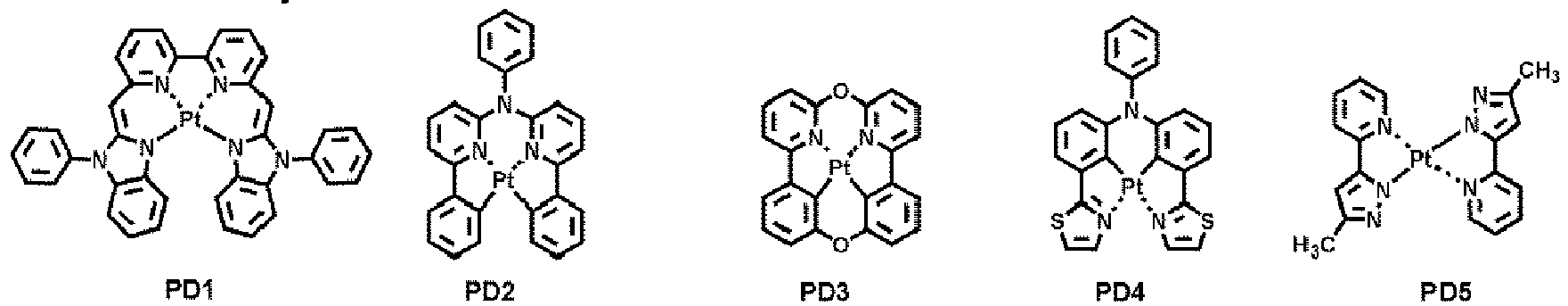


- In some embodiments, the emission layer may comprise the first compound, and when the first compound serves as an ancillary dopant, the emission layer may comprise a fluorescent dopant.
- In some embodiments, the emission layer may comprise the first compound, and when the first compound serves as a phosphorescent dopant, the emission layer may comprise an ancillary dopant.
- The fluorescent dopant and the ancillary dopant may each independently comprise an arylamine compound, a styrylamine compound, a boron-containing compound, or any combination thereof.
- In some embodiments, the fluorescent dopant and the ancillary dopant may each independently comprise the compound represented by Formula 501:

Ar501, L501 to L503, R501, and R502 may each independently be a C3-C60 carbocyclic group unsubstituted or substituted with at least one R10a or a C1-C60 heterocyclic group unsubstituted or substituted with at least one R10a,
xd1 to xd3 may each independently be 0, 1, 2, or 3, and
xd4 may be 1, 2, 3, 4, 5, or 6. - In some embodiments, in Formula 501, Ar501 may comprise a condensed ring group (e.g., an anthracene group, a chrysene group, and/or a pyrene group), in which at least three monocyclic groups are condensed.
- In some embodiments, xd4 in Formula 501 may be 2.
- In some embodiments, the fluorescent dopant and the ancillary dopant may each independently comprise one of Compounds FD1 to FD36, DPVBi, DPAVBi, or any combination thereof:


- In some embodiments, the fluorescent dopant and the ancillary dopant may each independently comprise the fourth compound represented by Formula 502 or Formula 503.
- The electron transport region may have i) a single-layered structure comprising (e.g., consisting of) a single layer comprising (e.g., consisting of) a single material, ii) a single-layered structure comprising (e.g., consisting of) a single layer comprising a plurality of different materials, or iii) a multi-layered structure having a plurality of layers comprising a plurality of different materials.
- The electron transport region may comprise a buffer layer, a hole blocking layer, an electron control layer, an electron transport layer, or an electron injection layer.
- In some embodiments, the electron transport region may have an electron transport layer/electron injection layer structure, a hole blocking layer/electron transport layer/electron injection layer structure, an electron control layer/electron transport layer/electron injection layer structure, or a buffer layer/electron transport layer/electron injection layer structure, wherein layers of each structure are sequentially stacked on the emission layer in each stated order.
- The electron transport region (e.g., a buffer layer, a hole blocking layer, an electron control layer, and/or an electron transport layer in the electron transport region) may comprise a metal-free compound comprising at least one π electron-deficient nitrogen-containing C1-C60 cyclic group.
- In some embodiments, the electron transport region may comprise a compound represented by Formula 601:
Formula 601 [Ar601]xe11-[(L601)xe1-R601]xe21,
wherein, in Formula 601,
Ar601 and L601 may each independently be a C3-C60 carbocyclic group unsubstituted or substituted with at least one R10a or a C1-C60 heterocyclic group unsubstituted or substituted with at least one R10a,
xe11 may be 1, 2, or 3,
xe1 may be 0, 1, 2, 3, 4, or 5,
R601 may be a C3-C60 carbocyclic group unsubstituted or substituted with at least one R10a, a C1-C60 heterocyclic group unsubstituted or substituted with at least one R10a, -Si(Q601)(Q602)(Q603), -C(=O)(Q601), -S(=O)2(Q601), or -P(=O)(Q601)(Q602),
Q601 to Q603 may each be understood by referring to the description of Q1 provided herein,
xe21 may be 1, 2, 3, 4, or 5, and
at least one of Ar601, L601, and R601 may each independently be a π electron-deficient nitrogen-containing C1-C60 cyclic group unsubstituted or substituted with at least one R10a. - In some embodiments, when xe11 in Formula 601 is 2 or greater, at least two Ar601(s) may be bound via a single bond.
- In some embodiments, in Formula 601, Ar601 may be a substituted or unsubstituted anthracene group.
- In some embodiments, the electron transport region may comprise a compound represented by Formula 601-1:

X614 may be N or C(R614), X615 may be N or C(R615), X616 may be N or C(R616), at least one selected from X614 to X616 may be N,
L611 to L613 may each be understood by referring to the description of L601 provided herein,
xe611 to xe613 may each be understood by referring to the description of xe1 provided herein,
R611 to R613 may each be understood by referring to the description of R601 provided herein, and
R614 to R616 may each independently be hydrogen, deuterium, -F, -CI, -Br, -I, a hydroxyl group, a cyano group, a nitro group, a C1-C20 alkyl group, a C1-C20 alkoxy group, a C3-C60 carbocyclic group unsubstituted or substituted with at least one R10a, or a C1-C60 heterocyclic group unsubstituted or substituted with at least one R10a. - For example, in Formulae 601 and 601-1, xe1 and xe611 to xe613 may each independently be 0, 1, or 2.
- The electron transport region may comprise one of Compounds ET1 to ET45, 2,9-dimethyl-4,7-diphenyl-1,10-phenanthroline (BCP), 4,7-diphenyl-1,10-phenanthroline (Bphen), Alq3, BAIq, TAZ, NTAZ, or any combination thereof:


- The thickness of the electron transport region may be in a range of about 100 Å to about 5,000 Å, and in some embodiments, about 160 Å to about 4,000 Å. When the electron transport region comprises a buffer layer, a hole blocking layer, an electron control layer, an electron transport layer, or any combination thereof, the thicknesses of the buffer layer, the hole blocking layer, or the electron control layer may each independently be in a range of about 20 Å to about 1,000 Å, for example, about 30 Å to about 300 Å, and the thickness of the electron transport layer may be in a range of about 100 Å to about 1,000 Å, for example, about 150 Å to about 500 Å. When the thicknesses of the buffer layer, the hole blocking layer, the electron control layer, and/or the electron transport layer are each within their respective ranges, excellent (or improved) hole transport characteristics may be obtained without a substantial increase in driving voltage.
- The electron transport region (for example, the electron transport layer in the electron transport region) may further comprise, in addition to the materials described above, a metal-containing material.
- The metal-containing material may comprise an alkali metal complex, an alkaline earth metal complex, or any combination thereof. A metal ion of the alkali metal complex may be a lithium (Li) ion, a sodium (Na) ion, a potassium (K) ion, a rubidium (Rb) ion, or a cesium (Cs) ion. A metal ion of the alkaline earth metal complex may be a beryllium (Be) ion, a magnesium (Mg) ion, a calcium (Ca) ion, a strontium (Sr) ion, or a barium (Ba) ion. Ligand coordinated with the metal ion of the alkali metal complex and the alkaline earth metal complex may each independently be hydroxyquinoline, hydroxyisoquinoline, hydroxybenzoquinoline, hydroxyacridine, hydroxyphenanthridine, hydroxyphenyloxazole, hydroxyphenylthiazole, hydroxyphenyloxadiazole, hydroxyphenylthiadiazole, hydroxyphenylpyridine, hydroxyphenylbenzimidazole, hydroxyphenylbenzothiazole, bipyridine, phenanthroline, cyclopentadiene, or any combination thereof.
- For example, the metal-containing material may comprise a Li complex. The Li complex may comprise, e.g., Compound ET-D1 (LiQ) and/or Compound ET-D2:

- The electron transport region may comprise an electron injection layer that facilitates injection of electrons from the
second electrode 150. The electron injection layer may be in direct contact with thesecond electrode 150. - The electron injection layer may have i) a single-layered structure comprising (e.g., consisting of) a single layer comprising (e.g., consisting of) a single material, ii) a single-layered structure comprising (e.g., consisting of) a single layer comprising a plurality of different materials, or iii) a multi-layered structure having a plurality of layers comprising a plurality of different materials.
- The electron injection layer may comprise an alkali metal, an alkaline earth metal, a rare earth metal, an alkali metal-containing compound, an alkaline earth metal-containing compound, a rare earth metal-containing compound, an alkali metal complex, an alkaline earth metal complex, a rare earth metal complex, or any combination thereof.
- The alkali metal may be Li, Na, K, Rb, Cs or any combination thereof. The alkaline earth metal may be Mg, Ca, Sr, Ba, or any combination thereof. The rare earth metal may be Sc, Y, Ce, Tb, Yb, Gd, or any combination thereof.
- The alkali metal-containing compound, the alkaline earth metal-containing compound, and the rare earth metal-containing compound may respectively be oxides, halides (e.g., fluorides, chlorides, bromides, and/or iodines), tellurides, or any combination thereof of the alkali metal, the alkaline earth metal, and the rare earth metal.
- The alkali metal-containing compound may be selected from alkali metal oxides (such as Li2O, Cs2O, and/or K2O), alkali metal halides (such as LiF, NaF, CsF, KF, Lil, Nal, Csl, and/or KI), or any combination thereof. The alkaline earth-metal-containing compound may comprise alkaline earth-metal oxides (such as BaO, SrO, CaO, BaxSr1-xO (wherein x is a real number satisfying 0<x<1), and/or BaxCa1-xO (wherein x is a real number satisfying 0<x<1)). The rare earth metal-containing compound may comprise YbF3, ScF3, Sc2O3, Y2O3, Ce2O3, GdF3, TbF3, YbI3, ScI3, TbI3, or any combination thereof. In some embodiments, the rare earth metal-containing compound may comprise a lanthanide metal telluride. Non-limiting examples of the lanthanide metal telluride may comprise LaTe, CeTe, PrTe, NdTe, PmTe, SmTe, EuTe, GdTe, TbTe, DyTe, HoTe, ErTe, TmTe, YbTe, LuTe, La2Te3, Ce2Te3, Pr2Te3, Nd2Te3, Pm2Te3, Sm2Te3, Eu2Te3, Gd2Te3, Tb2Te3, Dy2Te3, Ho2Te3, Er2Te3, Tm2Te3, Yb2Te3, Lu2Te3, and the like.
- The alkali metal complex, the alkaline earth metal complex, and the rare earth metal complex may respectively comprise: i) one of metal ions of the alkali metal, alkaline earth metal, and rare earth metal described above and ii) a ligand bound to the metal ion, e.g., hydroxyquinoline, hydroxyisoquinoline, hydroxybenzoquinoline, hydroxyacridine, hydroxyphenanthridine, hydroxyphenyloxazole, hydroxyphenylthiazole, hydroxyphenyloxadiazole, hydroxyphenylthiadiazole, hydroxyphenylpyridine, hydroxyphenylbenzimidazole, hydroxyphenylbenzothiazole, bipyridine, phenanthroline, cyclopentadiene, or any combination thereof.
- The electron injection layer may comprise (e.g., consist of) an alkali metal, an alkaline earth metal, a rare earth metal, an alkali metal-containing compound, an alkaline earth metal-containing compound, a rare earth metal-containing compound, an alkali metal complex, an alkaline earth metal complex, a rare earth metal complex, or any combination thereof, as described above. In some embodiments, the electron injection layer may further comprise an organic material (e.g., a compound represented by Formula 601).
- In some embodiments, the electron injection layer may comprise (e.g., consist of) i) an alkali metal-containing compound (e.g., alkali metal halide), or ii) a) an alkali metal-containing compound (e.g., alkali metal halide); and b) an alkali metal, an alkaline earth metal, a rare earth metal, or any combination thereof. In some embodiments, the electron injection layer may be a KI:Yb co-deposition layer, a Rbl:Yb co-deposition layer, and/or the like.
- When the electron injection layer further comprises an organic material, the alkali metal, the alkaline earth metal, the rare earth metal, the alkali metal-containing compound, the alkaline earth metal-containing compound, the rare earth metal-containing compound, the alkali metal complex, the alkaline earth metal complex, the rare earth metal complex, or any combination thereof may be homogeneously or non-homogeneously dispersed in a matrix comprising the organic material.
- The thickness of the electron injection layer may be in a range of about 1 Å to about 100 Å, and in some embodiments, about 3 Å to about 90 Å. When the thickness of the electron injection layer is within any of these ranges, excellent (or improved) electron injection characteristics may be obtained without a substantial increase in driving voltage.
- The
second electrode 150 may be on theinterlayer 130. In one or more embodiments, thesecond electrode 150 may be a cathode, that is an electron injection electrode. In this embodiment, a material for forming thesecond electrode 150 may be a material having a low work function, for example, a metal, an alloy, an electrically conductive compound, or any combination thereof. - The
second electrode 150 may comprise lithium (Li), silver (Ag), magnesium (Mg), aluminum (Al), aluminum-lithium (Al-Li), calcium (Ca), magnesium-indium (Mg-In), magnesium-silver (Mg-Ag), ytterbium (Yb), silver-ytterbium (Ag-Yb), ITO, IZO, or any combination thereof. Thesecond electrode 150 may be a transmissive electrode, a semi-transmissive electrode, or a reflective electrode.
Thesecond electrode 150 may have a single-layered structure, or a multi-layered structure comprising two or more layers. - A first capping layer may be located outside the
first electrode 110, and/or a second capping layer may be located outside thesecond electrode 150. In some embodiments, the light-emittingdevice 10 may have a structure in which the first capping layer, thefirst electrode 110, theinterlayer 130, and thesecond electrode 150 are sequentially stacked in this stated order, a structure in which thefirst electrode 110, theinterlayer 130, thesecond electrode 150, and the second capping layer are sequentially stacked in this stated order, or a structure in which the first capping layer, thefirst electrode 110, theinterlayer 130, thesecond electrode 150, and the second capping layer are sequentially stacked in this stated order. - In the light-emitting
device 10, light emitted from the emission layer in theinterlayer 130 may pass through the first electrode 110 (which may be a semi-transmissive electrode or a transmissive electrode) and through the first capping layer to the outside. In the light-emittingdevice 10, light emitted from the emission layer in theinterlayer 130 may pass through the second electrode 150 (which may be a semi-transmissive electrode or a transmissive electrode) and through the second capping layer to the outside. - The first capping layer and the second capping layer may improve the external luminescence efficiency based on the principle of constructive interference. Accordingly, the optical extraction efficiency of the light-emitting
device 10 may be increased, thus improving luminescence efficiency of the light-emittingdevice 10. - The first capping layer and the second capping layer may each comprise a material having a refractive index of 1.6 or higher (at 589 nm).
- The first capping layer and the second capping layer may each independently be a capping layer comprising an organic material, an inorganic capping layer comprising an inorganic material, or a composite capping layer comprising an organic material and an inorganic material.
- At least one of the first capping layer and the second capping layer may each independently comprise one or more selected from carbocyclic compounds, heterocyclic compounds, amine group-containing compounds, porphine derivatives, phthalocyanine derivatives, naphthalocyanine derivatives, alkali metal complexes, alkaline earth metal complexes, and any combinations thereof. The carbocyclic compound, the heterocyclic compound, and the amine group-containing compound may optionally be substituted with a substituent containing O, N, S, Se, Si, F, Cl, Br, I, or any combination thereof. In some embodiments, at least one of the first capping layer and the second capping layer may each independently comprise an amine group-containing compound.
- In some embodiments, at least one of the first capping layer and the second capping layer may each independently comprise the compound represented by Formula 201, the compound represented by Formula 202, or any combination thereof.
- In one or more embodiments, at least one of the first capping layer and the second capping layer may each independently comprise one of Compounds HT28 to HT33, one of Compounds CP1 to CP6, β-NPB, or any combination thereof:


- The light-emitting device may be comprised in various suitable electronic apparatuses. In some embodiments, an electronic apparatus comprising the light-emitting device may be an emission apparatus or an authentication apparatus.
- The electronic apparatus (e.g., an emission apparatus) may further comprise, in addition to the light-emitting device, i) a color filter, ii) a color-conversion layer, or iii) a color filter and a color-conversion layer. The color filter and/or the color-conversion layer may be disposed on at least one traveling direction of light emitted from the light-emitting device. For example, light emitted from the light-emitting device may be blue light or white light. The light-emitting device may be understood by referring to the description thereof provided herein. In some embodiments, the color-conversion layer may comprise quantum dots.
- The electronic apparatus may comprise a first substrate. The first substrate may comprise a plurality of sub-pixel areas, the color filter may comprise a plurality of color filter areas respectively corresponding to the plurality of sub-pixel areas, and the color-conversion layer may comprise a plurality of color-conversion areas respectively corresponding to the plurality of sub-pixel areas.
- A pixel defining film may be located between the plurality of sub-pixel areas to define each sub-pixel area.
- The color filter may further comprise a plurality of color filter areas and light-blocking patterns between the plurality of color filter areas, and the color-conversion layer may further comprise a plurality of color-conversion areas and light-blocking patterns between the plurality of color-conversion areas.
- The plurality of color filter areas (and/or a plurality of color-conversion areas) may comprise: a first area to emit first color light; a second area to emit second color light; and/or a third area to emit third color light, and the first color light, the second color light, and/or the third color light may have different maximum emission wavelengths. In some embodiments, the first color light may be red light, the second color light may be green light, and the third color light may be blue light. In some embodiments, the plurality of color filter areas (and/or the plurality of color-conversion areas) may each comprise quantum dots. In some embodiments, the first area may comprise red quantum dots, the second area may comprise green quantum dots, and the third area may not comprise a quantum dot. The quantum dot may be understood by referring to the description of the quantum dot provided herein. The first area, the second area, and/or the third area may each further comprise an emitter.
- In some embodiments, the light-emitting device may emit first light, the first area may absorb the first light to emit 1-1 color light, the second area may absorb the first light to emit 2-1 color light, and the third area may absorb the first light to emit 3-1 color light. In this embodiment, the 1-1 color light, the 2-1 color light, and the 3-1 color light may each have a different maximum emission wavelength. In some embodiments, the first light may be blue light, the 1-1 color light may be red light, the 2-1 color light may be green light, and the 3-1 color light may be blue light.
- The electronic apparatus may further comprise a thin-film transistor, in addition to the light-emitting device. The thin-film transistor may comprise a source electrode, a drain electrode, and an active layer, wherein one of the source electrode or the drain electrode may be electrically connected to one of the first electrode or the second electrode of the light-emitting device.
- The thin-film transistor may further comprise a gate electrode, a gate insulating film, and/or the like.
- The active layer may comprise a crystalline silicon, an amorphous silicon, an organic semiconductor, and/or an oxide semiconductor.
- The electronic apparatus may further comprise an encapsulation unit for sealing the light-emitting device. The encapsulation unit may be located between the color filter and/or the color-conversion layer and the light-emitting device. The encapsulation unit may allow light to pass to the outside from the light-emitting device and may prevent or reduce the permeation of the air and moisture into the light-emitting device at the same time. The encapsulation unit may be a sealing substrate comprising a transparent glass and/or a plastic substrate. The encapsulation unit may be a thin-film encapsulating layer comprising at least one of an organic layer or an inorganic layer. When the encapsulation unit is a thin film encapsulating layer, the electronic apparatus may be flexible.
- In addition to the color filter and/or the color-conversion layer, one or more functional layers may be disposed on the encapsulation unit, depending on the use of an electronic apparatus. Examples of the functional layer may comprise a touch screen layer, a polarization layer, and the like. The touch screen layer may be a resistive touch screen layer, a capacitive touch screen layer, or an infrared beam touch screen layer. The authentication apparatus may be, for example, a biometric authentication apparatus that identifies an individual according biometric information (e.g., a fingertip, a pupil, and/or the like).
- The authentication apparatus may further comprise a biometric information collecting unit, in addition to the light-emitting device described above.
- The electronic apparatus may be applicable to various suitable displays, an optical source, lighting, a personal computer (e.g., a mobile personal computer), a cellphone, a digital camera, an electronic note, an electronic dictionary, an electronic game console, a medical device (e.g., an electronic thermometer, a blood pressure meter, a glucometer, a pulse measuring device, a pulse wave measuring device, an electrocardiograph recorder, an ultrasonic diagnosis device, an endoscope display device), a fish finder, various measurement devices, gauges (e.g., gauges of an automobile, an airplane, a ship), a projector, and/or the like.
-
FIG. 2 is a schematic cross-sectional view of a light-emitting apparatus according to one or more embodiments. - An emission apparatus in
FIG. 2 may comprise asubstrate 100, a thin-film transistor, a light-emitting device, and anencapsulation unit 300 sealing the light-emitting device. - The
substrate 100 may be a flexible substrate, a glass substrate, or a metal substrate. Abuffer layer 210 may be on thesubstrate 100. Thebuffer layer 210 may prevent or reduce penetration of impurities through thesubstrate 100, and may provide a flat surface on thesubstrate 100. - A thin-film transistor may be on the
buffer layer 210. The thin-film transistor may comprise anactive layer 220, agate electrode 240, asource electrode 260, and adrain electrode 270. - The
active layer 220 may comprise an inorganic semiconductor (such as silicon and/or polysilicon), an organic semiconductor, or an oxide semiconductor, and may comprise a source area, a drain area and a channel area. - A
gate insulating film 230 for insulating theactive layer 220 and thegate electrode 240 may be on theactive layer 220, and thegate electrode 240 may be on thegate insulating film 230. - An interlayer insulating
film 250 may be on thegate electrode 240. Theinterlayer insulating film 250 may be between thegate electrode 240 and thesource electrode 260, and between thegate electrode 240 and thedrain electrode 270 to provide insulation therebetween. - The
source electrode 260 and thedrain electrode 270 may be on theinterlayer insulating film 250. Theinterlayer insulating film 250 and thegate insulating film 230 may be formed to expose the source area and the drain area of theactive layer 220, and thesource electrode 260 and thedrain electrode 270 may be adjacent to the exposed source area and the exposed drain area of theactive layer 220. - Such a thin-film transistor may be electrically connected to a light-emitting device to drive the light-emitting device, and may be protected by a
passivation layer 280. Thepassivation layer 280 may comprise an inorganic insulating film, an organic insulating film, or a combination thereof. A light-emitting device may be on thepassivation layer 280. The light-emitting device may comprise afirst electrode 110, aninterlayer 130, and asecond electrode 150. - The
first electrode 110 may be on thepassivation layer 280. Thepassivation layer 280 may not fully cover thedrain electrode 270, and may expose a specific (or set) area of thedrain electrode 270, and thefirst electrode 110 may be disposed to connect to (e.g., to contact) the exposed area of thedrain electrode 270. - A pixel-defining
film 290 may be on thefirst electrode 110. The pixel-definingfilm 290 may expose a specific (or set) area of thefirst electrode 110, and theinterlayer 130 may be formed in the exposed area. The pixel-definingfilm 290 may be a polyimide or polyacryl organic film. In one or more embodiments, some of the upper layers of theinterlayer 130 may extend to the upper portion of the pixel-definingfilm 290 and may be disposed in the form of a common layer. - The
second electrode 150 may be on theinterlayer 130, and acapping layer 170 may be additionally formed on thesecond electrode 150. Thecapping layer 170 may be formed to cover thesecond electrode 150. - The
encapsulation unit 300 may be on thecapping layer 170. Theencapsulation unit 300 may be on the light-emitting device to protect a light-emitting device from moisture and/or oxygen. Theencapsulation unit 300 may comprise: an inorganic film comprising silicon nitride (SiNx), silicon oxide (SiOx), indium tin oxide, indium zinc oxide, or any combination thereof; an organic film comprising polyethylene terephthalate, polyethylene naphthalate, polycarbonate, polyimide, polyethylene sulfonate, polyoxy methylene, polyarylate, hexamethyl disiloxane, an acrylic resin (e.g., polymethyl methacrylate, polyacrylic acid, and/or the like), an epoxy resin (e.g., aliphatic glycidyl ether (AGE) and/or the like), or any combination thereof; or a combination of the inorganic film and the organic film. -
FIG. 3 is a schematic cross-sectional view of another light-emitting apparatus according to one or more embodiments. - The emission apparatus shown in
FIG. 3 may be substantially identical to the emission apparatus shown inFIG. 2 , except that a light-shielding pattern 500 and afunctional area 400 are additionally located on theencapsulation unit 300. Thefunctional area 400 may be i) a color filter area, ii) a color-conversion area, or iii) a combination of a color filter area and a color-conversion area. In some embodiments, the light-emitting device shown inFIG. 3 comprised in the emission apparatus may be a tandem light-emitting device. - The layers constituting the hole transport region, the emission layer, and the layers constituting the electron transport region may be formed in a specific region by using one or more suitable methods selected from vacuum deposition, spin coating, casting, Langmuir-Blodgett (LB) deposition, ink-jet printing, laser printing, and laser-induced thermal imaging.
- When the layers constituting the hole transport region, the emission layer, and the layers constituting the electron transport region are each independently formed by vacuum deposition, the vacuum deposition may be performed at a deposition temperature in a range of about 100 °C to about 500 °C at a vacuum degree in a range of about 10-8 torr to about 10-3 torr, and at a deposition rate in a range of about 0.01 Angstroms per second (Å/sec) to about 100 Å/sec, depending on the material to be comprised in each layer and the structure of each layer to be formed.
- The term "C3-C60 carbocyclic group" as used herein refers to a cyclic group consisting of carbon atoms only as ring-forming atoms, and having 3 to 60 ring-forming carbon atoms. The term "C1-C60 heterocyclic group" as used herein refers to a cyclic group having 1 to 60 ring-forming carbon atoms, in addition to a heteroatom other than a carbon atom. The C3-C60 carbocyclic group and the C1-C60 heterocyclic group may each independently be a monocyclic group consisting of one ring or a polycyclic group in which at least two rings are condensed. For example, the total number of ring-forming atoms in the C1-C60 heterocyclic group may be in a range of 1 to 60.
- The term "cyclic group" as used herein may comprise the C3-C60 carbocyclic group and the C1-C60 heterocyclic group.
- The term "π electron-rich C3-C60 cyclic group" refers to a cyclic group having 3 to 60 carbon atoms and not comprising *-N=*' as a ring-forming moiety. The term "π electron-deficient nitrogen-containing C1-C60 cyclic group" as used herein refers to a heterocyclic group having 1 to 60 carbon atoms and *-N=*' as a ring-forming moiety.
- In some embodiments,
the C3-C60 carbocyclic group may be i) a T1 group or ii) a group in which at least two T1 groups are condensed (for example, the C3-C60 carbocyclic group may be a cyclopentadiene group, an adamantane group, a norbornane group, a benzene group, a pentalene group, a naphthalene group, an azulene group, an indacene group, an acenaphthylene group, a phenalene group, a phenanthrene group, an anthracene group, a fluoranthene group, a triphenylene group, a pyrene group, a chrysene group, a perylene group, a pentaphene group, a heptalene group, a naphthacene group, a picene group, a hexacene group, a pentacene group, a rubicene group, a coronene group, an ovalene group, an indene group, a fluorene group, a spiro-bifluorene group, a benzofluorene group, an indenophenanthrene group, or an indenoanthracene group),
the C1-C60 heterocyclic group may be i) a T2 group, ii) a group in which at least two T2 groups are condensed, or iii) a group in which at least one T2 group is condensed with at least one T1 group (for example, the C1-C60 heterocyclic group may be a pyrrole group, a thiophene group, a furan group, an indole group, a benzoindole group, a naphthoindole group, an isoindole group, a benzoisoindole group, a naphthoisoindole group, a benzosilole group, a benzothiophene group, a benzofuran group, a carbazole group, a dibenzosilole group, a dibenzothiophene group, a dibenzofuran group, an indenocarbazole group, an indolocarbazole group, a benzofurocarbazole group, a benzothienocarbazole group, a benzosilolocarbazole group, a benzoindolocarbazole group, a benzocarbazole group, a benzonaphthofuran group, a benzonapthothiophene group, a benzonaphthosilole group, a benzofurodibenzofuran group, a benzofurodibenzothiophene group, a benzothienodibenzothiophene group, a pyrazole group, an imidazole group, a triazole group, an oxazole group, an isoxazole group, an oxadiazole group, a thiazole group, an isothiazole group, a thiadiazole group, a benzopyrazole group, a benzimidazole group, a benzoxazole group, a benzoisoxazole group, a benzothiazole group, a benzoisothiazole group, a pyridine group, a pyrimidine group, a pyrazine group, a pyridazine group, a triazine group, a quinoline group, an isoquinoline group, a benzoquinoline group, a benzoisoquinoline group, a quinoxaline group, a benzoquinoxaline group, a quinazoline group, a benzoquinazoline group, a phenanthroline group, a cinnoline group, a phthalazine group, a naphthyridine group, an imidazopyridine group, an imidazopyrimidine group, an imidazotriazine group, an imidazopyrazine group, an imidazopyridazine group, an azacarbazole group, an azafluorene group, an azadibenzosilole group, an azadibenzothiophene group, an azadibenzofuran group, and/or the like),
the π electron-rich C3-C60 cyclic group may be i) a T1 group, ii) a condensed group in which at least two T1 groups are condensed, iii) a T3 group, iv) a condensed group in which at least two T3 groups are condensed, or v) a condensed group in which at least one T3 group is condensed with at least one T1 group (for example, the π electron-rich C3-C60 cyclic group may be a C3-C60 carbocyclic group, a pyrrole group, a thiophene group, a furan group, an indole group, a benzoindole group, a naphthoindole group, an isoindole group, a benzoisoindole group, a naphthoisoindole group, a benzosilole group, a benzothiophene group, a benzofuran group, a carbazole group, a dibenzosilole group, a dibenzothiophene group, a dibenzofuran group, an indenocarbazole group, an indolocarbazole group, a benzofurocarbazole group, a benzothienocarbazole group, a benzosilolocarbazole group, a benzoindolocarbazole group, a benzocarbazole group, a benzonaphthofuran group, a benzonapthothiophene group, a benzonaphthosilole group, a benzofurodibenzofuran group, a benzofurodibenzothiophene group, a benzothienodibenzothiophene group, and/or the like), and
the π electron-deficient nitrogen-containing C1-C60 cyclic group may be i) a T4 group, ii) a group in which at least twos T4 groups are condensed, iii) a group in which at least one T4 group is condensed with at least one T1 group, iv) a group in which at least one T4 group is condensed with at least one T3 group, or v) a group in which at least one T4 group, at least one T1 group, and at least one T3 group are condensed (for example, he π electron-deficient nitrogen-containing C1-C60 cyclic group may be a pyrazole group, an imidazole group, a triazole group, an oxazole group, an isoxazole group, an oxadiazole group, a thiazole group, an isothiazole group, a thiadiazole group, a benzopyrazole group, a benzimidazole group, a benzoxazole group, a benzoisoxazole group, a benzothiazole group, a benzoisothiazole group, a pyridine group, a pyrimidine group, a pyrazine group, a pyridazine group, a triazine group, a quinoline group, an isoquinoline group, a benzoquinoline group, a benzoisoquinoline group, a quinoxaline group, a benzoquinoxaline group, a quinazoline group, a benzoquinazoline group, a phenanthroline group, a cinnoline group, a phthalazine group, a naphthyridine group, an imidazopyridine group, an imidazopyrimidine group, an imidazotriazine group, an imidazopyrazine group, an imidazopyridazine group, an azacarbazole group, an azafluorene group, an azadibenzosilole group, an azadibenzothiophene group, an azadibenzofuran group, and/or the like),
wherein the T1 group may be a cyclopropane group, a cyclobutane group, a cyclopentane group, a cyclohexane group, a cycloheptane group, a cyclooctane group, a cyclobutene group, a cyclopentene group, a cyclopentadiene group, a cyclohexene group, a cyclohexadiene group, a cycloheptene group, an adamantane group, a norbornane (or bicyclo[2.2.1]heptane) group, a norbornene group, a bicyclo[1.1.1]pentane group, a bicyclo[2.1,1]hexane group, a bicyclo[2.2.2]octane group, or a benzene group,
the T2 group may be a furan group, a thiophene group, a 1H-pyrrole group, a silole group, a borole group, a 2H-pyrrole group, a 3H-pyrrole group, an imidazole group, a pyrazole group, a triazole group, a tetrazole group, an oxazole group, an isoxazole group, an oxadiazole group, a thiazole group, an isothiazole group, a thiadiazole group, an azasilole group, an azaborole group, a pyridine group, a pyrimidine group, a pyrazine group, a pyridazine group, a triazine group, or a tetrazine group,
the T3 group may be a furan group, a thiophene group, a 1H-pyrrole group, a silole group, or a borole group, and
the T4 group may be a 2H-pyrrole group, a 3H-pyrrole group, an imidazole group, a pyrazole group, a triazole group, a tetrazole group, an oxazole group, an isoxazole group, an oxadiazole group, a thiazole group, an isothiazole group, a thiadiazole group, an azasilole group, an azaborole group, a pyridine group, a pyrimidine group, a pyrazine group, a pyridazine group, a triazine group, or a tetrazine group. - The term "cyclic group", "C3-C60 carbocyclic group", "C1-C60 heterocyclic group", "π electron-rich C3-C60 cyclic group", or "π electron-deficient nitrogen-containing C1-C60 cyclic group" as used herein may be a group condensed with any suitable cyclic group, a monovalent group, or a polyvalent group (e.g., a divalent group, a trivalent group, a quadvalent group, and/or the like), depending on the structure of the formula to which the term is applied. For example, a "benzene group" may be a benzo group, a phenyl group, a phenylene group, and/or the like, and this may be understood by one of ordinary skill in the art, depending on the structure of the formula comprising the "benzene group".
- Examples of the monovalent C3-C60 carbocyclic group and the monovalent C1-C60 heterocyclic group may comprise a C3-C10 cycloalkyl group, a C1-C10 heterocycloalkyl group, a C3-C10 cycloalkenyl group, a C1-C10 heterocycloalkenyl group, a C6-C60 aryl group, a C1-C60 heteroaryl group, a monovalent non-aromatic condensed polycyclic group, and a monovalent non-aromatic condensed heteropolycyclic group. Examples of the divalent C3-C60 carbocyclic group and the divalent C1-C60 heterocyclic group may comprise a C3-C10 cycloalkylene group, a C1-C10 heterocycloalkylene group, a C3-C10 cycloalkenylene group, a C1-C10 heterocycloalkenylene group, a C6-C60 arylene group, a C1-C60 heteroarylene group, a divalent non-aromatic condensed polycyclic group, and a divalent non-aromatic condensed heteropolycyclic group.
- The term "C1-C60 alkyl group" as used herein refers to a linear or branched aliphatic hydrocarbon monovalent group having 1 to 60 carbon atoms, and non-limiting examples thereof comprise a methyl group, an ethyl group, an n-propyl group, an isopropyl group, an n-butyl group, a sec-butyl group, an isobutyl group, a tert-butyl group, an n-pentyl group, a tert-pentyl group, a neopentyl group, an isopentyl group, a sec-pentyl group, a 3-pentyl group, a sec-isopentyl group, an n-hexyl group, an iso-hexyl group, a sec-hexyl group, a tert-hexyl group, an n-heptyl group, an iso-heptyl group, a sec-heptyl group, a tert-heptyl group, an n-octyl group, an iso-octyl group, a sec-octyl group, a tert-octyl group, an n-nonyl group, an iso-nonyl group, a sec-nonyl group, a tert-nonyl group, an n-decyl group, an iso-decyl group, a sec-decyl group, and a tert-decyl group. The term "C1-C60 alkylene group" as used herein refers to a divalent group having the same structure as the C1-C60 alkyl group.
- The term "C2-C60 alkenyl group" as used herein refers to a hydrocarbon group having at least one carbon-carbon double bond in the middle and/or at either terminus of the C2-C60 alkyl group. Non-limiting examples thereof comprise an ethenyl group, a propenyl group, and a butenyl group. The term "C2-C60 alkenylene group" as used herein refers to a divalent group having the same structure as the C2-C60 alkenyl group.
- The term "C2-C60 alkynyl group" as used herein refers to a monovalent hydrocarbon group having at least one carbon-carbon triple bond in the middle and/or at either terminus of the C2-C60 alkyl group. Non-limiting examples thereof comprise an ethynyl group and a propynyl group. The term "C2-C60 alkynylene group" as used herein refers to a divalent group having the same structure as the C2-C60 alkynyl group.
- The term "C1-C60 alkoxy group" as used herein refers to a monovalent group represented by -OA101 (wherein A101 is a C1-C1 alkyl group). Non-limiting examples thereof comprise a methoxy group, an ethoxy group, and an isopropyloxy group.
- The term "C3-C10 cycloalkyl group" as used herein refers to a monovalent saturated hydrocarbon monocyclic group comprising 3 to 10 carbon atoms. Non-limiting examples of the C3-C10 cycloalkyl group as used herein comprise a cyclopropyl group, a cyclobutyl group, a cyclopentyl group, a cyclohexyl group, a cycloheptyl group, a cyclooctyl group, an adamantanyl group, a norbornanyl (bicyclo[2.2.1]heptyl) group, a bicyclo[1.1.1]pentyl group, a bicyclo[2.1.1]hexyl group, and/or a bicyclo[2.2.2]octyl group). The term "C3-C10 cycloalkylene group" as used herein refers to a divalent group having the same structure as the C3-C10 cycloalkyl group.
- The term "C1-C10 heterocycloalkyl group" as used herein refers to a monovalent cyclic group comprising at least one heteroatom, other than carbon atoms, as a ring-forming atom, and having 1 to 10 carbon atoms. Non-limiting examples thereof comprise a 1,2,3,4-oxatriazolidinyl group, a tetrahydrofuranyl group, and a tetrahydrothiophenyl group. The term "C1-C10 heterocycloalkylene group" as used herein refers to a divalent group having the same structure as the C1-C10 heterocycloalkyl group.
- The term "C3-C10 cycloalkenyl group" as used herein refers to a monovalent cyclic group that has 3 to 10 carbon atoms and at least one carbon-carbon double bond in its ring, and is not aromatic. Non-limiting examples thereof comprise a cyclopentenyl group, a cyclohexenyl group, and a cycloheptenyl group. The term "C3-C10 cycloalkenylene group" as used herein refers to a divalent group having the same structure as the C3-C10 cycloalkenyl group.
- The term "C1-C10 heterocycloalkenyl group" as used herein refers to a monovalent cyclic group comprising at least one heteroatom, other than carbon atoms, as a ring-forming atom, 1 to 10 carbon atoms, and at least one double bond in its ring. Non-limiting examples of the C1-C10 heterocycloalkenyl group comprise a 4,5-dihydro-1,2,3,4-oxatriazolyl group, a 2,3-dihydrofuranyl group, and a 2,3-dihydrothiophenyl group. The term "C1-C10 heterocycloalkylene group" as used herein refers to a divalent group having the same structure as the C1-C10 heterocycloalkyl group. The term "C1-C10 heterocycloalkenylene group" as used herein refers to a divalent group having the same structure as the C1-C10 heterocycloalkenyl group.
- The term "C6-C60 aryl group" as used herein refers to a monovalent group having a carbocyclic aromatic system having 6 to 6 carbon atoms. The term "C6-C60 arylene group" as used herein refers to a divalent group having the same structure as the C6-C60 aryl group. Non-limiting examples of the C6-C60 aryl group comprise a phenyl group, a pentalenyl group, a naphthyl group, an azulenyl group, an indacenyl group, an acenaphthyl group, a phenalenyl group, a phenanthrenyl group, an anthracenyl group, a fluoranthenyl group, a triphenylenyl group, a pyrenyl group, a chrysenyl group, a perylenyl group, a pentaphenyl group, a heptalenyl group, a naphthacenyl group, a picenyl group, a hexacenyl group, a pentacenyl group, a rubicenyl group, a coronenyl group, and an ovalenyl group. When the C6-C60 aryl group and the C6-C60 arylene group each independently comprise two or more rings, the respective rings may be fused.
- The term "C1-C60 heteroaryl group" as used herein refers to a monovalent group having a heterocyclic aromatic system further comprising at least one heteroatom, other than carbon atoms, as a ring-forming atom, and 1 to 60 carbon atoms. The term "C1-C60 heteroarylene group" as used herein refers to a divalent group having the same structure as the C1-C60 heteroaryl group . Non-limiting examples of the C1-C60 heteroaryl group comprise a pyridinyl group, a pyrimidinyl group, a pyrazinyl group, a pyridazinyl group, a triazinyl group, a quinolinyl group, a benzoquinolinyl group, an isoquinolinyl group, a benzoisoquinolinyl group, a quinoxalinyl group, a benzoquinoxalinyl group, a quinazolinyl group, a benzoquinazolinyl group, a cinnolinyl group, a phenanthrolinyl group, a phthalazinyl group, and a naphthyridinyl group. When the C1-C60 heteroaryl group and the C1-C60 heteroarylene group each independently comprise two or more rings, the respective rings may be fused.
- The term "monovalent non-aromatic condensed polycyclic group" as used herein refers to a monovalent group that has two or more rings condensed and only carbon atoms as ring forming atoms (e.g., 8 to 60 carbon atoms), wherein the entire molecular structure (as a whole) is non-aromatic. Non-limiting examples of the monovalent non-aromatic condensed polycyclic group comprise an indenyl group, a fluorenyl group, a spiro-bifluorenyl group, a benzofluorenyl group, an indenophenanthrenyl group, and an indenoanthracenyl group. The term "divalent non-aromatic condensed polycyclic group" as used herein refers to a divalent group having substantially the same structure as the monovalent non-aromatic condensed polycyclic group.
- The term "monovalent non-aromatic condensed heteropolycyclic group" as used herein refers to a monovalent group that has two or more condensed rings and at least one heteroatom, other than carbon atoms (e.g., 1 to 60 carbon atoms), as a ring-forming atom, wherein the entire molecular structure (as a whole) is non-aromatic. Non-limiting examples of the monovalent non-aromatic condensed heteropolycyclic group comprise a pyrrolyl group, a thiophenyl group, a furanyl group, an indolyl group, a benzoindolyl group, a naphthoindolyl group, an isoindolyl group, a benzoisoindolyl group, a naphthoisoindolyl group, a benzosilolyl group, a benzothiophenyl group, a benzofuranyl group, a carbazolyl group, a dibenzosilolyl group, a dibenzothiophenyl group, a dibenzofuranyl group, an azacarbazolyl group, an azafluorenyl group, an azadibenzosilolyl group, an azadibenzothiophenyl group, an azadibenzofuranyl group, a pyrazolyl group, an imidazolyl group, a triazolyl group, a tetrazolyl group, an oxazolyl group, an isoxazolyl group, a thiazolyl group, an isothiazolyl group, an oxadiazolyl group, a thiadiazolyl group, a benzopyrazolyl group, a benzimidazolyl group, a benzoxazolyl group, a benzothiazolyl group, a benzooxadiazolyl group, a benzothiadiazolyl group, an imidazopyridinyl group, an imidazopyrimidinyl group, an imidazotriazinyl group, an imidazopyrazinyl group, an imidazopyridazinyl group, an indenocarbazolyl group, an indolocarbazolyl group, a benzofurocarbazolyl group, a benzothienocarbazolyl group, a benzosilolocarbazolyl group, a benzoindolocarbazolyl group, a benzocarbazolyl group, a benzonaphthofuranyl group, a benzonaphthothiophenyl group, a benzonaphthosilolyl group, a benzofurodibenzofuranyl group, a benzofurodibenzothiophenyl group, and a benzothienodibenzothiophenyl group. The term "divalent non-aromatic condensed heteropolycyclic group" as used herein refers to a divalent group having substantially the same structure as the monovalent non-aromatic condensed heteropolycyclic group.
- The term "C6-C60 aryloxy group" as used herein refers to a monovalent group represented by -OA102 (wherein A102 is the C6-C60 aryl group). The term "C6-C60 arylthio group" as used herein refers to a monovalent group represented by -SA103 (wherein A103 is the C6-C60 aryl group).
- The term "R10a" as used herein may be:
- deuterium (-D), -F, -CI, -Br, -I, a hydroxyl group, a cyano group, or a nitro group;
- a C1-C60 alkyl group, a C2-C60 alkenyl group, a C2-C60 alkynyl group, or a C1-C60 alkoxy group, each independently unsubstituted or substituted with deuterium, -F, - Cl, -Br, -I, a hydroxyl group, a cyano group, a nitro group, a C3-C60 carbocyclic group, a C1-C60 heterocyclic group, a C6-C60 aryloxy group, a C6-C60 arylthio group, - Si(Q11)(Q12)(Q13), -N(Q11)(Q12), -B(Q11)(Q12), -C(=O)(Q11), -S(=O)2(Q11), - P(=O)(Q11)(Q12), or any combination thereof;
- a C3-C60 carbocyclic group, a C1-C60 heterocyclic group, a C6-C60 aryloxy group, or a C6-C60 arylthio group, each independently unsubstituted or substituted with deuterium, -F, -CI, -Br, -I, a hydroxyl group, a cyano group, a nitro group, a C1-C60 alkyl group, a C2-C60 alkenyl group, a C2-C60 alkynyl group, a C1-C60 alkoxy group, a C3-C60 carbocyclic group, a C1-C60 heterocyclic group, a C6-C60 aryloxy group, a C6-C60 arylthio group, -Si(Q21)(Q22)(Q23), -N(Q21)(Q22), -B(Q21)(Q22), -C(=O)(O21), -S(=O)2(Q21), -P(=O)(Q21)(Q22), or any combination thereof; or
- -Si(Q31)(Q32)(Q33), -N(Q31)(Q32), -B(Q31)(Q32), -C(=O)(Q31), -S(=O)2(Q31), or - P(=O)(Q31)(Q32).
- Q1 to Q3, Q11 to Q13, Q21 to Q23, and Q31 to Q33 may each independently be hydrogen; deuterium; -F; -CI; -Br; -I; a hydroxyl group; a cyano group; a nitro group; a C1-C60 alkyl group; a C2-C60 alkenyl group; a C2-C60 alkynyl group; a C1-C60 alkoxy group; or a C3-C60 carbocyclic group or a C1-C60 heterocyclic group, where, when present, each C1-C60 alkyl group; C2-C60 alkenyl group; C2-C60 alkynyl group; C1-C60 alkoxy group; C3-C60 carbocyclic group or a C1-C60 heterocyclic group is independently optionally substituted with deuterium, -F, a cyano group, a C1-C60 alkyl group, a C1-C60 alkoxy group, a phenyl group, a biphenyl group, a pyridinyl group, a pyrimidinyl group, a pyridazinyl group, a pyrazinyl group, a triazinyl group, or any combination thereof.
- The term "heteroatom" as used herein refers to any atom other than a carbon atom. Non-limiting examples of the heteroatom may comprise O, S, N, P, Si, B, Ge, Se, or any combination thereof.
- "Ph" used herein represents a phenyl group, "Me" used herein represents a methyl group, "Et" used herein represents an ethyl group, "tert-Bu" or "But" used herein represents a tert-butyl group, "OMe" used herein represents a methoxy group, and "D" as used herein represents deuterium.
- The term "biphenyl group" as used herein refers to a phenyl group substituted with at least one phenyl group. The "biphenyl group" belongs to "a substituted phenyl group" having a "C6-C60 aryl group" as a substituent.
- The term "terphenyl group" as used herein refers to a phenyl group substituted with at least one biphenyl group. The "terphenyl group" belongs to "a substituted phenyl group" having a "C6-C60 aryl group substituted with a C6-C60 aryl group" as a substituent.
- The symbols *, *' and *" as used herein, unless defined otherwise, refer to a binding site to an adjacent atom in a corresponding formula.
- Certain groups are specified herein as being substituted or unsubstituted (for example, "substituted with at least one of..."). Unless otherwise specified, when a group is substituted it is typically substituted with 1, 2, 3 or 4 substituents. For example, when a group is substituted it may substituted with 1, 2 or 3 substituents; 1 or 2 substituents; or 1 substituent. Groups which are not specified as being substituted or unsubstituted are typically unsubstituted.
- Hereinafter, compounds and a light-emitting device according to one or more embodiments will be described in more detail with reference to Synthesis Examples and Examples. The wording "B was used instead of A" used in describing Synthesis Examples means that an amount of B used was identical to an amount of A used in terms of molar equivalents.
-


- 25.0 g (70.8 mmol) of 9-(4-bromopyridin-2-yl)-2-methoxy-9H-carbazole was mixed with 700 mL of tetrahydrofuran, the temperature was lowered to -78 °C, and 39 mL of n-BuLi solution (2.0 molar (M) in hexane) was added thereto, follwed by stirring for 1 hour at the same temperature. Then, 21.3 g (141.6 mmol) of 2-adamantanone was added thereto, and the temperature was raised to room temperature, followed by stirring for 24 hours. Once the reaction was complete, a NaHCO3 solution was added thereto, and an organic layer was extracted therefrom using ethyl acetate, and the extracted organic layer was washed with saturated NaCl aqueous solution, followed by drying using sodium sulfate. The resulting product was subjected to column chromatography to thereby obtain 22.3 g (52.5 mmol) of Intermediate D6-1.
- 22.3 g (52.5 mmol) of Intermediate D6-1 and 21.0 g (157.5 mmol) of AlCl3 were stirred for 24 hours at room temperature with excess benzene in a nitrogen atmosphere. Once the reaction was complete, a NaHCO3 solution was added thereto for neutralization, and an organic layer was extracted therefrom using ethyl acetate, and the extracted organic layer was washed with saturated NaCl aqueous solution, followed by drying using sodium sulfate. The resulting product was subjected to column chromatography to thereby obtain 20.0 g (41.2 mmol) of Intermediate D6-2.
- 20.2 g (41.7 mmol) of Intermediate D6-2 was suspended in an excess hydrobromic acid solution, followed by raising the temperature to 110 °C and stirring for 24 hours. Once the reaction was complete, the temperature was lowered to room temperature, and a proper amount of NaHCO3 was added thereto for neutralization. Then, 300 mL of distilled water was added thereto, and an organic layer was extracted therefrom using ethyl acetate, and the extracted organic layer was washed using saturated sodium chloride aqueous solution, followed by drying using MgSO4. The resulting product was subjected to column chromatography to thereby obtain 18.9 g (39.5 mmol) of Intermediate D6-3.
- 15.4 g (32.7mmol) of Intermediate D6-3, 8.2 g (34.6 mmol) of 1,3-dibromobenzene, 13.9 g (65.4 mmol, 2.0 eq.) of K3PO4, 0.6 g (3.3 mmol, 0.1 eq.) of CuI, and 1.3 g (3.3 mmol) of di([1,1'-biphenyl]-2-yl)oxalamide were added to a reaction vessel, and the mixture was suspended in 80 mL of dimethyl sulfoxide, followed by raising the temperature to 160 °C and stirring for 12 hours. Once the reaction was complete, the temperature was lowered to room temperature, and 300 mL of distilled water was added thereto. Then, an organic layer was extracted therefrom using ethyl acetate, and the extracted organic layer was washed with saturated NaCl aqueous solution, followed by drying using sodium sulfate. The resulting product was subjected to column chromatography to thereby obtain 16.5 g (26.3 mmol) of Intermediate D6-4.
- 23.8 g (38.1 mmol) of Intermediate D6-4, 15.8 g (45.7 mmol) of N1 -([1,1':3',1"-terphenyl]-2'-yl-2,2",3,3",4,4",5,5",6,6"-d 10)benzene-1,2-diamine, 0.4 g (0.76 mmol, 0.02 eq.) of Pd2(dba)3, 0.6 g (1.52 mmol, 0.04 eq.) of SPhos, and 4.8 g (49.5 mmol, 1.6 eq.) of NaO t Bu were added to a reaction vessel, and the mixture was suspended in 100 mL of toluene (0.1 M), followed by raising the temperature to 120 °C and stirring for 4 hours. Once the reaction was complete, the temperature was lowered to room temperature, and 300 mL of distilled water was added thereto. Then, an organic layer was extracted therefrom using ethyl acetate, and the extracted organic layer was washed with saturated NaCl aqueous solution, followed by drying using sodium sulfate. The resulting product was subjected to column chromatography to thereby obtain 23.6 g (26.5 mmol) of Intermediate D6-5.
- 23.2 g (26.0 mmol) of Intermediate D6-5, 216 mL (1.3 mol, 50.0 eq.) of triethyl orthoformate, and 0.9 mL (31.2 mmol, 1.2 eq.) of HCI (37 %) were added to a reaction vessel, and the temperature was raised to 80 °C and stirred for 12 hours. Once the reaction was complete, the temperature was cooled to room temperature, and the resulting solid was filtered and washed using ether. Then, the washed solid was dried to thereby obtain 22.5 g (23.4 mmol) of Intermediate D6-6.
- 21.1 g (22.5 mmol) of Intermediate D6-6 and 11.0 g (67.5 mmol, 3.0 eq.) of NH4PF6 were added to a reaction vessel, and the mixture was suspended in a mixed solution of 100 mL of methyl alcohol and 50 mL of water (at a volumetric ratio of 2:1), followed by stirring at room temperature for 24 hours. Once the reaction was complete, the resulting solid was filtered and washed using ether. Then, the washed solid was dried to thereby obtain 26.0 g (16.8 mmol) of Intermediate D6-7.
- 16.5 g (15.8 mmol) of Intermediate D6-7, 6.2 g (16.7 mmol, 1.1 eq.) of dichloro(1,5-cyclooctadiene)platinum, and 3.9 g (47.4 mmol, 3.0 eq.) of NaOAc were suspended in 300 mL of 1,4-dioxane (0.025 M), and the temperature was raised to 110 °C, followed by stirrring for 72 hours. Once the reaction was complete, the temperature was cooled to room temperature, 250 mL of distilled water was added thereto, and an organic layer was extracted therefrom using ethyl acetate, and the extracted organic layer was washed using NaCl aqueous solution and dried using MgSO4. The resulting product was subjected to column chromatography to thereby obtain 5.5 g (5.1 mmol) of Compound D6.
-


- 22.3 g (52.5 mmol) of Intermediate D6-1, 21.0 g (157.5 mmol) of AlCl3, and 4a,8a-azaboranaphthalene (1.0 eq.) were stirred for 24 hours at a temperature of 40 °C with excess dichloromethane in a nitrogen atmosphere. Once the reaction was complete, a NaHCO3 solution was added thereto for neutralization, and an organic layer was extracted therefrom using ethyl acetate, and the extracted organic layer was washed with saturated NaCl aqueous solution, followed by drying using sodium sulfate. The resulting product was subjected to column chromatography to thereby obtain Intermediate D12-2.
- Intermediate D12-3 was obtained in substantially the same manner as in Synthesis of Intermediate D6-3 in Synthesis Example 1, except that Intermediate D12-2 was used instead of Intermediate D6-2.
- Intermediate D12-4 was obtained in substantially the same manner as in Synthesis of Intermediate D6-4 in Synthesis Example 1, except that Intermediate D12-3 was used instead of Intermediate D6-3.
- Intermediate D12-5 was obtained in substantially the same manner as in Synthesis of Intermediate D6-5 in Synthesis Example 1, except that Intermediate D12-4 was used instead of Intermediate D6-4.
- Intermediate D12-6 was obtained in substantially the same manner as in Synthesis of Intermediate D6-6 in Synthesis Example 1, except that Intermediate D12-5 was used instead of Intermediate D6-5.
- Intermediate D12-7 was obtained in substantially the same manner as in Synthesis of Intermediate D6-7 in Synthesis Example 1, except that Intermediate D12-6 was used instead of Intermediate D6-6.
- 5.60 g (4.90 mmol) of Compound D12 was obtained in substantially the same manner as in Synthesis of Compound D6 in Synthesis Example 1, except that Intermediate D12-7 was used instead of Intermediate D6-7.
-

- Intermediate D27-4 was synthesized in substantially the same manner as in Synthesis of Intermediate D12-4 in Synthesis Example 2, except that 1,3-dibromo-5-(tert-butyl)benzene was used instead of 1,3-dibromobenzene.
- Intermediate D27-5 was obtained in substantially the same manner as in Synthesis of Intermediate D12-5 in Synthesis Example 2, except that Intermediate D27-4 was used instead of Intermediate D12-4.
- Intermediate D27-6 was obtained in substantially the same manner as in Synthesis of Intermediate D12-6 in Synthesis Example 2, except that Intermediate D27-5 was used instead of Intermediate D12-5.
- Intermediate D27-7 was obtained in substantially the same manner as in Synthesis of Intermediate D12-7 in Synthesis Example 2, except that Intermediate D27-6 was used instead of Intermediate D12-6.
- 5.88 g (4.90 mmol) of Compound D27 was obtained in substantially the same manner as in Synthesis of Compound D12 in Synthesis Example 2, except that Intermediate D27-7 was used instead of Intermediate D12-7.
-

- Intermediate D81-4 was synthesized in substantially the same manner as in Synthesis of Intermediate D6-4 in Synthesis Example 1, except that 3,5-dibromo-6'-phenyl-1,1':2',1"-terphenyl was used instead of 1,3-dibromobenzene.
- Intermediate D81-5 was obtained in substantially the same manner as in Synthesis of Intermediate D6-5 in Synthesis Example 1, except that Intermediate D81-4 was used instead of Intermediate D6-4.
- Intermediate D81-6 was obtained in substantially the same manner as in Synthesis of Intermediate D6-6 in Synthesis Example 1, except that Intermediate D81-5 was used instead of Intermediate D6-5.
- Intermediate D81-7 was obtained in substantially the same manner as in Synthesis of Intermediate D6-7 in Synthesis Example 1, except that Intermediate D81-6 was used instead of Intermediate D6-6.
- 5.22 g (3.95 mmol) of Compound D81 was obtained in substantially the same manner as in Synthesis of Compound D6 in Synthesis Example 1, except that Intermediate D81-7 was used instead of Intermediate D6-7.
-

- Intermediate D302-1 was synthesized in substantially the same manner as in Synthesis of Intermediate D6-1 in Synthesis Example 1, except that acetone-d6 was used instead of 2-adamantanone.
- Intermediate D302-2 was obtained in substantially the same manner as in Synthesis of Intermediate D6-2 in Synthesis Example 1, except that Intermediate D302-1 was used instead of Intermediate D6-1.
- Intermediate D302-3 was obtained in substantially the same manner as in Synthesis of Intermediate D6-3 in Synthesis Example 1, except that Intermediate D302-2 was used instead of Intermediate D6-2.
- Intermediate D302-4 was obtained in substantially the same manner as in Synthesis of Intermediate D6-4 in Synthesis Example 1, except that Intermediate D302-3 was used instead of Intermediate D6-3.
- Intermediate D302-5 was obtained in substantially the same manner as in Synthesis of Intermediate D6-5 in Synthesis Example 1, except that Intermediate D302-4 was used instead of Intermediate D6-4.
- Intermediate D302-6 was obtained in substantially the same manner as in Synthesis of Intermediate D6-6 in Synthesis Example 1, except that Intermediate D302-5 was used instead of Intermediate D6-5.
- Intermediate D302-7 was obtained in substantially the same manner as in Synthesis of Intermediate D6-7 in Synthesis Example 1, except that Intermediate D302-6 was used instead of Intermediate D6-6.
- 5.73 g (5.69 mmol) of Compound D302 was obtained in substantially the same manner as in Synthesis of Compound D6 in Synthesis Example 1, except that Intermediate D302-7 was used instead of Intermediate D6-7.
- Compounds synthesized in the Synthesis Examples 1 to 5 were identified by 1H nuclear magnetic resonance (NMR) and matrix-assisted laser desorption/ionization mass spectrometry time-of-flight mass spectroscopy (MALDI-TOF MS). The results thereof are shown in Table 1. Methods of synthesizing compounds other than the compounds synthesized in Synthesis Examples 1 to 5 may be easily understood by those skilled in the art by referring to the synthesis pathways and raw materials described above.
Table 1 Compound 1H NMR (CDCl3, 500 MHz) MALDI-TOF MS [M+] found calc. D6 δ 8.87 (d, 1H, 3JH-H = 6.4 Hz), 8.10 (d, 1H, 3JH-H = 7.1 Hz), 8.04 (s, 1H), 7.96 (d, 1H, 3JH-H = 8.3 Hz), 7.92 (d, 1H, 3JH-H = 8.1 Hz), 7.76 (d, 1H, 3JH-H = 8.3 Hz), 7.56 (td, 1H, 3JH-H = 7.1 Hz, 4JH-H = 1.1 Hz), 7.46-7.43 (m, 6H), 7.29 (d, 1H, 3JH-H = 8.2 Hz), 7.23-7.20 (m 6H), 7.05-7.00 (m, 2H), 6.84 (d, 1H, 3JH-H = 8.0 Hz), 6.23 (d, 1H, 3JH-H = 5.0 Hz), 3.04 (m, 2H), 1.98-1.69 (m, 12H). 1093.43 1093.41 D12 δ 8.88 (d, 1H, 3JH-H = 6.4 Hz), 8.10-8.08 (m, 2H), 8.02 (s, 1H), 7.96 (d, 1H, 3JH-H = 8.3 Hz), 7.94-7.92 (m, 2H) 7.83-7.77 (m, 2H), 7.76 (d, 1H, 3JH-H = 8.3 Hz), 7.56 (td, 1H, 3JH-H = 7.1 Hz, 4JH-H = 1.1 Hz), 7.46-7.43 (m, 3H), 7.29 (d, 1H, 3JH-H = 8.2 Hz), 7.23-7.20 (m, 5H), 7.05-7.00 (m, 2H), 6.84 (d, 1H, 3JH-H = 8.0 Hz), 6.83-6.81 (m, 2H), 6.23 (d, 1H, 3JH-H = 5.0 Hz), 3.05 (m, 2H), 1.98-1.69 (m, 12H). 1144.47 1144.44 D27 δ 8.87 (d, 1H, 3JH-H = 6.4 Hz), 8.11-8.07 (m, 2H), 8.03 (s, 1H), 7.94 (d, 1H, 3JH-H = 8.3 Hz), 7.93-7.91 (m, 2H) 7.83-7.77 (m, 2H), 7.75 (d, 1H, 3JH-H = 8.3 Hz), 7.54 (td, 1H, 3JH-H = 7.1 Hz, 4JH-H = 1.1 Hz), 7.47-7.43 (m, 2H), 7.28 (d, 1H, 3JH-H = 8.2 Hz), 7.23-7.18 (m, 5H), 7.04-7.01 (m, 2H), 6.85 (d, 1H, 3JH-H = 8.0 Hz), 6.84-6.82 (m, 2H), 6.24 (d, 1H, 3JH-H = 5.0 Hz), 3.04 (m, 2H), 1.98-1.69 (m, 12H), 1.32 (s, 9H). 1200.52 1200.50 D81 δ 8.86 (d, 1H, 3JH-H = 6.4 Hz), 8.11 (d, 1H, 3JH-H = 7.1 Hz), 8.02 (s, 1H), 7.94 (d, 1H, 3JH-H = 8.3 Hz), 7.90 (d, 1H, 3JH-H = 8.1 Hz), 7.76 (d, 1H, 3JH-H = 8.3 Hz), 7.50-7.43 (m, 11H), 7.30 (d, 1H, 3JH-H = 8.2 Hz), 7.23-7.20 (m 14H), 7.04-7.01 (m, 2H), 6.83 (d, 1H, 3JH-H = 8.0 Hz), 6.22 (d, 1H, 3JH-H = 5.0 Hz), 3.03 (m, 2H), 1.98-1.68 (m, 12H). 1321.51 1321.50 D302 δ 8.88 (d, 1H, 3JH-H = 6.4 Hz), 8.04 (d, 1H, 3JH-H = 7.7 Hz, 4JH-H = 1.3 Hz), 7.98 (d, 1H, 3JH-H = 8.3 Hz), 7.89 (d, 1H, 4JH-H = 1.8 Hz), 7.74 (d, 1H, 3JH-H = 8.2 Hz), 7.67 (d, 1H, 3JH-H = 7.6 Hz), 7.48 (d, 1H, 3JH-H = 7.6 Hz, 4JH-H = 0.8 Hz), 7.44-7.40 (m, 4H), 7.36-7.20 (m, 10H), 7.07 (d, 1H, 3JH-H = 8.1 Hz, 4JH-H = 0.8 Hz), 7.05 (td, 1H, 3JH-H = 8.1 Hz, 4JH-H = 0.8 Hz), 6.87 (d, 1H, 3JH-H = 7.8 Hz). 1007.43 1007.39 - HOMO and LUMO energy levels of Compounds D6, D12, D27, D81, and D302 were evaluated according to the method in Table 2. The results thereof are shown in Table 3.
Table 2 HOMO energy level evaluation method A potential (V)-current (A) graph of each compound was obtained by using cyclic voltammetry (CV) (electrolyte: 0.1 M BBu4NPF6/ solvent: dimethylforamide (DMF)/ electrode: 3 electrode system (working electrode: GC, reference electrode: Ag/AgCl, auxiliary electrode: Pt)), and then, from oxidation onset of the graph, a HOMO energy level of the compound was calculated. LUMO energy level evaluation method A potential (V)-current (A) graph of each compound was obtained by using cyclic voltammetry (CV) (electrolyte: 0.1 M BBu4NPF6/ solvent: dimethylforamide (DMF)/ electrode: 3 electrode system (working electrode: GC, reference electrode: Ag/AgCl, auxiliary electrode: Pt)), and then, from reduction onset of the graph, a LUMO energy level of the compound was calculated. Table 3 Compound No. HOMO (eV) LUMO (eV) D6 -5.26 -2.09 D12 -5.22 -2.22 D27 -5.23 -2.24 D81 -5.25 -2.25 D302 -5.26 -2.14 
-
Film 1 having a thickness of 40 nm was prepared by vacuum-co-depositing ETH66, HTH29, and D6 on a quartz substrate at a vacuum degree of 10-7 torr. Here, regarding the amounts of Compounds ETH66, HTH29, and D6, a weight ratio of Compound ETH66 to Compound HTH29 was 3:7, and the content of Compound D6 was 10 parts by weight based on 100 parts by weight of the film. Subsequently,Films 2 to 5 were respectively prepared in substantially the same manner as in synthesis ofFilm 1, except that Compounds D12, D27, D81, or D302 was respectively used instead of Compound D6. - The emission spectrum of each of the Films was measured by using a Hamamatsu Quantaurus-QY absolute PL quantum yield measurement system equipped with a xenon light source, a monochromator, a photonic multichannel analyzer, and an integrating sphere, and utilizing PLQY measurement software (Hamamatsu Photonics, Ltd., Shizuoka, Japan). At the time of measurement, the excitation wavelength was measured by scanning from 320 nm to 380 nm at 10 nm intervals, of which the spectrum measured at the excitation wavelength of 340nm was taken, and the maximum emission wavelength of the dopant comprised in each Film was obtained. The results are shown in Table 4.
- Subsequently, regarding the emission quantum yield, the excitation wavelengths of
Films 1 to 5 were measured by using Quantaurus-QY Absolute PL spectrometer (Hamamatsu) by scanning from 320 nm to 380 nm at 10 nm intervals, of which the spectrum at the excitation wavelength of 340nm was taken to obtain the emission quantum yield (PLQY). Emission quantum yield of the dopant comprise in each Film is shown in Table 4.Table 4 Film No. Film composition Maximum emission wavelength (nm) PLQY (%) 1 ETH66 : HTH29 : D6 456 93 2 ETH66 : HTH29 : D12 457 94 3 ETH66 : HTH29 : D27 458 94 4 ETH66 : HTH29 : D81 458 95 5 ETH66 : HTH29 : D302 456 89 
- Referring to the results of Table 4, Compounds D6, D12, D27, D81, and D302 were found to emit blue light having excellent PLQY.
- The PL spectrum of each of
Films 1 to 5 was evaluated at room temperature by using a time-resolved photoluminescence (TRPL) measurement system, FluoTime 300 (available from PicoQuant), and a pumping source, PLS 340 (available from PicoQuant, excitation wavelength=340 nm, spectral width=20 nm). Then, a wavelength of the main peak in the PL spectrum was determined, and upon photon pulses (pulse width=500 picoseconds, ps) applied to the film by PLS 340, the number of photons emitted at the wavelength of the main peak for each film was repeatedly measured over time by time-correlated single photon counting (TCSPC), thereby obtaining TRPL curves available for the sufficient fitting. Based on the results obtained therefrom, one or more exponential decay functions were set forth for the fitting, thereby obtaining Tdecay(Ex), i.e., a decay time, for each ofFilms 1 to 5. The results thereof are shown in Table 5. The functions used for the fitting are as described inEquation 20, and a decay time Tdecay having the largest value among values for each of the exponential decay functions used for the fitting was taken as Tdecay(Ex), i.e., a decay time. Here, during the same measurement time as the measurement time for obtaining TRPL curves, the same measurement was repeated once more in a dark state (i.e., a state where a pumping signal incident on each of the films was blocked), thereby obtaining a baseline or a background signal curve available as a baseline for the fitting:
Table 5 Film No. Film composition Decay time (τ) (microseconds, µs) 1 ETH66 : HTH29 : D6 2.17 2 ETH66 : HTH29 : D12 2.05 3 ETH66 : HTH29 : D27 2.02 4 ETH66 : HTH29 : D81 2.03 5 ETH66 : HTH29 : D302 2.31 - Referring to the results of Table 5, Compounds D6, D12, D27, D81, and D302 were found to have excellent decay time.
- As an anode, a 15 Ohms per square centimeter (Ω/cm2) (1,200 Å) ITO glass substrate (available from Corning Inc.) was cut to a size of 50 millimeters (mm) x 50 mm x 0.7 mm, sonicated in isopropyl alcohol and pure water for 5 minutes in each solvent, cleaned with ultraviolet rays for 30 minutes, and then with ozone, and was mounted on a vacuum deposition apparatus.
- 2-TNATA was vacuum-deposited on the anode to form a hole injection layer having a thickness of 600 Å, and 4,4'-bis[N-(1-naphthyl)-N-phenylamino]biphenyl (hereinafter, referred as "NPB") was vacuum-deposited on the hole injection layer to form a hole transport layer having a thickness of 300 Å.
- Compound D6 (as the first compound), Compound ETH66 (as the second compound), and Compound HTH29 (as the third compound) were vacuum-deposited on the hole transport layer to form an emission layer having a thickness of 400 Å. Here, the content of Compound D6 was 10 wt%, based on 100 wt% of the total weight of the emission layer, and the weight ratio of Compound ETH66 to Compound HTH29 was 3:7.
- Compound ETH2 was deposited on the emission layer to form a hole blocking layer having a thickness of 50 Å, Alq3 was deposited on the hole blocking layer to form an electron transport layer having a thickness of 300 Å, LiF was vacuum-deposited on the electron transport layer to form an electron injection layer having a thickness of 10 Å, and Al was vacuum-deposited on the electron injection layer to form a cathode having a thickness of 3,000 Å, thereby completing the manufacture of an organic light-emitting device.

- Organic light-emitting devices were manufactured in substantially the same manner as in Example 1, except that the compounds shown in Table 6 were used instead of the first compound, the second compound, and the third compound in the formation of each respective emission layer.
- The driving voltage (V), color purity (CIEx,y), luminescence efficiency (cd/A), color-conversion efficiency (cd/A/y), maximum emission wavelength (nm), and lifespan (T95) at 1,000 cd/m2 of the organic light-emitting devices manufactured in Examples 1 to 6 were measured by using Keithley source-measure unit (SMU) 236 and a luminance meter PR650. The results thereof are shown in Tables 6 and 7. In Table 7, the lifespan (T95) indicates a time (in hours) that it took for the luminance of each light-emitting device to decline to 95 % of its initial luminance. The electroluminescence spectra, the luminance-luminescence efficiency graph, and the time-luminance graph of Examples 1 to 6 are respectively shown in
FIGS. 4 ,6 , and7 .Table 6 No. Dopant Host Luminance (cd/m2) Driving voltage (V) Color purity (CIEx,y) First compound Second compound Third compound Example 1 D6 ETH66 HTH29 1000 5.4 (0.14, 0.17) Example 2 D6 ETH65 HTH41 1000 5.5 (0.14, 0.17) Example 3 D12 ETH66 HTH29 1000 5.5 (0.14, 0.17) Example 4 D27 ETH66 HTH29 1000 5.3 (0.14, 0.17) Example 5 D81 ETH66 HTH29 1000 5.3 (0.14, 0.17) Example 6 D302 ETH66 HTH29 1000 5.4 (0.14, 0.17) Table 7 No. Dopant Host Luminescence efficiency (cd/A) Color-conversion efficiency (cd/A/y) Maximum emission wavelength (nm) Lifespan (T95) (hours) First compound Second compound Third compound Example 1 D6 ETH66 HTH29 21.4 126.2 462 78.2 Example 2 D6 ETH65 HTH41 19.7 118.4 462 61.1 Example 3 D12 ETH66 HTH29 19.7 118.3 462 85.1 Example 4 D27 ETH66 HTH29 21.9 126.2 463 87.2 Example 5 D81 ETH66 HTH29 21.9 126.4 463 86.2 Example 6 D302 ETH66 HTH29 20.9 124.2 462 63.0 


- Referring to the results of Tables 6 and 7, the organic light-emitting devices of Examples 1 to 6 were each found to have excellent driving voltage, color purity, luminescence efficiency, color-conversion efficiency, and lifespan characteristics, and to emit dark blue light.
- An organic light-emitting device was manufactured in substantially the same manner as in Example 1, except that Compound D6 (as the first compound), Compound ETH66 (as the second compound), Compound HTH29 (as the third compound), and Compound DFD1 (as the fourth compound) were vacuum-deposited on the hole transport layer instead of Compound D6 (as the first compound), Compound ETH66 (as the second compound), and Compound HTH29 (as the third compound) in the formation of the emission layer. Here, the content of Compound D6 was 10 wt%, based on 100 wt% of the total weight of the emission layer, the content of Compound DFD1 was 0.5 wt%, based on 100 wt% of the total weight of the emission layer, and the weight ratio of Compound ETH66 to Compound HTH29 was 3:7.
- An organic light-emitting device was manufactured in substantially the same manner as in Example 7, except that Compound DFD2 was used instead of Compound DFD1 as the fourth compound.
- The driving voltage (V), color purity (CIEx,y), luminescence efficiency (cd/A), color-conversion efficiency (cd/A/y), maximum emission wavelength (nm), and lifespan (T95) at 1,000 cd/m2 of the organic light-emitting devices manufactured in Examples 7 and 8 were measured by using the same methods as those in Evaluation Example 4. The results thereof are shown in Tables 8 and 9. The electroluminescence spectra, the luminance-luminescence efficiency graph, and the time-luminance graph of Examples 7 and 8 are respectively shown in
FIGS. 5 ,6 , and7 .Table 8 No. Dopant Host Ancillary dopant Luminance (cd/m2) Driving voltage (V) Color purity (CIEx,y) First compound Second compound Third compound Fourth compound Example 7 D6 ETH66 HTH29 DFD1 1000 4.3 (0.13, 0.14) Example 8 D6 ETH66 HTH29 DFD2 1000 5.6 (0.14, 0.14) Table 9 No. Dopant Host Ancillary dopant Luminescence efficiency (cd/A) Color-conversion efficiency (cd/A/y) Maximum emission wavelength (nm) Lifespan (T95) (hours) First compound Second compound Third compound Fourth compound Example 7 D6 ETH66 HTH29 DFD1 21.6 152.9 469 120.3 Example 8 D6 ETH66 HTH29 DFD2 17.4 121.8 463 94.2 

- Referring to the results of Tables 8 and 9, the organic light-emitting devices of Examples 7 and 8 were each found to have excellent driving voltage, color purity, luminescence efficiency, color-conversion efficiency, and lifespan characteristics, and to emit dark blue light.
- An organic light-emitting device was manufactured in substantially the same manner as in Example 1, except that Compound D6 (as the first compound) and Compound HTH29 (as the third compound) were vacuum-deposited on the hole transport layer to form an emission layer having a thickness of 300 Å, instead of Compound D6 (as the first compound), Compound ETH29 (as the second compound), and Compound HTH66 (as the third compound) that were used to form an emission layer having a thickness of 400 Å. Here, the content of Compound D6 was 10 wt%, based on 100 wt% of the total weight of the emission layer.
- An organic light-emitting device was manufactured in substantially the same manner as in Example 11, except that Compound CE1 was used instead of Compound D6 to form an emission layer.
- The driving voltage (V), color purity (CIEx,y), luminescence efficiency (cd/A), color-conversion efficiency (cd/A/y), maximum emission wavelength (nm), and lifespan (T95 at room temperature) at 1,000 cd/m2 of the organic light-emitting devices manufactured in Example 11 and Comparative Example 1 were measured by using the same methods as those in Evaluation Example 4. The results thereof are shown in Tables 10 and 11. The electroluminescence spectra, the luminance-luminescence efficiency graph, and the time-luminance graph of Example 11 and Comparative Example 1 are respectively shown in
FIGS. 4 ,6 , and7 .Table 10 No. Dopant Host Luminance (cd/m2) Driving voltage (V) Color purity (CIEx,y) Example 11 D6 HTH29 1000 6.0 (0.14,0.17) Comparative Example 1 CE1 HTH29 1000 6.4 (0.14,0.19) Table 11 No. Dopant Host Luminescence efficiency (cd/A) Color-conversion efficiency (cd/A/y) Maximum emission wavelengt h (nm) Lifespan (T95) (hours) Example 11 D6 HTH29 10.8 56.8 455 5.0 Comparative Example 1 CE1 HTH29 9.6 51.6 454 2.5 
- Referring to the results of Tables 10 and 11, the organic light-emitting device of Example 11 was found to have excellent driving voltage, color purity, luminescence efficiency, color-conversion efficiency, and lifespan characteristics, and to emit dark blue light, as compared with Comparative Example 1.
- As apparent from the foregoing description, the light-emitting device may have excellent driving voltage, current density, high luminescence efficiency, and long lifespan, and may be used in the manufacture of a high quality electronic apparatus.
- As used herein, the terms "use," "using," and "used" may be considered synonymous with the terms "utilize," "utilizing," and "utilized," respectively.
- In addition, the terms "substantially," "about," and similar terms are used as terms of approximation and not as terms of degree, and are intended to account for the inherent deviations in measured or calculated values that would be recognized by those of ordinary skill in the art.
- Also, any numerical range recited herein is intended to comprise all subranges of the same numerical precision subsumed within the recited range. For example, a range of "1.0 to 10.0" is intended to comprise all subranges between (and comprising) the recited minimum value of 1.0 and the recited maximum value of 10.0, that is, having a minimum value equal to or greater than 1.0 and a maximum value equal to or less than 10.0, such as, for example, 2.4 to 7.6. Any maximum numerical limitation recited herein is intended to comprise all lower numerical limitations subsumed therein and any minimum numerical limitation recited in this specification is intended to comprise all higher numerical limitations subsumed therein. Accordingly, Applicant reserves the right to amend this specification, comprising the claims, to expressly recite any sub-range subsumed within the ranges expressly recited herein.
- It should be understood that embodiments described herein should be considered in a descriptive sense only and not for purposes of limitation. Descriptions of features or aspects within each embodiment should typically be considered as available for other similar features or aspects in other embodiments. While one or more embodiments have been described with reference to the figures, it will be understood by those of ordinary skill in the art that various changes in form and details may be made therein without departing from the scope of the present disclosure as defined by the following claims.

in Formula 1, X1 to X4 are each independently be C or N,
in
in
in Formula 1, ring CY2 is a C3-C60 carbocyclic group or a C1-C60 heterocyclic group,
in Formula 1, X31 to X36 and X41 to X44 are each independently C or N,
in Formula 1, X51 is *-N(R5)-*', *-B(R5)-*', *-P(R5)-*', *-C(R5a)(R5b)-*', *-Si(R5a)(R5b)-*', *-Ge(R5a)(R5b)-*', *-S-*', *-Se-*', *-O-*', *-C(=O)-*', *-S(=O)-*', *-S(=O)2-*', *-C(R5)=*', *=C(R5)-*', *-C(R5a)=C(R5b)-*', *-C(=S)-*', or *-C≡C-*', and * and *' may each indicate a binding site to an adjacent atom,
in Formula 1, L1 is a single bond, a C3-C60 carbocyclic group unsubstituted or substituted with at least one R10a, or a C1-C60 heterocyclic group unsubstituted or substituted with at least one R10a,
in Formula 1, b1 is an integer from 1 to 5,
in
in

in Formulae 1-1 and 1-2, b7 is an integer from 1 to 5,
in Formulae 1-1 and 1-2, ring CY7 is a C3-C60 carbocyclic group or a C1-C60 heterocyclic group, in Formulae 1-1 and 1-2, n7 is an integer from 1 to 5,
in Formula 1-1, ring CY8 is a non-aromatic C3-C60 carbocyclic group or a non-aromatic C1-C60 heterocyclic group,
in Formulae 1-1 and 1-2, R7 to R9 are each independently the same as described for R1,
in Formulae 1-1 and 1-2, a7 and a8 are each independently an integer from 0 to 20, at least two groups represented by *-(L1)b1-(R1)c1 in the number of a1 are optionally bound to form a C3-C60 carbocyclic group unsubstituted or substituted with at least one R10a, or a C1-C60 heterocyclic group unsubstituted or substituted with at least one R10a,
at least two of R2(s) in the number of a2 are optionally bound to form a C3-C60 carbocyclic group unsubstituted or substituted with at least one R10a, or a C1-C60 heterocyclic group unsubstituted or substituted with at least one R10a,
at least two of R3(s) in the number of a3 are optionally bound to form a C3-C60 carbocyclic group unsubstituted or substituted with at least one R10a, or a C1-C60 heterocyclic group unsubstituted or substituted with at least one R10a,
at least two of R4(s) in the number of a4 are optionally bound to form a C3-C60 carbocyclic group unsubstituted or substituted with at least one R10a, or a C1-C60 heterocyclic group unsubstituted or substituted with at least one R10a,
at least two of R1 to R5, R5a, and R5b(s) are optionally bound to form a C3-C60 carbocyclic group unsubstituted or substituted with at least one R10a, or a C1-C60 heterocyclic group unsubstituted or substituted with at least one R10a, and
each R10a is independently:
wherein the first compound is represented by

the third compound comprises a group represented by

the following compounds are excluded from the third compound:

Claims (15)
- A light-emitting device comprising:a first electrode;a second electrode facing the first electrode; andan interlayer between the first electrode and the second electrode, the interlayer comprising an emission layer,wherein the interlayer further comprises:i) a first compound; andii) a second compound comprising at least one π electron-deficient nitrogen-containing C1-C60 cyclic group, a third compound, a fourth compound capable of emitting delayed fluorescent light, or any combination thereof, andthe first compound, the second compound, the third compound, and the fourth compound are different from one another,
wherein the first compound is represented by Formula 1 wherein, in Formula 1, M is platinum (Pt), palladium (Pd), gold (Au), nickel (Ni), silver (Ag), or copper (Cu),in Formula 1, X1 to X4 are each independently C or N,in Formula 1, i) a bond between X1 and M is a coordinate bond, and ii) one of a bond between X2 and M, a bond between X3 and M, and a bond between X4 and M is a coordinate bond, and the other two bonds are each a covalent bond,in Formula 1, ring CY1 is i) a X1-containing 5-membered ring, ii) a Xi-containing 5-membered ring condensed with at least one 6-membered ring, or iii) a Xi-containing 6-membered ring,in Formula 1, ring CY2 is a C3-C60 carbocyclic group or a C1-C60 heterocyclic group,in Formula 1, X31 to X36 and X41 to X44 are each independently C or N,in Formula 1, X51 is *-N(R5)-*', *-B(R5)-*', *-P(R5)-*', *-C(R5a)(R5b)-*', *-Si(R5a)(R5b)-*', *-Ge(R5a)(R5b)-*', *-S-*', *-Se-*', *-O-*', *-C(=O)-*', *-S(=O)-*', *-S(=O)2-*', *-C(R5)=*', *=C(R5)-*', *-C(R5a)=C(R5b)-*', *-C(=S)-*', or *-C≡C-*', and * and *' each indicate a binding site to an adjacent atom,in Formula 1, L1 is a single bond, a C3-C60 carbocyclic group unsubstituted or substituted with at least one R10a, or a C1-C60 heterocyclic group unsubstituted or substituted with at least one R10a,in Formula 1, b1 is an integer from 1 to 5,in Formula 1, c1 is an integer from 0 to 5, a1 and a4 are each independently an integer from 0 to 4, a2 is an integer from 0 to 10, and a3 is an integer from 0 to 6, provided that the sum of a1 to a4 is 1 or greater, and at least one of *-(L1)b1-(R1)c1(s) in the number of a1, at least one of R2(s) in the number of a2, at least one of R3(s) in the number of a3, at least one of R4(s) in the number of a4, or any combination thereof are each independently the group represented by Formula 1-1 or the group represented by Formula 1-2,in Formula 1, R1 to R5, R5a, and R5b are each independently a group represented by Formula 1-1, a group represented by Formula 1-2, hydrogen, deuterium, -F, -CI, -Br, -I, a hydroxyl group, a cyano group, a nitro group, a C1-C60 alkyl group unsubstituted or substituted with at least one R10a, a C2-C60 alkenyl group unsubstituted or substituted with at least one R10a, a C2-C60 alkynyl group unsubstituted or substituted with at least one R10a, a C1-C60 alkoxy group unsubstituted or substituted with at least one R10a, a C3-C60 carbocyclic group unsubstituted or substituted with at least one R10a, a C1-C60 heterocyclic group unsubstituted or substituted with at least one R10a, a C6-C60 aryloxy group unsubstituted or substituted with at least one R10a, a C6-C60 arylthio group unsubstituted or substituted with at least one R10a, - C(Q1)(Q2)(Q3), -Si(Q1)(Q2)(Q3), -N(Q1)(Q2), -B(Q1)(Q2), -C(=O)(Q1), -S(=O)2(Q1), or - P(=O)(Q1)(Q2),
 in Formulae 1-1 and 1-2, L7 is a single bond, a C3-C60 carbocyclic group unsubstituted or substituted with at least one R10a, or a C1-C60 heterocyclic group unsubstituted or substituted with at least one R10a,in Formulae 1-1 and 1-2, b7 is an integer from 1 to 5,in Formulae 1-1 and 1-2, ring CY7 is a C3-C60 carbocyclic group or a C1-C60 heterocyclic group,in Formulae 1-1 and 1-2, n7 is an integer from 1 to 5,in Formula 1-1, ring CY8 is a non-aromatic C3-C60 carbocyclic group or a non-aromatic C1-C60 heterocyclic group,in Formulae 1-1 and 1-2, R7 to R9 are each independently the same as described for R1,in Formulae 1-1 and 1-2, a7 and a8 are each independently an integer from 0 to 20,at least two groups represented by *-(L1)b1-(R1)c1 in the number of a1 are optionally bound to form a C3-C60 carbocyclic group unsubstituted or substituted with at least one R10a, or a C1-C60 heterocyclic group unsubstituted or substituted with at least one R10a,at least two of R2(s) in the number of a2 are optionally bound to form a C3-C60 carbocyclic group unsubstituted or substituted with at least one R10a, or a C1-C60 heterocyclic group unsubstituted or substituted with at least one R10a,at least two of R3(s) in the number of a3 are optionally bound to form a C3-C60 carbocyclic group unsubstituted or substituted with at least one R10a, or a C1-C60 heterocyclic group unsubstituted or substituted with at least one R10a,at least two of R4(s) in the number of a4 are optionally bound to form a C3-C60 carbocyclic group unsubstituted or substituted with at least one R10a, or a C1-C60 heterocyclic group unsubstituted or substituted with at least one R10a,at least two of R1 to R5, R5a, and R5b(s) are optionally bound to form a C3-C60 carbocyclic group unsubstituted or substituted with at least one R10a, or a C1-C60 heterocyclic group unsubstituted or substituted with at least one R10a, andeach R10a is independently:deuterium (-D), -F, -CI, -Br, -I, a hydroxyl group, a cyano group, or a nitro group;a C1-C60 alkyl group, a C2-C60 alkenyl group, a C2-C60 alkynyl group, or a C1-C60 alkoxy group, each independently unsubstituted or substituted with deuterium, -F, -CI, - Br, -I, a hydroxyl group, a cyano group, a nitro group, a C3-C60 carbocyclic group, a C1-C60 heterocyclic group, a C6-C60 aryloxy group, a C6-C60 arylthio group, - Si(Q11)(Q12)(Q13), -N(Q11)(Q12), -B(Q11)(Q12), -C(=O)(Q11), -S(=O)2(Q11), - P(=O)(Q11)(Q12), or any combination thereof;a C3-C60 carbocyclic group, a C1-C60 heterocyclic group, a C6-C60 aryloxy group, or a C6-C60 arylthio group, each independently unsubstituted or substituted with deuterium, -F, -CI, -Br, -I, a hydroxyl group, a cyano group, a nitro group, a C1-C60 alkyl group, a C2-C60 alkenyl group, a C2-C60 alkynyl group, a C1-C60 alkoxy group, a C3-C60 carbocyclic group, a C1-C60 heterocyclic group, a C6-C60 aryloxy group, a C6-C60 arylthio group, -Si(Q21)(Q22)(Q23), -N(Q21)(Q22), -B(Q21)(Q22), -C(=O)(Q21), -S(=O)2(Q21), -P(=O)(Q21)(Q22), or any combination thereof; or-Si(Q31)(Q32)(Q33), -N(Q31)(Q32), -B(Q31)(Q32), -C(=O)(Q31), -S(=O)2(Q31), or - P(=O)(Q31)(Q32), andwherein Q1 to Q3, Q11 to Q13, Q21 to Q23, and Q31 to Q33 are each independently hydrogen; deuterium; -F; -CI; -Br; -I; a hydroxyl group; a cyano group; a nitro group; a C1-C60 alkyl group; a C2-C60 alkenyl group; a C2-C60 alkynyl group; a C1-C60 alkoxy group; a C3-C60 carbocyclic group or a C1-C60 heterocyclic group, wherein, when present, each C1-C60 alkyl group; C2-C60 alkenyl group; C2-C60 alkynyl group; C1-C60 alkoxy group; C3-C60 carbocyclic group or C1-C60 heterocyclic group is optionally independently substituted with deuterium, -F, a cyano group, a C1-C60 alkyl group, a C1-C60 alkoxy group, a phenyl group, a biphenyl group, a pyridinyl group, a pyrimidinyl group, a pyridazinyl group, a pyrazinyl group, a triazinyl group, or any combination thereof, and,wherein the third compound comprises a group represented by Formula 3
 in Formula 3, ring CY71 and ring CY72 are each independently a π electron-rich C3-C60 cyclic group or a pyridine group,in Formula 3, X71 is a single bond or a linking group comprising O, S, N, B, C, Si, or any combination thereof,in Formula 3, * indicates a binding site to an adjacent atom, andthe following compounds are excluded from the third compound:
- The light-emitting device of claim 1, wherein the second compound comprises a pyridine group, a pyrimidine group, a pyrazine group, a pyridazine group, a triazine group, or any combination thereof.
- The light-emitting device of claim 1 or 2, wherein the interlayer comprises(i) the second compound; and/or(ii) the third compound, the fourth compound, or any combination thereof; and/or(iii) the fourth compound.
- The light-emitting device of any one of claims 1 to 3, wherein the fourth compound is a compound comprising at least one cyclic group comprising boron (B) and nitrogen (N) as ring-forming atoms.
- The light-emitting device of any one of claims 1 to 4, wherein the fourth compound comprises a condensed ring in which at least one third ring is condensed with at least one fourth ring, wherein
the third ring is a cyclopentane group, a cyclohexane group, a cycloheptane group, a cyclooctane group, a cyclopentene group, a cyclohexene group, a cycloheptene group, a cyclooctene group, an adamantane group, a norbornene group, a norobornane group, a bicyclo[1.1.1]pentane group, a bicyclo[2.1.1]hexane group, a bicyclo[2.2.2]octane group, a benzene group, a pyridine group, a pyrimidine group, a pyridazine group, a pyrazine group, or a triazine group, and
the fourth ring is a 1,2-azaborinine group, a 1,3-azaborinine group, a 1,4-azaborinine group, a 1,2-dihydro-1,2-azaborinine group, a 1,4-oxaborinine group, a 1,4-thiaborinine group, or a 1,4-dihydroborinine group. - The light-emitting device of any one of claims 1 to 5, wherein the emission layer comprises: i) the first compound; and ii) the second compound, the third compound, the fourth compound, or any combination thereof, and
the first compound is capable of emitting phosphorescent light or fluorescent light, and
the emission layer is capable of emitting the phosphorescent light or the fluorescent light emitted from the first compound. - The light-emitting device of any one of claims 1 to 6, wherein the first compound is capable of emitting phosphorescent light or fluorescent light, and
the phosphorescent light or the fluorescent light is blue light. - The light-emitting device of any one of claims 1 to 7, wherein the X1-containing 5-membered ring in ring CY1 in Formula 1 is a pyrrole group, a pyrazole group, an imidazole group, a triazole group, an oxazole group, an isooxazole group, a thiazole group, an isothiazole group, an oxadiazole group, or a thiadiazole group, and
the 6-membered ring that is condensed with the X1-containing 5-membered ring in ring CY1 in Formula 1, and the Xi-containing 6-membered ring in ring CY1, are each independently a benzene group, a pyridine group, or a pyrimidine group. - The light-emitting device of any one of claims 1 to 8, wherein, in Formula 1, a4 is an integer from 1 to 4, and one or more of R4(s) in the number of a4 are each independently the group represented by Formula 1-1 or the group represented by Formula 1-2.
- The light-emitting device of any one of claims 1 to 9, wherein, in Formulae 1-1 and 1-2, ring CY7 is i) a first ring, ii) a second ring, iii) a condensed ring in which at least two first rings are condensed, iv) a condensed ring in which at least two second rings are condensed, or v) a condensed ring in which at least one first ring and at least one second ring are condensed, wherein
the first ring is a cyclopentane group, a cyclohexane group, a cycloheptane group, a cyclooctane group, a cyclopentene group, a cyclohexene group, a cycloheptene group, a cyclooctene group, an adamantane group, a norbornene group, a norobornane group, a bicyclo[1.1.1]pentane group, a bicyclo[2.1.1]hexane group, a bicyclo[2.2.2]octane group, or a benzene group, and
the second ring is a pyrrole group, a furan group, a thiophene group, a silole group, a pyrazole group, an imidazole group, a triazole group, an oxazole group, an isooxazole group, a thiazole group, an isothiazole group, an oxadiazole group, a thiadiazole group, a pyridine group, a pyrimidine group, a pyridazine group, a pyrazine group, a triazine group, a 1,2-azaborinine group, a 1,3-azaborinine group, a 1,4-azaborinine group, a 1,2-dihydro-1,2-azaborinine group, a 1,4-oxaborinine group, a 1,4-thiaborinine group, or a 1,4-dihydroborinine group. - The light-emitting device of any one of claims 1 to 10, wherein, in Formula 1-1, ring CY8 is a cyclopentane group, a cyclohexane group, a cycloheptane group, a cyclooctane group, a cyclopentene group, a cyclohexene group, a cycloheptene group, a cyclooctene group, an adamantane group, a norbornene group, a norobornane group, a bicyclo[1.1.1]pentane group, a bicyclo[2.1.1]hexane group, or a bicyclo[2.2.2]octane group; or wherein, in Formula 1-1, ring CY8 is a group represented by one of Formulae CY8-1 to CY8-8:


- The light-emitting device of any one of claims 1 to 11, wherein the second compound is a compound represented by Formula 2:

L51 to L53 are each independently a single bond, a C3-C60 carbocyclic group unsubstituted or substituted with at least one R10a, or a C1-C60 heterocyclic group unsubstituted or substituted with at least one R10a,
b51 to b53 are each independently an integer from 1 to 5,
X54 is N or C(R54), X55 is N or C(R55), X56 is N or C(R56), and at least one selected from X54 to X56 is N, and
R51 to R56 are each independently hydrogen, deuterium, -F, -CI, -Br, -I, a hydroxyl group, a cyano group, a nitro group, a C1-C60 alkyl group unsubstituted or substituted with at least one R10a, a C2-C60 alkenyl group unsubstituted or substituted with at least one R10a, a C2-C60 alkynyl group unsubstituted or substituted with at least one R10a, a C1-C60 alkoxy group unsubstituted or substituted with at least one R10a, a C3-C60 carbocyclic group unsubstituted or substituted with at least one R10a, a C1-C60 heterocyclic group unsubstituted or substituted with at least one R10a, a C6-C60 aryloxy group unsubstituted or substituted with at least one R10a, a C6-C60 arylthio group unsubstituted or substituted with at least one R10a, -C(Q1)(Q2)(Q3), -Si(Q1)(Q2)(Q3), - N(Q1)(Q2), -B(Q1)(Q2), -C(=O)(Q1), -S(=O)2(Q1), or -P(=O)(Q1)(Q2), wherein each of R10a and Q1 to Q3 is independently the same as described in relation to Formula 1. - The light-emitting device of any one of claims 1 to 12, wherein the third compound is a compound represented by Formula 3-1, a compound represented by Formula 3-2, a compound represented by Formula 3-3, a compound represented by Formula 3-4, a compound represented by Formula 3-5, or any combination thereof:


ring CY71 to ring CY74 are each independently a π electron-rich C3-C60 cyclic group or a pyridine group,
X82 is a single bond, O, S, N-[(L82)b82-R82], C(R82a)(R82b), or Si(R82a)(R82b),
X83 is a single bond, O, S, N-[(L83)b83-R83], C(R83a)(R83b), or Si(R83a)(R83b),
X84 is O, S, N-[(L84)b84-R84], C(R84a)(R84b), or Si(R84a)(R84b),
X85 is C or Si,
L81 to L85 are each independently a single bond, *-C(Q4)(Q5)-*', *-Si(Q4)(Q5)-*', a π electron-rich C3-C60 cyclic group unsubstituted or substituted with at least one R10a, or a pyridine group unsubstituted or substituted with at least one R10a, wherein Q4 and Q5 are each understood by referring to the description of Q1,
b81 to b85 are each independently an integer from 1 to 5,
R71 to R74, R81 to R85, R82a, R82b, R83a, R83b, R84a, and R84b are each independently hydrogen, deuterium, -F, -CI, -Br, -I, a hydroxyl group, a cyano group, a nitro group, a C1-C60 alkyl group unsubstituted or substituted with at least one R10a, a C2-C60 alkenyl group unsubstituted or substituted with at least one R10a, a C2-C60 alkynyl group unsubstituted or substituted with at least one R10a, a C1-C60 alkoxy group unsubstituted or substituted with at least one R10a, a C3-C60 carbocyclic group unsubstituted or substituted with at least one R10a, a C1-C60 heterocyclic group unsubstituted or substituted with at least one R10a, a C6-C60 aryloxy group unsubstituted or substituted with at least one R10a, a C6-C60 arylthio group unsubstituted or substituted with at least one R10a, -C(Q1)(Q2)(Q3), -Si(Q1)(Q2)(Q3), - N(Q1)(Q2), -B(Q1)(Q2), -C(=O)(Q1), -S(=O)2(Q1), or -P(=O)(Q1)(Q2),
a71 to a74 are each independently an integer from 0 to 20 and ,
each R10a and Q1 to Q3 is independently the same as described in relation to Formula 1,
* and *' each indicate a binding site to an adjacent atom. - The light-emitting device of any one of claims 1 to 13, wherein the fourth compound is a compound represented by Formula 502, a compound represented by Formula 503, or any combination thereof:


ring A501 to ring A504 are each independently a C3-C60 carbocyclic group or a C1-C60 heterocyclic group,
Y505 is O, S, N(R505), B(R505), C(R505a)(R505b), or Si(R505a)(R505b),
Y506 is O, S, N(R506), B(R506), C(R506a)(R506b), or Si(R506a)(R506b),
Y507 is O, S, N(R507), B(R507), C(R507a)(R507b), or Si(R507a)(R507b),
Y508 is O, S, N(R508), B(R508), C(R508a)(R508b), or Si(R508a)(R508b),
Y51 and Y52 are each independently B, P(=O), or S(=O),
R500a, R500b, R501 to R508, R505a, R505b, R506a, R506b, R507a, R507b, R508a, and R508b are each independently hydrogen, deuterium, -F, -CI, -Br, -I, a hydroxyl group, a cyano group, a nitro group, a C1-C60 alkyl group unsubstituted or substituted with at least one R10a, a C2-C60 alkenyl group unsubstituted or substituted with at least one R10a, a C2-C60 alkynyl group unsubstituted or substituted with at least one R10a, a C1-C60 alkoxy group unsubstituted or substituted with at least one R10a, a C3-C60 carbocyclic group unsubstituted or substituted with at least one R10a, a C1-C60 heterocyclic group unsubstituted or substituted with at least one R10a, a C6-C60 aryloxy group unsubstituted or substituted with at least one R10a, a C6-C60 arylthio group unsubstituted or substituted with at least one R10a, -C(Q1)(Q2)(Q3), -Si(Q1)(Q2)(Q3), - N(Q1)(Q2), -B(Q1)(Q2), -C(=O)(Q1), -S(=O)2(Q1), or -P(=O)(Q1)(Q2),
a501 to a504 are each independently an integer from 0 to 20, and
each R10a and Q1 to Q3 is independently the same as described in relation to Formula 1. - An electronic apparatus comprising the light-emitting device of any one of claims 1 to 14, preferably further comprising a thin-film transistor, wherein the thin-film transistor comprises a source electrode and a drain electrode, and the first electrode of the light-emitting device is electrically connected to one of the source electrode or the drain electrode of the thin-film transistor and/or, further comprising: a color filter, a color-conversion layer, a touchscreen layer, and/or a polarization layer.
Applications Claiming Priority (1)
| Application Number | Priority Date | Filing Date | Title |
|---|---|---|---|
| KR1020200086448A KR20220008442A (en) | 2020-07-13 | 2020-07-13 | Light emitting device and electronic apparatus including the same |
Publications (2)
| Publication Number | Publication Date |
|---|---|
| EP3940805A1 true EP3940805A1 (en) | 2022-01-19 |
| EP3940805B1 EP3940805B1 (en) | 2024-03-27 |
Family
ID=76845142
Family Applications (1)
| Application Number | Title | Priority Date | Filing Date |
|---|---|---|---|
| EP21184613.4A Active EP3940805B1 (en) | 2020-07-13 | 2021-07-08 | Light-emitting device and electronic apparatus comprising same |
Country Status (5)
| Country | Link |
|---|---|
| US (1) | US20220024958A1 (en) |
| EP (1) | EP3940805B1 (en) |
| JP (1) | JP2022017213A (en) |
| KR (1) | KR20220008442A (en) |
| CN (1) | CN113937229A (en) |
Cited By (3)
| Publication number | Priority date | Publication date | Assignee | Title |
|---|---|---|---|---|
| WO2023208899A1 (en) * | 2022-04-28 | 2023-11-02 | Merck Patent Gmbh | Materials for organic electroluminescent devices |
| EP4274405A1 (en) * | 2022-05-04 | 2023-11-08 | Samsung Electronics Co., Ltd. | Light-emitting device and electronic apparatus including the same |
| EP4365263A1 (en) * | 2022-10-28 | 2024-05-08 | Samsung Electronics Co., Ltd. | Organometallic compound, organic light-emitting device including the same, and electronic apparatus including the organic lightemitting device |
Families Citing this family (4)
| Publication number | Priority date | Publication date | Assignee | Title |
|---|---|---|---|---|
| US20210119168A1 (en) * | 2019-10-01 | 2021-04-22 | Samsung Display Co., Ltd. | Organic electroluminescence device |
| KR20220008443A (en) * | 2020-07-13 | 2022-01-21 | 삼성디스플레이 주식회사 | Light emitting device, electronic apparatus including the same and organometallic compound |
| WO2024010280A1 (en) * | 2022-07-05 | 2024-01-11 | 덕산네오룩스 주식회사 | Compound for organic electric element, organic electric element using same, and electronic device thereof |
| CN115850344A (en) * | 2022-11-30 | 2023-03-28 | 浙江工业大学 | Organic light emitting diode material, device and apparatus |
Citations (2)
| Publication number | Priority date | Publication date | Assignee | Title |
|---|---|---|---|---|
| US20190153308A1 (en) * | 2017-11-17 | 2019-05-23 | Aac Microtech (Changzhou) Co., Ltd., | Dinuclear Organometallic Complex and Application Using Same |
| EP3544076A1 (en) * | 2018-03-22 | 2019-09-25 | Samsung Display Co., Ltd. | Organic light-emitting device and electronic apparatus including the same |
-
2020
- 2020-07-13 KR KR1020200086448A patent/KR20220008442A/en active Search and Examination
-
2021
- 2021-07-07 CN CN202110765755.0A patent/CN113937229A/en active Pending
- 2021-07-08 EP EP21184613.4A patent/EP3940805B1/en active Active
- 2021-07-09 US US17/305,557 patent/US20220024958A1/en active Pending
- 2021-07-13 JP JP2021115852A patent/JP2022017213A/en active Pending
Patent Citations (2)
| Publication number | Priority date | Publication date | Assignee | Title |
|---|---|---|---|---|
| US20190153308A1 (en) * | 2017-11-17 | 2019-05-23 | Aac Microtech (Changzhou) Co., Ltd., | Dinuclear Organometallic Complex and Application Using Same |
| EP3544076A1 (en) * | 2018-03-22 | 2019-09-25 | Samsung Display Co., Ltd. | Organic light-emitting device and electronic apparatus including the same |
Non-Patent Citations (2)
| Title |
|---|
| SI HYUN HAN ET AL: "Ideal blue thermally activated delayed fluorescence emission assisted by a thermally activated delayed fluorescence assistant dopant through a fast reverse intersystem crossing mediated cascade energy transfer process", JOURNAL OF MATERIALS CHEMISTRY C, vol. 7, no. 10, 13 February 2019 (2019-02-13), GB, pages 3082 - 3089, XP055687954, ISSN: 2050-7526, DOI: 10.1039/C8TC06575F * |
| XIAO LIANG ET AL: "Peripheral Amplification of Multi-Resonance Induced Thermally Activated Delayed Fluorescence for Highly Efficient OLEDs", ANGEWANDTE CHEMIE INTERNATIONAL EDITION, vol. 57, no. 35, 30 July 2018 (2018-07-30), pages 11316 - 11320, XP055537488, ISSN: 1433-7851, DOI: 10.1002/anie.201806323 * |
Cited By (3)
| Publication number | Priority date | Publication date | Assignee | Title |
|---|---|---|---|---|
| WO2023208899A1 (en) * | 2022-04-28 | 2023-11-02 | Merck Patent Gmbh | Materials for organic electroluminescent devices |
| EP4274405A1 (en) * | 2022-05-04 | 2023-11-08 | Samsung Electronics Co., Ltd. | Light-emitting device and electronic apparatus including the same |
| EP4365263A1 (en) * | 2022-10-28 | 2024-05-08 | Samsung Electronics Co., Ltd. | Organometallic compound, organic light-emitting device including the same, and electronic apparatus including the organic lightemitting device |
Also Published As
| Publication number | Publication date |
|---|---|
| JP2022017213A (en) | 2022-01-25 |
| US20220024958A1 (en) | 2022-01-27 |
| EP3940805B1 (en) | 2024-03-27 |
| KR20220008442A (en) | 2022-01-21 |
| CN113937229A (en) | 2022-01-14 |
Similar Documents
| Publication | Publication Date | Title |
|---|---|---|
| EP3940805B1 (en) | Light-emitting device and electronic apparatus comprising same | |
| US20210359215A1 (en) | Compound and light-emitting device including the same | |
| EP4186959A1 (en) | Composition, light-emitting device, electronic apparatus, consumer product, and organometallic compound | |
| US20220310942A1 (en) | Light-emitting device | |
| EP4210450A2 (en) | Light-emitting device and electronic apparatus including the same | |
| EP4210452A1 (en) | Light-emitting device and electronic apparatus including the same | |
| EP3859809B1 (en) | Light-emitting device and electronic apparatus | |
| EP4210454A1 (en) | Light-emitting device and electronic apparatus including the same | |
| EP4311848A1 (en) | Composition, light-emitting device, electronic apparatus comprising the light-emitting device, and organometallic compound | |
| EP4064380A2 (en) | Light-emitting device | |
| US20220289779A1 (en) | Organometallic compound and organic light-emitting device including the same | |
| EP4210453A2 (en) | Light-emitting device and electronic apparatus including the same | |
| EP4210459A1 (en) | Light-emitting device and electronic apparatus including the light-emitting device | |
| KR102493132B1 (en) | Light-emitting device and electronic apparatus including the same | |
| EP4284147A1 (en) | Light-emitting device, electronic device including the same, and electronic apparatus including the same | |
| KR102549366B1 (en) | Light emitting device and electronic apparatus comprising same | |
| US20220352471A1 (en) | Light-emitting device and electronic apparatus including light-emitting device | |
| US20220320446A1 (en) | Light-emitting device including organometallic compound, electronic apparatus including the light-emitting device, and the organometallic compound | |
| KR20220078797A (en) | Organometallic compound, light emitting device including the same and electronic apparatus including the device | |
| KR20230085275A (en) | Light emitting device and electronic apparatus comprising same | |
| CN116249421A (en) | Organic photodetector and electronic device including the same |
Legal Events
| Date | Code | Title | Description |
|---|---|---|---|
| PUAI | Public reference made under article 153(3) epc to a published international application that has entered the european phase |
Free format text: ORIGINAL CODE: 0009012 |
|
| STAA | Information on the status of an ep patent application or granted ep patent |
Free format text: STATUS: THE APPLICATION HAS BEEN PUBLISHED |
|
| AK | Designated contracting states |
Kind code of ref document: A1 Designated state(s): AL AT BE BG CH CY CZ DE DK EE ES FI FR GB GR HR HU IE IS IT LI LT LU LV MC MK MT NL NO PL PT RO RS SE SI SK SM TR |
|
| STAA | Information on the status of an ep patent application or granted ep patent |
Free format text: STATUS: REQUEST FOR EXAMINATION WAS MADE |
|
| 17P | Request for examination filed |
Effective date: 20220126 |
|
| RBV | Designated contracting states (corrected) |
Designated state(s): AL AT BE BG CH CY CZ DE DK EE ES FI FR GB GR HR HU IE IS IT LI LT LU LV MC MK MT NL NO PL PT RO RS SE SI SK SM TR |
|
| P01 | Opt-out of the competence of the unified patent court (upc) registered |
Effective date: 20230516 |
|
| REG | Reference to a national code |
Ref country code: DE Ref legal event code: R079 Ref document number: 602021010845 Country of ref document: DE Free format text: PREVIOUS MAIN CLASS: H01L0051000000 Ipc: H10K0050110000 Ref country code: DE Ref legal event code: R079 Free format text: PREVIOUS MAIN CLASS: H01L0051000000 Ipc: H10K0050110000 |
|
| GRAP | Despatch of communication of intention to grant a patent |
Free format text: ORIGINAL CODE: EPIDOSNIGR1 |
|
| STAA | Information on the status of an ep patent application or granted ep patent |
Free format text: STATUS: GRANT OF PATENT IS INTENDED |
|
| RIC1 | Information provided on ipc code assigned before grant |
Ipc: H10K 85/60 20230101ALI20230630BHEP Ipc: H10K 85/30 20230101ALI20230630BHEP Ipc: H10K 50/12 20230101ALI20230630BHEP Ipc: H10K 50/11 20230101AFI20230630BHEP |
|
| INTG | Intention to grant announced |
Effective date: 20230719 |
|
| GRAJ | Information related to disapproval of communication of intention to grant by the applicant or resumption of examination proceedings by the epo deleted |
Free format text: ORIGINAL CODE: EPIDOSDIGR1 |
|
| STAA | Information on the status of an ep patent application or granted ep patent |
Free format text: STATUS: REQUEST FOR EXAMINATION WAS MADE |
|
| INTC | Intention to grant announced (deleted) | ||
| GRAP | Despatch of communication of intention to grant a patent |
Free format text: ORIGINAL CODE: EPIDOSNIGR1 |
|
| STAA | Information on the status of an ep patent application or granted ep patent |
Free format text: STATUS: GRANT OF PATENT IS INTENDED |
|
| INTG | Intention to grant announced |
Effective date: 20231220 |
|
| GRAS | Grant fee paid |
Free format text: ORIGINAL CODE: EPIDOSNIGR3 |
|
| GRAA | (expected) grant |
Free format text: ORIGINAL CODE: 0009210 |
|
| STAA | Information on the status of an ep patent application or granted ep patent |
Free format text: STATUS: THE PATENT HAS BEEN GRANTED |
|
| AK | Designated contracting states |
Kind code of ref document: B1 Designated state(s): AL AT BE BG CH CY CZ DE DK EE ES FI FR GB GR HR HU IE IS IT LI LT LU LV MC MK MT NL NO PL PT RO RS SE SI SK SM TR |
|
| REG | Reference to a national code |
Ref country code: GB Ref legal event code: FG4D |
|
| REG | Reference to a national code |
Ref country code: CH Ref legal event code: EP |
|
| REG | Reference to a national code |
Ref country code: DE Ref legal event code: R096 Ref document number: 602021010845 Country of ref document: DE |