EP3940792A1 - Wide band gap semiconductor electronic device comprising a jbs diode having improved electrical characteristics and manufacturing method thereof - Google Patents
Wide band gap semiconductor electronic device comprising a jbs diode having improved electrical characteristics and manufacturing method thereof Download PDFInfo
- Publication number
- EP3940792A1 EP3940792A1 EP21185675.2A EP21185675A EP3940792A1 EP 3940792 A1 EP3940792 A1 EP 3940792A1 EP 21185675 A EP21185675 A EP 21185675A EP 3940792 A1 EP3940792 A1 EP 3940792A1
- Authority
- EP
- European Patent Office
- Prior art keywords
- portions
- metal
- region
- schottky
- regions
- Prior art date
- Legal status (The legal status is an assumption and is not a legal conclusion. Google has not performed a legal analysis and makes no representation as to the accuracy of the status listed.)
- Pending
Links
Images





Classifications
-
- H—ELECTRICITY
- H10—SEMICONDUCTOR DEVICES; ELECTRIC SOLID-STATE DEVICES NOT OTHERWISE PROVIDED FOR
- H10D—INORGANIC ELECTRIC SEMICONDUCTOR DEVICES
- H10D8/00—Diodes
- H10D8/60—Schottky-barrier diodes
-
- H—ELECTRICITY
- H10—SEMICONDUCTOR DEVICES; ELECTRIC SOLID-STATE DEVICES NOT OTHERWISE PROVIDED FOR
- H10D—INORGANIC ELECTRIC SEMICONDUCTOR DEVICES
- H10D62/00—Semiconductor bodies, or regions thereof, of devices having potential barriers
- H10D62/10—Shapes, relative sizes or dispositions of the regions of the semiconductor bodies; Shapes of the semiconductor bodies
-
- H—ELECTRICITY
- H10—SEMICONDUCTOR DEVICES; ELECTRIC SOLID-STATE DEVICES NOT OTHERWISE PROVIDED FOR
- H10D—INORGANIC ELECTRIC SEMICONDUCTOR DEVICES
- H10D62/00—Semiconductor bodies, or regions thereof, of devices having potential barriers
- H10D62/10—Shapes, relative sizes or dispositions of the regions of the semiconductor bodies; Shapes of the semiconductor bodies
- H10D62/102—Constructional design considerations for preventing surface leakage or controlling electric field concentration
- H10D62/103—Constructional design considerations for preventing surface leakage or controlling electric field concentration for increasing or controlling the breakdown voltage of reverse-biased devices
- H10D62/105—Constructional design considerations for preventing surface leakage or controlling electric field concentration for increasing or controlling the breakdown voltage of reverse-biased devices by having particular doping profiles, shapes or arrangements of PN junctions; by having supplementary regions, e.g. junction termination extension [JTE]
- H10D62/106—Constructional design considerations for preventing surface leakage or controlling electric field concentration for increasing or controlling the breakdown voltage of reverse-biased devices by having particular doping profiles, shapes or arrangements of PN junctions; by having supplementary regions, e.g. junction termination extension [JTE] having supplementary regions doped oppositely to or in rectifying contact with regions of the semiconductor bodies, e.g. guard rings with PN or Schottky junctions
-
- H—ELECTRICITY
- H10—SEMICONDUCTOR DEVICES; ELECTRIC SOLID-STATE DEVICES NOT OTHERWISE PROVIDED FOR
- H10D—INORGANIC ELECTRIC SEMICONDUCTOR DEVICES
- H10D62/00—Semiconductor bodies, or regions thereof, of devices having potential barriers
- H10D62/10—Shapes, relative sizes or dispositions of the regions of the semiconductor bodies; Shapes of the semiconductor bodies
- H10D62/124—Shapes, relative sizes or dispositions of the regions of semiconductor bodies or of junctions between the regions
-
- H—ELECTRICITY
- H10—SEMICONDUCTOR DEVICES; ELECTRIC SOLID-STATE DEVICES NOT OTHERWISE PROVIDED FOR
- H10D—INORGANIC ELECTRIC SEMICONDUCTOR DEVICES
- H10D62/00—Semiconductor bodies, or regions thereof, of devices having potential barriers
- H10D62/60—Impurity distributions or concentrations
-
- H—ELECTRICITY
- H10—SEMICONDUCTOR DEVICES; ELECTRIC SOLID-STATE DEVICES NOT OTHERWISE PROVIDED FOR
- H10D—INORGANIC ELECTRIC SEMICONDUCTOR DEVICES
- H10D62/00—Semiconductor bodies, or regions thereof, of devices having potential barriers
- H10D62/80—Semiconductor bodies, or regions thereof, of devices having potential barriers characterised by the materials
- H10D62/83—Semiconductor bodies, or regions thereof, of devices having potential barriers characterised by the materials being Group IV materials, e.g. B-doped Si or undoped Ge
- H10D62/832—Semiconductor bodies, or regions thereof, of devices having potential barriers characterised by the materials being Group IV materials, e.g. B-doped Si or undoped Ge being Group IV materials comprising two or more elements, e.g. SiGe
- H10D62/8325—Silicon carbide
-
- H—ELECTRICITY
- H10—SEMICONDUCTOR DEVICES; ELECTRIC SOLID-STATE DEVICES NOT OTHERWISE PROVIDED FOR
- H10D—INORGANIC ELECTRIC SEMICONDUCTOR DEVICES
- H10D8/00—Diodes
- H10D8/01—Manufacture or treatment
- H10D8/051—Manufacture or treatment of Schottky diodes
-
- H—ELECTRICITY
- H10—SEMICONDUCTOR DEVICES; ELECTRIC SOLID-STATE DEVICES NOT OTHERWISE PROVIDED FOR
- H10D—INORGANIC ELECTRIC SEMICONDUCTOR DEVICES
- H10D8/00—Diodes
- H10D8/411—PN diodes having planar bodies
-
- H—ELECTRICITY
- H10—SEMICONDUCTOR DEVICES; ELECTRIC SOLID-STATE DEVICES NOT OTHERWISE PROVIDED FOR
- H10P—GENERIC PROCESSES OR APPARATUS FOR THE MANUFACTURE OR TREATMENT OF DEVICES COVERED BY CLASS H10
- H10P30/00—Ion implantation into wafers, substrates or parts of devices
- H10P30/20—Ion implantation into wafers, substrates or parts of devices into semiconductor materials, e.g. for doping
- H10P30/202—Ion implantation into wafers, substrates or parts of devices into semiconductor materials, e.g. for doping characterised by the semiconductor materials
- H10P30/204—Ion implantation into wafers, substrates or parts of devices into semiconductor materials, e.g. for doping characterised by the semiconductor materials into Group IV semiconductors
-
- H—ELECTRICITY
- H10—SEMICONDUCTOR DEVICES; ELECTRIC SOLID-STATE DEVICES NOT OTHERWISE PROVIDED FOR
- H10P—GENERIC PROCESSES OR APPARATUS FOR THE MANUFACTURE OR TREATMENT OF DEVICES COVERED BY CLASS H10
- H10P30/00—Ion implantation into wafers, substrates or parts of devices
- H10P30/20—Ion implantation into wafers, substrates or parts of devices into semiconductor materials, e.g. for doping
- H10P30/21—Ion implantation into wafers, substrates or parts of devices into semiconductor materials, e.g. for doping of electrically active species
-
- H—ELECTRICITY
- H10—SEMICONDUCTOR DEVICES; ELECTRIC SOLID-STATE DEVICES NOT OTHERWISE PROVIDED FOR
- H10P—GENERIC PROCESSES OR APPARATUS FOR THE MANUFACTURE OR TREATMENT OF DEVICES COVERED BY CLASS H10
- H10P30/00—Ion implantation into wafers, substrates or parts of devices
- H10P30/20—Ion implantation into wafers, substrates or parts of devices into semiconductor materials, e.g. for doping
- H10P30/28—Ion implantation into wafers, substrates or parts of devices into semiconductor materials, e.g. for doping characterised by an annealing step, e.g. for activation of dopants
-
- H—ELECTRICITY
- H10—SEMICONDUCTOR DEVICES; ELECTRIC SOLID-STATE DEVICES NOT OTHERWISE PROVIDED FOR
- H10D—INORGANIC ELECTRIC SEMICONDUCTOR DEVICES
- H10D62/00—Semiconductor bodies, or regions thereof, of devices having potential barriers
- H10D62/80—Semiconductor bodies, or regions thereof, of devices having potential barriers characterised by the materials
- H10D62/85—Semiconductor bodies, or regions thereof, of devices having potential barriers characterised by the materials being Group III-V materials, e.g. GaAs
- H10D62/8503—Nitride Group III-V materials, e.g. AlN or GaN
Definitions
- the present invention relates to a wide band gap semiconductor electronic device, comprising a JBS (Junction-Barrier Schottky) diode having improved electrical characteristics and to the corresponding manufacturing method.
- JBS Joint-Barrier Schottky
- semiconductor materials that have a wide band gap, for example greater than 1.1 eV, low ON-state resistance, high thermal conductivity, high operating frequency, and high rate of saturation of the charge carriers, such as silicon carbide (SiC) and gallium nitride (GaN), allows to obtain electronic devices, for example diodes and transistors, that have better performances than silicon electronic devices, in particular for power applications, for example operating at voltages comprised between 600 V and 1300 V or in specific operating conditions, such as high temperature.
- SiC silicon carbide
- GaN gallium nitride
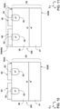
- Figure 1 shows a known JBS diode 1, of silicon carbide.
- the JBS diode 1 is generally formed by a plurality of elementary cells (just one is shown), which are equal to one another and are arranged in parallel in a same die; each elementary cell comprises a Schottky diode 2 and a pair of PN diodes 3, connected together in parallel.
- the JBS diode 1 is formed in a body 5 of silicon carbide (SiC), which is delimited by a first surface 5A and a second surface 5B opposite to one another along a first axis Z of a Cartesian reference system XYZ, and comprises a substrate 7 and a drift region 9 arranged on top of the substrate 7, for example epitaxially grown thereon.
- SiC silicon carbide
- the substrate 7 is of an N-type and forms the second surface 5B of the body 5.
- the drift region 9 is of an N-type, with a doping level lower than the doping level of the substrate 7, and forms the first surface 5A of the body 5.
- a cathode metallization region 10 of conductive material extends on the second surface 5B of the body 5 and forms a cathode K of the JBS diode 1.
- the JBS diode 1 further comprises a plurality of barrier regions 12, two of which are visible in Figure 1 , substantially housed in the drift region 9.
- the barrier regions 12 are arranged at a distance apart from each other along a second axis Y of the Cartesian reference system XYZ and are each formed by a respective implanted region 13 of a P-type, which extends from the first surface 5A of the body 5 into the drift region 9. Moreover, the barrier regions 12 extend along a third axis X of the Cartesian reference system XYZ.
- the barrier regions 12 each further comprise a respective ohmic contact region 14, of conductive material, for example nickel silicide, which extends on a respective implanted region 13, partially inside it, and, in the cross-section of Figure 1 , has an extension along the second axis Y smaller than or equal to the extension of the respective implanted region 13.
- conductive material for example nickel silicide
- the interfaces between the implanted regions 13 and the drift region 9 each form a PN diode 3.
- the JBS diode 1 further comprises an anode metallization region 18, of metal material such as titanium, nickel, or molybdenum, which extends on the first surface 5A of the body 5, forming an anode A of the JBS diode 1.
- anode metallization region 18, of metal material such as titanium, nickel, or molybdenum
- Schottky junctions i.e. semiconductor-metal junctions
- the Schottky junctions each have a respective barrier having, at equilibrium, a height ⁇ 0 , which determines a conduction threshold voltage of the respective Schottky diode 2.
- a bias voltage may be applied between the cathode K and the anode A of the JBS diode 1 so as to obtain a forward or reverse bias.
- a forward voltage is applied so as to lower the barrier height ⁇ 0 of the Schottky junctions, in order to switch on the Schottky diodes 2 and allow the flow of an operating current, for example of 10 A, between the anode A and the cathode K of the JBS diode 1.
- a low barrier height ⁇ 0 and thus a low conduction threshold voltage of the Schottky diodes 2, enables to reduce the value of the forward voltage that is necessary for the flow of the operating current and thus to achieve a low power consumption of the JBS diode 1.
- the JBS diode 1 in reverse bias (i.e. with the cathode K at a potential higher than the anode A), the JBS diode 1 must guarantee a value of the leakage current between the anode A and the cathode K as low as possible in the presence of high bias voltages, comprised, for example, between 600 V and 1300 V.
- Such high bias voltages generate high electrical fields in the Schottky junctions, causing an increase of the leakage current, for example because of the tunnel effect. Such an increase is particularly significant especially if the barrier height ⁇ 0 is small.
- each PN diode 3 causes formation of a respective depleted zone, having a low concentration of charge carriers, which extends from the interface between the respective implanted region 13 and the drift region 9, mainly inside the drift region 9.
- the depleted zone contributes to lower locally, in the proximity of a respective Schottky junction, the electrical field value generated by the high bias voltages.
- JBS diode 1 it is thus known to design the JBS diode 1 so as to provide a distance along the second axis Y between two adjacent implanted regions 13 that is as small as possible.
- a smaller distance between two adjacent implanted regions 13 enables in fact a greater lowering of the electrical field of the entire Schottky junction and consequently a lowering of the leakage current.
- a smaller distance between two adjacent implanted regions 13 entails a smaller area of the Schottky diode 2 available for the current flow in forward bias and thus a resistance increase of the JBS diode 1, with consequent worsening of the performance of the JBS diode 1.
- Document US 2008/203517 A1 discloses a device formed in a semiconductor body having a first semiconductor zone of the first conduction type, at least one first rectifying junction with respect to the first semiconductor zone and at least one second rectifying junction with respect to the first semiconductor zone, wherein the rectifying junctions each have a barrier height of different magnitude.
- Document US 2015/144966 A1 discloses a device formed in a semiconductor body of a first conduction type and a metal layer on the semiconductor body, wherein the metal layer forms with the semiconductor body a Schottky contact along a contact surface.
- a doping concentration of the first conduction type on the contact surface varies along a direction of the contact surface.
- Document US 6 562 706 B1 discloses a SiC dual metal trench diode comprising a drift layer, a Schottky contact metal located on top of the drift layer and a trench contact metal in the drift layer.
- the drift layer accommodates P-type regions at the bottom of the trench contact metal and N-type regions between the Schottky contact metal and the drift layer.
- the trench contact metal forms Schottky contacts that are contiguous to the P-type regions.
- the Schottky contact metal forms a Schottky contact with the N-type regions that is arranged at a distance from the P-type regions.
- the aim of the present invention is to overcome the drawbacks of the prior art.
- a wide band gap semiconductor electronic device comprising a JBS diode and a corresponding manufacturing method are provided, as defined in the annexed claims.
- JBS Joint Barrier Schottky
- Figures 2 and 2A show a JBS diode 50 which comprises, in this embodiment, a plurality of elementary cells 54 that are equal to one another, connected in parallel in a same die.
- each elementary cell 54 comprises one or more first-type Schottky diodes 51, one or more second-type Schottky diodes 52, and one or more PN diodes 53 arranged in parallel.
- each elementary cell 54 is formed by two first-type Schottky diodes 51 and by one second-type Schottky diode 52, arranged between two adjacent PN diodes 53.
- the JBS diode 50 is formed in a body 55 of silicon carbide (SiC), which is delimited by a first surface 55A and a second surface 55B opposite to one another along a first axis Z of a Cartesian reference system XYZ and comprises a substrate 57 and a drift region 59 arranged on top of the substrate 57, for example epitaxially grown thereon.
- SiC silicon carbide
- the substrate 57 is of an N-type, with doping level such as to have low resistivity, for example comprised between 2 m ⁇ cm and 30 m ⁇ cm, has a thickness comprised, for example, between 50 ⁇ m and 360 pm, in particular 180 pm, and forms the second surface 55B of the body 55.
- the drift region 59 is of an N-type, with a doping level lower than the doping level of the substrate 57, for example of the order of 10 16 at/cm 3 , has a thickness comprised between 5 ⁇ m and 15 pm, and forms the first surface 55A of the body 55.
- the thickness of the drift region 59 may be chosen at the design stage based on the specific application of the JBS diode 50, for example according to a maximum operating voltage to be applied to the JBS diode 50.
- a cathode metallization region 54 of conductive material extends on the second surface 55B of the body 55 and forms a cathode K of the JBS diode 50.
- the JBS diode 50 further comprises a plurality of implanted regions 62 housed in the drift region 59.
- the implanted regions 62 are of a P-type, have a doping level higher than the doping level of the drift region 59, each extend from the first surface 55A of the body 55 inside the drift region 59 for a depth, along the first axis Z, smaller than the depth of the drift region 59, and each have a width, along a second axis Y of the Cartesian reference system XYZ, comprised, for example, between 1 ⁇ m and 6 ⁇ m.
- the implanted regions 62 are arranged at a distance Sy apart from each other along the second axis Y, for example comprised between 2 ⁇ m and 5 ⁇ m.
- the implanted regions 62 may have the shape of strips, which extend longitudinally along a third axis X of the Cartesian reference system XYZ, or may have any other shape; for example, they may form regular or irregular geometrical figures, such as squares, rectangles, hexagons, or circles. Consequently, the implanted regions 62 illustrated in Figure 2 may be portions of a single region having a more complex shape, visible as separate regions in the illustrated cross-section.
- the interfaces between the implanted regions 62 and the drift region 59 form PN junctions, each forming a respective PN diode 53.
- the JBS diode 50 may further comprise a plurality of ohmic contact regions 63 of conductive material, each extending over a respective implanted region 62 and having a shape approximately corresponding to that of the implanted regions 62.
- Each ohmic-contact region 63 is in direct electrical contact with a respective implanted region 62 and extends, along the second axis Y, for a width smaller than or equal to the width of the respective implanted region 62.
- the ohmic-contact regions 63 are of nickel silicide, each extending partially within a respective implanted region 62, and having a width smaller than that of the respective implanted regions 62.
- the JBS diode 50 further comprises a plurality of anode metallization regions, one for each type of Schottky diode (as described in detail hereinafter), which extend on the first surface 55A of the body 55.
- the JBS diode 50 comprises first anode metallization regions 65 and a second anode metallization region 66.
- the first anode metallization regions 65 also have a shape approximately corresponding to that of the respective implanted regions 62, but have a greater width, as described in detail hereinafter; moreover, as explained above for the implanted regions 62, they may constitute portions of a first single anode metallization region 65 having a more complex shape. They are in any case electrically connected in parallel, so that they may be considered as a single region.
- the first anode metallization regions 65 are of a first metal material, for example molybdenum, and each comprise at least one first portion 65A ( Figure 2A ), which extends on, and is in direct electrical contact with, a respective first portion 59A of the drift region 59, in a position contiguous to the respective implanted region 62, on a side thereof.
- the first anode metallization regions 65 each further comprise a respective second portion 65B, which extends on, and is in direct electrical contact with, a respective implanted region 62 and a respective ohmic-contact region 63.
- the first portions 65A of the first anode metallization region 65 each have a width W 1 and are arranged at a distance W 2 from a first portion 65A of an adjacent first anode metallization region 65.
- the first portions 65A of the first anode metallization region 65 each form, with the respective first portion 59A of the drift region 59, a Schottky junction constituting a respective first-type Schottky diode 51 ( Figure 2 ).
- the junctions of the first-type Schottky diodes 51 each have a respective Schottky barrier having, at equilibrium, a height ⁇ 1 , for example of approximately 0.9 eV, which determines a first conduction threshold voltage of the respective first-type Schottky diode 51.
- the second anode metallization region 66 is of a second metal material, for example titanium or nickel, and extends on the first surface 55A of the body 55 and on the first anode metallization regions 65. Consequently ( Figure 2A ), portions 66A of the second metallization region 66 are in direct electrical contact (Schottky contact) with second portions 59B of the drift region 59 for a width equal to the distance W 2 between two first portions 65A of adjacent first anode metallization regions 65.
- the second portions 59B are arranged at a greater distance, with respect to the first portions 59A, from a respective same implanted region 62.
- the portions 66A of the second metallization region 66 thus form, with the second portions 59B of the drift region 59, Schottky junctions constituting respective second-type Schottky diodes 52 ( Figure 2 ).
- the junctions of the second-type Schottky diodes 52 each have a respective Schottky barrier having, at equilibrium, a height ⁇ 2 greater than the barrier height ⁇ 1 , for example of 1.2 eV, which determines a second conduction threshold voltage of the respective second-type Schottky diode 52 higher than the first conduction threshold voltage.
- the first and the second anode metallization regions 65, 66 further form an anode A of the JBS diode 50.
- a low voltage In use, in forward bias (voltage applied to the anode A higher than the voltage applied to the cathode K of the JBS diode 50), a low voltage enables the flow of a high operating current, for example of the value of 10 A, from the anode A to the cathode K of the JBS diode 50.
- the first-type Schottky diodes 51 enable a current flow in view of lower forward voltages compared to the second-type Schottky diodes 52 since the first conduction threshold voltage is lower than the second conduction threshold voltage.
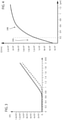
- the JBS diode 50 has a conduction threshold lower than the JBS diode 1 illustrated in Figure 1 , as represented in the simulation illustrated in Figure 3 performed by the Applicant, wherein the solid-line curve represents the plot of the current I as a function of the voltage V for the JBS diode 50 and the dashed line shows the same plot for the known JBS diode 1, with reference to an elementary cell.
- the JBS diode 50 it is possible to obtain the flow of a same current in view of a lower forward bias voltage applied between the anode A and the cathode K.
- the JBS diode 50 has a low power consumption in forward bias.
- high voltages between the anode A and the cathode K may be applied to the JBS diode 50.
- the interfaces between the implanted regions 62 and the drift region 59 each form a respective depleted region, having a low concentration of charge carriers, which locally lowers the electrical field generated by the high voltages, in particular in the proximity of the first surface 55A of the body 55.
- the depleted regions extend mainly in the drift region 59 since this has a doping level lower than that of the implanted regions 62.
- first portions 59A of the drift region 59 each extend at a smaller distance from a respective PN junction compared to the second portions 59B of the drift region 59.
- the first portions 59A are more affected by the influence of the respective depleted zone. Consequently, the first portions 59A are subject locally, in the proximity of the first surface 55A of the body 55, to an average electrical field lower than the average electrical field of the second portions 59B of the drift region 59.
- the electrical field in the drift region 59 in the proximity of the first surface 55A of the body 55, has a minimum value at the interface between the first portions 59A of the drift region 59 and the implanted regions 62, and increases moving away from the implanted regions 62 along the second axis Y, until it has a maximum value at the centre of the second portions 59B of the drift region 59, i.e., at a maximum distance from the implanted regions 62.
- the first-type Schottky diodes 51 extend in the first portions 59A of the drift region 59 and are thus subject to a low average electrical field.
- the first-type Schottky diodes 51 may thus guarantee a low leakage current in view of the high voltages applied in reverse bias.
- the second-type Schottky diodes 52 extend at the second portions 59B of the drift region 59 and are thus subject to a higher average electrical field.
- the second-type Schottky diodes52 have a barrier height ⁇ 2 greater than the barrier height ⁇ 1 and may thus guarantee low leakage currents even in the presence of a higher electrical field.
- the JBS diode 50 is able to obtain low leakage currents in reverse bias.
- the width W 1 and the distance W 2 may be tuned based on the characteristics of the JBS diode 50 required by a specific application. For instance, if it is preferable to obtain a low forward bias voltage, the width W 1 may be increased and the distance W 2 may be reduced. On the other hand, if it is preferable to obtain a low leakage current in reverse bias, the width W 1 may be reduced and the distance W 2 may be increased.
- the JBS diode 50 may be designed so that the distance Sy between two adjacent implanted regions 62 is large, for example up to the point where the depleted regions of two adjacent PN diodes 53 are in a condition of little overlap.
- the area of the first-type Schottky diodes 51 and of the second-type Schottky diodes 52 available for the current flow which depends, respectively, also on the width W 1 and the distance W 2 , is bigger than for a smaller distance S Y . Consequently, as a whole, the JBS diode 50 may have a bigger area available for the passage of current and thus a lower resistance in forward bias.
- the JBS diode 50 is able to provide both a low power consumption in forward bias and a low leakage current in reverse bias.
- Figure 5 shows a JBS diode 100 according to another embodiment.
- the JBS diode 100 has a structure similar to the JBS diode 50, and thus the elements in common are designated by the same reference numbers.
- the JBS diode 100 comprises first-type Schottky diodes 101 and second-type Schottky diodes 102, as well as the PN diodes 53, and is formed in the body 55.
- the body 55 also here comprises the substrate 57, the drift region 59, the implanted regions 62, and the ohmic-contact regions 63.
- the cathode metallization region 54 extends on the second surface 55B of the body 55.
- the JBS diode 100 further comprises a plurality of implanted anode regions 105, of an N-type, which extend from the first surface 55A of the body 55 into the drift region 59, alongside each implanted region 62.
- the implanted anode regions 105 have a doping level higher than the doping level of the drift region 59; for example, they have a concentration of dopant atoms higher than 1-10 17 at/cm 3 and a small depth, for example comprised between 10 nm and 100 nm.
- the implanted anode regions 105 each extend in the drift region 59, contiguous to a respective implanted region 62, each have a width Wi, and are arranged at the distance W 2 from a respective adjacent implanted anode region 105, as explained previously with reference to the JBS diode 50 for the first portions 65A of the first anode metallization regions 65.
- the implanted anode regions 105 constitute surface portions of the drift region 59 similar to the first portions 59A of the JBS diode 50 and have a higher doping level than first portions 59A.
- An anode metallization region 115 for example of molybdenum, titanium, or nickel extends on the first surface 55A of the body 55 and on the ohmic-contact regions 63.
- First portions 115A of the anode metallization region 115 in direct electrical contact (Schottky contact) with the implanted anode regions 105 each form a respective first-type Schottky diode 101; each first-type Schottky diode 101 has, at equilibrium, a Schottky barrier having a height ⁇ 1 .
- the difference of barrier height between the Schottky diodes 101 and the second-type Schottky diodes 102 depends upon the difference between the doping level of the implanted anode regions 105 and the doping level of the drift region 59. This difference may be regulated, at the design stage, according to the specific applications.
- the Schottky junctions of the first-type Schottky diodes 101 have a smaller barrier height and are subject to lower electrical fields as compared to the Schottky junctions of the second-type Schottky diodes 102.
- the JBS diode 100 has a low power consumption, a low leakage current, and a high adaptability to different operating conditions.
- FIG. 6 shows a further embodiment of the present JBS diode, herein referred to as JBS diode 200.
- the JBS diode 200 has a general structure similar to the JBS diodes 50, 100, so that elements in common are designated by the same reference numbers.
- the JBS diode 200 comprises first-type Schottky diodes 201 and second-type Schottky diodes 202, as well as the PN diodes 53, and is formed in the body 55 comprising the substrate 57.
- the substrate also here comprises the drift region 59, the implanted regions 62, the ohmic-contact regions 63, and the implanted anode regions 105.
- the cathode metallization region 54 extends on the second surface 55B of the body 55.
- the JBS diode 200 comprises first anode metallization regions 215 and a second anode metallization region 216, which extend on the first surface 55A of the body 55.
- the first anode metallization regions 215 have a shape similar to that of the first anode metallization regions 65 described with reference to the JBS diode 50 of Figure 2 and are also of the first metal material, for example molybdenum.
- first anode metallization regions 215 each comprise a plurality of portions that include at least one first portion 215A having a width Wi, and are arranged on top of, and in direct electrical contact (Schottky contact) with, a respective implanted anode region 105.
- each first anode metallization region 215 also comprises a second portion 215B, which extends on a respective implanted region 62 and a respective ohmic-contact region 63 and is in direct electrical contact therewith.
- the first portions 215A of the first anode metallization regions 215 in Schottky contact with the respective implanted anode regions 105 form the first-type Schottky diodes 201, which each have a Schottky junction having, at equilibrium, a Schottky barrier of height ⁇ 1 .
- the second anode metallization region 216 is of the second metal material, for example titanium or nickel, and extends on the first surface 55A of the body 55 and on the first anode metallization regions 215.
- portions 216A of the second anode metallization region 216 are in direct electrical contact (Schottky contact) with the second portions 59B of the drift region 59 arranged between two adjacent implanted anode regions 105, which thus have a width equal to the distance W 2 .
- the portions 216A of the second anode metallization region 216 form, with the second portions 59B of the drift region 59, the second-type Schottky diodes 202, which each have a Schottky junction having, at equilibrium, a barrier of a height ⁇ 2 greater than the barrier having a height ⁇ 1 of the first-type Schottky diodes 201.
- the barrier height of the first-type Schottky diodes 201 and of the second-type Schottky diodes 202 may be regulated both by modifying the difference between the doping level of the implanted anode regions 105 and of the drift region 59 and by modifying the difference of barrier height induced by the first metal material and the second metal material, which form, respectively, the first anode metallization regions 215 and the second anode metallization region 216.
- the JBS diode 200 thus has similar advantages to the ones explained previously as regards the JBS diodes 50, 100, and has a greater adaptability to different operating conditions, which may be regulated at the design stage.
- FIG. 7 shows a further embodiment of the present JBS diode, herein referred to as JBS diode 250.
- the JBS diode 250 has a structure similar to that of the JBS diode 200, and thus elements in common are designated by the same reference numbers.
- the JBS diode 250 comprises first-type Schottky diodes 251, second-type Schottky diodes 252, and third-type Schottky diodes 253, arranged in parallel with the PN diodes 53.
- portions 265A of first anode metallization regions 265 each extend on a first portion 105A of a respective implanted anode region 105 contiguous to a respective implanted region 62, for a width smaller than the width W 1 of the implanted anode regions 105.
- a second anode metallization region 266 (which is similar to the second anode metallization region 216 of the JBS diode 200), extends on the first surface 55A of the body 55.
- first portions 266A of the second anode metallization region 266 are in direct electrical contact (Schottky contact) with the second portions 59B of the drift region 59, and second portions 266B of the second anode metallization region 266 are in direct electrical contact (Schottky contact) with second portions 105B of the implanted anode regions 105 contiguous to the first portions 105A.
- the second portions 105B of the implanted anode regions 105 are thus each arranged between a respective first portion 105A of the implanted anode regions 105 and a respective second portion 59B of the drift region 59.
- the second portions 105B of the implanted anode regions 105 each are at a greater distance than a respective first portion 105A from a same respective implanted region 62, and at a smaller distance than a respective second portion 59B from the same respective implanted region 62.
- first portions 265A of the first anode metallization regions 265 in direct electrical contact with the first portions 105A of the implanted anode regions 105 form Schottky junctions that have a barrier, at equilibrium, of a height ⁇ 1 and form the first-type Schottky diodes 251.
- the first portions 266A of the second anode metallization region 266 in direct electrical contact with the second portions 59B of the drift region 59 form Schottky junctions that have a barrier, at equilibrium, of a height ⁇ 2 greater than the height ⁇ 1 , and that form the second-type Schottky diodes 252.
- the second portions 266B of the second anode metallization region 266 in direct electrical contact with the second portions 105B of the implanted anode regions 105 form Schottky junctions that have a barrier, at equilibrium, of a height O 3 greater than the height ⁇ 1 and smaller than the height ⁇ 2 , and that form the third-type Schottky diodes 253.
- the third-type Schottky diodes 253 thus have a conduction threshold voltage lower than that of the second-type Schottky diodes 252.
- the JBS diode 250 has a low conduction threshold and a consequent low power consumption.
- the third-type Schottky diodes 253 are arranged at the second portions 105B of the implanted anode regions 105, which, being arranged at a distance from an adjacent implanted region 62 that is smaller than the distance of the second portions 59B from the same adjacent implanted region 62, are subject, in reverse bias, to a lower average electrical field than are the second portions 59B of the drift region 59.
- the first-type Schottky diodes 251, the second-type Schottky diodes 252, and the third-type Schottky diodes 253 may also guarantee low leakage currents for the JBS diode 250.
- the JBS diode 50 may be manufactured from a wafer 300 of silicon carbide (SiC), illustrated in cross-section in Figure 8 , having a first surface 300A and a second surface 300B, and already subjected to first known processing steps.
- SiC silicon carbide
- the wafer 300 has already been processed so as to form the body 55 (the first and the second surfaces 55A, 55B of which correspond, respectively, to the first surface 300A and to the second surface 300B of the wafer 300) comprising the substrate 57, the drift region 59, the implanted regions 62, and the ohmic-contact regions 63.
- a first metallization layer 305 of the first metal material for example molybdenum, is deposited on the first surface 300A of the wafer 300 and patterned ( Figure 10 ), via known lithographic steps so as to form the first anode metallization regions 65.
- the second metal material for example titanium or nickel
- Known processing steps follow, such as thinning the substrate 57, forming the cathode metallization region on the second surface 300B of the wafer 300, dicing the wafer 300, and packaging, to obtain the JBS diode 50.
- the JBS diode 100 may be manufactured from a wafer 400 of silicon carbide illustrated in Figure 12 .
- the wafer 400 is similar to the wafer 300 illustrated in Figure 8 ; consequently, similar elements are designated by the same reference numbers.
- the wafer 400 having a first surface 400A and a second surface 400B, has already been processed so as to form the substrate 57, the drift region 59, and the implanted regions 62.
- a hard mask 401 comprising a plurality of windows 402, is provided on the first surface 400A of the wafer 400.
- the windows 402 are arranged above the implanted regions 62 and above portions of the drift region contiguous to the respective implanted regions 62, where the implanted anode regions 105 are intended to be formed.
- the windows 402 are used for implanting ions, as schematically represented by the arrows 405, and forming doped regions 410, here of an N-type, which are intended to form the implanted anode regions 105.
- the ions may be implanted with a dose comprised, for example, between 10 11 and 10 13 at/cm 2 , in particular 10 12 at/cm 2 .
- This dose is in fact sufficient to increase the doping level of the respective portions of the drift region 59, without jeopardizing the doping of the implanted regions 62.
- the hard mask 401 may comprise portions (not illustrated) that extend also on the implanted regions 62 so that the windows 402 are arranged only above the portions of the drift region 59 where the implanted anode regions 105 are intended to be formed.
- the hard mask 401 is then removed, and the wafer 400 is subjected to annealing for activation of the doped regions 410, for example at a temperature higher than 1500°C, so as to form the implanted anode regions 105 ( Figure 14 ).
- the ohmic-contact regions 63 are formed in a known way, and a first metallization layer 406, of the second metal material, for example titanium or nickel, is deposited on the first surface 400A of the wafer 400 so as to form the second anode metallization region 115.
- a first metallization layer 406, of the second metal material for example titanium or nickel
- Known processing steps follow, such as thinning the substrate 57, forming the cathode metallization region on the second surface 400B of the wafer 400, dicing the wafer 400, and packaging, to obtain the JBS diode 100.
- JBS diodes 200, 250 may be obtained, from the wafer 400 of Figure 12 , through steps similar to the ones already described with reference to Figures 9-14 regarding the JBS diodes 50, 100, and thus are not illustrated any further.
- the conductivity types, P and N may be reversed, and what described above may also be applied to an MPS ("Merged PiN Schottky”) diode.
- MPS Merged PiN Schottky
Landscapes
- Electrodes Of Semiconductors (AREA)
Abstract
Description
- The present invention relates to a wide band gap semiconductor electronic device, comprising a JBS (Junction-Barrier Schottky) diode having improved electrical characteristics and to the corresponding manufacturing method. In particular, reference will be made hereinafter to a vertical-conduction electronic power device.
- As is known, semiconductor materials that have a wide band gap, for example greater than 1.1 eV, low ON-state resistance, high thermal conductivity, high operating frequency, and high rate of saturation of the charge carriers, such as silicon carbide (SiC) and gallium nitride (GaN), allows to obtain electronic devices, for example diodes and transistors, that have better performances than silicon electronic devices, in particular for power applications, for example operating at voltages comprised between 600 V and 1300 V or in specific operating conditions, such as high temperature.
- In particular, it is known to obtain the above electronic devices from a wafer of silicon carbide in one of its polytypes, for example 3C-SiC, 4H-SiC and 6H-SiC, which are distinguished by the characteristics listed above.
- For instance,
Figure 1 shows a knownJBS diode 1, of silicon carbide. TheJBS diode 1 is generally formed by a plurality of elementary cells (just one is shown), which are equal to one another and are arranged in parallel in a same die; each elementary cell comprises a Schottkydiode 2 and a pair ofPN diodes 3, connected together in parallel. - The
JBS diode 1 is formed in abody 5 of silicon carbide (SiC), which is delimited by afirst surface 5A and asecond surface 5B opposite to one another along a first axis Z of a Cartesian reference system XYZ, and comprises asubstrate 7 and adrift region 9 arranged on top of thesubstrate 7, for example epitaxially grown thereon. - The
substrate 7 is of an N-type and forms thesecond surface 5B of thebody 5. - The
drift region 9 is of an N-type, with a doping level lower than the doping level of thesubstrate 7, and forms thefirst surface 5A of thebody 5. - A
cathode metallization region 10 of conductive material, for example nickel or nickel silicide, extends on thesecond surface 5B of thebody 5 and forms a cathode K of theJBS diode 1. - The
JBS diode 1 further comprises a plurality ofbarrier regions 12, two of which are visible inFigure 1 , substantially housed in thedrift region 9. - The
barrier regions 12 are arranged at a distance apart from each other along a second axis Y of the Cartesian reference system XYZ and are each formed by a respective implantedregion 13 of a P-type, which extends from thefirst surface 5A of thebody 5 into thedrift region 9. Moreover, thebarrier regions 12 extend along a third axis X of the Cartesian reference system XYZ. - The
barrier regions 12 each further comprise a respectiveohmic contact region 14, of conductive material, for example nickel silicide, which extends on a respective implantedregion 13, partially inside it, and, in the cross-section ofFigure 1 , has an extension along the second axis Y smaller than or equal to the extension of the respective implantedregion 13. - The interfaces between the implanted
regions 13 and thedrift region 9 each form aPN diode 3. - The
JBS diode 1 further comprises ananode metallization region 18, of metal material such as titanium, nickel, or molybdenum, which extends on thefirst surface 5A of thebody 5, forming an anode A of theJBS diode 1. - Portions of the
anode metallization region 18 in direct electrical contact with thedrift region 9, alongside the implantedregions 13, form Schottky junctions (i.e. semiconductor-metal junctions), each constituting a respective Schottkydiode 2. - The Schottky junctions each have a respective barrier having, at equilibrium, a height Φ0, which determines a conduction threshold voltage of the
respective Schottky diode 2. - In use, a bias voltage may be applied between the cathode K and the anode A of the
JBS diode 1 so as to obtain a forward or reverse bias. - In detail, in forward bias (anode A at a potential higher than the cathode K), a forward voltage is applied so as to lower the barrier height Φ0 of the Schottky junctions, in order to switch on the Schottky
diodes 2 and allow the flow of an operating current, for example of 10 A, between the anode A and the cathode K of theJBS diode 1. - A low barrier height Φ0, and thus a low conduction threshold voltage of the
Schottky diodes 2, enables to reduce the value of the forward voltage that is necessary for the flow of the operating current and thus to achieve a low power consumption of theJBS diode 1. - On the other hand, in reverse bias (i.e. with the cathode K at a potential higher than the anode A), the
JBS diode 1 must guarantee a value of the leakage current between the anode A and the cathode K as low as possible in the presence of high bias voltages, comprised, for example, between 600 V and 1300 V. - Such high bias voltages generate high electrical fields in the Schottky junctions, causing an increase of the leakage current, for example because of the tunnel effect. Such an increase is particularly significant especially if the barrier height Φ0 is small.
- Consequently, a small barrier height Φ0 causes a high leakage current and thus problems of operation of the
JBS diode 1. - Moreover, in reverse bias, each
PN diode 3 causes formation of a respective depleted zone, having a low concentration of charge carriers, which extends from the interface between the respective implantedregion 13 and thedrift region 9, mainly inside thedrift region 9. - The depleted zone contributes to lower locally, in the proximity of a respective Schottky junction, the electrical field value generated by the high bias voltages.
- It is thus known to design the
JBS diode 1 so as to provide a distance along the second axis Y between two adjacent implantedregions 13 that is as small as possible. A smaller distance between two adjacent implantedregions 13 enables in fact a greater lowering of the electrical field of the entire Schottky junction and consequently a lowering of the leakage current. - However, a smaller distance between two adjacent implanted
regions 13 entails a smaller area of the Schottkydiode 2 available for the current flow in forward bias and thus a resistance increase of theJBS diode 1, with consequent worsening of the performance of theJBS diode 1. - Document
US 2008/203517 A1 discloses a device formed in a semiconductor body having a first semiconductor zone of the first conduction type, at least one first rectifying junction with respect to the first semiconductor zone and at least one second rectifying junction with respect to the first semiconductor zone, wherein the rectifying junctions each have a barrier height of different magnitude. - Document
US 2015/144966 A1 discloses a device formed in a semiconductor body of a first conduction type and a metal layer on the semiconductor body, wherein the metal layer forms with the semiconductor body a Schottky contact along a contact surface. A doping concentration of the first conduction type on the contact surface varies along a direction of the contact surface. - Document
US 6 562 706 B1 discloses a SiC dual metal trench diode comprising a drift layer, a Schottky contact metal located on top of the drift layer and a trench contact metal in the drift layer. The drift layer accommodates P-type regions at the bottom of the trench contact metal and N-type regions between the Schottky contact metal and the drift layer. The trench contact metal forms Schottky contacts that are contiguous to the P-type regions. The Schottky contact metal forms a Schottky contact with the N-type regions that is arranged at a distance from the P-type regions. - Document
JP 2000 196107 A - The aim of the present invention is to overcome the drawbacks of the prior art.
- According to the present invention, a wide band gap semiconductor electronic device comprising a JBS diode and a corresponding manufacturing method are provided, as defined in the annexed claims.
- For a better understanding of the present invention, embodiments thereof are now described, purely by way of nonlimiting example, with reference to the attached drawings, wherein:
-
Figure 1 is a cross-section of a known wide band gap electronic semiconductor power device; -
Figure 2 is a cross-section of an embodiment of the present wide band gap electronic semiconductor power device wherein electrical equivalents are highlighted; -
Figure 2A shows an enlarged detail ofFigure 2 , wherein geometrical parameters of the present electronic device are highlighted; -
Figure 3 shows a simulation of the forward bias current-voltage curve of an elementary cell of the electronic device ofFigure 2 compared with an elementary cell of the known electronic device ofFigure 1 ; -
Figure 4 shows a graph of the behaviour of the electrical field alongsection line 80 ofFigure 2A ; -
Figure 5 shows a cross-section of the present wide band gap electronic semiconductor power device according to another embodiment; -
Figure 6 shows a cross-section of the present wide band gap electronic semiconductor power device according to a further embodiment; -
Figure 7 shows a cross-section of the present wide band gap electronic semiconductor power device according to a further embodiment; -
Figures 8-11 show cross-sections of the electronic power device ofFigure 2 in successive manufacturing steps; and -
Figures 12-14 show cross-sections of the electronic device ofFigure 5 in successive manufacturing steps. - Described hereinafter is a wide band gap semiconductor JBS (Junction Barrier Schottky) diode, in particular of silicon carbide, which is incorporated in a vertical-conduction electronic power device and comprises a plurality of Schottky diodes of different types, wherein each type of Schottky diode has a Schottky junction that has, at equilibrium, a different barrier height.
- In detail,
Figures 2 and2A show aJBS diode 50 which comprises, in this embodiment, a plurality ofelementary cells 54 that are equal to one another, connected in parallel in a same die. - As shown in particular in
Figure 2 , eachelementary cell 54 comprises one or more first-type Schottkydiodes 51, one or more second-type Schottkydiodes 52, and one ormore PN diodes 53 arranged in parallel. In particular, in this embodiment, eachelementary cell 54 is formed by two first-type Schottkydiodes 51 and by one second-type Schottkydiode 52, arranged between twoadjacent PN diodes 53. - The JBS
diode 50 is formed in abody 55 of silicon carbide (SiC), which is delimited by afirst surface 55A and asecond surface 55B opposite to one another along a first axis Z of a Cartesian reference system XYZ and comprises asubstrate 57 and adrift region 59 arranged on top of thesubstrate 57, for example epitaxially grown thereon. - The
substrate 57 is of an N-type, with doping level such as to have low resistivity, for example comprised between 2 mΩ·cm and 30 mΩ·cm, has a thickness comprised, for example, between 50 µm and 360 pm, in particular 180 pm, and forms thesecond surface 55B of thebody 55. - The
drift region 59 is of an N-type, with a doping level lower than the doping level of thesubstrate 57, for example of the order of 1016 at/cm3, has a thickness comprised between 5 µm and 15 pm, and forms thefirst surface 55A of thebody 55. - The thickness of the
drift region 59 may be chosen at the design stage based on the specific application of theJBS diode 50, for example according to a maximum operating voltage to be applied to theJBS diode 50. - A
cathode metallization region 54 of conductive material, for example nickel or nickel silicide, extends on thesecond surface 55B of thebody 55 and forms a cathode K of theJBS diode 50. - The JBS
diode 50 further comprises a plurality of implantedregions 62 housed in thedrift region 59. - The implanted
regions 62 are of a P-type, have a doping level higher than the doping level of thedrift region 59, each extend from thefirst surface 55A of thebody 55 inside thedrift region 59 for a depth, along the first axis Z, smaller than the depth of thedrift region 59, and each have a width, along a second axis Y of the Cartesian reference system XYZ, comprised, for example, between 1 µm and 6 µm. - Moreover, the implanted
regions 62 are arranged at a distance Sy apart from each other along the second axis Y, for example comprised between 2 µm and 5 µm. - In top view (not illustrated herein), the implanted
regions 62 may have the shape of strips, which extend longitudinally along a third axis X of the Cartesian reference system XYZ, or may have any other shape; for example, they may form regular or irregular geometrical figures, such as squares, rectangles, hexagons, or circles. Consequently, the implantedregions 62 illustrated inFigure 2 may be portions of a single region having a more complex shape, visible as separate regions in the illustrated cross-section. - The interfaces between the implanted
regions 62 and thedrift region 59 form PN junctions, each forming arespective PN diode 53. - The
JBS diode 50 may further comprise a plurality ofohmic contact regions 63 of conductive material, each extending over a respective implantedregion 62 and having a shape approximately corresponding to that of the implantedregions 62. Each ohmic-contact region 63 is in direct electrical contact with a respective implantedregion 62 and extends, along the second axis Y, for a width smaller than or equal to the width of the respective implantedregion 62. - In detail, in this embodiment, the ohmic-
contact regions 63 are of nickel silicide, each extending partially within a respective implantedregion 62, and having a width smaller than that of the respective implantedregions 62. - The
JBS diode 50 further comprises a plurality of anode metallization regions, one for each type of Schottky diode (as described in detail hereinafter), which extend on thefirst surface 55A of thebody 55. In this embodiment, theJBS diode 50 comprises firstanode metallization regions 65 and a secondanode metallization region 66. - The first
anode metallization regions 65 also have a shape approximately corresponding to that of the respective implantedregions 62, but have a greater width, as described in detail hereinafter; moreover, as explained above for the implantedregions 62, they may constitute portions of a first singleanode metallization region 65 having a more complex shape. They are in any case electrically connected in parallel, so that they may be considered as a single region. - The first
anode metallization regions 65 are of a first metal material, for example molybdenum, and each comprise at least onefirst portion 65A (Figure 2A ), which extends on, and is in direct electrical contact with, a respectivefirst portion 59A of thedrift region 59, in a position contiguous to the respective implantedregion 62, on a side thereof. In this embodiment, the firstanode metallization regions 65 each further comprise a respectivesecond portion 65B, which extends on, and is in direct electrical contact with, a respective implantedregion 62 and a respective ohmic-contact region 63. - The
first portions 65A of the firstanode metallization region 65 each have a width W1 and are arranged at a distance W2 from afirst portion 65A of an adjacent firstanode metallization region 65. - The
first portions 65A of the firstanode metallization region 65 each form, with the respectivefirst portion 59A of thedrift region 59, a Schottky junction constituting a respective first-type Schottky diode 51 (Figure 2 ). The junctions of the first-type Schottky diodes 51 each have a respective Schottky barrier having, at equilibrium, a height Φ1, for example of approximately 0.9 eV, which determines a first conduction threshold voltage of the respective first-type Schottky diode 51. - The second
anode metallization region 66 is of a second metal material, for example titanium or nickel, and extends on thefirst surface 55A of thebody 55 and on the firstanode metallization regions 65. Consequently (Figure 2A ),portions 66A of thesecond metallization region 66 are in direct electrical contact (Schottky contact) withsecond portions 59B of thedrift region 59 for a width equal to the distance W2 between twofirst portions 65A of adjacent firstanode metallization regions 65. - In other words, the
second portions 59B are arranged at a greater distance, with respect to thefirst portions 59A, from a respective same implantedregion 62. - The
portions 66A of thesecond metallization region 66 thus form, with thesecond portions 59B of thedrift region 59, Schottky junctions constituting respective second-type Schottky diodes 52 (Figure 2 ). The junctions of the second-type Schottky diodes 52 each have a respective Schottky barrier having, at equilibrium, a height Φ2 greater than the barrier height Φ1, for example of 1.2 eV, which determines a second conduction threshold voltage of the respective second-type Schottky diode 52 higher than the first conduction threshold voltage. - The first and the second
anode metallization regions JBS diode 50. - In use, in forward bias (voltage applied to the anode A higher than the voltage applied to the cathode K of the JBS diode 50), a low voltage enables the flow of a high operating current, for example of the value of 10 A, from the anode A to the cathode K of the
JBS diode 50. - In fact, the first-
type Schottky diodes 51 enable a current flow in view of lower forward voltages compared to the second-type Schottky diodes 52 since the first conduction threshold voltage is lower than the second conduction threshold voltage. - Consequently, as a whole, the
JBS diode 50 has a conduction threshold lower than theJBS diode 1 illustrated inFigure 1 , as represented in the simulation illustrated inFigure 3 performed by the Applicant, wherein the solid-line curve represents the plot of the current I as a function of the voltage V for theJBS diode 50 and the dashed line shows the same plot for the knownJBS diode 1, with reference to an elementary cell. As may be noted, with theJBS diode 50 it is possible to obtain the flow of a same current in view of a lower forward bias voltage applied between the anode A and the cathode K. - Consequently, the
JBS diode 50 has a low power consumption in forward bias. - In reverse bias, high voltages between the anode A and the cathode K, for example comprised between 600 V and 1300 V, may be applied to the
JBS diode 50. - In reverse bias, the interfaces between the implanted
regions 62 and thedrift region 59 each form a respective depleted region, having a low concentration of charge carriers, which locally lowers the electrical field generated by the high voltages, in particular in the proximity of thefirst surface 55A of thebody 55. - In fact, in this embodiment, the depleted regions extend mainly in the
drift region 59 since this has a doping level lower than that of the implantedregions 62. - In particular, the
first portions 59A of thedrift region 59 each extend at a smaller distance from a respective PN junction compared to thesecond portions 59B of thedrift region 59. - Thus, the
first portions 59A are more affected by the influence of the respective depleted zone. Consequently, thefirst portions 59A are subject locally, in the proximity of thefirst surface 55A of thebody 55, to an average electrical field lower than the average electrical field of thesecond portions 59B of thedrift region 59. - In other words, the electrical field in the
drift region 59, in the proximity of thefirst surface 55A of thebody 55, has a minimum value at the interface between thefirst portions 59A of thedrift region 59 and the implantedregions 62, and increases moving away from the implantedregions 62 along the second axis Y, until it has a maximum value at the centre of thesecond portions 59B of thedrift region 59, i.e., at a maximum distance from the implantedregions 62. - The above electrical behaviour is illustrated in the simulation of
Figure 4 performed by the Applicant, which shows the behaviour of the electrical field E along theline 80 ofFigure 2A , which extends in a direction parallel to thefirst surface 55A from the interface between an implantedregion 62 and afirst portion 59A of thedrift region 59 to a central point of thesecond portion 59B of thedrift region 59. - The first-
type Schottky diodes 51 extend in thefirst portions 59A of thedrift region 59 and are thus subject to a low average electrical field. - The first-
type Schottky diodes 51 may thus guarantee a low leakage current in view of the high voltages applied in reverse bias. - The second-
type Schottky diodes 52 extend at thesecond portions 59B of thedrift region 59 and are thus subject to a higher average electrical field. - However, the second-type Schottky diodes52 have a barrier height Φ2 greater than the barrier height Φ1 and may thus guarantee low leakage currents even in the presence of a higher electrical field.
- It follows that, as a whole, the
JBS diode 50 is able to obtain low leakage currents in reverse bias. - At the design stage, by maintaining the distance Sy between two adjacent implanted
regions 62 constant, the width W1 and the distance W2 may be tuned based on the characteristics of theJBS diode 50 required by a specific application. For instance, if it is preferable to obtain a low forward bias voltage, the width W1 may be increased and the distance W2 may be reduced. On the other hand, if it is preferable to obtain a low leakage current in reverse bias, the width W1 may be reduced and the distance W2 may be increased. - In addition, the
JBS diode 50 may be designed so that the distance Sy between two adjacent implantedregions 62 is large, for example up to the point where the depleted regions of twoadjacent PN diodes 53 are in a condition of little overlap. - The fact that two adjacent
depleted regions 62 are in a condition of little overlap causes a higher average electrical field in thesecond portions 59B of thedrift region 59, compared to a case wherein the distance SY is smaller. However, the greater barrier height of the second-type Schottky diodes 52 enables to compensate such greater average electrical field and thus to guarantee a low leakage current. Furthermore, a greater distance Sy enables theJBS diode 50 to have a lower resistance to the current flow between the anode and the cathode, and thus a low power consumption, in forward bias. - When the distance Sy is large, in fact, the area of the first-
type Schottky diodes 51 and of the second-type Schottky diodes 52 available for the current flow, which depends, respectively, also on the width W1 and the distance W2, is bigger than for a smaller distance SY. Consequently, as a whole, theJBS diode 50 may have a bigger area available for the passage of current and thus a lower resistance in forward bias. - In other words, the
JBS diode 50 is able to provide both a low power consumption in forward bias and a low leakage current in reverse bias. -
Figure 5 shows aJBS diode 100 according to another embodiment. - The
JBS diode 100 has a structure similar to theJBS diode 50, and thus the elements in common are designated by the same reference numbers. - In detail, the
JBS diode 100 comprises first-type Schottky diodes 101 and second-type Schottky diodes 102, as well as thePN diodes 53, and is formed in thebody 55. Thebody 55 also here comprises thesubstrate 57, thedrift region 59, the implantedregions 62, and the ohmic-contact regions 63. In addition, thecathode metallization region 54 extends on thesecond surface 55B of thebody 55. - The
JBS diode 100 further comprises a plurality of implantedanode regions 105, of an N-type, which extend from thefirst surface 55A of thebody 55 into thedrift region 59, alongside each implantedregion 62. The implantedanode regions 105 have a doping level higher than the doping level of thedrift region 59; for example, they have a concentration of dopant atoms higher than 1-1017 at/cm3 and a small depth, for example comprised between 10 nm and 100 nm. - In detail, the implanted
anode regions 105 each extend in thedrift region 59, contiguous to a respective implantedregion 62, each have a width Wi, and are arranged at the distance W2 from a respective adjacent implantedanode region 105, as explained previously with reference to theJBS diode 50 for thefirst portions 65A of the firstanode metallization regions 65. - Thus, the implanted
anode regions 105 constitute surface portions of thedrift region 59 similar to thefirst portions 59A of theJBS diode 50 and have a higher doping level thanfirst portions 59A. - An
anode metallization region 115, for example of molybdenum, titanium, or nickel extends on thefirst surface 55A of thebody 55 and on the ohmic-contact regions 63. -
First portions 115A of theanode metallization region 115 in direct electrical contact (Schottky contact) with the implantedanode regions 105 each form a respective first-type Schottky diode 101; each first-type Schottky diode 101 has, at equilibrium, a Schottky barrier having a height Φ1. -
Second portions 115B of theanode metallization region 115 in direct electrical contact with thesecond portions 59B of thedrift region 59, having a width equal to the distance W2 between two adjacent implantedanode regions 105, each form a respective second-type Schottky diode 102; each second-type Schottky diode 102 has, at equilibrium, a Schottky barrier having a height Φ2 greater than that of the first-type Schottky diodes 101. - In this embodiment, the difference of barrier height between the
Schottky diodes 101 and the second-type Schottky diodes 102 depends upon the difference between the doping level of the implantedanode regions 105 and the doping level of thedrift region 59. This difference may be regulated, at the design stage, according to the specific applications. - As explained previously with reference to the
JBS diode 50, the Schottky junctions of the first-type Schottky diodes 101 have a smaller barrier height and are subject to lower electrical fields as compared to the Schottky junctions of the second-type Schottky diodes 102. - Thus, as a whole, the
JBS diode 100 has a low power consumption, a low leakage current, and a high adaptability to different operating conditions. -
Figure 6 shows a further embodiment of the present JBS diode, herein referred to asJBS diode 200. - The
JBS diode 200 has a general structure similar to theJBS diodes - In detail, the
JBS diode 200 comprises first-type Schottky diodes 201 and second-type Schottky diodes 202, as well as thePN diodes 53, and is formed in thebody 55 comprising thesubstrate 57. The substrate also here comprises thedrift region 59, the implantedregions 62, the ohmic-contact regions 63, and the implantedanode regions 105. Furthermore, thecathode metallization region 54 extends on thesecond surface 55B of thebody 55. - Moreover, the
JBS diode 200 comprises firstanode metallization regions 215 and a secondanode metallization region 216, which extend on thefirst surface 55A of thebody 55. - The first
anode metallization regions 215 have a shape similar to that of the firstanode metallization regions 65 described with reference to theJBS diode 50 ofFigure 2 and are also of the first metal material, for example molybdenum. - In particular, the first
anode metallization regions 215 each comprise a plurality of portions that include at least onefirst portion 215A having a width Wi, and are arranged on top of, and in direct electrical contact (Schottky contact) with, a respective implantedanode region 105. In this embodiment, each firstanode metallization region 215 also comprises asecond portion 215B, which extends on a respective implantedregion 62 and a respective ohmic-contact region 63 and is in direct electrical contact therewith. - The
first portions 215A of the firstanode metallization regions 215 in Schottky contact with the respective implantedanode regions 105 form the first-type Schottky diodes 201, which each have a Schottky junction having, at equilibrium, a Schottky barrier of height Φ1. - The second
anode metallization region 216 is of the second metal material, for example titanium or nickel, and extends on thefirst surface 55A of thebody 55 and on the firstanode metallization regions 215. - Consequently,
portions 216A of the secondanode metallization region 216 are in direct electrical contact (Schottky contact) with thesecond portions 59B of thedrift region 59 arranged between two adjacent implantedanode regions 105, which thus have a width equal to the distance W2. Theportions 216A of the secondanode metallization region 216 form, with thesecond portions 59B of thedrift region 59, the second-type Schottky diodes 202, which each have a Schottky junction having, at equilibrium, a barrier of a height Φ2 greater than the barrier having a height Φ1 of the first-type Schottky diodes 201. - In this embodiment, the barrier height of the first-
type Schottky diodes 201 and of the second-type Schottky diodes 202 may be regulated both by modifying the difference between the doping level of the implantedanode regions 105 and of thedrift region 59 and by modifying the difference of barrier height induced by the first metal material and the second metal material, which form, respectively, the firstanode metallization regions 215 and the secondanode metallization region 216. - The
JBS diode 200 thus has similar advantages to the ones explained previously as regards theJBS diodes -
Figure 7 shows a further embodiment of the present JBS diode, herein referred to asJBS diode 250. TheJBS diode 250 has a structure similar to that of theJBS diode 200, and thus elements in common are designated by the same reference numbers. - The
JBS diode 250 comprises first-type Schottky diodes 251, second-type Schottky diodes 252, and third-type Schottky diodes 253, arranged in parallel with thePN diodes 53. - In detail, in this embodiment,
portions 265A of first anode metallization regions 265 (similar to thefirst portions 215A of the firstanode metallization regions 215 of the JBS diode 200) each extend on afirst portion 105A of a respective implantedanode region 105 contiguous to a respective implantedregion 62, for a width smaller than the width W1 of the implantedanode regions 105. - A second anode metallization region 266 (which is similar to the second
anode metallization region 216 of the JBS diode 200), extends on thefirst surface 55A of thebody 55. - In detail,
first portions 266A of the secondanode metallization region 266 are in direct electrical contact (Schottky contact) with thesecond portions 59B of thedrift region 59, andsecond portions 266B of the secondanode metallization region 266 are in direct electrical contact (Schottky contact) withsecond portions 105B of the implantedanode regions 105 contiguous to thefirst portions 105A. - The
second portions 105B of the implantedanode regions 105 are thus each arranged between a respectivefirst portion 105A of the implantedanode regions 105 and a respectivesecond portion 59B of thedrift region 59. - In addition, the
second portions 105B of the implantedanode regions 105 each are at a greater distance than a respectivefirst portion 105A from a same respective implantedregion 62, and at a smaller distance than a respectivesecond portion 59B from the same respective implantedregion 62. - In other words, the
first portions 265A of the firstanode metallization regions 265 in direct electrical contact with thefirst portions 105A of the implantedanode regions 105 form Schottky junctions that have a barrier, at equilibrium, of a height Φ1 and form the first-type Schottky diodes 251. - The
first portions 266A of the secondanode metallization region 266 in direct electrical contact with thesecond portions 59B of thedrift region 59 form Schottky junctions that have a barrier, at equilibrium, of a height Φ2 greater than the height Φ1, and that form the second-type Schottky diodes 252. - The
second portions 266B of the secondanode metallization region 266 in direct electrical contact with thesecond portions 105B of the implantedanode regions 105 form Schottky junctions that have a barrier, at equilibrium, of a height O3 greater than the height Φ1 and smaller than the height Φ2, and that form the third-type Schottky diodes 253. - The third-
type Schottky diodes 253 thus have a conduction threshold voltage lower than that of the second-type Schottky diodes 252. Thus, as a whole, theJBS diode 250 has a low conduction threshold and a consequent low power consumption. - Furthermore, the third-
type Schottky diodes 253 are arranged at thesecond portions 105B of the implantedanode regions 105, which, being arranged at a distance from an adjacent implantedregion 62 that is smaller than the distance of thesecond portions 59B from the same adjacent implantedregion 62, are subject, in reverse bias, to a lower average electrical field than are thesecond portions 59B of thedrift region 59. - Consequently, as a whole, the first-
type Schottky diodes 251, the second-type Schottky diodes 252, and the third-type Schottky diodes 253 may also guarantee low leakage currents for theJBS diode 250. - Described hereinafter are the steps for manufacturing the
JBS diodes - The
JBS diode 50 may be manufactured from awafer 300 of silicon carbide (SiC), illustrated in cross-section inFigure 8 , having afirst surface 300A and asecond surface 300B, and already subjected to first known processing steps. - In particular, in
Figure 8 , thewafer 300 has already been processed so as to form the body 55 (the first and thesecond surfaces first surface 300A and to thesecond surface 300B of the wafer 300) comprising thesubstrate 57, thedrift region 59, the implantedregions 62, and the ohmic-contact regions 63. - Next,
Figure 9 , afirst metallization layer 305 of the first metal material, for example molybdenum, is deposited on thefirst surface 300A of thewafer 300 and patterned (Figure 10 ), via known lithographic steps so as to form the firstanode metallization regions 65. - Next,
Figure 11 , asecond metallization layer 306, of the second metal material, for example titanium or nickel, is deposited on thefirst surface 300A of thewafer 300 so as to form the secondanode metallization region 66. - Known processing steps follow, such as thinning the
substrate 57, forming the cathode metallization region on thesecond surface 300B of thewafer 300, dicing thewafer 300, and packaging, to obtain theJBS diode 50. - The
JBS diode 100 may be manufactured from awafer 400 of silicon carbide illustrated inFigure 12 . Thewafer 400 is similar to thewafer 300 illustrated inFigure 8 ; consequently, similar elements are designated by the same reference numbers. - In detail, the
wafer 400, having afirst surface 400A and asecond surface 400B, has already been processed so as to form thesubstrate 57, thedrift region 59, and the implantedregions 62. - Next,
Figure 13 , ahard mask 401, comprising a plurality ofwindows 402, is provided on thefirst surface 400A of thewafer 400. Thewindows 402 are arranged above the implantedregions 62 and above portions of the drift region contiguous to the respective implantedregions 62, where the implantedanode regions 105 are intended to be formed. - The
windows 402 are used for implanting ions, as schematically represented by thearrows 405, and formingdoped regions 410, here of an N-type, which are intended to form the implantedanode regions 105. - The ions may be implanted with a dose comprised, for example, between 1011 and 1013 at/cm2, in particular 1012 at/cm2. This dose is in fact sufficient to increase the doping level of the respective portions of the
drift region 59, without jeopardizing the doping of the implantedregions 62. - Alternatively, the
hard mask 401 may comprise portions (not illustrated) that extend also on the implantedregions 62 so that thewindows 402 are arranged only above the portions of thedrift region 59 where the implantedanode regions 105 are intended to be formed. - In a way not illustrated but known, the
hard mask 401 is then removed, and thewafer 400 is subjected to annealing for activation of the dopedregions 410, for example at a temperature higher than 1500°C, so as to form the implanted anode regions 105 (Figure 14 ). - Subsequently,
Figure 14 , the ohmic-contact regions 63 are formed in a known way, and afirst metallization layer 406, of the second metal material, for example titanium or nickel, is deposited on thefirst surface 400A of thewafer 400 so as to form the secondanode metallization region 115. - Known processing steps follow, such as thinning the
substrate 57, forming the cathode metallization region on thesecond surface 400B of thewafer 400, dicing thewafer 400, and packaging, to obtain theJBS diode 100. - It will be clear to the person skilled in the art that the
JBS diodes wafer 400 ofFigure 12 , through steps similar to the ones already described with reference toFigures 9-14 regarding theJBS diodes - Finally, it is clear that modifications and variations may be made to the wide band gap semiconductor electronic device and to the corresponding manufacturing method described and illustrated herein, without thereby departing from the scope of the present invention, as defined in the annexed claims.
- For instance, the conductivity types, P and N, may be reversed, and what described above may also be applied to an MPS ("Merged PiN Schottky") diode.
Claims (9)
- A vertical-conduction electronic power device (200; 250) comprising:a body (55) of wide band gap semiconductor, having a first conductivity type and a surface (55A), the body including a drift region (59) having the first conductivity type and a plurality of surface portions (59A, 59B; 105, 105A, 105B) delimited by the surface;a plurality of first implanted regions (62) of a second conductivity type, extending into the drift region from the surface;a plurality of first metal portions (215A; 265A) of a first metal material, arranged on the surface (55A), each first metal portion being in Schottky contact with a respective first surface portion (59A; 105; 105A) of the plurality of surface portions so as to form a plurality of first Schottky diodes (101; 201; 251), the first metal portions forming, with the first surface portions, a Schottky barrier having, at equilibrium, a first height (Φ1);a plurality of second metal portions (216A; 266A) of a second metal material, arranged on the surface (55A), each second metal portion being in Schottky contact with a respective second surface portion (59B) of the plurality of surface portions so as to form a plurality of second Schottky diodes (202; 252), the second metal portions forming, with the second surface portions, a Schottky barrier having, at equilibrium, a second height (Φ2), the first height being smaller than the second height,wherein the first surface portions (105; 105A) have the first conductivity type, a first doping level, and are each arranged at a first distance from a respective first implanted region (62); the second surface portions (59B) have the first conductivity type, a second doping level, and are each arranged at a second distance from the same respective first implanted region, the first distance being smaller than the second distance,wherein the first metal material is different from the second metal material and the second second doping level is lower than the first doping level.
- The electronic device according to claim 1, wherein each first surface portion is contiguous to a respective first implanted region and is arranged between the respective first implanted region and a respective second surface portion, the electronic device further comprising a plurality of first metal regions (215) and a second metal region (216), each first metal region comprising an ohmic-contact portion (215B) overlying a respective first implanted region and a Schottky-contact portion (215A) forming a respective first metal portion in contact with a respective first surface portion (59A), and the second metal region extending on the first metal regions and forming the second metal portions in contact with the second surface portions (59B).
- The electronic device according to claim 1, further comprising third Schottky diodes (253) including third metal portions (266B) of the plurality of metal portions and third surface portions (105B) of the plurality of surface portions, the third metal portions being in Schottky contact with the third surface portions (105B) and forming, at equilibrium, a Schottky barrier having a third height (Φ3); the third surface portions having the first doping level and each being arranged between a respective first surface portion (105A) and a respective second surface portion (59B), and the third height (Φ3) being greater than the first height (Φ1) and smaller than the second height (Φ2).
- The electronic device according to the preceding claim, wherein each first surface portion is contiguous to a respective first implanted region, the electronic device further comprising a plurality of first metal regions (265) and a second metal region (266), each first metal region comprising an ohmic-contact portion overlying a respective first implanted region and a Schottky-contact portion (265A) forming a respective first metal portion in contact with a respective first surface portion, and the second metal region extending on the first metal regions and forming the second metal portions (266A) in contact with the second surface portions (59B) and the third metal portions (266B) in contact with the third surface portions (105B).
- The electronic device according to any of the preceding claims, further comprising a plurality of conductive regions (63), the conductive regions each being in ohmic contact with a respective implanted region (62) and with a respective metal portion.
- A method for manufacturing a vertical-conduction electronic power device from a wafer (300; 400) of wide band gap semiconductor having a first conductivity type and a surface (300A; 400A), the wafer including a drift region (59) having the first conductivity type and a plurality of first implanted regions (62), the plurality of first implanted regions having a second conductivity type and extending in the drift region from the surface, the method comprising the steps of:forming a plurality of first metal portions (215A; 265A), of a first metal material, on the surface, each first metal portion being in Schottky contact with the drift region at a plurality of first surface portions (59A; 105) of the drift region, each first surface portion being delimited by the surface, so as to form a plurality of first Schottky diodes (201; 251) the first metal portions forming, with the first surface portions, a Schottky barrier having, at equilibrium, a first height (Φ1);forming a plurality of second metal portions (115B; 216A; 266A), of a second metal material, on the surface, each second metal portion being in Schottky contact with the drift region at a plurality of second surface portions (59B) of the drift region, each second surface portion being delimited by the surface, so as to form a plurality of second Schottky diodes (202; 252), the second metal portions forming, with the second surface portions, a Schottky barrier having, at equilibrium, a second height (Φ1), the first height being smaller than the second height,wherein the first surface portions (59A; 105; 105A) have the first conductivity type, a first doping level, and are each arranged at a first distance from a respective first implanted region (62); the second surface portions (59B) have the first conductivity type, a second doping level, and are each arranged at a second distance from the same respective first implanted region, the first distance being smaller than the second distance,wherein the first metal material is different from the second metal material and the second second doping level is lower than the first doping level.
- The method according to the preceding claim, wherein forming a plurality of metal portions comprises depositing a layer (406) of metal material, the method further comprising the step of:
introducing dopant species of the first conductivity type at the surface portions. - The method according to claim 6, wherein forming a plurality of metal portions comprises:- depositing a first layer (305) of a first metal material;- patterning the first layer so as to form first metal portions (65A; 115A; 215A; 265A) in Schottky contact with first surface portions (59A; 105; 105A) of the plurality of surface portions; and- depositing a second layer (306) of a second metal material.
- The method according to claim 6 or claim 8, wherein the drift region has the first conductivity type and a first doping level, the method further comprising:- selectively implanting ions of the first conductivity type in the drift region in surface areas surrounding the implanted regions (62), so as to form doped regions (410) each having a second doping level higher than the first doping level.
Applications Claiming Priority (1)
| Application Number | Priority Date | Filing Date | Title |
|---|---|---|---|
| IT102020000017221A IT202000017221A1 (en) | 2020-07-15 | 2020-07-15 | ELECTRONIC SEMICONDUCTOR DEVICE WITH WIDE BANDBAND INCLUDING A JBS DIODE HAVING IMPROVED ELECTRICAL CHARACTERISTICS AND RELATED MANUFACTURING PROCESS |
Publications (1)
| Publication Number | Publication Date |
|---|---|
| EP3940792A1 true EP3940792A1 (en) | 2022-01-19 |
Family
ID=72473925
Family Applications (1)
| Application Number | Title | Priority Date | Filing Date |
|---|---|---|---|
| EP21185675.2A Pending EP3940792A1 (en) | 2020-07-15 | 2021-07-14 | Wide band gap semiconductor electronic device comprising a jbs diode having improved electrical characteristics and manufacturing method thereof |
Country Status (5)
| Country | Link |
|---|---|
| US (3) | US11949025B2 (en) |
| EP (1) | EP3940792A1 (en) |
| JP (1) | JP7782978B2 (en) |
| CN (2) | CN113948584A (en) |
| IT (1) | IT202000017221A1 (en) |
Families Citing this family (6)
| Publication number | Priority date | Publication date | Assignee | Title |
|---|---|---|---|---|
| IT202000017221A1 (en) | 2020-07-15 | 2022-01-15 | St Microelectronics Srl | ELECTRONIC SEMICONDUCTOR DEVICE WITH WIDE BANDBAND INCLUDING A JBS DIODE HAVING IMPROVED ELECTRICAL CHARACTERISTICS AND RELATED MANUFACTURING PROCESS |
| EP4141961A1 (en) * | 2021-08-25 | 2023-03-01 | Nexperia B.V. | Wide band-gap mps diode and method of manufacturing the same |
| JP7771797B2 (en) | 2022-02-10 | 2025-11-18 | 株式会社デンソー | Center device and distribution package generation method |
| US20230395730A1 (en) * | 2022-06-07 | 2023-12-07 | Semiconductor Components Industries, Llc | Diodes including multiple schottky contacts |
| US12396187B2 (en) * | 2022-07-11 | 2025-08-19 | Semiconductor Components Industries, Llc | Diodes with schottky contact including localized surface regions |
| CN120751751B (en) * | 2025-08-28 | 2025-11-25 | 珠海格力电子元器件有限公司 | Cell structure of semiconductor device, preparation method and semiconductor device |
Citations (6)
| Publication number | Priority date | Publication date | Assignee | Title |
|---|---|---|---|---|
| JP2000196107A (en) | 1998-12-25 | 2000-07-14 | Fuji Electric Co Ltd | Schottky barrier diode |
| US6562706B1 (en) | 2001-12-03 | 2003-05-13 | Industrial Technology Research Institute | Structure and manufacturing method of SiC dual metal trench Schottky diode |
| US20080203517A1 (en) | 2007-02-26 | 2008-08-28 | Infineon Technologies Ag | Semiconductor component having rectifying junctions and method for producing the same |
| US20110175106A1 (en) * | 2010-01-21 | 2011-07-21 | Kabushiki Kaisha Toshiba | Semiconductor rectifier |
| US20150144966A1 (en) | 2013-11-26 | 2015-05-28 | Infineon Technologies Ag | Schottky diode with reduced forward voltage |
| US20150372093A1 (en) * | 2014-06-20 | 2015-12-24 | Stmicroelectronics S.R.L. | Wide bandgap high-density semiconductor switching device and manufacturing process thereof |
Family Cites Families (7)
| Publication number | Priority date | Publication date | Assignee | Title |
|---|---|---|---|---|
| GB2151844A (en) * | 1983-12-20 | 1985-07-24 | Philips Electronic Associated | Semiconductor devices |
| US7851881B1 (en) * | 2008-03-21 | 2010-12-14 | Microsemi Corporation | Schottky barrier diode (SBD) and its off-shoot merged PN/Schottky diode or junction barrier Schottky (JBS) diode |
| JP5526291B1 (en) * | 2012-11-09 | 2014-06-18 | パナソニック株式会社 | Semiconductor device and manufacturing method thereof |
| US10629723B2 (en) * | 2012-12-28 | 2020-04-21 | Texas Instruments Incorporated | Schottky power MOSFET |
| DE102015121566B4 (en) * | 2015-12-10 | 2021-12-09 | Infineon Technologies Ag | Semiconductor components and a circuit for controlling a field effect transistor of a semiconductor component |
| US11658241B2 (en) * | 2018-12-31 | 2023-05-23 | Texas Instruments Incorporated | Vertical trench gate MOSFET with integrated Schottky diode |
| IT202000017221A1 (en) * | 2020-07-15 | 2022-01-15 | St Microelectronics Srl | ELECTRONIC SEMICONDUCTOR DEVICE WITH WIDE BANDBAND INCLUDING A JBS DIODE HAVING IMPROVED ELECTRICAL CHARACTERISTICS AND RELATED MANUFACTURING PROCESS |
-
2020
- 2020-07-15 IT IT102020000017221A patent/IT202000017221A1/en unknown
-
2021
- 2021-07-06 JP JP2021112285A patent/JP7782978B2/en active Active
- 2021-07-08 US US17/370,886 patent/US11949025B2/en active Active
- 2021-07-14 EP EP21185675.2A patent/EP3940792A1/en active Pending
- 2021-07-14 CN CN202110793154.0A patent/CN113948584A/en active Pending
- 2021-07-14 CN CN202121593333.1U patent/CN216413089U/en active Active
-
2024
- 2024-02-15 US US18/443,143 patent/US12302624B2/en active Active
-
2025
- 2025-04-03 US US19/169,805 patent/US20250234570A1/en active Pending
Patent Citations (6)
| Publication number | Priority date | Publication date | Assignee | Title |
|---|---|---|---|---|
| JP2000196107A (en) | 1998-12-25 | 2000-07-14 | Fuji Electric Co Ltd | Schottky barrier diode |
| US6562706B1 (en) | 2001-12-03 | 2003-05-13 | Industrial Technology Research Institute | Structure and manufacturing method of SiC dual metal trench Schottky diode |
| US20080203517A1 (en) | 2007-02-26 | 2008-08-28 | Infineon Technologies Ag | Semiconductor component having rectifying junctions and method for producing the same |
| US20110175106A1 (en) * | 2010-01-21 | 2011-07-21 | Kabushiki Kaisha Toshiba | Semiconductor rectifier |
| US20150144966A1 (en) | 2013-11-26 | 2015-05-28 | Infineon Technologies Ag | Schottky diode with reduced forward voltage |
| US20150372093A1 (en) * | 2014-06-20 | 2015-12-24 | Stmicroelectronics S.R.L. | Wide bandgap high-density semiconductor switching device and manufacturing process thereof |
Also Published As
| Publication number | Publication date |
|---|---|
| US20250234570A1 (en) | 2025-07-17 |
| IT202000017221A1 (en) | 2022-01-15 |
| CN113948584A (en) | 2022-01-18 |
| US12302624B2 (en) | 2025-05-13 |
| JP2022019598A (en) | 2022-01-27 |
| US11949025B2 (en) | 2024-04-02 |
| CN216413089U (en) | 2022-04-29 |
| JP7782978B2 (en) | 2025-12-09 |
| US20220020884A1 (en) | 2022-01-20 |
| US20240186424A1 (en) | 2024-06-06 |
Similar Documents
| Publication | Publication Date | Title |
|---|---|---|
| US12302624B2 (en) | Wide band gap semiconductor electronic device having a junction-barrier Schottky diode | |
| US7851881B1 (en) | Schottky barrier diode (SBD) and its off-shoot merged PN/Schottky diode or junction barrier Schottky (JBS) diode | |
| JP6425659B2 (en) | Schottky diode and method of manufacturing Schottky diode | |
| US6362495B1 (en) | Dual-metal-trench silicon carbide Schottky pinch rectifier | |
| US7605441B2 (en) | Semiconductor device | |
| EP3712962B1 (en) | Semiconductor mps diode with reduced current-crowding effect and manufacturing method thereof | |
| US5262668A (en) | Schottky barrier rectifier including schottky barrier regions of differing barrier heights | |
| US10121909B2 (en) | Power semiconductor rectifier with controllable on-state voltage | |
| US11222973B2 (en) | Semiconductor device | |
| US20200066921A1 (en) | Trench mos schottky diode | |
| US20220246771A1 (en) | Vertical conduction electronic device comprising a jbs diode and manufacturing process thereof | |
| US20210098579A1 (en) | Schottky diode with high breakdown voltage and surge current capability using double p-type epitaxial layers | |
| US6562706B1 (en) | Structure and manufacturing method of SiC dual metal trench Schottky diode | |
| US5705830A (en) | Static induction transistors | |
| JP3817915B2 (en) | Schottky diode and manufacturing method thereof | |
| US11769841B2 (en) | Junction barrier Schottky diode device and method for fabricating the same | |
| US12610569B2 (en) | Silicon carbide semiconductor device for pinching off leakage current | |
| US10529867B1 (en) | Schottky diode having double p-type epitaxial layers with high breakdown voltage and surge current capability | |
| CN113990955B (en) | Silicon carbide diode with reduced voltage drop and method of making same | |
| WO2012054032A1 (en) | Embedded wells merged pn/schottky diode | |
| WO2024226503A1 (en) | Semiconductor devices with low barrier height schottky contacts |
Legal Events
| Date | Code | Title | Description |
|---|---|---|---|
| PUAI | Public reference made under article 153(3) epc to a published international application that has entered the european phase |
Free format text: ORIGINAL CODE: 0009012 |
|
| STAA | Information on the status of an ep patent application or granted ep patent |
Free format text: STATUS: THE APPLICATION HAS BEEN PUBLISHED |
|
| AK | Designated contracting states |
Kind code of ref document: A1 Designated state(s): AL AT BE BG CH CY CZ DE DK EE ES FI FR GB GR HR HU IE IS IT LI LT LU LV MC MK MT NL NO PL PT RO RS SE SI SK SM TR |
|
| STAA | Information on the status of an ep patent application or granted ep patent |
Free format text: STATUS: REQUEST FOR EXAMINATION WAS MADE |
|
| 17P | Request for examination filed |
Effective date: 20220713 |
|
| RBV | Designated contracting states (corrected) |
Designated state(s): AL AT BE BG CH CY CZ DE DK EE ES FI FR GB GR HR HU IE IS IT LI LT LU LV MC MK MT NL NO PL PT RO RS SE SI SK SM TR |
|
| STAA | Information on the status of an ep patent application or granted ep patent |
Free format text: STATUS: EXAMINATION IS IN PROGRESS |
|
| 17Q | First examination report despatched |
Effective date: 20231116 |