EP3940782A2 - Semiconductor device, semiconductor image sensor, and method of manufacturing the same - Google Patents
Semiconductor device, semiconductor image sensor, and method of manufacturing the same Download PDFInfo
- Publication number
- EP3940782A2 EP3940782A2 EP21186093.7A EP21186093A EP3940782A2 EP 3940782 A2 EP3940782 A2 EP 3940782A2 EP 21186093 A EP21186093 A EP 21186093A EP 3940782 A2 EP3940782 A2 EP 3940782A2
- Authority
- EP
- European Patent Office
- Prior art keywords
- light sensing
- sensing unit
- type
- semiconductor device
- sensing units
- Prior art date
- Legal status (The legal status is an assumption and is not a legal conclusion. Google has not performed a legal analysis and makes no representation as to the accuracy of the status listed.)
- Withdrawn
Links
- 239000004065 semiconductor Substances 0.000 title claims abstract description 68
- 238000004519 manufacturing process Methods 0.000 title description 5
- 230000005855 radiation Effects 0.000 claims abstract description 34
- 238000002955 isolation Methods 0.000 claims description 19
- 238000005516 engineering process Methods 0.000 description 29
- 239000000758 substrate Substances 0.000 description 24
- 238000000231 atomic layer deposition Methods 0.000 description 10
- 238000005229 chemical vapour deposition Methods 0.000 description 10
- 239000000463 material Substances 0.000 description 10
- 229910052751 metal Inorganic materials 0.000 description 9
- 239000002184 metal Substances 0.000 description 9
- VYPSYNLAJGMNEJ-UHFFFAOYSA-N Silicium dioxide Chemical compound O=[Si]=O VYPSYNLAJGMNEJ-UHFFFAOYSA-N 0.000 description 4
- 238000000034 method Methods 0.000 description 4
- XUIMIQQOPSSXEZ-UHFFFAOYSA-N Silicon Chemical compound [Si] XUIMIQQOPSSXEZ-UHFFFAOYSA-N 0.000 description 3
- 238000005530 etching Methods 0.000 description 3
- CJNBYAVZURUTKZ-UHFFFAOYSA-N hafnium(IV) oxide Inorganic materials O=[Hf]=O CJNBYAVZURUTKZ-UHFFFAOYSA-N 0.000 description 3
- 238000009413 insulation Methods 0.000 description 3
- 229910052710 silicon Inorganic materials 0.000 description 3
- 239000010703 silicon Substances 0.000 description 3
- GWEVSGVZZGPLCZ-UHFFFAOYSA-N Titan oxide Chemical compound O=[Ti]=O GWEVSGVZZGPLCZ-UHFFFAOYSA-N 0.000 description 2
- MCMNRKCIXSYSNV-UHFFFAOYSA-N Zirconium dioxide Chemical compound O=[Zr]=O MCMNRKCIXSYSNV-UHFFFAOYSA-N 0.000 description 2
- 229910052681 coesite Inorganic materials 0.000 description 2
- 239000003086 colorant Substances 0.000 description 2
- 229910052906 cristobalite Inorganic materials 0.000 description 2
- 238000005553 drilling Methods 0.000 description 2
- 239000012212 insulator Substances 0.000 description 2
- 238000001465 metallisation Methods 0.000 description 2
- 230000003287 optical effect Effects 0.000 description 2
- 238000000206 photolithography Methods 0.000 description 2
- 238000007747 plating Methods 0.000 description 2
- 238000005498 polishing Methods 0.000 description 2
- 230000035945 sensitivity Effects 0.000 description 2
- 239000000377 silicon dioxide Substances 0.000 description 2
- 229910052682 stishovite Inorganic materials 0.000 description 2
- 229910052905 tridymite Inorganic materials 0.000 description 2
- RYGMFSIKBFXOCR-UHFFFAOYSA-N Copper Chemical compound [Cu] RYGMFSIKBFXOCR-UHFFFAOYSA-N 0.000 description 1
- PXGOKWXKJXAPGV-UHFFFAOYSA-N Fluorine Chemical compound FF PXGOKWXKJXAPGV-UHFFFAOYSA-N 0.000 description 1
- -1 HfZrO Inorganic materials 0.000 description 1
- 206010034960 Photophobia Diseases 0.000 description 1
- 229910004481 Ta2O3 Inorganic materials 0.000 description 1
- 230000002411 adverse Effects 0.000 description 1
- 230000004075 alteration Effects 0.000 description 1
- 229910052782 aluminium Inorganic materials 0.000 description 1
- XAGFODPZIPBFFR-UHFFFAOYSA-N aluminium Chemical compound [Al] XAGFODPZIPBFFR-UHFFFAOYSA-N 0.000 description 1
- PNEYBMLMFCGWSK-UHFFFAOYSA-N aluminium oxide Inorganic materials [O-2].[O-2].[O-2].[Al+3].[Al+3] PNEYBMLMFCGWSK-UHFFFAOYSA-N 0.000 description 1
- QVGXLLKOCUKJST-UHFFFAOYSA-N atomic oxygen Chemical compound [O] QVGXLLKOCUKJST-UHFFFAOYSA-N 0.000 description 1
- 230000009286 beneficial effect Effects 0.000 description 1
- 230000015572 biosynthetic process Effects 0.000 description 1
- 238000010276 construction Methods 0.000 description 1
- 238000007796 conventional method Methods 0.000 description 1
- 229910052802 copper Inorganic materials 0.000 description 1
- 239000010949 copper Substances 0.000 description 1
- 229910052593 corundum Inorganic materials 0.000 description 1
- 239000003989 dielectric material Substances 0.000 description 1
- 229910052731 fluorine Inorganic materials 0.000 description 1
- 239000011737 fluorine Substances 0.000 description 1
- 239000011521 glass Substances 0.000 description 1
- 229910000167 hafnon Inorganic materials 0.000 description 1
- 230000031700 light absorption Effects 0.000 description 1
- 208000013469 light sensitivity Diseases 0.000 description 1
- 229910001092 metal group alloy Inorganic materials 0.000 description 1
- 150000002739 metals Chemical class 0.000 description 1
- 229910052760 oxygen Inorganic materials 0.000 description 1
- 239000001301 oxygen Substances 0.000 description 1
- 238000006467 substitution reaction Methods 0.000 description 1
- PBCFLUZVCVVTBY-UHFFFAOYSA-N tantalum pentoxide Inorganic materials O=[Ta](=O)O[Ta](=O)=O PBCFLUZVCVVTBY-UHFFFAOYSA-N 0.000 description 1
- WFKWXMTUELFFGS-UHFFFAOYSA-N tungsten Chemical compound [W] WFKWXMTUELFFGS-UHFFFAOYSA-N 0.000 description 1
- 229910052721 tungsten Inorganic materials 0.000 description 1
- 239000010937 tungsten Substances 0.000 description 1
- 229910001845 yogo sapphire Inorganic materials 0.000 description 1
Images






Classifications
-
- H—ELECTRICITY
- H10—SEMICONDUCTOR DEVICES; ELECTRIC SOLID-STATE DEVICES NOT OTHERWISE PROVIDED FOR
- H10F—INORGANIC SEMICONDUCTOR DEVICES SENSITIVE TO INFRARED RADIATION, LIGHT, ELECTROMAGNETIC RADIATION OF SHORTER WAVELENGTH OR CORPUSCULAR RADIATION
- H10F39/00—Integrated devices, or assemblies of multiple devices, comprising at least one element covered by group H10F30/00, e.g. radiation detectors comprising photodiode arrays
- H10F39/80—Constructional details of image sensors
- H10F39/811—Interconnections
-
- H—ELECTRICITY
- H10—SEMICONDUCTOR DEVICES; ELECTRIC SOLID-STATE DEVICES NOT OTHERWISE PROVIDED FOR
- H10F—INORGANIC SEMICONDUCTOR DEVICES SENSITIVE TO INFRARED RADIATION, LIGHT, ELECTROMAGNETIC RADIATION OF SHORTER WAVELENGTH OR CORPUSCULAR RADIATION
- H10F39/00—Integrated devices, or assemblies of multiple devices, comprising at least one element covered by group H10F30/00, e.g. radiation detectors comprising photodiode arrays
- H10F39/80—Constructional details of image sensors
- H10F39/802—Geometry or disposition of elements in pixels, e.g. address-lines or gate electrodes
- H10F39/8023—Disposition of the elements in pixels, e.g. smaller elements in the centre of the imager compared to larger elements at the periphery
-
- H—ELECTRICITY
- H10—SEMICONDUCTOR DEVICES; ELECTRIC SOLID-STATE DEVICES NOT OTHERWISE PROVIDED FOR
- H10F—INORGANIC SEMICONDUCTOR DEVICES SENSITIVE TO INFRARED RADIATION, LIGHT, ELECTROMAGNETIC RADIATION OF SHORTER WAVELENGTH OR CORPUSCULAR RADIATION
- H10F39/00—Integrated devices, or assemblies of multiple devices, comprising at least one element covered by group H10F30/00, e.g. radiation detectors comprising photodiode arrays
- H10F39/80—Constructional details of image sensors
- H10F39/813—Electronic components shared by multiple pixels, e.g. one amplifier shared by two pixels
-
- H—ELECTRICITY
- H10—SEMICONDUCTOR DEVICES; ELECTRIC SOLID-STATE DEVICES NOT OTHERWISE PROVIDED FOR
- H10F—INORGANIC SEMICONDUCTOR DEVICES SENSITIVE TO INFRARED RADIATION, LIGHT, ELECTROMAGNETIC RADIATION OF SHORTER WAVELENGTH OR CORPUSCULAR RADIATION
- H10F39/00—Integrated devices, or assemblies of multiple devices, comprising at least one element covered by group H10F30/00, e.g. radiation detectors comprising photodiode arrays
- H10F39/011—Manufacture or treatment of image sensors covered by group H10F39/12
-
- H—ELECTRICITY
- H10—SEMICONDUCTOR DEVICES; ELECTRIC SOLID-STATE DEVICES NOT OTHERWISE PROVIDED FOR
- H10F—INORGANIC SEMICONDUCTOR DEVICES SENSITIVE TO INFRARED RADIATION, LIGHT, ELECTROMAGNETIC RADIATION OF SHORTER WAVELENGTH OR CORPUSCULAR RADIATION
- H10F39/00—Integrated devices, or assemblies of multiple devices, comprising at least one element covered by group H10F30/00, e.g. radiation detectors comprising photodiode arrays
- H10F39/011—Manufacture or treatment of image sensors covered by group H10F39/12
- H10F39/014—Manufacture or treatment of image sensors covered by group H10F39/12 of CMOS image sensors
-
- H—ELECTRICITY
- H10—SEMICONDUCTOR DEVICES; ELECTRIC SOLID-STATE DEVICES NOT OTHERWISE PROVIDED FOR
- H10F—INORGANIC SEMICONDUCTOR DEVICES SENSITIVE TO INFRARED RADIATION, LIGHT, ELECTROMAGNETIC RADIATION OF SHORTER WAVELENGTH OR CORPUSCULAR RADIATION
- H10F39/00—Integrated devices, or assemblies of multiple devices, comprising at least one element covered by group H10F30/00, e.g. radiation detectors comprising photodiode arrays
- H10F39/011—Manufacture or treatment of image sensors covered by group H10F39/12
- H10F39/024—Manufacture or treatment of image sensors covered by group H10F39/12 of coatings or optical elements
-
- H—ELECTRICITY
- H10—SEMICONDUCTOR DEVICES; ELECTRIC SOLID-STATE DEVICES NOT OTHERWISE PROVIDED FOR
- H10F—INORGANIC SEMICONDUCTOR DEVICES SENSITIVE TO INFRARED RADIATION, LIGHT, ELECTROMAGNETIC RADIATION OF SHORTER WAVELENGTH OR CORPUSCULAR RADIATION
- H10F39/00—Integrated devices, or assemblies of multiple devices, comprising at least one element covered by group H10F30/00, e.g. radiation detectors comprising photodiode arrays
- H10F39/10—Integrated devices
- H10F39/12—Image sensors
- H10F39/18—Complementary metal-oxide-semiconductor [CMOS] image sensors; Photodiode array image sensors
-
- H—ELECTRICITY
- H10—SEMICONDUCTOR DEVICES; ELECTRIC SOLID-STATE DEVICES NOT OTHERWISE PROVIDED FOR
- H10F—INORGANIC SEMICONDUCTOR DEVICES SENSITIVE TO INFRARED RADIATION, LIGHT, ELECTROMAGNETIC RADIATION OF SHORTER WAVELENGTH OR CORPUSCULAR RADIATION
- H10F39/00—Integrated devices, or assemblies of multiple devices, comprising at least one element covered by group H10F30/00, e.g. radiation detectors comprising photodiode arrays
- H10F39/10—Integrated devices
- H10F39/12—Image sensors
- H10F39/18—Complementary metal-oxide-semiconductor [CMOS] image sensors; Photodiode array image sensors
- H10F39/182—Colour image sensors
-
- H—ELECTRICITY
- H10—SEMICONDUCTOR DEVICES; ELECTRIC SOLID-STATE DEVICES NOT OTHERWISE PROVIDED FOR
- H10F—INORGANIC SEMICONDUCTOR DEVICES SENSITIVE TO INFRARED RADIATION, LIGHT, ELECTROMAGNETIC RADIATION OF SHORTER WAVELENGTH OR CORPUSCULAR RADIATION
- H10F39/00—Integrated devices, or assemblies of multiple devices, comprising at least one element covered by group H10F30/00, e.g. radiation detectors comprising photodiode arrays
- H10F39/10—Integrated devices
- H10F39/12—Image sensors
- H10F39/18—Complementary metal-oxide-semiconductor [CMOS] image sensors; Photodiode array image sensors
- H10F39/184—Infrared image sensors
-
- H—ELECTRICITY
- H10—SEMICONDUCTOR DEVICES; ELECTRIC SOLID-STATE DEVICES NOT OTHERWISE PROVIDED FOR
- H10F—INORGANIC SEMICONDUCTOR DEVICES SENSITIVE TO INFRARED RADIATION, LIGHT, ELECTROMAGNETIC RADIATION OF SHORTER WAVELENGTH OR CORPUSCULAR RADIATION
- H10F39/00—Integrated devices, or assemblies of multiple devices, comprising at least one element covered by group H10F30/00, e.g. radiation detectors comprising photodiode arrays
- H10F39/80—Constructional details of image sensors
- H10F39/802—Geometry or disposition of elements in pixels, e.g. address-lines or gate electrodes
-
- H—ELECTRICITY
- H10—SEMICONDUCTOR DEVICES; ELECTRIC SOLID-STATE DEVICES NOT OTHERWISE PROVIDED FOR
- H10F—INORGANIC SEMICONDUCTOR DEVICES SENSITIVE TO INFRARED RADIATION, LIGHT, ELECTROMAGNETIC RADIATION OF SHORTER WAVELENGTH OR CORPUSCULAR RADIATION
- H10F39/00—Integrated devices, or assemblies of multiple devices, comprising at least one element covered by group H10F30/00, e.g. radiation detectors comprising photodiode arrays
- H10F39/80—Constructional details of image sensors
- H10F39/805—Coatings
-
- H—ELECTRICITY
- H10—SEMICONDUCTOR DEVICES; ELECTRIC SOLID-STATE DEVICES NOT OTHERWISE PROVIDED FOR
- H10F—INORGANIC SEMICONDUCTOR DEVICES SENSITIVE TO INFRARED RADIATION, LIGHT, ELECTROMAGNETIC RADIATION OF SHORTER WAVELENGTH OR CORPUSCULAR RADIATION
- H10F39/00—Integrated devices, or assemblies of multiple devices, comprising at least one element covered by group H10F30/00, e.g. radiation detectors comprising photodiode arrays
- H10F39/80—Constructional details of image sensors
- H10F39/806—Optical elements or arrangements associated with the image sensors
- H10F39/8067—Reflectors
-
- H—ELECTRICITY
- H10—SEMICONDUCTOR DEVICES; ELECTRIC SOLID-STATE DEVICES NOT OTHERWISE PROVIDED FOR
- H10F—INORGANIC SEMICONDUCTOR DEVICES SENSITIVE TO INFRARED RADIATION, LIGHT, ELECTROMAGNETIC RADIATION OF SHORTER WAVELENGTH OR CORPUSCULAR RADIATION
- H10F39/00—Integrated devices, or assemblies of multiple devices, comprising at least one element covered by group H10F30/00, e.g. radiation detectors comprising photodiode arrays
- H10F39/80—Constructional details of image sensors
- H10F39/807—Pixel isolation structures
-
- H—ELECTRICITY
- H10—SEMICONDUCTOR DEVICES; ELECTRIC SOLID-STATE DEVICES NOT OTHERWISE PROVIDED FOR
- H10F—INORGANIC SEMICONDUCTOR DEVICES SENSITIVE TO INFRARED RADIATION, LIGHT, ELECTROMAGNETIC RADIATION OF SHORTER WAVELENGTH OR CORPUSCULAR RADIATION
- H10F39/00—Integrated devices, or assemblies of multiple devices, comprising at least one element covered by group H10F30/00, e.g. radiation detectors comprising photodiode arrays
- H10F39/80—Constructional details of image sensors
- H10F39/809—Constructional details of image sensors of hybrid image sensors
Definitions
- Semiconductor image sensors are used for sensing light.
- the semiconductor image sensors utilize an array of pixels in a substrate, including photodiodes and transistors that can absorb radiation projected toward the substrate and convert the sensed radiation into electrical signals.
- a performance of a semiconductor image sensor depends on, among other things, its quantum efficiency and optical crosstalk.
- the quantum efficiency of an image sensor indicates a number of electrons generated per number of incident photons in the image sensor.
- the optical crosstalk occurs when some photons incident upon a pixel are absorbed by another pixel.
- first and second features are formed in direct contact
- additional features may be formed between the first and second features, such that the first and second features may not be in direct contact
- present disclosure may repeat reference numerals and/or letters in the various examples. This repetition is for the purpose of simplicity and clarity and does not in itself dictate a relationship between the various embodiments and/or configurations discussed.
- spatially relative terms such as “beneath,” “below,” “lower,” “above,” “upper,” “on” and the like, may be used herein for ease of description to describe one element or feature's relationship to another element(s) or feature(s) as illustrated in the figures.
- the spatially relative terms are intended to encompass different orientations of the device in use or operation in addition to the orientation depicted in the figures.
- the apparatus may be otherwise oriented (rotated 90 degrees or at other orientations) and the spatially relative descriptors used herein may likewise be interpreted accordingly.
- first,” “second,” and “third” describe various elements, components, regions, layers and/or sections, these elements, components, regions, layers and/or sections should not be limited by these terms. These terms may be only used to distinguish one element, component, region, layer or section from another.
- the terms such as “first,” “second,” and “third” when used herein do not imply a sequence or order unless clearly indicated by the context.
- the terms “approximately,” “substantially,” “substantial,” and “about” are used to describe and account for small variations. When used in conjunction with an event or circumstance, the terms can refer to instances in which the event or circumstance occurs precisely as well as instances in which the event or circumstance occurs to a close approximation.
- the terms can refer to a range of variation of less than or equal to ⁇ 10% of that numerical value, such as less than or equal to ⁇ 5%, less than or equal to ⁇ 4%, less than or equal to ⁇ 3%, less than or equal to ⁇ 2%, less than or equal to ⁇ 1%, less than or equal to ⁇ 0.5%, less than or equal to ⁇ 0.1%, or less than or equal to ⁇ 0.05%.
- two numerical values can be deemed to be "substantially" the same or equal if a difference between the values is less than or equal to ⁇ 10% of an average of the values, such as less than or equal to ⁇ 5%, less than or equal to ⁇ 4%, less than or equal to ⁇ 13%, less than or equal to ⁇ 2%, less than or equal to ⁇ 1%, less than or equal to ⁇ 0.5%, less than or equal to ⁇ 0.1%, or less than or equal to ⁇ 0.05%.
- substantially parallel can refer to a range of angular variation relative to 0° that is less than or equal to ⁇ 10°, such as less than or equal to ⁇ 5°, less than or equal to ⁇ 4°, less than or equal to ⁇ 3°, less than or equal to ⁇ 2°, less than or equal to ⁇ 1°, less than or equal to ⁇ 0.5°, less than or equal to ⁇ 0.1°, or less than or equal to ⁇ 0.05°.
- substantially perpendicular can refer to a range of angular variation relative to 90° that is less than or equal to ⁇ 10°, such as less than or equal to ⁇ 5°, less than or equal to ⁇ 4°, less than or equal to ⁇ 3°, less than or equal to ⁇ 2°, less than or equal to ⁇ 1°, less than or equal to ⁇ 0.5°, less than or equal to ⁇ 0.1°, or less than or equal to ⁇ 0.05°.
- Some embodiments of image sensors use at least two kinds of pixel sensors, classified by the incident radiation, forming a repeating unit arranged in an array.
- an image sensor include a first pixel sensor for sensing long wavelengths (e.g., infrared (IR) and red light) and a second pixel sensor for sensing short wavelengths (e.g., green and blue light).
- each of the pixel sensors further use at least two kinds of light sensing units, classified by the amount of the incident radiation (or light) to be received.
- a first light sensing unit refers to a light sensing unit that is operable to receive less radiation (or light) compared to a second light sensing unit given a certain period of time.
- crosstalk becomes a major concern between neighboring pixel sensors and further the neighboring light sensing units contained in the neighboring pixel sensors.
- the light sensing unit becomes more sensitive to crosstalk because the signal (light directly received by the sensor) is smaller in comparison to the noise (the crosstalk between neighboring pixel sensors).
- Crosstalk adversely affects the amount of the light that is received by the light sensing unit. Pixel sensor designs which reduce crosstalk provide increased light absorption efficiency, especially beneficial for low levels of incident light.
- FIG. 1(a) illustrates a top view of a semiconductor device 101 according to some embodiments of the present disclosure.
- FIG. 1(b) illustrates a cross-sectional view taken along line A-A' of the semiconductor device 101 in FIG. 1(a) .
- the semiconductor device 101 of FIG. 1(a) includes a plurality of first light sensing units 103a, 103b and a plurality of second light sensing units 105a, 105b, 105c, 105d.
- the semiconductor device 101 has a first surface 101a and a second surface 101b opposite to the first surface 101a.
- semiconductor device 101 is a bulk semiconductor substrate (e.g., a bulk silicon (Si) substrate), a silicon-on-insulator (SOI) substrate, or a wafer.
- the semiconductor device 101 is a wafer.
- the first light sensing unit 103a, 103b is operable to receive a radiation projected toward the first light sensing unit 103a, 103b and convert the radiation to electrical signal.
- the first light sensing unit 103a, 103b is operable to detect different wavelengths (colors) from an incident light (e.g., blue (B), green (G), and red (R) light).
- the first light sensing unit 103a, 103b is a component or a part of a pixel sensor.
- the first light sensing unit 103a, 103b is arranged in a sub-array in a pixel sensor.
- the second light sensing unit 105a, 105b, 105c, 105d is operable to receive a radiation projected toward the second light sensing unit 105a, 105b, 105c, 105d and convert the radiation to electrical signal.
- the second light sensing unit 105a, 105b, 105c, 105d is operable to detect different wavelengths (colors) from an incident light (e.g., blue (B), green (G), and red (R) light).
- the second light sensing unit 105a, 105b, 105c, 105d refers to a light sensing unit that is operable to receive more radiation than a first light sensing unit 103a, 103b.
- the first light sensing unit 103a, 103b refers to a light sensing unit that is operable to receive less radiation than a second light sensing unit 105a, 105b, 105c, 105d.
- the first light sensing unit 103a, 103b is operable to receive less radiation by disposing a reflective layer 119 above the first light sensing unit 103a, 103b.
- the second light sensing unit 105a, 105b, 105c, 105d is also a component or a part of a pixel sensor.
- the second light sensing unit 105a, 105b, 105c, 105d is arranged in a sub-array with the first light sensing unit 103a, 103b in a pixel sensor.
- the first light sensing unit 103a, 103b and the second light sensing unit 105a, 105b, 105c, 105d constitute a pixel sensor.
- a pixel sensor includes at least one first light sensing unit 103a, 103b and at least one second light sensing unit 105a, 105b, 105c, 105d.
- the first light sensing unit 103a, 103b is disposed adjacent to at least two second light sensing units 105a, 105b, 105c, 105d.
- the first light sensing unit 103a, 103b is disposed adjacent to two, three, four, five, six, seven, or eight second light sensing units 105a, 105b, 105c, 105d.
- the first light sensing unit 103a, 103b is surrounded by the second light sensing unit 105a, 105b, 105c, 105d around a periphery of the first light sensing unit 103a, 103b.
- the second light sensing units 105a, 105b, 105c, 105d is a circular region surrounded by the first light sensing units 103a, 103b.
- the first light sensing unit 103a, 103b is surrounded by at least two second light sensing units 105a, 105b, 105c, 105d in a pixel sensor.
- a first light sensing unit 103a, 103b is surrounded by three second light sensing units 105a, 105b, 105c, which constitute a repeating pixel sensor unit.
- a repeating pixel sensor unit includes a first light sensing unit 103a, 103b surrounded by four second light sensing units 105a, 105b, 105c, 105d.
- a pixel sensor composed of the first light sensing unit 103a and the second light sensing units 105a, 105b, 105c, 105d is one of a blue light sensor, a green light sensor, and a red light sensor.
- a first isolation structure 111a, 111b, 111c is further disposed between the first light sensing unit 103a, 103b and the neighboring second light sensing unit 105a, 105b so the light projected toward to the second light sensing unit 105a, 105b is blocked and does not reach the first light sensing unit 103a, 103b.
- the first isolation structure 111a, 111b, 111c has a substantially rectangular shape, a trapezoidal shape, an elongated elliptical shape, or any other suitable shape.
- the first isolation structure 111a, 111b, 111c includes a liner 107a, 107b and an insulating structure 109a, 109b.
- the liner 107a, 107b is disposed in conformity with a trench 108a, 108b disposed adjacent to the first surface 101a of the semiconductor device 101.
- the liner 107a, 107b includes a low-refractive index (low-n) material which has a refractive index (n) less than a color filter operable for the first light sensing unit 103a, a high-k (high dielectric constant) material, or a combination thereof.
- the low-n material includes, for example, SiO 2 , HfO 2 , or a combination thereof.
- the high-k material includes, for example, HfO 2 , Al 2 O 3 , TiO 2 , HfZrO, Ta 2 O 3 , Ta 2 O 5 , HfSiO 4 , ZrO 2 , ZrSiO 2 , Ln 2 O 3 , or a combination thereof.
- the insulating structure 109a, 109b is disposed adjacent to the liner 107a, 107b. In some embodiments, the insulating structure 109a, 109b is disposed on the liner 107a, 107b. In some embodiments, the insulating structure 109a, 109b includes a low-n material, which has a refractive index (n) less than a color filter operable for the first light sensing unit 103a. In some embodiments, the low-n material includes, for example, SiO 2 , HfO 2 , or a combination thereof.
- the insulating structure 109a, 109b also includes a low-k material (e.g., a glass material composed of fluorine, silicon, and oxygen), an oxide layer, and a reflective material to prevent the radiation projected toward one side of the insulation structure 109a, 109b from entering another side of the insulation structure 109a, 109b to further reduce the crosstalk between the first light sensing unit 103a, 103b and the second light sensing unit 105a, 105b.
- a low-k material e.g., a glass material composed of fluorine, silicon, and oxygen
- a logic device 123a, 123b such as a transistor, is further disposed in the semiconductor device 101 and operable to enable readout of the first light sensing unit 103a, 103b, the second light sensing unit 105a, 105b, 105c, 105d, or both.
- the logic device 123a, 123b is disposed adjacent to the first light sensing unit 103a, 103b, the second light sensing unit 105a, 105b, 105c, 105d, or both.
- the logic device 123a, 123b is disposed adjacent to a third surface 101c opposite to the first surface 101a of the semiconductor device 101 and close to the back end of the first light sensing unit 103a, 103b and the second light sensing unit 105a, 105b, 105c, 105d.
- the circuit stack 129 is further disposed adjacent to the logic device 123a, 123b. In some embodiments, circuit stack 129 is disposed adjacent to the second surface 101b of the semiconductor device 101. In some embodiments, circuit stack 129 is a back-end-of-line (BEOL) metallization stack. In some embodiments, circuit stack 129 electrically connects to the logic device 123a, 123b through at least one conductive via, at least one conductive contact, or a combination thereof. In some embodiments, circuit stack 129 includes at least one metal layer 127 and at least one dielectric layer 125.
- BEOL back-end-of-line
- the metal layer 127 is disposed in the dielectric layer 125.
- the metal layer 127 includes, for example, copper, tungsten, aluminum, other metals, or a metal alloy thereof.
- dielectric layer 125 includes a low-k material (e.g., a dielectric material having a dielectric constant less than 3.9).
- FIG. 2(a) illustrates a top view of a semiconductor device 201 according to some embodiments of the present disclosure.
- the semiconductor device 201 illustrated in FIG. 2(a) is similar to that illustrated in FIG. 1(a) with a difference including that at least a portion of a first light sensing units 203a is adjacent to at least one first light sensing unit 203b, 203c, 203d.
- FIG. 2(b) illustrates a cross-sectional view taken along line B-B' of the semiconductor device 201 in FIG. 2(a) .
- the semiconductor device 201 illustrated in FIG. 2(a) and FIG. 2(b) includes at least one first light sensing unit 203a disposed adjacent to at least one first light sensing unit 203b, 203c, 203d.
- at least one side surface of the first light sensing unit 203a is disposed adjacent to at least one first light sensing unit 203b, 203c, 203d.
- at least two side surfaces of the first light sensing unit 203a is disposed adjacent to at least one first light sensing unit 203b, 203c, 203d.
- a first instance of a first light sensing unit 203a may be adjoined at a first side by a second instance of the first light sensing unit 203b, and at a second side adjacent to the first side by a third first type of light sensing unit 203d.
- at least a portion of the first light sensing unit 203a is surrounded by at least one first light sensing unit 203b, 203c, 203d.
- at least a portion of the first light sensing unit 203a is surrounded by at least two first light sensing units 203b, 203c.
- at least a portion of the first light sensing unit 203a is surrounded by at least three first light sensing units 203b, 203c, 203d.
- At least a portion of the first light sensing unit 203a is surrounded by at least a portion of another first light sensing unit 203b, 203c, 203d and at least a portion of the first light sensing unit 203a is surrounded by at least a portion of a second light sensing unit 205a.
- at least a portion of the first light sensing unit 203a is surrounded by at least a portion of another first light sensing unit 203b, 203c, 203d and the rest portions of the first light sensing unit 203a is surrounded by at least a portion of a second light sensing unit 205a.
- the first light sensing unit 203a and the second light sensing unit 205a constitute a pixel sensor.
- a pixel sensor includes at least one first light sensing unit 203a and at least one second light sensing unit 205a.
- the first light sensing unit 203a is adjacent to at least one second light sensing unit 205a.
- the first light sensing unit 203a is disposed adjacent to one, two, three, four, or five second light sensing units 205a, 205b, 205c.
- the first light sensing unit 203a is surrounded by the second light sensing unit 205a, 205b, 205c partially.
- first light sensing unit 203a is surrounded by at least one second light sensing unit 205a in a pixel sensor.
- a repeating pixel sensor unit includes a first light sensing unit 203a surrounded by a second light sensing unit 205a.
- the first light sensing unit 203a is disposed adjacent to a corner of a pixel sensor.
- the first light sensing unit 203a is located at a corner of a pixel sensor.
- a projection area of the first light sensing unit 203a, 203b to the projection area of the second light sensing unit 205a, 205b is about 1:3.
- a first light sensing unit 203a is surrounded by one second light sensing units 205a of the same pixel sensor and by another second light sensing unit 205b, 205c of another pixel sensor.
- the portion of the first light sensing unit 203a surrounded by the second light sensing units 205a of the same pixel sensor is not greater than the portion of the first light sensing unit 203a surrounded by a first light sensing unit 203b, 203c, 203d.
- the crosstalk occurred due to the reflection or refraction of the light from the neighboring second light sensing unit 205a to the first light sensing units 203a is reduced as the area of the second light sensing unit 205b surrounding the first light sensing unit 203a is reduced.
- the light interference e.g., crosstalk
- the light sensitivity of the first light sensing units 203a, 203b increases.
- the reflective layer 219 extends from a projection area of the first light sensing unit 203a to a projection area of the first light sensing unit 203b.
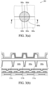
- FIG. 3(a) illustrates a top view of a semiconductor device 301 according to some embodiments of the present disclosure.
- the semiconductor device 301 illustrated in FIG. 3(a) is similar to that illustrated in FIG. 2(a) with a difference including that a side surface 303e of the first light sensing unit 303a is curved by which the portion of the first light sensing unit 303a surrounded by the second light sensing units 305a of the same pixel sensor may be further reduced compared to that illustrated in FIG. 2(a) .
- the portion of the first light sensing unit 303a surrounded by the second light sensing units 305a of the same pixel sensor is smaller than the portion of the first light sensing unit 303a surrounded by a first light sensing unit 303b, 303c, 303d.
- the portion of the first light sensing unit 303a surrounded by the second light sensing units 305a of the same pixel sensor may be further reduced, the crosstalk interference mentioned above is further reduced compared to that illustrated in FIG. 2(a) .
- FIG. 3(b) illustrates a cross-sectional view taken along line C-C' of the semiconductor device 301 in FIG. 3(a) .
- the structure of the semiconductor device 301 illustrated in FIG. 3(b) is similar to that illustrated in FIG. 2(b) , which are not further described for brevity.
- FIG. 4(a) illustrates a top view of a semiconductor device 401 according to some embodiments of the present disclosure.
- the semiconductor device 401 illustrated in FIG. 4(a) is similar to that illustrated in FIG. 2(a) with a difference including that an third light sensing unit 431a, 431b is disposed between the first light sensing unit 403a, 403b and the second light sensing unit 405a, 405b.
- FIG. 4(b) illustrates a cross-sectional view taken along line D-D' of the semiconductor device 401 in FIG. 4(a) .
- the third light sensing unit 431a, 431b is different from the first light sensing unit 403a, 403b and the second light sensing unit 405a, 405b so the third light sensing unit 431a, 431b could be distinguished from the first light sensing unit 403a, 403b and not cause a crosstalk as the second light sensing unit 405a, 405b does.
- the third light sensing unit 431a, 431b is operable to receive a radiation projected toward the third light sensing unit 431a, 431b and convert the radiation to electrical signal.
- the third light sensing unit 431a, 431b is operable to receive less radiation projected toward it than the first light sensing unit 403a, 403b, the second light sensing unit 405a, 405b, or both and convert the radiation to electrical signal.
- the third light sensing unit 431a, 431b may receive less radiation projected toward it than the second light sensing unit 405a, 405b, it may cause less crosstalk than the second light sensing unit 405a, 405b does, which further reduces the crosstalk interference toward the first light sensing unit 403a, 403b compared to a second light sensing unit 405a, 405b.
- the third light sensing unit 431a, 431b between the first light sensing unit 403a, 403b and the second light sensing unit 405a, 405b may increase the distance between them and make the crosstalk source of the second light sensing unit 405a, 405b to be away from the first light sensing unit 403a, 403b, less crosstalk may reach the first light sensing unit 403a, 403b, which further improves the sensitivity of the first light sensing unit 403a, 403b.
- FIG. 5 illustrates a cross-sectional view of a semiconductor device 501 according to some embodiments of the present disclosure.
- the semiconductor device 501 illustrated in FIG. 5 is similar to that illustrated in FIG. 1(a) , FIG. 2(a) , FIG. 3(a) , and FIG. 4(a) with a difference including that the first isolation structure 511a has a larger projection area compared to a regular design.
- a projection area of the first isolation structure 511b is enlarged compared to a regular design so less crosstalk transmits through it and reach the first light sensing unit 503a, 503b. As a result, the crosstalk interference from the neighboring second light sensing unit 505b is reduced.
- the crosstalk interference from the neighboring second light sensing unit 505b is reduced by disposing the first isolation structure 511b having a larger projection area than the second isolation structure 511a.
- the first isolation structure 511b includes a liner 507b and an insulating structure 509b.
- the second isolation structure 511a includes a liner 507a and an insulating structure 509a.
- the liners 507b, 507a and the insulation structures 509b, 509a are similar to those described above and are not further described for brevity.
- FIG. 6 illustrates a cross-sectional view of a semiconductor device 601 according to some embodiments of the present disclosure.
- the semiconductor device 601 illustrated in FIG. 6 is similar to that illustrated in FIG. 1(a) , FIG. 2(a) , FIG. 3(a) , and FIG. 4(a) with a difference including that the reflective layer 619 extends from a projection area of the first light sensing unit 603a to a projection area of a neighboring second light sensing unit 605b.
- the reflective layer 619 By disposing the reflective layer 619 extending from a projection area of the first light sensing unit 603a to a projection area of a neighboring second light sensing unit 605b, the reflective layer 619 reduces the light projected toward the second light sensing unit 605b and crosstalk generated from the first light sensing unit 603a. Nevertheless, it should be noted that embodiments of the extension of the reflective layer 619 are designed that the reduction of the light toward the second light sensing unit 605b by the reflective layer 619 does not affect the intended purpose of the second light sensing unit 605b as receiving more radiation than a first light sensing unit 603a.
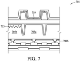
- FIG. 7 illustrates a cross-sectional view of a semiconductor device 701 according to some embodiments of the present disclosure.
- the semiconductor device 701 illustrated in FIG. 7 is similar to that illustrated in FIG. 1(a) , FIG. 2(a) , FIG. 3(a) , and FIG. 4(a) with a difference including that a first surface 733 of a second light sensing unit 705b has roughness.
- the second light sensing unit 705b has a first surface 733 facing the reflective layer 719 and a second surface 701b opposite to the first surface 733.
- the first surface 733 of the second light sensing unit 705b As having roughness compared to the first surface 101a of the semiconductor device 701, less light is transmitted through the semiconductor device 701 to reach the second light sensing unit 705b because some light is refracted or reflected by the roughed first surface 733 of the second light sensing unit 705b. As a result, since less light reaches the second light sensing unit 705b because of the roughed first surface 733, less crosstalk interference is generated toward the neighboring first light sensing unit 703a. Therefore, the sensitivity of the neighboring first light sensing unit 703a increases.
- the roughness of the first surface 733 of the second light sensing unit 705b is so designed that the reduction of the light toward the second light sensing unit 705b by the roughness of the first surface 733 does not affect the intended purpose of the second light sensing unit 705b as receiving more radiation than a first light sensing unit 703a.
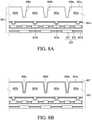
- FIGs. 8A-8H illustrate a method of manufacturing a semiconductor device such as the semiconductor device of FIG. 2(a), FIG. 2(b) , FIG. 3(a), and FIG. 3(b) .
- a substrate 801 is provided or received.
- the substrate 801 has a first surface 801a and a second surface 801b opposite to the first surface 801a.
- the substrate 801 is a bulk semiconductor substrate (e.g., a bulk silicon (Si) substrate), a silicon-on-insulator (SOI) substrate, or a wafer.
- the substrate 801 is a wafer.
- the substrate 801 includes a plurality of first light sensing units 803a, 803b and a plurality of second light sensing units 805a, 805b arranged in a sub-array adjacent to the first surface 801a of the substrate 801.
- the first light sensing units 803a, 803b and the second light sensing units 805a, 805b are so disposed that at least a portion of the first light sensing unit 803a is adjacent to at least one first light sensing unit 803b.
- the first light sensing units 803a, 803b are different from the second light sensing units 805a, 805b in that a surface of the second light sensing units 805a, 805b is roughened.
- a logic device 823a, 823b such as a transistor, may be further disposed to a third surface 801c opposite to the first surface 101a of the substrate 801.
- the logic device 823a, 823b is operable to enable readout of the first light sensing unit 803a, 803b, the second light sensing unit 805a, 805b, or both.
- the logic device 823a, 823b is disposed adjacent to the first light sensing unit 803a, 803b, the second light sensing unit 805a, 805b, or both.
- the logic device 823a, 823b is disposed adjacent to a third surface 801c opposite to the first surface 801a of the substrate 801 and close to the back end of the first light sensing unit 803a, 803b and the second light sensing unit 805a, 805b.
- a circuit stack 829 may be further disposed adjacent to the logic device 823a, 823b.
- the circuit stack 829 may be disposed adjacent to the second surface 801b of the substrate 801.
- the circuit stack 829 is a back-end-of-line (BEOL) metallization stack.
- circuit stack 829 electrically connects to the logic device 823a, 823b through at least one conductive via, at least one conductive contact, or a combination thereof.
- the circuit stack 829 includes at least one metal layer 827 and at least one dielectric layer 825.
- a trench 808c, 808b, 808a may be disposed between the first light sensing unit 803a and the second light sensing unit 805a, the first light sensing unit 803a and the first light sensing unit 803b, and the first light sensing unit 803b and the second light sensing unit 805b.
- trenches 808c, 808b, 808a have a substantially rectangular shape, a trapezoidal shape, an elongated elliptical shape, or any other suitable shape.
- trenches 808c, 808b, 808a are formed by an etching technology, a drilling technology (e.g., a mechanical or laser drilling technology), or any suitable technologies applied from the first surface 801a of the substrate 801 toward the second surface 801b of the substrate 801.
- a drilling technology e.g., a mechanical or laser drilling technology
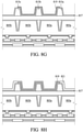
- a liner 807 is disposed adjacent to the first surface 801a of the substrate 801.
- the liner 807 is disposed in conformity with the shape of the trench 808c, 808b, 808a of the substrate 801.
- the liner 807 is formed by an atomic layer deposition (ALD) technology, a chemical vapor deposition (CVD) technology, or any suitable technologies.
- an insulating structure 809a, 809b, 809c is disposed adjacent to the liner 807.
- the insulating structure 809a, 809b, 809c fills the trench 808c, 808b, 808a of the substrate 801.
- the insulating structures 809a, 809b, 809c are disposed by an atomic layer deposition (ALD) technology, a chemical vapor deposition (CVD) technology, or any suitable technologies.
- a first dielectric layer 813 is disposed adjacent to the liner 807.
- the first dielectric layer 813 is disposed on the liner 807 and the insulating structure 809a, 809b, 809c.
- the first dielectric layer 813 is disposed by an atomic layer deposition (ALD) technology, a chemical vapor deposition (CVD) technology, or any suitable technologies.
- ALD atomic layer deposition
- CVD chemical vapor deposition
- a metal layer 815a, 815b, 815c is disposed adjacent to the first dielectric layer 813.
- the metal layers 815a, 815b, 815c are disposed corresponding to the portions of the first isolation structure 811a, 811b, 811c.
- the metal layers 815a, 815b, 815c are formed by a technology selected from a plating technology, a photolithography technology, a polishing technology, and an etching technology.
- a second dielectric layer 817 is disposed adjacent to the first dielectric layer 813.
- the second dielectric layer 817 is disposed on the metal layer 815a, 815b, 815c and the first dielectric layer 813.
- the second dielectric layer 817 is disposed by an atomic layer deposition (ALD) technology, a chemical vapor deposition (CVD) technology, or any suitable technologies.
- ALD atomic layer deposition
- CVD chemical vapor deposition
- a reflective layer 819 is disposed adjacent to the second dielectric layer 817.
- the reflective layer 819 is disposed at a position corresponding to the first light sensing units 803a, 803b, which defines the area of the first light sensing units 803a, 803b.
- the reflective layer 819 is disposed by a technology selected from a plating technology, a photolithography technology, a polishing technology, and an etching technology.
- a third dielectric layer 821 is disposed adjacent to the second dielectric layer 817.
- the third dielectric layer 821 is disposed over the reflective layer 819 and the second dielectric layer 817.
- the third dielectric layer 821 is disposed by an atomic layer deposition (ALD) technology, a chemical vapor deposition (CVD) technology, or any suitable technologies. Subsequently, a semiconductor device, such as the one illustrated in FIG. 2(b) and FIG. 3(b) are obtained.
- a singularizing process is further performed on the semiconductor device obtained from the process mentioned above to obtain an image sensor including at least one pixel sensor including a first light sensing unit 803a and a second light sensing unit 805a arranged in a sub-array with the first light sensing unit 803a, where at least a portion of the first light sensing unit 803a is adjacent to at least one first light sensing unit 803b of another pixel sensor.
- a semiconductor device in some embodiments, includes a plurality of first light sensing units and a plurality of second light sensing units arranged in a sub-array with the first light sensing units, where the first light sensing unit refers to a light sensing unit that is operable to receive less radiation compared to the second light sensing unit and at least a portion of the first light sensing unit is adjacent to at least one first light sensing unit.
- a semiconductor image sensor includes a pixel sensor comprising a first light sensing unit and a second light sensing unit arranged in a sub-array with the first light sensing unit, where the first light sensing unit refers to a light sensing unit that is operable to receive less radiation compared to a second light sensing unit and at least a portion of the first light sensing unit is adjacent to at least one first light sensing unit of another pixel sensor.
- a method of manufacturing a semiconductor device includes: providing a substrate having a first surface and a second surface opposite to the first surface; disposing a plurality of first light sensing units and a plurality of second light sensing units arranged in a sub-array adjacent to the first surface of the substrate, where the first light sensing unit refers to a light sensing unit that is operable to receive less radiation compared to a second light sensing unit and at least a portion of the first light sensing unit is adjacent to at least one first light sensing unit; disposing a first isolation structure between the first light sensing unit and the second light sensing unit and a second isolation structure disposed between the adjacent first light sensing units; and disposing a reflective layer above the first light sensing unit.
Landscapes
- Solid State Image Pick-Up Elements (AREA)
- Transforming Light Signals Into Electric Signals (AREA)
- Light Receiving Elements (AREA)
- Photometry And Measurement Of Optical Pulse Characteristics (AREA)
Abstract
Description
- Semiconductor image sensors are used for sensing light. The semiconductor image sensors utilize an array of pixels in a substrate, including photodiodes and transistors that can absorb radiation projected toward the substrate and convert the sensed radiation into electrical signals.
- A performance of a semiconductor image sensor depends on, among other things, its quantum efficiency and optical crosstalk. The quantum efficiency of an image sensor indicates a number of electrons generated per number of incident photons in the image sensor. The optical crosstalk occurs when some photons incident upon a pixel are absorbed by another pixel.
- Therefore, while existing semiconductor structures of image sensors and conventional methods of manufacturing image sensors have been generally adequate for their intended purposes, they have not been entirely satisfactory in every aspect.
- Aspects of the present disclosure are best understood from the following detailed description when read with the accompanying figures. It is noted that, in accordance with the standard practice in the industry, various features are not drawn to scale. In fact, the dimensions of the various features may be arbitrarily increased or reduced for clarity of discussion.
-
FIG. 1 (a) illustrates a top view of a semiconductor device according to some embodiments of the present disclosure.FIG. 1(b) illustrates a cross-sectional view taken along line A-A' of the semiconductor device inFIG. 1(a) . -
FIG. 2(a) illustrates a top view of a semiconductor device according to some embodiments of the present disclosure.FIG. 2(b) illustrates a cross-sectional view taken along line B-B' of the semiconductor device inFIG. 2(a) . -
FIG. 3(a) illustrates a top view of a semiconductor device according to some embodiments of the present disclosure.FIG. 3(b) illustrates a cross-sectional view taken along line C-C' of the semiconductor device inFIG. 3(a) . -
FIG. 4(a) illustrates a top view of a semiconductor device according to some embodiments of the present disclosure.FIG. 4(b) illustrates a cross-sectional view taken along line D-D' of the semiconductor device inFIG. 4(a) . -
FIG. 5 illustrates a cross-sectional view of a semiconductor device according to some embodiments of the present disclosure. -
FIG. 6 illustrates a cross-sectional view of a semiconductor device according to some embodiments of the present disclosure. -
FIG. 7 illustrates a cross-sectional view of a semiconductor device according to some embodiments of the present disclosure. -
FIG. 8A, FIG. 8B ,FIG. 8C, FIG. 8D ,FIG. 8E, FIG. 8F ,FIG. 8G, and FIG. 8H illustrate a method of manufacturing a semiconductor device such as the semiconductor device ofFIG. 2(a), FIG. 2(b) ,FIG. 3(a), and FIG. 3(b) . - The following disclosure provides many different embodiments, or examples, for implementing different features of the provided subject matter. Specific examples of elements and arrangements are described below to simplify the present disclosure. These are, of course, merely examples and are not intended to be limiting. For example, the formation of a first feature over or on a second feature in the description that follows may include embodiments in which the first and second features are formed in direct contact, and may also include embodiments in which additional features may be formed between the first and second features, such that the first and second features may not be in direct contact. In addition, the present disclosure may repeat reference numerals and/or letters in the various examples. This repetition is for the purpose of simplicity and clarity and does not in itself dictate a relationship between the various embodiments and/or configurations discussed.
- Further, spatially relative terms, such as "beneath," "below," "lower," "above," "upper," "on" and the like, may be used herein for ease of description to describe one element or feature's relationship to another element(s) or feature(s) as illustrated in the figures. The spatially relative terms are intended to encompass different orientations of the device in use or operation in addition to the orientation depicted in the figures. The apparatus may be otherwise oriented (rotated 90 degrees or at other orientations) and the spatially relative descriptors used herein may likewise be interpreted accordingly.
- As used herein, the terms such as "first," "second," and "third" describe various elements, components, regions, layers and/or sections, these elements, components, regions, layers and/or sections should not be limited by these terms. These terms may be only used to distinguish one element, component, region, layer or section from another. The terms such as "first," "second," and "third" when used herein do not imply a sequence or order unless clearly indicated by the context.
- As used herein, the terms "approximately," "substantially," "substantial," and "about" are used to describe and account for small variations. When used in conjunction with an event or circumstance, the terms can refer to instances in which the event or circumstance occurs precisely as well as instances in which the event or circumstance occurs to a close approximation. For example, when used in conjunction with a numerical value, the terms can refer to a range of variation of less than or equal to ±10% of that numerical value, such as less than or equal to ±5%, less than or equal to ±4%, less than or equal to ±3%, less than or equal to ±2%, less than or equal to ±1%, less than or equal to ±0.5%, less than or equal to ±0.1%, or less than or equal to ±0.05%. For example, two numerical values can be deemed to be "substantially" the same or equal if a difference between the values is less than or equal to ±10% of an average of the values, such as less than or equal to ±5%, less than or equal to ±4%, less than or equal to ±13%, less than or equal to ±2%, less than or equal to ±1%, less than or equal to ±0.5%, less than or equal to ±0.1%, or less than or equal to ±0.05%. For example, "substantially" parallel can refer to a range of angular variation relative to 0° that is less than or equal to ±10°, such as less than or equal to ±5°, less than or equal to ±4°, less than or equal to ±3°, less than or equal to ±2°, less than or equal to ±1°, less than or equal to ±0.5°, less than or equal to ±0.1°, or less than or equal to ±0.05°. For example, "substantially" perpendicular can refer to a range of angular variation relative to 90° that is less than or equal to ±10°, such as less than or equal to ±5°, less than or equal to ±4°, less than or equal to ±3°, less than or equal to ±2°, less than or equal to ±1°, less than or equal to ±0.5°, less than or equal to ±0.1°, or less than or equal to ±0.05°.
- Some embodiments of image sensors use at least two kinds of pixel sensors, classified by the incident radiation, forming a repeating unit arranged in an array. For example, some embodiments of an image sensor include a first pixel sensor for sensing long wavelengths (e.g., infrared (IR) and red light) and a second pixel sensor for sensing short wavelengths (e.g., green and blue light). In addition, in some embodiments, each of the pixel sensors further use at least two kinds of light sensing units, classified by the amount of the incident radiation (or light) to be received. For example, as used herein, a first light sensing unit refers to a light sensing unit that is operable to receive less radiation (or light) compared to a second light sensing unit given a certain period of time.
- As the size of an image sensor gets smaller, crosstalk becomes a major concern between neighboring pixel sensors and further the neighboring light sensing units contained in the neighboring pixel sensors. As the surface area for receiving light becomes smaller, the light sensing unit becomes more sensitive to crosstalk because the signal (light directly received by the sensor) is smaller in comparison to the noise (the crosstalk between neighboring pixel sensors). Crosstalk adversely affects the amount of the light that is received by the light sensing unit. Pixel sensor designs which reduce crosstalk provide increased light absorption efficiency, especially beneficial for low levels of incident light.
-
FIG. 1(a) illustrates a top view of asemiconductor device 101 according to some embodiments of the present disclosure.FIG. 1(b) illustrates a cross-sectional view taken along line A-A' of thesemiconductor device 101 inFIG. 1(a) . - The
semiconductor device 101 ofFIG. 1(a) includes a plurality of firstlight sensing units light sensing units - The
semiconductor device 101 has afirst surface 101a and asecond surface 101b opposite to thefirst surface 101a. According to some embodiments,semiconductor device 101 is a bulk semiconductor substrate (e.g., a bulk silicon (Si) substrate), a silicon-on-insulator (SOI) substrate, or a wafer. In some embodiments, thesemiconductor device 101 is a wafer. - The first
light sensing unit light sensing unit light sensing unit light sensing unit light sensing unit - The second
light sensing unit light sensing unit light sensing unit light sensing unit light sensing unit light sensing unit light sensing unit light sensing unit reflective layer 119 above the firstlight sensing unit light sensing unit light sensing unit light sensing unit - The first
light sensing unit light sensing unit light sensing unit light sensing unit light sensing unit light sensing units light sensing unit light sensing units light sensing unit light sensing unit light sensing unit light sensing units light sensing units light sensing unit light sensing units light sensing unit light sensing units light sensing unit light sensing units - According to some embodiments, a pixel sensor composed of the first
light sensing unit 103a and the secondlight sensing units - According to some embodiments, a
first isolation structure light sensing unit light sensing unit light sensing unit light sensing unit light sensing unit light sensing unit first isolation structure first isolation structure liner structure - The
liner trench first surface 101a of thesemiconductor device 101. - In some embodiments, the
liner light sensing unit 103a, a high-k (high dielectric constant) material, or a combination thereof. In some embodiments, the low-n material includes, for example, SiO2, HfO2, or a combination thereof. In some embodiments, the high-k material includes, for example, HfO2, Al2O3, TiO2, HfZrO, Ta2O3, Ta2O5, HfSiO4, ZrO2, ZrSiO2, Ln2O3, or a combination thereof. - The insulating
structure liner structure liner structure light sensing unit 103a. In some embodiments, the low-n material includes, for example, SiO2, HfO2, or a combination thereof. In some embodiments, the insulatingstructure insulation structure insulation structure light sensing unit light sensing unit - A
logic device semiconductor device 101 and operable to enable readout of the firstlight sensing unit light sensing unit logic device light sensing unit light sensing unit logic device third surface 101c opposite to thefirst surface 101a of thesemiconductor device 101 and close to the back end of the firstlight sensing unit light sensing unit - According to some embodiments, the
circuit stack 129 is further disposed adjacent to thelogic device circuit stack 129 is disposed adjacent to thesecond surface 101b of thesemiconductor device 101. In some embodiments,circuit stack 129 is a back-end-of-line (BEOL) metallization stack. In some embodiments,circuit stack 129 electrically connects to thelogic device circuit stack 129 includes at least onemetal layer 127 and at least onedielectric layer 125. - The
metal layer 127 is disposed in thedielectric layer 125. In some embodiments, themetal layer 127 includes, for example, copper, tungsten, aluminum, other metals, or a metal alloy thereof. - According to some embodiments,
dielectric layer 125 includes a low-k material (e.g., a dielectric material having a dielectric constant less than 3.9). -
FIG. 2(a) illustrates a top view of asemiconductor device 201 according to some embodiments of the present disclosure. Thesemiconductor device 201 illustrated inFIG. 2(a) is similar to that illustrated inFIG. 1(a) with a difference including that at least a portion of a firstlight sensing units 203a is adjacent to at least one firstlight sensing unit FIG. 2(b) illustrates a cross-sectional view taken along line B-B' of thesemiconductor device 201 inFIG. 2(a) . - Unlike the
semiconductor device 101 illustrated inFIG. 1(a) and FIG. 1(b) , thesemiconductor device 201 illustrated inFIG. 2(a) and FIG. 2(b) includes at least one firstlight sensing unit 203a disposed adjacent to at least one firstlight sensing unit light sensing unit 203a is disposed adjacent to at least one firstlight sensing unit light sensing unit 203a is disposed adjacent to at least one firstlight sensing unit light sensing unit 203a may be adjoined at a first side by a second instance of the firstlight sensing unit 203b, and at a second side adjacent to the first side by a third first type oflight sensing unit 203d. In some embodiments, at least a portion of the firstlight sensing unit 203a is surrounded by at least one firstlight sensing unit light sensing unit 203a is surrounded by at least two firstlight sensing units light sensing unit 203a is surrounded by at least three firstlight sensing units - At least a portion of the first
light sensing unit 203a is surrounded by at least a portion of another firstlight sensing unit light sensing unit 203a is surrounded by at least a portion of a secondlight sensing unit 205a. In some embodiments, at least a portion of the firstlight sensing unit 203a is surrounded by at least a portion of another firstlight sensing unit light sensing unit 203a is surrounded by at least a portion of a secondlight sensing unit 205a. - In some embodiments, the first
light sensing unit 203a and the secondlight sensing unit 205a constitute a pixel sensor. According to some embodiments, a pixel sensor includes at least one firstlight sensing unit 203a and at least one secondlight sensing unit 205a. In some embodiments, the firstlight sensing unit 203a is adjacent to at least one secondlight sensing unit 205a. In some embodiments, the firstlight sensing unit 203a is disposed adjacent to one, two, three, four, or five secondlight sensing units light sensing unit 203a is surrounded by the secondlight sensing unit light sensing unit 203a is surrounded by at least one secondlight sensing unit 205a in a pixel sensor. In some embodiments, a repeating pixel sensor unit includes a firstlight sensing unit 203a surrounded by a secondlight sensing unit 205a. In some embodiments, the firstlight sensing unit 203a is disposed adjacent to a corner of a pixel sensor. In some embodiments, the firstlight sensing unit 203a is located at a corner of a pixel sensor. In some embodiments, a projection area of the firstlight sensing unit light sensing unit - In some embodiments, a first
light sensing unit 203a is surrounded by one secondlight sensing units 205a of the same pixel sensor and by another secondlight sensing unit light sensing unit 203a surrounded by the secondlight sensing units 205a of the same pixel sensor is not greater than the portion of the firstlight sensing unit 203a surrounded by a firstlight sensing unit - By disposing at least a portion of a first
light sensing units 203a adjacent to at least one firstlight sensing unit 203b, the crosstalk occurred due to the reflection or refraction of the light from the neighboring secondlight sensing unit 205a to the firstlight sensing units 203a is reduced as the area of the secondlight sensing unit 205b surrounding the firstlight sensing unit 203a is reduced. As a result, since the light interference (e.g., crosstalk) from the neighboring secondlight sensing unit light sensing units - Referring to
FIG. 2(b) , in some embodiments where a firstlight sensing unit 203a is disposed adjacent to another firstlight sensing unit 203b, thereflective layer 219 extends from a projection area of the firstlight sensing unit 203a to a projection area of the firstlight sensing unit 203b. -
FIG. 3(a) illustrates a top view of asemiconductor device 301 according to some embodiments of the present disclosure. Thesemiconductor device 301 illustrated inFIG. 3(a) is similar to that illustrated inFIG. 2(a) with a difference including that aside surface 303e of the firstlight sensing unit 303a is curved by which the portion of the firstlight sensing unit 303a surrounded by the secondlight sensing units 305a of the same pixel sensor may be further reduced compared to that illustrated inFIG. 2(a) . In some embodiments, the portion of the firstlight sensing unit 303a surrounded by the secondlight sensing units 305a of the same pixel sensor is smaller than the portion of the firstlight sensing unit 303a surrounded by a firstlight sensing unit light sensing unit 303a surrounded by the secondlight sensing units 305a of the same pixel sensor may be further reduced, the crosstalk interference mentioned above is further reduced compared to that illustrated inFIG. 2(a) . -
FIG. 3(b) illustrates a cross-sectional view taken along line C-C' of thesemiconductor device 301 inFIG. 3(a) . The structure of thesemiconductor device 301 illustrated inFIG. 3(b) is similar to that illustrated inFIG. 2(b) , which are not further described for brevity. -
FIG. 4(a) illustrates a top view of asemiconductor device 401 according to some embodiments of the present disclosure. Thesemiconductor device 401 illustrated inFIG. 4(a) is similar to that illustrated inFIG. 2(a) with a difference including that an thirdlight sensing unit light sensing unit light sensing unit FIG. 4(b) illustrates a cross-sectional view taken along line D-D' of thesemiconductor device 401 inFIG. 4(a) . - In some embodiments, the third
light sensing unit light sensing unit light sensing unit light sensing unit light sensing unit light sensing unit light sensing unit light sensing unit light sensing unit light sensing unit light sensing unit light sensing unit light sensing unit light sensing unit light sensing unit light sensing unit - In addition, since disposing the third
light sensing unit light sensing unit light sensing unit light sensing unit light sensing unit light sensing unit light sensing unit -
FIG. 5 illustrates a cross-sectional view of asemiconductor device 501 according to some embodiments of the present disclosure. Thesemiconductor device 501 illustrated inFIG. 5 is similar to that illustrated inFIG. 1(a) ,FIG. 2(a) ,FIG. 3(a) , andFIG. 4(a) with a difference including that thefirst isolation structure 511a has a larger projection area compared to a regular design. - In some embodiments, such as those illustrated in
FIG. 1(b) where thefirst isolation structure 511b is disposed separating the firstlight sensing unit 503a from the secondlight sensing unit 505b, a projection area of thefirst isolation structure 511b is enlarged compared to a regular design so less crosstalk transmits through it and reach the firstlight sensing unit 503a, 503b. As a result, the crosstalk interference from the neighboring secondlight sensing unit 505b is reduced. - In some embodiments, such as those illustrated in
FIG. 2(b) ,3(b) , and4(b) where afirst isolation structure 511b is disposed separating the firstlight sensing unit 503a from the secondlight sensing unit 505b and asecond isolation structure 511a is disposed separating the firstlight sensing unit 503a from another first light sensing unit 503b, the crosstalk interference from the neighboring secondlight sensing unit 505b is reduced by disposing thefirst isolation structure 511b having a larger projection area than thesecond isolation structure 511a. - In some embodiments, the
first isolation structure 511b includes aliner 507b and an insulatingstructure 509b. In some embodiments, thesecond isolation structure 511a includes aliner 507a and an insulatingstructure 509a. Theliners insulation structures -
FIG. 6 illustrates a cross-sectional view of asemiconductor device 601 according to some embodiments of the present disclosure. Thesemiconductor device 601 illustrated inFIG. 6 is similar to that illustrated inFIG. 1(a) ,FIG. 2(a) ,FIG. 3(a) , andFIG. 4(a) with a difference including that thereflective layer 619 extends from a projection area of the firstlight sensing unit 603a to a projection area of a neighboring secondlight sensing unit 605b. - By disposing the
reflective layer 619 extending from a projection area of the firstlight sensing unit 603a to a projection area of a neighboring secondlight sensing unit 605b, thereflective layer 619 reduces the light projected toward the secondlight sensing unit 605b and crosstalk generated from the firstlight sensing unit 603a. Nevertheless, it should be noted that embodiments of the extension of thereflective layer 619 are designed that the reduction of the light toward the secondlight sensing unit 605b by thereflective layer 619 does not affect the intended purpose of the secondlight sensing unit 605b as receiving more radiation than a firstlight sensing unit 603a. -
FIG. 7 illustrates a cross-sectional view of asemiconductor device 701 according to some embodiments of the present disclosure. Thesemiconductor device 701 illustrated inFIG. 7 is similar to that illustrated inFIG. 1(a) ,FIG. 2(a) ,FIG. 3(a) , andFIG. 4(a) with a difference including that afirst surface 733 of a secondlight sensing unit 705b has roughness. - The second
light sensing unit 705b has afirst surface 733 facing thereflective layer 719 and asecond surface 701b opposite to thefirst surface 733. - By disposing the
first surface 733 of the secondlight sensing unit 705b as having roughness compared to thefirst surface 101a of thesemiconductor device 701, less light is transmitted through thesemiconductor device 701 to reach the secondlight sensing unit 705b because some light is refracted or reflected by the roughedfirst surface 733 of the secondlight sensing unit 705b. As a result, since less light reaches the secondlight sensing unit 705b because of the roughedfirst surface 733, less crosstalk interference is generated toward the neighboring firstlight sensing unit 703a. Therefore, the sensitivity of the neighboring firstlight sensing unit 703a increases. It should be noted that the roughness of thefirst surface 733 of the secondlight sensing unit 705b is so designed that the reduction of the light toward the secondlight sensing unit 705b by the roughness of thefirst surface 733 does not affect the intended purpose of the secondlight sensing unit 705b as receiving more radiation than a firstlight sensing unit 703a. -
FIGs. 8A-8H illustrate a method of manufacturing a semiconductor device such as the semiconductor device ofFIG. 2(a), FIG. 2(b) ,FIG. 3(a), and FIG. 3(b) . - Referring to
FIG. 8A , asubstrate 801 is provided or received. Thesubstrate 801 has afirst surface 801a and asecond surface 801b opposite to thefirst surface 801a. In some embodiments, thesubstrate 801 is a bulk semiconductor substrate (e.g., a bulk silicon (Si) substrate), a silicon-on-insulator (SOI) substrate, or a wafer. In some embodiments, thesubstrate 801 is a wafer. - The
substrate 801 includes a plurality of firstlight sensing units light sensing units first surface 801a of thesubstrate 801. The firstlight sensing units light sensing units light sensing unit 803a is adjacent to at least one firstlight sensing unit 803b. In some embodiments, the firstlight sensing units light sensing units light sensing units - A
logic device third surface 801c opposite to thefirst surface 101a of thesubstrate 801. Thelogic device light sensing unit light sensing unit logic device light sensing unit light sensing unit logic device third surface 801c opposite to thefirst surface 801a of thesubstrate 801 and close to the back end of the firstlight sensing unit light sensing unit - A
circuit stack 829 may be further disposed adjacent to thelogic device circuit stack 829 may be disposed adjacent to thesecond surface 801b of thesubstrate 801. In some embodiments, thecircuit stack 829 is a back-end-of-line (BEOL) metallization stack. According to some embodiments,circuit stack 829 electrically connects to thelogic device circuit stack 829 includes at least onemetal layer 827 and at least onedielectric layer 825. - Still referring to
FIG. 8A , atrench light sensing unit 803a and the secondlight sensing unit 805a, the firstlight sensing unit 803a and the firstlight sensing unit 803b, and the firstlight sensing unit 803b and the secondlight sensing unit 805b. In some embodiments,trenches - In some embodiments,
trenches first surface 801a of thesubstrate 801 toward thesecond surface 801b of thesubstrate 801. - Referring to
FIG. 8B , aliner 807 is disposed adjacent to thefirst surface 801a of thesubstrate 801. Theliner 807 is disposed in conformity with the shape of thetrench substrate 801. In some embodiments, theliner 807 is formed by an atomic layer deposition (ALD) technology, a chemical vapor deposition (CVD) technology, or any suitable technologies. - Referring to
FIG. 8C , an insulatingstructure liner 807. In some embodiments, the insulatingstructure trench substrate 801. In some embodiments, the insulatingstructures - Referring to
FIG. 8D , a firstdielectric layer 813 is disposed adjacent to theliner 807. In some embodiments, thefirst dielectric layer 813 is disposed on theliner 807 and the insulatingstructure first dielectric layer 813 is disposed by an atomic layer deposition (ALD) technology, a chemical vapor deposition (CVD) technology, or any suitable technologies. - Referring to
FIG. 8E , ametal layer first dielectric layer 813. In some embodiments, themetal layers first isolation structure metal layers - Referring to
FIG. 8F , asecond dielectric layer 817 is disposed adjacent to thefirst dielectric layer 813. In some embodiments, thesecond dielectric layer 817 is disposed on themetal layer first dielectric layer 813. In some embodiments, thesecond dielectric layer 817 is disposed by an atomic layer deposition (ALD) technology, a chemical vapor deposition (CVD) technology, or any suitable technologies. - Referring to
FIG. 8G , areflective layer 819 is disposed adjacent to thesecond dielectric layer 817. Thereflective layer 819 is disposed at a position corresponding to the firstlight sensing units light sensing units reflective layer 819 is disposed by a technology selected from a plating technology, a photolithography technology, a polishing technology, and an etching technology. - Referring to
FIG. 8H , a thirddielectric layer 821 is disposed adjacent to thesecond dielectric layer 817. In some embodiments, the thirddielectric layer 821 is disposed over thereflective layer 819 and thesecond dielectric layer 817. In some embodiments, the thirddielectric layer 821 is disposed by an atomic layer deposition (ALD) technology, a chemical vapor deposition (CVD) technology, or any suitable technologies. Subsequently, a semiconductor device, such as the one illustrated inFIG. 2(b) andFIG. 3(b) are obtained. - In some embodiments, a singularizing process is further performed on the semiconductor device obtained from the process mentioned above to obtain an image sensor including at least one pixel sensor including a first
light sensing unit 803a and a secondlight sensing unit 805a arranged in a sub-array with the firstlight sensing unit 803a, where at least a portion of the firstlight sensing unit 803a is adjacent to at least one firstlight sensing unit 803b of another pixel sensor. - In some embodiments, a semiconductor device is provided. The semiconductor device includes a plurality of first light sensing units and a plurality of second light sensing units arranged in a sub-array with the first light sensing units, where the first light sensing unit refers to a light sensing unit that is operable to receive less radiation compared to the second light sensing unit and at least a portion of the first light sensing unit is adjacent to at least one first light sensing unit.
- In some embodiments, a semiconductor image sensor is provided. The semiconductor image sensor includes a pixel sensor comprising a first light sensing unit and a second light sensing unit arranged in a sub-array with the first light sensing unit, where the first light sensing unit refers to a light sensing unit that is operable to receive less radiation compared to a second light sensing unit and at least a portion of the first light sensing unit is adjacent to at least one first light sensing unit of another pixel sensor.
- In some embodiments, a method of manufacturing a semiconductor device is provided. The method includes: providing a substrate having a first surface and a second surface opposite to the first surface; disposing a plurality of first light sensing units and a plurality of second light sensing units arranged in a sub-array adjacent to the first surface of the substrate, where the first light sensing unit refers to a light sensing unit that is operable to receive less radiation compared to a second light sensing unit and at least a portion of the first light sensing unit is adjacent to at least one first light sensing unit; disposing a first isolation structure between the first light sensing unit and the second light sensing unit and a second isolation structure disposed between the adjacent first light sensing units; and disposing a reflective layer above the first light sensing unit.
- The foregoing outlines features of several embodiments so that those skilled in the art may better understand the aspects of the present disclosure. Those skilled in the art should appreciate that they may readily use the present disclosure as a basis for designing or modifying other processes and structures for carrying out the same purposes and/or achieving the same advantages of the embodiments introduced herein. Those skilled in the art should also realize that such equivalent constructions do not depart from the spirit and scope of the present disclosure, and that they may make various changes, substitutions, and alterations herein without departing from the spirit and scope of the present disclosure.
Claims (7)
- A semiconductor device, comprising:a plurality of a first type of light sensing units, wherein each of the plurality of the first type of light sensing units is operable to receive a first amount of radiation; anda plurality of a second type of light sensing units, wherein each of the plurality of the second type of light sensing units is operable to receive a second amount of radiation, and the plurality of the second type of light sensing units is arranged in an array with the plurality of the first type of light sensing units to form a pixel sensor, whereinthe first amount of radiation is smaller than the second amount of radiation, andat least a portion of a first instance of the first type of light sensing unit of the plurality of the first type of light sensing units is adjacent to a second instance of the first type of light sensing unit of the plurality of the first type of light sensing units.
- The semiconductor device of claim 1, whereina first portion of the first instance of the first type of light sensing unit is surrounded by a first second light sensing unit of the plurality of the second type of light sensing units, anda second portion of the first instance of the first type of light sensing unit is surrounded by the second instance of the first type of light sensing unit, andthe first portion is not greater than the second portion.
- The semiconductor device of claim 1, wherein the plurality of the second type of light sensing units is a circular region surrounded by the plurality of the first type of light sensing units.
- The semiconductor device of claim 1, further comprising a reflective layer above the plurality of the first type of light sensing units.
- The semiconductor device of claim 4, wherein the reflective layer extends from a projection area of one of the plurality of the first type of light sensing units to a projection area of one of the plurality of the second type of light sensing units.
- The semiconductor device of claim 1, further comprising:a first isolation structure between one of the plurality of the first type of light sensing units and one of the plurality of the second type of light sensing units; anda second isolation structure between adjacent first type of light sensing units of the plurality of the first type of light sensing units, wherein the first isolation structure has a larger projection area than the second isolation structure.
- The semiconductor device of claim 1, further comprising a third type of light sensing unit between one of the plurality of the first type of light sensing units and one of the plurality of the second type of light sensing units, wherein the third type of light sensing unit is operable to receive less radiation than the first amount of radiation or the second amount of radiation.
Applications Claiming Priority (2)
| Application Number | Priority Date | Filing Date | Title |
|---|---|---|---|
| US202063053094P | 2020-07-17 | 2020-07-17 | |
| US17/220,212 US12255217B2 (en) | 2020-07-17 | 2021-04-01 | Semiconductor device, semiconductor image sensor, and method of manufacturing the same |
Publications (2)
| Publication Number | Publication Date |
|---|---|
| EP3940782A2 true EP3940782A2 (en) | 2022-01-19 |
| EP3940782A3 EP3940782A3 (en) | 2022-02-23 |
Family
ID=76958800
Family Applications (1)
| Application Number | Title | Priority Date | Filing Date |
|---|---|---|---|
| EP21186093.7A Withdrawn EP3940782A3 (en) | 2020-07-17 | 2021-07-16 | Semiconductor device, semiconductor image sensor, and method of manufacturing the same |
Country Status (7)
| Country | Link |
|---|---|
| US (3) | US12255217B2 (en) |
| EP (1) | EP3940782A3 (en) |
| JP (1) | JP2022019687A (en) |
| KR (1) | KR102558318B1 (en) |
| CN (1) | CN113594192B (en) |
| DE (1) | DE102021108586A1 (en) |
| TW (1) | TWI794816B (en) |
Family Cites Families (18)
| Publication number | Priority date | Publication date | Assignee | Title |
|---|---|---|---|---|
| US6285031B1 (en) * | 1998-12-18 | 2001-09-04 | Isp Investments Inc. | Radiation dosimetry method and associated apparatus |
| US20070001100A1 (en) | 2005-06-30 | 2007-01-04 | Taiwan Semiconductor Manufacturing Company, Ltd. | Light reflection for backside illuminated sensor |
| TWI398707B (en) | 2008-05-16 | 2013-06-11 | 友達光電股份有限公司 | Light sensing unit and pixel structure and liquid crystal display panel having the same |
| JP5653829B2 (en) * | 2011-04-25 | 2015-01-14 | 富士フイルム株式会社 | Radiographic apparatus, radiographic system, and radiographic method |
| JP5788738B2 (en) * | 2011-08-26 | 2015-10-07 | 富士フイルム株式会社 | Manufacturing method of radiation detector |
| JP5592962B2 (en) * | 2012-02-03 | 2014-09-17 | 富士フイルム株式会社 | Radiation imaging apparatus, control method therefor, and radiation imaging system |
| EP2648404B1 (en) * | 2012-04-02 | 2016-12-07 | Harvest Imaging bvba | Floating diffusion pre-charge |
| JP6325650B2 (en) * | 2013-04-24 | 2018-05-16 | コーニンクレッカ フィリップス エヌ ヴェKoninklijke Philips N.V. | Radiation detection apparatus having photodetector pixel array, PET imaging system, optical photon addition method, and computer program for executing steps of optical photon addition method |
| JP2014122903A (en) * | 2013-12-20 | 2014-07-03 | Fujifilm Corp | Radiation detector and radiation imaging device |
| US9666631B2 (en) * | 2014-05-19 | 2017-05-30 | Omnivision Technologies, Inc. | Photodiode and filter configuration for high dynamic range image sensor |
| ITUB20169957A1 (en) | 2016-01-13 | 2017-07-13 | Lfoundry Srl | METHOD FOR MANUFACTURING NIR CMOS PERFORMED SENSORS |
| FR3056333B1 (en) * | 2016-09-22 | 2018-10-19 | Stmicroelectronics (Crolles 2) Sas | ENHANCED QUANTUM EFFICIENT IMAGE SENSOR FOR INFRARED RADIATION |
| US10770505B2 (en) | 2017-04-05 | 2020-09-08 | Intel Corporation | Per-pixel performance improvement for combined visible and ultraviolet image sensor arrays |
| US12009379B2 (en) * | 2017-05-01 | 2024-06-11 | Visera Technologies Company Limited | Image sensor |
| US10411063B2 (en) * | 2017-06-20 | 2019-09-10 | Omnivision Technologies, Inc. | Single-exposure high dynamic range sensor |
| US10312279B2 (en) | 2017-10-31 | 2019-06-04 | Semiconductor Components Industries, Llc | High dynamic range pixel with in-pixel light shield structures |
| JP7366751B2 (en) * | 2017-11-09 | 2023-10-23 | ソニーセミコンダクタソリューションズ株式会社 | Solid-state imaging devices and electronic equipment |
| US10790326B2 (en) | 2018-09-26 | 2020-09-29 | Taiwan Semiconductor Manufacturing Company, Ltd. | Pixel device on deep trench isolation (DTI) structure for image sensor |
-
2021
- 2021-04-01 US US17/220,212 patent/US12255217B2/en active Active
- 2021-04-07 DE DE102021108586.1A patent/DE102021108586A1/en active Pending
- 2021-05-18 TW TW110117922A patent/TWI794816B/en active
- 2021-05-31 KR KR1020210070176A patent/KR102558318B1/en active Active
- 2021-07-16 EP EP21186093.7A patent/EP3940782A3/en not_active Withdrawn
- 2021-07-16 JP JP2021117808A patent/JP2022019687A/en active Pending
- 2021-07-19 CN CN202110811899.5A patent/CN113594192B/en active Active
-
2023
- 2023-08-10 US US18/448,093 patent/US20230402480A1/en active Pending
-
2025
- 2025-07-15 US US19/269,356 patent/US20250344540A1/en active Pending
Also Published As
| Publication number | Publication date |
|---|---|
| DE102021108586A1 (en) | 2022-01-20 |
| EP3940782A3 (en) | 2022-02-23 |
| US20250344540A1 (en) | 2025-11-06 |
| US20220020787A1 (en) | 2022-01-20 |
| TW202218140A (en) | 2022-05-01 |
| KR20220010421A (en) | 2022-01-25 |
| KR102558318B1 (en) | 2023-07-20 |
| CN113594192B (en) | 2025-07-29 |
| TWI794816B (en) | 2023-03-01 |
| CN113594192A (en) | 2021-11-02 |
| US20230402480A1 (en) | 2023-12-14 |
| US12255217B2 (en) | 2025-03-18 |
| JP2022019687A (en) | 2022-01-27 |
Similar Documents
| Publication | Publication Date | Title |
|---|---|---|
| US10797096B2 (en) | Semiconductor image sensor | |
| US12356749B2 (en) | Image sensor device | |
| US11699718B2 (en) | Semiconductor image sensor | |
| US20220130881A1 (en) | Image sensor device having a first lens and a second lens over the first lens | |
| US11121166B2 (en) | Image sensor device | |
| US7524690B2 (en) | Image sensor with a waveguide tube and a related fabrication method | |
| TWI429067B (en) | Solid-state imaging element | |
| US9478575B2 (en) | Solid-state image sensor | |
| TWI399849B (en) | Solid-state imaging device, method of manufacturing solid-state imaging device, and electronic device | |
| US9691809B2 (en) | Backside illuminated image sensor device having an oxide film and method of forming an oxide film of a backside illuminated image sensor device | |
| KR20190055732A (en) | Color filter uniformity for image sensor devices | |
| US9627426B2 (en) | Image sensor device and method for forming the same | |
| US20180227521A1 (en) | Stacked image sensor pixel cell with in-pixel vertical channel transfer transistor and reflective structure | |
| KR20200037967A (en) | Image sensor | |
| US20240096917A1 (en) | Image sensor structure and method for forming the same | |
| CN113594192B (en) | Semiconductor device, semiconductor image sensor and manufacturing method thereof | |
| US11676982B2 (en) | Image sensing device | |
| WO2023167006A1 (en) | Photodetection device, manufacturing method therefor, and electronic equipment | |
| CN118352371A (en) | Image Sensor | |
| US20060152616A1 (en) | Image sensor |
Legal Events
| Date | Code | Title | Description |
|---|---|---|---|
| PUAI | Public reference made under article 153(3) epc to a published international application that has entered the european phase |
Free format text: ORIGINAL CODE: 0009012 |
|
| STAA | Information on the status of an ep patent application or granted ep patent |
Free format text: STATUS: THE APPLICATION HAS BEEN PUBLISHED |
|
| AK | Designated contracting states |
Kind code of ref document: A2 Designated state(s): AL AT BE BG CH CY CZ DE DK EE ES FI FR GB GR HR HU IE IS IT LI LT LU LV MC MK MT NL NO PL PT RO RS SE SI SK SM TR |
|
| PUAL | Search report despatched |
Free format text: ORIGINAL CODE: 0009013 |
|
| AK | Designated contracting states |
Kind code of ref document: A3 Designated state(s): AL AT BE BG CH CY CZ DE DK EE ES FI FR GB GR HR HU IE IS IT LI LT LU LV MC MK MT NL NO PL PT RO RS SE SI SK SM TR |
|
| RIC1 | Information provided on ipc code assigned before grant |
Ipc: H01L 27/146 20060101AFI20220117BHEP |
|
| STAA | Information on the status of an ep patent application or granted ep patent |
Free format text: STATUS: THE APPLICATION IS DEEMED TO BE WITHDRAWN |
|
| 18D | Application deemed to be withdrawn |
Effective date: 20220824 |